Embed Size (px)
Citation preview

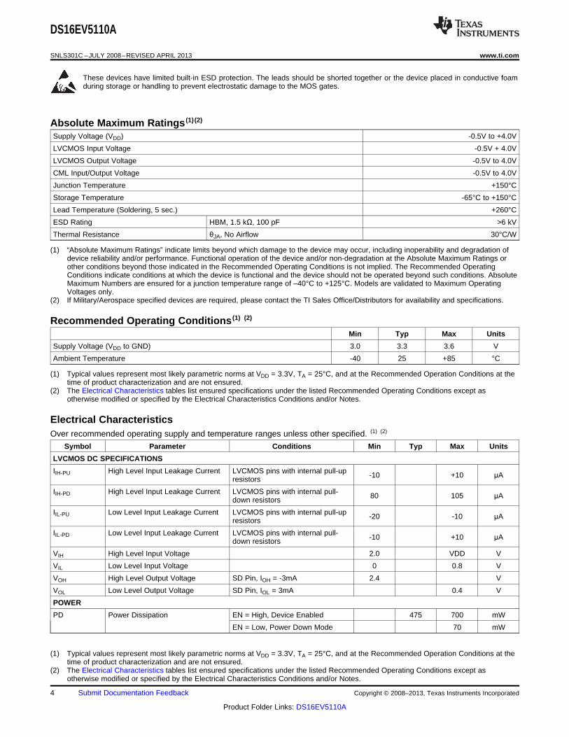
DS16EV5110A
www.ti.com SNLS301C –JULY 2008–REVISED APRIL 2013
Video Equalizer (3D+C) for DVI, HDMI Source/Repeater/Sink ApplicationsCheck for Samples: DS16EV5110A
1FEATURES DESCRIPTIONThe DS16EV5110A is a multi-channel equalizer
2• 8 Levels of Equalization Settable by 3 Pins oroptimized for video cable extensionThrough the SMBus InterfaceSource/Repeater/Sink Applications. It operates
• DC-Coupled Inputs and Outputs between 250Mbps and 2.25Gbps with common• Optimized for Operation From 250 Mbps to applications at 1.65Gbps and 2.25Gbps (per data
channel). It contains three Transition-Minimized2.25 Gbps in Support of UXGA, 480 I/P, 720 I/P,Differential Signaling (TMDS) data channels and one1080 I, and 1080 P With 8, 10, and 12-Bit Colorclock channel as specified for DVI and HDMIDepth Resolutionsinterfaces. It provides compensation for skin-effect
• Two DS16EV5110A Devices Support DVI/HDMI and dielectric losses, a common phenomenon whenDual Link transmitting video on commercially available high
• DVI 1.0, and HDMI 1.3a Compatible TMDS definition video cables.Interface The inputs conform to DVI and HDMI requirements
• Clock Channel Signal Detect (LOS) and features programmable levels of inputequalization. The programmable levels of• Enable for Power Savings Standby Modeequalization provide optimal signal boost and reduces• System Management Bus (SMBus) Providesinter-symbol interference. Eight levels of boost areControl of Boost, Output Amplitude, Enable, selectable via a pin interface or by the optional
and Clock Channel Signal Detect Threshold System Management Bus.• Low Power Consumption: 475mW (Typical)
The clock channel is optimized for clock rates of up to• 0.13 UI Total Jitter at 1.65 Gbps Including 225 MHz and features a signal detect circuit. To
Cable maximize noise immunity, the DS16EV5110Afeatures a signal detector with programmable• Single 3.3V Power Supplythresholds. The threshold is adjustable through a• Small 7mm x 7mm, 48-Pin Leadless WQFNSystem Management Bus (SMBus) interface.PackageThe DS16EV5110A may be used in Source• -40°C to +85°C Operating Temperature RangeApplications, Sink Applications, or as a Repeater.
• Extends TMDS Cable Reach Over:The DS16EV5110A also provides support for system1. > 40 Meters 24 AWG DVI Cable (1.65Gbps)power management via output enable controls.
2. > 20 Meters 28 AWG DVI Cable (1.65Gbps) Additional controls are provided via the SMBusenabling customization and optimization for specific3. > 20 Meters Cat5/Cat5e/Cat6 Cablesapplications requirements. These controls include(1.65Gbps)programmable features such as output amplitude and
4. > 20 Meters 28 AWG HDMI Cables boost controls as well as system level diagnostics.(2.25Gbps)
The DS16EV5110A is a pin-for-pin replacement tothe DS16EV5110. It features an enhanced CMLAPPLICATIONSoutput that presents a high impedance when powered
• HDMI / DVI Cable Extenders down.• HDMI / DVI Switches• Projectors• High Definition Displays
1
Please be aware that an important notice concerning availability, standard warranty, and use in critical applications ofTexas Instruments semiconductor products and disclaimers thereto appears at the end of this data sheet.
2All trademarks are the property of their respective owners.
PRODUCTION DATA information is current as of publication date. Copyright © 2008–2013, Texas Instruments IncorporatedProducts conform to specifications per the terms of the TexasInstruments standard warranty. Production processing does notnecessarily include testing of all parameters.

DES/Display Processor
DVI/HDMI Sink5m 28 AWG DVI/HDMI Cable
DS16EV5110A
DS16EV5110A DES/Display Processor
DVI/HDMI Sink25m 28 AWG DVI/HDMI Cable
SER/A/V Decoder
DVI/HDMI Source
SER A/V Decoder
DVI/HDMI Source
SER/A/V Decoder
DVI/HDMI SourceDES/Display Processor
DVI/HDMI Sink
25m 28 AWG DVI/HDMI Cable
DS16EV5110A
DVI/HDMI Repeater
1m 28 AWG DVI/HDMI Cable
DS16EV5110A
SNLS301C –JULY 2008–REVISED APRIL 2013 www.ti.com
Typical Application
PIN DESCRIPTIONSPin Name Pin Number I/O (1), Type Description
HIGH SPEED DIFFERENTIAL I/O
C_IN− 1 I, CML Inverting and non-inverting TMDS Clock inputs to the equalizer. An on-chip 50Ω terminatingC_IN+ 2 resistor connects C_IN+ to VDD and C_IN- to VDD.
D_IN0− 4 I, CML Inverting and non-inverting TMDS Data inputs to the equalizer. An on-chip 50Ω terminatingD_IN0+ 5 resistor connects D_IN0+ to VDD and D_IN0- to VDD.
D_IN1− 8 I, CML Inverting and non-inverting TMDS Data inputs to the equalizer. An on-chip 50Ω terminatingD_IN1+ 9 resistor connects D_IN1+ to VDD and D_IN1- to VDD.
D_IN2− 11 I, CML Inverting and non-inverting TMDS Data inputs to the equalizer. An on-chip 50Ω terminatingD_IN2+ 12 resistor connects D_IN2+ to VDD and D_IN2- to VDD.
C_OUT- 36 O, CML Inverting and non-inverting TMDS outputs from the equalizer. Open collector.C_OUT+ 35
D_OUT0− 33 O, CML Inverting and non-inverting TMDS outputs from the equalizer. Open collector.D_OUT0+ 32
D_OUT1– 29 O, CML Inverting and non-inverting TMDS outputs from the equalizer. Open collector.D_OUT1+ 28
D_OUT2− 26 O, CML Inverting and non-inverting TMDS outputs from the equalizer. Open collector.D_OUT2+ 25
Equalization Control
BST_0 23 I, LVCMOS BST_0, BST_1, and BST_2 select the equalizer boost level for EQ channels. BST_0, BST_1,BST_1 14 and BST_2 are internally pulled Low. See Table 2.BST_2 37
Device Control
EN 44 I, LVCMOS Enable Equalizer input. When held High, normal operation is selected. When held Low,standby mode is selected. EN is internally pulled High. Signal is global to all Data and Clockchannels.
FEB 21 I, LVCMOS Force External Boost. When held High, the equalizer boost setting is controlled by theBST_[0:2] pins. When held Low, the equalizer boost level is controlled through the SMBus(see Table 1) control pins. FEB is internally pulled High.
SD 45 O, LVCMOS Equalizer Clock Channel Signal Detect Output. Produces a High when signal is detected.
POWER
VDD 3, 6, 7, Power VDD pins should be tied to the VDD plane through a low inductance path. A 0.1µF bypass10, 13, capacitor should be connected between each VDD pin to the GND planes.15, 46
GND 22, 24, GND Ground reference. GND should be tied to a solid ground plane through a low impedance27, 30, path.31, 34
Exposed Pad DAP GND The exposed pad at the center of the package must be connected to the ground plane.
(1) Note: I = Input,O = Output, IO =Input/Output,
2 Submit Documentation Feedback Copyright © 2008–2013, Texas Instruments Incorporated
Product Folder Links: DS16EV5110A

DAP = GND
DS16EV5110ASQ(Top View)
1
2
3
4
5
6
7
8
9
10
11
12
13 14 15 16 17 18 19 20 21 22 23 24
36
35
34
33
32
31
30
29
28
27
26
25
48 47 46 45 44 43 42 41 40 39 38 37
D_IN2+
D_IN2-
D_IN1+
D_IN1-
D_IN0+
D_IN0-
C_IN+
C_IN-
D_OUT2+
D_OUT2-
D_OUT1+
D_OUT1-
D_OUT0+
D_OUT0-
C_OUT+
C_OUT-
VDD
VDD
VDD
VDD GND
GND
GND
GND
VD
D
VD
D
GN
D
GN
D
BS
T_1
BS
T_0CS
SD
C
SD
A
Res
erv
VD
D
SD
EN
Res
erv
Res
erv
Res
erv
Res
erv
Res
erv
Res
erv
Res
erv
BS
T_2
Res
erv
FE
B
Res
erv
DS16EV5110A
www.ti.com SNLS301C –JULY 2008–REVISED APRIL 2013
PIN DESCRIPTIONS (continued)
Pin Name Pin Number I/O (1), Type Description
System Management Bus (SMBus) Interface Control Pins
SDA 18 IO, LVCMOS SMBus Data Input / Output. Internally pulled High to 3.3V with High-Z pull up.
SDC 17 I, LVCMOS SMBus Clock Input. Internally pulled High to 3.3V with High-Z pull up.
CS 16 I, LVCMOS SMBus Chip select. When held High, the equalizer SMBus register is enabled. When heldLow, the equalizer SMBus register is disabled. CS is internally pulled Low. CS is internallygated with SDC.
Other
Reserv 19, 20, 38, Reserved. Do not connect.39, 40,41,42, 43, 47,
48
Connection Diagram
TOP VIEW — Not to Scale
Copyright © 2008–2013, Texas Instruments Incorporated Submit Documentation Feedback 3
Product Folder Links: DS16EV5110A
DS16EV5110A
SNLS301C –JULY 2008–REVISED APRIL 2013 www.ti.com
These devices have limited built-in ESD protection. The leads should be shorted together or the device placed in conductive foamduring storage or handling to prevent electrostatic damage to the MOS gates.
Absolute Maximum Ratings (1) (2)
Supply Voltage (VDD) -0.5V to +4.0V
LVCMOS Input Voltage -0.5V + 4.0V
LVCMOS Output Voltage -0.5V to 4.0V
CML Input/Output Voltage -0.5V to 4.0V
Junction Temperature +150°C
Storage Temperature -65°C to +150°C
Lead Temperature (Soldering, 5 sec.) +260°C
ESD Rating HBM, 1.5 kΩ, 100 pF >6 kV
Thermal Resistance θJA, No Airflow 30°C/W
(1) “Absolute Maximum Ratings” indicate limits beyond which damage to the device may occur, including inoperability and degradation ofdevice reliability and/or performance. Functional operation of the device and/or non-degradation at the Absolute Maximum Ratings orother conditions beyond those indicated in the Recommended Operating Conditions is not implied. The Recommended OperatingConditions indicate conditions at which the device is functional and the device should not be operated beyond such conditions. AbsoluteMaximum Numbers are ensured for a junction temperature range of –40°C to +125°C. Models are validated to Maximum OperatingVoltages only.
(2) If Military/Aerospace specified devices are required, please contact the TI Sales Office/Distributors for availability and specifications.
Recommended Operating Conditions (1) (2)
Min Typ Max Units
Supply Voltage (VDD to GND) 3.0 3.3 3.6 V
Ambient Temperature -40 25 +85 °C
(1) Typical values represent most likely parametric norms at VDD = 3.3V, TA = 25°C, and at the Recommended Operation Conditions at thetime of product characterization and are not ensured.
(2) The Electrical Characteristics tables list ensured specifications under the listed Recommended Operating Conditions except asotherwise modified or specified by the Electrical Characteristics Conditions and/or Notes.
Electrical CharacteristicsOver recommended operating supply and temperature ranges unless other specified. (1) (2)
Symbol Parameter Conditions Min Typ Max Units
LVCMOS DC SPECIFICATIONS
IIH-PU High Level Input Leakage Current LVCMOS pins with internal pull-up -10 +10 μAresistors
IIH-PD High Level Input Leakage Current LVCMOS pins with internal pull- 80 105 μAdown resistors
IIL-PU Low Level Input Leakage Current LVCMOS pins with internal pull-up -20 -10 μAresistors
IIL-PD Low Level Input Leakage Current LVCMOS pins with internal pull- -10 +10 μAdown resistors
VIH High Level Input Voltage 2.0 VDD V
VIL Low Level Input Voltage 0 0.8 V
VOH High Level Output Voltage SD Pin, IOH = -3mA 2.4 V
VOL Low Level Output Voltage SD Pin, IOL = 3mA 0.4 V
POWER
PD Power Dissipation EN = High, Device Enabled 475 700 mW
EN = Low, Power Down Mode 70 mW
(1) Typical values represent most likely parametric norms at VDD = 3.3V, TA = 25°C, and at the Recommended Operation Conditions at thetime of product characterization and are not ensured.
(2) The Electrical Characteristics tables list ensured specifications under the listed Recommended Operating Conditions except asotherwise modified or specified by the Electrical Characteristics Conditions and/or Notes.
4 Submit Documentation Feedback Copyright © 2008–2013, Texas Instruments Incorporated
Product Folder Links: DS16EV5110A

DS16EV5110A
www.ti.com SNLS301C –JULY 2008–REVISED APRIL 2013
Electrical Characteristics (continued)Over recommended operating supply and temperature ranges unless other specified. (1) (2)
Symbol Parameter Conditions Min Typ Max Units
N Supply Noise Tolerance (3) DC to 50MHz 100 mVP-P
CML INPUTS
VTX Input Voltage Swing (Launch Measured differentially at TPA 800 1200 mVP-PAmplitude) (Figure 2)
VICMDC Input Common-Mode Voltage DC-Coupled Requirement VDD-0.3 VDD-0.2 VMeasured at TPA (Figure 2)
VIN Input Voltage Swing Measured differentially at TPB 120 mVP-P(Figure 2)
RLI Differential Input Return Loss 100 MHz– 825 MHz, with fixture's 10 dBeffect de-embedded
RIN Input Resistance IN+ to VDD and IN− to VDD 45 50 55 ΩCML OUTPUTS
VO Output Voltage Swing Measured differentially with OUT+and OUT− terminated by 50Ω to 800 1200 mVP-PVDD
VOCM Output common-mode Voltage Measured Single-ended VDD-0.3 VDD-0.2 V
IOFF Output Leakage Current VOUT = 3.6V, VDD = open or 0V ±1 µA
tR, tF Transition Time 20% to 80% of differential outputvoltage, measured within 1" from 75 240 psoutput pins.
tCCSK Inter Pair Channel-to-Channel Difference in 50% crossingSkew (all 4 Channels) between shortest and longest 25 ps
channels
tD Latency 350 ps
OUTPUT JITTER
TJ1 Total Jitter at 1.65 Gbps 20m 28 AWG STP DVI CableData Paths 0.13 0.17 UIP-PEQ Setting 0x04 PRBS7 (4) (5) (6)
TJ2 Total Jitter at 2.25 Gbps 20m 28 AWG STP DVI CableData Paths 0.2 UIP-PEQ Setting 0x04 PRBS7 (4) (5) (6)
TJ3 Total Jitter at 165 MHz Clock Paths 0.165 UIP-PClock Pattern (4) (5) (6)
TJ4 Total Jitter at 225 MHz Clock Paths 0.165 UIP-PClock Pattern (4) (5) (6)
RJ Random Jitter See (6) (7) 3 psrms
BIT RATE
FCLK Clock Frequency Clock Path (4) 25 225 MHz
BR Bit Rate Data Path (4) 0.25 2.25 Gbps
(3) Allowed supply noise (mVP-P sine wave) under typical conditions.(4) Specification is ensured by characterization and is not tested in production.(5) Deterministic jitter is measured at the differential outputs (TPC of Figure 2), minus the deterministic jitter before the test channel (TPA of
Figure 2). Random jitter is removed through the use of averaging or similar means.(6) Total Jitter is defined as peak-to-peak deterministic jitter from () + 14.2 times random jitter in psrms.(7) Random jitter contributed by the equalizer is defined as sq rt (JOUT
2 − JIN2). JOUT is the random jitter at equalizer outputs in psrms, see
TPC of Figure 2; JIN is the random jitter at the input of the equalizer in psrms, see TPA of Figure 2.
Copyright © 2008–2013, Texas Instruments Incorporated Submit Documentation Feedback 5
Product Folder Links: DS16EV5110A

DS16EV5110A
SNLS301C –JULY 2008–REVISED APRIL 2013 www.ti.com
Electrical Characteristics — System Management Bus Interface (1) (2)
Over recommended operating supply and temperature ranges unless other specified.
Symbol Parameter Conditions Min Typ Max Units
System Bus Interface — DC Specifications
VIL Data, Clock Input Low Voltage 0.8 V
VIH Data, Clock Input High Voltage 2.8 VDD V
IPULLUP Current through pull-up resistor or VOL = 0.4V 10 mAcurrent source
VDD Nominal Bus Voltage 3.0 3.6 V
ILEAK-Bus Input Leakage per bus segment (3) -200 +200 µA
ILEAK-Pin Input Leakage per device pin -15 µA
CI Capacitance for SDA and SDC (3) (4) 10 pF
RTERM Termination Resistance VDD3.3, (3) (4) (5) 1000 ΩSystem Bus Interface Timing Specification
FSMB Bus Operating Frequency (6) 10 100 kHz
TBUF Bus Free Time Between Stop and 4.7 µsStart Condition
TSU:CS Minimum time between SMB_CS (7)30 nsbeing active and start condition
TH:CS Minimum time between stop (7)100 nscondition and releasing SMB_CS
THD:STA Hold Time After (Repeated) Start At IPULLUP, MaxCondition. First CLK generated 4.0 µsafter this period.
TSU:STA Repeated Start Condition Setup 4.7 µsTime
TSU:STO Stop Condition Setup Time 4.0 µs
THD:DAT Data Hold Time 300 ns
TSU:DAT Data Setup Time 250 ns
TTIMEOUT Detect Clock Low Timeout (6) 25 35 ms
TLOW Clock Low Period 4.7 µs
THIGH Clock High Period (6) 4.0 50 µs
TLOW:SEXT Cumulative Clock Low Extend Time (6)2 ms(Slave Device)
tF Clock/Data Fall Time (6) 300 ns
tR Clock/Data Rise Time (6) 1000 ns
tPOR Time in which a device must be (6)500 msoperational after power-on reset
(1) Typical values represent most likely parametric norms at VDD = 3.3V, TA = 25°C, and at the Recommended Operation Conditions at thetime of product characterization and are not ensured.
(2) The Electrical Characteristics tables list ensured specifications under the listed Recommended Operating Conditions except asotherwise modified or specified by the Electrical Characteristics Conditions and/or Notes.
(3) Recommended value. Parameter not tested in production.(4) Recommended maximum capacitance load per bus segment is 400pF.(5) Maximum termination voltage should be identical to the device supply voltage.(6) Compliant to SMBus 2.0 physical layer specification. See System Management Bus (SMBus) Specification Version 2.0, section 3.1.1
SMBus common AC specifications for details.(7) Specification is ensured by characterization and is not tested in production.
6 Submit Documentation Feedback Copyright © 2008–2013, Texas Instruments Incorporated
Product Folder Links: DS16EV5110A
Pat
tern
G
ener
ator
100
mV
PP
Diff
eren
tial
SM
A to
HD
MI
Ada
pter
DS
16E
V51
10A
SM
A to
HD
MI
Ada
pter
Jitte
r T
est
Inst
rum
ent
CoaxSMA
CoaxSMA
CoaxSMA
CoaxSMA
CoaxSMA
CoaxSMA
CoaxSMA
VDD
RLoadRLoad
VDD
RLoadRLoad
VDD
RLoadRLoad
RLoadRLoad
CoaxSMA
VDD
RLoadRLoad
VDD
RLoadRLoad
VDD
RLoadRLoad
VDD
RLoadRLoad
28 AWGDVI/HDMI
Cable
VDD
TPCTPBTPA
SMA
SMA
SMA
SMA
SMA
SMA
SMA
SMA
Coax
Coax
Coax
Coax
Coax
Coax
Coax
Coax
Clk-
Clk+
Data0-
Data0+
Data1-
Data1+
Data2-
Data2+
TPD
SP
tBUFtHD:STA
tLOW
tR
tHD:DAT
tHIGH
tFtSU:DAT
tSU:STA
ST SP
tSU:STO
SCK
SDA
SMB_CStSU:CS
ST
tH:CS
DS16EV5110A
www.ti.com SNLS301C –JULY 2008–REVISED APRIL 2013
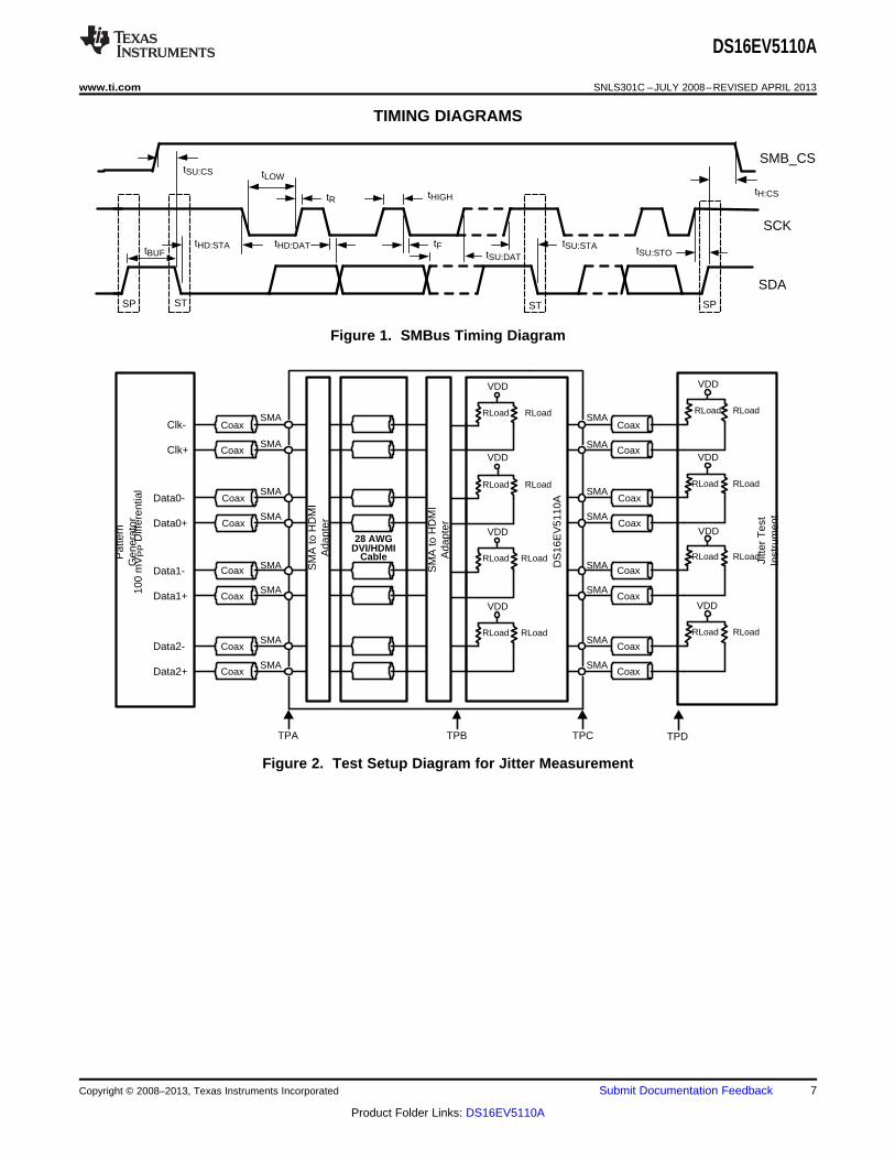
TIMING DIAGRAMS
Figure 1. SMBus Timing Diagram
Figure 2. Test Setup Diagram for Jitter Measurement
Copyright © 2008–2013, Texas Instruments Incorporated Submit Documentation Feedback 7
Product Folder Links: DS16EV5110A

DS16EV5110A
SNLS301C –JULY 2008–REVISED APRIL 2013 www.ti.com
SYSTEM MANAGEMENT BUS (SMBUS) AND CONFIGURATION REGISTERS
The System Management Bus interface is compatible to SMBus 2.0 physical layer specification. The use of theChip Select signal is required. Holding the CS pin High enables the SMBus port allowing access to theconfiguration registers. Holding the CS pin Low disables the device's SMBus allowing communication from thehost to other slave devices on the bus. In the STANDBY state, the System Management Bus remains active.When communication to other devices on the SMBus is active, the CS signal for the DS16EV5110As must bedriven Low.
The address byte for all DS16EV5110As is AC'h. Based on the SMBus 2.0 specification, the DS16EV5110A hasa 7-bit slave address of 1010110'b. The LSB is set to 0'b (for a WRITE), thus the 8-bit value is 1010 1100 'b orAC'h.
The SDC and SDA pins are 3.3V LVCMOS signaling and include high-Z internal pull up resistors. External lowimpedance pull up resistors maybe required depending upon SMBus loading and speed. Note, these pins are not5V tolerant.
Transfer of Data via the SMBus
During normal operation the data on SDA must be stable during the time when SDC is High.
There are three unique states for the SMBus:
START: A High-to-Low transition on SDA while SDC is High indicates a message START condition.
STOP: A Low-to-High transition on SDA while SDC is High indicates a message STOP condition.
IDLE: If SDC and SDA are both High for a time exceeding tBUF from the last detected STOP condition or if theyare High for a total exceeding the maximum specification for tHIGH then the bus will transfer to the IDLE state.
SMBus Transactions
The device supports WRITE and READ transactions. See Table 1 for register address, type (Read/Write, ReadOnly), default value and function information.
Writing a Register
To write a register, the following protocol is used (see SMBus 2.0 specification).1. The Host (Master) selects the device by driving its SMBus Chip Select (CS) signal High.2. The Host drives a START condition, the 7-bit SMBus address, and a “0” indicating a WRITE.3. The Device (Slave) drives the ACK bit (“0”).4. The Host drives the 8-bit Register Address.5. The Device drives an ACK bit (“0”).6. The Host drive the 8-bit data byte.7. The Device drives an ACK bit (“0”).8. The Host drives a STOP condition.9. The Host de-selects the device by driving its SMBus CS signal Low.
The WRITE transaction is completed, the bus goes IDLE and communication with other SMBus devices maynow occur.
Reading a Register
To read a register, the following protocol is used (see SMBus 2.0 specification).1. The Host (Master) selects the device by driving its SMBus Chip Select (CS) signal High.2. The Host drives a START condition, the 7-bit SMBus address, and a “0” indicating a WRITE.3. The Device (Slave) drives the ACK bit (“0”).4. The Host drives the 8-bit Register Address.5. The Device drives an ACK bit (“0”).6. The Host drives a START condition.7. The Host drives the 7-bit SMBus Address, and a “1” indicating a READ.8. The Device drives an ACK bit “0”.
8 Submit Documentation Feedback Copyright © 2008–2013, Texas Instruments Incorporated
Product Folder Links: DS16EV5110A

DS16EV5110A
www.ti.com SNLS301C –JULY 2008–REVISED APRIL 2013
9. The Device drives the 8-bit data value (register contents).10. The Host drives a NACK bit “1”indicating end of the READ transfer.11. The Host drives a STOP condition.12. The Host de-selects the device by driving its SMBus CS signal Low.
The READ transaction is completed, the bus goes IDLE and communication with other SMBus devices may nowoccur.
Please see Table 1 for more information.
Table 1. SMBus Register Descriptions
Name Address Default Type (1) Bit 7 Bit 6 Bit 5 Bit 4 Bit 3 Bit 2 Bit 1 Bit 0
Status 0x00 0x00 RO ID Revision Reserved Reserved Reserve SDd
Status 0x01 0x00 RO Reserved Boost 1 EN Reserved
Status 0x02 0x00 RO Reserved Boost 3 Reserved Boost 2
Internal 0x03 0x77 RW EN (Int.) Boost Control EN (Int.) ReservedEnable/ 0:Enable (BC for CH0) 0:EnableIndividual 1:Disable 000 (Min Boost) 1:DisableChannel (D_IN0±) 001 (C_IN±)Boost 010Control 011for 100C_IN±, 101D_IN0± 110
111 (Max Boost)
Individual 0x04 0x77 RW EN (Int.) Boost Control EN (Int.) Boost ControlChannel 0:Enable (BC for CH2) 0:Enable (BC for CH1)Boost 1:Disable 000 (Min Boost) 1:Disable 000 (Min Boost)Control (D_IN2±) 001 (D_IN1±) 001for 010 010D_IN1±, 011 011D_IN2± 100 100
101 101110 110111 (Max Boost) 111 (Max Boost)
Signal 0x05 0x00 RW Reserved Threshold (mV)Detect ON 00: 70 (Default)(SD_ON) 01: 55
10: 9011: 75
Signal 0x06 0x00 RW Reserved Threshold (mV)Detect OFF 00: 40 (Default)(SD_OFF) 01: 30
10: 5511: 45
SMBus 0x07 0x00 RW Reserved SMBusorCMOS EnableControl for 0: DisableEN 1: Enable
Output 0x08 0x78 RW Reserved Output Level: ReservedLevel 00: 540 mVp-p
01: 770 mVp-p10: 1000 mVp-p11: 1200 mVp-p
(1) Note: RO = Read Only, RW = Read/Write
Copyright © 2008–2013, Texas Instruments Incorporated Submit Documentation Feedback 9
Product Folder Links: DS16EV5110A

DS16EV5110A
SNLS301C –JULY 2008–REVISED APRIL 2013 www.ti.com
DS16EV5110A DEVICE DESCRIPTION
The DS16EV5110A video equalizer comprises three data channels, a clock channel, and a control interfaceincluding a Systeml Management Bus (SMBus) port.
DATA CHANNELS
The DS16EV5110A provides three data channels. Each data channel consists of an equalizer stage, a limitingamplifier, a DC offset correction block, and a TMDS driver as shown in Figure 3.
EQUALIZER BOOST CONTROL
The data channel equalizers support eight programmable levels of equalization boost. The state of the FEB pindetermines how the boost settings are controlled. If the FEB pin is held High, then the equalizer boost setting iscontrolled by the Boost Set pins (BST_[0:2]) in accordance with Table 2. If this programming method is chosen,then the boost setting selected on the Boost Set pins is applied to all three data channels. When the FEB pin isheld Low, the equalizer boost level is controlled through the SMBus. This programming method is accessed viathe appropriate SMBus registers (see Table 1). Using this approach, equalizer boost settings can beprogrammed for each channel individually. FEB is internally pulled High (default setting); therefore if leftunconnected, the boost settings are controlled by the Boost Set pins (BST_[0:2]). The range of boost settingsprovided enables the DS16EV5110A to address a wide range of transmission line path loss scenarios, enablingsupport for a variety of data rates and formats.
Table 2. EQ Boost Control Table
Control Via SMBus Control Via Pins EQ Boost Setting atBC_2, BC_1, BC_0 BST_2, BST_1, 825 MHz (dB)
(FEB = 0) BST_0 (TYP)(FEB = 1)
000 000 9
001 001 14
010 010 18
011 011 21
100 100 24
101 101 26
110 110 28
111 111 30
DEVICE STATE AND ENABLE CONTROL
The DS16EV5110A has an Enable feature which provides the ability to control device power consumption. Thisfeature can be controlled either via the Enable Pin (EN Pin) or via the Enable Control Bit which is accessedthrough the SMBus port (see Table 1 and Table 3). If Enable is activated, the data channels and clock channelare placed in the ACTIVE state and all device blocks function as described. The DS16EV5110A can also beplaced in STANDBY mode to save power. In this mode only the control interface including the SMBus port aswell as the clock channel signal detection circuit remain active.
Table 3. Enable and Device State Control
Register 07[0] EN Pin Register 03[3] (EN Device State(SMBus) (CMOS) Control)
(SMBus)
0 : Disable 1 X ACTIVE
0 : Disable 0 X STANDBY
1 : Enable X 0 ACTIVE
1 : Enable X 1 STANDBY
10 Submit Documentation Feedback Copyright © 2008–2013, Texas Instruments Incorporated
Product Folder Links: DS16EV5110A

InputTermination
Equalizer LimitingAmplifier
DC Offset CorrectionData Channel (0-2)
Boost Setting
3
33
BST_0 : BST_2
BST CNTL EN EN EN
FEB
SMBus Reg.REG3[7], REG4[7], REG4[3]
EN
SMBus Register
D_OUT+D_OUT-
D_IN+D_IN-
SMBus Reg.REG7[0]
DS16EV5110A
www.ti.com SNLS301C –JULY 2008–REVISED APRIL 2013
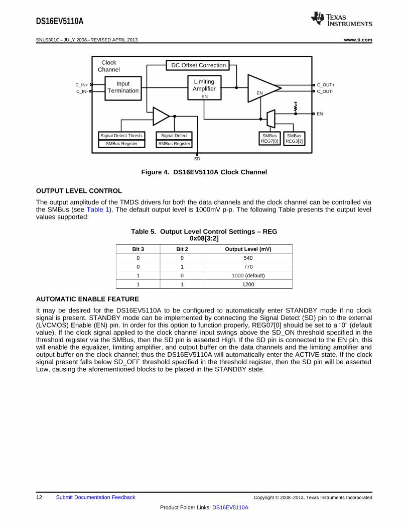
CLOCK CHANNEL
The clock channel incorporates a limiting amplifier, a DC offset correction, and a TMDS driver as shown inFigure 4.
CLOCK CHANNEL SIGNAL DETECT
The DS16EV5110A features a signal detect circuit on the clock channel. The status of the clock signal can bedetermined by either reading the Signal Detect bit (SD) in the SMBus registers (see Table 1) or by the state ofthe SD pin. A logic High indicates the presence of a signal that has exceeded a specified threshold value (calledSD_ON). A logic Low means that the clock signal has fallen below a threshold value (called SD_OFF). Thesevalues are programmed via the SMBus (Table 1). If not programmed via the SMBus, the thresholds take on thedefault values for the SD_OFF and SD_ON values as indicated in Table 4. The Signal Detect threshold valuescan be changed through the SMBus. All threshold values specified are DC peak-to-peak differential signals(positive signal minus negative signal) at the input of the device.
Table 4. Clock Channel Signal Detect ThresholdValues
Bit 1 Bit 0 SD_OFF Threshold SD_ON ThresholdRegister 06 (mV) Register 05 (mV)
0 0 40 (Default) 70 (Default)
0 1 30 55
1 0 55 90
1 1 45 75
Figure 3. DS16EV5110A Data Channel
Copyright © 2008–2013, Texas Instruments Incorporated Submit Documentation Feedback 11
Product Folder Links: DS16EV5110A
InputTermination
LimitingAmplifier
DC Offset CorrectionClock Channel
EN
SMBus REG3[3]
EN
EN
Signal Detect Thresh.
SMBus Register
Signal Detect
SMBus Register
SD
C_OUT-
C_OUT+
C_IN-
C_IN+
SMBus REG7[0]
DS16EV5110A
SNLS301C –JULY 2008–REVISED APRIL 2013 www.ti.com
Figure 4. DS16EV5110A Clock Channel
OUTPUT LEVEL CONTROL
The output amplitude of the TMDS drivers for both the data channels and the clock channel can be controlled viathe SMBus (see Table 1). The default output level is 1000mV p-p. The following Table presents the output levelvalues supported:
Table 5. Output Level Control Settings – REG0x08[3:2]
Bit 3 Bit 2 Output Level (mV)
0 0 540
0 1 770
1 0 1000 (default)
1 1 1200
AUTOMATIC ENABLE FEATURE
It may be desired for the DS16EV5110A to be configured to automatically enter STANDBY mode if no clocksignal is present. STANDBY mode can be implemented by connecting the Signal Detect (SD) pin to the external(LVCMOS) Enable (EN) pin. In order for this option to function properly, REG07[0] should be set to a “0” (defaultvalue). If the clock signal applied to the clock channel input swings above the SD_ON threshold specified in thethreshold register via the SMBus, then the SD pin is asserted High. If the SD pin is connected to the EN pin, thiswill enable the equalizer, limiting amplifier, and output buffer on the data channels and the limiting amplifier andoutput buffer on the clock channel; thus the DS16EV5110A will automatically enter the ACTIVE state. If the clocksignal present falls below SD_OFF threshold specified in the threshold register, then the SD pin will be assertedLow, causing the aforementioned blocks to be placed in the STANDBY state.
12 Submit Documentation Feedback Copyright © 2008–2013, Texas Instruments Incorporated
Product Folder Links: DS16EV5110A

DS16EV5110DS16EV5110
20m DVI/HDMI Cable
HDTV
DVI/HDMI DVD
Player
DVI/HDMI Extender
To HDTV 20m DVI/HDMI Cable
Data 2 OUT +/-
Data 1 OUT +/-
Data 0 OUT +/-
Clock OUT +/-
Data 1 IN +/-
Data 0 IN +/-
Clock IN +/-
Data 2 IN +/-
DVI/HDMI Extender
DS16EV5110A
DVI/HDMI Source(e.g. DVD Player)
DS16EV5110ADES/Display
Controller
DVI/HDMI Sink(e.g. HDTV)
20m 28 AWG DVI/HDMI Cable
DES/Display Processor
DVI/HDMI Sink
5m 28 AWG DVI/HDMI Cable
DS16EV5110ASER/A/V Decoder
DVI/HDMI Source
DS16EV5110A
www.ti.com SNLS301C –JULY 2008–REVISED APRIL 2013
APPLICATION INFORMATION
The DS16EV5110A is used to recondition DVI/HDMI video signals or differential signals with similarcharacteristics for signal loss and degradation due to transmission through a length of shielded or unshieldedcable. The DS16EV5110A maybe used on the Source or Sink side of the application or as a Repeater (Sink andSource).
In the Source Side application the DS16EV5110A is located near the Serializer and conditions the signal forlosses due to internal cabling or FR4 losses (backplane). The signal is then re-driven at full amplitude andreduced jitter over the external cable interconnect.
Figure 5. DS16EV5110A Source-Side Application
In the Sink Side application the DS16EV5110A is located next to the Deserializer and post-conditions the signalfor losses incurred over the cable interconnect.
Figure 6. DS16EV5110A Sink-Side Application
The DS16EV5110A may be used in repeater type application as shown in Figure 7 . The cable on the output ofthe repeater tends to be shorter and may be a dongle type application. The input of the repeater recovers thesignal after transmission over a long cable interconnect.
Figure 7. DS16EV5110A Repeater Application with CAT 5 Cable
In general, the use of multiple equalizers is not recommended due to accumulation of random jitter.
Copyright © 2008–2013, Texas Instruments Incorporated Submit Documentation Feedback 13
Product Folder Links: DS16EV5110A

DS16EV5110A
DS16EV5110A
D0
D1
D2
CLK
D3
D4
D5
D0
D1
D2
CLK
D3
D4
D5
CLK CLK
SD
SD
EN
EN CS
CS
DS16EV5110A
SNLS301C –JULY 2008–REVISED APRIL 2013 www.ti.com
DVI 1.0 AND HDMI V1.2a APPLICATIONS
A single DS16EV5110A can be used to implement cable extension solutions with various resolutions and screenrefresh rates. The range of digital serial rates supported is between 250 Mbps and 1.65 Gbps. For applicationsrequiring ultra-high resolution for DVI applications (e.g., QXGA and WQXGA), a “dual link” TMDS interface isrequired. This is easily configured by using two DS16EV5110A devices as shown in Figure 8.
Note the recommended connections between LVCMOS control pins. This provides the Automatic Enable featurefor both devices based on the one active clock channel. In many applications the SMBus is not required (deviceis pin controlled), for this application simply leave the three SMBus pins open. SDC and SDA are internally pulledHigh, and CS is internally pulled Low, thus the SMBus is in the disabled state.
Figure 8. Connection in Dual Link Application
HDMI V1.3 APPLICATION
The DS16EV5110A can reliably extend operation to distances greater than 20 meters of 28 AWG HDMI cable at2.25 Gbps, thereby supporting HDMI v1.3 for 1080p HDTV resolution with 12-bit color depth. Please note thatthe Electrical Characteristics specified in this document have not been tested for and are not ensured for 2.25Gbps operation.
DC COUPLED DATA PATHS AND DVI/HDMI COMPLIANCE
The DS16EV5110A is designed to support TMDS differential pairs with DC coupled transmission lines. Itcontains integrated termination resistors (50Ω), pulled up to VDD at the input stage, and open collector outputsfor DVI / HDMI for signal swing.
CABLE SELECTION
At higher frequencies, longer cable lengths produce greater losses due to the skin effect. The quality of the cablewith respect to conductor wire gauge and shielding heavily influences performance. Thicker conductors havelower signal degradation per unit length. In nearly all applications, the DS16EV5110A equalization can be set to0x04, and equalize up to 22 dB skin effect loss for all input cable configurations at all data rates, withoutdegrading signal integrity.
28 AWG STP DVI / HDMI CABLES RECOMMENDED BOOST SETTINGS
The following table presents the recommended boost control settings for various data rates and cable lengths for28 AWG DVI/HDMI compliant configurations. Boost setting maybe done via the three BST[2:0] pins or via therespective register values.
14 Submit Documentation Feedback Copyright © 2008–2013, Texas Instruments Incorporated
Product Folder Links: DS16EV5110A

5 10 15 20 25 30 35
28 AWG DVI/HDMI CABLE LENGTH (m)
0
0.1
0.2
0.3
0.4
0.5T
OT
AL
JIT
TE
R (
UI)
0
2.25 Gbps
1.65 Gbps
0.75 Gbps
0.25 Gbps
Unequalized
Equalized
DS16EV5110A
www.ti.com SNLS301C –JULY 2008–REVISED APRIL 2013
Table 6. Boost Control Setting for STP Cables
Setting Data Rate 28 AWG DVI / HDMI
0x04 750 Mbps 0–25m
0x04 1.65 Gbps 0–20m
0x06 750 Mbps 25m to greater than 30m
0x06 1.65 Gbps 20m to greater than 25m
0x03 2.25 Gbps 0–15m
0x06 2.25 Gbps 15m to greater than 20m
Figure 9 shows the cable extension and jitter reduction obtained with the use of the equalizer. Table 6 lists thevarious gain settings used versus cable length recommendations.
Figure 9. Equalized vs. Unequalized Jitter Performance Over 28 AWG DVI/HDMI Cable
UTP (UNSHIELDED TWIST PAIRS) CABLES
The DS16EV5110A can be used to extend the length of UTP cables, such as Cat5, Cat5e and Cat6 to distancesgreater than 20 meters at 1.65 Gbps with < 0.13 UI of jitter. Please note that for non-standard DVI/HDMI cables,the user must ensure the clock-to-data channel skew requirements are met. Table 7 presents the recommendedboost control settings for various data rates and cable lengths for UTP configurations:
Table 7. Boost Control Setting for UTP Cables
Setting Data Rate Cat5 Cable
0x03 750 Mbps 0–25m
0x06 750 Mbps 25–45m
0x03 1.65 Gbps Greater than 20m
Copyright © 2008–2013, Texas Instruments Incorporated Submit Documentation Feedback 15
Product Folder Links: DS16EV5110A

0 5 10 15 20 25 30 35 40
CAT 5 CABLE LENGTH (m)
TO
TA
L JI
TT
ER
(U
I)
0
0.1
0.2
0.3
0.4
0.5
1.30 Gbps
0.75 Gbps
1.65 Gbps
Unequalized
Equalized
DS16EV5110A
SNLS301C –JULY 2008–REVISED APRIL 2013 www.ti.com
Figure 10 shows the cable extension and jitter reduction obtained with the use of the equalizer. Table 7 lists thevarious gain settings used versus cable length recommendations.
Figure 10. Equalized vs. Unequalized Jitter Performance Over Cat5 Cable
General Recommendations
The DS16EV5110A is a high performance circuit capable of delivering excellent performance. Careful attentionmust be paid to the details associated with high-speed design as well as providing a clean power supply. Referto the LVDS Owner’s Manual for more detailed information on high-speed design tips as well as many otheravailable resources available addressing signal integrity design issues.
PCB LAYOUT CONSIDERATIONS FOR DIFFERENTIAL PAIRS
The TMDS differential inputs and outputs must have a controlled differential impedance of 100Ω. It is preferableto route TMDS lines exclusively on one layer of the board, particularly for the input traces. The use of vias shouldbe avoided if possible. If vias must be used, they should be used sparingly and must be placed symmetrically foreach side of a given differential pair. Route the TMDS signals away from other signals and noise sources on theprinted circuit board. All traces of TMDS differential inputs and outputs must be equal in length to minimize intra-pair skew.
WQFN FOOTPRINT RECOMMENDATIONS
See application note AN-1187 (SNOA401) for additional information on WQFN packages footprint and solderinginformation.
POWER SUPPLY BYPASSING
Two approaches are recommended to ensure that the DS16EV5110A is provided with an adequate powersupply. First, the supply (VDD) and ground (GND) pins should be connected to power planes routed on adjacentlayers of the printed circuit board. The layer thickness of the dielectric should be minimized so that the VDD andGND planes create a low inductance supply with distributed capacitance. Second, careful attention to supplybypassing through the proper use of bypass capacitors is required. A 0.1µF bypass capacitor should beconnected to each VDD pin such that the capacitor is placed as close as possible to the DS16EV5110A. Smallerbody size capacitors can help facilitate proper component placement. Additionally, three capacitors withcapacitance in the range of 2.2µF to 10µF should be incorporated in the power supply bypassing design as well.These capacitors can be either tantalum or an ultra-low ESR ceramic and should be placed as close as possibleto the DS16EV5110A.
EQUIVALENT I/O STRUCTURES
Figure 11 shows the DS16EV5110A CML output structure and ESD protection circuitry.
Figure 12 shows the DS16EV5110A CML input structure and ESD protection circuitry.
16 Submit Documentation Feedback Copyright © 2008–2013, Texas Instruments Incorporated
Product Folder Links: DS16EV5110A

50:
IN+
VDD
50:
IN-
OUT+
OUT-
DS16EV5110A
www.ti.com SNLS301C –JULY 2008–REVISED APRIL 2013
Figure 11. Equivalent CML Output Structure
Figure 12. Equivalent CML Input Structure
Copyright © 2008–2013, Texas Instruments Incorporated Submit Documentation Feedback 17
Product Folder Links: DS16EV5110A
DS16EV5110A
SNLS301C –JULY 2008–REVISED APRIL 2013 www.ti.com
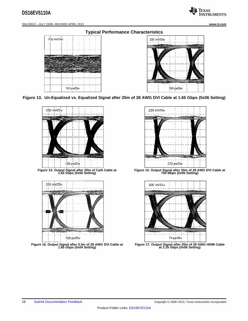
Typical Performance Characteristics
Figure 13. Un-Equalized vs. Equalized Signal after 25m of 28 AWG DVI Cable at 1.65 Gbps (0x06 Setting)
Figure 14. Output Signal after 20m of Cat5 Cable at Figure 15. Output Signal after 30m of 28 AWG DVI Cable at1.65 Gbps (0x06 Setting) 750 Mbps (0x06 Setting)
Figure 16. Output Signal after 0.3m of 28 AWG DVI Cable at Figure 17. Output Signal after 20m of 28 AWG HDMI Cable1.65 Gbps (0x04 Setting) at 2.25 Gbps (0x06 Setting)
18 Submit Documentation Feedback Copyright © 2008–2013, Texas Instruments Incorporated
Product Folder Links: DS16EV5110A
DS16EV5110A
www.ti.com SNLS301C –JULY 2008–REVISED APRIL 2013
REVISION HISTORY
Changes from Revision B (April 2013) to Revision C Page
• Changed layout of National Data Sheet to TI format .......................................................................................................... 18
Copyright © 2008–2013, Texas Instruments Incorporated Submit Documentation Feedback 19
Product Folder Links: DS16EV5110A

PACKAGE OPTION ADDENDUM
www.ti.com 13-Sep-2014
Addendum-Page 1
PACKAGING INFORMATION
Orderable Device Status(1)
Package Type PackageDrawing
Pins PackageQty
Eco Plan(2)
Lead/Ball Finish(6)
MSL Peak Temp(3)
Op Temp (°C) Device Marking(4/5)
Samples
DS16EV5110ASQ/NOPB ACTIVE WQFN NJU 48 1000 Green (RoHS& no Sb/Br)
CU SN Level-3-260C-168 HR -40 to 85 D16EV511A
DS16EV5110ASQE/NOPB ACTIVE WQFN NJU 48 250 Green (RoHS& no Sb/Br)
CU SN Level-3-260C-168 HR -40 to 85 D16EV511A
DS16EV5110ASQX/NOPB ACTIVE WQFN NJU 48 2500 Green (RoHS& no Sb/Br)
CU SN Level-3-260C-168 HR -40 to 85 D16EV511A
(1) The marketing status values are defined as follows:ACTIVE: Product device recommended for new designs.LIFEBUY: TI has announced that the device will be discontinued, and a lifetime-buy period is in effect.NRND: Not recommended for new designs. Device is in production to support existing customers, but TI does not recommend using this part in a new design.PREVIEW: Device has been announced but is not in production. Samples may or may not be available.OBSOLETE: TI has discontinued the production of the device.
(2) Eco Plan - The planned eco-friendly classification: Pb-Free (RoHS), Pb-Free (RoHS Exempt), or Green (RoHS & no Sb/Br) - please check http://www.ti.com/productcontent for the latest availabilityinformation and additional product content details.TBD: The Pb-Free/Green conversion plan has not been defined.Pb-Free (RoHS): TI's terms "Lead-Free" or "Pb-Free" mean semiconductor products that are compatible with the current RoHS requirements for all 6 substances, including the requirement thatlead not exceed 0.1% by weight in homogeneous materials. Where designed to be soldered at high temperatures, TI Pb-Free products are suitable for use in specified lead-free processes.Pb-Free (RoHS Exempt): This component has a RoHS exemption for either 1) lead-based flip-chip solder bumps used between the die and package, or 2) lead-based die adhesive used betweenthe die and leadframe. The component is otherwise considered Pb-Free (RoHS compatible) as defined above.Green (RoHS & no Sb/Br): TI defines "Green" to mean Pb-Free (RoHS compatible), and free of Bromine (Br) and Antimony (Sb) based flame retardants (Br or Sb do not exceed 0.1% by weightin homogeneous material)
(3) MSL, Peak Temp. - The Moisture Sensitivity Level rating according to the JEDEC industry standard classifications, and peak solder temperature.
(4) There may be additional marking, which relates to the logo, the lot trace code information, or the environmental category on the device.
(5) Multiple Device Markings will be inside parentheses. Only one Device Marking contained in parentheses and separated by a "~" will appear on a device. If a line is indented then it is a continuationof the previous line and the two combined represent the entire Device Marking for that device.
(6) Lead/Ball Finish - Orderable Devices may have multiple material finish options. Finish options are separated by a vertical ruled line. Lead/Ball Finish values may wrap to two lines if the finishvalue exceeds the maximum column width.
Important Information and Disclaimer:The information provided on this page represents TI's knowledge and belief as of the date that it is provided. TI bases its knowledge and belief on informationprovided by third parties, and makes no representation or warranty as to the accuracy of such information. Efforts are underway to better integrate information from third parties. TI has taken and
PACKAGE OPTION ADDENDUM
www.ti.com 13-Sep-2014
Addendum-Page 2
continues to take reasonable steps to provide representative and accurate information but may not have conducted destructive testing or chemical analysis on incoming materials and chemicals.TI and TI suppliers consider certain information to be proprietary, and thus CAS numbers and other limited information may not be available for release.
In no event shall TI's liability arising out of such information exceed the total purchase price of the TI part(s) at issue in this document sold by TI to Customer on an annual basis.
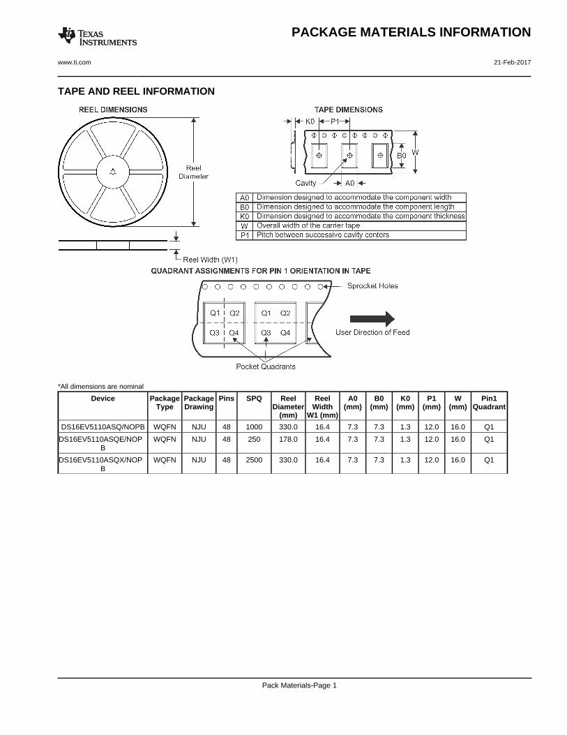
TAPE AND REEL INFORMATION
*All dimensions are nominal
Device PackageType
PackageDrawing
Pins SPQ ReelDiameter
(mm)
ReelWidth
W1 (mm)
A0(mm)
B0(mm)
K0(mm)
P1(mm)
W(mm)
Pin1Quadrant
DS16EV5110ASQ/NOPB WQFN NJU 48 1000 330.0 16.4 7.3 7.3 1.3 12.0 16.0 Q1
DS16EV5110ASQE/NOPB
WQFN NJU 48 250 178.0 16.4 7.3 7.3 1.3 12.0 16.0 Q1
DS16EV5110ASQX/NOPB
WQFN NJU 48 2500 330.0 16.4 7.3 7.3 1.3 12.0 16.0 Q1
PACKAGE MATERIALS INFORMATION
www.ti.com 21-Feb-2017
Pack Materials-Page 1
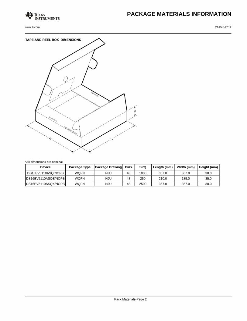
*All dimensions are nominal
Device Package Type Package Drawing Pins SPQ Length (mm) Width (mm) Height (mm)
DS16EV5110ASQ/NOPB WQFN NJU 48 1000 367.0 367.0 38.0
DS16EV5110ASQE/NOPB WQFN NJU 48 250 210.0 185.0 35.0
DS16EV5110ASQX/NOPB WQFN NJU 48 2500 367.0 367.0 38.0
PACKAGE MATERIALS INFORMATION
www.ti.com 21-Feb-2017
Pack Materials-Page 2

MECHANICAL DATA
NJU0048D
www.ti.com
SQA48D (Rev A)

IMPORTANT NOTICE
Texas Instruments Incorporated (TI) reserves the right to make corrections, enhancements, improvements and other changes to itssemiconductor products and services per JESD46, latest issue, and to discontinue any product or service per JESD48, latest issue. Buyersshould obtain the latest relevant information before placing orders and should verify that such information is current and complete.TI’s published terms of sale for semiconductor products (http://www.ti.com/sc/docs/stdterms.htm) apply to the sale of packaged integratedcircuit products that TI has qualified and released to market. Additional terms may apply to the use or sale of other types of TI products andservices.Reproduction of significant portions of TI information in TI data sheets is permissible only if reproduction is without alteration and isaccompanied by all associated warranties, conditions, limitations, and notices. TI is not responsible or liable for such reproduceddocumentation. Information of third parties may be subject to additional restrictions. Resale of TI products or services with statementsdifferent from or beyond the parameters stated by TI for that product or service voids all express and any implied warranties for theassociated TI product or service and is an unfair and deceptive business practice. TI is not responsible or liable for any such statements.Buyers and others who are developing systems that incorporate TI products (collectively, “Designers”) understand and agree that Designersremain responsible for using their independent analysis, evaluation and judgment in designing their applications and that Designers havefull and exclusive responsibility to assure the safety of Designers' applications and compliance of their applications (and of all TI productsused in or for Designers’ applications) with all applicable regulations, laws and other applicable requirements. Designer represents that, withrespect to their applications, Designer has all the necessary expertise to create and implement safeguards that (1) anticipate dangerousconsequences of failures, (2) monitor failures and their consequences, and (3) lessen the likelihood of failures that might cause harm andtake appropriate actions. Designer agrees that prior to using or distributing any applications that include TI products, Designer willthoroughly test such applications and the functionality of such TI products as used in such applications.TI’s provision of technical, application or other design advice, quality characterization, reliability data or other services or information,including, but not limited to, reference designs and materials relating to evaluation modules, (collectively, “TI Resources”) are intended toassist designers who are developing applications that incorporate TI products; by downloading, accessing or using TI Resources in anyway, Designer (individually or, if Designer is acting on behalf of a company, Designer’s company) agrees to use any particular TI Resourcesolely for this purpose and subject to the terms of this Notice.TI’s provision of TI Resources does not expand or otherwise alter TI’s applicable published warranties or warranty disclaimers for TIproducts, and no additional obligations or liabilities arise from TI providing such TI Resources. TI reserves the right to make corrections,enhancements, improvements and other changes to its TI Resources. TI has not conducted any testing other than that specificallydescribed in the published documentation for a particular TI Resource.Designer is authorized to use, copy and modify any individual TI Resource only in connection with the development of applications thatinclude the TI product(s) identified in such TI Resource. NO OTHER LICENSE, EXPRESS OR IMPLIED, BY ESTOPPEL OR OTHERWISETO ANY OTHER TI INTELLECTUAL PROPERTY RIGHT, AND NO LICENSE TO ANY TECHNOLOGY OR INTELLECTUAL PROPERTYRIGHT OF TI OR ANY THIRD PARTY IS GRANTED HEREIN, including but not limited to any patent right, copyright, mask work right, orother intellectual property right relating to any combination, machine, or process in which TI products or services are used. Informationregarding or referencing third-party products or services does not constitute a license to use such products or services, or a warranty orendorsement thereof. Use of TI Resources may require a license from a third party under the patents or other intellectual property of thethird party, or a license from TI under the patents or other intellectual property of TI.TI RESOURCES ARE PROVIDED “AS IS” AND WITH ALL FAULTS. TI DISCLAIMS ALL OTHER WARRANTIES ORREPRESENTATIONS, EXPRESS OR IMPLIED, REGARDING RESOURCES OR USE THEREOF, INCLUDING BUT NOT LIMITED TOACCURACY OR COMPLETENESS, TITLE, ANY EPIDEMIC FAILURE WARRANTY AND ANY IMPLIED WARRANTIES OFMERCHANTABILITY, FITNESS FOR A PARTICULAR PURPOSE, AND NON-INFRINGEMENT OF ANY THIRD PARTY INTELLECTUALPROPERTY RIGHTS. TI SHALL NOT BE LIABLE FOR AND SHALL NOT DEFEND OR INDEMNIFY DESIGNER AGAINST ANY CLAIM,INCLUDING BUT NOT LIMITED TO ANY INFRINGEMENT CLAIM THAT RELATES TO OR IS BASED ON ANY COMBINATION OFPRODUCTS EVEN IF DESCRIBED IN TI RESOURCES OR OTHERWISE. IN NO EVENT SHALL TI BE LIABLE FOR ANY ACTUAL,DIRECT, SPECIAL, COLLATERAL, INDIRECT, PUNITIVE, INCIDENTAL, CONSEQUENTIAL OR EXEMPLARY DAMAGES INCONNECTION WITH OR ARISING OUT OF TI RESOURCES OR USE THEREOF, AND REGARDLESS OF WHETHER TI HAS BEENADVISED OF THE POSSIBILITY OF SUCH DAMAGES.Unless TI has explicitly designated an individual product as meeting the requirements of a particular industry standard (e.g., ISO/TS 16949and ISO 26262), TI is not responsible for any failure to meet such industry standard requirements.Where TI specifically promotes products as facilitating functional safety or as compliant with industry functional safety standards, suchproducts are intended to help enable customers to design and create their own applications that meet applicable functional safety standardsand requirements. Using products in an application does not by itself establish any safety features in the application. Designers mustensure compliance with safety-related requirements and standards applicable to their applications. Designer may not use any TI products inlife-critical medical equipment unless authorized officers of the parties have executed a special contract specifically governing such use.Life-critical medical equipment is medical equipment where failure of such equipment would cause serious bodily injury or death (e.g., lifesupport, pacemakers, defibrillators, heart pumps, neurostimulators, and implantables). Such equipment includes, without limitation, allmedical devices identified by the U.S. Food and Drug Administration as Class III devices and equivalent classifications outside the U.S.TI may expressly designate certain products as completing a particular qualification (e.g., Q100, Military Grade, or Enhanced Product).Designers agree that it has the necessary expertise to select the product with the appropriate qualification designation for their applicationsand that proper product selection is at Designers’ own risk. Designers are solely responsible for compliance with all legal and regulatoryrequirements in connection with such selection.Designer will fully indemnify TI and its representatives against any damages, costs, losses, and/or liabilities arising out of Designer’s non-compliance with the terms and provisions of this Notice.
Mailing Address: Texas Instruments, Post Office Box 655303, Dallas, Texas 75265Copyright © 2017, Texas Instruments Incorporated