Embed Size (px)
Citation preview
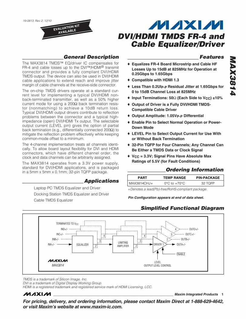
General DescriptionThe MAX3814 TMDS™ EQ/driver IC compensates for FR-4 and cable losses up to the DVI™/HDMI® transmitconnector and provides a fully compliant DVI/HDMITMDS output. The device can also be used in DVI/HDMIcable applications to extend reach and improve jittermargin of cable channels at the receive-side connector.
The on-chip TMDS drivers operate at a standard cur-rent level for implementing a typical DVI/HDMI non-back-terminated transmitter, as well as a 50% highercurrent mode for using a 200Ω back termination resis-tor (nonmatching) to achieve a 10dB return loss.Typical DVI/HDMI output drivers contribute to reflectionproblems between the connector and a typical high-impedance (open) DVI/HDMI Tx output. The selectableoutput current (LEVEL pin) gives the option of partialback termination (e.g., differentially connected 200Ω) tomitigate the reflection problem effectively while keepingcommon-mode offset to a minimum.
The 4-channel implementation treats all channels identi-cally. To allow board layout flexibility for DVI and HDMIconnectors, which have different channel order, theclock and data channels can be arbitrarily assigned.
The MAX3814 operates from a 3.3V power supply,standard for DVI/HDMI applications, and is packagedin a 5mm x 5mm x 0.1mm, 32-pin TQFP package.
ApplicationsLaptop PC TMDS Equalizer and Driver
Docking Station TMDS Equalizer and Driver
Cable TMDS Equalizer
Features♦ Equalizes FR-4 Board Microstrip and Cable HF
Losses Up to 15dB at 825MHz for Operation at0.25Gbps to 1.65Gbps
♦ Compatible with HDMI 1.3
♦ Less Than 0.2UIP-P Residual Jitter at 1.65Gbps for0 to 15dB Channel Loss at 825MHz
♦ Input Terminations: 50Ω (Each Side to VCC) ±10%
♦ Output of Driver is a Fully DVI/HDMI TMDS-Compatible Cable Driver
♦ Output Amplitude: 1.05VP-P Differential
♦ Enable Pin to Select Normal Operation or Power-Down Mode
♦ LEVEL Pin to Select Output Current for Use Withor Without Back Termination
♦ 32-Pin TQFP for Four Channels; Any Channel CanBe Either a TMDS Data or Clock Signal
♦ VCC = 3.3V; Signal Pins Have Absolute MaxRatings of 5.5V (for Fault Conditions)
MA
X3
81
4
DVI/HDMI TMDS FR-4 and Cable Equalizer/Driver
________________________________________________________________ Maxim Integrated Products 1
TERMINATED TO VCC
IND+/-
INC+/-
INB+/-
INA+/-
OUTD+/-
OUTC+/-
OUTB+/-
OUTA+/-
ENABLE
LEVELOUTPUT LEVEL CONTROLMAX3814
4
3
2EQUALIZER
1
4
3
2LIMITING
AMPLIFIER
1
4
3
2
DRIVER 1
Simplified Functional Diagram
Ordering InformationPART TEMP RANGE PIN-PACKAGE
MAX3814CHJ+ 0°C to +70°C 32 TQFP
19-0813; Rev 2; 12/10
For pricing, delivery, and ordering information, please contact Maxim Direct at 1-888-629-4642,or visit Maxim’s website at www.maxim-ic.com.
+Denotes a lead(Pb)-free/RoHS-compliant package.
TMDS is a trademark of Silicon Image, Inc.DVI is a trademark of Digital Display Working Group.HDMI is a registered trademark and registered service mark of HDMI Licensing, LCC.
EVALUATION KIT
AVAILABLE
Pin Configuration appears at end of data sheet.
MA
X3
81
4
DVI/HDMI TMDS FR-4 and Cable Equalizer/Driver
2 _______________________________________________________________________________________
ABSOLUTE MAXIMUM RATINGS
SPECIFICATION TABLES(Typical values measured at VCC = 3.3V, TA = +25°C; external terminations = 50Ω ±1%; min/max values valid over VCC = 3.3V±0.3V, TA = 0°C to +70°C; with external terminations = 50Ω ±1% to voltage = 3.3V ±0.7V. Tested at 1.65Gbps. AC parameters guar-anteed by design and characterization.)
POWER SUPPLY
Stresses beyond those listed under “Absolute Maximum Ratings” may cause permanent damage to the device. These are stress ratings only, and functionaloperation of the device at these or any other conditions beyond those indicated in the operational sections of the specifications is not implied. Exposure toabsolute maximum rating conditions for extended periods may affect device reliability.
Termination-Supply Voltage Range.......................-0.5V to +4.0VSignal Voltage Range on Any One Signal Wire ....-0.5V to +4.0VCML Common-Mode Voltage Range on
Any I/O Pair (sustained) .....................................-0.5V to +5.5VCML Common-Mode Voltage Range on Any I/O Pair
(sustained, within VCC and GND) ...-3.3V to +3.3V, Differential
CML Output Loading (termination)............................0Ω to OpenOperating Ambient Temperature Range ................0°C to +70°CStorage Ambient Temperature Range...............-40°C to +150°CESD Human Body Model, Any Pin .....................................2000VLead Temperature (soldering, 10s) .................................+300°CSoldering Temperature (reflow) .......................................+260°C
PARAMETER CONDITIONS MIN TYP MAX UNITS
DC PARAMETERS
Supply Current 110 140 mA
OPERATING CONDITIONSPARAMETER SYMBOL CONDITIONS MIN TYP MAX UNITS
Supply Voltage VCC 3.0 3.3 3.6 V
Operating Ambient Temperature 0 25 70 °C
Data Rate 0.25 1.65 Gbps
Maximum Channel Loss At 825MHz, FR-4 microstrip compensate on curve
15 dB
Source Output Rise/Fall Time 20% to 80%, measured at source transmitter (input to channel)
240 ps
Differential Input-Voltage Swing Measured at source transmitter (input to channel)
700 1050 1400 mVP-P
Maximum Supply Noise Tolerance
DC-5000kHz, all specifications maintained 50 mVP-P
TMDS EQUALIZER PERFORMANCEPARAMETER CONDITIONS MIN TYP MAX UNITS
Residual Output Jitter (15 x RJRMS + DJ) from 0.25Gbps to 1.65Gbps
Subtract source jitter for DJ, 0 to 15dB FR4 loss at 825MHz (Note 1)
0.2 UIP-P
MA
X3
81
4
DVI/HDMI TMDS FR-4 and Cable Equalizer/Driver
_______________________________________________________________________________________ 3
SPECIFICATION TABLES (continued)(Typical values measured at VCC = 3.3V, TA = +25°C; external terminations = 50Ω ±1%; min/max values valid over VCC = 3.3V±0.3V, TA = 0°C to +70°C; with external terminations = 50Ω ±1% to voltage = 3.3V ±0.7V. Tested at 1.65Gbps. AC parameters guar-anteed by design and characterization.)
CML INPUTSPARAMETER CONDITIONS MIN TYP MAX UNITS
DC PARAMETERS
Common-Mode Input VoltageVCC -400
VCC +100
mV
Input Termination Voltage When disconnected from sourceVCC -
10VCC +
10mV
Single-Ended Input Termination With 50Ω load, each side to VCC 45 50 55 ΩAC PARAMETERS
Differential Input Return Loss < 1.6GHz 14 dB
CML OUTPUTSPARAMETER CONDITIONS MIN TYP MAX UNITS
DC PARAMETERS
With 50Ω load, each side to VCC;LEVEL = low
900 1050 1200
Differential Output-Voltage SwingWith 50Ω load, each side to VCC;LEVEL = high; 200Ω back termination
900 1050 1200
mVP-P
Single-Ended High OutputVoltage
LEVEL = lowVCC -
10VCC +
10mV
Single-Ended Low OutputVoltage
LEVEL = lowVCC -600
VCC -400
mV
Output Voltage When ENABLEDisabled
LEVEL = low, ENABLE = highVCC -
10VCC +
10mV
AC PARAMETERS
Output, Rise/Fall Time20% to 80%; with 50Ω load,each side to VCC
80 170 230 ps
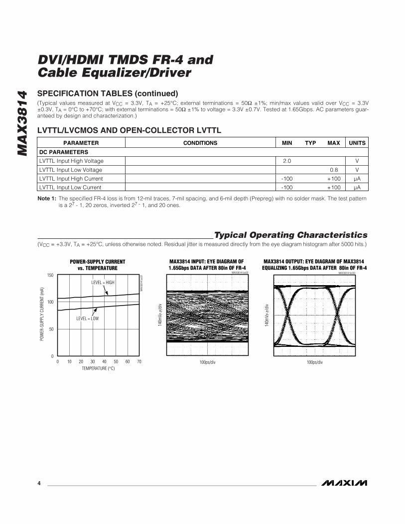
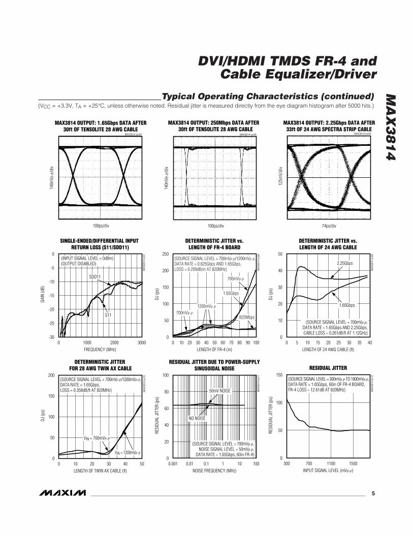
Typical Operating Characteristics(VCC = +3.3V, TA = +25°C, unless otherwise noted. Residual jitter is measured directly from the eye diagram histogram after 5000 hits.)
MA
X3
81
4
DVI/HDMI TMDS FR-4 and Cable Equalizer/Driver
4 _______________________________________________________________________________________
Note 1: The specified FR-4 loss is from 12-mil traces, 7-mil spacing, and 6-mil depth (Prepreg) with no solder mask. The test patternis a 27 - 1, 20 zeros, inverted 27 - 1, and 20 ones.
LVTTL/LVCMOS AND OPEN-COLLECTOR LVTTL
PARAMETER CONDITIONS MIN TYP MAX UNITS
DC PARAMETERS
LVTTL Input High Voltage 2.0 V
LVTTL Input Low Voltage 0.8 V
LVTTL Input High Current -100 +100 μA
LVTTL Input Low Current -100 +100 μA
POWER-SUPPLY CURRENTvs. TEMPERATURE
MAX
3814
toc0
1
TEMPERATURE (°C)
POW
ER-S
UPPL
Y CU
RREN
T (m
A)
605040302010
50
100
150
00 70
LEVEL = HIGH
LEVEL = LOW
MAX3814 INPUT: EYE DIAGRAM OF 1.65Gbps DATA AFTER 80in OF FR-4
MAX3814 toc02
100ps/div
140m
V P-P
/div
MAX3814 toc03
MAX3814 OUTPUT: EYE DIAGRAM OF MAX3814 EQUALIZING 1.65Gbps DATA AFTER 80in OF FR-4
100ps/div
140m
V P-P
/div
SPECIFICATION TABLES (continued)(Typical values measured at VCC = 3.3V, TA = +25°C; external terminations = 50Ω ±1%; min/max values valid over VCC = 3.3V±0.3V, TA = 0°C to +70°C; with external terminations = 50Ω ±1% to voltage = 3.3V ±0.7V. Tested at 1.65Gbps. AC parameters guar-anteed by design and characterization.)
MA
X3
81
4
DVI/HDMI TMDS FR-4 and Cable Equalizer/Driver
_______________________________________________________________________________________ 5
MAX3814 toc04
MAX3814 OUTPUT: 1.65Gbps DATA AFTER30ft OF TENSOLITE 28 AWG CABLE
100ps/div
140m
V P-P
/div
MAX3814 toc05
MAX3814 OUTPUT: 250Mbps DATA AFTER 30ft OF TENSOLITE 28 AWG CABLE
100ps/div
140m
V P-P
/div
MAX3814 OUTPUT: 2.25Gbps DATA AFTER33ft OF 24 AWG SPECTRA STRIP CABLE
MAX3814 toc06
74ps/div
125m
V/di
v
Typical Operating Characteristics (continued)(VCC = +3.3V, TA = +25°C, unless otherwise noted. Residual jitter is measured directly from the eye diagram histogram after 5000 hits.)
SINGLE-ENDED/DIFFERENTIAL INPUT RETURN LOSS (S11/SDD11)
MAX
3814
toc0
7
FREQUENCY (MHz)
GAIN
(dB)
20001000
-25
-20
-15
-10
-5
0
-300 3000
(INPUT SIGNAL LEVEL = 0dBm)(OUTPUT DISABLED)
SDD11
S11
DETERMINISTIC JITTER vs.LENGTH OF FR-4 BOARD
MAX
3814
toc0
8
LENGTH OF FR-4 (in)
DJ (p
s)
908070605040302010
50
100
150
200
250
00 100
(SOURCE SIGNAL LEVEL = 700mVP-P/1200mVP-P,DATA RATE = 0.825Gbps AND 1.65Gbps,LOSS = 0.209dB/in AT 820MHz)
700mVP-P
1200mVP-P
1.65Gbps
825Mbps
700mVP-P
DETERMINISTIC JITTER vs.LENGTH OF 24 AWG CABLE
MAX
3814
toc0
9
LENGTH OF 24 AWG CABLE (ft)
DJ (p
s)
3530252015105
10
20
30
40
50
00 40
1.65Gbps
(SOURCE SIGNAL LEVEL = 700mVP-P,DATA RATE = 1.65Gbps AND 2.25Gbps,CABLE LOSS = 0.261dB/ft AT 1.12GHz)
2.25Gbps
DETERMINISTIC JITTER FOR 28 AWG TWIN AX CABLE
MAX
3814
toc1
0
LENGTH OF TWIN AX CABLE (ft)
DJ (p
s)
40302010
50
100
150
200
00 50
VIN = 700mVP-P
VIN = 1200mVP-P
(SOURCE SIGNAL LEVEL = 700mVP-P/1200mVP-P,DATA RATE = 1.65Gbps,LOSS = 0.358dB/ft AT 820MHz)
RESIDUAL JITTER DUE TO POWER-SUPPLYSINUSOIDAL NOISE
MAX
3814
toc1
1
NOISE FREQUENCY (MHz)
RESI
DUAL
JITT
ER (p
s)
1010.10.01
20
40
60
80
100
00.001 100
NO NOISE
50mV NOISE
(SOURCE SIGNAL LEVEL = 700mVP-P,NOISE SIGNAL LEVEL = 50mVP-P,
DATA RATE = 1.65Gbps, 60in FR-4)
RESIDUAL JITTERM
AX38
14 to
c12
INPUT SIGNAL LEVEL (mVP-P)
RESI
DUAL
JITT
ER (p
s)
15001100700
50
100
150
0300
(SOURCE SIGNAL LEVEL = 300mVP-P TO 1800mVP-P,DATA RATE = 1.65Gbps, 60in OF FR-4 BOARD,FR-4 LOSS = 12.61dB AT 820MHz)
MA
X3
81
4
DVI/HDMI TMDS FR-4 and Cable Equalizer/Driver
6 _______________________________________________________________________________________
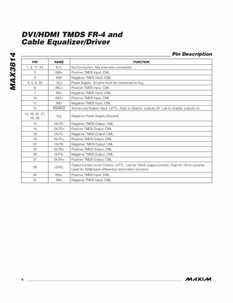
Pin DescriptionPIN NAME FUNCTION
1, 8, 17, 24 N.C. No Connection. Not internally connected.
2 INB+ Positive TMDS Input, CML
3 INB- Negative TMDS Input, CML
4, 5, 9, 32 VCC Power Supply. All pins must be connected to VCC.
6 INC+ Positive TMDS Input, CML
7 INC- Negative TMDS Input, CML
10 IND+ Positive TMDS Input, CML
11 IND- Negative TMDS Input, CML
12 ENABLE Active-Low Enable Input, LVTTL. High to disable, outputs off. Low to enable, outputs on.
13, 16, 20, 21, 25, 28
VEE Negative Power Supply (Ground)
14 OUTD- Negative TMDS Output, CML
15 OUTD+ Positive TMDS Output, CML
18 OUTC- Negative TMDS Output, CML
19 OUTC+ Positive TMDS Output, CML
22 OUTB- Negative TMDS Output, CML
23 OUTB+ Positive TMDS Output, CML
26 OUTA- Negative TMDS Output, CML
27 OUTA+ Positive TMDS Output, CML
29 LEVEL Output Current Level Control, LVTTL. Low for 10mA output currents. High for 15mA currents. Used for 200 back differential termination resistors.
30 INA+ Positive TMDS Input, CML
31 INA- Negative TMDS Input, CML
MA
X3
81
4
DVI/HDMI TMDS FR-4 and Cable Equalizer/Driver
_______________________________________________________________________________________ 7
DRIVEREQUALIZER LIMITINGAMPLIFIER
TERMINATEDTO VCC
DRIVEREQUALIZER LIMITINGAMPLIFIER
TERMINATEDTO VCC
DRIVEREQUALIZER
EQUALIZER
LIMITINGAMPLIFIER
TERMINATEDTO VCC
DRIVERLIMITINGAMPLIFIER
TERMINATEDTO VCC
OUTD+/-
LEVELOUTPUT LEVEL CONTROL
OUTC+/-
OUTB+/-
OUTA+/-INA+/-
INB+/-
INC+/-
IND+/-
ENABLE
MAX3814
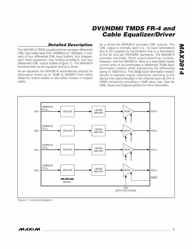
Detailed DescriptionThe MAX3814 TMDS equalizer/driver accepts differentialCML input data rates from 250Mbps to 1.65Gbps. It con-sists of four differential CML input buffers, four indepen-dent fixed equalizers, four limiting amplifiers, and fourdifferential CML output buffers (Figure 1). The MAX3814functions both as an equalizer and as a driver.
As an equalizer the MAX3814 automatically adjusts forattenuation levels up to 16dB at 825MHz from eitherdielectric board losses or skin-effect losses in coppercable.
As a driver the MAX3814 provides CML outputs. TheCML output is normally open (i.e., no back termination)and is DC-coupled by transmission line to a terminationat the far end per DVI/HDMI standards. The MAX3814provides nominally 10mA output-switching currents.However, with the MAX3814, there is a selectable highercurrent drive to accommodate a differential 200Ω backtermination resistor while maintaining the differentialswing of 1000mVP-P. This 200Ω back termination resistorserves to dampen signal reflections returning to thedevice from discontinuities in the channel such as DVI orHDMI connectors, providing a 10dB return loss. See theCML Inputs and Outputs section for more information.
Figure 1. Functional Diagram
MA
X3
81
4
DVI/HDMI TMDS FR-4 and Cable Equalizer/Driver
8 _______________________________________________________________________________________
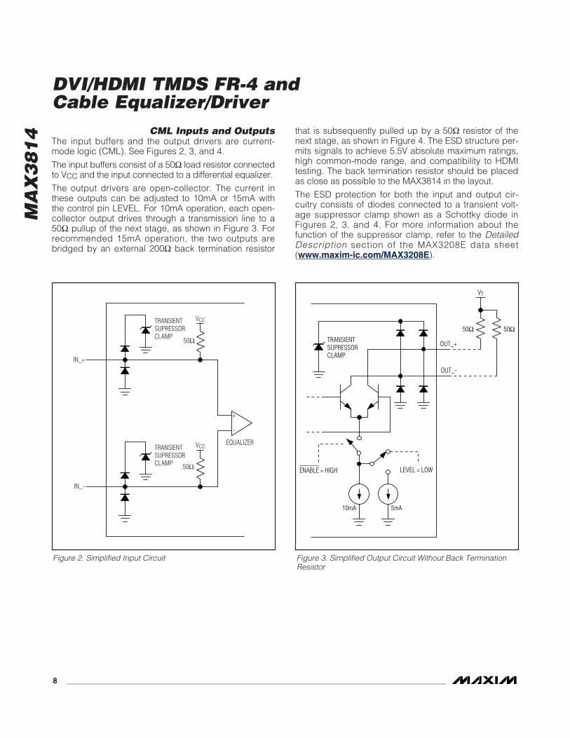
CML Inputs and OutputsThe input buffers and the output drivers are current-mode logic (CML). See Figures 2, 3, and 4.
The input buffers consist of a 50Ω load resistor connectedto VCC and the input connected to a differential equalizer.
The output drivers are open-collector. The current inthese outputs can be adjusted to 10mA or 15mA withthe control pin LEVEL. For 10mA operation, each open-collector output drives through a transmission line to a50Ω pullup of the next stage, as shown in Figure 3. Forrecommended 15mA operation, the two outputs arebridged by an external 200Ω back termination resistor
that is subsequently pulled up by a 50Ω resistor of thenext stage, as shown in Figure 4. The ESD structure per-mits signals to achieve 5.5V absolute maximum ratings,high common-mode range, and compatibility to HDMItesting. The back termination resistor should be placedas close as possible to the MAX3814 in the layout.
The ESD protection for both the input and output cir-cuitry consists of diodes connected to a transient volt-age suppressor clamp shown as a Schottky diode inFigures 2, 3, and 4. For more information about thefunction of the suppressor clamp, refer to the DetailedDescription section of the MAX3208E data sheet(www.maxim-ic.com/MAX3208E).
EQUALIZERTRANSIENTSUPRESSORCLAMP
VCC
VCC
IN_+
IN_-
50Ω
50Ω
+
-
TRANSIENTSUPRESSORCLAMP
Figure 2. Simplified Input Circuit
5mA
50Ω50Ω
ENABLE = HIGH LEVEL = LOW
VT
TRANSIENTSUPRESSORCLAMP
10mA
OUT_+
OUT_-
Figure 3. Simplified Output Circuit Without Back TerminationResistor
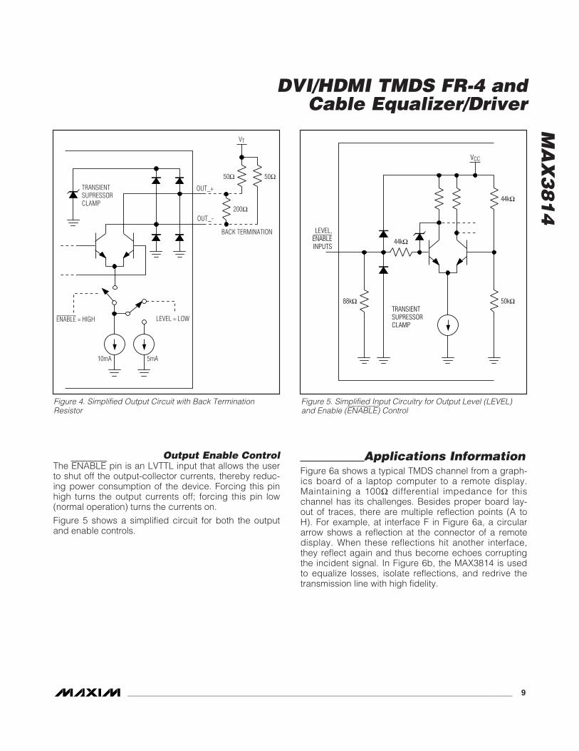
Output Enable ControlThe ENABLE pin is an LVTTL input that allows the userto shut off the output-collector currents, thereby reduc-ing power consumption of the device. Forcing this pinhigh turns the output currents off; forcing this pin low(normal operation) turns the currents on.
Figure 5 shows a simplified circuit for both the outputand enable controls.
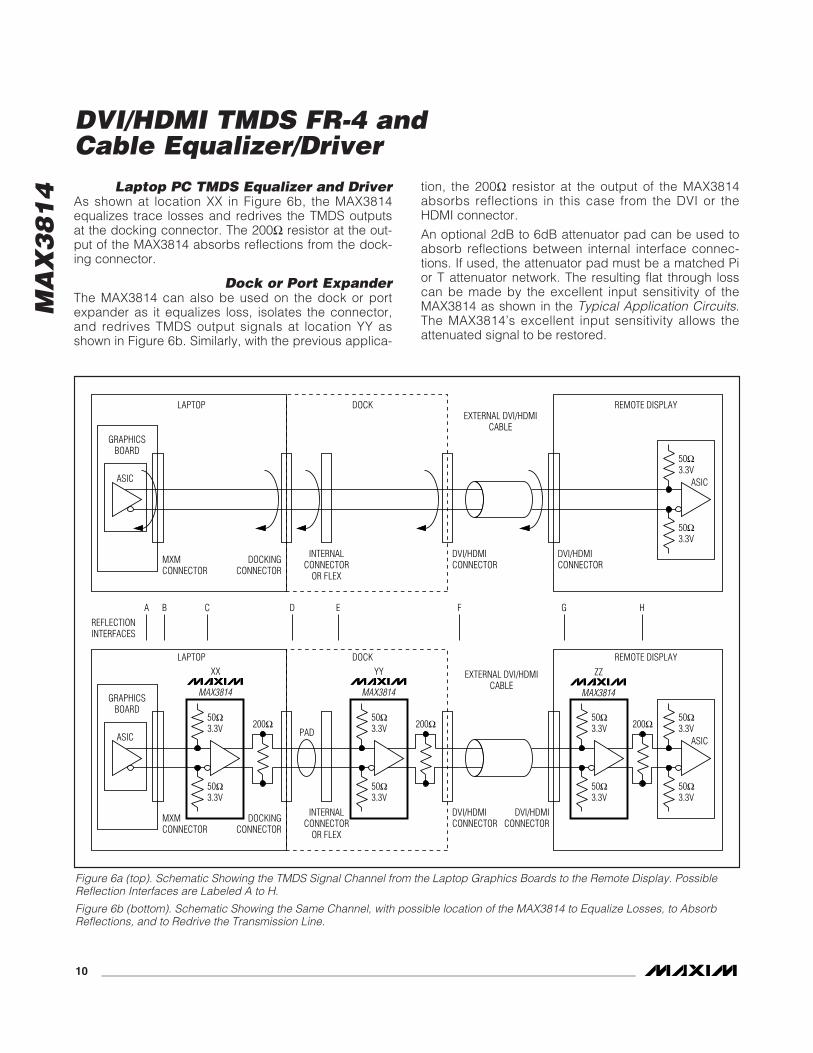
Applications InformationFigure 6a shows a typical TMDS channel from a graph-ics board of a laptop computer to a remote display.Maintaining a 100Ω differential impedance for thischannel has its challenges. Besides proper board lay-out of traces, there are multiple reflection points (A toH). For example, at interface F in Figure 6a, a circulararrow shows a reflection at the connector of a remotedisplay. When these reflections hit another interface,they reflect again and thus become echoes corruptingthe incident signal. In Figure 6b, the MAX3814 is usedto equalize losses, isolate reflections, and redrive thetransmission line with high fidelity.
MA
X3
81
4
DVI/HDMI TMDS FR-4 and Cable Equalizer/Driver
_______________________________________________________________________________________ 9
50Ω
200Ω
BACK TERMINATION
50Ω
VT
TRANSIENTSUPRESSORCLAMP
OUT_+
OUT_-
5mA
ENABLE = HIGH LEVEL = LOW
10mA
Figure 4. Simplified Output Circuit with Back TerminationResistor
TRANSIENTSUPRESSORCLAMP
50kΩ
44kΩ
VCC
44kΩ
88kΩ
LEVEL,ENABLEINPUTS
Figure 5. Simplified Input Circuitry for Output Level (LEVEL)and Enable (ENABLE) Control
MA
X3
81
4 Laptop PC TMDS Equalizer and DriverAs shown at location XX in Figure 6b, the MAX3814equalizes trace losses and redrives the TMDS outputsat the docking connector. The 200Ω resistor at the out-put of the MAX3814 absorbs reflections from the dock-ing connector.
Dock or Port ExpanderThe MAX3814 can also be used on the dock or portexpander as it equalizes loss, isolates the connector,and redrives TMDS output signals at location YY asshown in Figure 6b. Similarly, with the previous applica-
tion, the 200Ω resistor at the output of the MAX3814absorbs reflections in this case from the DVI or theHDMI connector.
An optional 2dB to 6dB attenuator pad can be used toabsorb reflections between internal interface connec-tions. If used, the attenuator pad must be a matched Pior T attenuator network. The resulting flat through losscan be made by the excellent input sensitivity of theMAX3814 as shown in the Typical Application Circuits.The MAX3814’s excellent input sensitivity allows theattenuated signal to be restored.
DVI/HDMI TMDS FR-4 and Cable Equalizer/Driver
10 ______________________________________________________________________________________
LAPTOP
A
DOCKEXTERNAL DVI/HDMI
CABLE
DVI/HDMICONNECTOR
DVI/HDMICONNECTORMXM
CONNECTOR
REFLECTIONINTERFACES
DOCKINGCONNECTOR
INTERNALCONNECTOR
OR FLEX
REMOTE DISPLAY
GRAPHICSBOARD
ASIC ASIC
50Ω3.3V
50Ω3.3V
LAPTOP DOCK
EXTERNAL DVI/HDMICABLE
DVI/HDMICONNECTOR
DVI/HDMICONNECTORMXM
CONNECTORDOCKING
CONNECTOR
INTERNALCONNECTOR
OR FLEX
REMOTE DISPLAY
GRAPHICSBOARD
ASIC ASIC
200Ω50Ω3.3V
50Ω3.3V
50Ω3.3V
50Ω3.3V
50Ω3.3V
50Ω3.3V
200Ω50Ω3.3V
50Ω3.3V
200ΩPAD
B C D E F G H
MAX3814
XX
MAX3814
YY
MAX3814
ZZ
Figure 6a (top). Schematic Showing the TMDS Signal Channel from the Laptop Graphics Boards to the Remote Display. PossibleReflection Interfaces are Labeled A to H.
Figure 6b (bottom). Schematic Showing the Same Channel, with possible location of the MAX3814 to Equalize Losses, to AbsorbReflections, and to Redrive the Transmission Line.
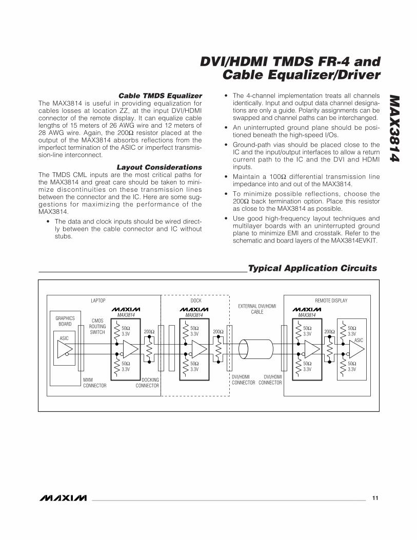
Cable TMDS EqualizerThe MAX3814 is useful in providing equalization forcables losses at location ZZ, at the input DVI/HDMIconnector of the remote display. It can equalize cablelengths of 15 meters of 26 AWG wire and 12 meters of28 AWG wire. Again, the 200Ω resistor placed at theoutput of the MAX3814 absorbs reflections from theimperfect termination of the ASIC or imperfect transmis-sion-line interconnect.
Layout ConsiderationsThe TMDS CML inputs are the most critical paths forthe MAX3814 and great care should be taken to mini-mize discontinuities on these transmission linesbetween the connector and the IC. Here are some sug-gestions for maximizing the performance of theMAX3814.
• The data and clock inputs should be wired direct-ly between the cable connector and IC withoutstubs.
• The 4-channel implementation treats all channelsidentically. Input and output data channel designa-tions are only a guide. Polarity assignments can beswapped and channel paths can be interchanged.
• An uninterrupted ground plane should be posi-tioned beneath the high-speed I/Os.
• Ground-path vias should be placed close to theIC and the input/output interfaces to allow a returncurrent path to the IC and the DVI and HDMIinputs.
• Maintain a 100Ω differential transmission lineimpedance into and out of the MAX3814.
• To minimize possible reflections, choose the200Ω back termination option. Place this resistoras close to the MAX3814 as possible.
• Use good high-frequency layout techniques andmultilayer boards with an uninterrupted groundplane to minimize EMI and crosstalk. Refer to theschematic and board layers of the MAX3814EVKIT.
MA
X3
81
4
DVI/HDMI TMDS FR-4 and Cable Equalizer/Driver
______________________________________________________________________________________ 11
LAPTOP DOCKEXTERNAL DVI/HDMI
CABLE
DVI/HDMICONNECTOR
DVI/HDMICONNECTORMXM
CONNECTORDOCKING
CONNECTOR
REMOTE DISPLAY
GRAPHICSBOARD
ASIC ASIC
200Ω50Ω3.3V
50Ω3.3V
50Ω3.3V
50Ω3.3V
50Ω3.3V
50Ω3.3V
200Ω
CMOSROUTINGSWITCH
50Ω3.3V
50Ω3.3V
200Ω
MAX3814 MAX3814 MAX3814
Typical Application Circuits
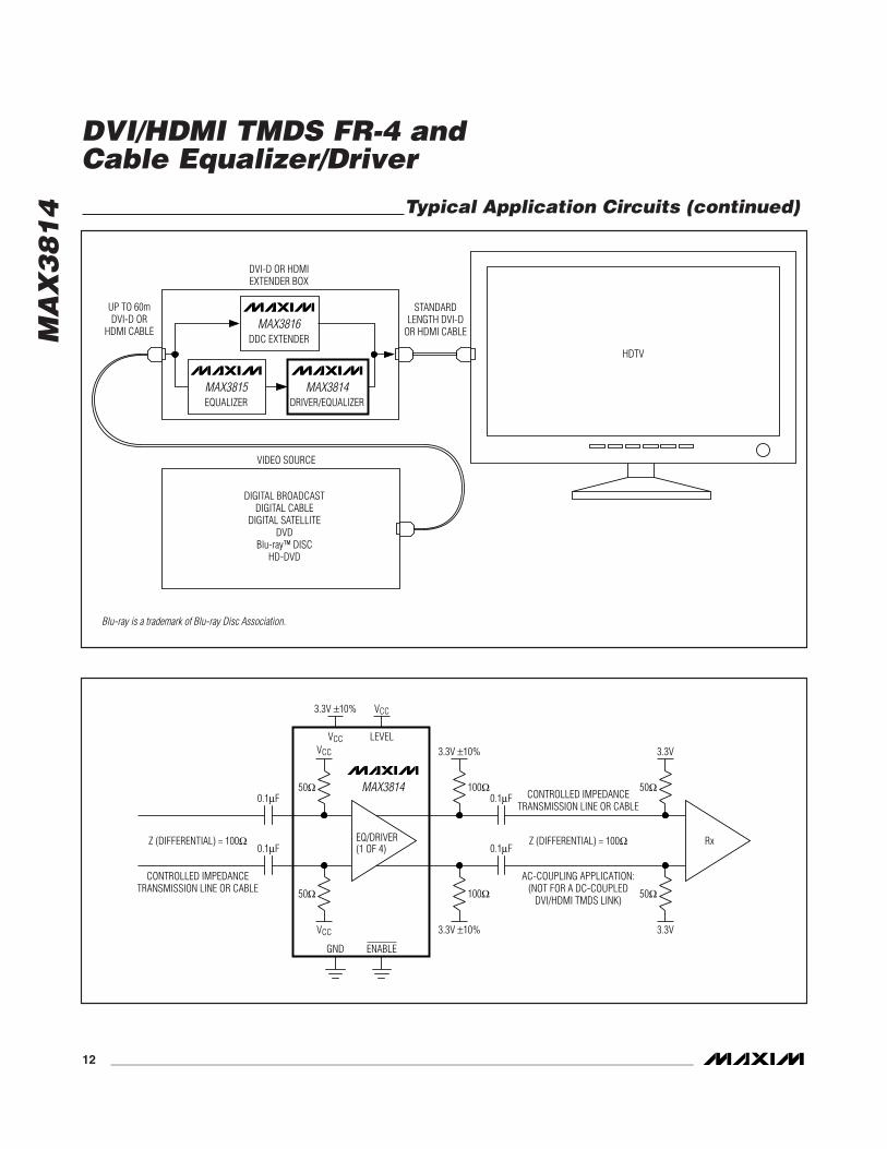
MAX3814DRIVER/EQUALIZER
MAX3816DDC EXTENDER
MAX3815EQUALIZER
HDTV
UP TO 60mDVI-D OR
HDMI CABLE
STANDARDLENGTH DVI-D
OR HDMI CABLE
DIGITAL BROADCASTDIGITAL CABLE
DIGITAL SATELLITEDVD
Blu-ray™ DISCHD-DVD
Blu-ray is a trademark of Blu-ray Disc Association.
DVI-D OR HDMIEXTENDER BOX
VIDEO SOURCE
Typical Application Circuits (continued)
MA
X3
81
4
DVI/HDMI TMDS FR-4 and Cable Equalizer/Driver
12 ______________________________________________________________________________________
MAX3814
EQ/DRIVER
VCC
3.3V ±10%
VCC
VCC
LEVEL
50Ω0.1μF
0.1μF
0.1μF
0.1μFZ (DIFFERENTIAL) = 100Ω
AC-COUPLING APPLICATION:(NOT FOR A DC-COUPLED
DVI/HDMI TMDS LINK)
CONTROLLED IMPEDANCETRANSMISSION LINE OR CABLE
CONTROLLED IMPEDANCETRANSMISSION LINE OR CABLE
Z (DIFFERENTIAL) = 100Ω
50Ω
VCC
Rx
3.3V
50Ω
50Ω
3.3V
3.3V ±10%
100Ω
100Ω
3.3V ±10%
ENABLEGND
(1 OF 4)
MA
X3
81
4
DVI/HDMI TMDS FR-4 and Cable Equalizer/Driver
______________________________________________________________________________________ 13
Chip InformationPROCESS: SiGe BiPOLAR
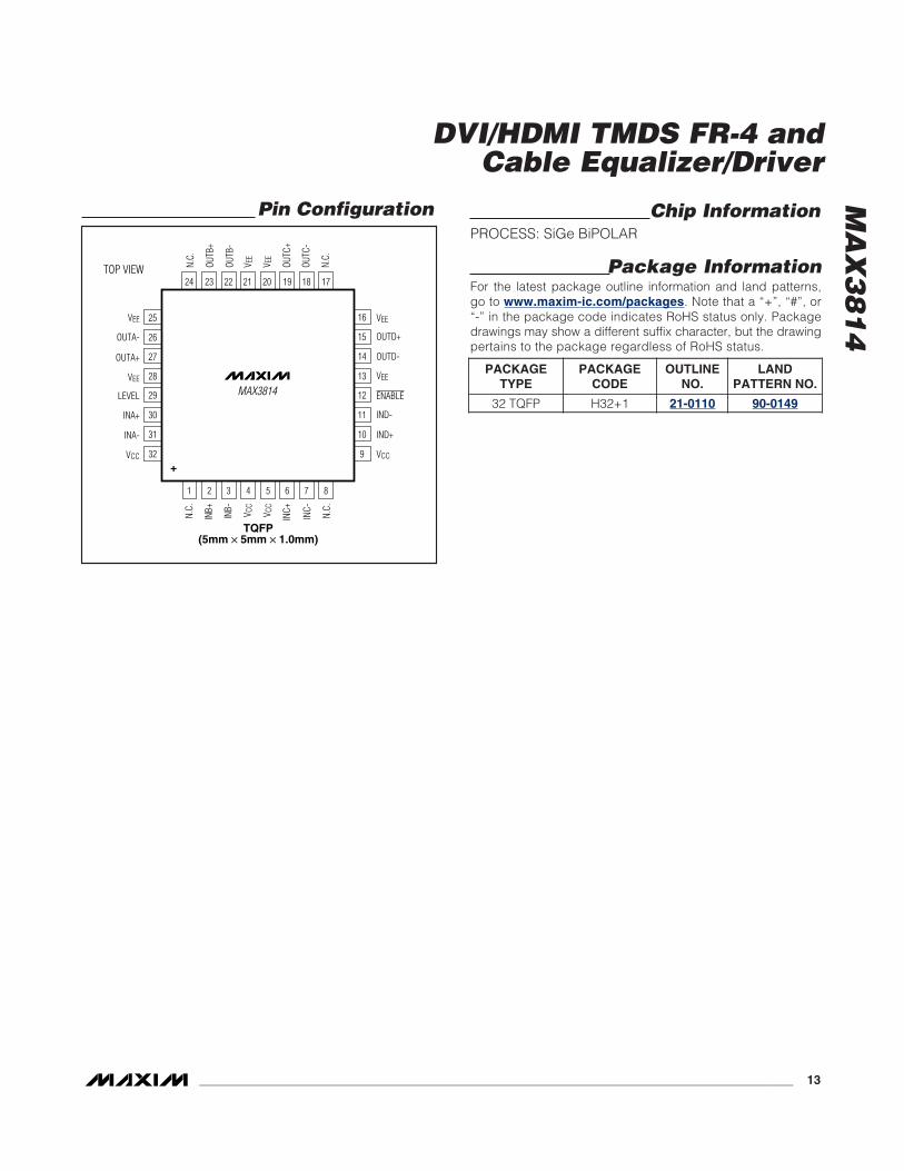
Package InformationFor the latest package outline information and land patterns,go to www.maxim-ic.com/packages. Note that a “+”, “#”, or“-” in the package code indicates RoHS status only. Packagedrawings may show a different suffix character, but the drawingpertains to the package regardless of RoHS status.
MAX3814
TQFP(5mm × 5mm × 1.0mm)
TOP VIEW
29
30
28
27
12
11
13
INB+ V C
C
V CC
INC+
INC-
14
N.C.
OUTB
+
V EE
V EE
N.C.
OUTC
+
OUTC
-
1
+
2
VEE
4 5 6 7
2324 22 20 19 18
LEVEL
INA+
OUTD-
VEE
ENABLE
IND-
INB-
OUTB
-
3
21
31 10INA- IND+
32 9VCC VCC
OUTA+
26 15 OUTD+OUTA-
25 16 VEEN.
C.N.
C.
8
17
VEE
Pin Configuration
PACKAGETYPE
PACKAGECODE
OUTLINENO.
LANDPATTERN NO.
32 TQFP H32+1 21-0110 90-0149
MA
X3
81
4
DVI/HDMI TMDS FR-4 and Cable Equalizer/Driver
Maxim cannot assume responsibility for use of any circuitry other than circuitry entirely embodied in a Maxim product. No circuit patent licenses areimplied. Maxim reserves the right to change the circuitry and specifications without notice at any time.
14 ____________________Maxim Integrated Products, 120 San Gabriel Drive, Sunnyvale, CA 94086 408-737-7600
© 2010 Maxim Integrated Products Maxim is a registered trademark of Maxim Integrated Products, Inc.
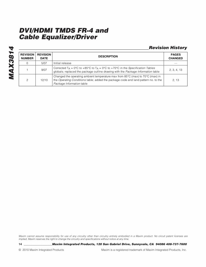
Revision HistoryREVISION NUMBER
REVISION DATE
DESCRIPTION PAGES
CHANGED
0 5/07 Initial release —
1 9/07 Corrected TA = 0°C to +85°C to TA = 0°C to +70°C in the Specification Tablesglobals; replaced the package outline drawing with the Package Information table
2, 3, 4, 13
2 12/10 Changed the operating ambient temperature max from 85°C (max) to 70°C (max) in the Operating Conditions table; added the package code and land pattern no. to the Package Information table
2, 13