Embed Size (px)
Citation preview
1113/Engg/SE/Pre Pap/2013/CMPN/ECCF_Soln 1
Vidyalankar S.E. Sem. III [CMPN]
Electronic Circuits and Communication Fundamentals Prelim Question Paper Solution
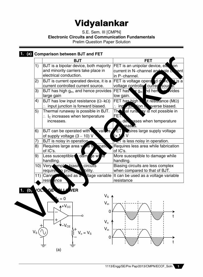
Comparison between BJT and FET
BJT FET 1) BJT is a bipolar device, both majority
and minority carriers take place in electrical conduction.
FET is an unipolar device, electron current in Nchannel and hole current in Pchannel.
2) BJT is current operated device, it is a current controlled current source.
FET is voltage operated device, it is a voltage controlled current source.
3) BJT has high gm, and hence provides large gain
FET has low gm and hence provides low gain.
4) BJT has low input resistance (k) input junction is forward biased.
FET has high input resistance (M) input junction is reverse biased.
5) Thermal runaway is possible in BJT. IC increases when temperature
increases.
Thermal runaway is not possible in FET. ID decreases when temperature
increases. 6) BJT can be operated with low values
of supply voltage (3 10) V FET requires large supply voltage (> 10) V
7) BJT is noisy in operation. FET is less noisy in operation. 8) Requires large area while fabrication
of IC's. Requires less area while fabrication of IC's.
9) Less susceptible to damage while handling.
More susceptible to damage while handling.
10) Very complex biasing circuits required to provide stability.
Biasing circuits are less complex when compared to that of BJT.
11) Cannot be used as a voltage variable resistance
It can be used as a voltage variable resistance
VOLTAGE-FOLLOWER
1. (a)
1. (b)
+VCC
–VCE
Vo = VS VS
RF = 0
(a)
Vin
t 0
VS
Vin
t 0
Vo Vidyala
nkar

Vidyalankar : S.E. – ECCF
1113/Engg/SE/Pre Pap/2013/CMPN/ECCF_Soln 2
When R1 = and RF = 0 the non-inverting amplifier gets converted into a voltage follower or unity gain amplifier. When non-inverting amplifier is configured so as to obtain a gain of 1, it is called as voltage follower or unity gain non-inverting buffer. The schematic diagram for voltage follower is a shown below. The voltage follower configuration in figure (a) is obtained by short circuiting RF and open circuiting R1 connected in usual non-inverting amplifier configuration in figure (a). Thus all the output is feedback to inverting input of OP-AMP. Therefore the gain of feedback circuit i.e. B = 1 OPERATIONAL AMPLIFIER Block diagram The input stage is a dual input balanced output high gain differential amplifier, and has a very high input resistance. This is done by making use of darlington connection or by FET as input stage. The output of the 1st differential amplifier is used to drive dual input unbalanced output differential amplifier. Because of direct coupling, the dc voltage at the output of intermediate stage is above ground potential. Therefore a level shifter is used at the output of 2nd stage to shift the dc level at the output of the intermediate stage down to zero with respect to ground. The level translator is an emitter follower using constant current bias. The final stage is a push pull complementary symmetry amplifier, which increases the output voltage swing and increases the current supplying capability of opamp. First stage : Consists of transistors, which form the first differential amplifier stage, using constant current bias provided by transistor at the emitter and associated resistances. This 1st stage has inverting and non-inverting input and hence can be driven with two input's or a single input. The 1st stage establishes. i) high input resistance ii) high voltage gain iii) rejects common signals iv) eliminates drift v) provides high CMRR
1. (c)
VCC
Vee
V1 V2
V0
Q1 Q2
Q3
Q4
input stage
+
2nd Stage
Level
Translator
output stage
output i/p
IN
NI dual i/p
balanced o/p diff. amplifier
dual i/p unbalanced o/p
diff. amplifier
emitter follower with constant current bias
Complementary symmetry
class AB amplifier
Vidyala
nkar
Prelim Question Paper Solution
1113/Engg/SE/Pre Pap/2013/CMPN/ECCF_Soln 3
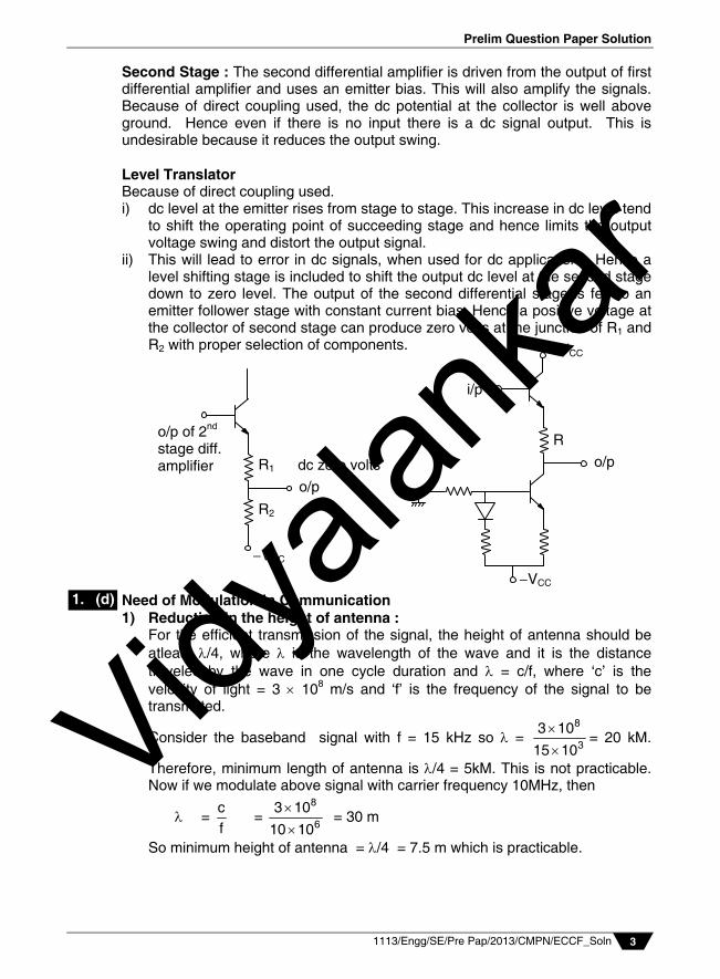
Second Stage : The second differential amplifier is driven from the output of first differential amplifier and uses an emitter bias. This will also amplify the signals. Because of direct coupling used, the dc potential at the collector is well above ground. Hence even if there is no input there is a dc signal output. This is undesirable because it reduces the output swing. Level Translator Because of direct coupling used. i) dc level at the emitter rises from stage to stage. This increase in dc level tend
to shift the operating point of succeeding stage and hence limits the output voltage swing and distort the output signal.
ii) This will lead to error in dc signals, when used for dc applications. Hence a level shifting stage is included to shift the output dc level at the second stage down to zero level. The output of the second differential stage is fed to an emitter follower stage with constant current bias. Hence a positive voltage at the collector of second stage can produce zero volts at the junction of R1 and R2 with proper selection of components.
Need of Modulation in Communication 1) Reduction in the height of antenna : For the efficient transmission of the signal, the height of antenna should be
atleast /4, where is the wavelength of the wave and it is the distance traveled by the wave in one cycle duration and = c/f, where ‘c’ is the velocity of light = 3 108 m/s and ‘f’ is the frequency of the signal to be transmitted.
Consider the baseband signal with f = 15 kHz so = 8
3
3 10
15 10
= 20 kM.
Therefore, minimum length of antenna is /4 = 5kM. This is not practicable. Now if we modulate above signal with carrier frequency 10MHz, then
= cf
= 8
6
3 10
10 10
= 30 m
So minimum height of antenna = /4 = 7.5 m which is practicable.
1. (d)
R1
R2
VCC
o/p of 2nd stage diff. amplifier
o/p
dc zero volts
VCC
o/p
R
+VCC
i/p
Vidyala
nkar
Vidyalankar : S.E. – ECCF
1113/Engg/SE/Pre Pap/2013/CMPN/ECCF_Soln 4
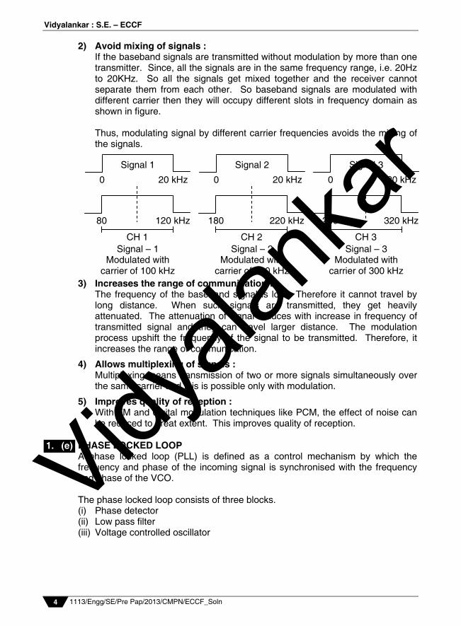
2) Avoid mixing of signals : If the baseband signals are transmitted without modulation by more than one
transmitter. Since, all the signals are in the same frequency range, i.e. 20Hz to 20KHz. So all the signals get mixed together and the receiver cannot separate them from each other. So baseband signals are modulated with different carrier then they will occupy different slots in frequency domain as shown in figure.
Thus, modulating signal by different carrier frequencies avoids the mixing of
the signals. 3) Increases the range of communication : The frequency of the baseband signal is low. Therefore it cannot travel by
long distance. When such signals are transmitted, they get heavily attenuated. The attenuation of signal reduces with increase in frequency of transmitted signal and they can travel larger distance. The modulation process upshift the frequency of the signal to be transmitted. Therefore, it increases the range of communication.
4) Allows multiplexing of signals : Multiplexing means transmission of two or more signals simultaneously over
the same carrier and this is possible only with modulation.
5) Improves quality of reception : With FM and digital modulation techniques like PCM, the effect of noise can
be reduced to great extent. This improves quality of reception. PHASE LOCKED LOOP A phase locked loop (PLL) is defined as a control mechanism by which the frequency and phase of the incoming signal is synchronised with the frequency and phase of the VCO. The phase locked loop consists of three blocks. (i) Phase detector (ii) Low pass filter (iii) Voltage controlled oscillator
1. (e)
Signal 1
0 20 kHz
CH 1
80 120 kHz
Signal – 1 Modulated with
carrier of 100 kHz
Signal 2
0 20 kHz
CH 2
180 220 kHz
Signal – 2 Modulated with
carrier of 200 kHz
Signal 3
0 20 kHz
CH 3
280 320 kHz
Signal – 3 Modulated with
carrier of 300 kHz
Vidyala
nkar
Prelim Question Paper Solution
1113/Engg/SE/Pre Pap/2013/CMPN/ECCF_Soln 5
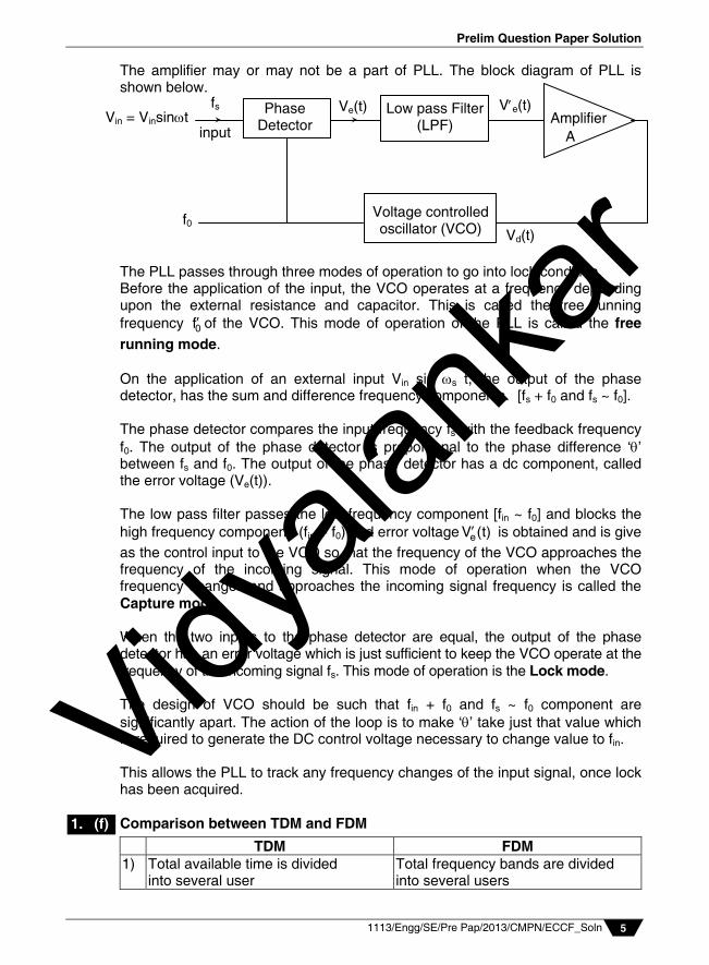
The amplifier may or may not be a part of PLL. The block diagram of PLL is shown below. The PLL passes through three modes of operation to go into lock condition. Before the application of the input, the VCO operates at a frequency depending upon the external resistance and capacitor. This is called the free running frequency 0f of the VCO. This mode of operation of the PLL is called the free running mode. On the application of an external input Vin sin s t, the output of the phase detector, has the sum and difference frequency components. [fs + f0 and fs ~ f0]. The phase detector compares the input frequency fs with the feedback frequency f0. The output of the phase detector is proportional to the phase difference ‘’ between fs and f0. The output of the phase detector has a dc component, called the error voltage (Ve(t)). The low pass filter passes the low frequency component [fin ~ f0] and blocks the high frequency component. (fin + f0) and error voltage eV (t) is obtained and is give as the control input to the VCO so that the frequency of the VCO approaches the frequency of the incoming signal. This mode of operation when the VCO frequency changes and approaches the incoming signal frequency is called the Capture mode. When the two inputs to the phase detector are equal, the output of the phase detector has an error voltage which is just sufficient to keep the VCO operate at the frequency of the incoming signal fs. This mode of operation is the Lock mode. The design of VCO should be such that fin + f0 and fs ~ f0 component are significantly apart. The action of the loop is to make ‘’ take just that value which is required to generate the DC control voltage necessary to change value to fin. This allows the PLL to track any frequency changes of the input signal, once lock has been acquired.
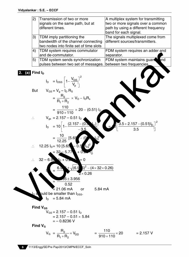
Comparison between TDM and FDM
TDM FDM 1) Total available time is divided
into several user Total frequency bands are divided into several users
1. (f)
fs
input
Ve(t) Low pass Filter (LPF)
Ve(t) Amplifier
A
f0 Voltage controlled oscillator (VCO) Vd(t)
Phase Detector Vin = Vinsint
Vidyala
nkar
Vidyalankar : S.E. – ECCF
1113/Engg/SE/Pre Pap/2013/CMPN/ECCF_Soln 6
2) Transmission of two or more signals on the same path, but at different times.
A multiplex system for transmitting two or more signals over a common path by using a different frequency band for each signal.
3) TDM imply partitioning the bandwidth of the channel connecting two nodes into finite set of time slots
The signals multiplexed come from different sources/transmitters.
4) TDM system requires commutator and de-commutator.
FDM system requires an adder and separator.
5) TDM system sends synchronization pulses between two set of messages.
FDM system maintains guard band between two frequencies.
Find ID
ID = IDSS 2
GS
p
V1
V
But VGS = Vg – ID RS
= 2
1 2
RR R
VD IDRs
= 110
910 110 20 (0.51) ID
Vgs = 2.157 – 0.51 ID
ID = 102
D(2.157 (0.51)I )1
3.5
= 102
D3.5 2.157 (0.51)I3.5
= 10
12.25 [5.657 (0.51) ID]2
12.25 ID = 10 [5.657 – 0.51 ID]2
= 32 – 5.77 ID + 0.26 2DI
32 – 6.995 ID + 0.26 2DI = 0
ID = 26.995 (6.995) (4 32 0.26)
2 0.26
= 6.995 3.956
0.52
= 21.06 mA or 5.84 mA ID should be smaller than IDSS. ID = 5.84 mA Find VGS VGS = 2.157 – 0.51 ID = 2.157 – 0.51 5.84 = – 0.8236 V Find VG
VG = 2DD
1 2
RV
R R
=
11020
910 110
= 2.157 V
2. (a)
Vidyala
nkar
Prelim Question Paper Solution
1113/Engg/SE/Pre Pap/2013/CMPN/ECCF_Soln 7
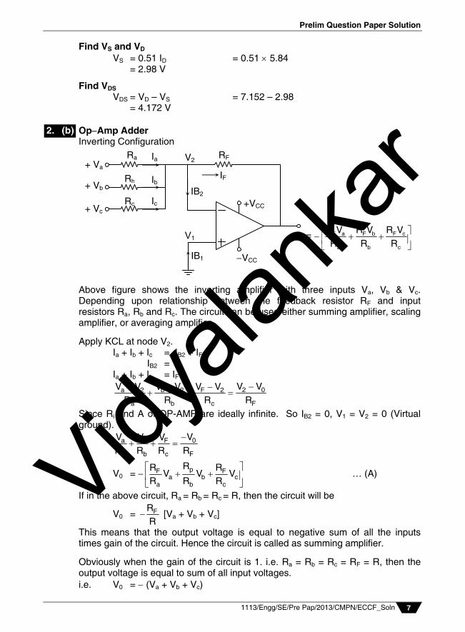
Find VS and VD VS = 0.51 ID = 0.51 5.84 = 2.98 V
Find VDS VDS = VD – VS = 7.152 – 2.98 = 4.172 V OpAmp Adder Inverting Configuration
Above figure shows the inverting amplifier with three inputs Va, Vb & Vc. Depending upon relationship between the feedback resistor RF and input resistors Ra, Rb and Rc. The circuit can be used either summing amplifier, scaling amplifier, or averaging amplifier.
Apply KCL at node V2. Ia + Ib + Ic = IB2 + IF IB2 = 0 Ia + Ib + Ic = IF
2 0a 2 b 2 F 2
a b c F
V VV V V V V VR R R R
Since Ri and A of OP-AMP are ideally infinite. So IB2 = 0, V1 = V2 = 0 (Virtual ground).
0a b F
a b c F
VV V VR R R R
V0 = pF Fa b c
a b c
RR RV V V
R R R
… (A)
If in the above circuit, Ra = Rb = Rc = R, then the circuit will be
V0 = FRR
[Va + Vb + Vc]
This means that the output voltage is equal to negative sum of all the inputs times gain of the circuit. Hence the circuit is called as summing amplifier.
Obviously when the gain of the circuit is 1. i.e. Ra = Rb = Rc = RF = R, then the output voltage is equal to sum of all input voltages. i.e. V0 = (Va + Vb + Vc)
2. (b)
V0 = F a F b F c
a b c
R V R V R VR R R
+VCC
VCC
Ib
Ic
Rb
Ra
Rc
+ Va
+ Vb
+ Vc
V2
V1
IB1
IB2
IF
RF Ia
Vidyala
nkar
Vidyalankar : S.E. – ECCF
1113/Engg/SE/Pre Pap/2013/CMPN/ECCF_Soln 8
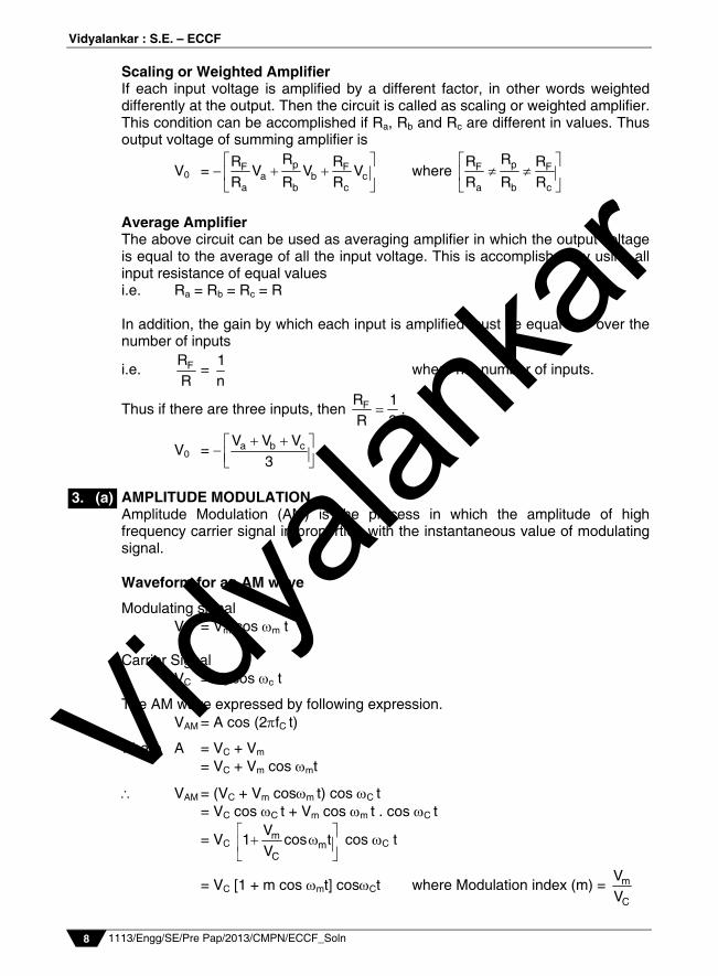
Scaling or Weighted Amplifier If each input voltage is amplified by a different factor, in other words weighted differently at the output. Then the circuit is called as scaling or weighted amplifier. This condition can be accomplished if Ra, Rb and Rc are different in values. Thus output voltage of summing amplifier is
V0 = pF Fa b c
a b c
RR RV V V
R R R
where pF F
a b c
RR RR R R
Average Amplifier The above circuit can be used as averaging amplifier in which the output voltage is equal to the average of all the input voltage. This is accomplished by using all input resistance of equal values i.e. Ra = Rb = Rc = R In addition, the gain by which each input is amplified must be equal to 1 over the number of inputs
i.e. FRR
= 1n
where n = number of inputs.
Thus if there are three inputs, then FR 1R 3
.
V0 = a b cV V V3
AMPLITUDE MODULATION Amplitude Modulation (AM) is the process in which the amplitude of high frequency carrier signal in proportion with the instantaneous value of modulating signal. Waveform for an AM wave
Modulating signal Vm = Vm cos m t Carrier Signal VC = Vc cos c t
The AM wave expressed by following expression. VAM = A cos (2fC t)
where A = VC + Vm = VC + Vm cos mt
VAM = (VC + Vm cosm t) cos C t = VC cos C t + Vm cos m t . cos C t
= VC mm
C
V1 cos t
V
cos C t
= VC [1 + m cos mt] cosCt where Modulation index (m) = m
C
VV
3. (a)
Vidyala
nkar
Prelim Question Paper Solution
1113/Engg/SE/Pre Pap/2013/CMPN/ECCF_Soln 9
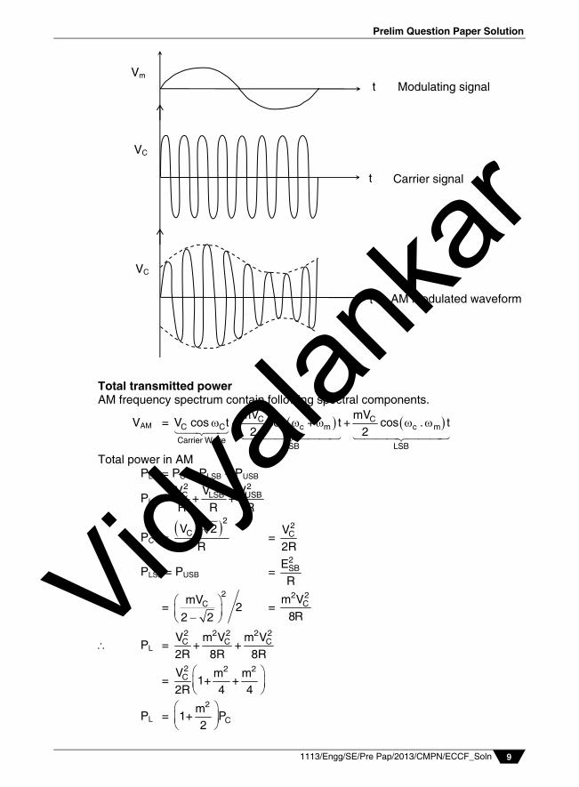
Total transmitted power AM frequency spectrum contain following spectral components.
VAM = C CC C c m c m
Carrier WaveUSB LSB
mV mVV cos t + cos + t + cos . t
2 2
Total power in AM PL = PC + PLSB + PUSB
PL = 2 2 2C LSB USBV V V
+ +R R R
PC = 2CV / 2
R =
2CV
2R
PLSB = PUSB = 2SBER
= 2
CmV2
2 2
= 2 2
Cm V8R
PL = 2 2 2 2 2C C CV m V m V
+ +2R 8R 8R
= 2 2 2CV m m
1+ +2R 4 4
PL = 2
Cm
1+ P2
t
t
t
VC
VC
Vm
Modulating signal
Carrier signal
AM modulated waveform
Vidyala
nkar
Vidyalankar : S.E. – ECCF
1113/Engg/SE/Pre Pap/2013/CMPN/ECCF_Soln 10
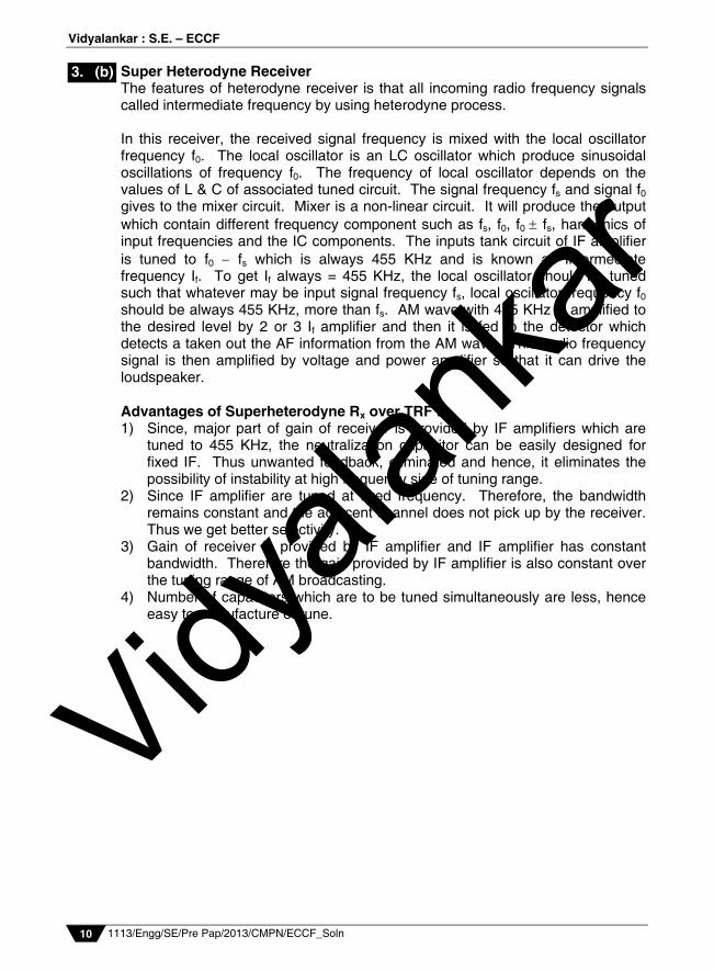
Super Heterodyne Receiver The features of heterodyne receiver is that all incoming radio frequency signals called intermediate frequency by using heterodyne process. In this receiver, the received signal frequency is mixed with the local oscillator frequency f0. The local oscillator is an LC oscillator which produce sinusoidal oscillations of frequency f0. The frequency of local oscillator depends on the values of L & C of associated tuned circuit. The signal frequency fs and signal f0 gives to the mixer circuit. Mixer is a non-linear circuit. It will produce the output which contain different frequency component such as fs, f0, f0 fs, harmonics of input frequencies and the IC components. The inputs tank circuit of IF amplifier is tuned to f0 fs which is always 455 KHz and is known as Intermediate frequency If. To get If always = 455 KHz, the local oscillator should be tuned such that whatever may be input signal frequency fs, local oscillator frequency f0 should be always 455 KHz, more than fs. AM wave with 455 KHz is amplified to the desired level by 2 or 3 If amplifier and then it is fed to the detector which detects a taken out the AF information from the AM wave. This audio frequency signal is then amplified by voltage and power amplifier so that it can drive the loudspeaker. Advantages of Superheterodyne Rx over TRF Rx 1) Since, major part of gain of receiver is provided by IF amplifiers which are
tuned to 455 KHz, the neutralization capacitor can be easily designed for fixed IF. Thus unwanted feedback, eliminated and hence, it eliminates the possibility of instability at high frequency side of tuning range.
2) Since IF amplifier are tuned at fixed frequency. Therefore, the bandwidth remains constant and the adjacent channel does not pick up by the receiver. Thus we get better selectivity.
3) Gain of receiver is provided by IF amplifier and IF amplifier has constant bandwidth. Therefore the gain provided by IF amplifier is also constant over the tuning range of AM broadcasting.
4) Number of capacitors which are to be tuned simultaneously are less, hence easy to manufacture or tune.
3. (b)
Vidyala
nkar
Prelim Question Paper Solution
1113/Engg/SE/Pre Pap/2013/CMPN/ECCF_Soln 11
Block diagram of Superheterodyne Receiver
Vidyala
nkar
Vidyalankar : S.E. – ECCF
1113/Engg/SE/Pre Pap/2013/CMPN/ECCF_Soln 12
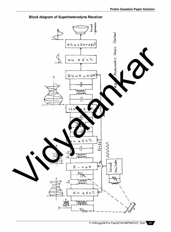
Characteristics of Receiver 1) Sensitivity It is the ability of the receiver to
receive weak signal and it is defined as the amount of input voltage required for the receiver to produce standard output power (50 mV) at its output.
Sensitivity is expressed in V or dB below 1V. The typical sensitivity curve is as shown :
From the curve it is seen that radio receiver is most sensitive at 850 KHz as the frequency increases, the gain of receiver decreases. Therefore more input voltage required to produce standard output. Therefore at high frequency, the sensitivity of receiver is less. The sensitivity of receiver depends on the gain of RF and IF amplifier.
Sensitivity Measurement While measuring sensitivity, the receiver source and load must be
standardised so that variation is the measurement and do not affect the output. For this purpose actual antenna is replaced by dummy antenna which is LC tuned circuit and the load is not loudspeaker but its resistor.
A standard input AM signal at 30% modulation and FM = 400 Hz is applied to
receiver through the dummy antenna. The input is varied by using voltage control to get standard output power of 50 mV across the load. The input in V of carrier voltage is a measure of sensitivity.
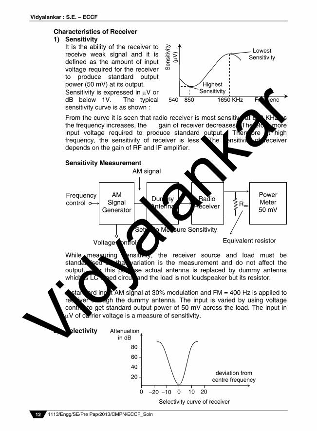
2) Selectivity
540 850 1650 KHz
Lowest Sensitivity
Highest Sensitivity
Frequenc
Sen
sitiv
ity
(V
) AM signal
Frequency control
AM Signal
Generator
Dummy Antenna
Radio Receiver
Power Meter 50 mV
Setup to Measure Sensitivity
Voltage control Equivalent resistor
Req
0
deviation from centre frequency
Attenuation in dB
20 10 0 10 20
Selectivity curve of receiver
20
40
60
80 Vidyala
nkar
Prelim Question Paper Solution
1113/Engg/SE/Pre Pap/2013/CMPN/ECCF_Soln 13
Selectivity of receiver is defined as the ability of the receiver to select desired signal or channel and reject unwanted signal or adjacent channel. The selectivity curve of receiver is as shown above. When the receiver receives the frequency signal at which receiver is tuned (centre frequency). It will provide maximum gain/zero attenuation but as the input signal frequency deviates from the centre frequency the gain of receiver decreases i.e. attenuation increases.
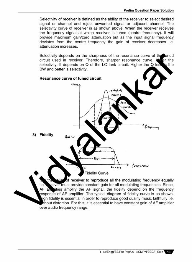
Selectivity depends on the sharpness of the resonance curve of the tuned
circuit used in receiver. Therefore, sharper resonance curve, better the selectivity. It depends on Q of the LC tank circuit. Higher the Q less is the BW and better is selectivity.
Resonance curve of tuned circuit 3) Fidelity It is the ability of receiver to reproduce all the modulating frequency equally
i.e. receiver must provide constant gain for all modulating frequencies. Since, AF amplifies amplify the AF signal, the fidelity depend on the frequency response of AF amplifier. The typical diagram of fidelity curve is as shown. High fidelity is essential in order to reproduce good quality music faithfully i.e. without distortion. For this, it is essential to have constant gain of AF amplifier over audio frequency range.
Fidelity Curve
Vidyala
nkar
Vidyalankar : S.E. – ECCF
1113/Engg/SE/Pre Pap/2013/CMPN/ECCF_Soln 14
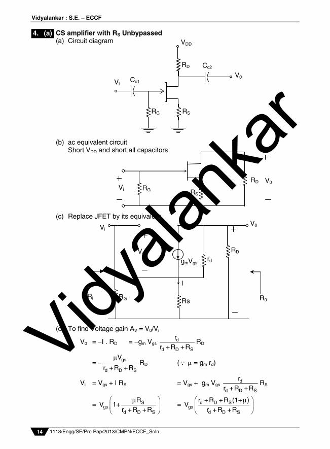
CS amplifier with RS Unbypassed (a) Circuit diagram (b) ac equivalent circuit Short VDD and short all capacitors
(c) Replace JFET by its equivalent
(d) To find Voltage gain AV = V0/Vi
V0 = I . RD = gm Vgs d
d D S
rr +R +R
RD
= gs
d D S
V
r +R +R
RD ( = gm rd)
Vi = Vgs + I RS = Vgs + gm Vgs d
d D S
rr +R +R
RS
= Sgs
d D S
RV 1+
r +R +R
= d D Sgs
d D S
r +R +R (1+ )V
r +R +R
4. (a)
Vi
RD
RG
V0
RS
Vgs gmVgs
RD
RG
Vi
Ri R0
V0
rd
Rs
I
Vi Cc1
Cc2 RD
VDD
V0
RG RS
Vidyala
nkar
Prelim Question Paper Solution
1113/Engg/SE/Pre Pap/2013/CMPN/ECCF_Soln 15
Av = D
d D S
Rr +R +R (1+ )
(e) To find Input impedance Ri Ri = RG (f) To Find Output impedance R0 R0 = [rd + RS (1 + )] || RD
Results (with rd) Results (without rd)
Av = D
d D S
Rr +R +R (1+ )
where = gm rd Ri = RG
R0 = [rd + RS (1 + )] || RD
Av = m D
m S
g R1+ g R
Ri = RG
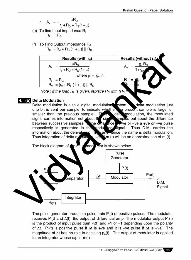
R0 = RD
Note : If the load RL is given, replace RD with (RD || RL) Delta Modulation Delta modulation is also a digital modulation system. In delta modulation just one bit is sent per sample, to indicate whether the present sample is larger or smaller than the previous sample. Thus in delta modulation, the modulated signal carries information not about the signal samples but about the difference between successive samples. If the difference is +ve or ve a +ve or ve pulse respectively is generated in the modulated signal. Thus D.M. carries the information about the derivative of m (t) and hence the name is delta modulation. Thus integration of delta modulated signal m (t) will be an approximation of m (t). The block diagram of the delta modulator is shown below. The pulse generator produce a pulse train Pi(t) of positive pulses. The modulator receives Pi(t) and (t), the output of differential amp. The modulator output Po(t) is the product of input pulse train Pi(t) and +1 or 1 depending upon the polarity of t. Po(t) is positive pulse if t is +ve and it is ve pulse if t is ve. The magnitude of t has no role in deciding po(t). The output of modulator is applied to an integrator whose o/p is m(t) .
4. (b)
Pulse Generator
Modulator
Comparator
Integrator
D.M. Signal
Po(t) t
(t)m
Pi(t) m(t)
Vidyala
nkar
Vidyalankar : S.E. – ECCF
1113/Engg/SE/Pre Pap/2013/CMPN/ECCF_Soln 16
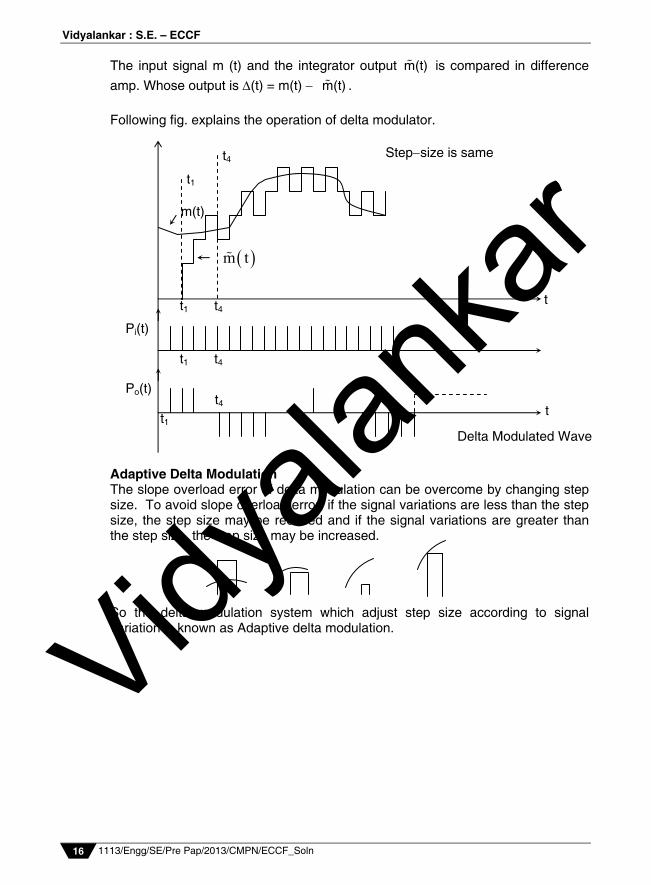
The input signal m (t) and the integrator output m(t) is compared in difference
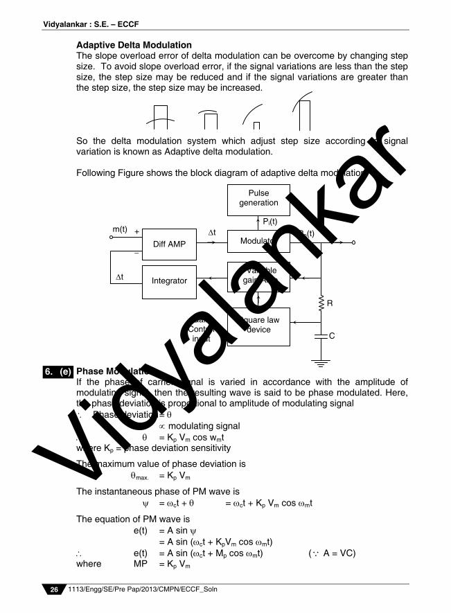
amp. Whose output is (t) = m(t) m(t) . Following fig. explains the operation of delta modulator. Adaptive Delta Modulation The slope overload error of delta modulation can be overcome by changing step size. To avoid slope overload error, if the signal variations are less than the step size, the step size may be reduced and if the signal variations are greater than the step size, the step size may be increased. So the delta modulation system which adjust step size according to signal variation is known as Adaptive delta modulation.
Delta Modulated Wave
t
Po(t)
t1 t4
Pi(t)
t
t1
t4
m t
m(t)
Stepsize is same
t1 t4
t1 t4
Vidyala
nkar
Prelim Question Paper Solution
1113/Engg/SE/Pre Pap/2013/CMPN/ECCF_Soln 17
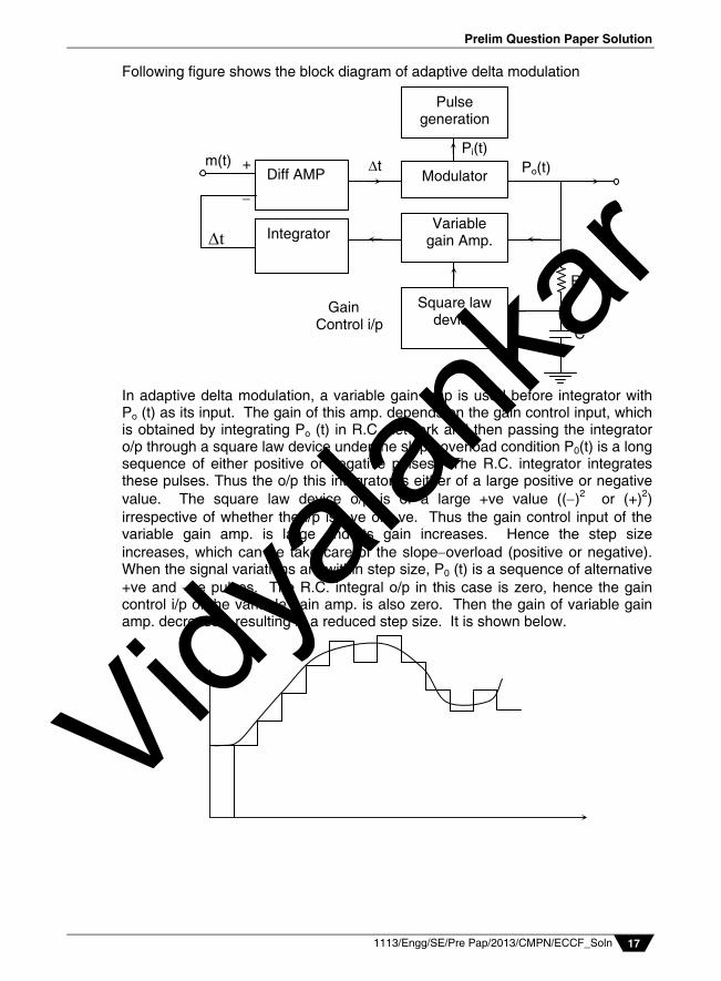
Following figure shows the block diagram of adaptive delta modulation In adaptive delta modulation, a variable gain amp is used before integrator with Po (t) as its input. The gain of this amp. depends on the gain control input, which is obtained by integrating Po (t) in R.C. network and then passing the integrator o/p through a square law device under the slope overload condition P0(t) is a long sequence of either positive or negative pulses. The R.C. integrator integrates these pulses. Thus the o/p this integrator is either of a large positive or negative value. The square law device o/p is of a large +ve value (()2 or (+)2) irrespective of whether the i/p is +ve or ve. Thus the gain control input of the variable gain amp. is large and its gain increases. Hence the step size increases, which can be take care of the slopeoverload (positive or negative). When the signal variations are within step size, P0 (t) is a sequence of alternative +ve and ve pulses. The R.C. integral o/p in this case is zero, hence the gain control i/p of the variable gain amp. is also zero. Then the gain of variable gain amp. decreases, resulting in a reduced step size. It is shown below.
Pulse generation
Modulator
Square law device
Diff AMP
Integrator
+
C
m(t)
Gain Control i/p
Po(t)
R
Variable gain Amp.
Pi(t) t
t
Vidyala
nkar
Vidyalankar : S.E. – ECCF
1113/Engg/SE/Pre Pap/2013/CMPN/ECCF_Soln 18
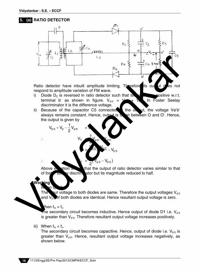
RATIO DETECTOR Ratio detector have inbuilt amplitude limiting. Therefore its output does not respond to amplitude variation of FM wave. i) Diode D2 is reversed in ratio detector such that terminal O is positive w.r.t.
terminal b as shown in figure. Vab = Va0 + Vb0. In Foster Seelay discriminator it is the difference voltage.
ii) Because of the capacitor C5 connected at the output, the voltage Vab always remains constant. Hence, output is taken between O and O. Hence, the output is given by
b 0 0 a b1
V V V2 = 0
V0 = a b b 01
V V2
= a 0 b 0b 0
V VV
2
V0 = a 0 b 01
V V2
Above equation shows that the output of ratio detector varies similar to that of foster seeley discriminator but its magnitude reduced to half.
Working : i) When fin = fc. The input voltage to both diodes are same. Therefore the output voltages Va0
and Vb0 of both diodes are identical. Hence resultant output voltage is zero. ii) When fin > fc. The secondary circuit becomes inductive. Hence output of diode D1 i.e. Va0
is greater than Vb0. Therefore resultant output voltage increases positively. iii) When fin < fc. The secondary circuit becomes capacitive. Hence, output of diode i.e. Vb0 is
greater than Va0. Hence, resultant output voltage increases negatively, as shown below.
5. (a)
Vidyala
nkar
Prelim Question Paper Solution
1113/Engg/SE/Pre Pap/2013/CMPN/ECCF_Soln 19
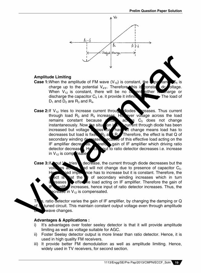
Amplitude Limiting Case 1: When the amplitude of FM wave (V12) is constant, the capacitance C5 is
charge up to the potential Vab. Therefore, this is constant dc voltage. When V12 is constant, there will be no current either to charge or discharge the capacitor C5 i.e. it provide it infinite impedance. The load of D1 and D2 are R3 and R4.
Case 2: If V12 tries to increase current through diodes increases. Thus current
through load R3 and R4 increases. However voltage across the load remains constant because voltage across C5 does not change instantaneously. Now the situation is that current through diode has been increased but voltage across load has not change means load has to decreases but load is fixed (R3 and R4). Therefore, the effect is that Q of secondary winding decreases because of this effective load acting on the IF amplifier decreases. Therefore gain of IF amplifier which driving ratio detector decreases. Hence input to ratio detector decreases i.e. increase in V12 is compensated.
Case 3: If input V12 tries to decrease, the current through diode decreases but the
voltages across load will not change due to presence of capacitor C5. Hence, load impedance has to increase but it is constant. Therefore, the effect is that the Q of secondary winding increases which in turn increases the effective load acting on IF amplifier. Therefore the gain of IF amplifier increases, hence input of ratio detector increases. Thus, the decrease in V12 is compensated.
Thus, ratio detector varies the gain of IF amplifier, by changing the damping or Q of its tuned circuit. This maintain constant output voltage even through amplitude of FM wave changes. Advantages & Applications : i) It’s advantages over foster seeley detector is that it will provide amplitude
limiting as well as voltage suitable for AGC. ii) Foster Seelay detector output is more linear than ratio detector. Hence, it is
used in high quality FM receivers. iii) It provide better FM demodulation as well as amplitude limiting. Hence,
widely used in TV receivers, for second section.
Vidyala
nkar
Vidyalankar : S.E. – ECCF
1113/Engg/SE/Pre Pap/2013/CMPN/ECCF_Soln 20
SAMPLING THEOREM Types of sampling Impulse sampling s(t) Impulse train Natural sampling Flat top sampling FDR of Impulse sampling Fourier expansion of s(t) :
s(t) = 0 n n n nn=1 n=1
A + A cos t + B sin t
where A0 = s
S
T /2
S T /2
1s(t).dt
T
An = s
S
T /2
sS T /2
2s(t).cos n t.dt
T
Bn = s
S
T /2
sS T /2
2s(t).sin n t.dt
T
We calculate Fourier series for the above mentioned sample :
A0 = dt/2
S dt/2
11.dt
T
A0 = dt/2dt/2
S
1[dt]
T
A0 = S
1 dt dt+
T 2 2
Hence A0 = S
dtT
An = dt/2
ss dt/2
21.cos n t.dt
T
An = dt/2
s
S s dt/2
sinn t2T n
An = s s
s s
sinn dt sinn dt2nT 2 2
An = s
s s
2sinn dt/22dt.
2T n dt/2
5. (b)
s(t) Pulse train
s(t)
1
dt
Vidyala
nkar
Prelim Question Paper Solution
1113/Engg/SE/Pre Pap/2013/CMPN/ECCF_Soln 21
An = s
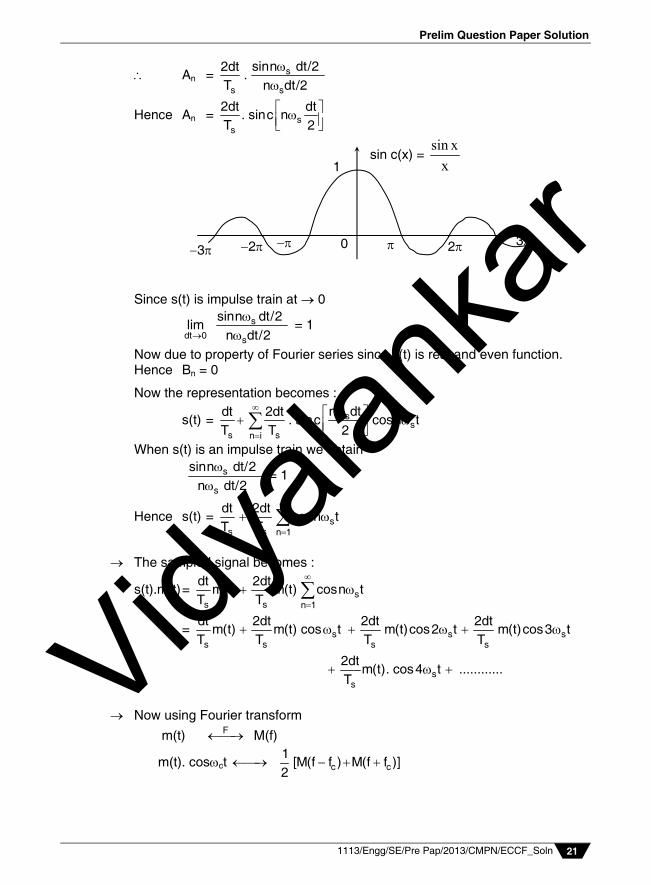
s s
sinn dt/22dt.
T n dt/2
Hence An = ss
2dt dt. sinc n
T 2
Since s(t) is impulse train at 0
s
dt 0 s
sinn dt/2lim
n dt/2
= 1
Now due to property of Fourier series since s(t) is real and even function. Hence Bn = 0
Now the representation becomes :
s(t) = ss
s sn i
n dtdt 2dt. sinc cosn t
T T 2
When s(t) is an impulse train we obtain
s
s
sinn dt/2n dt/2
= 1
Hence s(t) = ss s n 1
dt 2dtcosn t
T T
The sampled signal becomes :
s(t).m(t) = ss s n 1
dt 2dtm(t) m(t) cosn t
T T
= s s ss s s s
dt 2dt 2dt 2dtm(t) m(t) cos t m(t)cos2 t m(t)cos3 t
T T T T
ss
2dtm(t). cos4 t ............
T
Now using Fourier transform
m(t) F M(f)
m(t). cosct c c1
[M(f f ) M(f f )]2
sin c(x) = sin xx
1
3 2 0 2 3
Vidyala
nkar
Vidyalankar : S.E. – ECCF
1113/Engg/SE/Pre Pap/2013/CMPN/ECCF_Soln 22
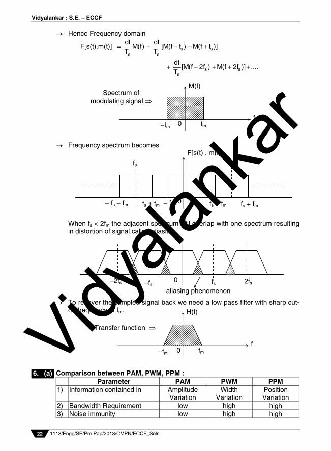
Hence Frequency domain
F[s(t).m(t)] = s ss s
dt dtM(f) [M(f f ) M(f f )]
T T
s ss
dt[M(f 2f ) M(f 2f )] ....
T
Frequency spectrum becomes When fs < 2fm the adjacent spectrum will overlap with one spectrum resulting
in distortion of signal called aliasing. To recover the sampled signal back we need a low pass filter with sharp cut-
off frequency of fm. Comparison between PAM, PWM, PPM :
Parameter PAM PWM PPM 1) Information contained in Amplitude
Variation Width
Variation Position Variation
2) Bandwidth Requirement low high high 3) Noise immunity low high high
6. (a)
fs fs F[s(t) . m(t)]
fs fm fs + fm fm 0 fm fs fm fs + fm
0 2fs 2fs fs fs aliasing phenomenon
H(f)
f fm fm
Transfer function
0
M(f)
f fm fm
Spectrum of modulating signal
0
Vidyala
nkar
Prelim Question Paper Solution
1113/Engg/SE/Pre Pap/2013/CMPN/ECCF_Soln 23
4) Transmitted Power Varies with amplitude &
pulses
Varies with variation in
width
Remains constant
5) Need to transmitt synchronization pulses
not needed not needed necessary
6) Complexity of generation & detection
Complex Easy Complex
An ideal opamp exhibits the following electrical characteristics. (a) Infinite voltage gain (b) Infinite input resistance Ri, so that any signal source can drive it and there is
no loading of the preceding stage. (c) Zero output resistance R0, so that output can drive an infinite number of other
devices. (d) Zero offset voltage, hence can be direct coupled. (e) Infinite BW, so that frequencies from 0 to Hz can be amplified without
attenuation. (f) Infinite CMRR, so that common mode noise is zero. (g) Infinite slew rate, so that output voltage changes simultaneously with input. Zero Crossing Detectors Zero crossing detector is nothing but the basic comparator circuit with a zero reference voltage applied to the non-inverting terminal. Circuit Operation : Refer to waveforms, when the input sinewave crosses zero and becomes +ve at instant t = 0, the differential input voltage Vd becomes negative and output voltage will swing to –V(sat). When the sinewave again crosses zero and becomes negative at instant t = T/2, the differential input voltage becomes +ve and output voltage will swing to +V(sat) as now the (+) terminal is more +ve than the (–) terminal. The zero crossing detector thus switches its output from one state to other every time when the input voltage crosses zero.
The ZCD is also known as sinewave to square wave converter.
6. (b)
6. (c)
+VCC
–VCC
Vd
Vin
R
Vref = 0
Vo
Vin
t 0
+Vsat
t 0
Vo
T
–Vsat
Input and Output voltage waveforms
Vidyala
nkar
Vidyalankar : S.E. – ECCF
1113/Engg/SE/Pre Pap/2013/CMPN/ECCF_Soln 24
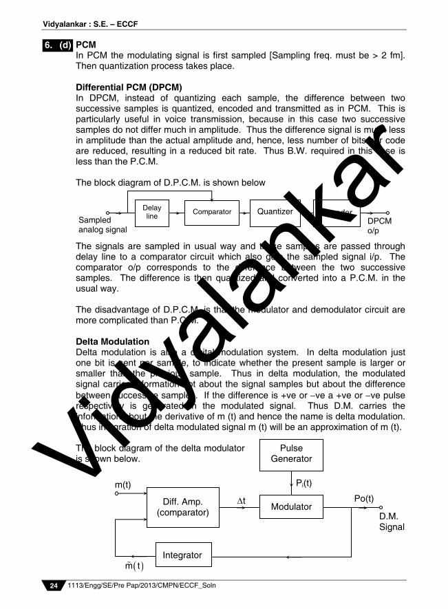
PCM In PCM the modulating signal is first sampled [Sampling freq. must be > 2 fm]. Then quantization process takes place. Differential PCM (DPCM) In DPCM, instead of quantizing each sample, the difference between two successive samples is quantized, encoded and transmitted as in PCM. This is particularly useful in voice transmission, because in this case two successive samples do not differ much in amplitude. Thus the difference signal is much less in amplitude than the actual amplitude and, hence, less number of bits per code are reduced, resulting in a reduced bit rate. Thus B.W. required in this case is less than the P.C.M. The block diagram of D.P.C.M. is shown below The signals are sampled in usual way and these samples are passed through delay line to a comparator circuit which also gets the sampled signal i/p. The comparator o/p corresponds to the difference between the two successive samples. The difference is then quantized and converted into a P.C.M. in the usual way. The disadvantage of D.P.C.M. is that the modulator and demodulator circuit are more complicated than P.C.M. Delta Modulation Delta modulation is also a digital modulation system. In delta modulation just one bit is sent per sample, to indicate whether the present sample is larger or smaller than the previous sample. Thus in delta modulation, the modulated signal carries information not about the signal samples but about the difference between successive samples. If the difference is +ve or ve a +ve or ve pulse respectively is generated in the modulated signal. Thus D.M. carries the information about the derivative of m (t) and hence the name is delta modulation. Thus integration of delta modulated signal m (t) will be an approximation of m (t). The block diagram of the delta modulator is shown below.
6. (d)
Pulse Generator
Modulator
Diff. Amp. (comparator)
Integrator
D.M. Signal
Po(t) t
m t
Pi(t) m(t)
Delay line
Comparator
Quantizer
Encoder Sampled analog signal
DPCM o/p
Vidyala
nkar
Prelim Question Paper Solution
1113/Engg/SE/Pre Pap/2013/CMPN/ECCF_Soln 25
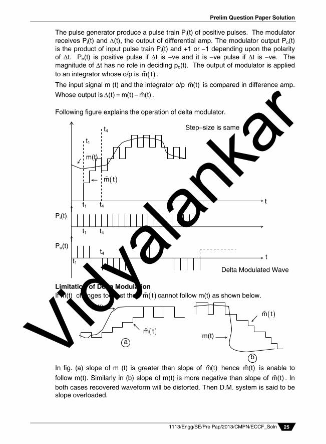
The pulse generator produce a pulse train Pi(t) of positive pulses. The modulator receives Pi(t) and (t), the output of differential amp. The modulator output Po(t) is the product of input pulse train Pi(t) and +1 or 1 depending upon the polarity of t. Po(t) is positive pulse if t is +ve and it is ve pulse if t is ve. The magnitude of t has no role in deciding po(t). The output of modulator is applied to an integrator whose o/p is m t .
The input signal m (t) and the integrator o/p m(t) is compared in difference amp.
Whose output is (t) m(t) m(t) . Following figure explains the operation of delta modulator.
Limitation of Delta Modulation If m(t) changes too fast then m t cannot follow m(t) as shown below.
In fig. (a) slope of m (t) is greater than slope of m(t) hence m(t) is enable to
follow m(t). Similarly in (b) slope of m(t) is more negative than slope of m(t) . In both cases recovered waveform will be distorted. Then D.M. system is said to be slope overloaded.
m(t)
m t
a
b
m(t)
m t
Delta Modulated Wave
t
Po(t)
t1 t4
Pi(t)
t
t1
t4
m t
m(t)
Stepsize is same
t1 t4
t1 t4
Vidyala
nkar
Vidyalankar : S.E. – ECCF
1113/Engg/SE/Pre Pap/2013/CMPN/ECCF_Soln 26
Adaptive Delta Modulation The slope overload error of delta modulation can be overcome by changing step size. To avoid slope overload error, if the signal variations are less than the step size, the step size may be reduced and if the signal variations are greater than the step size, the step size may be increased. So the delta modulation system which adjust step size according to signal variation is known as Adaptive delta modulation. Following Figure shows the block diagram of adaptive delta modulation
Phase Modulation If the phase of carrier signal is varied in accordance with the amplitude of modulating signal, then the resulting wave is said to be phase modulated. Here, the phase deviation is proportional to amplitude of modulating signal Phase deviation = modulating signal = Kp Vm cos wmt where Kp = phase deviation sensitivity
The maximum value of phase deviation is max. = Kp Vm
The instantaneous phase of PM wave is = ct + = ct + Kp Vm cos mt
The equation of PM wave is e(t) = A sin = A sin (ct + KpVm cos mt) e(t) = A sin (ct + Mp cos mt) ( A = VC) where MP = Kp Vm
6. (e)
Pulse generation
Modulator
Square law device
Diff AMP
Integrator
+
C
m(t)
Gain Control input
Po(t)
R
Variable gain Amp.
Pi(t) t
t
Vidyala
nkar
Prelim Question Paper Solution
1113/Engg/SE/Pre Pap/2013/CMPN/ECCF_Soln 27
MP is modulation index of phase modulation and it is proportional to amplitude of modulating signal and it is independent of frequency of modulating signal. Bandwidth of PM : The instantaneous phase of PM is = ct + Kp cos mt
the instantaneous frequency is
Wi = ddt
= c p m md
[ t k v cos t]dt
= c p m m mK V sin t
Wi = c
So maximum value of frequency deviation is PM is max. = Kp Vm m
Frequency deviation in PM is to amplitude as well as frequency of modulating signal as per Carson rule bandwidth require for PM is BW = 2( + fm)
Vidyala
nkar

![S.E. Sem. III [CMPN] Digital Logic Design and Analysis ...vidyalankar.org/.../prelim_paper_soln/SemIII/CMPN/DLDA_Soln.pdf · 1113/Engg/SE/Pre Pap/2013/CMPN/DLDA_Soln1 Vidyalankar](https://img.pdfslide.us/doc/110x75/5aca396c7f8b9a51678dc11a/se-sem-iii-cmpn-digital-logic-design-and-analysis-pap2013cmpndldasoln1.jpg)


![T.E. Sem. V [CMPN] Advanced Database Management …vidyalankar.org/file/engg_degree/prelim_paper_soln/SemV/CMPN/ADBMS.pdfAdvanced Database Management Systems Prelim Question Paper](https://img.pdfslide.us/doc/110x75/5ad9973d7f8b9a86378c2f07/te-sem-v-cmpn-advanced-database-management-database-management-systems.jpg)


![B.E. Sem. VII [EXTC] Fundamentals of Microwave …vidyalankar.org/file/engg_degree/prelim_paper_soln/SemVII/EXTC/... · Fundamentals of Microwave Engineering Prelim Question Paper](https://img.pdfslide.us/doc/110x75/5ab168727f8b9ad9788c3916/be-sem-vii-extc-fundamentals-of-microwave-of-microwave-engineering-prelim.jpg)


![B.E. Sem. VII [INFT] Vidyalankarvidyalankar.org/file/engg_degree/prelim_paper_soln/SemVII/INFT/DWM.… · Therefore it flows into a Decision Support System (DSS) or into marketing](https://img.pdfslide.us/doc/110x75/5a9db36e7f8b9a85318b9f3f/be-sem-vii-inft-vi-therefore-it-flows-into-a-decision-support-system-dss.jpg)