Embed Size (px)
Citation preview
VGF GaP - LED's IST-2001-32793 Final Public Report
D
D
raft 5th February 2006
Final Public Report of VGF GaP - LED's Activity
Project start date: 1 March 2002 Project duration: 42 months
Project Co-ordinator Organisation: CiS Institute for Microsensors (non-profit) Ltd.
Responsible person: Dietmar Starke Phone: +49 361 663 1474
Fax: +49 361 663 1423 Email: [email protected]
Consortium Composition
1 CiS Institute for Microsensors (non-profit) Ltd. Erfurt, Germany 2 PHOSTEC s.r.o. Žarnovica, Slovakia 3 Slovak Academy of Sciences, Institute of Electrical Engineering 4 Slovak University of Technology, Department of Microelectronics
OCUMENT HISTORY
Release Date Reason of change Status Distribution 1.0 31.08.2005 Candidate public release draft Project team, reviewers 1.1 19.09.2005 Final public release draft Project team, reviewers 1.2 19.10.2005 Final public release draft Project team, reviewers 1.3 05.02.2006 Final public release draft Project team 1.4 07.02.2006 Final public release final Project team, reviewers
VGF GaP - LED's
Project IST - 2001 - 32793 New gallium phosphide grown by vertical gradient freeze method for light emitting diodes
Project funded by the European Community under the "InformationSociety Technologies" Programme
(1998 -2002)
Page 1 of 30
VGF GaP - LED's IST-2001-32793 Final Public Report
Draft 5th February 2006 Page 2 of 30
Table of contents Preamble 1 Executive Summary 2 Project objectives 2.1 Motivation 2.2 How does VGF work ? 3 Methodologies 3.1 State-of-the art 3.2 Principle of approaches 4 Project results 4.1 Target focussing 4.2 Achievements 4.3 Raising awareness 4.4 Impact with technical prospect 5 Outcomes 5.1 Improved indium phosphide growth 5.2 Pyrolytic coatings 5.3 Specification of the VGF GaP procedure and furnace 5.4 New VGF GaP substrate 5.5 Experiences in homo and heterostructures for LED device design 5.6 Directly grown GaP LEDs 5.7 New experiences with the MOVPE procedure 6 Exploitation strategy
7 Co-operation outlook and work forwards 8 Lessons learnt and conclusions References

VGF GaP - LED's IST-2001-32793 Final Public Report
Draft 5th February 2006 Page 3 of 30
Preamble In this document, the abbreviation "CiS" is used for CiS Institut fuer Mikrosensorik (non-profit) GmbH (Germany), "PHOSTEC" is used for PHOSTEC s.r.o. (Slovakia), "SAS" is used for Institute for Electrical Engineering as part of the Slovak Academy of Sciences (Slovakia), and "FEI STU" is used for Slovak University of Technology, Department of Microelectronics (Slovakia). 1 Executive Summary This document is the final project report for the VGF GaP - LED's project (1), which has found an approach to synthesis and crystal growth of gallium phosphide (GaP) by vertical gradient freeze method (VGF), that makes it possible to produce GaP single crystal substrates for LEDs with small quantity of structural defects. That's means to elaborate and define those combination set of parameters describing the VGF process for GaP single crystal growth leading to a low level of structural defect. Recently, the LEC standard technology (Liquid Encapsulated Czochralski) provides GaP material in the range of 30.000-200.000 defects/cm2 in the crystal lattice of semiconductor. Using the new procedure based on the VGF technology manufacturers of GaP substrate will be in the position to produce GaP single crystals with 100 - 1000 times lower number of structural defects. Such VGF defect-reduced GaP single crystals open the door for innovations in the fields of brightness and applications of light emitting diodes (LED). Consequently, it is evident that the VGF GaP - LED's project has been integrating a part of design and development of advanced LED structures, which can be used for evaluation of VGF GaP. Following the defined work plan, the project has elaborated both, a synthesis procedure and equipment for growing gallium phosphide single crystals with small quantum of structural defects by using VGF method and a new LED structure design. The primary motivation for the project has been fed by the fact that the importance of LED's for our day-to-day life is increasing and for this purpose, better and cheaper GaP substrate has to be available. GaP substrate is till now applicable for manufacturing of red, amber and green standard brightness LED's and further, red and yellow super high brightness LED's. The ultimate motivation is to prepare a route for producing of VGF GaP substrate in Europe because there is no such a production in the states of the European community. A summary description of the way to approach GaP single crystal with 100 - 1000 times lower number of structural defects is provided (section 3.2), including a sample and prototype for a newly designed LED structure. The approach to the use of the VGF methods for GaP single crystal growing with low structural defects has been opening by • a set of experimental steps and trials aimed to synthesis of GaP and InP (indium phosphide) as
related substitute material (section 5.1), • coating the VGF crucible and other needed graphite parts by specific pyrolytic layers (section 5.2), • elaborating a new specification for the VGF GaP procedure and crucible in connection with a
material-specific simulation of the temperature field (section 5.3), • development of a reproducible VGF GaP growing process for single crystals (section 5.4), • novel designing LED structures for better characteristics based on direct growth on GaP substrate
(section 5.5) and, • new experiences with MOVPE growth of GaP LED structures (section 5.6). Using the dissemination expertise and the industrial involvement of CiS as manufacturer of semiconductor-based sensors and post-stage LED user we have developed and executed a strategy for publicising/sharing our activities to/with the European LED community as well on scientific as business level, reaching the European LED device manufacturers from epi-ready substrate up to packaging. In order to ensure an industry-proof validation and test for the new GaP substrate the consortium has established a European user group for manufacturing "epi-ready" wafers and LED’s.

VGF GaP - LED's IST-2001-32793 Final Public Report
Draft 5th February 2006 Page 4 of 30
For a better business addressing the VGF GaP substrate in connection with directly grown LED structures to the post-stage LED users CiS has elaborated jointly with SAS and FEI STU an application support. To complete the set of VGF GaP process parameters for reaching a structural defect low level the project team has decided to continue the work to reach the full reproducibility of the VGF GaP process. For this purpose, CiS and PHOSTEC will get in a new joint bilateral project. The latest information about the VGF GaP - LED's project may be found at the project website under www.vgfgapleds.sk (2).
2 Project objectives The main goal, development of VGF gallium phosphide (GaP) substrate is divided into the following subtasks:
− Development of GaP single crystal with small quantity of structural defects grown by vertical gradient freeze method (VGF);
− Preparation of VGF GaP substrate, manufacturing, and industrial proof of the new VGF GaP substrate by direct users of GaP "epi-ready" wafers.
To validate the new VGF GaP wafers the consortium has established a specific industrial user group.
2.1 Motivation Almost all commercially available GaP wafers are produced now out of Europe from single crystals, which are grown by the method LEC (Liquid Encapsulated Czochralski). This is a traditional procedure of production A3B5 single crystals (GaP, GaAs, InP etc.), but for GaP this method has essential disadvantages: • diameter limitation to grow 3" GaP single crystals as today observed on the world market, • very high density of structural defects (so-called Etched Pit Density EPD) of single crystals due to
the high temperature gradient during the process of growth. One way how to solve the main challenge of EPD is to use the VGF single crystal growth (Vertical Gradient Freeze). In the VGF technology the crystals are grown under very low temperature gradient and it is confirmed, that typical EPD is lower than 1000 defects / cm2 and central part of the wafer is usually even dislocation free. The use of VGF method for GaP is complicated due to high phosphorus vapour pressure in the range of 40 - 70 bar and due to the high temperature of GaP melting point - 1457°C.
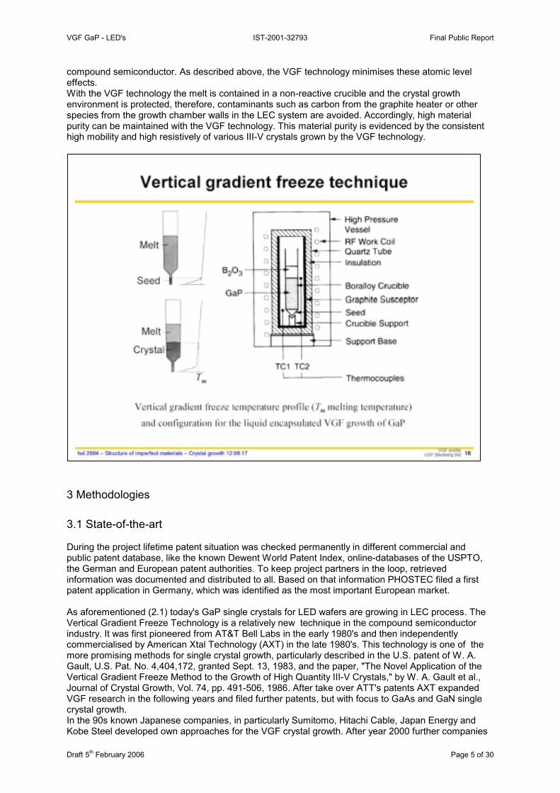
2.2 How does VGF work ? The VGF technology uses an enclosed crucible to hold the melt. The growth starts with a seed placed at the bottom of the crucible. Crystal growth is initiated by reducing the power input to the furnace, which in turn forces the solidification front to move upward. The motion of the solidification front is controlled by pre-programmed instructions to the fully automated furnace. Because the temperature gradient used in the VGF process is significantly lower than the Liquid-encapsulated Czochralski (LEC) process, this enables to grow crystals that have a relatively low dislocation density and high uniformity. In addition, with a low temperature gradient across the growth interface and a "hot on top" stable thermal environment, the melt turbulent convection is minimal with the VGF technology. This advantage enhances the uniform dopant incorporation and minimal growth striations in the VGF-grown crystals. The stechiometry of the VGF melt is protected by the vapours during the growth and therefore, the stechiometry of the VGF crystal is better controlled than crystals using the LEC technique. Material characteristics such as III-V-vacancies, twins and other defects with abnormal crystalline state, which are strongly influenced by the III/V ratio, are intimately related to the electrical properties of the
VGF GaP - LED's IST-2001-32793 Final Public Report
D
compound semiconductor. As described above, the VGF technology minimises these atomic level effects. With the VGF technology the melt is contained in a non-reactive crucible and the crystal growth environment is protected, therefore, contaminants such as carbon from the graphite heater or other species from the growth chamber walls in the LEC system are avoided. Accordingly, high material purity can be maintained with the VGF technology. This material purity is evidenced by the consistent high mobility and high resistively of various III-V crystals grown by the VGF technology.
3
3 Dptip AVicmGVJVcIK
raft 5th February 2006 Page 5 of 30
Methodologies
.1 State-of-the-art
uring the project lifetime patent situation was checked permanently in different commercial and ublic patent database, like the known Dewent World Patent Index, online-databases of the USPTO, he German and European patent authorities. To keep project partners in the loop, retrieved nformation was documented and distributed to all. Based on that information PHOSTEC filed a first atent application in Germany, which was identified as the most important European market.
s aforementioned (2.1) today's GaP single crystals for LED wafers are growing in LEC process. The ertical Gradient Freeze Technology is a relatively new technique in the compound semiconductor
ndustry. It was first pioneered from AT&T Bell Labs in the early 1980's and then independently ommercialised by American Xtal Technology (AXT) in the late 1980's. This technology is one of the ore promising methods for single crystal growth, particularly described in the U.S. patent of W. A. ault, U.S. Pat. No. 4,404,172, granted Sept. 13, 1983, and the paper, "The Novel Application of the ertical Gradient Freeze Method to the Growth of High Quantity III-V Crystals," by W. A. Gault et al., ournal of Crystal Growth, Vol. 74, pp. 491-506, 1986. After take over ATT's patents AXT expanded GF research in the following years and filed further patents, but with focus to GaAs and GaN single rystal growth. n the 90s known Japanese companies, in particularly Sumitomo, Hitachi Cable, Japan Energy and obe Steel developed own approaches for the VGF crystal growth. After year 2000 further companies
VGF GaP - LED's IST-2001-32793 Final Public Report
Draft 5th February 2006 Page 6 of 30
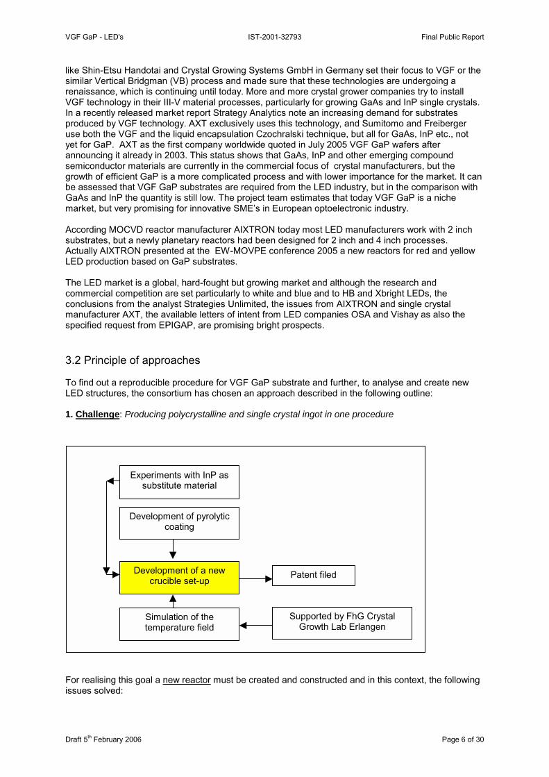
like Shin-Etsu Handotai and Crystal Growing Systems GmbH in Germany set their focus to VGF or the similar Vertical Bridgman (VB) process and made sure that these technologies are undergoing a renaissance, which is continuing until today. More and more crystal grower companies try to install VGF technology in their III-V material processes, particularly for growing GaAs and InP single crystals. In a recently released market report Strategy Analytics note an increasing demand for substrates produced by VGF technology. AXT exclusively uses this technology, and Sumitomo and Freiberger use both the VGF and the liquid encapsulation Czochralski technique, but all for GaAs, InP etc., not yet for GaP. AXT as the first company worldwide quoted in July 2005 VGF GaP wafers after announcing it already in 2003. This status shows that GaAs, InP and other emerging compound semiconductor materials are currently in the commercial focus of crystal manufacturers, but the growth of efficient GaP is a more complicated process and with lower importance for the market. It can be assessed that VGF GaP substrates are required from the LED industry, but in the comparison with GaAs and InP the quantity is still low. The project team estimates that today VGF GaP is a niche market, but very promising for innovative SME’s in European optoelectronic industry. According MOCVD reactor manufacturer AIXTRON today most LED manufacturers work with 2 inch substrates, but a newly planetary reactors had been designed for 2 inch and 4 inch processes. Actually AIXTRON presented at the EW-MOVPE conference 2005 a new reactors for red and yellow LED production based on GaP substrates. The LED market is a global, hard-fought but growing market and although the research and commercial competition are set particularly to white and blue and to HB and Xbright LEDs, the conclusions from the analyst Strategies Unlimited, the issues from AIXTRON and single crystal manufacturer AXT, the available letters of intent from LED companies OSA and Vishay as also the specified request from EPIGAP, are promising bright prospects. 3.2 Principle of approaches To find out a reproducible procedure for VGF GaP substrate and further, to analyse and create new LED structures, the consortium has chosen an approach described in the following outline: 1. Challenge: Producing polycrystalline and single crystal ingot in one procedure For realising this goal a new reactor must be created and constructed and in this context, the following issues solved:
Experiments with InP as substitute material
Development of a new crucible set-up
Simulation of the temperature field
Supported by FhG Crystal Growth Lab Erlangen
Development of pyrolytic coating
Patent filed
VGF GaP - LED's IST-2001-32793 Final Public Report
Draft 5th February 2006 Page 7 of 30
Firstly: To ensure and cover a wide field of experiments with crystal growth under low cost conditions it is necessary to use in addition to GaP related materials like InP (indium phosphide) too to gain insight in growing processes and obtain a huge volume of data for drawing inputs for GaP crystal growth. Since InP is related to GaP especially in lattice structures and temperature behaviour the material is well-appropriated to provide a first approach for GaP growing process control in particular, to prepare the single crystal growing from the polycrystalline and synthesis of polycrystalline material from input elements to the single crystal ingot in one continuous process. Secondly: To avoid any chemical reactions between the growing materials and the crucible wall materials and to avoid any contamination in reaction space during the growing process a specific pyrolytic coating for the inner surface was developed and in process tested by PHOSTEC. This pyrolytic coating is a PHOSTEC by-product respectively service resulting from developing the new crucible and especially applicable for users dealing with corrosive substances like in the chemical and environmental industries. Thirdly: To generate a field of temperature stimulating GaP single crystal growth numbers of heaters, the geometrical form of heaters, their surrounding, the distribution of heater and their heat outputs are needed precisely to calculate and install. Therefore, in co-operation with the Fraunhofer-Institute of Integrated Systems and Device Technology (Crystal Lab) in Erlangen (Germany) a simulation of the field of temperature was successfully carried out. Analytical results drawn out from the volume of data coming from the InP experiments, experiences with pyrolytic coating and outcomes from the computer simulation were taken jointly with the achievements of GaP growth into the creation and construction process for a new specific crystal growth set-up. These crystal growth equipment innovations are patented. This know how and new equipment is the base to define the reproducible data set for the VGF GaP growing procedure which will be completed process by process, beyond the project end too. 2. Challenge: Approaching to a new LED structure based on the VGF GaP substrate In close context with the development of new VGF GaP material it opens up the issue for new LED structure based on the VGF GaP substrate. The consortium has decided to investigate MOVPE growth for VGF GaP substrate in connection with epi-layers and hetero-structures targeted to optimising GaP based LED structures for improving light generation efficiency. Main emphasis of the project work were: • development of a MOVPE growth on substrate and an optimal doping level for quaternary systems
and • gaining knowledge and modelling a new type of homo and hetero-structures based on GaP/GaP,
GaP(N)/GaP and GaAs/AlGaInP/GaP for LED device design. Investigations have led to a new LED approach and the partners SAS and FEI STU could find a new way to create LED structures based on direct growth on GaP substrate. 3. Challenge: proofing of the new VGF GaP substrate by direct users To validate the VGF GaP substrate close by industry the consortium has chosen the following three-step method:
• Industrial usability test of epi-ready wafers • Testing by prototyping LEDs • Industrial usability test by sensor-LED-chip integrators This procedure allows to analyse the material along the processing chain and subsequently, to correct process parameters in the relevant pre-stages.
VGF GaP - LED's IST-2001-32793 Final Public Report
Draft 5th February 2006 Page 8 of 30
For supporting this validation method a specific industrial user group was established. Members are:
Industrial substrate usability test by material labs: Max-Planck-Institut für Mikrostrukturphysik Halle, OSA Berlin
Industrial usability test by epitaxy by European epilayer producers: Epinova, Freiburg FhG AFP, Freiburg MaTecK, Juelich Freiberger Compound Materials III/V Epitaxial Service AG, Berlin
Testing by prototyping LED by European LED manufacturers: OSA Berlin Vishay-Opto-Fab, Heilbronn
By letters of intent the members have reinforced that they are also interested to validate the new VGF GaP substrate beyond the official project end. 4 Project results
4.1 Target focussing In close co-operation with potential users in particular with members of the industrial user group the project team has rendered more precisely the requirements specifications for VGF GaP substrate during the project duration. Driven by interested parties the consortium envisages the following panel for VGF GaP Parameters/technical characteristics Specification required conductivity type n or p N EPD should be < 103 / cm2
Sides polished will be one side polished diameter will be 50 and 74 mm thickness according requirements in the range 0,3 - 0,5 mm crystal orientation now in [111] direction, later on in [100] resistively should be max. 0,2 ohm - cm dopant S Originally, the target groups comprised only • Direct users of GaP substrate, epi-ready wafers and LED manufacturers and • industrial LED application research units.
In result of increasing penetration of the market the consortium has decided to add potential users from niche market sectors like optical components. The main reason leading to extension of the target group is caused by limitation of recent PHOSTEC capabilities as contractor of VGF GaP epi-ready wafers. Consequently, PHOSTEC intents to co-operate (networking) with wafer processing companies (crystal post-processing) to fulfil requirements of costumers to ensure a fast time to market, lower costs and high flexibility, which is the base for reaching a good competitive position. It should be highlighted that the project team has developed the new VGF method for GaP in 42 months in connection with a cost efficiency of 2T€ per person month.
VGF GaP - LED's IST-2001-32793 Final Public Report
Draft 5th February 2006 Page 9 of 30
4.2 Achievements In close co-operation with the potential user community the project team has drawn a lot of experiences in crystal growth especially related to GaP and InP as substitute material, further in GaP growth chamber construction in particular to overcome the problems arising from the needed high pressure phosphorous vapour atmosphere during the crystal growth process. This benefit is the result coming from the internal and external co-operation with competent partners developed by the project management over the whole project duration. The achieved high collaboration level between the consortium, crystal labs and user industries gives an excellent guarantee for successful completing the VGF GaP substrate experiments according to the user-specific parameter panel (see section 4.1). The main achievements can be summarised as follows: • Improved synthesis of semiconductor phosphides as GaP and InP, probably could be used new
name here: VGF synthesis of GaP and InP • Pyrolytic deposition of PG, PBN and PSi3N4 layers • Development of the VGF GaP process and crystal growth apparatus • New VGF GaP substrate • Experiences in homo and heterostructures for LED device design • Directly grown GaP LEDs • New experiences with the MOVPE procedure • Management of co-operation between a R&D team and industrial user group
4.3 Raising awareness This section describes the dissemination and exploitation strategies, actions and specific measures jointly prepared and organised by all partners based on a project-specific dissemination and use plan (2). It defines a practical course to reach the market, for the mentioned main target groups • LED manufacturing industry, • industrial LED application research units which can draw an essential added value from the new
GaP substrate and • optical industries interested to use VGF GaP material for advanced optical components (e.g.
lenses, solar cells), and on the other hand, to gain benefit from the industries for improving the crystal growing process and further, for early focussing the new VGF material on the market and benefits coming from new applications. Consequently, the consortium has established the industrial user group to form a specific partnership to close the feedback loop to GaP substrate processing. During the project duration the targeted dissemination and use activities led to following selected results respective benefit: • An electronic mailing list comprising more than 160 contacts
(reseller, wafer finishing companies, academic units and crystal growth labs, LED manufacturers, equipment suppliers, multipliers etc.) world-wide to spread up the latest news about VGF GaP material.
• Establishing an industrial user group comprising LED labs, epi-ready wafers producers and LED
manufacturers (see section 3.2) and long-term co-operation offers from selected members manifested by letters of intent like OSA Berlin and Vishay-Opto-fab Heilbronn (Germany).
• Involvement into the "Deutsche Gesellschaft für Kristallographie" (German Association for Crystallography) and its industrial working groups via co-operation agreement with the Fraunhofer-Institute of Integrated systems and Device Technology, Crystal Lab, in Erlangen.
VGF GaP - LED's IST-2001-32793 Final Public Report
Draft 5th February 2006 Page 10 of 30
Furthermore, in result of these activities Phostec is in the meantime a well-know III/V-material provider accepted by the crystal growth community and European direct epi-ready wafer users.
• Opening a potential co-operation line with OSRAM Opto Semiconductors GmbH for the use of
VGF GaP substrate in result of direct contacts to the marketing management.
• Finding out market sectors for the use of the new developed VGF GaP material being expected coming along well in the next years in result of detailed discussions with potential applicants and scientists, like for optical lenses, semiconductor lasers and solar cells.
• Pre-enquires in detail for delivery of VGF GaP substrate showing the material need related to LED
market for example from : Protech Ltd. Korea, Epigap Berlin and Vishay Heilbronn (both Germany). and pre-enquiries from niche market segments, for example Philips-University Marburg and from Fraunhofer Institute IOF Jena (both Germany).
In particular, as a result of a targeted project website (3), articles in scientific and business magazines, press releases and electronic newsletter about the project progress, organising direct contacts, company and lab visits to potential applicants, epi-ready wafer users and LED manufacturers and, participating actively in Technology Days and Brokerage events like "Material Forum" at the Hanover fair 2005 or Laser-Optik Berlin (March 2004), the project established a pool of co-operation partners and potential users for further development in VGF GaP crystal growth. An overall overview about all activities undertaken and organised is covered in the project specific dissemination and use plan (2).
4.5 Impact with the technical prospect The VGF method undergoes presently a renaissance and is today an emerging technology for the growth of various compound semiconductor single crystals and with increasing market value in optoelectronics industry. So the achievements of the projects relating growth of GaP single crystal are also relevant for the development of InP and GaAs devices, for high-brightness (HB) LEDs, optical function components and solar cells. The huge experiences attained in scientific and technical experiments perform strongly conditions and are excellent references for further research in crystal growth and development of advances LED devices. In this context it is worth to emphasize the new epi-layer LED structures, investigated in the project for high efficiency green colour LEDs based on GaP substrate. Advanced GaP substrate with benefits in an essential lower dislocation density, a more homogenous doping quality and certainly the transparency of this material are required material features and can assist market growth. The great efforts of big players, like AIXTRON, Vishay and Epigap in Europe and certainly the crystal companies in Asia are showing the current awareness of VGF and GaP. The currently rapid development of LED materials and devices challenges corporations and competitors. A flexible and highly committed SME, like PHOSTEC can enter the market with costumer orientation, lower costs at better and reliable quality and adherence to delivery dates. 5 Outcomes 5.1 Improved synthesis (VGF synthesis) of polycrystalline indium phosphide InP
and gallium phosphide GaP The very first step in the compound semiconductor material production is the synthesis of the polycrystalline GaP and InP ingots. This operation is the birthplace, where under the special pressure and temperature conditions the single materials as the gallium or indium and the phosphorus are connected together and the material with new parameters called GaP or InP is created. Usually the research equipment, needed for the synthesis, is made partially from the quartz glass, and the capacity of the such equipment is in the range of 10 kg per year. But the industry demand is several hundreds or thousands of the kg of the polycrystalline ingots per production unit annually, and this capacity usually could be reached only with special metallic high pressure synthesis reactor.
VGF GaP - LED's IST-2001-32793 Final Public Report
Draft
The synthesis chemical reaction is very simple and for InP could be described as follows: 4 In(l) + P4(g) = 4 InP(l) 2 In(l) + P2(g) = 2 InP(l) or in case of GaP: 4 Ga(l) + P4(g) = 4 GaP(l) 2 Ga(l) + P2(g) = 2 GaP(l)
Maybe one can asks, when the reaction is so simple, why the special task is devoted to synthesis development within the frame of project?
The answer is, that at the end of this simple reaction there never will be 100 % pure InP or GaP, but still there will exist some quantity of unreacted In resp. Ga.
The short chemical engineering analysis can show us, that for example in case of GaP synthesis if we suddenly frees the melt, then we shall find out in material, that there will be GaP equal approximately to 6/7 of total quantity, and Ga will be in the range of 1/7 of total quantity. The only way how to produce pure GaP is to force axial temperature gradient in the melt, which will induce segregation of GaP on colder side of melt. In the same time the phosphorus content in the melt is lowered and the melt is able to absorb new phosphorus gas.
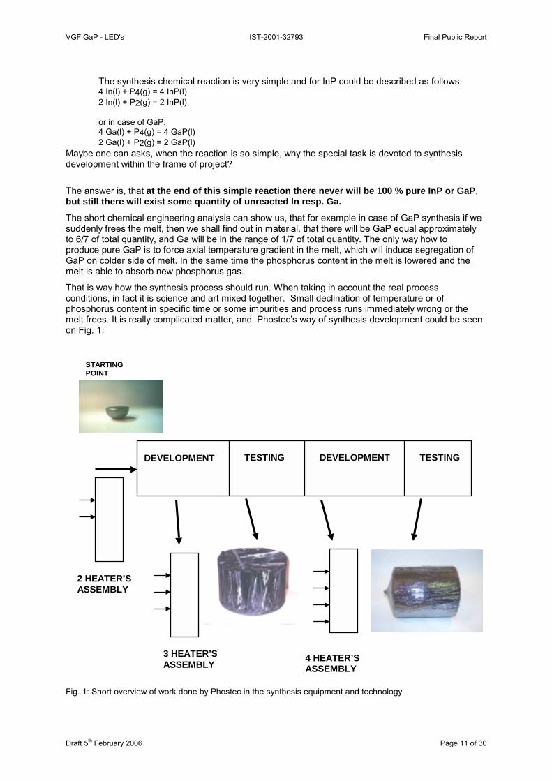
That is way how the synthesis process should run. When taking in account the real process conditions, in fact it is science and art mixed together. Small declination of temperature or of phosphorus content in specific time or some impurities and process runs immediately wrong or the melt frees. It is really complicated matter, and Phostec’s way of synthesis development could be seen on Fig. 1: Fig.
STARTING
2A
POINT
5th February 2006
1: Short overview of work done by Phostec in the synthesi
DEVELOPMENT DEVELOPMENT
TESTING
TESTING
HEATER’S SSEMBLY
3 HEATER’S ASSEMBLY
4 HEATER’S ASSEMBLY
Page 11 of 30
s equipment and technology

VGF GaP - LED's IST-2001-32793 Final Public Report
Draft 5th February 2006 Page 12 of 30
Some reached results are displayed on Fig. 2 and Fig. 3:
(a) InP 8,25 kg (b) InP 10,13 kg Fig. 2: Cross-section view of InP ingots prepared with measurement of temperature in the reaction zone, diameter of both ingots is 130 mm.
(a) GaP 7,21 kg, Φ 130 mm (b) GaP 8,97 kg, Φ 150 mm Fig. 3: Cross-section view of GaP ingots prepared in different crucibles.

VGF GaP - LED's IST-2001-32793 Final Public Report
Draft 5th February 2006 Page 13 of 30
When evaluating the reached level of technology, it could be said:
1) presented polycrystalline synthesis technology belongs probably to very promising in the world while ingots developing in project have weight 5 – 10 kg, and same offered on market are usually in range 1 – 3 kg;
2) only weight itself is not so important, but Phostec bigger ingots bring higher productivity of work, that influence the costs and help to decrease the price approximately to 50 – 70 %, and that is already advantage for single crystal growth and for customers;
3) and what the most important thing is, that developed synthesis process in fact join 2 processes: synthesis itself and VGF cooling of material, and that add value to and increase quality of material, so it could be classified as “re-pulled” (usually the re-pulled polycrystalline material is at first synthesised and then pulled for example with Czochralski method), that means free of any cracks and defects with look of solid piece of metal.
5.2 Pyrolytic deposition of PG, PBN and PSi3N4 layers GaP synthesis and single crystal growth take place at very high temperatures. The melting point of GaP is 1457 °C, but for successful solidification process a temperature gradient in range of 200 °C is needed along the crucible axis. Therefore maximal working temperature arises up to 1700 °C.
This is very severe condition, while at this temperature many materials evaporate already. But crystal growth process need high purity of reaction space, of course, no evaporation of any material is allowed, otherwise GaP will be contaminated. For to fulfil these requirements a parts made from high purity graphite are used. They are covered with different protective layers for to interrupt the undesirable chemical reaction, which could lead to contamination of melt. At the beginning of project Phostec had tried to purchase the service – the deposition of protective layers, but shortly it had shown up, that this is not correct way. The high price, long delivery times and especially the requirement, that only new graphite parts could be deposited, lead finally to decision to develop own deposition technology.
This step was successful realised and today has Phostec to disposition the following deposition technologies:
- deposition of pyrolytic graphite (PG) protective layers – the thickness is in the range of 0,01 – 0,03 mm,
- deposition of pyrolytic boron nitride (PBN) protective layers, here the thickness is higher up to 0,1 – 0,2 mm,
- deposition of pyrolytic silicium nitride (PSi3N4) protective layers, these layers are again very thin – about 0,01 mm – due to high coefficient of thermal extension.
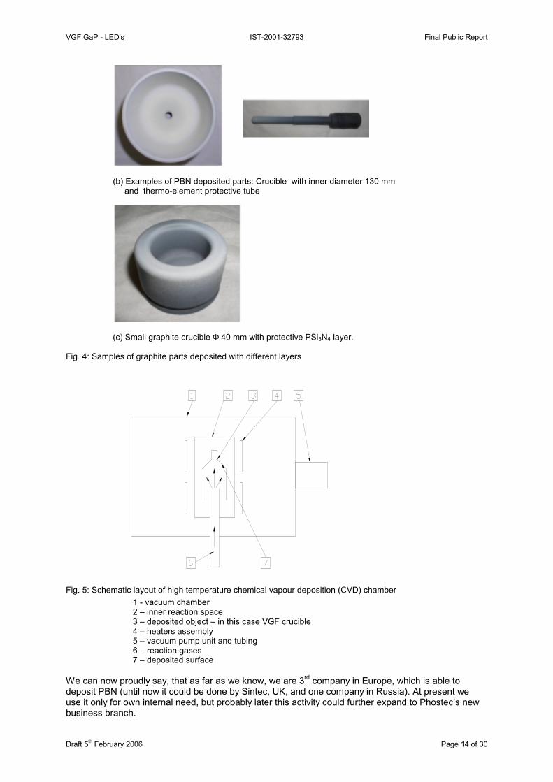
Some examples of different deposited parts could be seen on the Fig. 4. The schematically is the deposition process displayed on Fig. 5.
(a) Graphite parts deposited with PG layers
VGF GaP - LED's IST-2001-32793 Final Public Report
Draft 5th February 2006 Page 14 of 30
(b) Examples of PBN deposited parts: Crucible with inner diameter 130 mm and thermo-element protective tube
(c) Small graphite crucible Φ 40 mm with protective PSi3N4 layer.
Fig. 4: Samples of graphite parts deposited with different layers
Fig. 5: Schematic layout of high temperature chemical vapour deposition (CVD) chamber 1 - vacuum chamber 2 – inner reaction space 3 – deposited object – in this case VGF crucible 4 – heaters assembly 5 – vacuum pump unit and tubing 6 – reaction gases 7 – deposited surface
We can now proudly say, that as far as we know, we are 3rd company in Europe, which is able to deposit PBN (until now it could be done by Sintec, UK, and one company in Russia). At present we use it only for own internal need, but probably later this activity could further expand to Phostec’s new business branch.

VGF GaP - LED's IST-2001-32793 Final Public Report
Draft 5th February 2006 Page 15 of 30
Worthwhile are at least 2 aspects of owing the deposition technology:
- speed of development is considerable, there is certainly not so many companies in world, where for example when decision on new type of crucible is taken on Monday, on Tuesday run the production of graphite crucible, on Wednesday is realised PBN deposition, and on Thursday this crucible could be installed in crystal growth process;
- development costs are very reasonable, until now we have made 88 PG depositions and 105 PBN depositions, that means we have saved on our research costs at least 50.000 – 100.000 EUR. The PSi3N4 deposition is not used too much, only several sample processes were realised.
5.3 Development of the VGF GaP process and crystal growth apparatus
GaP crystal growth based on phosphorous injection Principally exists 2 possibilities how to maintain the phosphorous vapour pressure during crystal growth process. One of them is injection of phosphorous gas in the melt. The advantage of this method is, that eventual contamination of melt surface with oxides is no problem. For another method, based on the reaction of phosphorous gas with Ga through melt surface, such contamination creates principal problem and some traces of oxides can totally break the reaction. For example melting point of Ga2O3 is 1740 oC, it creates very easy and it floats on surface of melt.
We have met the oxide problem many time before, therefore we have tried to solve it by injection of phosphorous in Ga/GaP melt. Schematic diagram of technology is displayed on Fig. 6.
Fig. 6: Schematic diagram of phosphorous injection in the melt
1 – heaters assembly 2 – temperature measurement exactly in reaction place 3 – phosphorous tube 4 – phosphorous gas 5 – Ga / GaP melt (tested also for In / InP) 6 – cover layer of melted B2O3
We have designed and manufactured all needed graphite assembly and after some preparation we have realised 2 GaP processes and 2 InP processes. The results were not successful, so we have stopped further work because of:
1) we could not reach required stechiometric composition of melt (well later on we have found out some improvement in phosphorous sublimation, so maybe now the results could be different);
2) we could not reach required temperature gradient in the melt (again, now when we are able to mathematically model processes in melt, the solution could be other).
VGF GaP - LED's IST-2001-32793 Final Public Report
Draft 5th February 2006 Page 16 of 30
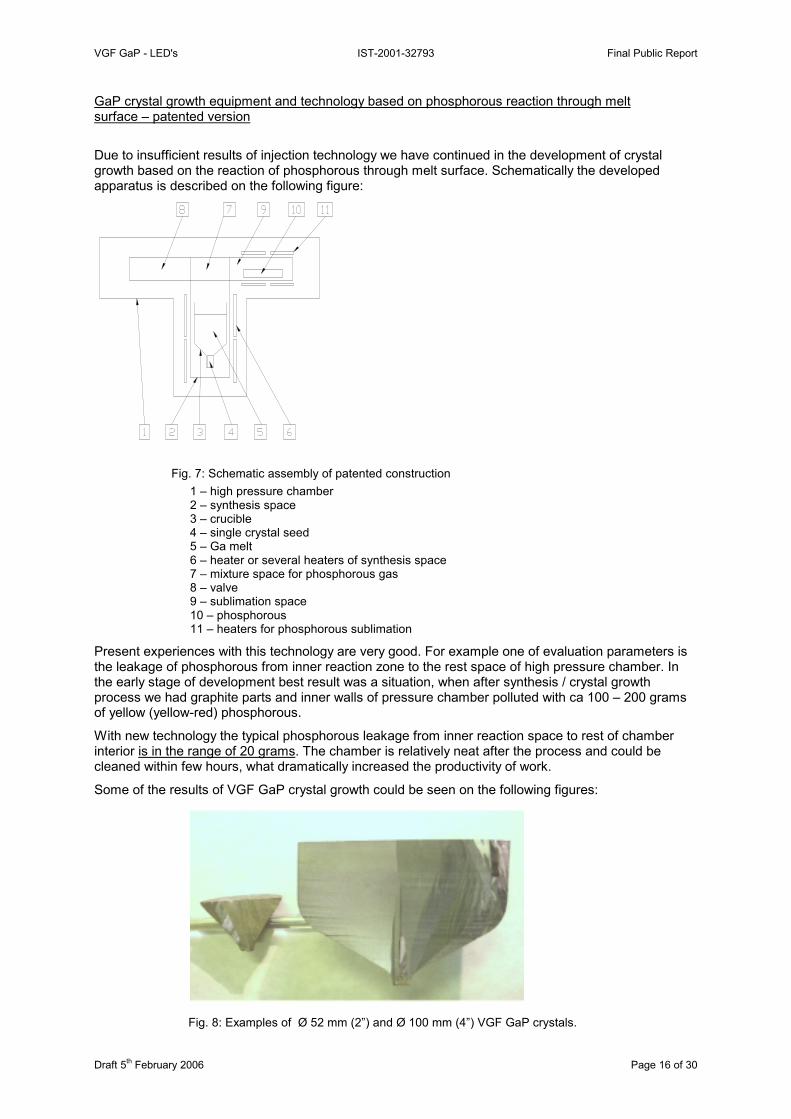
GaP crystal growth equipment and technology based on phosphorous reaction through melt surface – patented version
Due to insufficient results of injection technology we have continued in the development of crystal growth based on the reaction of phosphorous through melt surface. Schematically the developed apparatus is described on the following figure:
Fig. 7: Schematic assembly of patented construction
1 – high pressure chamber 2 – synthesis space 3 – crucible 4 – single crystal seed 5 – Ga melt 6 – heater or several heaters of synthesis space 7 – mixture space for phosphorous gas 8 – valve 9 – sublimation space 10 – phosphorous 11 – heaters for phosphorous sublimation
Present experiences with this technology are very good. For example one of evaluation parameters is the leakage of phosphorous from inner reaction zone to the rest space of high pressure chamber. In the early stage of development best result was a situation, when after synthesis / crystal growth process we had graphite parts and inner walls of pressure chamber polluted with ca 100 – 200 grams of yellow (yellow-red) phosphorous.
With new technology the typical phosphorous leakage from inner reaction space to rest of chamber interior is in the range of 20 grams. The chamber is relatively neat after the process and could be cleaned within few hours, what dramatically increased the productivity of work.
Some of the results of VGF GaP crystal growth could be seen on the following figures:
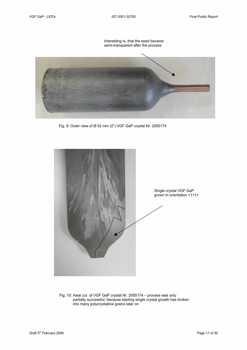
Fig. 8: Examples of Ø 52 mm (2”) and Ø 100 mm (4”) VGF GaP crystals.
VGF GaP - LED's IST-2001-32793 Final Public Report
Draft 5th February 2006
Interesting is, that the seed became
semi-transparent after the process Fig. 9: Outer view of Ø 52 mm (2”) VGF GaP crystal Nr. 2005174
Fig. 10: Axial cut of VGF GaP crystal Nr. 2005174 – pro partially successful, because starting single crys into many polycrystalline grains later on
Single crystal VGF GaP grown in orientation <111>
Page 17 of 30
cess was only tal growth has broken
VGF GaP - LED's IST-2001-32793 Final Public Report
Draft 5th Fe
5.4 Ne
This projpurposes
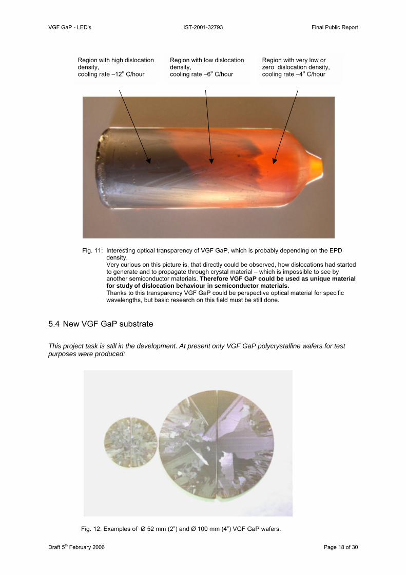
Region with high dislocationdensity, cooling rate –12o C/hour
bruary 2006
Fig. 11: Interesting optical trandensity. Very curious on this pto generate and to proanother semiconductofor study of dislocatiThanks to this transpawavelengths, but basi
w VGF GaP substrate
ect task is still in the developm were produced:
Fig. 12: Examples of Ø 52 mm
Region with low dislocationdensity, cooling rate –6o C/hour
sparency of VGF GaP, which is p
icture is, that directly could be obspagate through crystal material –r materials. Therefore VGF GaP on behaviour in semiconductorrency VGF GaP could be perspecc research on this field must be st
ent. At present only VGF GaP
(2”) and Ø 100 mm (4”) VGF GaP
Region with very low or zero dislocation density,cooling rate –4o C/hour
Page 18 of 30
robably depending on the EPD
erved, how dislocations had started which is impossible to see by could be used as unique material materials. tive optical material for specific ill done.
polycrystalline wafers for test
wafers.
VGF GaP - LED's IST-2001-32793 Final Public Report
Draft 5th February 2006 Page 19 of 30
As mentioned already before, the research work on further development of VGF GaP single crystal growth will continue also beyond official project timetable. The aim is to produce with good repeatability Ø 52 mm (2”) VGF GaP wafers and to test the technological possibilities by preparation of samples of Ø 75 mm (3”) and Ø 100 mm (4”) VGF GaP wafers.
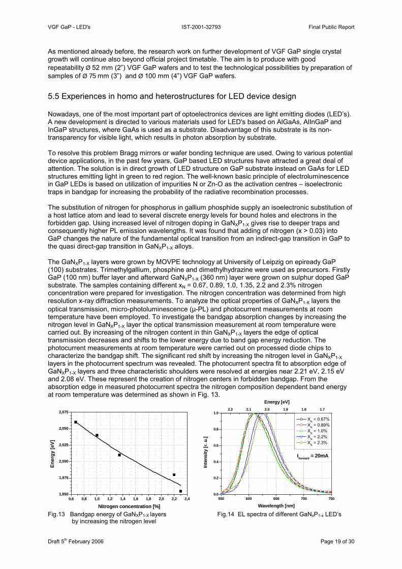
5.5 Experiences in homo and heterostructures for LED device design Nowadays, one of the most important part of optoelectronics devices are light emitting diodes (LED’s). A new development is directed to various materials used for LED's based on AlGaAs, AlInGaP and InGaP structures, where GaAs is used as a substrate. Disadvantage of this substrate is its non-transparency for visible light, which results in photon absorption by substrate. To resolve this problem Bragg mirrors or wafer bonding technique are used. Owing to various potential device applications, in the past few years, GaP based LED structures have attracted a great deal of attention. The solution is in direct growth of LED structure on GaP substrate instead on GaAs for LED structures emitting light in green to red region. The well-known basic principle of electroluminescence in GaP LEDs is based on utilization of impurities N or Zn-O as the activation centres – isoelectronic traps in bandgap for increasing the probability of the radiative recombination processes. The substitution of nitrogen for phosphorus in gallium phosphide supply an isoelectronic substitution of a host lattice atom and lead to several discrete energy levels for bound holes and electrons in the forbidden gap. Using increased level of nitrogen doping in GaNXP1-X gives rise to deeper traps and consequently higher PL emission wavelengths. It was found that adding of nitrogen (x > 0.03) into GaP changes the nature of the fundamental optical transition from an indirect-gap transition in GaP to the quasi direct-gap transition in GaNXP1-X alloys. The GaNXP1-X layers were grown by MOVPE technology at University of Leipzig on epiready GaP (100) substrates. Trimethylgallium, phosphine and dimethylhydrazine were used as precursors. Firstly GaP (100 nm) buffer layer and afterward GaNXP1-X (360 nm) layer were grown on sulphur doped GaP substrate. The samples containing different xN = 0.67, 0.89, 1.0, 1.35, 2.2 and 2.3% nitrogen concentration were prepared for investigation. The nitrogen concentration was determined from high resolution x-ray diffraction measurements. To analyze the optical properties of GaNXP1-X layers the optical transmission, micro-photoluminescence (µ-PL) and photocurrent measurements at room temperature have been employed. To investigate the bandgap absorption changes by increasing the nitrogen level in GaNXP1-X layer the optical transmission measurement at room temperature were carried out. By increasing of the nitrogen content in thin GaNXP1-X layers the edge of optical transmission decreases and shifts to the lower energy due to band gap energy reduction. The photocurrent measurements at room temperature were carried out on processed diode chips to characterize the bandgap shift. The significant red shift by increasing the nitrogen level in GaNXP1-X layers in the photocurrent spectrum was revealed. The photocurrent spectra fit to absorption edge of GaNXP1-X layers and three characteristic shoulders were resolved at energies near 2.21 eV, 2.15 eV and 2.08 eV. These represent the creation of nitrogen centers in forbidden bandgap. From the absorption edge in measured photocurrent spectra the nitrogen composition dependent band energy at room temperature was determined as shown in Fig. 13.
0,6 0,8 1,0 1,2 1,4 1,6 1,8 2,0 2,2 2,41,950
1,975
2,000
2,025
2,050
2,075
Ener
gy [e
V]
Nitrogen concentration [%] 550 600 650 700 750
0.0
0.2
0.4
0.6
0.8
1.02.2 2.1 2.0 1.9 1.8 1.7
Iforward = 20mA
Inte
nsity
[r. u
.]
Wavelength [nm]
XN = 0.67% XN = 0.89% XN = 1.0% X
N = 2.2%
XN = 2.3%
Energy [eV]
Fig.13 Bandgap energy of GaNXP1-X layers Fig.14 EL spectra of different GaNxP1-x LED’s
by increasing the nitrogen level
VGF GaP - LED's IST-2001-32793 Final Public Report
Draft 5th February 2006 Page 20 of 30
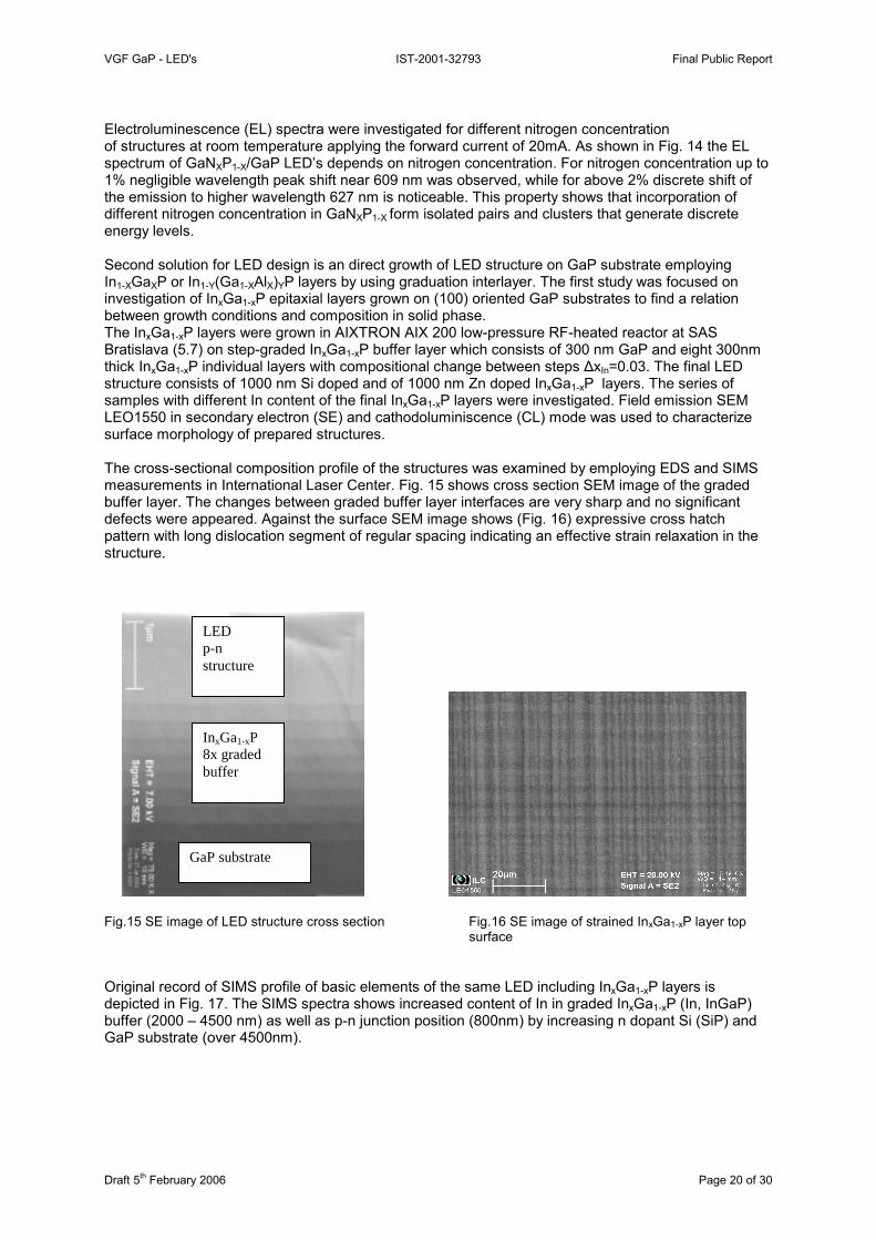
Electroluminescence (EL) spectra were investigated for different nitrogen concentration of structures at room temperature applying the forward current of 20mA. As shown in Fig. 14 the EL spectrum of GaNXP1-X/GaP LED’s depends on nitrogen concentration. For nitrogen concentration up to 1% negligible wavelength peak shift near 609 nm was observed, while for above 2% discrete shift of the emission to higher wavelength 627 nm is noticeable. This property shows that incorporation of different nitrogen concentration in GaNXP1-X form isolated pairs and clusters that generate discrete energy levels. Second solution for LED design is an direct growth of LED structure on GaP substrate employing In1-XGaXP or In1-Y(Ga1-XAlX)YP layers by using graduation interlayer. The first study was focused on investigation of InxGa1-xP epitaxial layers grown on (100) oriented GaP substrates to find a relation between growth conditions and composition in solid phase. The InxGa1-xP layers were grown in AIXTRON AIX 200 low-pressure RF-heated reactor at SAS Bratislava (5.7) on step-graded InxGa1-xP buffer layer which consists of 300 nm GaP and eight 300nm thick InxGa1-xP individual layers with compositional change between steps ∆xIn=0.03. The final LED structure consists of 1000 nm Si doped and of 1000 nm Zn doped InxGa1-xP layers. The series of samples with different In content of the final InxGa1-xP layers were investigated. Field emission SEM LEO1550 in secondary electron (SE) and cathodoluminiscence (CL) mode was used to characterize surface morphology of prepared structures. The cross-sectional composition profile of the structures was examined by employing EDS and SIMS measurements in International Laser Center. Fig. 15 shows cross section SEM image of the graded buffer layer. The changes between graded buffer layer interfaces are very sharp and no significant defects were appeared. Against the surface SEM image shows (Fig. 16) expressive cross hatch pattern with long dislocation segment of regular spacing indicating an effective strain relaxation in the structure.
Fig.15 SE image of LED structure cross section Fig.16 SE image of strained InxGa1-xP layer top
surface Original record of SIMS profile of basic elements of the same LED including InxGa1-xP layers is depicted in Fig. 17. The SIMS spectra shows increased content of In in graded InxGa1-xP (In, InGaP) buffer (2000 – 4500 nm) as well as p-n junction position (800nm) by increasing n dopant Si (SiP) and GaP substrate (over 4500nm).
LED p-n structure
InxGa1-xP 8x graded buffer
GaP substrate
VGF GaP - LED's IST-2001-32793 Final Public Report
Draft 5th February 2006 Page 21 of 30
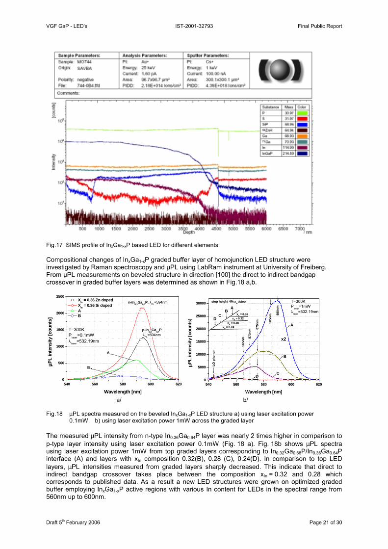
Fig.17 SIMS profile of InxGa1-xP based LED for different elements Compositional changes of InxGa1-xP graded buffer layer of homojunction LED structure were investigated by Raman spectroscopy and µPL using LabRam instrument at University of Freiberg. From µPL measurements on beveled structure in direction [100] the direct to indirect bandgap crossover in graded buffer layers was determined as shown in Fig.18 a,b.
540 560 580 600 6200
500
1000
1500
2000
2500
T=300KP
laser=0.1mW
λ laser=532.19nm
B
A
n-In0,3Ga0,7P, λPL
=594nm
p-In0,3Ga0,7Pλ
PL=594nm
XIn = 0.36 Zn doped XIn = 0.36 Si doped A B
µµ µµ PL
inte
nsity
[cou
nts]
Wavelength [nm]
540 560 580 600 6200
5000
10000
15000
20000
25000
30000
xN = 0.24xN = 0.28
xN = 0.32xN = 0.36
DC
BA
DC
B
A
T=300KPlaser=1mWλ
laser=532.19nm
LO p
hono
n
565n
m
590n
m
585n
m
570n
m 575n
m
step height 4% xIn /step
x2
µµ µµPL
inte
nsity
[cou
nts]
Wavelength [nm] a/ b/ Fig.18 µPL spectra measured on the beveled InxGa1-xP LED structure a) using laser excitation power 0.1mW b) using laser excitation power 1mW across the graded layer The measured µPL intensity from n-type In0.36Ga0.64P layer was nearly 2 times higher in comparison to p-type layer intensity using laser excitation power 0.1mW (Fig. 18 a). Fig. 18b shows µPL spectra using laser excitation power 1mW from top graded layers corresponding to In0.32Ga0.68P/In0.36Ga0.64P interface (A) and layers with xIn composition 0.32(B), 0.28 (C), 0.24(D). In comparison to top LED layers, µPL intensities measured from graded layers sharply decreased. This indicate that direct to indirect bandgap crossover takes place between the composition xIn = 0.32 and 0.28 which corresponds to published data. As a result a new LED structures were grown on optimized graded buffer employing InxGa1-xP active regions with various In content for LEDs in the spectral range from 560nm up to 600nm.
VGF GaP - LED's IST-2001-32793 Final Public Report
Draft 5th February 2006 Page 22 of 30
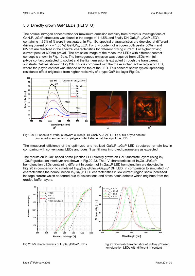
5.6 Directly grown GaP LEDs (FEI STU) The optimal nitrogen concentration for maximum emission intensity from previous investigations of GaNxP1-x/GaP structures was found in the range of 1-1.5% and finally DH GaNxP1-x/GaP LED’s containing 1.35% of N were investigated. In Fig. 19a spectral characteristics are depicted at different driving current of (x = 1.35 %) GaNxP1-x LED. For this content of nitrogen both peaks 609nm and 627nm are resolved in the spectral characteristics for different driving current. For higher driving current peak at 609nm prevail. The emission image of the measured LEDs with different contact concept is shown in Fig. 19b,c. The homogenous emission was acquired from LEDs with full p-type contact contacted to socket and the light emission is extracted through the transparent substrate GaP as shown in Fig 19b. This is compared with the mesa etched active region of LED, where the p-type contact was shaped at the top of the LED. This concept shows typical spreading resistance effect originated from higher resistivity of p-type GaP top layer Fig19c.
500 550 600 650 700 750 800
0
10
20
30
40
50
60
70
80
90
100
Inte
nsity
[a.u
.]
Wavelength [nm]
50 mA 40 30 20 10
GaNP/GaP LED, 1.35%609 nm627
750
78 nm
a/ b/ c/ Fig.19a/ EL spectra at various forward currents DH GaNxP1-x/GaP LED’s b/ full p-type contact contacted to socket and c/ p-type contact shaped at the top of the LED The measured efficiency of the optimized and realized GaNxP1-x/GaP LED structures remain low in comparing with conventional LEDs and doesn’t get till now improved parameters as expected. The results on InGaP based homo-junction LED directly grown on GaP substrate layers using In1-
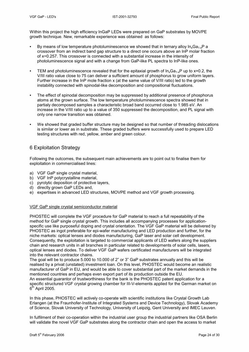
XGaXP graduation interlayer are shown in Fig.20-23. The I-V characteristics of InxGa1-xP/GaP homojunction LEDs containing different In content of InxGa1-xP LED homojunction are depicted in Fig. 20 in comparison to simulated In0.36Ga0.64P/In0.25Ga0.75P DH LED. In comparison to simulated I-V characteristics the homojunction InxGa1-xP LED characteristics in low current region show increased leakage current which appeared due to dislocations and cross hatch defects which originate from the graded buffer layers.
0.50 0.75 1.00 1.25 1.50 1.75 2.00
1E-6
1E-5
1E-4
1E-3
0.01
0.1
Forw
ard
curr
ent [
A]
Forward volatage [V]
xIn = 0.36 xIn = 0.32 xIn = 0.295 xIn = 0.36 simulated
525 550 575 600 6250.0
0.2
0.4
0.6
0.8
1.0
EL in
tens
ity [r
. u.]
Wavelength [nm]
xIn = 0.28
xIn = 0.295 xIn = 0.32 x
In = 0.36
Fig.20 I-V characteristics of InxGa1-xP/GaP LEDs Fig.21 Spectral characteristics of InxGa1-xP based homojunction LEDs with different In content

VGF GaP - LED's IST-2001-32793 Final Public Report
Draft 5th February 2006 Page 23 of 30
Typical EL spectra of different In content homojunction InxGa1-xP LED’s measured at 300K by Ocean Optics spectrometer are depicted in Fig.21. All of the measured EL emission spectra peaks from a different In content homojunction InxGa1-xP LED’s were in the range from 562nm to 596nm (at 30mA). These EL spectra peaks correspond to In content xIn = 0.28, 0.295, 0.32, 0.36 in active layer of investigated LEDs. A maximal measured optical power 40 µW/ 30mA was reached for LED sample with In content 36% in active region as shown in Fig 22a,b. LEDs light emission image is shown in for bottom up chip concept and emission through the transparent GaP substrate, where full p-type contact was prepared on the back side of the LED chip. Fig. 22b shows the detail focused on the bottom of the chip, where cross hatch defects appears.
a/ b/ Fig. 22a,b LED emission image of In0.36Ga0.64P active layer composition for bottom up concept By decreasing In content in InxGa1-xP (x = 0.32 and 0.3) active layer near to direct – indirect bandgap transition (xIn~0.29) emitted optical power is decreasing as well as emitted wavelength. It could be seen on the next Fig 23a,b:
a/ b/ Fig. 23 LED emission image of active layer composition a/ In0.32Ga0.68P and b/ In0.29Ga0.71P The first measured results on InGaP LED with graduation interlayer structure show promising emission intensity comparable with conventional GaP LED’s and single emission peak in the range of 560-590 nm with FWHM value of ~25 nm corresponding to different InxGa1-xP composition in the range of x=0.29 – 0.36. 5.7 New experiences with the MOVPE procedure Light emitting diodes (LEDs) belong to a group of the oldest optoelectronic devices that took the initiative in the development of III-V semiconductors. LED research has currently seen a renaissance period. Progress both in the technology of LEDs and materials has allowed for a shift in LED application from signal and information processing to lighting. The most widespread type of high-brightness LED is based on an MOCVD-grown structure with a light-emitting PN junction formed in the AlGaInP quaternary whose composition makes it lattice matched to GaAs substrate. However, GaAs substrate absorbs a considerable part of radiation emitted in the active part of the LED structure. This absorption can be eliminated by replacing of the GaAs substrate with GaP. In this case it is necessary to insert between the substrate and the active region an intermediate layer structure (so called „buffer“) enabling the change of the lattice constant from the substrate to the final active layer. This structure is realized from ternary alloy InxGa1-xP with increasing amount of In. Very important function of this structure is to change band gap energy so that a green colour luminescence may be reached. Another very important property is to be able to filter the dislocations propagation from substrate to the electroluminescent part of the LED structure.
VGF GaP - LED's IST-2001-32793 Final Public Report
Draft 5th February 2006 Page 24 of 30
Within this project the high efficiency InGaP LEDs were prepared on GaP substrates by MOVPE growth technique. New, remarkable experience was obtained as follows: • By means of low temperature photoluminescence we showed that in ternary alloy InxGa1-xP a
crossover from an indirect band gap structure to a direct one occurs above an InP molar fraction of x=0.257. This crossover is connected with a substantial increase in the intensity of photoluminescence signal and with a change from GaP-like PL spectra to InP-like ones.
• TEM and photoluminescence revealed that for the epitaxial growth of InxGa1-xP up to x=0.2, the
V/III ratio value close to 75 can deliver a sufficient amount of phosphorus to grow uniform layers. Further increase in the InP mole fraction x (at the same value of V/III ratio) led to the growth instability connected with spinodal-like decomposition and compositional fluctuations.
• The effect of spinodal decomposition may be suppressed by additional presence of phosphorus
atoms at the grown surface. The low temperature photoluminescence spectra showed that in partialy decomposed samples a characteristic broad band occurred close to 1.985 eV. An increase in the V/III ratio up to a value of 350 suppressed the decomposition, and PL signal with only one narrow transition was obtained.
• We showed that graded buffer structure may be designed so that number of threading dislocations
is similar or lower as in substrate. These graded buffers were successfully used to prepare LED testing structures with red, yellow, amber and green colour.
6 Exploitation Strategy Following the outcomes, the subsequent main achievements are to point out to finalise them for exploitation in commercialised lines: a) VGF GaP single crystal material, b) VGF InP polycrystalline material, c) pyrolytic deposition of protective layers, d) directly grown GaP LEDs and, e) expertises in advanced LED structures, MOVPE method and VGF growth processing. VGF GaP single crystal semiconductor material PHOSTEC will complete the VGF procedure for GaP material to reach a full repeatability of the method for GaP single crystal growth. This includes all accompanying processes for application-specific use like purposeful doping and crystal orientation. The VGF GaP material will be delivered by PHOSTEC as ingot preferable for epi-wafer manufacturing and LED production and further, for the niche markets: optical lenses and diodes manufacturing, GaP laser and solar cell development. Consequently, the exploitation is targeted to commercial applicants of LED wafers along the suppliers chain and research units in all branches in particular related to developments of solar cells, lasers, optical lenses and diodes. To deliver VGF GaP wafers certificated manufacturers will be integrated into the relevant contractor chains. The goal will be to produce 5.000 to 10.000 of 2” or 3” GaP substrates annually and this will be realised by a privat (unstated) investment loan. On this level, PHOSTEC would become an realistic manufacturer of GaP in EU, and would be able to cover substantial part of the market demands in the mentioned countries and perhaps even export part of its production outside the EU. An essential guarantor of trustworthiness for the bank is the PHOSTEC patent application for a specific structured VGF crystal growing chamber for III-V-elements applied for the German market on 6th April 2005. In this phase, PHOSTEC will actively co-operate with scientific institutions like Crystal Growth Lab Erlangen (at the Fraunhofer-Institute of Integrated Systems and Device Technology), Slovak Academy of Science, Slovak University of Technology, University of Leipzig, Gent University and IMEC Leuven. In fulfilment of their co-operation within the industrial user group the industrial partners like OSA Berlin will validate the novel VGF GaP substrates along the contractor chain and open the access to market
VGF GaP - LED's IST-2001-32793 Final Public Report
Draft 5th February 2006 Page 25 of 30
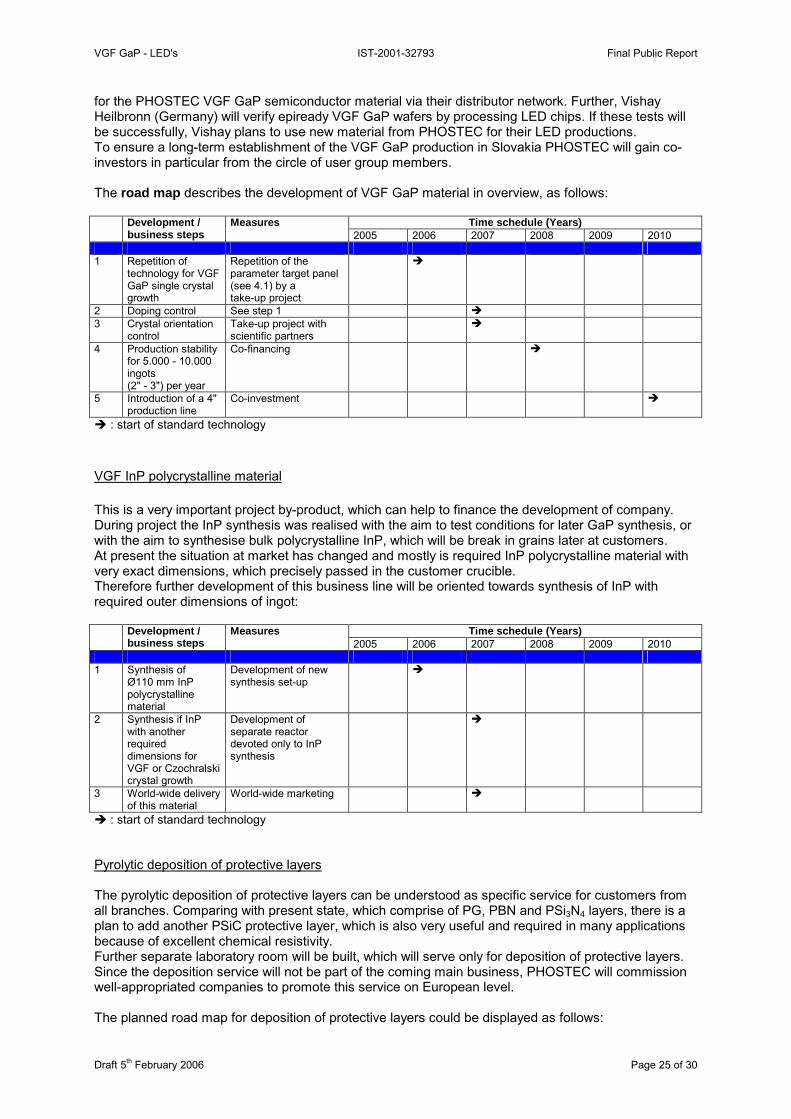
for the PHOSTEC VGF GaP semiconductor material via their distributor network. Further, Vishay Heilbronn (Germany) will verify epiready VGF GaP wafers by processing LED chips. If these tests will be successfully, Vishay plans to use new material from PHOSTEC for their LED productions. To ensure a long-term establishment of the VGF GaP production in Slovakia PHOSTEC will gain co-investors in particular from the circle of user group members. The road map describes the development of VGF GaP material in overview, as follows:
Time schedule (Years) Development / business steps
Measures 2005 2006 2007 2008 2009 2010
1 Repetition of
technology for VGF GaP single crystal growth
Repetition of the parameter target panel (see 4.1) by a take-up project
�
2 Doping control See step 1 � 3 Crystal orientation
control Take-up project with scientific partners
�
4 Production stability for 5.000 - 10.000 ingots (2" - 3") per year
Co-financing �
5 Introduction of a 4" production line
Co-investment �
� : start of standard technology
VGF InP polycrystalline material This is a very important project by-product, which can help to finance the development of company. During project the InP synthesis was realised with the aim to test conditions for later GaP synthesis, or with the aim to synthesise bulk polycrystalline InP, which will be break in grains later at customers. At present the situation at market has changed and mostly is required InP polycrystalline material with very exact dimensions, which precisely passed in the customer crucible. Therefore further development of this business line will be oriented towards synthesis of InP with required outer dimensions of ingot:
Time schedule (Years) Development / business steps
Measures 2005 2006 2007 2008 2009 2010
1 Synthesis of
Ø110 mm InP polycrystalline material
Development of new synthesis set-up
�
2 Synthesis if InP with another required dimensions for VGF or Czochralski crystal growth
Development of separate reactor devoted only to InP synthesis
�
3 World-wide delivery of this material
World-wide marketing �
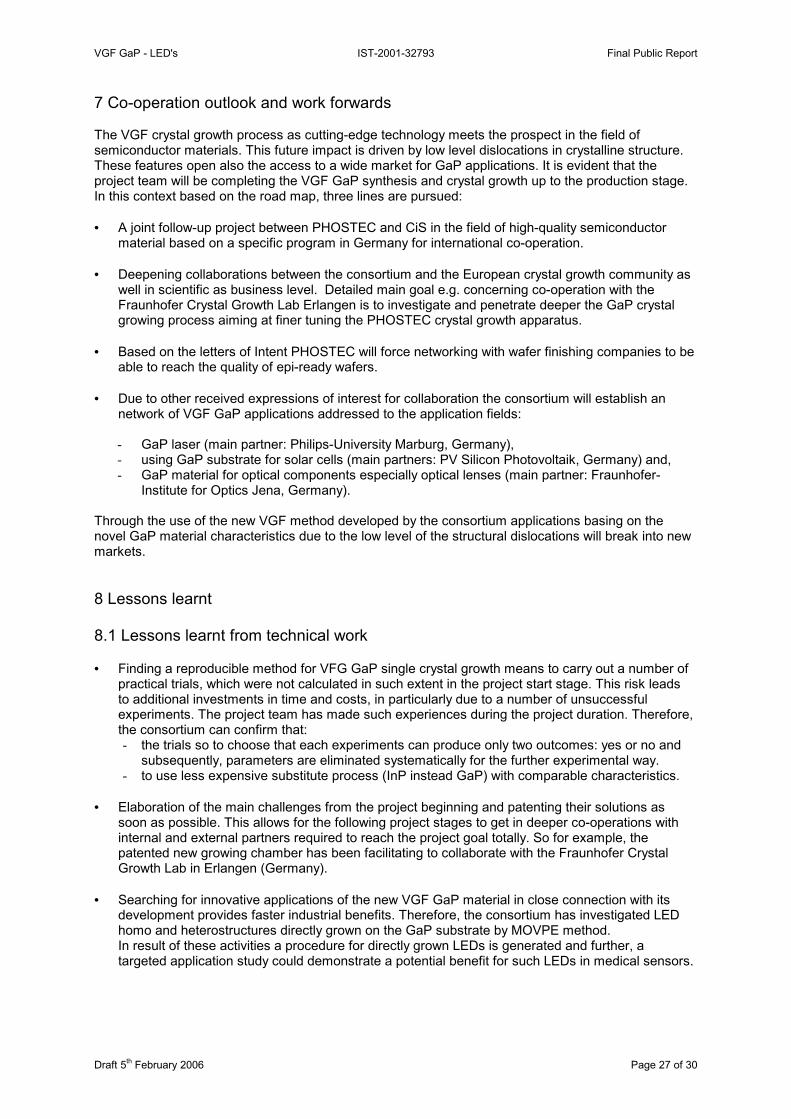
� : start of standard technology Pyrolytic deposition of protective layers The pyrolytic deposition of protective layers can be understood as specific service for customers from all branches. Comparing with present state, which comprise of PG, PBN and PSi3N4 layers, there is a plan to add another PSiC protective layer, which is also very useful and required in many applications because of excellent chemical resistivity. Further separate laboratory room will be built, which will serve only for deposition of protective layers. Since the deposition service will not be part of the coming main business, PHOSTEC will commission well-appropriated companies to promote this service on European level. The planned road map for deposition of protective layers could be displayed as follows:
VGF GaP - LED's IST-2001-32793 Final Public Report
Draft 5th February 2006 Page 26 of 30
Time schedule (Years) Development /
business steps Measures
2005 2006 2007 2008 2009 2010 1 Development of
pyrolytic silicium carbide (PSiC) protective layers
Realisation of series of deposition experiments
�
2 Separate laboratory for deposition of protective layers
Building of laboratory �
3 Delivery of this service to EU market
Tender for commission company
�
� : start of standard technology Directly grown GaP LEDs Up to now, this material is dealt on scientific level and applications are to be opened in the next time. A first application study carried out by CiS has shown that directly grown GaP LEDs may afford improved features for specific applications but deeper investigation are essential. Therefore, next exploitation actions will be focused on feasibility analysis for the directly grown GaP LEDs in different promising application fields in industry and medicine. To evaluate results gaining from these investigations the consortium will use specific portfolio treatments based on two-dimensional consideration of relations between frequency of potential applications and expected benefit. These results will approve a well-founded exploitation of this know-how on scientific level and further, in education and training. For this purpose, FEI STU and SAS will raise laboratory-produced directly grown GaP LEDs and broaden their expertise in this technical field. Expertises in advanced LED structures, MOVPE method and VGF growth processing Exploitation plan on this level would be directed to implement know-how expertise, derived from the results of scientific activities of the Slovak Academy of Sciences and Slovak University of Technology. Their goal will be to design structure for the increased brightness LEDs and to design practical technological manufacturing process. The thing of the exploitation plan will be to transfer developed technology to those EU manufacturing companies, who need this technology for their production processes. It is foreseeable, that this co-operation between Slovakian Scientific Institutions and EU manufactures will lead into important breakthroughs in respected fields of the optoelectronic devices and thus it would forward technological edge of the EU in the global market. There is a specific opening for the implementation of the project results in the field of exploitation of VGF technology for the crystal growth of semiconductor materials. Even though this technology will be developed for the semiconductor GaP material, there is possibility of using the same technology with certain particular adjustments for the growth of other A3B5 semiconductors.
For example we can point to:
- InP material (produced in Europe by Inpact, France) - GaAs material (made in a several places in EU).
To reassert, investigation and a resulting menu will be produced for the transfer of the technologies.
Therefore, it is conceivable that as an added accomplishment of this project will be technological progress in the field of production of relatives of semiconductor materials which are very important for the growth of electronic industry in EU too and by that also important for further expansion of Information Society Technologies.
VGF GaP - LED's IST-2001-32793 Final Public Report
Draft 5th February 2006 Page 27 of 30
7 Co-operation outlook and work forwards The VGF crystal growth process as cutting-edge technology meets the prospect in the field of semiconductor materials. This future impact is driven by low level dislocations in crystalline structure. These features open also the access to a wide market for GaP applications. It is evident that the project team will be completing the VGF GaP synthesis and crystal growth up to the production stage. In this context based on the road map, three lines are pursued: • A joint follow-up project between PHOSTEC and CiS in the field of high-quality semiconductor
material based on a specific program in Germany for international co-operation.
• Deepening collaborations between the consortium and the European crystal growth community as well in scientific as business level. Detailed main goal e.g. concerning co-operation with the Fraunhofer Crystal Growth Lab Erlangen is to investigate and penetrate deeper the GaP crystal growing process aiming at finer tuning the PHOSTEC crystal growth apparatus.
• Based on the letters of Intent PHOSTEC will force networking with wafer finishing companies to be able to reach the quality of epi-ready wafers.
• Due to other received expressions of interest for collaboration the consortium will establish an
network of VGF GaP applications addressed to the application fields: - GaP laser (main partner: Philips-University Marburg, Germany), - using GaP substrate for solar cells (main partners: PV Silicon Photovoltaik, Germany) and, - GaP material for optical components especially optical lenses (main partner: Fraunhofer-
Institute for Optics Jena, Germany). Through the use of the new VGF method developed by the consortium applications basing on the novel GaP material characteristics due to the low level of the structural dislocations will break into new markets. 8 Lessons learnt 8.1 Lessons learnt from technical work • Finding a reproducible method for VFG GaP single crystal growth means to carry out a number of
practical trials, which were not calculated in such extent in the project start stage. This risk leads to additional investments in time and costs, in particularly due to a number of unsuccessful experiments. The project team has made such experiences during the project duration. Therefore, the consortium can confirm that: - the trials so to choose that each experiments can produce only two outcomes: yes or no and
subsequently, parameters are eliminated systematically for the further experimental way. - to use less expensive substitute process (InP instead GaP) with comparable characteristics.
• Elaboration of the main challenges from the project beginning and patenting their solutions as
soon as possible. This allows for the following project stages to get in deeper co-operations with internal and external partners required to reach the project goal totally. So for example, the patented new growing chamber has been facilitating to collaborate with the Fraunhofer Crystal Growth Lab in Erlangen (Germany).
• Searching for innovative applications of the new VGF GaP material in close connection with its
development provides faster industrial benefits. Therefore, the consortium has investigated LED homo and heterostructures directly grown on the GaP substrate by MOVPE method. In result of these activities a procedure for directly grown LEDs is generated and further, a targeted application study could demonstrate a potential benefit for such LEDs in medical sensors.
VGF GaP - LED's IST-2001-32793 Final Public Report
Draft 5th February 2006 Page 28 of 30
8.2 Lesson learnt from dissemination • Starting dissemination activities as early as possible to draw additional benefit for the project
realisation phase. So, the consortium could include information from international experts, like the Industrial Institute of Electronics in Warsaw in early project stages, which are experienced in VGF single crystal growth, but could not solve the VGF GaP synthesis by themselves.
• Comprising all practical results made during the project duration into the dissemination action to
reach a wide target group spectrum and gain benefit from the whole project activities. Following this idea the final report describes all project outcomes being exploitable on the market and for the coming scientific and technical prospects.
• Tailoring the dissemination focus to a balanced relationship between provider's capacity,
investment required to provide and market volume to establish the potential provider as reliable partner for the market. So, niche markets like using VGF GaP for optical components were searched via targeted niche application studies in parallelism to the LED market orientation. As newcomer PHOSTEC will obtain an efficient opportunity to launch the new VGF GaP material to the market.
8.3 Lesson learnt from co-ordination • Because of lot of experiments required to find the right way for VFG GaP crystal growth process
the EU-commission generously allowed a 12 month extension of the project, but nevertheless, the project was side-tracked to the point where VGF GaP substrate was deemed necessary. As result of this process, focus was narrowed into essential subjects necessary for successful completion of the project. Resulting from this experience the focus was tightened, non-essential sub-project were discarded and subsequently, high-quality outcomes were produced. Following the experiences and the recent VGF GaP ingot quality achieved up to now the consortium is sure enough, the parameters for fulfilment of the target panel will be reached within the next half year. Therefore, the project team has decide to continue the co-operation until to the point of completion beyond the official project end too.
• To bring forward the project progress in cost-efficient steps the consortium evaluates that on-site
meetings and partner visits in particular at PHOSTEC proves of value. It was possible, at site growing processes to analyse jointly, failure to identify and measures for improvement jointly to fall. Further, it is true that establishing additional co-operation with external experts leads to additional benefit. In result of the collaboration with the FhG Crystal Growth Lab in Erlangen PHOSTEC was able to distribute the heaters in the new VGF furnace targeted on base on a specific-developed simulation program for optimisation of the temperature field.
• Co-ordination activities have in connection with an early-stage targeted dissemination action
contributed that the consortium could be involved into the European, in particular German Crystal Growth community and the LED community. Both, the crystal developers and the LED substrate applicants will give the project team the guarantee for support in completion of VGF GaP material, industrial testing "epi-ready" wafers and for launching the new VGF GaP material to the market beyond the official project end. Letters of intent given from companies with a strong market position show the above-average industrial interest in VGF GaP substrate.
8.4 Lesson learnt from exploitation The consortium knows that for the project to be extended to complete the development of VGF GaP technology some sort of additional collaboration is needed and efforts toward this end have already been initiated. So, CiS and PHOSTEC have agreed to continue their collaboration via an specific VGF GaP application project to get a better and faster access to the German market.
VGF GaP - LED's IST-2001-32793 Final Public Report
Draft 5th February 2006 Page 29 of 30
References Following references are not explicitly mentioned in the document text, but should give a picture about all work, which was done in the project lifetime. [1] J. Kovac, J. Matuska, J. Novak, D. Starke. Project proposal VGFGaPLEDs, 2002. [2] Kovac. J., Advanced Light Emitting Device Structures for Optoelectronics Applications; Books of
Abstracts, 12th Int. Conf. on thin films, Sept 15-20,2002, Bratislava, Slovakia. [3] Kovac, J. Peternai, L., Lengyel, O., Advanced Light Emitting Device Structures for
Optoelectronics Applications; Thin Solid Films 433 (2003) 22–26. [4] Starke, D., New lighting level for optical measuring tasks, Sensor Report, 2003. [5] Peternai, L., Jakobovic, J., Michalka, M, Ohmic contacts to n - and p-type GaP; Proceedings
APCOM 2003. [6] Kovac, J, Srnanek, R., Peternai, L., Wagner, J., Geurts, J., Irmer, G., Kadlecikova, M.,
Gottschalch, V., Characterisation of GaNP layers by Raman spectroscopy; Proceedings APCOM 2003.
[7] Peternai, L., Jakobovic, J., Kovac, J., Investigations of LED properties with different contacts shapes, EliTech 2003 conference proceedings.
[8] Peternai, L., Jakobovic, J., Kovac, J.,Gottschalch, J., Numerical simulation and analysis of GaP/GaPNP/GaP double heterostructure light-emitting diode, Wocsdice 2004 conference proceedings.
[9] Peternai, L., Jakobovic, J., Kovac, J., Gottschalch, V., Kytka, M., Wrong, T.C., Recent development in LED and OLED technology, Wocsdice 2004 conference proceedings.
[10] Peternai, L., Kováč, J., Jakabovič, J., Gottschalch, V., GaNxP1-x/GaP multiple quantum well structure investigation. APCOM2004 Conference proceedings.
[11] Peternai, L., Computer controlled three dimensional light emission diagram mapping and analyses, COE2004 Conference proceedings.
[12] Kovac, J., Peternai, L., Jakabovic, J., Satka, A., Hasenohrl, S., Novak, J., Gottschalch, V., Rheinlaender, B., New development of LED structures directly grown on GaP substrate, Proceedings of International Conference Electroluminescence 2004, p236-240, Toronto, Sept. 20-23, 2004.
[13] Peternai, L., Kovac, J., Jakabovic, J., Vincze, A., Satka, A, Gottschalch, V., Optical and structural investigation of GaNxP1-x structures for light emitting diodes, 10th JVC Conference proceedings.
[14] Novak, J., Hasenohrl, S., Kovac, J., Peternai, L., Yellow- green quantum well light emitting diodes prepared by MOVPE on transparent substrates, 13th Int. Workshop on Heterostructure Technology, HETECH 2004, Koutolufari, Crete, Sept. 2004, Conference proceedings.
[15] Hasenörl, S., Betko, J., Morvic, M, Novak, J., Fedor, J., Resistivity and mobility in ordered INGaP grown by MOVPE, European Material Research Society 2003 Fall Meeting, 5th Int. Workshop of Molecular Beam Epitaxy and Vapour Phase Growth Physics and Technology, Warsaw 2003.
[16] Novak, J., Hasenörl, S., Alonso, M.I., Garriga, M., Influence of ordered and random parts on properties of InGaP alloy by MOVPE. 10th Int. Workshop on Metal-Organic Vapour Phase Epitaxy - EW MOVPE X. Lecce, Italy 2003.
[17] Novak, J., Kudela, R., Kucera, M., MOVPE growth of AlGaInP quaternary on InGaP pseudosubstrates, 12th Workshop HETECH 03. San Rafael, Spain 2003.
[18] Hasenörl J., Novak J., Vavra I., Material properties of graded composition InxGa1-xP buffer layers grown on GaP by organometallic vapour phase epitaxy, IC-MOVPE 2004, Lahaina, Maui, Hawai (accepted).
[19] Hasenörl J., Novak J., Vavra I, Šatka A., Material properties of graded composition InxGa1-xP buffer layers grown on GaP by organometallic vapour phase epitaxy, J. of Crystal Growht, 272 (2004) 633-641.
[20] Novak, J., Hasenörl, S. Kudela, R., Kucera, M., Growth and characterisation of InxGa1-xP layers with composition close to crossover from direct to indirect band GaP Energy, ICVGE-12 Grenoble, August 2004, J. of Crystal Growth 275/1-2 pp. E1287 - E1292.
[21] Kiċin S, Kromka A, Kudela R, Hasenörl S, Schwarz A and Novak J., Micro-Raman study of InGaP composition grown on V-grooved substrates, Material Science and Engineering B, 113, (2004) 111 - 116.
[22] Leipner, H. S., Structure of imperfect materials. [WWW document]. URL: http://ww.cmat.uni-halle.de/~hsl/Realstruktur/Realstruktur_2_I Growth.pdf. Date: 28.08.2005.
[23] Novák, J., Hasenöhrl, S., Vávra, L., Kučera, M., Spinodal-like Decomposition of InGaP Epitaxial Layers Grown by MOVPE on GaP Substrates; Proc. of EW-MOVPE Lausanne, June 2005.

VGF GaP - LED's IST-2001-32793 Final Public Report
Draft 5th February 2006 Page 30 of 30
[24] Novák, J., Hasenöhrl, S., Vávra, L., OMVPE growth of graded buffer GaP/InxGa1-xP (xIn≥0.27 virtual substrate for optoelectronic applications; Proc. of EW-MOVPE Lausanne, June 2005).
[25] Peternai, L., Kovac, J., Jakabovic, J., Gottschalch, V., Rheinlaender, B., Investigations of GaNxP1-x/GaP LED Structure Optical Properties, Proc. of Electronic Materials Conference 2005, Santa Barbara, USA.
[26] Peternai, L., Kovac, J. Novák, J., Hasenöhrl, S., Satka, S., Vincze, A., Green- orange InGaP LEDs grown on InxGa1-xP/GaP graded buffer substrate, Proc. of Electronic Materials Conference 2005, Santa Barbara, USA.
[27] Novák, J., Hasenöhrl, S., Vávra, L., Kučera, M., Uniformity of epitaxial layers grown on InGaP graded buffers; Proc. of HETECH 05, Bratislava, Slovakia.
[28] Gregušová, D., Novák, J., Hasenöhrl, S., Vávra, L., Kučera, M., Strain and its influence on properties of graded buffers; Proc. of HETECH 05, Bratislava, Slovakia.
[29] Novák, J., Hasenöhrl, S., Vávra, L., Kučera, M., Spinodal-like decomposition of InGaP epitaxial layers grown by MOVPE on GaP substrates; Applied Surface Science, submitted April 2005.
[30] Starke, D., Dissemination and Use Plan. Del. 7.1., 2005. [31] Takac, P., Project website. [WWW document]. URL: http://www.vgfgapleds.sk. Date: 28.08.2005.