Embed Size (px)
Citation preview
IS61/64WV102416EDALL IS61/64WV102416EDBLL
Integrated Silicon Solution, Inc.- www.issi.com 1 Rev. A
11/20/2016
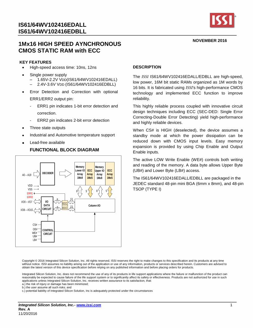
1Mx16 HIGH SPEED AYNCHRONOUS CMOS STATIC RAM with ECC
KEY FEATURES
High-speed access time: 10ns, 12ns
Single power supply – 1.65V-2.2V VDD(IS61/64WV102416EDALL) – 2.4V-3.6V VDD (IS61/64WV102416EDBLL)
Error Detection and Correction with optional
ERR1/ERR2 output pin:
- ERR1 pin indicates 1-bit error detection and
correction.
- ERR2 pin indicates 2-bit error detection
Three state outputs
Industrial and Automotive temperature support
Lead-free available
FUNCTIONAL BLOCK DIAGRAM
COLUMN I/O
WE#UB#
OE#
LB#
CONTROL
CIRCUIT
I/O
DATA
CIRCUIT
DECODER
VDD
VSS
A0 – A19
I/O0 – I/O7
I/O8 – I/O15
Memory
Upper IO
Array
1Mx8
ECC
Array
1Mx5
Column I/O
8 5 8 5
ECC
Array
1Mx5
ECC
ECC
8
8
13
13
Memory
Lower IO
Array
1Mx8
ERR1
ERR2
CS#
DESCRIPTION The ISSI IS61/64WV102416EDALL/EDBLL are high-speed,
low power, 16M bit static RAMs organized as 1M words by
16 bits. It is fabricated using ISSI's high-performance CMOS
technology and implemented ECC function to improve
reliability.
This highly reliable process coupled with innovative circuit
design techniques including ECC (SEC-DED: Single Error
Correcting-Double Error Detecting) yield high-performance
and highly reliable devices.
When CS# is HIGH (deselected), the device assumes a
standby mode at which the power dissipation can be
reduced down with CMOS input levels. Easy memory
expansion is provided by using Chip Enable and Output
Enable inputs.
The active LOW Write Enable (WE#) controls both writing
and reading of the memory. A data byte allows Upper Byte
(UB#) and Lower Byte (LB#) access.
The IS61/64WV102416EDALL/EDBLL are packaged in the
JEDEC standard 48-pin mini BGA (6mm x 8mm), and 48-pin
TSOP (TYPE I)
Copyright © 2016 Integrated Silicon Solution, Inc. All rights reserved. ISSI reserves the right to make changes to this specification and its products at any time without notice. ISSI assumes no liability arising out of the application or use of any information, products or services described herein. Customers are advised to obtain the latest version of this device specification before relying on any published information and before placing orders for products. Integrated Silicon Solution, Inc. does not recommend the use of any of its products in life support applications where the failure or malfunction of the product can reasonably be expected to cause failure of the life support system or to significantly affect its safety or effectiveness. Products are not authorized for use in such applications unless Integrated Silicon Solution, Inc. receives written assurance to its satisfaction, that: a.) the risk of injury or damage has been minimized; b.) the user assume all such risks; and
c.) potential liability of Integrated Silicon Solution, Inc is adequately protected under the circumstances
NOVEMBER 2016

IS61/64WV102416EDALL IS61/64WV102416EDBLL
Integrated Silicon Solution, Inc.- www.issi.com 2 Rev. A
11/20/2016
PIN CONFIGURATIONS 48-Pin mini BGA(6mm x 8mm), A19 on G2 (Package Code : B)
LB# A0OE# A1 A2 NC
I/O8 A3UB# A4 CS# I/O0
I/O9 A5I/O10 A6 I/O1 I/O2
VSS A17I/O11 A7 I/O3 VDD
VDD NCI/O12 A16 I/O4 VSS
I/O14 A14I/O13 A15 I/O5 I/O6
I/O15 A12 A13 WE# I/O7
A18 A9A8 A10 A11
1 2 3 4 5 6
A
B
C
D
E
F
G
H NC
A19
48-Pin mini BGA (6mm x 8mm) , A19 on G2, ERR1/2
(Package Code : B2)
A
B
C
D
E
F
G
H
LB# A0OE# A1 A2 NC
I/O8 A3UB# A4 CS# I/O0
I/O9 A5I/O10 A6 I/O1 I/O2
VSS A17I/O11 A7 I/O3 VDD
VDD ERR1I/O12 A16 I/O4 VSS
I/O14 A14I/O13 A15 I/O5 I/O6
I/O15 A12 A13 WE# I/O7
A18 A9A8 A10 A11 ERR2
1 2 3 4 5 6
A19
48-Pin mini BGA(6mm x 8mm), A19 on H6 (Package Code : B3)
LB# A0OE# A1 A2 NC
I/O8 A3UB# A4 CS# I/O0
I/O9 A5I/O10 A6 I/O1 I/O2
VSS A17I/O11 A7 I/O3 VDD
VDD NCI/O12 A16 I/O4 VSS
I/O14 A14I/O13 A15 I/O5 I/O6
I/O15 A12NC A13 WE# I/O7
A18 A9A8 A10 A11 A19
1 2 3 4 5 6
A
B
C
D
E
F
G
H
48-Pin mini BGA (6mm x 8mm) , A19 on H6, ERR1/2 (Package Code : B4)
A
B
C
D
E
F
G
H
LB# A0OE# A1 A2 NC
I/O8 A3UB# A4 CS# I/O0
I/O9 A5I/O10 A6 I/O1 I/O2
VSS A17I/O11 A7 I/O3 VDD
VDD ERR1I/O12 A16 I/O4 VSS
I/O14 A14I/O13 A15 I/O5 I/O6
I/O15 A12ERR2 A13 WE# I/O7
A18 A9A8 A10 A11 A19
1 2 3 4 5 6

IS61/64WV102416EDALL IS61/64WV102416EDBLL
Integrated Silicon Solution, Inc.- www.issi.com 3 Rev. A
11/20/2016
48-Pin TSOP-I
A2
A1
A0
NC
CS#
I/O0
I/O1
I/O2
I/O3
VDD
VSS
I/O4
I/O5
I/O6
I/O7
WE#
A19
A18
A17
A16
A15
A7
A8
OE#
UB#
LB#
I/O15
I/O14
I/O13
I/O12
VDD
VSS
I/O11
I/O10
I/O9
I/O8
A 9
A10
A11
A12
A13
A14
3
4
5
6
7
8
9
10
11
12
14
13
15
16
17
18
34
33
32
31
30
29
28
27
26
25
23
24
22
21
20
19
44
43
42
41
40
39
38
37
36
35
45
A4
A3
A5
A6
1
2
48
47
46
NC
NC
48-Pin TSOP-I with ERR1/ERR2
A2
A1
A0
ERR1
CS#
I/O0
I/O1
I/O2
I/O3
VDD
VSS
I/O4
I/O5
I/O6
I/O7
WE#
A19
A18
A17
A16
A15
A7
A8
OE#
UB#
LB#
I/O15
I/O14
I/O13
I/O12
VDD
VSS
I/O11
I/O10
I/O9
I/O8
A 9
A10
A11
A12
A13
A14
3
4
5
6
7
8
9
10
11
12
14
13
15
16
17
18
34
33
32
31
30
29
28
27
26
25
23
24
22
21
20
19
44
43
42
41
40
39
38
37
36
35
45
A4
A3
A5
A6
1
2
48
47
46
ERR2
NC
PIN DESCRIPTIONS
A0-A19 Address Inputs
I/O0-I/O15 Data Inputs/Outputs
CS# Chip Enable Input
OE# Output Enable Input
WE# Write Enable Input
LB# Lower-byte Control (I/O0-I/O7)
UB# Upper-byte Control (I/O8-I/O15)
ERR1 1-bit Error Detection and Correction Signal
ERR2 2-bit ERR Detection Signal
NC No Connection
VDD Power
VSS Ground

IS61/64WV102416EDALL IS61/64WV102416EDBLL
Integrated Silicon Solution, Inc.- www.issi.com 4 Rev. A
11/20/2016
FUNCTION DESCRIPTION SRAM is one of random access memories. Each byte or word has an address and can be accessed randomly. SRAM has three different modes supported. Each function is described below with Truth Table.
STANDBY MODE Device enters standby mode when deselected (CS# HIGH). The input and output pins (I/O0-15) are placed in a high impedance state. CMOS input in this mode will maximize saving power.
WRITE MODE Write operation issues with Chip selected (CS#) and Write Enable (WE#) input LOW. The input and output pins (I/O0-15) are in data input mode. Output buffers are closed during this time even if OE# is LOW. UB# and LB# enables a byte write feature. By enabling LB# LOW, data from I/O pins (I/O0 through I/O7) are written into the location specified on the address pins. And with UB# being LOW, data from I/O pins (I/O8 through I/O15) are written into the location.
READ MODE Read operation issues with Chip selected (CS# LOW) and Write Enable (WE#) input HIGH. When OE# is LOW, output buffer turns on to make data output. Any input to I/O pins during READ mode is not permitted. UB# and LB# enables a byte read feature. By enabling LB# LOW, data from memory appears on I/O0-7. And with UB# being LOW, data from memory appears on I/O8-15. In the READ mode, output buffers can be turned off by pulling OE# HIGH. In this mode, internal device operates as READ but I/Os are in a high impedance state. Since device is in READ mode, active current is used. ERROR DETECTION AND ERROR CORRECTION
Independent ECC per each byte
- detect and correct one bit error per byte or detect 2-bit error per byte Optional ERR1 output signal indicates 1-bit error detection and correction
Optional ERR2 output signal indicates 2-bit error detection.
Controller can use either ERR1 or ERR2 to monitor ECC event. Unused pins (ERR1 or ERR2) can be left floating.
Better reliability than parity code schemes which can only detect an error but not correct an error
Backward Compatible: Drop in replacement to current in industry standard devices (without ECC)
ERR1, ERR2 OUTPUT SIGNAL BEHAVIOR
ERR1 ERR2 DQ pin Status Remark
0 0 Valid Q No Error
1 0 Valid Q 1-Bit Error only 1-bit error per byte detected and corrected
0 1 In-Valid Q 2-Bit Error only No 1-bit error. 2-bit error per byte detected (out of 2 bytes)
1 1 In-Valid Q 1-bit & 2-bit error 1-bit error detected and corrected at one byte, and 2-bit error detected at another byte.
High-Z High-Z Valid D Non-Read Write operation or Output Disabled

IS61/64WV102416EDALL IS61/64WV102416EDBLL
Integrated Silicon Solution, Inc.- www.issi.com 5 Rev. A
11/20/2016
TRUTH TABLE
Mode CS# WE# OE# LB# UB# I/O0-I/O7 I/O8-I/O15 VDD Current
Not Selected H X X X X High-Z High-Z ISB1, ISB2
Output Disabled L H H L L High-Z High-Z
ICC L H H H L High-Z High-Z
Read
L H L L H DOUT High-Z
ICC L H L H L High-Z DOUT
L H L L L DOUT DOUT
Write
L L X L H DIN High-Z
ICC L L X H L High-Z DIN
L L X L L DIN DIN
POWER UP INITIALIZATION The device includes on-chip voltage sensor used to launch POWER-UP initialization process. When VDD reaches stable level, the device requires 150us of tPU (Power-Up Time) to complete its self-initialization process. When initialization is complete, the device is ready for normal operation.
tPU 150 us
VDD
Stable VDD
0VDevice Initialization Device for Normal Operation

IS61/64WV102416EDALL IS61/64WV102416EDBLL
Integrated Silicon Solution, Inc.- www.issi.com 6 Rev. A
11/20/2016
ABSOLUTE MAXIMUM RATINGS AND OPERATING RANGE
ABSOLUTE MAXIMUM RATINGS(1) Symbol Parameter Value Unit
Vterm Terminal Voltage with Respect to VSS –0.5 to VDD + 0.5V V
VDD VDD Related to VSS –0.3 to 4.0 V
tStg Storage Temperature –65 to +150 C
PT Power Dissipation 1.0 W
Note:
1. Stress greater than those listed under ABSOLUTE MAXIMUM RATINGS may cause permanent damage to the device. This is a stress rating only and functional operation of the device at these or any other conditions above those indicated in the operational sections of this specification is not implied. Exposure to absolute maximum rating conditions for extended periods may affect reliability.
.
PIN CAPACITANCE (1) Parameter Symbol Test Condition Max Units
Input capacitance CIN TA = 25°C, f = 1 MHz, VDD = VDD(typ)
6 pF
DQ capacitance (IO0–IO15) CI/O 8 pF
Note: 1. These parameters are guaranteed by design and tested by a sample basis only.
OPERATING RANGE(1)
Range Ambient Temperature
PART NUMBER VDD SPEED (MAX)
Commercial 0C to +70C IS61WV102416EDALL 1.65V – 2.2V
10 ns IS61WV102416EDBLL 2.4V – 3.6V
Industrial -40C to +85C IS61WV102416EDALL 1.65V – 2.2V
10 ns IS61WV102416EDBLL 2.4V – 3.6V
Automotive (A3) -40C to +125C IS64WV102416EDALL 1.65V – 2.2V
12 ns IS64WV102416EDBLL 2.4V – 3.6V

IS61/64WV102416EDALL IS61/64WV102416EDBLL
Integrated Silicon Solution, Inc.- www.issi.com 7 Rev. A
11/20/2016
AC TEST CONDITIONS (OVER THE OPERATING RANGE)
Parameter Unit (1.65V~2.2V)
Unit (2.4V~3.6V)
Input Pulse Level 0V to VDD 0V to VDD
Input Rise and Fall Time 1.5 ns 1.5 ns
Output Timing Reference Level ½ VDD ½ VDD
R1 (ohm) 13500 319
R2 (ohm) 10800 353
VTM (V) 1.8V 3.3V
Output Load Conditions Refer to Figure 1 and 2
AC TEST LOADS
Output
Zo = 50 ohm50 ohm
30 pF,
Including
jig
and scope
VDD/2
R1
R2
VTM
OUTPUT5pF,
Including
jig
and scope
R1
R2
VTM
OUTPUT5pF,
Including
jig
and scope
FIGURE 1 FIGURE 2

IS61/64WV102416EDALL IS61/64WV102416EDBLL
Integrated Silicon Solution, Inc.- www.issi.com 8 Rev. A
11/20/2016
DC ELECTRICAL CHARACTERISTICS
DC ELECTRICAL CHARACTERISTICS (OVER THE OPERATING RANGE)
VDD = 1.65V – 2.2V
Symbol Parameter Test Conditions Min. Max. Unit
VOH Output HIGH Voltage IOH = -0.1 mA 1.4 — V
VOL Output LOW Voltage IOL = 0.1 mA — 0.2 V
VIH(1) Input HIGH Voltage 1.4 VDD + 0.2 V
VIL(1) Input LOW Voltage –0.2 0.4 V
ILI Input Leakage GND < VIN < VDD –1 1 µA
ILO Output Leakage GND < VIN < VDD, Output Disabled –1 1 µA
Note: 1. VILL(min) = -1.0V AC (pulse width < 10ns). Not 100% tested. VIHH (max) = VDD + 1.0V AC (pulse width < 10ns). Not 100% tested.
VDD = 2.4V – 3.6V
Symbol Parameter Test Conditions Min. Max. Unit
VOH Output HIGH Voltage
2.4V ~ 2.7V VDD = Min., IOH = -1.0 mA 2.0 —
V
2.7V ~ 3.6V VDD = Min., IOH = -4.0 mA 2.2
VOL Output LOW Voltage
2.4V ~ 2.7V VDD = Min., IOL = 2.0 mA — 0.4 V
2.7V ~ 3.6V VDD = Min., IOL = 8.0 mA — 0.4
VIH(1) Input HIGH Voltage 2.4V ~ 2.7V 2.0
VDD + 0.3 V
2.7V ~ 3.6V 2.0
VIL(1) Input LOW Voltage 2.4V ~ 2.7V –0.3 0.6 V
2.7V ~ 3.6V –0.3 0.8
ILI Input Leakage VSS < VIN < VDD –2 2 µA
ILO Output Leakage VSS < VIN < VDD, Output Disabled –2 2 µA
Note: 1. VIL(min) = -0.3V DC ; VIL(min) = -2.0V AC (pulse width 2.0ns). Not 100% tested. VIH (max) = VDD + 0.3V DC ; VIH(max) = VDD + 2.0V AC (pulse width 2.0ns). Not 100% tested.

IS61/64WV102416EDALL IS61/64WV102416EDBLL
Integrated Silicon Solution, Inc.- www.issi.com 9 Rev. A
11/20/2016
POWER SUPPLY CHARACTERISTICS-II FOR POWER (OVER THE OPERATING RANGE)
Symbol Parameter Test Conditions Grade -10
Max. -12
Max. Unit
ICC VDD Dynamic Operating
Supply Current VDD = MAX, IOU T = 0 mA, f = fMAX
Com. 90 85
mA Ind. 100 95
Auto. 140 135
ICC1 Operating Supply Current VDD = MAX, IOUT = 0 mA, f = 0
Com. 80 80
mA Ind. 90 90
Auto. 110 110
ISB1 TTL Standby Current
(TTL Inputs)
VDD = MAX, VIN = VIH or VIL
CS# ≥ VIH , f = 0
Com. 60 60
mA Ind. 70 70
Auto. 110 110
ISB2 CMOS Standby Current
(CMOS Inputs)
VDD = MAX,
CS# ≥ VDD - 0.2V
VIN ≥ VDD - 0.2V , or VIN ≤ 0.2V
, f = 0
Com. 50 50
mA Ind. 60 60
Auto. 100 100
Typ. (2) 10
Notes:
1. At f = fMAX, address and data inputs are cycling at the maximum frequency, f = 0 means no input line change. 2. Typical values are measured at VDD = 3.0V/1.8V, TA = 25 °C and not 100% tested.

IS61/64WV102416EDALL IS61/64WV102416EDBLL
Integrated Silicon Solution, Inc.- www.issi.com 10 Rev. A
11/20/2016
AC CHARACTERISTICS (OVER OPERATING RANGE)
READ CYCLE AC CHARACTERISTICS
Parameter Symbol -10(1) -12(1)
unit notes Min Min Min Max
Read Cycle Time tRC 10 - 12 - ns
Address Access Time tAA - 10 - 12 ns
Output Hold Time tOHA 2.5 - 2.5 - ns
CS# Access Time tACE - 10 - 12 ns
OE# Access Time tDOE - 6 - 7 ns
OE# to High-Z Output tHZOE 0 5 0 6 ns 2
OE# to Low-Z Output tLZOE 0 - 0 - ns 2
CS# to High-Z Output tHZCE 0 5 0 6 ns 2
CS# to Low-Z Output tLZCE 3 - 3 - ns 2
UB#, LB# Access Time tBA - 6 - 7 ns
UB#, LB# to High-Z Output tHZB 0 5 0 6 ns 2
UB#, LB# to Low-Z Output tLZB 0 - 0 - ns 2 Notes:
1. Test conditions assume signal transition times of 1.5 ns or less, timing reference levels of VDD/2, input pulse levels of 0V to VDD and output loading specified in Figure 1.
2. Tested with the load in Figure 2. Transition is measured ±500 mV from steady-state voltage. Not 100% tested.
AC WAVEFORMS
READ CYCLE NO. 1(1,2) (ADDRESS CONTROLLED, CS# = OE# = UB# = LB# = LOW, WE# = HIGH)
tRC
Address
DQ 0-15
tOHA tOHA
tAA
PREVIOUS DATA VALID DATA VALID
PREVIOUS ERROR VALID ERROR1 VALIDERR1
LOW-Z
LOW-Z
PREVIOUS ERROR VALID ERROR2 VALIDERR2 LOW-Z
Notes: 1. The device is continuously selected. 2. ERR1, ERR2 signals act like a Read Data Q during Read Operation.

IS61/64WV102416EDALL IS61/64WV102416EDBLL
Integrated Silicon Solution, Inc.- www.issi.com 11 Rev. A
11/20/2016
READ CYCLE NO. 2(1) (OE# CONTROLLED, WE# = HIGH)
OE#
CS#
DOUT
tAA
ADDRESS
tRC
tOHA
tDOE
tLZOE
tACS
tLZCS
tHZOE
tHZCS
HIGH-ZDATA VALID
tLZB
tHZBtBA
UB#,LB#
LOW-Z
Note: 1. Address is valid prior to or coincident with CS# LOW transition.

IS61/64WV102416EDALL IS61/64WV102416EDBLL
Integrated Silicon Solution, Inc.- www.issi.com 12 Rev. A
11/20/2016
WRITE CYCLE AC CHARACTERISTICS
Parameter Symbol -10(1) -12(1)
unit notes Min Max Min Max
Write Cycle Time tWC 10 - 12 - ns
CS# to Write End tSCS 8 - 9 - ns
Address Setup Time to Write End tAW 8 - 9 - ns
UB#,LB# to Write End tPWB 8 - 9 - ns
Address Hold from Write End tHA 0 - 0 - ns
Address Setup Time tSA 0 - 0 - ns
WE# Pulse Width tPWE1 8 - 9 - ns
WE# Pulse Width (OE# = LOW) tPWE2 10 - 12 - ns 2
Data Setup to Write End tSD 6 - 7 - ns
Data Hold from Write End tHD 0 - 0 - ns
WE# LOW to High-Z Output tHZWE - 4 - 5 ns
WE# HIGH to Low-Z Output tLZWE 2 - 2 - ns Notes:
1 The internal write time is defined by the overlap of CS# = LOW, UB# or LB# = LOW, and WE# = LOW. All conditions must be in valid states to initiate a Write, but any condition can go inactive to terminate the Write. The Data Input Setup and Hold timing are referenced to the rising or falling edge of the signal that terminates the write.
2 tPWE > tHZWE + tSD when OE# is LOW.
AC WAVEFORMS
WRITE CYCLE NO. 1 (CS# CONTROLLED, OE# = HIGH OR LOW)
ADDRESS
CS#
WE#
UB#,LB#
DOUT
DIN
tWC
tHA
tAW
tPWE
tPWB
tSA
tHZWEtLZWE
tSD tHD
DATA IN VALID
DATA UNDEFINEDHIGH-Z
DATA UNDEFINED
tSCS
(1)
(2)
Note:
1. tHZWE is based on the assumption when tSA=0nS after READ operation. Actual DOUT for tHZWE may not appear if OE# goes high before Write Cycle.

IS61/64WV102416EDALL IS61/64WV102416EDBLL
Integrated Silicon Solution, Inc.- www.issi.com 13 Rev. A
11/20/2016
WRITE CYCLE NO. 2(1,2) (WE# CONTROLLED: OE# IS HIGH DURING WRITE CYCLE)
ADDRESS
CS#
WE#
UB#,LB#
DOUT
DIN
tWC
tHA
tAW
tPWE
tPWB
tSA
tHZOE
tSD tHD
DATA IN VALID
DATA UNDEFINEDHIGH-Z
DATA UNDEFINED
tSCS
(1)
(2)
OE#
Notes: 1. tHZOE is the time DOUT goes to High-Z after OE# goes high. 2. During this period the I/Os are in output state. Do not apply input signals.
WRITE CYCLE NO. 3(1) (WE# CONTROLLED: OE# IS LOW DURING WRITE CYCLE)
tWC
tHAtAW
tPWE2
tSA
tHZWE tLZWEHIGHZ
tSD tHD
DATA UNDEFINED
DATA IN VALID
ADDRESS
CS#=LOW
WE#
DOUT
DIN
OE# = LOW
tPWBUB#,LB#
Note: 1. If OE# is low during write cycle, tHZWE must be met in the application. Do not apply input signal during this period. Data output from the
previous READ operation will drive IO BUS.
IS61/64WV102416EDALL IS61/64WV102416EDBLL
Integrated Silicon Solution, Inc.- www.issi.com 14 Rev. A
11/20/2016
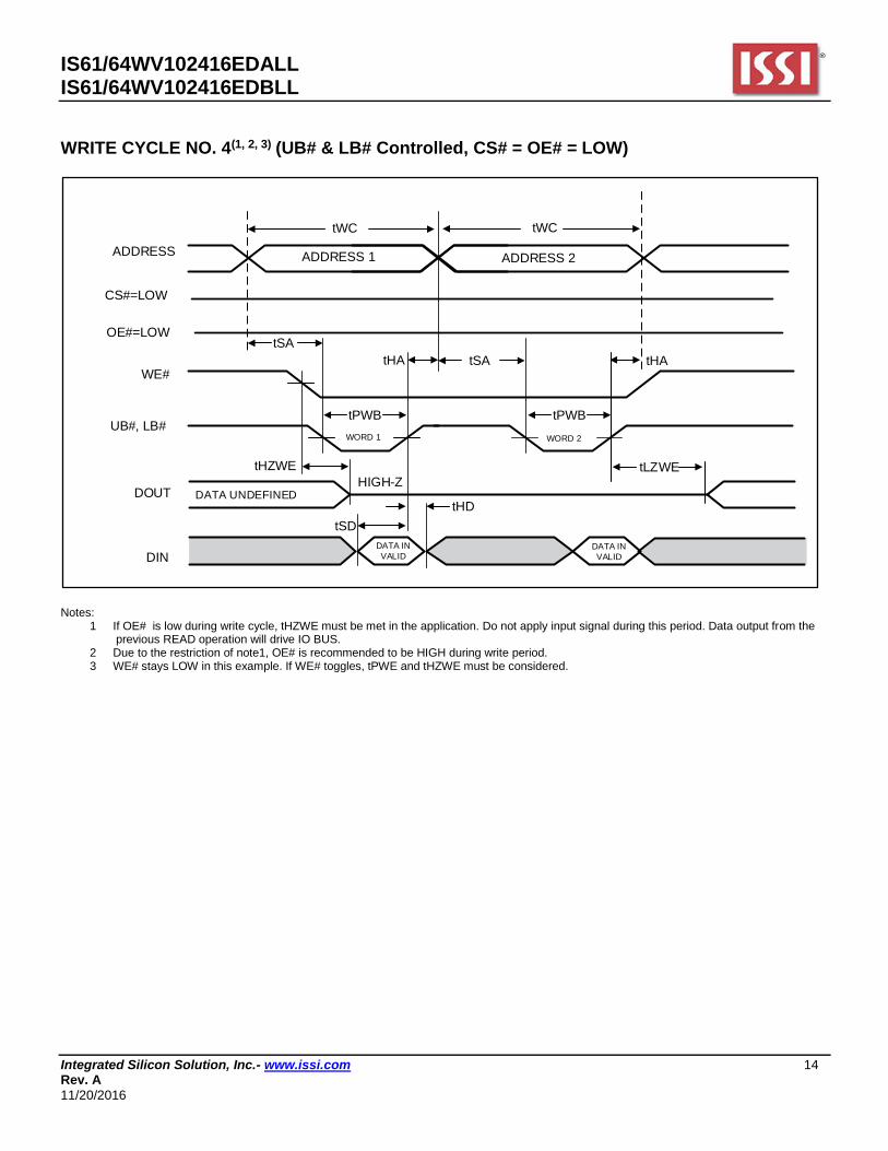
WRITE CYCLE NO. 4(1, 2, 3) (UB# & LB# Controlled, CS# = OE# = LOW)
ADDRESS
WE#
DOUT
DIN
tSA
tHZWE
tPWB
tHA
DATA IN
VALID
ADDRESS 1 ADDRESS 2
tWC
DATA IN
VALID
DATA UNDEFINEDtHD
tSD
HIGH-ZtLZWE
WORD 1 WORD 2
UB#, LB#
tHA
OE#=LOW
CS#=LOW
tSA
tPWB
tWC
Notes:
1 If OE# is low during write cycle, tHZWE must be met in the application. Do not apply input signal during this period. Data output from the previous READ operation will drive IO BUS.
2 Due to the restriction of note1, OE# is recommended to be HIGH during write period. 3 WE# stays LOW in this example. If WE# toggles, tPWE and tHZWE must be considered.

IS61/64WV102416EDALL IS61/64WV102416EDBLL
Integrated Silicon Solution, Inc.- www.issi.com 15 Rev. A
11/20/2016
DATA RETENTION CHARACTERISTICS
Symbol Parameter Test Condition OPTION Min. Typ.(2) Max. Unit
VDR VDD for Data
Retention See Data Retention Waveform
VDD = 2.4V to 3.6V 2.0 3.6
V
VDD = 1.65V to 2.2V 1.2 3.6
IDR Data Retention
Current VDD= VDR(min), CS# ≥ VDD – 0.2V
Com. - 10 50
mA Ind. - - 60
Auto - - 100
tSDR Data Retention
Setup Time See Data Retention Waveform
0 - - ns
tRDR Recovery Time See Data Retention Waveform tRC - - ns
Notes:
1. If CS# > VDD–0.2V, all other inputs including UB# and LB# must meet this condition. 2. Typical values are measured at VDD = VDR (Min), TA = 25 °C and not 100% tested.
DATA RETENTION WAVEFORM (CS# CONTROLLED)
GND
CS#
VDR
VDD
CS# > VDD – 0.2V
Data Retention ModetSDR tRDR

IS61/64WV102416EDALL IS61/64WV102416EDBLL
Integrated Silicon Solution, Inc.- www.issi.com 16 Rev. A
11/20/2016
ORDERING INFORMATION
Commercial Range: 0°C to +70°C, Voltage Range: 2.4V to 3.6V
Speed (ns) Order Part No. Package
10 IS61WV102416EDBLL-10B mini BGA (6mm x 8mm)
10 IS61WV102416EDBLL-10BL mini BGA (6mm x 8mm), Lead-free
10 IS61WV102416EDBLL-10B2 mini BGA (6mm x 8mm), ERR1/ERR2 Pins
10 IS61WV102416EDBLL-10B2L mini BGA (6mm x 8mm), ERR1/ERR2 Pins, Lead-free
10 IS61WV102416EDBLL-10TL TSOP (Type I) , Lead-free
10 IS61WV102416EDBLL-10T2L TSOP (Type I), ERR1/ERR2 Pins , Lead-free
Industrial Range: -40°C to +85°C, Voltage Range: 1.65V to 2.2V
Speed (ns) Order Part No. Package
10 IS61WV102416EDALL-10BI mini BGA (6mm x 8mm)
10 IS61WV102416EDALL-10BLI mini BGA (6mm x 8mm), Lead-free
10 IS61WV102416EDALL-10B2I mini BGA (6mm x 8mm), ERR1/ERR2 Pins
10 IS61WV102416EDALL-10B2LI mini BGA (6mm x 8mm), ERR1/ERR2 Pins, Lead-free
10 IS61WV102416EDALL-10TLI TSOP (Type I) , Lead-free
10 IS61WV102416EDALL-10T2LI TSOP (Type I), ERR1/ERR2 Pins , Lead-free
Industrial Range: -40°C to +85°C, Voltage Range: 2.4V to 3.6V
Speed (ns) Order Part No. Package
10 IS61WV102416EDBLL-10BI mini BGA (6mm x 8mm)
10 IS61WV102416EDBLL-10BLI mini BGA (6mm x 8mm), Lead-free
10 IS61WV102416EDBLL-10B2I mini BGA (6mm x 8mm), ERR1/ERR2 Pins
10 IS61WV102416EDBLL-10B2LI mini BGA (6mm x 8mm), ERR1/ERR2 Pins, Lead-free
10 IS61WV102416EDBLL-10TLI TSOP (Type I) , Lead-free
10 IS61WV102416EDBLL-10T2LI TSOP (Type I), ERR1/ERR2 Pins , Lead-free
*Contact ISSI MKT for B3/B4 (A19 on H6) BGA Packages.

IS61/64WV102416EDALL IS61/64WV102416EDBLL
Integrated Silicon Solution, Inc.- www.issi.com 17 Rev. A
11/20/2016
Automotive (A3) Range: –40°C to +125°C, Voltage Range: 1.65V to 2.2V
Speed (ns) Order Part No. Package
12 IS64WV102416EDALL-12BA3 mini BGA (6mm x 8mm)
12 IS64WV102416EDALL-12BLA3 mini BGA (6mm x 8mm), Lead-free
12 IS64WV102416EDALL-12B2A3 mini BGA (6mm x 8mm), ERR1/ERR2 Pins
12 IS64WV102416EDALL-12B2LA3 mini BGA (6mm x 8mm), ERR1/ERR2 Pins, Lead-free
12 IS64WV102416EDALL-12CTLA3 TSOP (Type I), Copper Leadframe, Lead-free
12 IS64WV102416EDALL-12CT2LA3 TSOP (Type I), ERR1/ERR2 Pins, Copper Leadframe, Lead-free
Automotive (A3) Range: –40°C to +125°C, Voltage Range: 2.4V to 3.6V
Speed (ns) Order Part No. Package
12 IS64WV102416EDBLL-12BA3 mini BGA (6mm x 8mm)
12 IS64WV102416EDBLL-12BLA3 mini BGA (6mm x 8mm), Lead-free
12 IS64WV102416EDBLL-12B2A3 mini BGA (6mm x 8mm), ERR1/ERR2 Pins
12 IS64WV102416EDBLL-12B2LA3 mini BGA (6mm x 8mm), ERR1/ERR2 Pins, Lead-free
12 IS64WV102416EDBLL-12CTLA3 TSOP (Type I), Copper Leadframe, Lead-free
12 IS64WV102416EDBLL-12CT2LA3 TSOP (Type I), ERR1/ERR2 Pins, Copper Leadframe, Lead-free
*Contact ISSI MKT for B3/B4 (A19 on H6) BGA Packages.

IS61/64WV102416EDALL IS61/64WV102416EDBLL
Integrated Silicon Solution, Inc.- www.issi.com 18 Rev. A
11/20/2016
PACKAGE INFORMATION

IS61/64WV102416EDALL IS61/64WV102416EDBLL
Integrated Silicon Solution, Inc.- www.issi.com 19 Rev. A
11/20/2016