Embed Size (px)
Citation preview
2027
Pure Appl. Chem., Vol. 82, No. 11, pp. 2027–2053, 2010.doi:10.1351/PAC-CON-09-09-18© 2010 IUPAC, Publication date (Web): 6 August 2010
Vapor-phase synthesis of one-dimensional ZnS,CdS, and ZnxCd1–xS nanostructures*
Tianyou Zhai‡, Xiaosheng Fang‡, Haibo Zeng, Xijin Xu‡,Yoshio Bando, and Dmitri Golberg
International Center for Young Scientists (ICYS) and International Center forMaterials Nanoarchitectonics (MANA), National Institute for Materials Science(NIMS), Namiki 1-1, Tsukuba, Ibaraki 305-0044, Japan
Abstract: One-dimensional (1D) nanostructures have received prime attention due to theirhigh potential in understanding fundamental physical concepts and constructing nanoscaleelectronic devices. ZnS and CdS, the well-known direct and wide bandgap semiconductors,have recently attracted significant research interest due to their special properties and appli-cations in sensing, optoelectronics, piezoelectronics, and lasing. This article reviews the mostrecent activities in ZnS and CdS nanostructures, with an emphasis on the authors’ own re-sults, and on 1D ZnS and CdS nanostructures, especially those synthesized using vapor dep-osition techniques. The review begins with a survey of ZnS and CdS nanostructures, and thenis primarily focused on their 1D nanostructures, syntheses, characterizations, formationmechanisms, and optical and field-emission (FE) properties. Additionally, developments ofZnxCd1–xS composite nanostructures, including nanocombs and zigzag nanowires, are alsodiscussed. Finally, we conclude this review with the perspectives and outlook on the futuredevelopments in this field.
Keywords: CdS; nanomaterials; nanostructures; vapor-phase synthesis; ZnS.
INTRODUCTION
One-dimensional (1D) nanostructures such as nanowires, nanobelts, nanotubes, and nanorods havestimulated an increasing interest due to their importance in basic scientific research and potential tech-nological applications [1–3]. It is generally accepted that 1D nanostructures are ideal systems for ex-ploring a large number of novel phenomena at the nanoscale and investigating the size and dimension-ality dependence of functional properties [4]. They are also expected to play important roles as bothinterconnects and the key units in fabricating electronic, optoelectronic, electrochemical, and electro-mechanical devices with nanoscale dimensions [5]. As important II–VI semiconductors, ZnS and CdSare some of the first semiconductors discovered and probably some of the most important electronic andoptoelectronic materials with prominent applications in nonlinear optical devices, flat panel displays,light-emitting diodes, laser, logic gates, transistors, etc. [6,7].
It is evident that the research on 1D ZnO nanostructures has rapidly expanded in recent years be-cause of their special structures and novel properties. As pointed out by Zhong Lin Wang in one of thelatest reviews, 1D ZnO has been one of the few dominant nanomaterials in nanotechnology along with
*Paper based on a presentation at the 5th International Symposium on Novel Materials and Their Synthesis (NMS-V) and the19th International Symposium on Fine Chemistry and Functional Polymers (FCFP-XIX), 18–22 October 2009, Shanghai, China.Other presentations are published in this issue, pp. 1975–2229.‡Corresponding authors: E-mail: [email protected] or [email protected] (T. Y. Zhai), [email protected](X. S. Fang), [email protected] (X. J. Xu); Fax: 81-29-851-6280
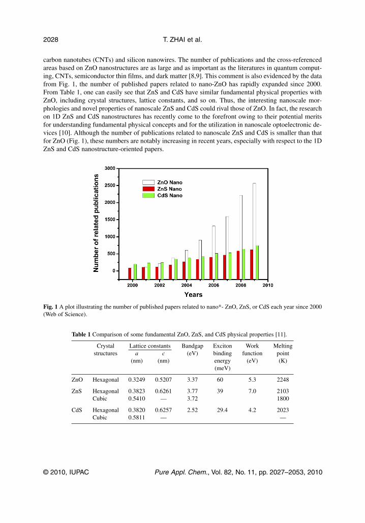
carbon nanotubes (CNTs) and silicon nanowires. The number of publications and the cross-referencedareas based on ZnO nanostructures are as large and as important as the literatures in quantum comput-ing, CNTs, semiconductor thin films, and dark matter [8,9]. This comment is also evidenced by the datafrom Fig. 1, the number of published papers related to nano-ZnO has rapidly expanded since 2000.From Table 1, one can easily see that ZnS and CdS have similar fundamental physical properties withZnO, including crystal structures, lattice constants, and so on. Thus, the interesting nanoscale mor-phologies and novel properties of nanoscale ZnS and CdS could rival those of ZnO. In fact, the researchon 1D ZnS and CdS nanostructures has recently come to the forefront owing to their potential meritsfor understanding fundamental physical concepts and for the utilization in nanoscale optoelectronic de-vices [10]. Although the number of publications related to nanoscale ZnS and CdS is smaller than thatfor ZnO (Fig. 1), these numbers are notably increasing in recent years, especially with respect to the 1DZnS and CdS nanostructure-oriented papers.
Table 1 Comparison of some fundamental ZnO, ZnS, and CdS physical properties [11].
Crystal Lattice constants Bandgap Exciton Work Meltingstructures a c (eV) binding function point
(nm) (nm) energy (eV) (K)(meV)
ZnO Hexagonal 0.3249 0.5207 3.37 60 5.3 2248
ZnS Hexagonal 0.3823 0.6261 3.77 39 7.0 2103Cubic 0.5410 — 3.72 1800
CdS Hexagonal 0.3820 0.6257 2.52 29.4 4.2 2023Cubic 0.5811 — —
T. ZHAI et al.
© 2010, IUPAC Pure Appl. Chem., Vol. 82, No. 11, pp. 2027–2053, 2010
2028
Fig. 1 A plot illustrating the number of published papers related to nano*- ZnO, ZnS, or CdS each year since 2000(Web of Science).
This article reviews the most recent research activities in ZnS and CdS nanostructures, with anemphasis on the authors’ own results, and on 1D ZnS and CdS nanostructures, especially on those syn-thesized using vapor depositions.
CRYSTALLOGRAPHIC STRUCTURE OF ZnS AND CdS
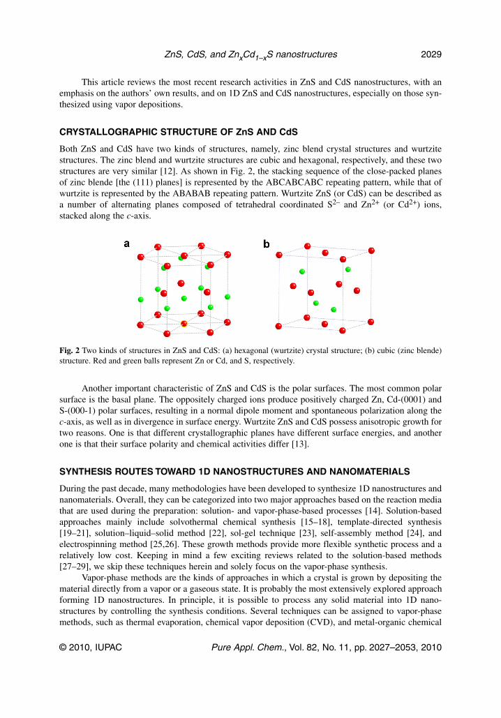
Both ZnS and CdS have two kinds of structures, namely, zinc blend crystal structures and wurtzitestructures. The zinc blend and wurtzite structures are cubic and hexagonal, respectively, and these twostructures are very similar [12]. As shown in Fig. 2, the stacking sequence of the close-packed planesof zinc blende [the (111) planes] is represented by the ABCABCABC repeating pattern, while that ofwurtzite is represented by the ABABAB repeating pattern. Wurtzite ZnS (or CdS) can be described asa number of alternating planes composed of tetrahedral coordinated S2– and Zn2+ (or Cd2+) ions,stacked along the c-axis.
Another important characteristic of ZnS and CdS is the polar surfaces. The most common polarsurface is the basal plane. The oppositely charged ions produce positively charged Zn, Cd-(0001) andS-(000-1) polar surfaces, resulting in a normal dipole moment and spontaneous polarization along thec-axis, as well as in divergence in surface energy. Wurtzite ZnS and CdS possess anisotropic growth fortwo reasons. One is that different crystallographic planes have different surface energies, and anotherone is that their surface polarity and chemical activities differ [13].
SYNTHESIS ROUTES TOWARD 1D NANOSTRUCTURES AND NANOMATERIALS
During the past decade, many methodologies have been developed to synthesize 1D nanostructures andnanomaterials. Overall, they can be categorized into two major approaches based on the reaction mediathat are used during the preparation: solution- and vapor-phase-based processes [14]. Solution-basedapproaches mainly include solvothermal chemical synthesis [15–18], template-directed synthesis[19–21], solution–liquid–solid method [22], sol-gel technique [23], self-assembly method [24], andelectrospinning method [25,26]. These growth methods provide more flexible synthetic process and arelatively low cost. Keeping in mind a few exciting reviews related to the solution-based methods[27–29], we skip these techniques herein and solely focus on the vapor-phase synthesis.
Vapor-phase methods are the kinds of approaches in which a crystal is grown by depositing thematerial directly from a vapor or a gaseous state. It is probably the most extensively explored approachforming 1D nanostructures. In principle, it is possible to process any solid material into 1D nano -structures by controlling the synthesis conditions. Several techniques can be assigned to vapor-phasemethods, such as thermal evaporation, chemical vapor deposition (CVD), and metal-organic chemical
© 2010, IUPAC Pure Appl. Chem., Vol. 82, No. 11, pp. 2027–2053, 2010
ZnS, CdS, and ZnxCd1–xS nanostructures 2029
Fig. 2 Two kinds of structures in ZnS and CdS: (a) hexagonal (wurtzite) crystal structure; (b) cubic (zinc blende)structure. Red and green balls represent Zn or Cd, and S, respectively.
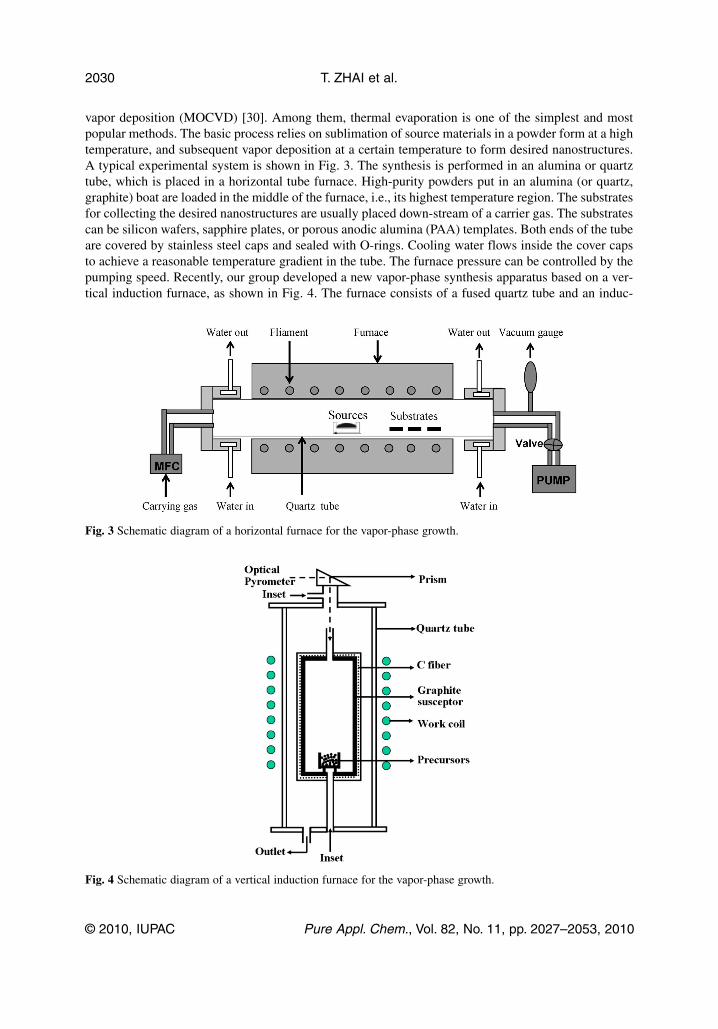
vapor deposition (MOCVD) [30]. Among them, thermal evaporation is one of the simplest and mostpopular methods. The basic process relies on sublimation of source materials in a powder form at a hightemperature, and subsequent vapor deposition at a certain temperature to form desired nanostructures.A typical experimental system is shown in Fig. 3. The synthesis is performed in an alumina or quartztube, which is placed in a horizontal tube furnace. High-purity powders put in an alumina (or quartz,graphite) boat are loaded in the middle of the furnace, i.e., its highest temperature region. The substratesfor collecting the desired nanostructures are usually placed down-stream of a carrier gas. The substratescan be silicon wafers, sapphire plates, or porous anodic alumina (PAA) templates. Both ends of the tubeare covered by stainless steel caps and sealed with O-rings. Cooling water flows inside the cover capsto achieve a reasonable temperature gradient in the tube. The furnace pressure can be controlled by thepumping speed. Recently, our group developed a new vapor-phase synthesis apparatus based on a ver-tical induction furnace, as shown in Fig. 4. The furnace consists of a fused quartz tube and an induc-
T. ZHAI et al.
© 2010, IUPAC Pure Appl. Chem., Vol. 82, No. 11, pp. 2027–2053, 2010
2030
Fig. 3 Schematic diagram of a horizontal furnace for the vapor-phase growth.
Fig. 4 Schematic diagram of a vertical induction furnace for the vapor-phase growth.
tion-heating cylinder made of high-purity graphite coated with a graphite fiber thermo-insulating layer.The length, width, and inner structure of an induction heating cylinder can be changed for different ex-periments. The system has inlet and outlet graphite pipes for the introduction of reactive and carriergases. The chemical reactions take place during the synthesis process, this technique is referred to asCVD. If precursors contain metallo-organics the approach becomes MOCVD. In our experiments, bothhorizontal and vertical induction furnaces have been used, and all techniques, including thermal evap-oration, CVD, and MOCVD, have been utilized to synthesize 1D nanostructures in different materials’systems.
SYNTHESIS, CHARACTERIZATION AND PROPERTIES OF 1D ZnS, CdS, ANDZnxCd1–xS NANOSTRUCTURES
ZnS 1D nanostructures
Recently, various 1D ZnS nanostructures have been fabricated. For example, ZnS nanowires were syn-thesized via an MOCVD process using a single-source molecular precursor [31], thermal evaporationwith the presence of a Au catalyst [32,33], a templating route by γ-irradiation [34], intermittent laserablation-catalytic growth [35], pulsed laser vaporization (PLV) [36], electrochemical deposition [37],hydrogen-assisted thermal evaporation [38], etc. ZnS nanotubes were fabricated using a high-tempera-ture thermal-chemical reaction route [39], chemical conversion of ZnO columns [40], a thermochemialmethod [41], a solution route using CNTs as the templates [42], an MOCVD-template method [43], etc.ZnS nanobelts or nanoribbons were prepared by means of a thermal evaporation process [44–46], a hy-drogen-assisted thermal evaporation synthesis [47], a PLV method [48], CVD [49], etc. ZnS tetrarodswere fabricated by thermal evaporation of a ZnS and SiO mixture source [50], a direct reaction betweenZn and S vapors [51], a seed-epitaxial MOCVD process [52], etc. Other 1D ZnS nanostructures anddoped 1D ZnS nanostructures have been successfully synthesized via various methods [13]. In this sec-tion, we present the recent progresses achieved by us in relation to the synthesis, characterization, andproperty studies of 1D ZnS nanostructures.
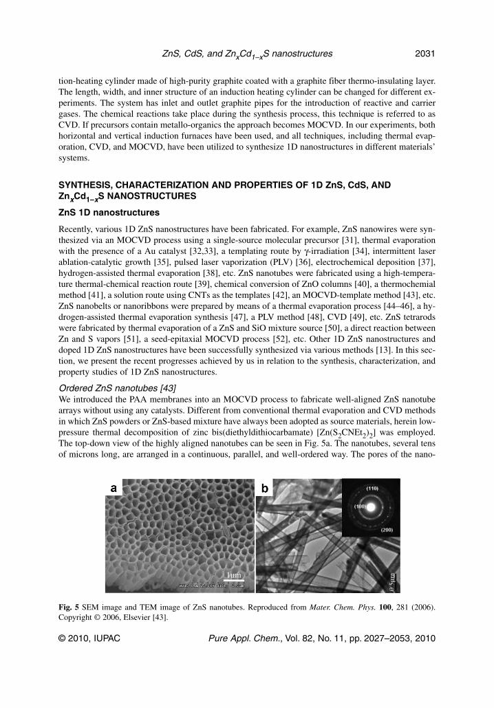
Ordered ZnS nanotubes [43]We introduced the PAA membranes into an MOCVD process to fabricate well-aligned ZnS nanotubearrays without using any catalysts. Different from conventional thermal evaporation and CVD methodsin which ZnS powders or ZnS-based mixture have always been adopted as source materials, herein low-pressure thermal decomposition of zinc bis(diethyldithiocarbamate) [Zn(S2CNEt2)2] was employed.The top-down view of the highly aligned nanotubes can be seen in Fig. 5a. The nanotubes, several tensof microns long, are arranged in a continuous, parallel, and well-ordered way. The pores of the nano -
© 2010, IUPAC Pure Appl. Chem., Vol. 82, No. 11, pp. 2027–2053, 2010
ZnS, CdS, and ZnxCd1–xS nanostructures 2031
Fig. 5 SEM image and TEM image of ZnS nanotubes. Reproduced from Mater. Chem. Phys. 100, 281 (2006).Copyright © 2006, Elsevier [43].
tubes are straight, with a smooth surface and a diameter of ~140–250 nm, which corresponds to the porediameter of the used PAA template. The wall thicknesses of the nanotubes are uniform, and the com-pactness is quite high, about 8.1 × 10⁸ pores/cm2. Transmission electron microscopy (TEM) and se-lected-area electron diffraction (SAED) results show that the nanotubes are polycrystalline, Fig. 5b. Astrong blue–green emission centered at 510 nm is observed. Due to its low temperature and versatility,this MOCVD-template method might present a new and easy approach to fabricate nanotubes from var-ious kinds of sulfides. Such nanotubes grown without catalyst may have promising applications in op-tical, electric, and gas sensing nanodevices [43].
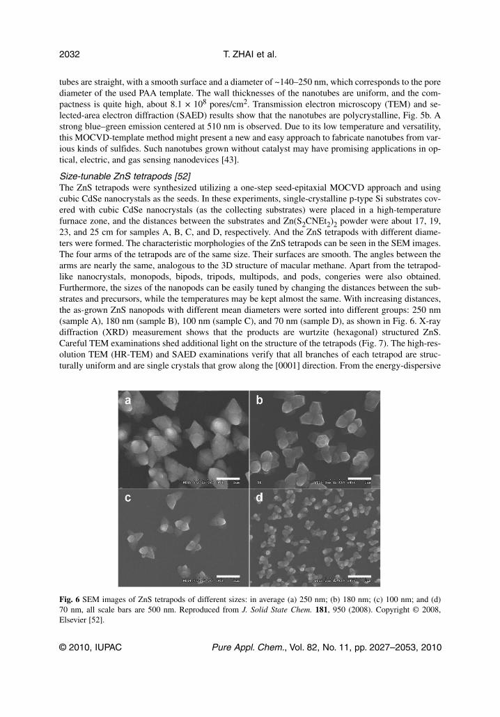
Size-tunable ZnS tetrapods [52]The ZnS tetrapods were synthesized utilizing a one-step seed-epitaxial MOCVD approach and usingcubic CdSe nanocrystals as the seeds. In these experiments, single-crystalline p-type Si substrates cov-ered with cubic CdSe nanocrystals (as the collecting substrates) were placed in a high-temperaturefurnace zone, and the distances between the substrates and Zn(S2CNEt2)2 powder were about 17, 19,23, and 25 cm for samples A, B, C, and D, respectively. And the ZnS tetrapods with different diame-ters were formed. The characteristic morphologies of the ZnS tetrapods can be seen in the SEM images.The four arms of the tetrapods are of the same size. Their surfaces are smooth. The angles between thearms are nearly the same, analogous to the 3D structure of macular methane. Apart from the tetrapod-like nanocrystals, monopods, bipods, tripods, multipods, and pods, congeries were also obtained.Furthermore, the sizes of the nanopods can be easily tuned by changing the distances between the sub-strates and precursors, while the temperatures may be kept almost the same. With increasing distances,the as-grown ZnS nanopods with different mean diameters were sorted into different groups: 250 nm(sample A), 180 nm (sample B), 100 nm (sample C), and 70 nm (sample D), as shown in Fig. 6. X-raydiffraction (XRD) measurement shows that the products are wurtzite (hexagonal) structured ZnS.Careful TEM examinations shed additional light on the structure of the tetrapods (Fig. 7). The high-res-olution TEM (HR-TEM) and SAED examinations verify that all branches of each tetrapod are struc-turally uniform and are single crystals that grow along the [0001] direction. From the energy-dispersive
T. ZHAI et al.
© 2010, IUPAC Pure Appl. Chem., Vol. 82, No. 11, pp. 2027–2053, 2010
2032
Fig. 6 SEM images of ZnS tetrapods of different sizes: in average (a) 250 nm; (b) 180 nm; (c) 100 nm; and (d)70 nm, all scale bars are 500 nm. Reproduced from J. Solid State Chem. 181, 950 (2008). Copyright © 2008,Elsevier [52].
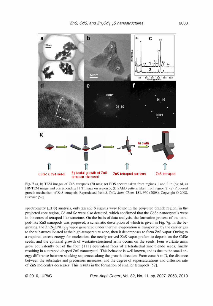
spectrometry (EDS) analysis, only Zn and S signals were found in the projected branch region; in theprojected core region, Cd and Se were also detected, which confirmed that the CdSe nanocrystals werein the cores of tetrapod-like structure. On the basis of data analysis, the formation process of the tetra-pod-like ZnS nanopods was proposed, a schematic description of which is given in Fig. 7g. In the be-ginning, the Zn(S2CNEt2)2 vapor generated under thermal evaporation is transported by the carrier gasto the substrates located at the high-temperature zone, then it decomposes to form ZnS vapor. Owing toa required excess energy for nucleation, the newly arrived ZnS vapor prefers to deposit on the CdSeseeds, and the epitaxial growth of wurtzite-structured arms occurs on the seeds. Four wurtzite armsgrow equivalently out of the four {111} equivalent faces of a tetrahedral zinc blende seeds, finallyresulting in a tetrapod-shaped ZnS nanocrystal. This behavior is well known, and is due to the small en-ergy difference between stacking sequences along the growth direction. From zone A to D, the distancebetween the substrates and precursors increases, and the degree of supersaturations and diffusion rateof ZnS molecules decreases. This results in the formation of smaller tetrapods [52].
© 2010, IUPAC Pure Appl. Chem., Vol. 82, No. 11, pp. 2027–2053, 2010
ZnS, CdS, and ZnxCd1–xS nanostructures 2033
Fig. 7 (a, b) TEM images of ZnS tetrapods (70 nm); (c) EDS spectra taken from regions 1 and 2 in (b); (d, e)HR-TEM image and corresponding FFT image on region 3; (f) SAED pattern taken from region 2; (g) Proposedgrowth mechanism of ZnS tetrapods. Reproduced from J. Solid State Chem. 181, 950 (2008). Copyright © 2008,Elsevier [52].
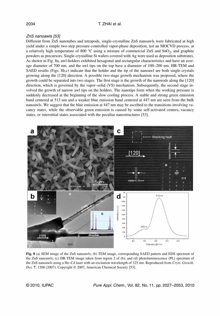
ZnS nanoawls [53]Different from ZnS nanotubes and tetrapods, single-crystalline ZnS nanoawls were fabricated at highyield under a simple two-step pressure-controlled vapor-phase deposition, not an MOCVD process, ata relatively high temperature of 800 °C using a mixture of commercial ZnS and SnO2, and graphitepowders as precursors. Single-crystalline Si wafers covered with Ag were used as deposition substrates.As shown in Fig. 8a, awl-holders exhibited hexagonal and rectangular characteristics and have an aver-age diameter of 700 nm, and the awl tips on the top have a diameter of 100–200 nm. HR-TEM andSAED results (Figs. 8b,c) indicate that the holder and the tip of the nanoawl are both single crystalsgrowing along the [120] direction. A possible two-stage growth mechanism was proposed, where thegrowth could be separated into two stages. The first stage is the growth of the nanorods along the [120]direction, which is governed by the vapor–solid (VS) mechanism. Subsequently, the second stage in-volved the growth of narrow awl tips on the holders. The nanotips form when the working pressure issuddenly decreased at the beginning of the slow cooling process. A stable and strong green emissionband centered at 513 nm and a weaker blue emission band centered at 447 nm are seen from the bulknanoawls. We suggest that the blue emission at 447 nm may be ascribed to the transitions involving va-cancy states, while the observable green emission is caused by some self-activated centers, vacancystates, or interstitial states associated with the peculiar nanostructures [53].
T. ZHAI et al.
© 2010, IUPAC Pure Appl. Chem., Vol. 82, No. 11, pp. 2027–2053, 2010
2034
Fig. 8 (a) SEM image of the ZnS nanoawls; (b) TEM image, corresponding SAED pattern and EDS spectrum ofthe ZnS nanoawls; (c) HR-TEM image taken from region 2 of (b); and (d) photoluminescence (PL) spectrum ofthe ZnS nanoawls using a He–Cd laser with an excitation wavelength of 325 nm. Reproduced from Cryst. Growth.Des. 7, 1388 (2007). Copyright © 2007, American Chemical Society [53].
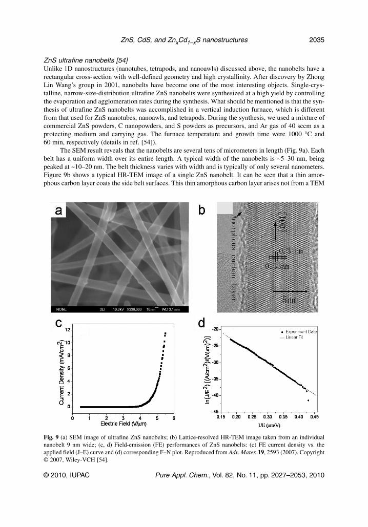
ZnS ultrafine nanobelts [54]Unlike 1D nanostructures (nanotubes, tetrapods, and nanoawls) discussed above, the nanobelts have arectangular cross-section with well-defined geometry and high crystallinity. After discovery by ZhongLin Wang’s group in 2001, nanobelts have become one of the most interesting objects. Single-crys-talline, narrow-size-distribution ultrafine ZnS nanobelts were synthesized at a high yield by controllingthe evaporation and agglomeration rates during the synthesis. What should be mentioned is that the syn-thesis of ultrafine ZnS nanobelts was accomplished in a vertical induction furnace, which is differentfrom that used for ZnS nanotubes, nanoawls, and tetrapods. During the synthesis, we used a mixture ofcommercial ZnS powders, C nanopowders, and S powders as precursors, and Ar gas of 40 sccm as aprotecting medium and carrying gas. The furnace temperature and growth time were 1000 °C and60 min, respectively (details in ref. [54]).
The SEM result reveals that the nanobelts are several tens of micrometers in length (Fig. 9a). Eachbelt has a uniform width over its entire length. A typical width of the nanobelts is ~5–30 nm, beingpeaked at ~10–20 nm. The belt thickness varies with width and is typically of only several nanometers.Figure 9b shows a typical HR-TEM image of a single ZnS nanobelt. It can be seen that a thin amor-phous carbon layer coats the side belt surfaces. This thin amorphous carbon layer arises not from a TEM
© 2010, IUPAC Pure Appl. Chem., Vol. 82, No. 11, pp. 2027–2053, 2010
ZnS, CdS, and ZnxCd1–xS nanostructures 2035
Fig. 9 (a) SEM image of ultrafine ZnS nanobelts; (b) Lattice-resolved HR-TEM image taken from an individualnanobelt 9 nm wide; (c, d) Field-emission (FE) performances of ZnS nanobelts: (c) FE current density vs. theapplied field (J–E) curve and (d) corresponding F–N plot. Reproduced from Adv. Mater. 19, 2593 (2007). Copyright© 2007, Wiley-VCH [54].
mesh, but forms during the belt growth. It serves as a blocker for the belt width and thickness increasemore effectively than for its length increase, since the growth proceeds along the [001] direction of ZnS.This orientation is the fastest and easiest growth direction according to the well-established ZnS crys-tallization kinetics. All these phenomena lead to the ultrafine ZnS nanobelt formation. The nanobeltsgrow along the [001] direction, and typically have no defects, e.g., stacking faults or dislocations. Wehave carried out FE measurements on these ultrafine ZnS nanobelts and found that they possess excel-lent performances: a turn-on field of about 3.47 V/μm at a current density of 10 mA/cm2, and the emis-sion current density of about 11.5 mA/cm2 at a macroscopic field of 5.5 mA/cm2, as shown in Fig. 9c.Figure 9d shows the Fowler–Nordheim (F–N) plot for the nanobelts, which fits well to the line. As ob-tained from the slope of the fitted straight line in Fig. 9d, the nanobelts have a high field-enhancementfactor (β) of 2.01 × 10³. These data suggest that the present nanobelts are highly valuable field emittersthat rival previously reported ZnO, ZnS, Si, SiC, and AlN nanowires/nanobelts and CNT emitters[54,55].
ZnS nanobelt quasi-arrays [44]These quasi-aligned ZnS nanobelt arrays were fabricated through a non-catalytic and template-freethermal evaporation process. They are not only aligned on the micro/macroscopic scales but also dis-play similar crystallographic orientations of their growth axes. The SEM observations reveal that a typ-ical length of the belts is several tens-to-hundreds of micrometers, as shown in Fig. 10a. The belts formin bundles, and within a bundle they are quasi-aligned. In many cases, even perfectly parallel ensem-bles are visible. Figure 10b presents a typical TEM image of an array of parallel nanobelts. The insetshows an SAED pattern from the entire bundle. The similar orientation of all nanobelts within the bun-dle along the [001] direction is documented. HR-TEM images of an individual nanobelt display the de-fect-free (001) lattice plane of wurtzite ZnS with an inter-planar d-spacing of 0.62 nm, suggesting thatthe growth direction is [001]. We have carried out FE measurements on these structures and found thatthey have much improved properties as compared to random nanowires: a low turn-on field(~3.55 V/μm) and a high field-enhancement factor ~1850). The emission characteristic plots are shownin Figs. 10c,d. The emission current density reaches 14.6 mA/cm2 at a macroscopic field of 5.5 V/μm.This value is more that 20 times higher than for randomly distributed ZnS nanobelts. Figure 10d showsvariations of emission current density of a belt ensemble within 4 h under an applied field of 5 V/μm.No notable current density degradation was observed, and the emission current fluctuations were as lowas ~2.6 %, proving the high stability of the ZnS-aligned emitters [44]. To date, there have been only afew reports that deal with FE properties of ZnS nanostructures. Table 2 lists some important FE parameters of 1D ZnS nanostructures reported so far.
T. ZHAI et al.
© 2010, IUPAC Pure Appl. Chem., Vol. 82, No. 11, pp. 2027–2053, 2010
2036
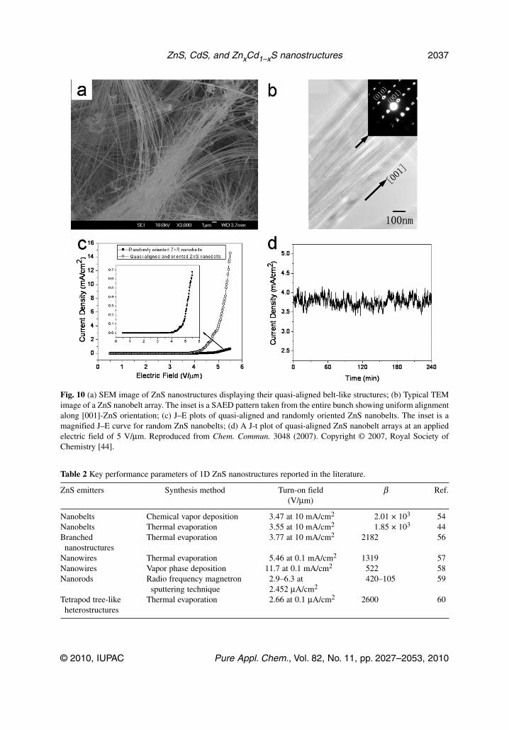
Table 2 Key performance parameters of 1D ZnS nanostructures reported in the literature.
ZnS emitters Synthesis method Turn-on field β Ref.(V/μm)
Nanobelts Chemical vapor deposition 3.47 at 10 mA/cm2 2.01 × 10³ 54Nanobelts Thermal evaporation 3.55 at 10 mA/cm2 1.85 × 10³ 44Branched Thermal evaporation 3.77 at 10 mA/cm2 2182 56nanostructures
Nanowires Thermal evaporation 5.46 at 0.1 mA/cm2 1319 57Nanowires Vapor phase deposition 11.7 at 0.1 mA/cm2 522 58Nanorods Radio frequency magnetron 2.9–6.3 at 420–105 59
sputtering technique 2.452 μA/cm2
Tetrapod tree-like Thermal evaporation 2.66 at 0.1 μA/cm2 2600 60heterostructures
© 2010, IUPAC Pure Appl. Chem., Vol. 82, No. 11, pp. 2027–2053, 2010
ZnS, CdS, and ZnxCd1–xS nanostructures 2037
Fig. 10 (a) SEM image of ZnS nanostructures displaying their quasi-aligned belt-like structures; (b) Typical TEMimage of a ZnS nanobelt array. The inset is a SAED pattern taken from the entire bunch showing uniform alignmentalong [001]-ZnS orientation; (c) J–E plots of quasi-aligned and randomly oriented ZnS nanobelts. The inset is amagnified J–E curve for random ZnS nanobelts; (d) A J-t plot of quasi-aligned ZnS nanobelt arrays at an appliedelectric field of 5 V/μm. Reproduced from Chem. Commun. 3048 (2007). Copyright © 2007, Royal Society ofChemistry [44].
1D CdS nanostructures
Various 1D CdS nanostructures have been synthesized. For example, CdS nanowires were prepared byan MOCVD process [31], a laser-assisted catalytic growth (LCG) method [61], an electrochemical tech-nique [62], a virus-based toolkit [63], thermal evaporation [64], CVD [65], chemical bath deposition[66], electrochemically induced deposition [67], etc. CdS nanotubes were fabricated using a micelle-template-interface reaction route [68], a CVD-template method [69], chemical bath deposition [70], microwave-template synthesis [71], sacrificial template growth [72], etc. CdS nanobelts or nanoribbonswere made through thermal evaporation [73–75], a vapor transport [76], a CVD process [77], PLD [78],etc. Other 1D CdS nanostructures and doped 1D CdS nanostructures have successfully been fabricatedvia various methods [79,80]. In this section, we present the authors’ recent progresses in the synthesis,characterization, and property measurements of 1D CdS nanostructures.
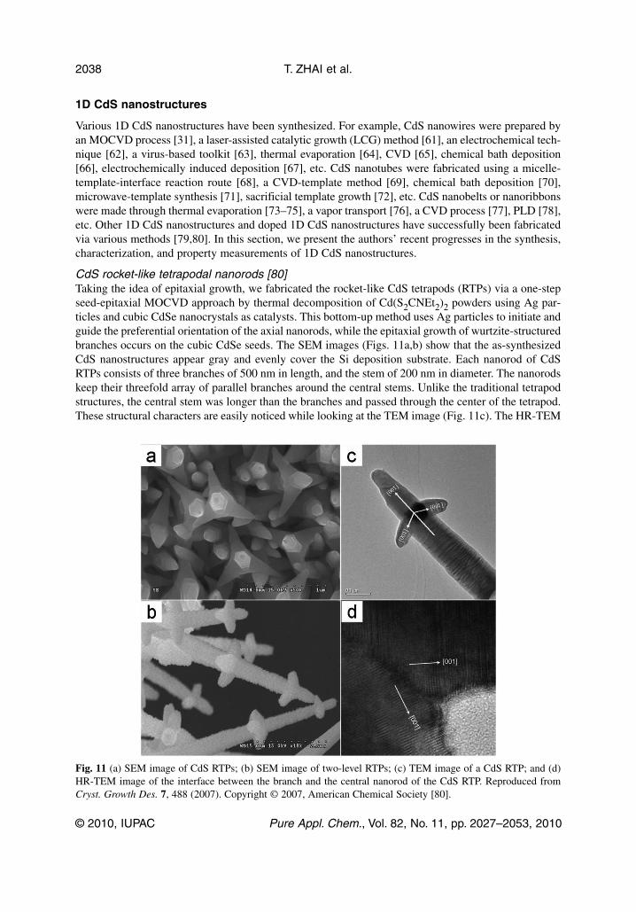
CdS rocket-like tetrapodal nanorods [80]Taking the idea of epitaxial growth, we fabricated the rocket-like CdS tetrapods (RTPs) via a one-stepseed-epitaxial MOCVD approach by thermal decomposition of Cd(S2CNEt2)2 powders using Ag par-ticles and cubic CdSe nanocrystals as catalysts. This bottom-up method uses Ag particles to initiate andguide the preferential orientation of the axial nanorods, while the epitaxial growth of wurtzite-structuredbranches occurs on the cubic CdSe seeds. The SEM images (Figs. 11a,b) show that the as-synthesizedCdS nano structures appear gray and evenly cover the Si deposition substrate. Each nanorod of CdSRTPs consists of three branches of 500 nm in length, and the stem of 200 nm in diameter. The nanorodskeep their threefold array of parallel branches around the central stems. Unlike the traditional tetrapodstructures, the central stem was longer than the branches and passed through the center of the tetrapod.These structural characters are easily noticed while looking at the TEM image (Fig. 11c). The HR-TEM
T. ZHAI et al.
© 2010, IUPAC Pure Appl. Chem., Vol. 82, No. 11, pp. 2027–2053, 2010
2038
Fig. 11 (a) SEM image of CdS RTPs; (b) SEM image of two-level RTPs; (c) TEM image of a CdS RTP; and (d)HR-TEM image of the interface between the branch and the central nanorod of the CdS RTP. Reproduced fromCryst. Growth Des. 7, 488 (2007). Copyright © 2007, American Chemical Society [80].
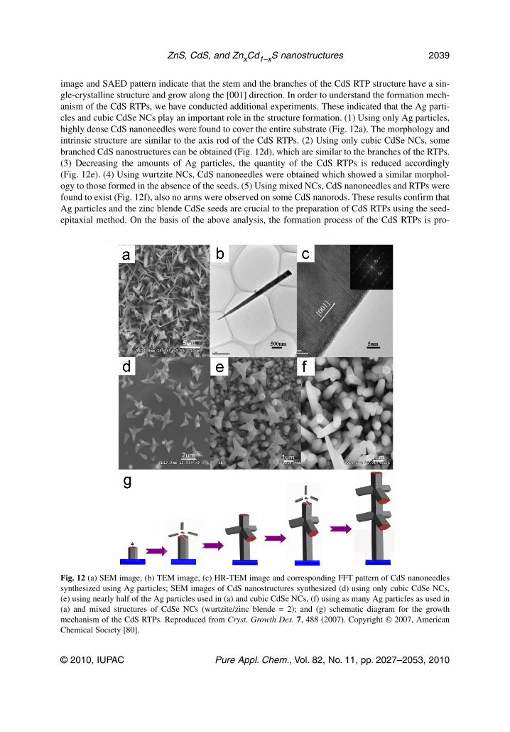
image and SAED pattern indicate that the stem and the branches of the CdS RTP structure have a sin-gle-crystalline structure and grow along the [001] direction. In order to understand the formation mech-anism of the CdS RTPs, we have conducted additional experiments. These indicated that the Ag parti-cles and cubic CdSe NCs play an important role in the structure formation. (1) Using only Ag particles,highly dense CdS nanoneedles were found to cover the entire substrate (Fig. 12a). The morphology andintrinsic structure are similar to the axis rod of the CdS RTPs. (2) Using only cubic CdSe NCs, somebranched CdS nanostructures can be obtained (Fig. 12d), which are similar to the branches of the RTPs.(3) Decreasing the amounts of Ag particles, the quantity of the CdS RTPs is reduced accordingly(Fig. 12e). (4) Using wurtzite NCs, CdS nanoneedles were obtained which showed a similar morphol-ogy to those formed in the absence of the seeds. (5) Using mixed NCs, CdS nanoneedles and RTPs werefound to exist (Fig. 12f), also no arms were observed on some CdS nanorods. These results confirm thatAg particles and the zinc blende CdSe seeds are crucial to the preparation of CdS RTPs using the seed-epitaxial method. On the basis of the above analysis, the formation process of the CdS RTPs is pro-
© 2010, IUPAC Pure Appl. Chem., Vol. 82, No. 11, pp. 2027–2053, 2010
ZnS, CdS, and ZnxCd1–xS nanostructures 2039
Fig. 12 (a) SEM image, (b) TEM image, (c) HR-TEM image and corresponding FFT pattern of CdS nanoneedlessynthesized using Ag particles; SEM images of CdS nanostructures synthesized (d) using only cubic CdSe NCs,(e) using nearly half of the Ag particles used in (a) and cubic CdSe NCs, (f) using as many Ag particles as used in(a) and mixed structures of CdSe NCs (wurtzite/zinc blende = 2); and (g) schematic diagram for the growthmechanism of the CdS RTPs. Reproduced from Cryst. Growth Des. 7, 488 (2007). Copyright © 2007, AmericanChemical Society [80].
posed, a schematic description of which is given in Fig 12g, and detailed growth mechanism is dis-cussed in ref. [80].
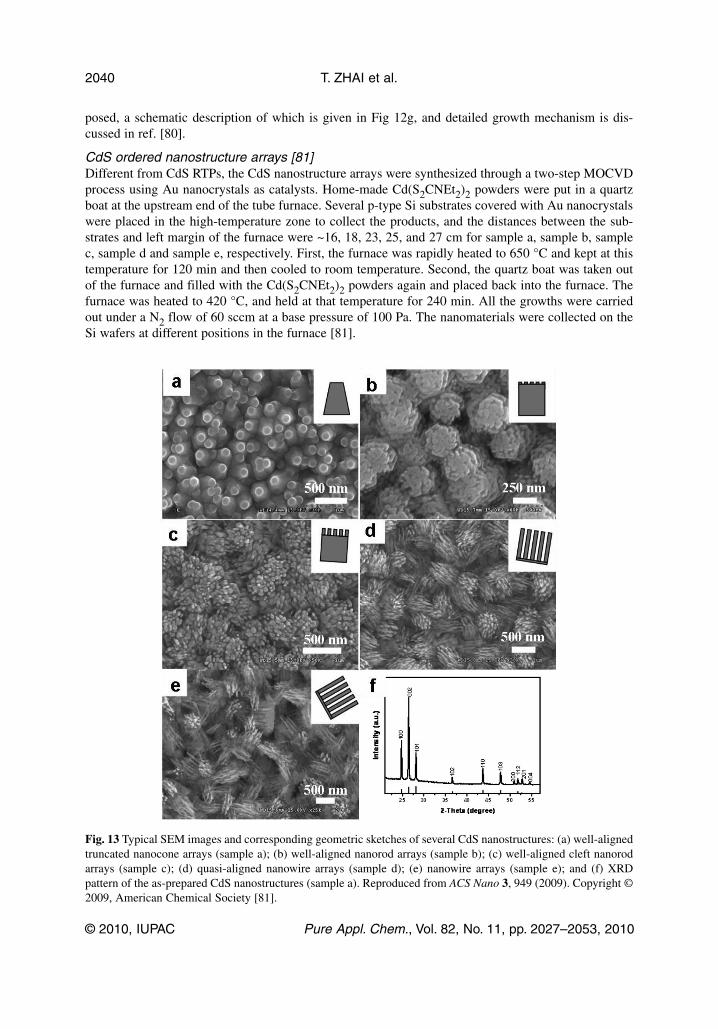
CdS ordered nanostructure arrays [81]Different from CdS RTPs, the CdS nanostructure arrays were synthesized through a two-step MOCVDprocess using Au nanocrystals as catalysts. Home-made Cd(S2CNEt2)2 powders were put in a quartzboat at the upstream end of the tube furnace. Several p-type Si substrates covered with Au nanocrystalswere placed in the high-temperature zone to collect the products, and the distances between the sub-strates and left margin of the furnace were ~16, 18, 23, 25, and 27 cm for sample a, sample b, samplec, sample d and sample e, respectively. First, the furnace was rapidly heated to 650 °C and kept at thistemperature for 120 min and then cooled to room temperature. Second, the quartz boat was taken outof the furnace and filled with the Cd(S2CNEt2)2 powders again and placed back into the furnace. Thefurnace was heated to 420 °C, and held at that temperature for 240 min. All the growths were carriedout under a N2 flow of 60 sccm at a base pressure of 100 Pa. The nanomaterials were collected on theSi wafers at different positions in the furnace [81].
T. ZHAI et al.
© 2010, IUPAC Pure Appl. Chem., Vol. 82, No. 11, pp. 2027–2053, 2010
2040
Fig. 13 Typical SEM images and corresponding geometric sketches of several CdS nanostructures: (a) well-alignedtruncated nanocone arrays (sample a); (b) well-aligned nanorod arrays (sample b); (c) well-aligned cleft nanorodarrays (sample c); (d) quasi-aligned nanowire arrays (sample d); (e) nanowire arrays (sample e); and (f) XRDpattern of the as-prepared CdS nanostructures (sample a). Reproduced from ACS Nano 3, 949 (2009). Copyright ©2009, American Chemical Society [81].
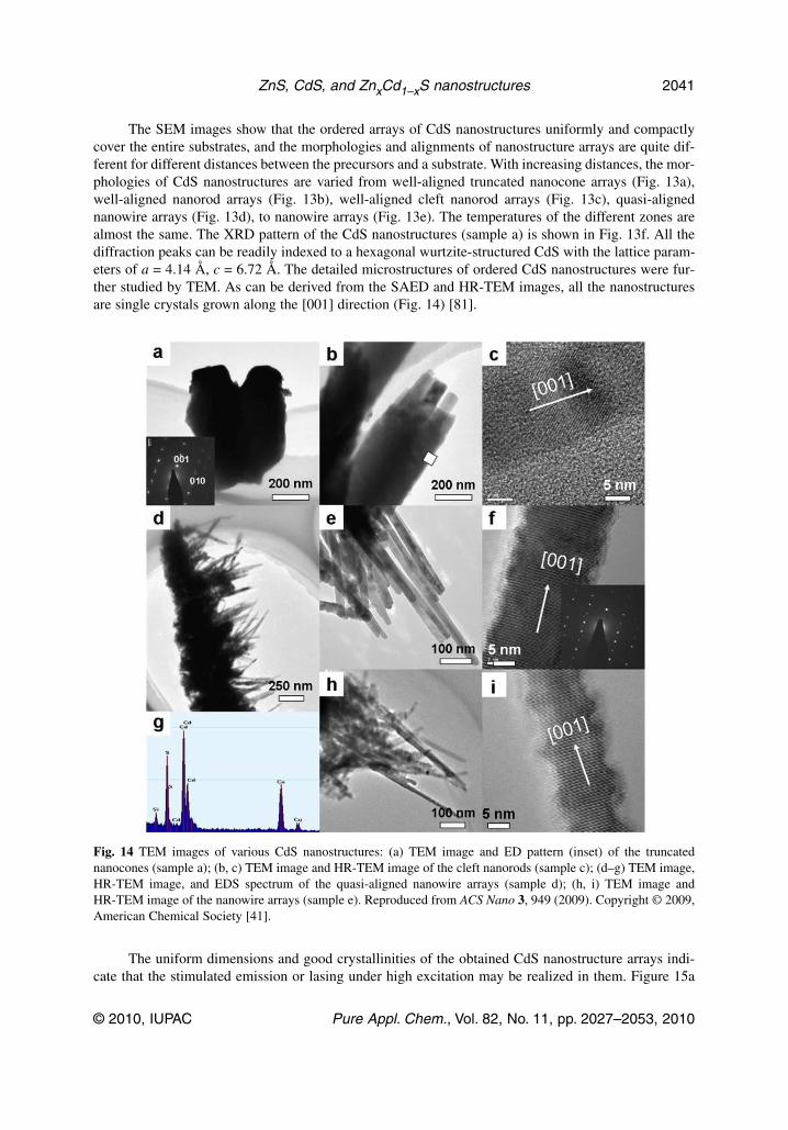
The SEM images show that the ordered arrays of CdS nanostructures uniformly and compactlycover the entire substrates, and the morphologies and alignments of nanostructure arrays are quite dif-ferent for different distances between the precursors and a substrate. With increasing distances, the mor-phologies of CdS nanostructures are varied from well-aligned truncated nanocone arrays (Fig. 13a),well-aligned nanorod arrays (Fig. 13b), well-aligned cleft nanorod arrays (Fig. 13c), quasi-alignednanowire arrays (Fig. 13d), to nanowire arrays (Fig. 13e). The temperatures of the different zones arealmost the same. The XRD pattern of the CdS nanostructures (sample a) is shown in Fig. 13f. All thediffraction peaks can be readily indexed to a hexagonal wurtzite-structured CdS with the lattice param-eters of a = 4.14 Å, c = 6.72 Å. The detailed microstructures of ordered CdS nanostructures were fur-ther studied by TEM. As can be derived from the SAED and HR-TEM images, all the nanostructuresare single crystals grown along the [001] direction (Fig. 14) [81].
The uniform dimensions and good crystallinities of the obtained CdS nanostructure arrays indi-cate that the stimulated emission or lasing under high excitation may be realized in them. Figure 15a
© 2010, IUPAC Pure Appl. Chem., Vol. 82, No. 11, pp. 2027–2053, 2010
ZnS, CdS, and ZnxCd1–xS nanostructures 2041
Fig. 14 TEM images of various CdS nanostructures: (a) TEM image and ED pattern (inset) of the truncatednanocones (sample a); (b, c) TEM image and HR-TEM image of the cleft nanorods (sample c); (d–g) TEM image,HR-TEM image, and EDS spectrum of the quasi-aligned nanowire arrays (sample d); (h, i) TEM image andHR-TEM image of the nanowire arrays (sample e). Reproduced from ACS Nano 3, 949 (2009). Copyright © 2009,American Chemical Society [41].
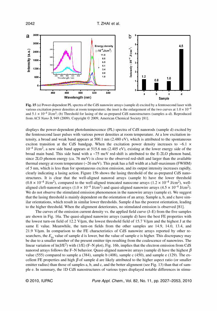
displays the power-dependent photoluminescence (PL) spectra of CdS nanorods (sample d) excited bythe femtosecond laser pulses with various power densities at room temperature. At a low excitation in-tensity, a broad and weak band appears at 500.1 nm (2.480 eV), which is attributed to the spontaneousexciton transition at the CdS bandgap. When the excitation power density increases to ~6.1 ×10⁻⁴ J/cm2, a new side band appears at 515.6 nm (2.405 eV), existing at the lower energy side of thebroad main band. This side band with a ~75 meV red-shift is attributed to the E-2LO phonon band,since 2LO phonon energy (ca. 76 meV) is close to the observed red-shift and larger than the availablethermal energy at room temperature (~26 meV). This peak has a full width at a half-maximum (FWHM)of 5 nm, which is less than for spontaneous exciton emission, and its output intensity increases rapidly,clearly indicating a lasing action. Figure 15b shows the lasing threshold of the as-prepared CdS nano -structures. It is clear that the well-aligned nanorod arrays (sample b) have the lower threshold(0.8 × 10⁻⁴ J/cm2), compared to the well-aligned truncated nanocone arrays (1.2 × 10⁻⁴ J/cm2), well-aligned cleft-nanorod arrays (1.0 × 10⁻⁴ J/cm2) and quasi-aligned nanowire arrays (4.5 × 10⁻⁴ J/cm2).We do not observe the stimulated emission phenomenon in the nanowire arrays (sample e). We suggestthat the lasing threshold is mainly dependent on the orientation of an array. Sample a, b, and c have sim-ilar orientations, which result in similar lower thresholds. Sample d has the poorest orientation, leadingto the higher threshold. When the alignment deteriorates, no stimulated emission is observed [81].
The curves of the emission current density vs. the applied field curve (J–E) from the five samplesare shown in Fig. 16a. The quasi-aligned nanowire arrays (sample d) have the best FE properties withthe lowest turn-on field of 12.2 V/μm, the lowest threshold field of 15.7 V/μm and the highest J at thesame E value. Meanwhile, the turn-on fields from the other samples are 14.9, 14.0, 13.4, and21.9 V/μm. In comparison to the FE characteristics of CdS nanowire arrays reported by other re-searchers, the Eto value of sample d is lower, but the value of sample e is higher. This discrepancy maybe due to a smaller number of the present emitter tips resulting from the coalescence of nanowires. Thelinear variation of ln(J/E2) with (1/E) (F–N plot), Fig. 16b, implies that the electron emission from CdSnanorod arrays follows the F–N behavior. Quasi-aligned nanowire arrays (sample d) have the highest βvalue (555) compared to sample a (384), sample b (408), sample c (450), and sample e (129). The ex-cellent FE properties and high β of sample d are likely attributed to the higher aspect ratio (or smalleremitter radius) than those of samples a, b, and c, and the better alignment (see Fig. 13) than that of sam-ple e. In summary, the 1D CdS nanostructures of various types displayed notable differences in stimu-
T. ZHAI et al.
© 2010, IUPAC Pure Appl. Chem., Vol. 82, No. 11, pp. 2027–2053, 2010
2042
Fig. 15 (a) Power-dependent PL spectra of the CdS nanowire arrays (sample d) excited by a femtosecond laser withvarious excitation power densities at room temperature; the inset is the enlargement of the two curves at 1.0 × 10⁻⁴
and 5.1 × 10⁻⁴ J/cm2; (b) Threshold for lasing of the as-prepared CdS nanostructures (samples a–d). Reproducedfrom ACS Nano 3, 949 (2009). Copyright © 2009, American Chemical Society [81].
lated and FE performances. The stimulated emission strongly correlated with the structure alignment:the better the alignment, the lower the threshold. Both the alignments and aspect ratios greatly affectedthe FE properties: the CdS emitters of higher aspect ratio and better alignment exhibited better FE per-formance. Thus, the well-aligned CdS nanorod arrays had the lower threshold for stimulated emission,and quasi-aligned nanowire arrays produced the higher FE current and possessed the lower turn-onfields [81].
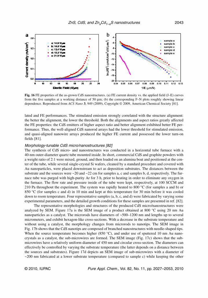
Morphology-tunable CdS micro/nanostructures [82]The synthesis of CdS micro- and nanostructures was conducted in a horizontal tube furnace with a40-nm outer-diameter quartz tube mounted inside. In short, commercial CdS and graphite powders witha weight ratio of 2:1 were mixed, ground, and then loaded on an alumina boat and positioned at the cen-ter of the tube, while several single-crystal Si wafers, cleaned by a standard procedure and covered withAu nanoparticles, were placed downstream to act as deposition substrates. The distances between thesubstrate and the sources were ~20 and ~22 cm for samples a, c and samples b, d, respectively. The fur-nace tube was purged with high-purity Ar for 3 h, prior to heating in order to eliminate any oxygen inthe furnace. The flow rate and pressure inside of the tube were kept, respectively, at 100 SCCM and210 Pa throughout the experiment. The system was rapidly heated to 800 °C (for samples a and b) or850 °C (for samples c and d) in 10 min and kept at this temperature for 30 min before it was cooleddown to room temperature. Four representative samples (a, b, c, and d) were fabricated by varying someexperimental parameters, and the detailed growth conditions for these samples are presented in ref. [82].
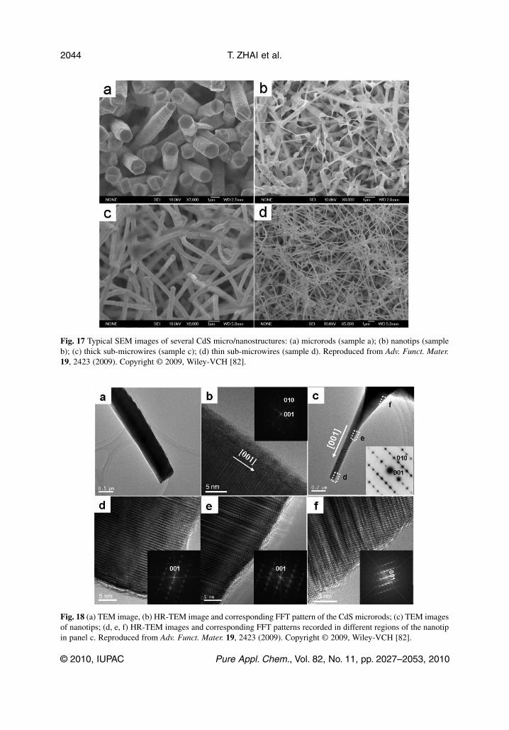
The representative morphologies and structures of the produced CdS micro/nanostructures wereanalyzed by SEM. Figure 17a is the SEM image of a product obtained at 800 °C using 20 nm Aunanoparticles as a catalyst. The microrods have diameters of ~500–1200 nm and lengths up to severalmicrometers, and exhibit hexagon-like cross-sections. With a decrease in the substrate temperature andwithout using a catalyst, the morphology changes from microrods to nanotips. The SEM image inFig. 17b shows that the CdS nanotips are composed of branched nanostructures with needle-shaped tips.When the source temperature becomes higher (850 °C), and under use of sputtered 10 nm Au nano -crystals as a catalyst, the sub-microwires are formed. The SEM image (Fig. 17c) shows that the sub-microwires have a relatively uniform diameter of 450 nm and circular cross-section. The diameters caneffectively be controlled by varying the substrate temperature (the latter depends on a distance betweenthe sources and substrates). Figure 17d depicts an SEM image of sub-microwires with a diameter of~200 nm fabricated at a lower substrate temperature (compared to sample c) while keeping the other
© 2010, IUPAC Pure Appl. Chem., Vol. 82, No. 11, pp. 2027–2053, 2010
ZnS, CdS, and ZnxCd1–xS nanostructures 2043
Fig. 16 FE properties of the as-grown CdS nanostructures. (a) FE current density vs. the applied field (J–E) curvesfrom the five samples at a working distance of 50 μm; (b) the corresponding F–N plots roughly showing lineardependence. Reproduced from ACS Nano 3, 949 (2009), Copyright © 2009, American Chemical Society [81].
T. ZHAI et al.
© 2010, IUPAC Pure Appl. Chem., Vol. 82, No. 11, pp. 2027–2053, 2010
2044
Fig. 17 Typical SEM images of several CdS micro/nanostructures: (a) microrods (sample a); (b) nanotips (sampleb); (c) thick sub-microwires (sample c); (d) thin sub-microwires (sample d). Reproduced from Adv. Funct. Mater.19, 2423 (2009). Copyright © 2009, Wiley-VCH [82].
Fig. 18 (a) TEM image, (b) HR-TEM image and corresponding FFT pattern of the CdS microrods; (c) TEM imagesof nanotips; (d, e, f) HR-TEM images and corresponding FFT patterns recorded in different regions of the nanotipin panel c. Reproduced from Adv. Funct. Mater. 19, 2423 (2009). Copyright © 2009, Wiley-VCH [82].
experimental conditions unchanged. The wire diameters decrease, while the lengths do not change. Thedetailed microstructures of ordered CdS nanostructures were further studied by TEM. As can be derivedfrom the SAED and HR-TEM images, all the nanostructures are single crystals grown along the [001]direction (Fig. 18). For CdS nanotips, the defect concentration decreases toward the tip-end, as shownin Figs. 18d–f. No metal particles are found at the structure tips, thus the growth mechanism of variousCdS nanostructures is attributed to the VS mechanism [82].
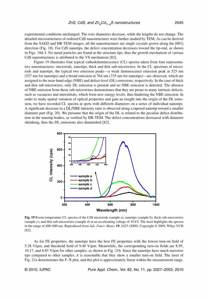
Figure 19 illustrates four typical cathodoluminescence (CL) spectra taken from four representa-tive nanostructures: microrods, nanotips, thick and thin sub-microwires. In the CL spectrum of micro-rods and nanotips, the typical two emission peaks—a weak luminescence emission peak at 525 nm(527 nm for nanotips) and a broad emission at 764 nm (735 nm for nanotips)—are observed, which areassigned to the near-band-edge (NBE) and defect-level (DL) emissions, respectively. In the case of thickand thin sub-microwires, only DL emission is present and no NBE emission is detected. The absenceof NBE emission from these sub-microwires demonstrates that they are prone to many intrinsic defects,such as vacancies and interstitials, which form new energy levels, thus hindering the NBE emission. Inorder to study spatial variation of optical properties and gain an insight into the origin of the DL emis-sion, we have recorded CL spectra at spots with different diameters on a series of individual nanotips.A significant decrease in a DL/NBE intensity ratio is observed along a tapered nanotip toward a smallerdiameter part (Fig. 20). We presume that the origin of the DL is related to the peculiar defect distribu-tion in the nano tip bodies, as verified by HR-TEM. The defect concentrations decreased with diametershrinking, thus the DL emissions also diminished [82].
As for FE properties, the nanotips have the best FE properties with the lowest turn-on field of5.28 V/μm, and threshold field of 9.40 V/μm. Meanwhile, the corresponding turn-on fields are 8.95,10.17, and 8.85 V/μm for other samples, as shown in Fig. 21b. Since the nanotips have much narrowertips compared to other samples, it is reasonable that they show a smaller turn-on field. The inset ofFig. 21a demonstrates the F–N plot, and this plot is approximately linear within the measurement range.
© 2010, IUPAC Pure Appl. Chem., Vol. 82, No. 11, pp. 2027–2053, 2010
ZnS, CdS, and ZnxCd1–xS nanostructures 2045
Fig. 19 Room-temperature CL spectra of the CdS microrods (sample a), nanotips (sample b), thick sub-microwires(sample c), and thin sub-microwires (sample d) at an accelerating voltage of 10 kV. The inset highlights the spectrain the range of 400–600 nm. Reproduced from Adv. Funct. Mater. 19, 2423 (2009). Copyright © 2009, Wiley-VCH[82].
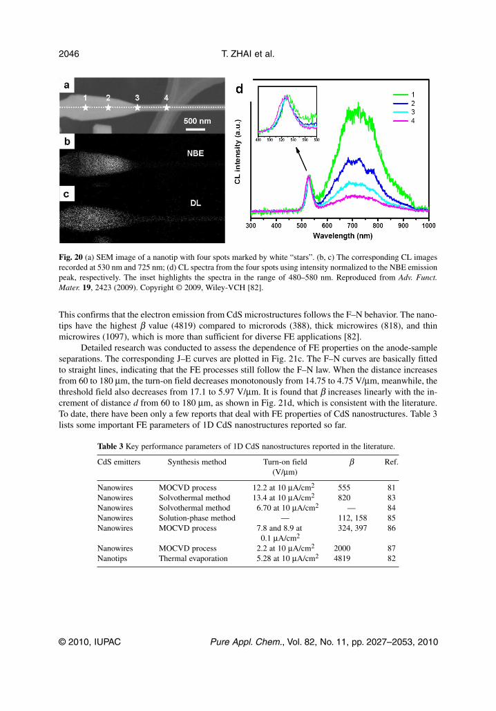
This confirms that the electron emission from CdS microstructures follows the F–N behavior. The nano -tips have the highest β value (4819) compared to microrods (388), thick micro wires (818), and thinmicro wires (1097), which is more than sufficient for diverse FE applications [82].
Detailed research was conducted to assess the dependence of FE properties on the anode-sampleseparations. The corresponding J–E curves are plotted in Fig. 21c. The F–N curves are basically fittedto straight lines, indicating that the FE processes still follow the F–N law. When the distance increasesfrom 60 to 180 μm, the turn-on field decreases monotonously from 14.75 to 4.75 V/μm, meanwhile, thethreshold field also decreases from 17.1 to 5.97 V/μm. It is found that β increases linearly with the in-crement of distance d from 60 to 180 μm, as shown in Fig. 21d, which is consistent with the literature.To date, there have been only a few reports that deal with FE properties of CdS nanostructures. Table 3lists some important FE parameters of 1D CdS nanostructures reported so far.
Table 3 Key performance parameters of 1D CdS nanostructures reported in the literature.
CdS emitters Synthesis method Turn-on field β Ref.(V/μm)
Nanowires MOCVD process 12.2 at 10 μA/cm2 555 81Nanowires Solvothermal method 13.4 at 10 μA/cm2 820 83Nanowires Solvothermal method 6.70 at 10 μA/cm2 — 84Nanowires Solution-phase method — 112, 158 85Nanowires MOCVD process 7.8 and 8.9 at 324, 397 86
0.1 μA/cm2
Nanowires MOCVD process 2.2 at 10 μA/cm2 2000 87Nanotips Thermal evaporation 5.28 at 10 μA/cm2 4819 82
T. ZHAI et al.
© 2010, IUPAC Pure Appl. Chem., Vol. 82, No. 11, pp. 2027–2053, 2010
2046
Fig. 20 (a) SEM image of a nanotip with four spots marked by white “stars”. (b, c) The corresponding CL imagesrecorded at 530 nm and 725 nm; (d) CL spectra from the four spots using intensity normalized to the NBE emissionpeak, respectively. The inset highlights the spectra in the range of 480–580 nm. Reproduced from Adv. Funct.Mater. 19, 2423 (2009). Copyright © 2009, Wiley-VCH [82].
1D ZnxCd1–xS nanostructures
For nano-electronic and -optoelectronic devices, it is very important to fabricate materials with contin-uously tunable physical properties. Recent advances in ternary semiconductor nanocrystals or filmshave shown that their bandgaps and thus their optical emissions can be tuned by changing compoundstoichiometries. Traditional ternary nanostructures are fabricated by physical evaporation depositionmethods or laser ablation-assisted CVD routes [88,89]. These processes involve vapor generation, trans-port, and deposition of target materials. Such practice, however, inevitably requires high temperaturesor high-vacuum laser-ablation operations to generate sufficient amounts of vapor for later deposition.We present a one-step MOCVD approach to prepare single-crystalline ternary ZnxCd1–xS nanocombsand zigzag nanowires at low temperatures using the mixture of Zn(S2CNEt2)2 and Cd(S2CNEt2)2 as thesources. Their constituent stoichiometries can be tuned by changing the relative proportion of the pre-cursors.
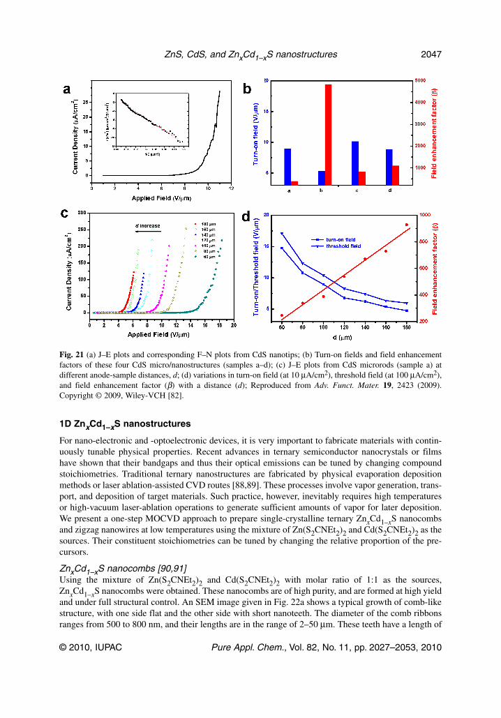
ZnxCd1–xS nanocombs [90,91]Using the mixture of Zn(S2CNEt2)2 and Cd(S2CNEt2)2 with molar ratio of 1:1 as the sources,ZnxCd1–xS nanocombs were obtained. These nanocombs are of high purity, and are formed at high yieldand under full structural control. An SEM image given in Fig. 22a shows a typical growth of comb-likestructure, with one side flat and the other side with short nanoteeth. The diameter of the comb ribbonsranges from 500 to 800 nm, and their lengths are in the range of 2–50 μm. These teeth have a length of
© 2010, IUPAC Pure Appl. Chem., Vol. 82, No. 11, pp. 2027–2053, 2010
ZnS, CdS, and ZnxCd1–xS nanostructures 2047
Fig. 21 (a) J–E plots and corresponding F–N plots from CdS nanotips; (b) Turn-on fields and field enhancementfactors of these four CdS micro/nanostructures (samples a–d); (c) J–E plots from CdS microrods (sample a) atdifferent anode-sample distances, d; (d) variations in turn-on field (at 10 μA/cm2), threshold field (at 100 μA/cm2),and field enhancement factor (β) with a distance (d); Reproduced from Adv. Funct. Mater. 19, 2423 (2009).Copyright © 2009, Wiley-VCH [82].
300–800 nm and a width of 30–100 nm. Additional structure characterization was carried out by usingTEM. A low-magnification image of a comb structure is given in Fig. 22b, which clearly displays theone-side teeth structure of the combs. The front-end of the comb teeth shows no catalytic particles, sug-gesting that the VS mechanism is dominant during the growth process. Figures 22c,d display theHR-TEM images taken in different areas along this array, confirming the monolithically single-crystalnature of the entire comb structure. These also indicate that the comb ribbon grows along the [11–20]directions and the nanoteeth extend along the [0001] directions. The EDS result indicates that the rib-bons and teeth have almost the same compositions, with the atomic ratios (Zn+Cd)/S close to 1. Theformation of the nanocombs is likely involving a two-step growth process: the first one is the fastgrowth based on the VS mechanism and along the [11–20] orientation; this results in the formation ofthe ribbon of the comb; the second one is the subsequent growth of the teeth along the [0001] directionfacilitated by a self-catalyzed process, which can be understood from the structure characteristicspeculiar to the wurtzite family. The formation of one-sided asymmetric nanocombs can be attributed tothe self-catalysis effect of the polar surface. The wurtzite crystal structure has ±(0001) polar surfaces:the (0001) surface is terminated with positively charged Zn or Cd ions and the (000-1) surface is ter-minated with negatively charged S anions, as marked in Fig. 22e. Thus, both positively charged (0001)-Zn or Cd and negatively charged (000-1)-S polar surfaces can be expected. The positively charged Znor Cd (0001) surface is chemically active and the negatively charged S (000-1) is relatively inert, re-sulting in the formation of the comb-teeth along the [0001] orientation as a result of the asymmetricgrowth [90].
ZnxCd1–xS zigzag nanowires [92]While increasing the relative content of Zn(S2CNEt2)2 in the mixed Zn(S2CNEt2)2 and Cd(S2CNEt2)2precursors, ZnxCd1–xS single-crystal zigzag nanowires can be fabricated. These nanowires have lengthsof up to tens of micrometers and a uniform morphology. The SEM image (Fig. 23a) shows that typical
T. ZHAI et al.
© 2010, IUPAC Pure Appl. Chem., Vol. 82, No. 11, pp. 2027–2053, 2010
2048
Fig. 22 (a) SEM image and XRD pattern of ZnxCd1–xS nanocombs; (b) TEM image of a single ZnxCd1–xSnanocomb; (c, d) HR-TEM images recorded in different regions of the comb; (e) Structure model of wurtziteZnxCd1–xS. Reproduced from Chem. Phys. Lett. 427, 371 (2006). Copyright © 2006, Elsevier [90].
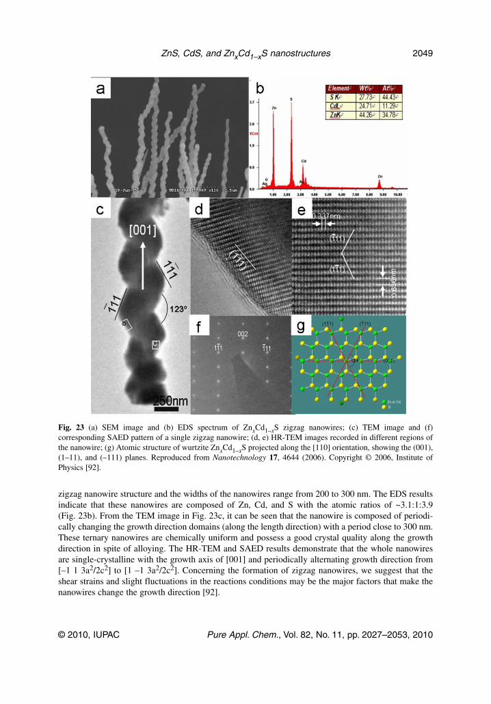
zigzag nanowire structure and the widths of the nanowires range from 200 to 300 nm. The EDS resultsindicate that these nanowires are composed of Zn, Cd, and S with the atomic ratios of ~3.1:1:3.9(Fig. 23b). From the TEM image in Fig. 23c, it can be seen that the nanowire is composed of periodi-cally changing the growth direction domains (along the length direction) with a period close to 300 nm.These ternary nanowires are chemically uniform and possess a good crystal quality along the growthdirection in spite of alloying. The HR-TEM and SAED results demonstrate that the whole nanowiresare single-crystalline with the growth axis of [001] and periodically alternating growth direction from[–1 1 3a2/2c2] to [1 –1 3a2/2c2]. Concerning the formation of zigzag nanowires, we suggest that theshear strains and slight fluctuations in the reactions conditions may be the major factors that make thenanowires change the growth direction [92].
© 2010, IUPAC Pure Appl. Chem., Vol. 82, No. 11, pp. 2027–2053, 2010
ZnS, CdS, and ZnxCd1–xS nanostructures 2049
Fig. 23 (a) SEM image and (b) EDS spectrum of ZnxCd1–xS zigzag nanowires; (c) TEM image and (f)corresponding SAED pattern of a single zigzag nanowire; (d, e) HR-TEM images recorded in different regions ofthe nanowire; (g) Atomic structure of wurtzite ZnxCd1–xS projected along the [110] orientation, showing the (001),(1–11), and (–111) planes. Reproduced from Nanotechnology 17, 4644 (2006). Copyright © 2006, Institute ofPhysics [92].
CONCLUSION AND OUTLOOK
In conclusion, this paper briefly reviews the authors’ recent efforts with respect to the 1D ZnS, CdS,and ZnxCd1–xS nanostructure syntheses using vapor-phase techniques. Five cases of 1D ZnS nano -structures, three cases of 1D CdS nanostructures, and two cases of 1D ZnxCd1–xS nanostructures arediscussed in detail. Future fascinating achievements toward their applications should inspire more re-search efforts to address the fundamental and technological challenges that remain. Needless to say, dueto the tremendous research efforts and the space limitations, this article is unable to cover all the excit-ing works reported in this field.
The investigation of these 1D ZnS and CdS nanostructures will be continuously exciting andhighly rewarding. Undoubtedly, there will be many innovations and developments on the route towardtheir practical integration into nanotechnology and many issues need to be solved before that.
(1) Significant challenges still exist to develop simple, efficient, and inexpensive technology to syn-thesize 1D ZnS and CdS nanostructures; the remaining issues include but are not limited to: reli-able control of diameter, length, orientation, density, crystallization, and hierarchical assembly.
(2) Doping of these nanostructures has become an important issue for widening the range of possibleapplications, in fact, the structure electrical, optical, and magnetic properties can be modified bydoping.
(3) Functional nanodevices, such as field-effect transistors, nanolasers, logic gates, nanosensors, andbiological systems, need to be developed to meet the rapid miniaturization of electronics down tothe nanometer scale.
ACKNOWLEDGMENTS
The authors acknowledge the final support from the Japan Society for the Promotion of Science (JSPS),in the form of a fellowship tenable at the National Institute for Materials Science (NIMS), Tsukuba,Japan (T. Y. Zhai). This work was supported by the International Center for MaterialsNanoarchitectonics (MANA) of the National Institute for Materials Science (NIMS), MEXT, Japan.
REFERENCES
1. C. M. Lieber, Z. L. Wang. MRS Bull. 32, 99 (2007).2. T. Y. Zhai, H. Z. Zhong, Z. J. Gu, A. D. Peng, H. B. Fu, Y. Ma, Y. Y. Li, J. N. Yao. J. Phys. Chem.
C 111, 2980 (2007).3. T. Y. Zhai, Z. J. Gu, Y. Dong, H. Z. Zhong, Y. Ma, H. B. Fu, Y. Y. Li, J. N. Yao. J. Phys. Chem.
C 111, 11604 (2007).4. T. Y. Zhai, X. S. Fang, M. Y. Liao, X. J. Xu, H. B. Zeng, Y. Bando, D. Golberg. Sensors 9, 6504
(2009).5. Y. N. Xia, P. D. Yang, Y. G. Sun, Y. Y. Wu, B. Mayers, B. Gates, Y. D. Yin, F. Kim, H. Q. Yan.
Adv. Mater. 15, 353 (2003).6. X. J. Xu, G. T. Fei, W. H. Yu, X. W. Wang, L. Chen, L. D. Zhang. Nanotechnology 17, 426 (2006).7. G. Z. Shen, J. H. Cho, J. K. Yoo, G. C. Yi, C. J. Lee. J. Phys. Chem. B 109, 9294 (2005).8. Z. L. Wang. ACS Nano 2, 1987 (2008).9. Z. L. Wang. Mater. Sci. Eng. R 64, 33 (2009).
10. X. S. Fang, Y. Bando, U. K. Gautam, T. Y. Zhai, H. B. Zeng, X. J. Xu, M. Y. Liao, D. Golberg.Crit. Rev. Mater. Sci. 34, 190 (2009).
11. X. S. Fang, Y. Bando, D. Golberg. J. Mater. Sci. Technol. 24, 512 (2008).12. D. Moore, Z. L. Wang. J. Mater. Chem. 16, 3898 (2006).13. X. S. Fang, L. D. Zhang. J. Mater. Sci. Technol. 22, 721 (2006).14. P. D. Yang, Y. Y. Wu, R. Fan. Int. J. Nanosci. 1, 1 (2002).
T. ZHAI et al.
© 2010, IUPAC Pure Appl. Chem., Vol. 82, No. 11, pp. 2027–2053, 2010
2050
15. Z. J. Gu, Y. Ma, T. Y. Zhai, B. F. Gao, W. S. Yang, J. N. Yao. Chem.—Eur. J. 12, 7717 (2006).16. Z. J. Gu, T. Y. Zhai, B. F. Gao, G. J. Zhang, D. M. Ke, Y. Ma, J. N. Yao. Cryst. Growth Des. 7,
825 (2007).17. Z. J. Gu, T. Y. Zhai, B. F. Gao, X. H. Sheng, Y. B. Wang, H. B. Fu, Y. Ma, J. N. Yao. J. Phys.
Chem. B 110, 23829 (2006).18. X. Wang, H. B. Fu, A. D. Peng, T. Y. Zhai, Y. Ma, F. L. Yuan, J. N. Yao. Adv. Mater. 21, 1636
(2009).19. L. Y. Zhao, W. S. Yang, Y. Luo, T. Y. Zhai, G. J. Zhang, J. N. Yao. Chem.—Eur. J. 11, 3773
(2005).20. L. Y. Zhao, W. S. Yang, G. J. Zhang, T. Y. Zhai, J. N. Yao. Chem. Phys. Lett. 379, 479 (2003).21. M. Chang, X. L. Cao, X. J. Xu, L. D. Zhang. Phys. Lett. A 372, 273 (2008).22. J. D. Holmes, K. P. Johnston, R. C. Doty, B. A. Korgel. Science 287, 1471 (2000). 23. N. I. Kovtyukhova, T. E. Mallouk, T. S. Mayer. Adv. Mater. 15, 780 (2003).24. B. A. Korgel, D. Fitzmautice. Adv. Mater. 10, 661 (1998).25. D. Li, Y. Wang, Y. Xia. Adv. Mater. 16, 361 (2004).26. Y. Zhao, X. Y. Cao, L. Jiang. J. Am. Chem. Soc. 129, 764 (2007).27. Y. W. Jun, J. S. Choi, J. Cheon. Angew. Chem., Int. Ed. 45, 3414 (2006).28. A. R. Tao, S. Habas, P. D. Yang. Small 4, 310 (2008).29. Y. N. Xia, Y. J. Xiong, B. Lim, S. E. Skrabalak. Angew. Chem., Int. Ed. 48, 60 (2009).30. G. Z. Shen, D. Chen, Y. Bando, D. Golberg. J. Mater. Sci. Technol. 24, 541 (2008).31. C. J. Barrelet, Y. Wu, D. C. Bell, C. M. Lieber. J. Am. Chem. Soc. 125, 11498 (2003).32. Y. W. Wang, L. D. Zhang, C. H. Liang, G. Z. Wang, X. S. Peng. Chem. Phys. Lett. 357, 314
(2002).33. S. Kar, S. Chaudhuri. J. Phys. Chem. B 109, 3298 (2005).34. X. C. Jiang, Y. Xie, J. Lu, L. Y. Zhu, W. He, Y. T. Qian. Chem. Mater. 13, 1213 (2001).35. Y. Jiang, X. M. Meng, J. Liu, Z. R. Hong, C. S. Lee, S. T. Lee. Adv. Mater. 15, 1195 (2003).36. Q. H. Xiong, G. Chen, J. D. Acord, X. Liu, J. J. Zengel, H. R. Gutierrez, J. M. Redwing, L. C.
Lew Yan Voon, B. Lassen, P. C. Eklund. Nano Lett. 4, 1663 (2004).37. J. X. Ding, J. A. Zapien, W. W. Chen, Y. Lifshitz, S. T. Lee. Appl. Phys. Lett. 85, 2361 (2004).38. X. M. Meng, J. Liu, Y. Jiang, W. W. Chen, C. S. Lee, I. Bello. S. T. Lee. Chem. Phys. Lett. 382,
434 (2003).39. L. W. Yin, Y. Bando, J. H. Zhan, M. S. Li, D. Golberg. Adv. Mater. 17, 1972 (2005).40. L. Dloczik, R. Engelhardt, K. Ernst, S. Fiechter, I. Sieber, R. Könenkamp. Appl. Phys. Lett. 78,
3687 (2001).41. Y. C. Zhu, Y. Bando, Y. Uemura, Chem. Commun. 836 (2003).42. H. Zhang, S. Y. Zhang, S. Pan, G. P. Li, J. G. Hou. Nanotechnology 15, 945 (2004).43. T. Y. Zhai, Z. J. Gu, Y. Ma, W. S. Yang, L. Y. Zhao, J. N. Yao. Mater. Chem. Phys. 100, 281
(2006).44. X. S. Fang, Y. Bando, C. H. Ye, D. Golberg. Chem. Commun. 3048 (2007).45. X. S. Fang, Y. Bando, M. Y. Liao, U. K. Gautam, C. Y. Zhi, B. Dierre, B. D. Liu, T. Y. Zhai,
T. Sekiguchi, Y. Koide, D. Golberg. Adv. Mater. 21, 2034 (2009).46. C. Ma, D. Moore, J. Li, Z. L. Wang. Adv. Mater. 15, 228 (2003).47. Y. Jiang, X. M. Meng, J. Liu, Z. Y. Xie, C. S. Lee, S. T. Lee. Adv. Mater. 15, 323 (2003).48. X. D. Li, X. N. Wang, Q. H. Xiong, P. C. Eklund. Nano Lett. 5, 1982 (2005).49. Z. X. Zhang, J. X. Wang, H. J. Yuan, Y. Gao, D. F. Liu, L. Song, Y. J. Xiang, X. W. Zhao, L. F.
Liu, S. D. Luo, X. Y. Dou, S. C. Mou, W. Y. Zhou, S. S. Xie. J. Phys. Chem. C 109, 18352 (2005).50. G. Z. Shen, Y. Bando, J. Q. Hu, D. Golberg. Appl. Phys. Lett. 90, 123101 (2007).51. J. F. Gong, S. G. Yang, H. B. Huang, J. H. Duan, H. W. Liu, X. N. Zhao, R. Zhang, Y. W. Du.
Small 2, 732 (2006).
© 2010, IUPAC Pure Appl. Chem., Vol. 82, No. 11, pp. 2027–2053, 2010
ZnS, CdS, and ZnxCd1–xS nanostructures 2051
52. T. Y. Zhai, Y. Dong, Y. B. Wang, Z. W. Cao, Y. Ma, H. B. Fu, J. N. Yao. J. Solid State Chem. 181,950 (2008).
53. T. Y. Zhai, Z. J. Gu, H. B. Fu, Y. Ma, J. N. Yao. Cryst. Growth Des. 7, 1388 (2007).54. X. S. Fang, Y. Bando, G. Z. Shen, C. H. Ye, U. K. Gautam, P. M. F. J. Costa, C. Y. Zhi, C. C.
Tang, D. Golberg. Adv. Mater. 19, 2593 (2007).55. X. S. Fang, Y. Bando, U. K. Gautam, C. H. Ye, D. Golberg. J. Mater. Chem. 18, 509 (2008).56. X. S. Fang, U. K. Gautam, Y. Bando, B. Dierre, T. Sekiguchi, D. Golberg. J. Phys. Chem. C 112,
4735 (2008).57. S. Biswas, T. Ghoshal, S. Kar, S. Chakrabarti, S. Chaudhuri. Cryst. Growth Des. 8, 2171 (2008).58. Y. Q. Chang, M. W. Wang, X. H. Chen, S. L. Ni, Q. J. Qiang. Solid State Commun. 142, 295
(2007).59. P. K. Ghosh, U. N. Maiti, S. Jana, K. K. Chattopadhyay. Appl. Surf. Sci. 253, 1544 (2006).60. Z. G. Chen, J. Zou, G. Liu, X. D. Yao, F. Li, X. L. Yuan, T. Sekiguchi, G. Q. Li, H. M. Cheng.
Adv. Funct. Mater. 18, 3063 (2008).61. X. F. Duan, C. M. Lieber. Adv. Mater. 12, 298 (2000).62. D. Routkevitch, T. Bigioni, M. Moskovits, J. M. Xu. J. Phys. Chem. 100, 14037 (1996).63. C. B. Mao, D. J. Solis, B. D. Reiss, S. T. Kottmann, R. Y. Sweeney, A. Hayhurst, G. Georgiou,
B. Iverson, A. M. Becher. Science 303, 213 (2004).64. C. H. Ye, G. W. Meng, Y. H. Wang, Z. Jiang, L. D. Zhang. J. Phys. Chem. B 106, 10338 (2002).65. J. P. Ge, Y. D. Li. Adv. Funct. Mater. 14, 157 (2004).66. H. Zhang, X. Y. Ma, J. Xu, J. J. Niu, J. Sha, D. R. Yang. J. Cryst. Growth 246, 108 (2002).67. D. S. Xu, Y. J. Xu, D. P. Chen, G. L. Guo, L. L. Gui, Y. Q. Tang. Adv. Mater. 12, 520 (2000).68. Y. J. Xiong, Y. Xie, J. Yang, R. Zhang, C. Z. Wu, G. A. Du. J. Mater. Chem. 12, 3712 (2002).69. X. P. Shen, A. H. Yuan, F. Wang, J. M. Hong, Z. Xu. Solid State Commun. 133, 19 (2005).70. H. Zhang, X. Y. Ma, J. Xu, D. R. Yang. J. Cryst. Growth 263, 372 (2004).71. M. W. Shao, F. Xu, Y. Y. Peng, J. Wu, Q. Li, S. Y. Zhang, Y. T. Qian. New J. Chem. 26, 1440
(2002).72. X. M. Li, H. B. Chu, Y. Li. J. Solid State Chem. 179, 96 (2006).73. L. F. Dong, J. Jiao, M. Coulter, L. Love. Chem. Phys. Lett. 376, 653 (2003).74. T. Gao, T. H. Wang. J. Phys. Chem. B 108, 20045 (2004).75. Y. K. Liu, J. A. Zapien, C. Y. Geng, Y. Y. Shan, C. S. Lee, Y. Lifshitz, S. T. Lee. Appl. Phys. Lett.
85, 3241 (2004).76. J. Zhang, F. H. Jiang, L. D. Zhang. J. Phys. Chem. B 108, 7002 (2004).77. Z. Q. Wang, J. F. Gong, J. H. Duan, H. B. Huang, S. G. Yang, X. N. Zhao, R. Zhang, Y. W. Du.
Appl. Phys. Lett. 89, 033102 (2006).78. K. Y. Lee, J. R. Lim, H. Pho, Y. J. Choi, K. J. Choi, J. G. Park. Appl. Phys. Lett. 91, 201901
(2007).79. P. V. Radovanovic, C. J. Barrelet, S. Gradečak, F. Qian, C. M. Lieber. Nano Lett. 5, 1407 (2005).80. T. Y. Zhai, Z. J. Gu, H. Z. Zhong, Y. Dong, Y. Ma, H. B. Hu, Y. F. Li, J. N. Yao. Cryst. Growth
Des. 7, 488 (2007).81. T. Y. Zhai, X. S. Fang, Y. Bando, Q. Liao, X. J. Xu, H. B. Zeng, Y. Ma, J. N. Yao, D. Golberg.
ACS Nano 3, 949 (2009).82. T. Y. Zhai, X. S. Fang, Y. Bando, B. Dierre, B. D. Liu, H. B. Zeng, X. J. Xu, Y. Huang, X. L.
Yuan, T. Sekiguchi, D. Golberg. Adv. Funct. Mater. 19, 2423 (2009).83. G. X. Qian, K. F. Huo, J. J. Fu, T. F. Hung, P. K. Chu. J. Appl. Phys. 104, 014312 (2008).84. Q. Tang, X. H. Chen, T. Li, Z. W. Zhao, Y. T. Qian, D. P. Yu, W. C. Yu. Chem. Lett. 33, 1088
(2004).85. H. Y. Li, J. M. Green, J. Jiao. J. Phys. Chem. C 112, 15140 (2008).86. Y. F. Lin, Y. J. Hus, S. Y. Lu, S. C. Kung. Chem. Commun. 2391 (2006).87. Y. F. Lin, Y. J. Hsu, S. Y. Lu, K. T. Chen, T. Y. Tseng. J. Phys. Chem. C 111, 13418 (2007).
T. ZHAI et al.
© 2010, IUPAC Pure Appl. Chem., Vol. 82, No. 11, pp. 2027–2053, 2010
2052
88. Y. K. Liu, J. A. Zapien, Y. Y. Shan, C. Y. Geng, C. S. Lee, S. T. Lee. Adv. Mater. 17, 1372 (2005).89. A. L. Pan, H. Yang, R. B. Liu, R. C. Yu, B. S. Zou, Z. L. Wang. J. Am. Chem. Soc. 127, 15692
(2005).90. T. Y. Zhai, X. Z. Zhang, W. S. Yang, Y. Ma, J. F. Wang, Z. J. Gu, D. P. Yu, H. Yang, J. N. Yao.
Chem. Phys. Lett. 427, 371 (2006).91. X. Z. Zhang, T. Y. Zhai, Y. Ma, J. N. Yao, D. P. Yu. J. Electron Microsc. 57, 7 (2008).92. T. Y. Zhai, Z. J. Gu, W. S. Yang, X. Z. Zhang, J. Huang, Y. S. Zhao, D. P. Yu, H. B. Fu, Y. Ma,
J. N. Yao. Nanotechnology 17, 4644 (2006).
© 2010, IUPAC Pure Appl. Chem., Vol. 82, No. 11, pp. 2027–2053, 2010
ZnS, CdS, and ZnxCd1–xS nanostructures 2053


![2< ' # '9& *#: & ; · QDs (e.g., CdTe-CdS and CdTe-ZnS QDs) were achieved via organic synthesis [3e,f]. It is worth noting that, these orQDs cannot be directly used in bioapplications](https://img.pdfslide.us/doc/110x75/5f4c449da14099768c22651d/2-9-qds-eg-cdte-cds-and-cdte-zns-qds-were-achieved.jpg)