Embed Size (px)
Citation preview

8/3/2019 V200UserManual
http://slidepdf.com/reader/full/v200usermanual 1/171
Qmax Test Equipments (P) Ltd.
Test Director II
UUsseerr’’ssMMaannuuaall

8/3/2019 V200UserManual
http://slidepdf.com/reader/full/v200usermanual 2/171
2

8/3/2019 V200UserManual
http://slidepdf.com/reader/full/v200usermanual 3/171
TEST DIRECTOR II
User’s Manual
Volume - I
© Qmax Test Equipments Ltd.#6,Elcot Avenue, Sholinganallur, Chennai-600 119Phone: (91)-44-24509627 • Fax:(91)-44-24509631
E-mail: [email protected]

8/3/2019 V200UserManual
http://slidepdf.com/reader/full/v200usermanual 4/171
Test Director II User’s Manual
ii
Copyright © 2004. Qmax Test Equipments Pvt. Ltd., India.All rights reservedFebruary 2005, V200
Test Director II™ Interactive Workstation
User’s Manual, Ver. 1.0
Due to continued product development this information may change without notice. Theinformation and intellectual property contained herein is confidential between Qmax TestEquipments Pvt. Ltd and the client and remains the exclusive property of Qmax TestEquipments Pvt. Ltd. If you find any problems in the documentation, please report them tous in writing. Qmax Test Equipments Pvt. Ltd does not warrant that this document is error-free.
No part of this publication may be reproduced, stored in a retrieval system, or transmitted in
any form or by any means, electronic, mechanical, photocopying, recording or otherwisewithout the prior written permission of Qmax Test Equipments Pvt. Ltd.
TestDirector II™ is a trademark of Qmax Test Equipments Pvt. Ltd.
Microsoft® Windows XP is either registered trademark or trademark of MicrosoftCorporation. All other product names or logos mentioned herein are used for identificationpurposes only, and are the trademarks of their respective owners.
Printed in-house at:Qmax Test Equipments Pvt. Ltd.,
E-mail: [email protected]: www.qmaxtest.com
Qmax Test Equipments Pvt. Ltd.
#6,Elcot Avenue, Sholinganallur,Chennai-600 119, Tamil Nadu
IndiaTelephone +91-44-24509627
www.qmaxtest.com

8/3/2019 V200UserManual
http://slidepdf.com/reader/full/v200usermanual 5/171
iii
Revision History
Date Version Description Author
August 2005 1.0 TestDirector II User’s Manual
Volume 1 Interactive WorkStation
Qmax Technical
Writer
8/3/2019 V200UserManual
http://slidepdf.com/reader/full/v200usermanual 6/171
Test Director II User’s Manual
iv
HOW THIS MANUAL IS ORGANIZED
This manual is designed to help you to use and operate TestDirector II InteractiveWorkStation software.
Chapter I: “Introduction to Test Director II” describes the contents and mainfeatures Of Test Director II package. The complete introduction to TestDirector II Is given in brief for clear understanding.
Chapter II: “Introduction to Interactive Workstation” describes the features and
facilities available in the package and the hierarchy
Chapter III: “In circuit Functional Testing” describes how to open in-circuit test
program window and how this In-Circuit Functional Test technique canbe used for repairing the faulty PCBs and also detect the PCB faultsencountered such as short/open circuit conditions, functionally faultydevices, bus faults, fan out problems, wrong placement of devices.
Chapter IV: “Out Circuit Functional Testing” describes how to open Out-circuitFunctional Test program window. The device under test(D.U.T) istaken out of circuit while testing or in isolation. In this testing techniquea out- circuit board must be used to plug in the devices.
Chapter V: “Interactive QSM” describes about a technique called Interactive Qmax
Signature method, which is used for testing the devices by measuringthe nodal impedance. The most important feature is the movablereference nodes. Using this the terminal characteristics between anytwo nodes can be determined i.e. a particular pin’s trace can bedetermined with respect to any other pin rather than GND alone. Thetraces of voltage versus current (V/ I) , voltage versus impedance(V/Z)and voltage versus time(V/T) are stored in a database for comparison
against another board or for analysis.
Chapter VI: “Measurements” describes how to measure the parameters like
Frequency, Inductance, Capacitance, Voltage and Resistance in theInteractive Workstation Window.
Chapter VII: “Oscilloscope” describes about Qmax’s Triple channel oscilloscope,
which is used for waveform analysis.
Chapter VIII: “Open/ Short Testing” describes the techniques used for finding the
opens/ shorts present within the pins of a device/ module/ unit or connectors.
Chapter IX: “Function Generator” describes about Qmax’s Triple Channel Function
Generator feature which helps to generate the user definable wavepatterns or Qmax Standard patterns.
Chapter X: “Boundary Scan Test” describes the Boundary scan method for testing
Boundary scan devices. Chapter XI: “Test Sequencer” describes about the sequencing of tests whereby the
sequence of test programs can be generated.
Chapter XII: “Test Station” describes how to test the program sequenced in Test
Sequencer whereby the selected programs can be tested here.
8/3/2019 V200UserManual
http://slidepdf.com/reader/full/v200usermanual 7/171
v
Table Of Contents
Chapter I Introduction to Test Director II ......................................................I-1 I.1 Main Features of TestDirector II: ...........................................................I-2
I.2 Interactive WorkStation..........................................................................I-3
I.3 TPS Development Studio (Optional)......................................................I-4
I.3.0 Test Station ......................................................................................I-4
I.4 Test Sequencer........................................................................................I-4
I.5 Boundary Scan (Optional) ...................................................................... I-5
I.5.0 Features of Boundary Scan Test Tool ............................................. I-5
I.6 Test Program Set Development Studio Features ..................................I-5
I.6.0 Development of Test program in Test Director II ...........................I-6
I.7 Types of Programs used in Test Director II............................................I-8Chapter II Interactive Workstation ................................................................II.I
II.1 Interactive WorkStation System Flow..................................................II.2
II.2 Interactive Application Features...........................................................II.2
Chapter III In-Circuit Functional Testing ...................................................III-1 III.1 How to: Starting the In-Circuit Testing ............................................ III-2
III.2 Function ............................................................................................ III-4
III.3 Features in the In-Circuit Test Window............................................ III-4
III.3.0 Device Name.............................................................................. III-4
III.3.1 Device List ................................................................................. III-5
III.3.2 Library........................................................................................ III-7
III.3.3 Package ...................................................................................... III-7III.3.4 Threshold.................................................................................... III-7
III.3.5 Time per tick .............................................................................. III-7
III.3.6 Test............................................................................................. III-8
III.3.7 Device Data................................................................................ III-8
III.3.8 Compare ..................................................................................... III-8
III.3.9 Listen.......................................................................................... III-8
III.3.10 Loop Test ................................................................................. III-8III.3.11 Identify ................................................................................... III-11
III.3.12 Procedure for identifying a device ......................................... III-12
III.4 Invoking the Set up Options............................................................ III-15
III.5 Steps to be followed for In-circuit testing....................................... III-16
Chapter IV Out-Circuit Functional Testing.................................................IV-1 IV.1 How to: Starting the Out-Circuit Testing..........................................IV-2
IV.2 Function ............................................................................................ IV-3
IV.3 Features in the Out-Circuit Test Window.........................................IV-4
IV.3.0 Device Name..............................................................................IV-4
IV.3.1 Device List .................................................................................IV-4
IV.3.2 Library........................................................................................IV-6
IV.3.3 Package ......................................................................................IV-6
IV.3.4 Threshold ...................................................................................IV-6
IV.3.5 Time per tick .............................................................................. IV-6IV.3.6 Test.............................................................................................IV-7

8/3/2019 V200UserManual
http://slidepdf.com/reader/full/v200usermanual 8/171
Test Director II User’s Manual
vi
IV.3.7 Device Data................................................................................IV-7
IV.3.8 Compare .....................................................................................IV-7
IV.3.9 Listen..........................................................................................IV-8
IV.3.10 Loop test................................................................................... IV-9
IV.3.11 Identify...................................................................................IV-11
IV.3.12 Procedure for identifying a device .........................................IV-14IV.4 Invoking the Set up Options ...........................................................IV-17
IV.5 Steps to be followed for Out Circuit Testing ..................................IV-18
Chapter V Interactive QSM............................................................................ V-1 V.1 QSM – Concept................................................................................... V-2
V.2 When to use QSM for troubleshooting?.............................................. V-2
V.3 How to: Starting the QSM-VI Test ..................................................... V-2
V.4 Operating Mode................................................................................... V-5
V.5 QSM –VI Interactive window............................................................. V-6
V.6 Step-by-Step Procedure for Interactive mode QSM: ........................V-12
Chapter VI Measurements .............................................................................VI.1
VI.1 How to: Starting the Measurement Parameters................................. VI.2VI.2 Resistance.......................................................................................... VI.3
VI.3 Capacitance .......................................................................................VI.8
VI.4 Voltage............................................................................................ VI.12
VI.5 Inductance .......................................................................................VI.16
VI.6 Frequency........................................................................................VI.20
Chapter VII Open/Short Test ...................................................................... VII.1 VII.1 How to: Starting the Open/Short Test (OST) Window ..................VII.2
VII.2 Description of the OST Measurement Window .............................VII.3
VII.3 Drive Information for testing (OST parameters):...........................VII.5
Chapter VIII Oscilloscope...........................................................................VIII.1 VIII.1 Functional description ..................................................................VIII.2
VIII.2 Measurements...............................................................................VIII.6
Chapter IX Function Generator ....................................................................IX.1 IX.1 A brief description of Function Generator........................................ IX.2
IX.2 Opening the Qmax Function Generator ............................................ IX.3
IX.3 Functional description....................................................................... IX.4
IX.4 Measurement procedure .................................................................... IX.6
Chapter X Boundary Scan Test .......................................................................X.1 X.1 What is Boundary Scan? ......................................................................X.2
X.2 Requirements for Boundary Scan Test Data ........................................X.3
X.3 Procedure for Boundary Scan Test.......................................................X.4X.4 How To: Starting the Boundary Scan Test...........................................X.4
X.5 Test Options .........................................................................................X.5
X.5.0 Opening Boundary Scan path........................................................X.5
X.5.1 Selecting Device Name .................................................................X.6
X.5.2 Selecting Package details ..............................................................X.7
X.5.3 BOM List entry ...........................................................................X.10
X.5.4 Net List Details............................................................................X.11
X.5.5 Saving the Learnt Database.........................................................X.13

8/3/2019 V200UserManual
http://slidepdf.com/reader/full/v200usermanual 9/171
vii
Chapter XI Test Sequencer............................................................................XI.1 XI.1 How to: Starting the Test Sequencer ................................................ XI.2
XI.2 Board Details .................................................................................... XI.5
XI.3 BOM List Details.............................................................................. XI.6
XI.4 Net List Details ................................................................................. XI.7
XI.5 Edge connector.................................................................................. XI.8XI.6 Channel map Mode......................................................................... XI.11
XI.7 Special Options Test Types: ........................................................... XI.23
Chapter XII Board Test Station ...................................................................XII.1 XII.1 Board Test Station ..........................................................................XII.2
XII.2 How to: Starting the Board Test Station.........................................XII.2

8/3/2019 V200UserManual
http://slidepdf.com/reader/full/v200usermanual 10/171

8/3/2019 V200UserManual
http://slidepdf.com/reader/full/v200usermanual 11/171
Chapter I Introduction to Test Director II
8/3/2019 V200UserManual
http://slidepdf.com/reader/full/v200usermanual 12/171
Test Director II User’s Manual
I-2
Introduction
Test Director II (TD II) is Proprietary Test Software for Qmax’s new generation testers. It offers a complete suite of powerful and user-friendly software to complement the provenhardware from Qmax’s range of products for PCB Troubleshooting.
The Test Director II combines the power of Industry Standard test technologies like VHDL (Very High Speed Integrated Circuit Hardware Description Language and BSDL (BoundaryScan Description Language) with the flexibility and extensibility of Python Test Language.
I.1 Main Features of TestDirector II:
Open end Python platform for test application software
VHDL based SIMULATION models for components
Boundary Scan Test Software (BSTS) for testing Boundary Scan devices
Extensive model & test Libraries based on VHDL
User defined Libraries on VHDL & BSDL
Windows Operating System
Industry Standard VHDL simulator for Board simulation
Easy transportability of programs to other systems
The Test Director II suite
The Test Director II suite comprises:
Interactive WorkStation
TPS Development Studio (Optional)
Test Sequencer
Board Test Station

8/3/2019 V200UserManual
http://slidepdf.com/reader/full/v200usermanual 13/171
Introduction to Test DirectorII
I-3
The illustration as shown below brings out the system software flow:
I.2 Interactive WorkStation
The Interactive Workstation covers topics such as In-Circuit Functional Testing (ICFT), Out-Circuit Functional Testing (OCFT), Qmax Signature Method-VI (QSM-VI), Open ShortTesting (OST), Oscilloscope, and Measurement of parameters like Resistance, Voltage,Capacitance, Inductance and Frequency.
Features of Interactive WorkStation
In-Built Design Rule Checker (DRC)
Device pin status check
In- Circuit functional test facility for testing individual IC’s
Out of circuit testing of IC’s
Graphical overview of the device
Click of a button links to detailed data sheets of the device under test
IEEE Standard VHDL library
Industry standard VHDL Simulator to predict the expected output
Response for any digital device. SSI / MSI / LSI / VLSI etc.
Auto compensation is extended for all digital devices
8/3/2019 V200UserManual
http://slidepdf.com/reader/full/v200usermanual 14/171
Test Director II User’s Manual
I-4
Features of Interactive WorkStation
Measurement such as L, C, R, V & F
Open/Short Testing (OST)
Digital Oscilloscope facility while testing
I.3 TPS Development Studio (Optional)
The TPS Development Studio, which is a part of Test Director-II suite, allows the user todevelop, test and debug test programs for boards and devices, all in an IntegratedDevelopment Environment.
The all-new test language is based on the open source Python language.
TPS Development Studio comprises:
Board Testing
Device Testing
Board Test Station is provided for testing the Board programs compiled.
I.3.0 Test Station
Programs developed in Test Director II WorkStation can be exported toTest Station
Only Testing facility by the operator and no program / data / tolerance canbe modified.
For use by operators.
User Defined Error Log reporting, Failure Analysis, statistics and data log.
Network ready for remote monitoring of yield and statistics.
I.4 Test Sequencer
For Sequencing of multiple tests
With conditional branching
Messaging
User prompting
External trigger and external handshake
Board level Test using combination of ICFT, QSM VI, Card Edge Test,Boundary Scan Test
All in one test program

8/3/2019 V200UserManual
http://slidepdf.com/reader/full/v200usermanual 15/171
Introduction to Test DirectorII
I-5
I.5 Boundary Scan (Optional)
Test Director II suite also includes Boundary Scan Tool, which is used to perform boundaryscan test for Boundary Scan (BS) devices in interactive workstation mode. In this testingmode boundary scan cell is the fundamental component of the boundary scan architecture.
This software is optional.
I.5.0 Features of Boundary Scan Test Tool
There is no need for the user to write a separate program.
Devices on board can be tested using the boundary scan chain test.
Automated/Manual generation of SVF using net list and BD files, also, schematic or layout of PCB data can be used.
Fault dictionary of devices can be created from BSD file.
Any Open/Short on device or board can be tested.
Compatibility of execution of program on various ports (USB, PCI, Parallel port).
I.6 Test Program Set Development Studio Features
Net List entry of PCB for diagnosis
PCB overview for component identification.
Schematic Tagging for Net/node follow-up
Test Vector generation for Advanced PCB Programming
Text mode entry & Graphical mode entry
Go-No Go Program edit.
Probe &Check –Learn and Compare facility for Intermediate Nodes in PCB

8/3/2019 V200UserManual
http://slidepdf.com/reader/full/v200usermanual 16/171
Test Director II User’s Manual
I-6
I.6.0 Development of Test program in Test Director II
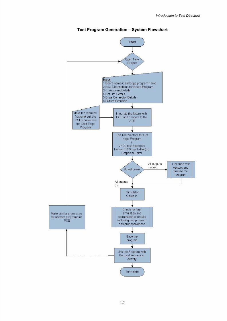
The following steps below describe the various steps to be followed in the development of test program in Test Director II.
1. Open New Project
2. Enter the associated documents if any required
3. Enter the components covered
4. Enter the connectivity or Net list
5. Check for any left out components or connections( Not connectedcomponents)
6. Initialize the PCB
7. Develop test vectors for the inputs
8. Check for drive patterns
9. Debug the program
10. If the program passes save it and use as required
8/3/2019 V200UserManual
http://slidepdf.com/reader/full/v200usermanual 17/171
Introduction to Test DirectorII
I-7
Test Program Generation – System Flowchart

8/3/2019 V200UserManual
http://slidepdf.com/reader/full/v200usermanual 18/171
Test Director II User’s Manual
I-8
I.7 Types of Programs used in Test Director II
There are different programs used in the Test Director II suite. Some of these programs arementioned below:
Go/No Go Program:
Go/No Go Program is made and run by the system to measure the actual response of PCBand compare with the expected response. Based on the result obtained by the response of the PCB Pass/Fail may be declared.
This method will identify quickly whether the board is a good board or a bad board.
In this method all the input pins, Bi-directional pins and output pins are identified and theinput/Bi-directional pins are driven as per the working of the devices which covers thesepins and the expected data will be monitored at the corresponding outputs.
In this program both the input drive pattern and the programmer will provide the expected
output pattern at the particular level. If and only if the expected output matches with theactual output from the device to edge pin the software will display the message as ”BoardPassed “ otherwise software displays ”Board Fails” message.
The corresponding failed edge connector pin will be displayed in the message window withassociated data and the waveform window displays the corresponding waveform with thered color.
The advantage with this method is that the results are Fast and immediate.
This program is generally used to test more number of PCBs.
Diagnostic (Simulation) Program:
The Diagnostic (Simulation) Program is similar to Go/No Go program except that theexpected response predictions are generated for all nodes in a PCB for the purpose of Guided Probe Technique
Learn and Compare method:
The drive pattern driven in the GO/No GO will be converted to drive file using the softwarein text format. Using the net list for the PCB the software will automatically generate the Netand nodes to learn for the program driven. If selected by the programmer, thecorresponding pattern will be stored for the respective node. Programmer can check andverify the same pattern and store the same for reference. Similarly the program is drivenfor all the intermediate nodes and the pattern is stored for the same program. Programmer
can create this database and can visually see the pattern driven in intermediate node. Theprogram is said to be completed when all the intermediate nodes are learned and checked.
As per generated file, the comparator will expect the output taking the input drive patternfrom the Go/No Go file. If the expected output from the simulator and the actual outputcoming from the edges of the board matches, the board passes otherwise board fails.Oncethe program is stored and whenever the PCB is tested, the functionality of the PCB ischecked for its all inputs and outputs. As and when any output fails the softwareautomatically calls for Guided Probe Technique and guides the operator to probe thecorresponding nodes in the PCB. Graphical View of the PCB under test is included as helpfor the operator to locate the components in the PCB. The Software generates Netlist treeand this Netlist tree, which follows further for checking, is also displayed for ease of use.The faulty area is located while probing further and the software stops automatically to
probe further. Automatic and Manual tracking can be enabled by the programmer for hischoice.
8/3/2019 V200UserManual
http://slidepdf.com/reader/full/v200usermanual 19/171
Introduction to Test DirectorII
I-9
Simulator method:
Using Simulator the PCB program made can be made to run and the inputs/outputs faultssimulation can be checked for its correctness.
The drive pattern driven in the GO/NOGO will be converted to drive file using the softwarein text format. Using the net list for the PCB the software will automatically generate theVHDL and Test bench file.
As per generated VHDL file, the simulator will expect the output taking the input drivepattern from the stimulus file. If the expected output from the simulator and the actualoutput coming from the edges of the board matches, the board passes otherwise boardfails.
Cluster Program:
This program is used for an interested area in a PCB for which the program can begenerated and tested. For clusters also the Guided Probe technique can be initiated.
PC(Probe and Compare) Learn And Check:
This method will be useful to find out the fault exactly at a particular node in the PCB butuser should have a good board to learn at each node. The software will guide to probe at allthe nodes on the PCB there by user can learn the whole PCB and learnt data will be storedin the library.
PC check method can be used for testing a fault introduced board / faulty board.The software guides the user to probe at the nodes in the path for the corresponding failure.The tested data will be compared with the learnt data, if both matches the particular nodewill be taken as pass else fail.
In this way software identifies the fault and point to the user exactly where the fault exists.
Summary
This chapter explained the features and facilities incorporated in Test Director II suite for PCB troubleshoot.

8/3/2019 V200UserManual
http://slidepdf.com/reader/full/v200usermanual 20/171

8/3/2019 V200UserManual
http://slidepdf.com/reader/full/v200usermanual 21/171
Chapter II Interactive Workstation
8/3/2019 V200UserManual
http://slidepdf.com/reader/full/v200usermanual 22/171
Introduction
The main purpose of using the Interactive WorkStation suite is to test the Integrated Circuitsand Printed Circuit Boards (PCB’s) for repair and maintenance.
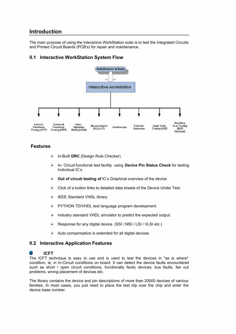
II.1 Interactive WorkStation System Flow
Features
In-Built DRC (Design Rule Checker)
In- Circuit functional test facility using Device Pin Status Check for testingIndividual IC’s
Out of circuit testing of IC’s Graphical overview of the device
Click of a button links to detailed data sheets of the Device Under Test.
IEEE Standard VHDL library.
PYTHON TD/VHDL test language program development.
Industry standard VHDL simulator to predict the expected output.
Response for any digital device. (SSI / MSI / LSI / VLSI etc.)
Auto compensation is extended for all digital devices.
II.2 Interactive Application Features
ICFTThe ICFT technique is easy to use and is used to test the devices in "as is where"condition, ie, in In-Circuit conditions on board. It can detect the device faults encounteredsuch as short / open circuit conditions, functionally faulty devices, bus faults, fan outproblems, wrong placement of devices etc.
The library contains the device and pin descriptions of more than 20000 devices of variousfamilies. In most cases, you just need to place the test clip over the chip and enter thedevice base number.
8/3/2019 V200UserManual
http://slidepdf.com/reader/full/v200usermanual 23/171
Introduction To Interactive Workstation
II.3
V200 can functionally test almost all IC families, making it an ideal choice for PCB repair centers, production line Recovery and Production-line Functional Test Centers. The systemcompensates the drive pattern according to connections of the device in board.
It is designed with custom hybrid drivers to back drive and force a particular test pattern intoa test node for in-circuit testing. The hybrid drivers provide reliability, compactness and
ease of maintenance.
You can interactively test a device: under actual in-circuit conditions, as the device ispresent in a board.
(For example, if an input pin is grounded or linked to an output pin, the system does notdrive that pin.)
In-circuit mode is useful for testing a device under the actual circumstances in which it isgoing to be used in the PCB.
OCFTThe Out-Circuit testing is same as In-Circuit testing, except that the device is taken out of
circuit while testing. The Out-Circuit Tester board must be used for this testing. This boardis provided with a tiny lever operated ZIF (Zero Insertion Force) IC socket (marked asDEVICE) for easy plug-in and plug-out of device. It is provided with Loading Hybrids (oneeach for TTL and CMOS) to load all the pins to facilitate testing of ICs while loaded. Theseact as loads as well as pull-up resistors to the outputs. The appropriate loading hybrid is tobe plugged in respective socket. Please do not use these loads in case if you are testingother logic families like ECL, EIA etc.
In out-circuit mode, the system warns about any short detected between the pins, sincethere cannot be any shorts in out-circuit mode, but continues to drive the pins with their actual test pattern. Out-circuit mode is useful for checking whether the device is actuallybad or not.
Any device tested in Out-circuit must pass the functional test as it is tested in total isolation.Out circuit mode testing can be done for any device before it can be used in the PCB. Thiscan weed out the possibility of using a faulty device during assembly or repair andmaintenance.
QSMIn the Qmax Signature method (QSM), the impedance at a node is measured and isdisplayed on the screen as Voltage versus Current (VI). Also Voltage vs. Time (VT) or Impedance (VZ) is measured automatically.
The nodal impedance analysis can be used equally well for digital nodes (nodes on digitaldevices) and analog nodes (nodes on analog devices and other components). The nodalimpedance analysis can detect the subtle changes in device performance, which are hard
to detect on any oscilloscope or other testing equipment. The changes in deviceperformance can occur due to aging of device or some other causes such as a leakycapacitor or loaded VCC line etc.
Although most of the board / device faults can be detected using ICFT, it is limited to digitalcomponents only. The VI-Trace provides a testing method, which covers all types of devices and is done in power-off condition.
The VI-Trace, unlike ICFT, does not make use of any device programs. Each pin on adevice is considered to be a node and is tested by comparing its traces with that of a gooddevice learnt earlier. It also provides the facility to change the frequency and the amplitudeof the drive signal. The choice of a specific frequency and amplitude is to be madedepending upon the components, which constitute a node. For a reactive node (Capacitiveor Inductive) choosing the right frequency will enhance the VI-Trace in terms of the details.

8/3/2019 V200UserManual
http://slidepdf.com/reader/full/v200usermanual 24/171
Test Director II User’s Manual
II.4
However, for Resistive node, frequency has no much effect. For TTL nodes use of 8Vrange is quite adequate.
Qmax tester provides error %, linear and non-linear methods of comparison for testing eachof the nodes. For Digital TTL ICs the portion above 5.5V and below -0.6V is not of muchsignificance. Hence while testing, it is advisable to use non-linear envelope. But for testing
analog devices, all the portions will have equal importance, and hence Error % or linear comparison mode must be selected.
Patterns are generated as Qmax Library with the specified values. It is made easy to theoperator to select the desired pattern from the Library and drive it into the device under test.However using Function generator facility the operator can program required patterns asnew and store it in the name required and hence new library for Arbitrary waveform patternsalso can be created.
QSM will increase the fault coverage multiple times as it does not use GND alone asreference pin. It selects all combinations by changing the reference pin.
Consider testing a 7400 device having its pin 1 and 2 shorted internally or externally, with
stored VI-Traces of a good 7400 without this pin 1 and 2 shorted. Pins 1 and 2 being highimpedance input pins, their VI-Traces with respect to GND pin will be more or less sameeven if they are shorted together. Thus normal VI-Trace test will pass the device eventhough their pins 1 and 2 shorted. But QSM VI-Trace test will fail the test. QSM will use pin1 as reference and test the remaining pins 2 to 14. This will detect pin 1 and 2 as short andthe test will fail. This is a simple example to show the power of QSM VI-Traces.
Together with ICFT, the VI-Trace test method acts as complementary test strategy to make the available tester an excellent test system to cover all types of board faults.
BST (Optional)
Boundary-scan, as defined by the IEEE Std. 1149.1 standard, is an integrated method for testing interconnects on printed circuit boards that are implemented at the IC level. Thiscapability enables in-circuit testing without the need of bed-of-nail in-circuit test equipment.
OSTOpen Short testing of components or devices on board can be learnt from a Known GoodBoard (KGB) and compared for any similar components in other Board. Diodemeasurements also made possible in this.
Oscilloscope
A ready to use Oscilloscope in V200 having three channels is a very handy tool for the
operator to use.
This Oscilloscope is to be used for measuring TTL signals only.
It combines high bandwidth, fast sampling rates, extensive trigger capabilities and signalprocessing.
This oscilloscope is designed with measurement facility to serve as a range of differentinstruments: oscilloscope, transient recorder, frequency meter and digital voltmeter.
Function Generator
An arbitrary waveform generator has been incorporated to facilitate the waveform
generation as required basis. The required waveforms can be generated, previewed andstored in the user definable database. This can be and used in the application later.

8/3/2019 V200UserManual
http://slidepdf.com/reader/full/v200usermanual 25/171
Introduction To Interactive Workstation
II.5
The Basic Specification of the Function Generator is as follows: -
Amplitude: +/- 13 Volts
Frequency: 500 KHz to 10 MHz.
Samples/Sec: 20 MSPS
Measurement: On Screen mouse click ready to measure
Waveform types: Mathematical, Square, Ramp, Triangle and DC
Resolution: 12 bits
The Function Generator feature helps to generate the user definable wave patterns or Qmax Standard patterns to be selected and driven into the point where it is required.
Measurements
In-circuit measurements of vital parameters of PCB troubleshooting is designed andincorporated in this module to enable the measurements on time and anytime. This is usedto measure the values and interactively the values can be compared for easy access.
Resistance/Capacitance/Inductance/Voltage Measurements
Diode Measurements
Frequency Measurement
Any of these applications can be called in Test Sequencer and learning of the Board can beperformed in Sequencer mode and the Board program can be saved.
Test Station is used to test the above saved Board program using the concerned PCBs.

8/3/2019 V200UserManual
http://slidepdf.com/reader/full/v200usermanual 26/171
Test Director II User’s Manual
II.6

8/3/2019 V200UserManual
http://slidepdf.com/reader/full/v200usermanual 27/171
Chapter III In-Circuit Functional Testing
8/3/2019 V200UserManual
http://slidepdf.com/reader/full/v200usermanual 28/171
Test Director II User’s Manual
III-2
Introduction
The ICFT technique is easy to use and is a widely accepted technique for repairing thefaulty PCBs/devices on board. It can detect the device faults encountered such as short /open circuit conditions, functionally faulty devices, bus faults, fan out problems, wrongplacement of devices etc.
The library contains the device and pin descriptions of more than 20000 devices of variousfamilies. In most cases, you just need to place the test clip over the chip and enter thedevice base number.
V200 can functionally test almost all IC families, making it an ideal choice for PCB repair centers, production line Recovery and Production-line Functional Test Centers.
It is designed with custom hybrid drivers to back drive and force a particular test pattern intoa test node for in-circuit testing. The hybrid drivers provide reliability, compactness andease of maintenance.
You can interactively test a device under actual in-circuit conditions, as the device ispresent in a board, or in out-circuit mode, using the external interface. In in-circuit mode,the system compensates the drive pattern according to the connections of the device.For example, if an input pin is grounded or linked to an output pin, the system does notdrive that pin.
In-circuit mode is useful for testing a device under the actual circumstances in which it isgoing to be used in the PCB.
Opening the In-Circuit Testing
There are two ways you can open the In-Circuit Test program in windows environment.
You can select the Interactive Application program from your Programs menu and click onthe In Circuit button in the Interactive Application window.
Alternatively, you can double click the Interactive Application shortcut icon in your desktopand click on the In Circuit button in the Interactive Application window.
III.1 How to: Starting the In-Circuit Testing
1. To start the In-Circuit Test program window, click on the Start button, and point toPrograms. (Figure 3.1)
2. Point to the folder named Qmax and then click on the Interactive Application icon in
the Test Director II sub-folder. The Interactive Application window opens.(Figure 3.2)
3. After opening the Interactive Application window, click on the In-circuit button in theInteractive Application window. (Figure 3.3)
4. After clicking on the In-Circuit button, the In-Circuit window opens as shown inFigure. (Figure 3.5)

8/3/2019 V200UserManual
http://slidepdf.com/reader/full/v200usermanual 29/171
In-Circuit Functional Testing
III-3
Figure 3.1. Starting the In-Circuit program window
Figure 3.2 Interactive Workstation Windows
Figure 3.3 In-Circuit Icon
Alternatively, to start the In-Circuit Test program window you can Double Click on theInteractive Application shortcut icon (Figure 3.4) on your desktop as shown below.
Figure 3.4 InterActive Application desktop shortcut
After opening the Interactive Application window follow the steps as described above.
Selection
This mode is selected by selecting the In-circuit Icon in the Interactive Workstation MainMenu Icons.

8/3/2019 V200UserManual
http://slidepdf.com/reader/full/v200usermanual 30/171
Test Director II User’s Manual
III-4
Figure 3.5 In-Circuit Device Test Window
III.2 Function
In-circuit mode tests any device selected for its functional program written in the Library and
compares the actual output from the device. When the outputs matches with the expectedoutputs in the Library, the device is declared Passed Functionally ,else fails.
In the In-Circuit mode of testing, if an input pin is connected to Vcc / Gnd or linked to anoutput pin of the same device the system will not drive the input pin, when its linked to anoutput pin.
Corresponding interfaces like clips and probes are to be used to connect the device for test.
III.3 Features in the In-Circuit Test Window
III.3.0 Device Name
Begin testing of device by entering the Base Number of the device printed on the chip suchas DM74LS00P as 7400 simply, in the edit box provided then you choose the package typeof the device from the available package types, which will be listed out, for your convenience.
After completing the above basic information needed, if you want to get the informationabout the device, you can click the Device data button. The information about the device,that is, the pin-out, and the description of each pin is displayed.
Once you test a device, its name gets entered in the drop-down list, so next time you wantto test the same device, you need not enter the device name again; you can simply selectthe device name from the drop-down list.

8/3/2019 V200UserManual
http://slidepdf.com/reader/full/v200usermanual 31/171
In-Circuit Functional Testing
III-5
Figure 3.6. In-Circuit window
Device List Utility
Figure 3.7 Device List Utility Button
This option is provided to list the devices available in the library, for which thefunctional test routines are available in the system database. By default, this optiongives the device library listing provided with the system.
III.3.1 Device List
The database list window provides the facility to list all the devices in the databaseor list specific devices. You can use the following options to display the device list.
If the device could not be found in the list, an error message is displayed. Thedevice list can be printed or stored to a file for further reference.
Apart from giving the list of devices as per the specified category, this option is alsovery useful to find the equivalents or aliases of standard devices.
Device list window-Field Descriptions
Figure 3.8 Field Descriptions (Query Specifications) window
Device NameThis edit box is to enter the Base Number of the device as its name. e.g., DM7474CB canbe entered as 7474 only. If the number to be entered is not clear wildcards like ‘?’ and ‘*’can also be entered to display the devices present in the database. The devices whosenames match with the specified name will be displayed.
In case the device name need not be matched for the current query, make this entry blank.

8/3/2019 V200UserManual
http://slidepdf.com/reader/full/v200usermanual 32/171
Test Director II User’s Manual
III-6
Library You can select the library and test the devices present. The default library is listed asvarious packages such TTL, CMOS, etc., If you have created user Library using your ownnames etc., will be dropped out and you can select the respective libraries.
Package
Select the package type to list the devices of the specified package type present in thedatabase.
No. of Pins Enter the number of pins to list devices having the specified number of pins. Make the entryblank if the number of pins need not be matched for the current query.
Description (Device)Enter the description of the device. When the Query button is clicked, devices having thespecified description would be listed. Even if part of the description string is entered, thematching entries are filtered and listed. If the description need not be matched for thecurrent query, make the entry blank.
Normally, the description is for identifying the device as per its functionality. If query matchtakes place all the devices in the category will be listed out and you can select the deviceyou require to test.
Figure 3.9 Device List dialog box
Include Aliases also in the listing
Tick mark in this selection box, Include Aliases also in this listing, the device list includesthe device name as well as its aliases of similar type devices.
Number of devices foundDisplays the total number of devices that are displayed based on the current query.
CloseUse this to close the dialog box.
SelectThis facility is used to add the selected device from the list displayed to the Device name inthe test window. Click the left mouse button on the device number in the list shown and
press select button, which automatically enter the device number into the Test window.Now you are ready to run the test.

8/3/2019 V200UserManual
http://slidepdf.com/reader/full/v200usermanual 33/171
In-Circuit Functional Testing
III-7
III.3.2 Library
You can select the library and test the devices present in the library. The default library isloaded family wise, like TTL, CMOS etc.,
If any user Library created that also will be dropped out for selection. You can select the
type of Library as per the device program available.
III.3.3 Package
Select the package type of the device that is to be tested. The package type can beDIP(300/600), SIP, PLCC or SOIC, METALCAN.
III.3.4 Threshold
Library
The device test program has its own drive voltage levels and receives threshold levels
defined in the database. When you select the library threshold option, the device is testedusing the threshold defined in the database by default.
User
This facility is provided to the user to select his choice for the threshold setting to test thedevice. At times, the device may fail when tested using the threshold defined in the library.The device’s output could be in the in-between state if the testing was done at criticalthreshold levels. So, it may be required to test the device using a different threshold(loosening the threshold). Selecting the User button does this option. When the User optionis selected, the system prompts you to choose the threshold levels before testing thedevice.
Figure 3.10 Threshold and Time Per Tick dialog box
III.3.5 Time per tick
Library
The test programs for each device has its drive speed defined in the database. When youselect the Library option, the device is driven for testing using the speed defined in thedatabase i.e. default drive speed.
User
This facility is provided to the user to select his choice for the drive speed.
At times, the device may fail when driven using the drive speed defined in the library. Itcould be due to the In-circuit configuration making the device to operate at a lower speed,or if the output pin of the device is loaded with R-C, then its response will be slower than
the normal operating speed. So, it may be required to test the device using a different drivespeed rather than the one defined in the library. This is done by selecting the User button inthe Times per tick selection box.

8/3/2019 V200UserManual
http://slidepdf.com/reader/full/v200usermanual 34/171
Test Director II User’s Manual
III-8
Any change in the Threshold or Times per tick default values will pop up customizeThreshold/Time base menu and the user can select the required values accordingly thenproceed with testing.
III.3.6 Test
Click Test button to start testing the device.
III.3.7 Device Data
To view the device information, click the Device Data button. The pin-out information andthe description of each pin are displayed in the clip window. You can also make a hard copyof the device information if required. Printer icon is placed in the bottom of the window.
III.3.8 Compare
This facility is provided to check similar devices.
By testing one good device, other devices are being compared for its inputs and outputs.This feature will be useful for checking more number of devices.
Fig 3.11 Pin Status Compare Window
III.3.9 Listen
Listen facility is provided to monitor the device activities when the device is powered andwhen the device is not driven with any test pattern. When a device fails the ICFT, thisbutton can be used to check a device just like a logic analyzer. In the Listen mode, the testprogram simply monitors all the ticks.
III.3.10 Loop Test
Loop test button is used to check the consistency / stability of the device under test duringpower on conditions. You are presented with a number of options of how the system has totest the device. You can also set the loop counts with internal pull up /pull down options.

8/3/2019 V200UserManual
http://slidepdf.com/reader/full/v200usermanual 35/171
In-Circuit Functional Testing
III-9
Set Loop Test Conditions
The Loop Test option is provided to check how stable the device behavior is. To test thedevice in a loop, click the button Loop Test. Set Loop Test Conditions dialog boxis displayed (Figure 3.12) and the loop test can be initiated after the various test conditionsare set according to the requirement.
Select tests
Pin Status testsSelecting this option, the loop test checks the Pin status. Pin status checking is done bycomparing the clip status obtained during the first time with the status obtained during thesubsequent times and if they match they are declared pass. Actual functional testing is notdone. This option is good for checking the contact between the DUT and the test clip.
Figure 3.12 Set loop test conditions dialog box
Functional testsSelecting this option, the system takes the clip status only once, but drives the DUT andtests it functionally a number of times as specified by the loop number. This option is usefulin testing intermittent functional failures.
Both the testsSelecting this option, the clip status is done each time before the DUT is functionally tested.
Unconditional loop
Check this option to perform the tests unconditionally the number of times as specified inthe loop count. Checking this disables the Stop at …option.
Stop when
Clip Status compares differentSelect this option to stop the loop test when the clip status condition of the DUT changesduring one test to another test.Clip Status compares sameSelect this option to stop the loop test when the clip status of the DUT is the same during
Loop test.

8/3/2019 V200UserManual
http://slidepdf.com/reader/full/v200usermanual 36/171
Test Director II User’s Manual
III-10
Functional test failsSelect this option to stop the loop test when the functional test performed on the DUT fails.Functional test passesSelect this option to stop the loop test when the functional test performed on the DUTpasses.Functional test compares same
Select this option to stop the loop test when the functional test result performed on the DUTis the same as that of the result performed during the very first time.Functional test compares differentSelect this option to stop the loop test when the functional test result performed on the DUTis different from that of the result when performed during the very first time.
Use Internal pull-up / pull down
If the option Use internal pull-up is checked, then the system uses its internal pull-upresistors while performing the loop test if the device is an open-collector device. Select thisoption, if you not sure the device's output pins have been pulled up or not.
Loop countEnter the number of times the DUT is to be tested.
AbortClick the Abort button, to cancel the operation.
Figure 3.13 Compare Test result window
Proceed
Click the Proceed button, to perform the loop test.
While performing the loop test, when the device fails the very first time due to clock pins,the clock pin termination is performed by displaying the Clock pin termination dialog box.But, when the device passes the very first time and if the device fails in a subsequent test inthe loop, the clock pin termination option is not invoked because all the devices testing inthe loop test mode is with reference to the first device.
8/3/2019 V200UserManual
http://slidepdf.com/reader/full/v200usermanual 37/171
In-Circuit Functional Testing
III-11
III.3.11 Identify
Clicking the Identify button identifies the device by comparing it with the devices in thelibrary. It comes out with a list of possible devices with their identification numbers.
Description
During search of base number of ICs it is experienced that at times the base number of thedevice is not clear or not readable. The Identify option provided in the testing (both In-circuit & Out-circuit) can identify a device by comparing it with the devices in the library. Itcomes out with a list of possible devices with their names.
This feature also helps in testing devices that are not supported in the library, by identifyingthe equivalent devices and using their test routines to test them.
This useful feature can only be used in powered condition and preferably in the in-circuitconditions. The front-end menu is organized in such a manner that the information enteredhelps the program in filtering the devices lists for matching conditions.
Device Identity Window-Field Descriptions
This option provides various fields for the user to enter pertinent details about the device tobe identified. This helps in narrowing down the search for matching conditions, and theresults are also more effective.
PinsEnter the total number of pins for the device to be identified.
PackageSelect the package type (DIP, PLCC or SOIC) from the drop down list.
LibraryThe library selected in the in-circuit / out-circuit mode is displayed initially. Select the libraryfrom the drop list. If the user has developed libraries they can also be selected.
Match floating pins
When a pin floats, it could be an un-connected input or a tri-state output or a bi-directionalpin. This information is used in selective foot print matching (i.e. the pin status of thedevices in the library are matched with the pin details recognized from the clip status, inarriving at the filtered list). With this option enabled, the identify list becomes smaller andhence it can identify the device faster and more accurately.
Check for OC devices and Check for OE devices onlyCheck this option, if the user suspects the device as an OC/OE device. Then thecomparison is made only with the OC/OE devices in the library, resulting in faster and moreaccurate identification.
Check for bus devices onlyCheck this option, if the user suspects the device as a bus device. Then the comparison ismade only with the bus devices in the library, resulting in faster and more accurateidentification.
Check All libraries
This check box selection used to check all the libraries made including the user libraries to
identify the devices. You can check this box for all the times.

8/3/2019 V200UserManual
http://slidepdf.com/reader/full/v200usermanual 38/171
Test Director II User’s Manual
III-12
User custom selections
Custom threshold and Custom time baseUser can select custom threshold to compare for identifying the devices and the time basefor selecting the Library devices in the list. This makes the search faster and the result willbe more accurate to find out correct device.
Similarly User can check the box provided for Internal termination, which is hardwired for selecting any unknown device scrutiny.
Identify the unknown device Click this button to start the identifying process.
Figure 3.14 Identify dialog box
Retest the previous list
Click this button to retest the previous identified device list.
III.3.12 Procedure for identifying a device
Following steps given below can identify the device, taking into account all the guidelinesexplained above.
1. Click the button Identify.
2. The Identify window opens with the default options set.
3. Enter the number of pins for the device to be identified.
4. Select the package type of the device to be identified.
5. Select the library that would probably match the device to be identified.

8/3/2019 V200UserManual
http://slidepdf.com/reader/full/v200usermanual 39/171
In-Circuit Functional Testing
III-13
6. Setting these options and other custom selections are to be checked and click thebutton Identify the unknown device.
7. Then, the clip status of the device is displayed in the Clip Status window. ThePower pins, HIZ pins, the NC pins and the float pins are clearly displayed.
You can confirm the presence of the power pins from the clip status, beforeproceeding further.
Figure 3.15 Confirm action dialog box 8. The devices that match the footprint according to the parameters prefixed earlier are
displayed (Figure 3.16(a)).
Figure 3.16 (a) Matching Footprint with Library
Figure 3.16 (b) Tested Devices Description Window

8/3/2019 V200UserManual
http://slidepdf.com/reader/full/v200usermanual 40/171
Test Director II User’s Manual
III-14
Figure 3.16 (c) Devices that match the footprint dialog
9. From the list displayed, select the devices that match with footprint and press the‘Check’ button to proceed further. Otherwise click the ‘Check all’ button.
Figure 3.17 (a) Testing Device

8/3/2019 V200UserManual
http://slidepdf.com/reader/full/v200usermanual 41/171
In-Circuit Functional Testing
III-15
Fig 3.17(b). Set parameters dialog box
Now the “Set parameters dialog box” (Figure 3.17 (b)) is displayed. By default, the devicesare tested with the system library time base and threshold settings. For testing, if you would
like to define your own time base and threshold settings this dialog box will lead you to edit
palette and drive speed. This is normally done when the devices are not identified with thedefault settings otherwise you can click “Use Default”.
10. In case of OC/OE devices, the user has the option of using pull-up/pull-down featurerespectively, to test the devices.
11. The device is checked and the result is displayed in the “List of identified devices”dialog box as shown in the above figure.
The device will be tested as per the selections made above and the passed list of deviceswill be listed out. Hence you can see the device for which the result tested is passed andthis is the identified device.
Click the ‘Retest the previous list’ to retest the previous identified device list if youhave any doubt to recheck.
III.4 Invoking the Set up Options
Click on the To Set Options button in the Out-Circuit Device Test window in the InteractiveWorkstation suite.
Figure 3.18 To Set Options button
Clicking on To Set Options button opens a new window called Options.

8/3/2019 V200UserManual
http://slidepdf.com/reader/full/v200usermanual 42/171
Test Director II User’s Manual
III-16
Figure 3.19 Setup Options dialog box
The software is made for selection of some optional settings for you, while operating in theIn- circuit mode.
The various options listed in the Options Window are Auto Clipping, Back DrivingDefense Time Limit, Internal Pull-up, Guarding, Listen mode and General options.
Select the general options from General options sub-window.
The General options like BUT should be kept always on while testing.The other options like Scroll to Error, Match LZ to Power, diagnostic Prompt ,Compare Links against Netlist of the Board, Delay for drive pattern after BUT power switched on are provided with control box for Checking and Unchecking.
On selection of the above shown options the selected control will be exhibited duringtesting.
Otherwise the default options will be made through for all device testing. You can makevarious preferences before the testing begins. This facilitates the use of full control of software for different options.
III.5 Steps to be followed for In-circuit testing
1. Click the In Circuit button from the toolbar.
2. The In Circuit mode window opens.
3. Enter the name of the device that is to be tested.
4. To display the details of the device, click the Device Data button.
5. Place the clip on the device that is to be tested.
6. Select the package type for the device that is to be tested.
7. To test the device using the default threshold defined in the library, check the Librarythreshold button. To test the device in the user defined threshold, select the User
button.

8/3/2019 V200UserManual
http://slidepdf.com/reader/full/v200usermanual 43/171
In-Circuit Functional Testing
III-17
8. To test the device using the default time base (times per tick) defined in the library,check the Library time base (times per tick) button. To test the device in the user defined time base (times per tick), select the User button.
9. To test the devices click the Test button.
10. The system starts testing the device, by trying to locate the position of the device in theclip. In case there is any problem auto clipping, the system displays an error message.
11. In case of an output level error, the system prompts for an alternative. The user caneither slow down the drive speed or loosen the threshold level and retry testing.
12. If a device fails due to clock pins, Clock pin terminator dialog box appears listing theclock pins of the BUT with their default values of resistors and voltages. You canchange these values and click the Drive button for the changes to take effect. You canalso skip the termination process by clicking the Skip button. The modified resistanceand voltage values are for the current device and current session and they are notretained for the next device or session.
13. While testing the device, the results of the test are displayed in the message window.
14. Click the Listen button to monitor the device activities when the device is powered andwhen the device is not driven with any test pattern. When a device fails the ICFT, thisbutton can be used to check a device just like a logic analyzer. In the Listen mode, thetest program simply monitors all the ticks.
15. To perform the loop test click the button Loop test. (The Loop test procedure isexplained in the respective section )
16. Clicking the Identify button identifies the device by comparing it with the devices in thelibrary. It comes out with a list of possible devices with their identification numbers. (TheIdentify test procedure is explained in the respective section)
Figure 3.20 Window showing device functionally passed
Summary
In-circuit mode of testing the devices is most widely and frequently used option for
testing troubleshooting the electronic devices. This Chapter has covered all the optionsthat need to be understood for the maximum usage of functions in V200.

8/3/2019 V200UserManual
http://slidepdf.com/reader/full/v200usermanual 44/171
Test Director II User’s Manual
III-18

8/3/2019 V200UserManual
http://slidepdf.com/reader/full/v200usermanual 45/171
Chapter IV Out-Circuit Functional Testing

8/3/2019 V200UserManual
http://slidepdf.com/reader/full/v200usermanual 46/171
Test Director II User’s Manual
IV-2
Introduction
The Out-Circuit testing is basically same as In-Circuit testing, except that the device istaken out of circuit while testing. The Out-Circuit Tester board must be used for this testing.This board is provided with a tiny lever operated ZIF (Zero Insertion Force) IC socket(marked as DEVICE) for easy plug-in and plug-out of device. It is provided with Loading
Hybrids (one each for TTL and CMOS) to load all the pins to facilitate testing of ICs whileloaded. These act as loads as well as pull-up resistors to the outputs. The appropriateloading hybrid is to be plugged in respective socket. Please do not use these loads in caseif you are testing other logic families like ECL, EIA etc.
In out-circuit mode, the system warns about any short detected between the pins, sincethere cannot be any shorts in out-circuit mode, but continues to drive the pins with their actual test pattern. Out-circuit mode is useful for checking whether the device is actuallybad or not.
IV.1 How to: Starting the Out-Circuit Testing
The procedure for opening the Out Circuit test program window is same as that for openingIn Circuit window as explained in Chapter 3.
The figure below shows the Out Circuit icon. Clicking on this button opens the Out CircuitTesting Window.
Figure 4.1. Out-circuit Icon
Figure 4.2. Out-Circuit Window

8/3/2019 V200UserManual
http://slidepdf.com/reader/full/v200usermanual 47/171
Interactive QSM
IV-3
IV.2 Function
This mode of testing is useful for testing devices in the received condition is good or bad.Devices for its functionality can be tested in this mode. The devices are to be plugged ininto the ZIF adaptor and locked with the pin 1 of the device in the marked position. VCCand GND connection jumpers are to be placed as per the device data pin connections. The
Out-Circuit board is to be used for this testing.
Figure 4.3. Out-Circuit Board This board is provided with a tiny lever operated ZIF (Zero Insertion Force) IC socket(marked as DEVICE) for easy plug-in and plug-out of device. It is provided with LoadBoards (one each for TTL and CMOS) to load all the pins to facilitate testing of ICs whiletesting. This board act as loads as well as pull-up resistors to the outputs. The appropriateloading board is to be plugged in at J3 socket. The test cable is to be plugged-in at socketsJ1 and J2.
The out-circuit board is powered by plugging-in the power connector at J6 and tapping thepower from the front panel at device power terminals. The device is powered by setting the
jumpers on the two SIP connectors (J4 and J5). These connectors have three vertical rowsof pins. The pins in the middle row of J5 (second) are wired to the left half of the ZIF socket.The pins in the middle row of J4 are wired to the right half of the ZIF socket. All the pins inthe left row (first) of J4 and J5 are connected to VCC whereas all the pins in the right row(third) are connected to GND.
To connect a pin of device to VCC, the jumper should be placed in the left position (linkingrows 1&2). To connect a pin to GND, the jumper should be placed in the right position(linking rows 2&3). Any good device, when tested for out-circuit, must pass the functionaltest as it is tested in total isolation.

8/3/2019 V200UserManual
http://slidepdf.com/reader/full/v200usermanual 48/171
Test Director II User’s Manual
IV-4
When a device is reported to fail the in-circuit test, after checking the possible causes, it isalways advisable to test it in out-circuit mode before declaring the device as faulty. This willconfirm the device failure and help the troubleshooting to be in the right direction.
Out-circuit can also be used to test any device, before it can be used in the circuit. Thishelps to weed out the possibility of using a faulty device during a circuit board assembly.
IV.3 Features in the Out-Circuit Test Window
Figure 4.4 Out-Circuit Test WindowIV.3.0 Device Name
Begin testing of device by entering the Base Number of the device printed on the chip suchas DM74LS00P as 7400 simply, in the edit box provided then you choose the package typeof the device from the available package types, which will be listed out, for your convenience.
After completing the above basic information needed, If you want to get the informationabout the device, you can click the Device data button. The information about the device,that is, the pin-out, and the description of each pin is displayed.
Once you test a device, its name gets entered in the drop-down list, so next time you wantto test the same device, you need not enter the device name again; you can simply selectthe device name from the drop-down list.
Device List Utility button
Figure 4.5 Device List Utility Button
This option is provided to list the devices available in the library, for which the functional testroutines are available in the system database. By default, this option gives the devicelibrary listing provided with the system.
IV.3.1 Device List
The Device list(Fig.4.6) provides the facility to list all the devices in the Library.
You can use the following options to display the device list. If the device could not be foundin the list, an error message is displayed. The device list can be printed or stored to a file for further reference.Apart from giving the list of devices as per the specified category, this option is also veryuseful to find the equivalents or aliases of standard devices.
8/3/2019 V200UserManual
http://slidepdf.com/reader/full/v200usermanual 49/171
Interactive QSM
IV-5
Device List Window-Field Descriptions
Device NameEnter the name of the device. Wildcards like ‘?’ and ‘*’ can also be entered to display thedevices present in the database. The devices whose names match with the specified namewill be displayed. The usage for the wildcard option is the same as for the DOS command
“DIR”. In case the device name need not be matched for the current query, make this entryblank.
PackageSelect the package type to list the devices of the specified package type present in thedatabase.
Pins Enter the number of pins to list devices having the specified number of pins.
Make the entry blank, if the no. of pins need not be matched for the current query.
Description of device Enter the description of the device. When the Query button is clicked, devices having thespecified description would be listed. Even if part of the description string is entered, thematching entries are filtered and listed. If the description need not be matched for thecurrent query, make the entry blank.
Figure 4.6 Device List dialog box
Include Aliases also in the listing Selecting the Include Aliases button, the device list includes the device name as well as itsaliases.
Number of devices found
Displays the total number of devices that are displayed based on the current query.
SelectThis facility is used to add the selected device from the list displayed to the Device name inthe test window. Click the left mouse button on the device number in the list shown and
press select button, which automatically enter the device number into the Test window.Now you are ready to run the test.

8/3/2019 V200UserManual
http://slidepdf.com/reader/full/v200usermanual 50/171
Test Director II User’s Manual
IV-6
CloseUse this to close the dialog box.
IV.3.2 Library
You can select the library and test the devices present in the library. It is not possible for you to create a new library in WorkStation. Creating a library can only be done in IDDE. Thedefault library in WorkStation is QMAX.
IV.3.3 Package
Select the package type of the device that is to be tested. The package type can be DIP300or DIP600 or SIP or PLCC or SOIC, etc.
IV.3.4 Threshold
Library
The device test program has its own drive voltage levels and receives threshold levelsdefined in the database. When you select the library threshold option, the device is testedusing the threshold defined in the database by default.
User
This facility is provided to the user to select his choice for the threshold setting to test thedevice. At times, the device may fail when tested using the threshold defined in the library.The device’s output could be in the in-between state if the testing was done at critical
threshold levels. So, it may be required to test the device using a different threshold(loosening the threshold). Selecting the User button does this option. When the User optionis selected, the system prompts you to choose the threshold levels before testing thedevice.Normally the user defined threshold settings need not to be done for out circuit testing.
Figure 4.7 Threshold and Times Per Tick Dialog Box
IV.3.5 Time per tick
Library
The test programs for each device has its drive speed defined in the database. When youselect the Library option, the device is driven for testing using the speed defined in thedatabase i.e. default drive speed.

8/3/2019 V200UserManual
http://slidepdf.com/reader/full/v200usermanual 51/171
Interactive QSM
IV-7
User
This facility is provided to the user to select his choice for the drive speed.
At times, the device may fail when driven using the drive speed defined in the library. It
could be due to the In-circuit configuration making the device to operate at a lower speed,or if the output pin of the device is loaded with R-C, then its response will be slower thanthe normal operating speed. So, it may be required to test the device using a different drivespeed rather than the one defined in the library. This is done by selecting the User button inthe Times per tick selection box.
Any change in the Threshold or Times per tick default values will pop up customizeThreshold/Time base menu and the user can select the required values accordingly thenproceed with testing.
Generally the time base is defined in the library for all the devices. If required only, the user has to select different time base and test the devices in out circuit.
IV.3.6 Test
Click the Test button to start testing the device.
IV.3.7 Device Data
To get the device information, click the Device Data button. The pin-out information and thedescriptions of each pin are displayed in the clip window. You can also print the deviceinformation, if required for which the printer icon is provided in the device data window.
Figure 4.8 Device Data Window
IV.3.8 Compare
This facility is provided to check similar devices.
By testing one good device, other devices are being compared for its inputs and outputs.This feature will be useful for checking more number of devices.

8/3/2019 V200UserManual
http://slidepdf.com/reader/full/v200usermanual 52/171
Test Director II User’s Manual
IV-8
Figure 4.9 Pin Status Compare Window
Figure 4.10 Device Comparison Same Window
IV.3.9 Listen
The Listen facility is provided to monitor the device activities when the device is powered.Also no drive patterns will be driven into the device.
This facility may be used to check a device just like a logic analyzer. In the Listen mode, thetest program simply monitors all the ticks, which can be driven.

8/3/2019 V200UserManual
http://slidepdf.com/reader/full/v200usermanual 53/171
Interactive QSM
IV-9
Figure 4.11 Listen Facility Window
IV.3.10 Loop test
To confirm the device test status, this facility Loop test to be used. Clicking the Loop testbutton, the system performs loop test mode, where it displays the Set Loop test conditionsdialog. You are presented with a number of options of loop test to be carried out.
Set Loop Test conditions
Figure 4.12 Set loop test conditions dialog box
Set Loop Test Conditions dialog box is displayed and the loop test can be initiated after thevarious test conditions are set according to the requirement.
Select tests
Clip Status tests
Selecting this option, the loop test checks the clip status. Comparing the clip statusobtained during the first time with the status obtained during the subsequent times does clipstatus checking and if they match they are declared pass. Actual functional testing is notdone. This option is good for checking the contact between the device and the test clip.

8/3/2019 V200UserManual
http://slidepdf.com/reader/full/v200usermanual 54/171
Test Director II User’s Manual
IV-10
Functional testsSelecting this option, the system takes the clip status only once, but drives the device andtests it functionally a number of times as specified by the loop number. This option is usefulin testing intermittent functional failures.
Both the tests Selecting this option, the clip status is done each time before the device is functionallytested.
Unconditional loop
Check this option to perform the tests unconditionally the number of times as specified inthe loop count. Checking this disables the Stop at option.
Stop when
Clip Status compares different
Select this option to stop the loop test when the clip status of the device compares different.
Clip Status compares sameSelect this option to stop the loop test when the clip status of the device compares same.
Functional test failsSelect this option to stop the loop test when the functional test performed on the devicefails.
Functional test passesSelect this option to stop the loop test when the functional test performed on the devicepasses.
Functional test compares sameSelect this option to stop the loop test when the functional test result performed on thedevice is the same as that of the result performed during the very first time.
Functional test compares differentSelect this option to stop the loop test when the functional test result performed on thedevice is different as that of the result when performed during the very first time.
Use Internal pull-up / pull down
If the option Use internal pull-up is checked, then the system uses its internal pull-upresistors while performing the loop test if the device is an open-collector device. Select thisoption, if the user is not sure if the device's output pins have been pulled up or not.
Loop count
Enter the number of times the device is to be tested.
AbortClick the Abort button, to cancel the current operation.
ProceedClick the Proceed button, to perform the loop test.
While performing the loop test, when the device fails the very first time due to clock pins,
the clock pin termination is performed by displaying the Clock pin termination dialog box.But, when the device passes the very first time and if the device fails in some others the

8/3/2019 V200UserManual
http://slidepdf.com/reader/full/v200usermanual 55/171
Interactive QSM
IV-11
clock pin termination option is not invoked, since all the devices testing in the loop testmode is with reference to the first device.
Figure 4.13 Loop test result dialog box
IV.3.11 Identify
Clicking the Identify button identifies the device by comparing it with the devices in thelibrary. It comes out with a list of possible devices with their identification numbers.
Figure 4.14 Device Identify Window
Description
During search of base number of ICs it is experienced that at times the base number of thedevice is not clear or not readable. The Identify option provided in the testing (both In-circuit & Out-circuit) can identify a device by comparing it with the devices in the library. Itcomes out with a list of possible devices with their names.
This feature also helps in testing devices, which are not supported in the library, by
identifying the equivalent devices and using their test routines to test them.
8/3/2019 V200UserManual
http://slidepdf.com/reader/full/v200usermanual 56/171
Test Director II User’s Manual
IV-12
This useful feature can only be used in powered condition and preferably in the in-circuitconditions. The front-end menu is organized in such a manner that the information enteredhelps the program in narrowing down (filtering) the devices lists for matching conditions.
Device identity window-Field Descriptions This option provides various fields for you to enter pertinent details about the device to be
identified. This helps in narrowing down the search for matching conditions, and the resultsare also more effective.
Pins Enter the total number of pins for the device to be identified.
Figure 4.15 Identify dialog box
Figure 4.16 Align clip message box
Package Select the package type (DIP, PLCC or SOIC) from the drop down list.
Match floating pinsWhen a pin floats, it could be an un-connected input or a tri-state output or a bi-directionalpin. This information is used in selective foot print matching (i.e. the pin status of thedevices in the library are matched with the pin details recognized from the clip status, inarriving at the filtered list). With this option enabled the identify list is smaller and hence itcan identify faster and more accurately.

8/3/2019 V200UserManual
http://slidepdf.com/reader/full/v200usermanual 57/171
Interactive QSM
IV-13
Figure 4.17 Devices Matching with the Footprint Message Box
Check for OC/OE devices only Check this option, if you suspect the device as an OC/OE device. Then the comparison ismade only with the OC/OE devices in the library, resulting in faster and more accurateidentification.
Check for bus devices onlyCheck this option, if the user suspects the device as a bus device. Then the comparison ismade only with the bus devices in the library, resulting in faster and more accurateidentification.
Check all librariesThis check box selection used to check all the libraries made including the user libraries toidentify the devices. You can check this box for all the times.
Custom threshold and Custom time base User can select custom threshold to compare for identifying the devices and the time basefor selecting the Library devices in the list. This makes the search faster and the result willbe more accurate to find out correct device.
Use internal termination Similarly User can check the box provided for Internal termination, which is hardwired for selecting any unknown device scrutiny.
Identify the unknown deviceClick this button to start the identifying process.
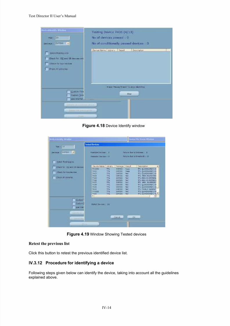
8/3/2019 V200UserManual
http://slidepdf.com/reader/full/v200usermanual 58/171
Test Director II User’s Manual
IV-14
Figure 4.18 Device Identify window
Figure 4.19 Window Showing Tested devices
Retest the previous list
Click this button to retest the previous identified device list.
IV.3.12 Procedure for identifying a device
Following steps given below can identify the device, taking into account all the guidelinesexplained above.

8/3/2019 V200UserManual
http://slidepdf.com/reader/full/v200usermanual 59/171
Interactive QSM
IV-15
1. Click the button Identify.
2. The Identify window opens with the default options set.
3. Enter the number of pins for the device to be identified.
4. Select the package type of the device to be identified.
5. Select the library that would probably match the device to be identified.
6. Setting these options and other custom selections are to be checked and click thebutton Identify the unknown device. The system prompts to align clip’s pin 1 todevice’s pin1.
7. Then, the clip status of the device is displayed in the Clip Status window. The Power pins, HIZ pins, the NC pins and the float pins are clearly displayed.
You can confirm the presence of the power pins from the clip status, before proceedingfurther. (Figure 4.20)
Figure 4.20 Confirm action dialog box
8. The devices that match the footprint according to the parameters prefixed earlier aredisplayed (Figure 4.21).
Figure 4.21 Matching Footprint with Library Window

8/3/2019 V200UserManual
http://slidepdf.com/reader/full/v200usermanual 60/171
Test Director II User’s Manual
IV-16
Figure 4.22 Devices that match the footprint dialog
9. From the list displayed, select the devices that match with footprint and press the‘Check’ button to proceed further. Otherwise click the ‘Check all’ button.
Figure 4.23 Set parameters dialog box
10. Now the “Set parameters dialog box” (Figure 4.23) is displayed. By default, the devicesare tested with the system library time base and threshold settings. For testing if youwould like to define your own time base and threshold settings this dialog box will leadyou to edit palette and drive speed. This is normally done when the devices are notidentified with the default settings otherwise you can click “Use Default”.
11. In case of OC/OE devices, the user has the option of using pull-up/pull-down featurerespectively, to test the devices.
12. The device is checked and the result is displayed in the “List of identified devices”
dialog box as shown in the above figure.

8/3/2019 V200UserManual
http://slidepdf.com/reader/full/v200usermanual 61/171
Interactive QSM
IV-17
The device will be tested as per the selections made above and the passed list of deviceswill be listed out. Hence you can see the device for which the result tested is passed andthis is the identified device.
Click the ‘Retest the previous list’ to retest the previous identified device list if you have anydoubt to recheck.
IV.4 Invoking the Set up Options
Click on the To Set Options button in the Out-Circuit Device Test window in the InteractiveWorkstation suite.
Figure 4.24 To Set Options button
Clicking on To Set Options button opens a new window called Options.
Figure 4.25 Setup Options dialog box
The software is made for selection of some optional settings for you, while operating in theOut circuit mode.
The various options listed in the Options Window are Auto Clipping, Back DrivingDefence Time Limit, Internal Pull-up, Guarding, Listen Mode and General options.
Select the general options from General options sub-window.The General options like BUT should be kept always on while testing in Out circuit mode.The other options like Scroll to Error, Match LZ to Power, diagnostic Prompt ,Compare Links against Netlist of the Board, Delay for drive pattern after BUT power switched on are provided with control box for Checking and Unchecking.
On selection of the above shown options the selected control will be exhibited during
testing.

8/3/2019 V200UserManual
http://slidepdf.com/reader/full/v200usermanual 62/171
Test Director II User’s Manual
IV-18
Otherwise the default options will be made through for all device testing. You can makevarious preferences before the testing begins. This facilitates the use of full control of software for different options.
IV.5 Steps to be followed for Out Circuit Testing
1. Click the Out Circuit button from the toolbar. Alternatively, select the Out Circuit optionfrom the Mode menu.
2. The Out Circuit mode window opens.
3. Enter the name of the device that is to be tested.
4. The out-circuit tester is powered by plugging-in the power connector at J6 and tappingthe power from the front panel of V200 at BUT Power terminals.
5. The BUT is to be powered by setting the jumpers on the two SIP connectors (J4 andJ5). These connectors have three vertical rows of pins. The pins in the middle (second)
row of J5 are wired to the left half of the ZIF socket. The pins in the middle row of J4are wired to the right half of the ZIF socket. All the pins in the left row (first) of J4 and J5are connected to VCC whereas all the pins in right row (third) re-connected to GND. So,to connect a pin of BUT to VCC, the jumper should be placed in the left position (linkingrows 1&2). To connect a pin to GND, the jumper should be placed in the right position(linking rows 2&3).
6. Place the device on the out-circuit test board.
7. To display the details of the device, click the Device Data button.
8. Select the package type for the device that is to be tested.
9. To test the device using the default threshold defined in the library, check the Librarythreshold button. To test the device in the user defined threshold, select the User button. You would be prompted to set the threshold while testing.
10. Check the Library button to test the device using the default speed defined in thelibrary. To test the device in the user defined speed select the User button. You wouldbe prompted to set the speed while testing
11. Click the Test button to test the device under test.
12. The system starts testing the device, by trying to locate the position of the device in theclip. In case there is any problem auto clipping, the system displays error message.
13. In case of an output level error, the system prompts for an alternative. The user caneither slow down the drive speed or loosen the threshold level and retry testing
14. If a device fails due to the presence of clock pins, Clock pin terminator dialog boxappears listing the clock pins of the BUT with their default values of resistors andvoltages. You can change these values and click the Drive button for the changes totake effect. You can also skip the termination process by clicking the Skip button.
The modified resistance and voltage values are for the current device and current sessionand they are not retained for the next device.
15. While testing the device, the results of the test are displayed in the message window.
16. Click the Listen button to monitor the device activities when the device is powered andwhen the device is not driven with any test pattern. When a device fails the ICFT, this

8/3/2019 V200UserManual
http://slidepdf.com/reader/full/v200usermanual 63/171
Interactive QSM
IV-19
button can be used to check a device just like a logic analyzer. In the Listen mode, thetest program simply monitors all the ticks.
17. To perform the loop test click the button Loop test.
18. Clicking the Identify button identifies the device by comparing it with the devices in the
library. It comes out with a list of possible devices with their identification numbers.
Summary
Out-circuit mode of testing the devices is used for testing and troubleshooting the IC’s inout-circuit conditions. Plugging in the Out circuit Board can test number of ICs.
This Chapter has covered all the options that need to be understood for the usage of thefunctions in V200.

8/3/2019 V200UserManual
http://slidepdf.com/reader/full/v200usermanual 64/171
Test Director II User’s Manual
IV-20

8/3/2019 V200UserManual
http://slidepdf.com/reader/full/v200usermanual 65/171
Chapter V Interactive QSM

8/3/2019 V200UserManual
http://slidepdf.com/reader/full/v200usermanual 66/171
Test Director II User’s Manual
V-2
Introduction
V.1 QSM – Concept
A sine wave of selected amplitude, frequency and cycle count is injected into a circuit node.The resultant current flowing into the circuit with respect to amplitude is plotted as a trace.This trace reflects the electrical characteristics of the node or terminal under test. The VI-Trace test, although indicates a Voltage versus Current trace, can also be programmed toshow the voltage trace against impedance (V/Z) or time (V/T).
V200 uses a technique called QSM VI-Trace for testing the devices by measuring the nodalimpedance. The most important feature is the movable reference nodes. Using this theterminal characteristics between any two nodes can be determined i.e. a particular pin'strace can be determined with respect to any other pin rather than GND alone.
While testing a device or board for VI, using the VI-Trace method, sine wave is fed to thenode under test with reference to the GND pin. This while referring to GND pin is the
normal VI-Trace test. The resultant current and voltage of the node is captured and it isused to compute the VI-Trace. VI is voltage versus current. It can be displayed graphically.
QSM mode offers yet another unique VI-Traces. Here the reference pin need not be GNDalone; it can be any other pin in the DUT. For e.g. VI-Trace for a 20 pin device with normalVI will take 20 VI-Traces, whereas QSM will take 20*19/2 = 190 VI-Traces. This willincrease the fault coverage multiple times compared to a normal VI-Trace.
The VI-Trace test, although indicates a Voltage versus Current trace, can also beprogrammed to show the voltage trace against impedance (V/Z) or time (V/T). These canbe stored in a database for comparison against another board or for analyzing purposes.
Using the VI-Trace test you can check any circuit node or a device pin for its characteristic
behavior. With this test method, you can observe how a device behaves with respect to theapplied voltage. You can also detect subtle degradation in device performance by analyzingthe traces. A special test probe is provided to access any node or device pin on the board.You can also test the devices using the test clips.
QSM will increase the fault coverage multiple times as it does not use GND alone asreference pin. It selects all combinations by changing the reference pin.
V.2 When to use QSM for troubleshooting?
Basically, the QSM method is adopted for troubleshooting when you are unable totroubleshoot a PCB using ICFT methods. It is also used for testing generic componentsalso for testing devices not supported in the library. But it is a must to have a Known Goodworking Board (KGB) for adopting the QSM methodology for comparing the referenceresponses with the signatures from the faulty board. Sometimes, for discrete devices liketransistors might have test programs developed, but suitable clips/probes may not beavailable to test those specific packages. In those cases, they can be tested and trouble-shooted only by using the flying channels instead of clips.
V.3 How to: Starting the QSM-VI Test
The procedure to open the interactive workstation is same as the one explained in chapter 3 for In-Circuit Functional Test.
1. To start the Interactive QSM-VI Test application window, click on the Start button,
and point to Programs. (Figure 4.1)

8/3/2019 V200UserManual
http://slidepdf.com/reader/full/v200usermanual 67/171
Interactive QSM
V-3
Figure 5.1 Opening the Interactive Workstation window
2. Point to the folder named Qmax and then click on the Interactive Application icon inthe Test Director II sub-folder. The Interactive Application window opens. (Figure5.2)
Figure 5.2 Interactive Workstation Window
3. After opening the Interactive Application window, click on the QSM-VI Icon in thetool bar section of the Interactive Application window. (Figure 5.3)
Figure 5.3 QSM-VI icon
4. After clicking on the QSM-VI Icon, a new window called “Interactive Window” opensas shown in Figure below. (Figure 5.4)
Alternatively, to start the QSM program window you can Double Click on the Interactive
Application shortcut icon on your desktop.
After opening the Interactive Application window, follow the steps as described above
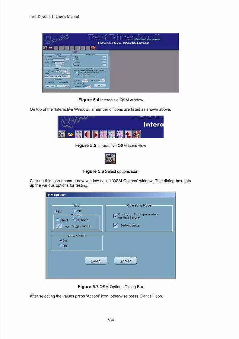
8/3/2019 V200UserManual
http://slidepdf.com/reader/full/v200usermanual 68/171
Test Director II User’s Manual
V-4
Figure 5.4 Interactive QSM window
On top of the ‘Interactive Window’, a number of icons are listed as shown above.
Figure 5.5 Interactive QSM icons view
Figure 5.6 Select options icon
Clicking this icon opens a new window called ‘QSM Options‘ window. This dialog box setsup the various options for testing.
Figure 5.7 QSM Options Dialog Box
After selecting the values press ‘Accept’ icon, otherwise press ‘Cancel’ icon.

8/3/2019 V200UserManual
http://slidepdf.com/reader/full/v200usermanual 69/171
Interactive QSM
V-5
Dialog box options
Log
When the log is on, the test results are all logged into a file.
Format
The log can be displayed in either of the two formats, namely Short and Verbose. When theoption short is selected, the contents of the log file are given in short. When the optionverbose is selected, the contents of the log file are in detail. When the log is off, the testresults are not logged into the file. In the Short mode only failure analysis reports and theDevice / Board Pass or Fail status will be reported. In Verbose apart from the analysisreport, each pin failure report is included in the Log.
DRC check
When this option is On then the DRC check is performed.
V.4 Operating Mode
During UUT compare Stop on first failure
\When comparing the Traces the process will be stopped if any failure observed during theoperation. This will stop testing further and other pins and links.This will be used for reliability check and confirm of similarity of device connectivity in theBoard.
Detect Links
Checking this option will confirm the Links obtained in regular probing of Pins. Linkconfirmation shall be selected / deselected in Learn Mode. The same thing will apply toVerify and Test mode, where the mode at Learnt is followed.
Link confirmation will be useful to avoid terming as short, any Low impedance point such asbetween Power Points or in case of reactive impedance loads.
The UUT Learn function is a very useful feature provided in the interactive QSM mode. Thisfeature is especially useful to test individual devices, because the complete testing of thedevice including tracing links, detecting shorts or opens, tracing the nodal characteristicsetc. are done in one shot.
Clicking the UUT Learn button start learning the device under test for all the above
mentioned characteristics for all the pins of the device and the Reference pin can bechanged and relearned for the check.
Click on UUT Learn button
Click this button to proceed further. It scans the device for open pins and the links presentwithin the device. The open and short pins are displayed in the result box and the links /HIZ are displayed in the clip window.
The UUT Compare function is useful in comparing devices for the learnt signatures.instantaneously. The characteristics of a good device learnt and tested with that of thesuspected device being trouble-shooted.

8/3/2019 V200UserManual
http://slidepdf.com/reader/full/v200usermanual 70/171
Test Director II User’s Manual
V-6
Figure 5.8 Device Compare connect Info Dialog Box
Connectivity
The same device can be compared against the previous learnt data
Online comparison
Using two clips the device data can be compared
Comparison Options
Mode Linear Non Linear Error %
Trace Comparison Tolerance
Enter the % of tolerance (in the Device Compare mode) whether the comparison is doneallowing some % tolerance.
V.5 QSM –VI Interactive window
The interactive window lists device info, Characteristics info, connection info, trace view anddual trace.
Figure 5.9 QSM Interactive Window

8/3/2019 V200UserManual
http://slidepdf.com/reader/full/v200usermanual 71/171
Interactive QSM
V-7
UUT Info
Enter library, device name, total pins, Pin Number and reference Pin values.
Figure 5.10 Device Info
Known or Unknown
Known represents the devices available in Library for quick reference. Unknowndevices are those unavailable in Library or not identified for the base number of thedevice. Appropriate device selection can be made for correct results.
Device Name
Specify the name of the device that is to be tested.
Test Points
Enter the total number of pins for the device you are about to test. You can vary thetotal pins using the increment / decrement buttons. If the Device entered is found inlibrary, the system will automatically enter the Total Pins while starting Interactive
or other UUT Learn and compare modes.
Patterns
Default Qmax patterns which are generated and calibrated will be loaded for easyselection of available patterns for testing.If user wants to create new patterns he/she can select New button and follow thefurther screen menus.
New button selection will open pattern pop up menu for selecting any pattern andname the pattern as the user desires. After this select the Number of cycles andother selective parameter as shown in the figure which is explained below:
Figure 5.11 Patterns window

8/3/2019 V200UserManual
http://slidepdf.com/reader/full/v200usermanual 72/171
Test Director II User’s Manual
V-8
Figure 5.12 Waveform Details pop up menu
Enter the pattern name. If you want to change the name or delete the pattern, press‘Delete Pattern’ icon.
Choose the amplitude, source impedance and time per tick values given in the individualbuttons and select ‘Next’. Otherwise click on ‘Abort’ icon to enter a new pattern name andfresh set of values.
On clicking the ‘Next’ icon, a new window called ‘Define waveform’ window opens.
Figure 5.13 Define Waveform Window
In this window, you get Pattern type, Ticks per cycle, Cycles, Drive time, Amplitude.
To select multiple patterns hold down the Ctrl key.
Clicking on the Add button opens a new window called ‘Define Patterns’.

8/3/2019 V200UserManual
http://slidepdf.com/reader/full/v200usermanual 73/171
Interactive QSM
V-9
Figure 5.14Define Patterns Pop up menu
Enter the values for ticks per cycle and number of cycles.
Mention the polarity whether ‘Unipolar or Bipolar’.
Enter the Amplitude value.
Select the waveform type
Figure 5.15 Waveform Type selection window
After selecting the values for Ticks per cycle, Number of cycles, Polarity, Amplitude andwaveform type, Click on ‘Apply’ icon. If you would like to enter different set of values andwaveform type, click on ‘Cancel icon.
Click on ‘Preview’ icon to preview the waveform pattern whether it is Mathematical (sin, cos,tan) Square, Triangle, Ramp or DC as defined so far in defining new pattern.

8/3/2019 V200UserManual
http://slidepdf.com/reader/full/v200usermanual 74/171
Test Director II User’s Manual
V-10
Figure 5.16 Pattern Preview for the selected Waveform Definition
Click on ‘Previous’ icon in the ‘Define Waveform’ window to go back to the waveform detailswindow.
Press the ‘Apply’ icon after entering the relevant values and after previewing the waveform.You will be prompted by the question asking you to save the current pattern as the User Defined Pattern. Click Yes if you want to save the parameters in a folder; otherwise click No
Connectivity
Select the Clip type, Probe type, fixture sub-window.
Select the Probe& Ref channels by the drop down button
Figure 5.17 Device Connectivity window
Clip 1Selecting Clip1 makes the mode of testing to be clip and selects Clip1 for testing. Systemsupports two clip definitions.
Clip 2Selecting Clip2 makes the mode of testing to be clip and selects Clip2 for testing.
FixtureSelect this button to make the mode of testing to be fixture.
Probe(s)
Probe1 & Ref1Selecting Probe1&Ref1 makes the mode of testing to be Probe and selects the flying probe
as PROBE1 with Ref1.

8/3/2019 V200UserManual
http://slidepdf.com/reader/full/v200usermanual 75/171
Interactive QSM
V-11
Probe 2 & Ref2Selecting Probe2&Ref2 makes the mode of testing to be Probe and selects the flying probeas PROBE2 with Ref2.
After entering the relevant values required for testing the board, press the ‘Start’ button.
Figure 5.18 Interactive mode menu window
Online Comparison (Dual Trace Mode)
This Interactive mode is provided to see the dual trace for comparing two similar devices onBoard. To view the traces for both the devices Both the Clips or Both Probes modes is tobe selected.
Checking the Dual Trace mode, two boards can be tested simultaneously and the tracescompared. This is done by testing the trace with two probes i.e. probe 1 with respect tofixed reference 1 and probe 2 with respect to fixed reference 2. This mode would be usefulin fast diagnosis of two similar boards without storing the traces.
When this option is checked, the other modes are disabled.
If Probe is selected, you should use both Probe1 and Probe2. In Clip mode, the systemtakes trace from Clip1 and Clip2.
Fixture is not allowed in Dual Trace Mode.
Trace Mode
Select ‘trace Mode’ whether VI, VT OR VZ.
Figure 5.19 Trace Mode select Box
Select whether ‘Dual trace’ is required or not.
Trace Modes
V-ISelecting V-I, displays the waveform as Voltage plotted against Current. The display typecan be changed while performing the test.

8/3/2019 V200UserManual
http://slidepdf.com/reader/full/v200usermanual 76/171

8/3/2019 V200UserManual
http://slidepdf.com/reader/full/v200usermanual 77/171
Interactive QSM
V-13
9. Check the Show Trace option, to show each and every trace.
10. The pin is tested with respect to the reference pin that is set. In the interactivemode, the device is learnt with fixed reference only.
11. Click the Stop Interactive button, to stop learning the trace interactively.
12. To store a trace, click the Store button. You can store as many as 4 traces. Once atrace has been stored, you cannot change the comparison type (linear, non-linear or error%). This is enabled again, only when all the stored traces are removed.
13. To remove the stored trace, click the Remove button. The total number of tracesstored are also displayed
14. Once the device is tested, the result is displayed in the interactive window.
15. To quit the interactive mode, click the button Close.
Summary
This chapter explained the use of QSM traces usage and how to use effectively totroubleshoot the PCB. The use of various options for different applications also explainedin a clear manner.

8/3/2019 V200UserManual
http://slidepdf.com/reader/full/v200usermanual 78/171
Test Director II User’s Manual
V-14

8/3/2019 V200UserManual
http://slidepdf.com/reader/full/v200usermanual 79/171
Chapter VI Measurements

8/3/2019 V200UserManual
http://slidepdf.com/reader/full/v200usermanual 80/171
Test Director II User’s Manual Vol1
VI.2
Introduction
This chapter describes the details of the procedures used to measure parameters such asResistance(R), Capacitance(C), Voltage (V), Inductance (L), and Frequency (F) in theInteractive Workstation Window, using this tester.
VI.1 How to: Starting the Measurement Parameters
1. To start the measurements of parameters like resistance, capacitance,inductance, click on the Start button, and point to Programs. (Figure 6.1)
2. Click on the programs folder. This will open the available programs in thesystem. Select Qmax under which TestDirector suite is available and thenclick on the Interactive Application icon in the TestDirector II sub-folder.The Interactive Application window opens. (Figure 6.2)
3. After opening the Interactive Application window, click on the buttons of the
parameters like resistance, capacitance, inductance which you would liketo measure, in the Interactive Application window.
Figure 6.1 Opening the Interactive Workstation Window
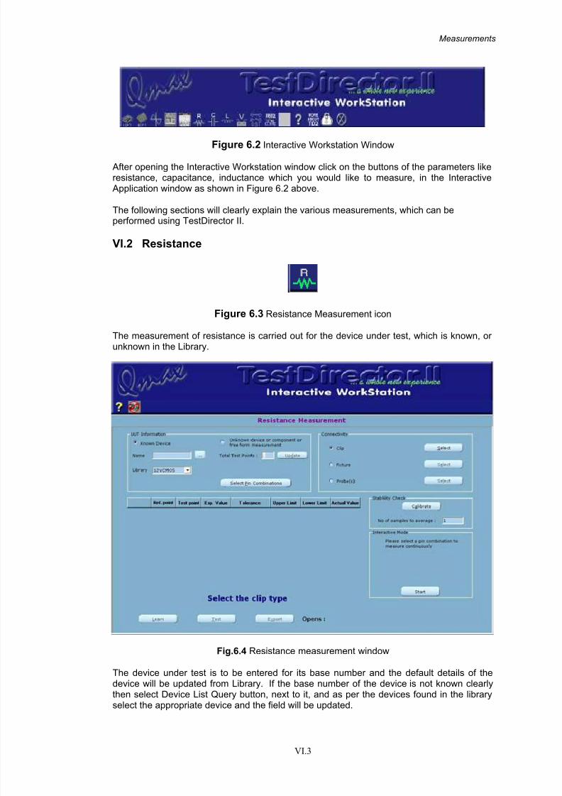
8/3/2019 V200UserManual
http://slidepdf.com/reader/full/v200usermanual 81/171
Measurements
VI.3
Figure 6.2 Interactive Workstation Window
After opening the Interactive Workstation window click on the buttons of the parameters likeresistance, capacitance, inductance which you would like to measure, in the InteractiveApplication window as shown in Figure 6.2 above.
The following sections will clearly explain the various measurements, which can beperformed using TestDirector II.
VI.2 Resistance
Figure 6.3 Resistance Measurement icon
The measurement of resistance is carried out for the device under test, which is known, or unknown in the Library.
Fig.6.4 Resistance measurement window
The device under test is to be entered for its base number and the default details of thedevice will be updated from Library. If the base number of the device is not known clearly
then select Device List Query button, next to it, and as per the devices found in the libraryselect the appropriate device and the field will be updated.
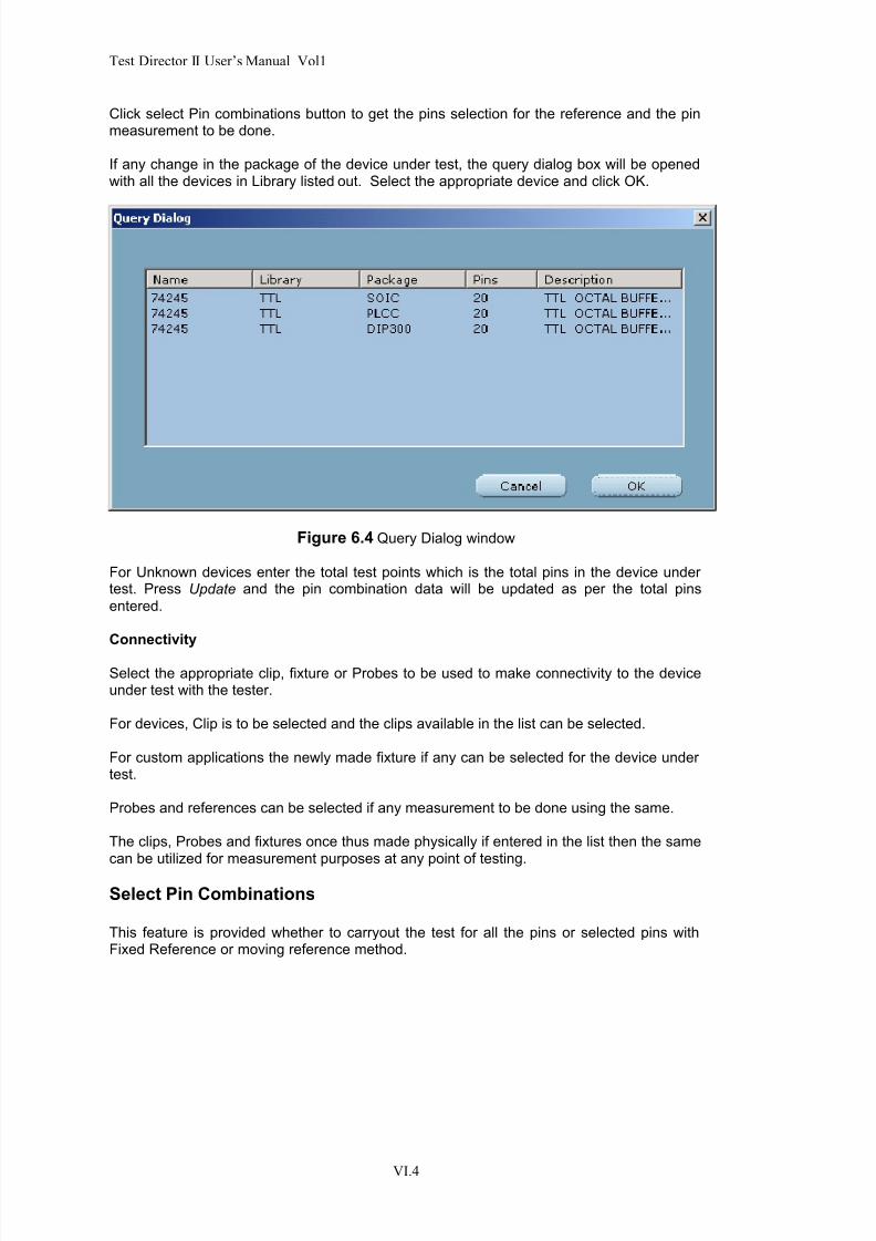
8/3/2019 V200UserManual
http://slidepdf.com/reader/full/v200usermanual 82/171
Test Director II User’s Manual Vol1
VI.4
Click select Pin combinations button to get the pins selection for the reference and the pinmeasurement to be done.
If any change in the package of the device under test, the query dialog box will be openedwith all the devices in Library listed out. Select the appropriate device and click OK.
Figure 6.4 Query Dialog window
For Unknown devices enter the total test points which is the total pins in the device under test. Press Update and the pin combination data will be updated as per the total pins
entered.
Connectivity
Select the appropriate clip, fixture or Probes to be used to make connectivity to the deviceunder test with the tester.
For devices, Clip is to be selected and the clips available in the list can be selected.
For custom applications the newly made fixture if any can be selected for the device under test.
Probes and references can be selected if any measurement to be done using the same.
The clips, Probes and fixtures once thus made physically if entered in the list then the samecan be utilized for measurement purposes at any point of testing.
Select Pin Combinations
This feature is provided whether to carryout the test for all the pins or selected pins withFixed Reference or moving reference method.

8/3/2019 V200UserManual
http://slidepdf.com/reader/full/v200usermanual 83/171
Measurements
VI.5
Figure 6.5 Select pin combination window
Fixed Reference
Select the pin which is reference and the values are measured with respect to this pin only.
Moving reference
Moving reference pin is for checking the values from the reference pin to other pins in theforward direction or with cross-reference.
Select the appropriate reference pin and types of combination for which the value is to bemeasured.
Choosing the correct pin combinations click OK.
The test points and ref points will be updated and the tester is now ready to measure thevalues.
Learn
Click Learn button to start learning all the pin combinations selected and the values will bedisplayed in the Exp Value column.
On checking multiple times the Tolerance can be set in to have the error of approximationfor the learnt value .
The Set tolerance pop up window is illustrated below.
Select the tolerance Information for the device under test as required and enter thetolerance required in percentage, Envelope value min-max, or range within values.
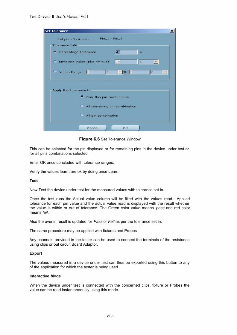
8/3/2019 V200UserManual
http://slidepdf.com/reader/full/v200usermanual 84/171
Test Director II User’s Manual Vol1
VI.6
Figure 6.6 Set Tolerance Window
This can be selected for the pin displayed or for remaining pins in the device under test or for all pins combinations selected.
Enter OK once concluded with tolerance ranges.
Verify the values learnt are ok by doing once Learn.
Test
Now Test the device under test for the measured values with tolerance set in.
Once the test runs the Actual value column will be filled with the values read. Appliedtolerance for each pin value and the actual value read is displayed with the result whether the value is within or out of tolerance. The Green color value means pass and red color means fail.
Also the overall result is updated for Pass or Fail as per the tolerance set in.
The same procedure may be applied with fixtures and Probes
Any channels provided in the tester can be used to connect the terminals of the resistanceusing clips or out circuit Board Adaptor.
Export
The values measured in a device under test can thus be exported using this button to anyof the application for which the tester is being used .
Interactive Mode
When the device under test is connected with the concerned clips, fixture or Probes thevalue can be read instantaneously using this mode.

8/3/2019 V200UserManual
http://slidepdf.com/reader/full/v200usermanual 85/171
Measurements
VI.7
The Selected pin combination displayed with double arrow in the screen will be measuredand displayed its current value for reference.
The value displayed may be cross checked with the value in the actual column for the learntand tested value.
Whenever the start button is clicked, the instantaneous value of resistance across theterminals of probe and reference is measured and displayed.
Figure 6.7 Resistance measurement
StartClick on the “Start” button to measure the resistance. The instantaneous value obtained willbe displayed.
StopStop button is to be used as soon as the measurement is over. This brings an end to themeasurement operation using the tester.
Stability Check
CalibrateThis button is provided for calibrating the measurement before measuring any unknownvalue.
In resistance measurement the calibrate button is provided to do calibration if required.Normally, this is performed before learning any values and the calibration provides anyundue errors in the initial set value will be corrected.
Automatic calibration menu will be displayed if any change in the reference value is morethen the limit.
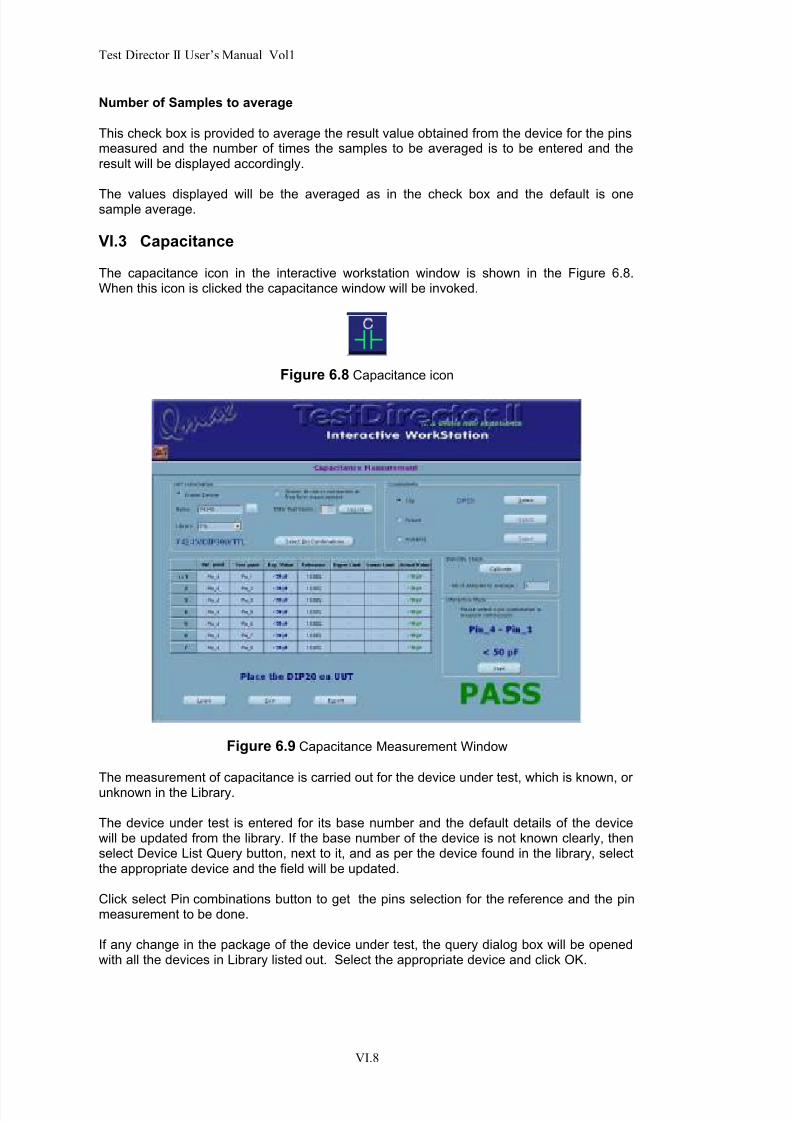
8/3/2019 V200UserManual
http://slidepdf.com/reader/full/v200usermanual 86/171
Test Director II User’s Manual Vol1
VI.8
Number of Samples to average
This check box is provided to average the result value obtained from the device for the pinsmeasured and the number of times the samples to be averaged is to be entered and theresult will be displayed accordingly.
The values displayed will be the averaged as in the check box and the default is onesample average.
VI.3 Capacitance
The capacitance icon in the interactive workstation window is shown in the Figure 6.8.When this icon is clicked the capacitance window will be invoked.
Figure 6.8 Capacitance icon
Figure 6.9 Capacitance Measurement Window
The measurement of capacitance is carried out for the device under test, which is known, or unknown in the Library.
The device under test is entered for its base number and the default details of the devicewill be updated from the library. If the base number of the device is not known clearly, thenselect Device List Query button, next to it, and as per the device found in the library, selectthe appropriate device and the field will be updated.
Click select Pin combinations button to get the pins selection for the reference and the pinmeasurement to be done.
If any change in the package of the device under test, the query dialog box will be openedwith all the devices in Library listed out. Select the appropriate device and click OK.

8/3/2019 V200UserManual
http://slidepdf.com/reader/full/v200usermanual 87/171
Measurements
VI.9
Figure 6.10 Query Dialog window
For Unknown devices enter the total test points which is the total pins in the device under test. Press Update and the pin combination data will be updated as per the total pins
entered.
Connectivity
Select the appropriate clip, fixture or Probes to be used to make connectivity to the deviceunder test with the tester.
For devices Clip is to be selected and the clips available in the list can be selected.
For custom applications the newly made fixture if any can be selected for the device under test.
Probes and references can be selected if any measurement to be done using the same.
The clips , Probes and fixtures once thus made physically if entered in the list , then thesame can be utilized for measurement purposes at any point of testing.
Select Pin Combinations
This feature is provided whether to carryout the test for all the pins or selected pins withFixed Reference or moving reference method.
Fixed Reference
Select the pin which is the reference and the values are measured with respect to this pinonly.
Moving reference
Moving reference pin is for checking the values from the reference pin to other pins in theforward direction or with cross-reference.
Select the appropriate reference pin and types of combination for which the value is to bemeasured.
Choosing the correct pin combinations click OK.
The test points and ref points will be updated and the tester is now ready to measure thevalues.

8/3/2019 V200UserManual
http://slidepdf.com/reader/full/v200usermanual 88/171
Test Director II User’s Manual Vol1
VI.10
Figure 6.11 Select pin combination windowLearn
Click Learn button to start learning all the pin combinations selected and the values will bedisplayed in the Exp Value column.
On checking multiple times, the Tolerance can be set in to have the error of approximationfor the learnt value .
The Set tolerance pop up window is illustrated below.
Figure 6.12 Set Tolerance Window

8/3/2019 V200UserManual
http://slidepdf.com/reader/full/v200usermanual 89/171
Measurements
VI.11
Select the tolerance Information for the device under test as required and enter thetolerance required in percentage, Envelope value min-max, or range within values.
This can be selected for the pin displayed or for remaining pins in the device under test or for all pins combinations selected.
Enter OK once concluded with tolerance ranges.
Verify the values learnt are ok by doing once Learn.
Test
Now Test the device under test for the measured values with tolerance set in.
Once the test runs the Actual value column will be filled with the values read. Appliedtolerance for each pin value and the actual value read is displayed with the result whether the value is within or out of tolerance. The Green color value means the pass and red color
means fail.
Also the overall result is updated for Pass or Fail as per the tolerance set in.
The same procedure may be applied with fixtures and Probes
Any channels provided in the tester can be used to connect the terminals of thecapacitance using clips or Out Circuit Board Adaptor.
Export
The values measured in a device under test can thus be exported using this button to anyof the application for which the tester is being used.
Interactive Mode
When the device under test is connected with the concerned clips, fixture or Probes thevalue can be read instantaneously using this mode .
The Selected pin combination displayed with double arrow in the screen will be measuredand displayed its current value for reference.
The value displayed may be crosschecked with the value in the actual column for the learntand tested value.
Whenever the start button is clicked, the instantaneous value of resistance across the
terminals of probe and reference selected, is measured and displayed.
Start
Click on the “Start” button to measure the resistance. The instantaneous value obtained willbe displayed.
Stop
Stop button is to be used as soon as the measurement is over. This brings an end to themeasurement operation using the tester.

8/3/2019 V200UserManual
http://slidepdf.com/reader/full/v200usermanual 90/171
Test Director II User’s Manual Vol1
VI.12
Stability CheckCalibrate
This button is provided for calibrating the measurement before measuring any unknownvalue.
In Capacitance measurement the calibrate button is provided to do calibration if required
Normally, this is performed before learning any values and the calibration provides anyundue errors in the initial set value will be corrected
Automatic calibration menu will be displayed if any change in the reference value is morethen the limit. You need not do any calibration at the time of testing.
Number of Samples to average
This check box is provided to average the result value obtained from the device for the pinsmeasured and the number of times the samples to be averaged is to be entered and the
result will be displayed accordingly.
The values displayed will be the averaged as in the check box and the default is onesample average.
VI.4 Voltage
The Voltage icon in the interactive workstation is shown in the Figure. The measuredvoltage is displayed using the unit volts.
To measure DC voltages while testing a PCB or any other electronic circuitry, this feature isprovided. Voltages upto 25 volts maximum can be measured.
In the Interactive WorkStation window, select the voltage (V) icon for measuring thevoltage. The voltage measurement window opens as shown below in figure
Figure 6.13 Voltage icon in Interactive Workstation window
The measurement of voltage is carried out for the device under test pins which is known or unknown in the Library.
The device under test is entered for its base number and the software automaticallysearches for the presences of this number in the library and updates the field.
Click select Pin combinations button to get automatic search of the device in the Library.
If any change in the package the query dialog box will be opened with all the devices inLibrary listed out. Select the appropriate device and click OK.
For Unknown devices enter the total test points which is the total pins in the device under test.

8/3/2019 V200UserManual
http://slidepdf.com/reader/full/v200usermanual 91/171
Measurements
VI.13
Figure 6.14 Query Dialog window
Press Update the Select pin combination data will be updated as per the total pins entered.
Connectivity
Select the appropriate clip, fixture or Probes to be used to make connectivity to the deviceunder test with the tester.
For devices, Clip is to be selected and the clips available in the list can be selected.
For custom applications the newly made fixture if any can be selected for the device under test.
Probes and references can be selected if any measurement to be done using the same.
The clips, Probes and fixtures once thus made physically if entered in the list then thesame can be utilized for measurement purposes at any point of testing.
Select Pin Combinations
This feature is provided whether to carryout the test for all the pins or selected pins withFixed Reference or moving reference method.
Figure 6.15 Select pin combination window
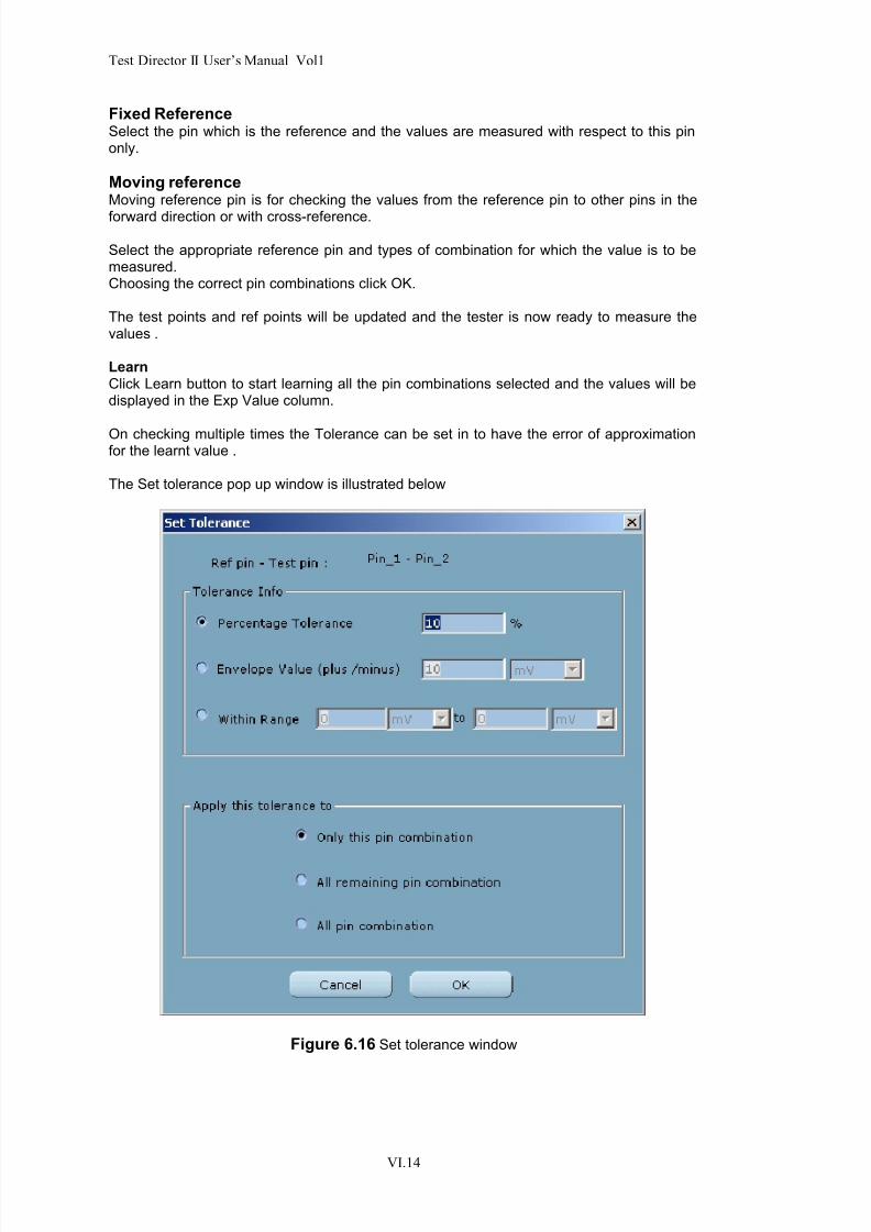
8/3/2019 V200UserManual
http://slidepdf.com/reader/full/v200usermanual 92/171
Test Director II User’s Manual Vol1
VI.14
Fixed ReferenceSelect the pin which is the reference and the values are measured with respect to this pinonly.
Moving referenceMoving reference pin is for checking the values from the reference pin to other pins in the
forward direction or with cross-reference.
Select the appropriate reference pin and types of combination for which the value is to bemeasured.Choosing the correct pin combinations click OK.
The test points and ref points will be updated and the tester is now ready to measure thevalues .
LearnClick Learn button to start learning all the pin combinations selected and the values will bedisplayed in the Exp Value column.
On checking multiple times the Tolerance can be set in to have the error of approximationfor the learnt value .
The Set tolerance pop up window is illustrated below
Figure 6.16 Set tolerance window
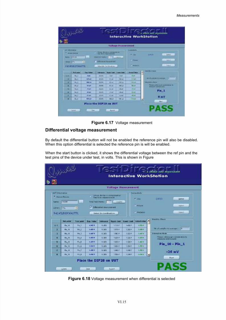
8/3/2019 V200UserManual
http://slidepdf.com/reader/full/v200usermanual 93/171
Measurements
VI.15
Figure 6.17 Voltage measurement
Differential voltage measurement
By default the differential button will not be enabled the reference pin will also be disabled.When this option differential is selected the reference pin is will be enabled.
When the start button is clicked, it shows the differential voltage between the ref pin and thetest pins of the device under test, in volts. This is shown in Figure
Figure 6.18 Voltage measurement when differential is selected

8/3/2019 V200UserManual
http://slidepdf.com/reader/full/v200usermanual 94/171
Test Director II User’s Manual Vol1
VI.16
VI.5 Inductance
The inductance icon is shown in the Figure 6.13. When the inductance icon in theInteractive Workstation window (Figure 6.14) is clicked the inductance window opens.
Figure 6.19 Inductance icon
Figure 6.20 Inductance Measurement window
The measurement of inductance is carried out for the device under test, which is known, or unknown in the Library.
The device under test is entered for its base number and the default details of the devicewill be updated from library. If the base number of the device is not known clearly, thenselect Device List Query button, next to it, and as per the devices found in the library, selectthe appropriate device and the field will be updated.
Click select Pin combinations button to get automatic search of the device in the Library.
If any change in the package the query dialog box will be opened with all the devices inLibrary listed out. Select the appropriate device and click OK.

8/3/2019 V200UserManual
http://slidepdf.com/reader/full/v200usermanual 95/171
Measurements
VI.17
Figure 6.21 Query Dialog window
For Unknown devices enter the total test points which is the total pins in the device under test.
Press Update and the pin combination data will be updated as per the total pins entered.
Connectivity
Select the appropriate clip, fixture or Probes to be used to make connectivity to the deviceunder test with the tester.
For devices Clip is to be selected and the clips available in the list can be selected.
For custom applications the newly made fixture if any can be selected for the device under test.
Probes and references can be selected if any measurement to be done using the same.
The clips, Probes and fixtures once thus made physically if entered in the list then thesame can be utilized for measurement purposes at any point of testing.
Select Pin Combinations
This feature is provided whether to carryout the test for all the pins or selected pins withFixed Reference or moving reference method.
Figure 6.22 Select pin combination window

8/3/2019 V200UserManual
http://slidepdf.com/reader/full/v200usermanual 96/171
Test Director II User’s Manual Vol1
VI.18
Fixed ReferenceSelect the pin which is the reference and the values are measured with respect to this pinonly.
Moving referenceMoving reference pin is for checking the values from the reference pin to other pins in the
forward direction or with cross reference .
Select the appropriate reference pin and types of combination for which the value is to bemeasured.
Choosing the correct pin combinations click OK.
The test points and ref points will be updated and the tester is now ready to measure thevalues .
Learn
Click Learn button to start learning all the pin combinations selected and the values will be
displayed in the Exp Value column.
On checking multiple times the Tolerance can be set in to have the error of approximationfor the learnt value .
The Set tolerance pop up window is illustrated below.
Figure 6.23 Set tolerance window

8/3/2019 V200UserManual
http://slidepdf.com/reader/full/v200usermanual 97/171
Measurements
VI.19
Select the tolerance Information for the device under test as required and enter thetolerance required in percentage, Envelope value min-max, or range within values.
This can be selected for the pin displayed or for remaining pins in the device under test or for all pins combinations selected.
Enter OK once concluded with tolerance ranges.
Verify the values learnt are ok by doing once more Learn.
Test
Now Test the device under test for the measured values with tolerance set in
Once the test runs the Actual value column will be filled with the values read. Appliedtolerance for each pin value and the actual value read is displayed with the result whether the value is within or out of tolerance. The Green color value means the pass and red color means fail.
Also the overall result is updated for Pass or Fail as per the tolerance set in.
The same procedure may be applied with fixtures and probes
Any channels provided in the tester can be used to connect the terminals of the inductanceusing clips or Out circuit Board Adaptor
Interactive Mode
When the device under test is connected with the concerned clips, fixture or Probes thevalue can be read instantaneously using this mode .
The Selected pin combination displayed with double arrow in the screen will be measured
and displayed its current value for reference.
The value displayed may be cross checked with the value in the actual column for the learntand tested value.
Start
Click on the “Start” button to measure the inductance. The instantaneous value obtainedwill be displayed.
Stop
Stop button is to be used as soon as the measurement is over. This brings an end to themeasurement operation using the tester.
Stability Check
Calibrate
This button is provided for calibrating the measurement before measuring any unknownvalue.
In inductance measurement the calibrate button is provided to do calibration if required
Normally ,this is performed before learning any values and the calibration provides any
undue errors in the initial set value will be corrected

8/3/2019 V200UserManual
http://slidepdf.com/reader/full/v200usermanual 98/171
Test Director II User’s Manual Vol1
VI.20
Automatic calibration menu will be displayed if any change in the reference value is morethen the limit. You need not do any calibration at the time of testing
VI.6 Frequency
Figure 6.24 Frequency icon
The frequency icon in the Interactive Workstation window is shown above.
When this icon is clicked, the frequency measurement window appears and looks like asshown below in the Figure.
Frequency Jack
Check this box to enable the jack to be ready for Frequency measurement. Insert theProbe lead to attach with the Jack.
Figure 6.25 Frequency Options dialog box
The threshold range in volts is to be entered for measuring the frequency across theselected pin.

8/3/2019 V200UserManual
http://slidepdf.com/reader/full/v200usermanual 99/171
Measurements
VI.21
Figure 6.26 Frequency measurement
The measurement of frequency is carried out for the device under test, which is known, or unknown in the Library.
The device under test is entered for its base number and the software automaticallysearches for the presences of this number in the library and updates the field.
Click select Pin combinations button to get automatic search of the device in the Library.
If any change in the package the query dialog box will be opened with all the devices inLibrary listed out.
Select the appropriate device and click OK.
Figure 6.27 Query Dialog window
For Unknown devices enter the total test points which is the total pins in the device under test.
Press Update the Select pin combination and data will be updated as per the total pinsentered.
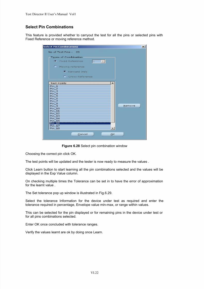
8/3/2019 V200UserManual
http://slidepdf.com/reader/full/v200usermanual 100/171
Test Director II User’s Manual Vol1
VI.22
Select Pin Combinations
This feature is provided whether to carryout the test for all the pins or selected pins withFixed Reference or moving reference method.
Figure 6.28 Select pin combination window
Choosing the correct pin click OK.
The test points will be updated and the tester is now ready to measure the values .
Click Learn button to start learning all the pin combinations selected and the values will bedisplayed in the Exp Value column.
On checking multiple times the Tolerance can be set in to have the error of approximationfor the learnt value .
The Set tolerance pop up window is illustrated in Fig.6.29.
Select the tolerance Information for the device under test as required and enter thetolerance required in percentage, Envelope value min-max, or range within values.
This can be selected for the pin displayed or for remaining pins in the device under test or for all pins combinations selected.
Enter OK once concluded with tolerance ranges.
Verify the values learnt are ok by doing once Learn.
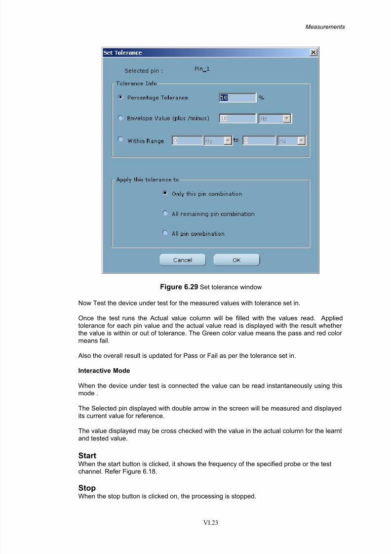
8/3/2019 V200UserManual
http://slidepdf.com/reader/full/v200usermanual 101/171
Measurements
VI.23
Figure 6.29 Set tolerance window
Now Test the device under test for the measured values with tolerance set in.
Once the test runs the Actual value column will be filled with the values read. Appliedtolerance for each pin value and the actual value read is displayed with the result whether the value is within or out of tolerance. The Green color value means the pass and red color means fail.
Also the overall result is updated for Pass or Fail as per the tolerance set in.
Interactive Mode
When the device under test is connected the value can be read instantaneously using thismode .
The Selected pin displayed with double arrow in the screen will be measured and displayedits current value for reference.
The value displayed may be cross checked with the value in the actual column for the learntand tested value.
StartWhen the start button is clicked, it shows the frequency of the specified probe or the testchannel. Refer Figure 6.18.
StopWhen the stop button is clicked on, the processing is stopped.

8/3/2019 V200UserManual
http://slidepdf.com/reader/full/v200usermanual 102/171
Test Director II User’s Manual Vol1
VI.24
Stability Check
Number of samples to be averaged can be entered and that many times the averaging willbe done and the value will be displayed for stable readings.
Note:
Frequency measurement value upto 48 MHz can be measured using this tester .
Summary
Thus, the method for measuring the Resistance, Capacitance, Voltage, Frequency andInductance has been explained briefly in this chapter.
8/3/2019 V200UserManual
http://slidepdf.com/reader/full/v200usermanual 103/171
Chapter VII Open/Short Test
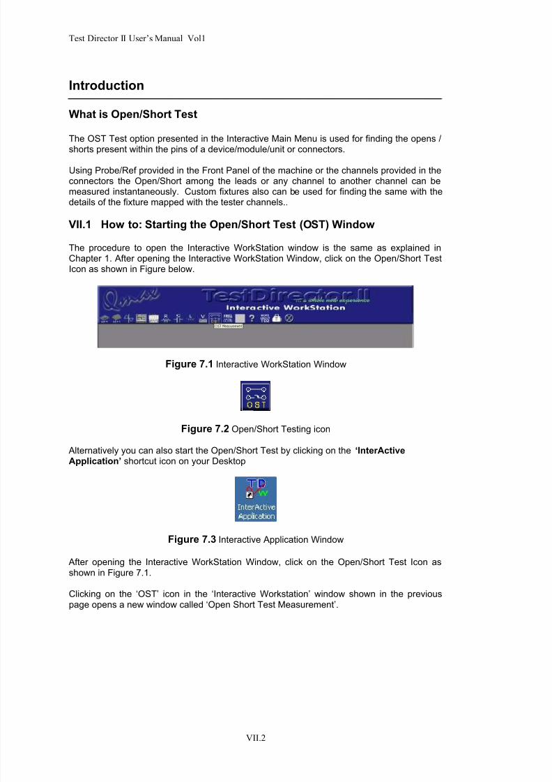
8/3/2019 V200UserManual
http://slidepdf.com/reader/full/v200usermanual 104/171
Test Director II User’s Manual Vol1
VII.2
Introduction
What is Open/Short Test
The OST Test option presented in the Interactive Main Menu is used for finding the opens /shorts present within the pins of a device/module/unit or connectors.
Using Probe/Ref provided in the Front Panel of the machine or the channels provided in theconnectors the Open/Short among the leads or any channel to another channel can bemeasured instantaneously. Custom fixtures also can be used for finding the same with thedetails of the fixture mapped with the tester channels..
VII.1 How to: Starting the Open/Short Test (OST) Window
The procedure to open the Interactive WorkStation window is the same as explained inChapter 1. After opening the Interactive WorkStation Window, click on the Open/Short TestIcon as shown in Figure below.
Figure 7.1 Interactive WorkStation Window
Figure 7.2 Open/Short Testing icon
Alternatively you can also start the Open/Short Test by clicking on the ‘InterActiveApplication’ shortcut icon on your Desktop
Figure 7.3 Interactive Application Window
After opening the Interactive WorkStation Window, click on the Open/Short Test Icon asshown in Figure 7.1.
Clicking on the ‘OST’ icon in the ‘Interactive Workstation’ window shown in the previouspage opens a new window called ‘Open Short Test Measurement’.

8/3/2019 V200UserManual
http://slidepdf.com/reader/full/v200usermanual 105/171
Open/Short Test
VII.3
VII.2 Description of the OST Measurement Window
Figure 7.4 OST Test Main screen
There are various test attributes provided as options in the interactive testing front-end
menu and the following sections briefly describe them.
Figure 7.5 Device Info
UUT Information
Known Device / Unknown DeviceThe device is to be selected for the identity. If the base number of the device is known,select Known Device otherwise select Unknown device. Known device selection will enablethe Library search for checking the availability of the device.
Device NameSpecify the name of the device that is to be tested.

8/3/2019 V200UserManual
http://slidepdf.com/reader/full/v200usermanual 106/171
Test Director II User’s Manual Vol1
VII.4
Device library Enter Device library or the software will automatically search for it from the available Librarywhen Select Pin combination is selected.
Unknown DeviceIf the device under test is not in the Library or the base number of the device is not known,this selection is to be made and enter the relevant details as required.
Total Test PinEnter the total number of pins for the device you are about to test.
Connectivity
Figure 7.6 Connectivity window
Select ClipThis button is provided to select the required clip for clipping the device on board.Any clip is to be selected from the List of clips available.
Select FixtureFixture is custom made to test any particular device or component on board as per therequirement. The pins are to be selected as the design of the fixture.
Select Probe(s)Select the probe and the reference points from Probe1& Ref1 or Probe 2&Ref
Select Pin CombinationsThis feature is provided whether to carryout the test for all the pins or selected pins withFixed Reference or moving reference method.
Figure 7.7 Select Pin Combination Window

8/3/2019 V200UserManual
http://slidepdf.com/reader/full/v200usermanual 107/171
Open/Short Test
VII.5
Fixed Reference
Select the pin which is the reference and the values are measured with respect to this pinonly.
Moving reference
Moving reference pin is for checking the values from the reference pin to other pins in theforward direction or with cross-reference.
Select the appropriate reference pin and types of combination for which the value is to bemeasured.
Choosing the correct pin combinations click OK.The test points and ref points will be updated and the tester is now ready to measure thevalues .
Click Learn button to start learning all the pin combinations selected and the values will bedisplayed in the Exp Value column.
Before starting learning the appropriate clips , fixtures or Probes should have been selectedand ready for learning.
VII.3 Drive Information for testing (OST parameters):
Figure 7.8 OST parameters Window Drive VoltageEnter the drive voltage value to be driven into all the pins of the device under test.
Voltage RangeSelect the voltage range from the drop down list of values. Select the nearby value for driving into the pins of the device. Ranges are 1V, 2.5V, 5V 8V & 13V.
Source ImpedanceSelect the source impedance through which the voltage selected to be driven into thedevice under test. Impedance ranges are 50 Ohms, 200 Ohms, 1Kohm, 10Kohm &100Kohms.

8/3/2019 V200UserManual
http://slidepdf.com/reader/full/v200usermanual 108/171
Test Director II User’s Manual Vol1
VII.6
Time Base
Select the time base the speed in which the Open Short test to be carried out Option for time base selection runs from 100nS to 200Micro Seconds in the steps of 100 nS.
Threshold
This is the resistance the user has to enter for checking the Open short between theselected Probe and Ref or Test channels selecting Clip1 or fixture. More than this value thesoftware will declare the returned value as Open.
Apply this value to
Selected pin combination
All Remaining pin combination
All pin combination
Once the selection is made enter OK.
Now the tester is ready to learn the Open Short among the pins displayed.
Click Learn and see the Exp value for all pin combinations selected.
Verify the values learnt are ok by doing once Learn.
Now Test the device under test for the measured values with drive info. set in.
Once the test runs the Actual value column will be filled with the values read. The Greencolor value means the pass and red color means fail.
Also the overall result is updated for Pass or Fail .
Interactive Mode
When the device under test is connected with the concerned clips, fixture or Probes thevalue can be read instantaneously using this mode .
The Selected pin combination displayed with double arrow in the screen will be measuredand displayed its current value for reference.
The value displayed may be cross checked with the value in the actual column for the learntand tested value.
StartClick on the “Start” button to measure the Open Short. The instantaneous value obtainedwill be displayed.
StopStop button is to be used as soon as the measurement is over. This brings an end to themeasurement operation using the tester.

8/3/2019 V200UserManual
http://slidepdf.com/reader/full/v200usermanual 109/171
Open/Short Test
VII.7
CalibrateThis button is provided for calibrating the measurement before measuring any unknownvalue.
In OST measurement the calibrate button is provided to do calibration if there are changesin the values and the stored reference value is changed. Automatic calibration menu will be
displayed if any change in the reference value is more then the limit. You need not do anycalibration at the time of testing.
Summary
This chapter clearly explained the usage of OST module application for the devices under test using the Open Short testing method.

8/3/2019 V200UserManual
http://slidepdf.com/reader/full/v200usermanual 110/171
Test Director II User’s Manual Vol1
VII.8

8/3/2019 V200UserManual
http://slidepdf.com/reader/full/v200usermanual 111/171
Chapter VIII Oscilloscope

8/3/2019 V200UserManual
http://slidepdf.com/reader/full/v200usermanual 112/171
Test Director II User’s Manual Vol1
VIII.2
Introduction
A brief overview of Digital Oscilloscopes
Digital oscilloscopes and waveform digitizers sample signals using a fast analog to digital
converter (ADC). At evenly spaced intervals, the ADC measures the voltage levels andstores the digitized value in high-speed dedicated memory. The shorter the intervals, thefaster the digitizing rates are, and hence higher signal frequency can be recorded.
As the resolution of the ADC is greater, there is more sensitivity to small voltage changes.The time taken to record the values increases with more memory.
With digital oscilloscopes having more memories, the benefits associated with these digitaloscilloscopes are many some of which are listed below:
No details are missed on the waveforms thanks to higher effective sampling rate. Permanent glitch capture without waveform distortion. Better time and frequency resolution.
VIII.1 Functional description
Qmax's Triple channel oscilloscope is a powerful high-resolution instrument for waveformanalysis. The instruments features 12 bit ADCs, 8k if non-volatile acquisition memory per channel and a highly sophisticated trigger system to capture signals including spikes andglitches.
Scope utility is provided with 0.5 to 2.5 V ranges and time-base of 4 microseconds to 8milli-Seconds in step of 4 microseconds ranges. There are facilities for capturing waveforms,and analysis is possible through cursor measurements.
Capturing of the expected waveforms is possible with powerful triggering facility. Single
mode is available to see the instant waveforms.
Main features
12-bit resolution 8K Memory per channel High Display quality Segmentable memories with trigger point stamps Dynamic source impedance selection User-friendly interface Three channels
Opening the Oscilloscope Window
The procedure to open the Interactive WorkStation window is the same as mentioned inChapter III.
Selection
The oscilloscope utility can be selected by clicking the ‘Oscilloscope’ icon in the Interactiveworkstation window.

8/3/2019 V200UserManual
http://slidepdf.com/reader/full/v200usermanual 113/171
Oscilloscope
VIII.3
Figure 8.1 Oscilloscope Icon
Oscilloscope Options
In the Oscilloscope dialog box the control options are set for the Scope Utility.
The controls settings like voltage, and offset specific to the voltage are set in the Channelsgroup box. In the Timebase+Trigger group box, the trigger condition, and trigger modes areset and the required timebase is selected. Descriptions of the control are as follows:
Figure 8.2 Oscilloscope Dialog Box
Channels
To set up the trigger condition like positive edge or negative edge, with respect to channel,the Trigger button is used.
Trace ON / OFFThis group helps in switching the channels. These button controls are toggling type with ONand OFF functionality.
Figure 8.3 Trace ON / OFF

8/3/2019 V200UserManual
http://slidepdf.com/reader/full/v200usermanual 114/171
Test Director II User’s Manual Vol1
VIII.4
Select ChannelMultiplexed control for channel settings. This select control sets the channel that isselected.
Figure 8.4 Select Channel buttons
Timebase+Trigger
The power of a digital oscilloscope in any given application depends on a combination of several features including the ability to trigger on the event of interest.
In oscilloscope, we can specify a channel for triggering along with trigger voltage andtrigger delay.
There are different modes of operation supported by the scope utility, which are as follows:
AutoAutomatically re-arms after each sweep. If no trigger occurs, one is generated at anappropriate rate.
NormalRe-arms after each sweep. If no trigger occurs after a reasonable length of time, themessage “No or Slow Trigger” is displayed.
SingleHolds display after a trigger occurs. Re-arms only when the Single button is pressed again.
StopStops the triggering. To restart, click Auto or Normal button.
Trigger To set up the trigger condition like positive edge or negative edge, with respect to channel,the Trigger button is used and trigger setup panel dialog will open.
Positive Edge TriggeringThe main objective of positive edge triggering is to lock the required transition (positivetransition) after you specify the delay. The trigger selection is shown in the screen as below:
Figure 8.5 Positive edge triggering
Negative Edge TriggeringThe main objective of negative edge triggering is to lock the required transition (negativetransition) after you specify the delay. The trigger selection screen is shown as in fig.8.6
Figure 8.6 Negative edge triggering

8/3/2019 V200UserManual
http://slidepdf.com/reader/full/v200usermanual 115/171
Oscilloscope
VIII.5
Figure 8.7 Trigger Setup
TimebaseSelect the time base for which processing is done
Figure 8.8 Time base
ImpedanceLoad impedance is given for the ranges 100K Ohms, 10K Ohms, 1K Ohms, 200 Ohms, 50
Ohms and Open source for easy selection.
Figure 8.9 Impedance
Volts/Division Selects the Volts/Division for which processing is done
Figure 8.10 Volts/Division
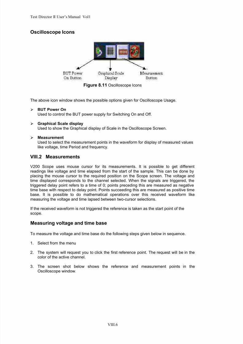
8/3/2019 V200UserManual
http://slidepdf.com/reader/full/v200usermanual 116/171
Test Director II User’s Manual Vol1
VIII.6
Oscilloscope Icons
Figure 8.11 Oscilloscope Icons
The above icon window shows the possible options given for Oscilloscope Usage.
BUT Power OnUsed to control the BUT power supply for Switching On and Off.
Graphical Scale displayUsed to show the Graphical display of Scale in the Oscilloscope Screen.
MeasurementUsed to select the measurement points in the waveform for display of measured valueslike voltage, time Period and frequency.
VIII.2 Measurements
V200 Scope uses mouse cursor for its measurements. It is possible to get differentreadings like voltage and time elapsed from the start of the sample. This can be done byplacing the mouse cursor to the required position on the Scope screen. The voltage and
time displayed corresponds to the channel selected. When the signals are triggered, thetriggered delay point refers to a time of 0; points preceding this are measured as negativetime base with respect to delay point. Points succeeding this are measured as positive timebase. It is possible to do mathematical operations over this received waveform likemeasuring the voltage and time lapsed between two-cursor selections.
If the received waveform is not triggered the reference is taken as the start point of thescope.
Measuring voltage and time base
To measure the voltage and time base do the following steps given below in sequence.
1. Select from the menu
2. The system will request you to click the first reference point. The request will be in thecolor of the active channel.
3. The screen shot below shows the reference and measurement points in theOscilloscope window.

8/3/2019 V200UserManual
http://slidepdf.com/reader/full/v200usermanual 117/171
Oscilloscope
VIII.7
Figure 8.12 Oscilloscope window Reference and Measurement Points
4. Now click the first reference point with your left mouse button once. Reference point will
be denoted as a ‘+’ in pink color.
5. After this, the system requests for the measurement point. Next left button click willdenote second reference point.
6. System displays the voltage difference and time base between measurement point andreference point with appropriate polarity in the same screen.

8/3/2019 V200UserManual
http://slidepdf.com/reader/full/v200usermanual 118/171
Test Director II User’s Manual Vol1
VIII.8

8/3/2019 V200UserManual
http://slidepdf.com/reader/full/v200usermanual 119/171
Chapter IX Function Generator

8/3/2019 V200UserManual
http://slidepdf.com/reader/full/v200usermanual 120/171
Test Director II User’s Manual Vol1
IX.2
Function Generator
IX.1 A brief description of Function Generator
Specification:
Sine, square, pulse, ramp DC and more 3 Channels with 20 MS/s 10 MHz wave outputs 12-bit, 64K-point deep arbitrary waveform generation User definable waveform patterns Easy portability Simple mouse click operation for measurements
V200 is designed to produce all the waveforms you need for the vast majority of electronicstest needs up to 10 MHz. Standard outputs include Sine, Cosine, Tan, square, ramp,Triangle, and other mathematical functional waveforms, dc volts and more.
When the testing of PCB requires arbitrary waveform for testing, this Function Generator simplifies the process of creating Arbitrary Waveforms and makes the measurements alsoeasy in on-screen display.
You can create an unlimited variety of unique waveforms that match your requirements andsuit your application purposes.
Additionally, the Graphical User Interface makes the Function Generator use easy.
The vast timebase range from 100 nS to 200 Micro Seconds with 100 nS steps makes theprocess of creating arbitrary waveforms easy on mouse click.
Custom Waveform Generation
Standard Waveforms are generated and stored for ready use.
You have to select the required pattern and drive the same into the PCB.
The patterns are depicted with Waveform type, amplitude, Source Impedance andfrequency for easy selection. The Library of waveforms comes ready with the tester.
Also you can generate any kind of waveform for custom requirements and store in thename you want and use it as required.
The software allows you to maintain a separate library for the patterns for future use.
The created patterns can be selected and used in any or all of the channels.
The waveforms can be created with a max. of 13V amplitude.
Preview screen is provided to see the generated waveform for one cycle.
Create the right waveform the first time, every time
The graphical color display, easy to use menus to help you create complex waveforms.User definable Library helps you to create the waveform for first time and every time. Thecreated waveforms can be used at any point of time.

8/3/2019 V200UserManual
http://slidepdf.com/reader/full/v200usermanual 121/171
Function Generator
IX.3
Follow the menus and enter the required parameters to set up your waveform, and thenverify the results with graph mode using preview screen.
Function Generator Window
The Function Generator feature helps to generate the user definable wave patterns or
Qmax Standard patterns to be selected and driven into the point where it is required.
The channels provided for this purpose are FC1, FC2 & FC3. The patterns can be editedalso and can be renamed for future use and reference.
The function Generator Icon is provided in the main window of Interactive Workstation. Onselecting this icon the Function Generator Main window opens. BUT, Grid show, MeasureIcon, and Close are the main buttons provided for the functions.
The channels FC1, FC2 and/or FC3 can be selected and the offset for each channel alsocan be set by dragging the offset cursor check box.
Volts per division for each selected channel also can be set. A separate check box is given.
Define wave pattern for each channel using Qmax Standard patterns or required functionalpattern can be defined by you and save in the user library.
The pattern can be selected and re-defined for each channel separately.
Mathematical functions like Sine, Cosine, Tan etc., can be selected just by using drop boxalongside Sine, Square, Triangle (Ramp) & DC waveforms can be selected by usingcheckbox provided for each.
The selected pattern can be previewed for correctness.
Once the selected waveform is correct the same can be stored in the name of User Librarynames and can be used for future reference.
Figure 9.1 Function Generator Icon in Interactive WorkStation window
IX.2 Opening the Qmax Function Generator
There are two ways you can open the Function Generator program in windowsenvironment.
You can select the Interactive Application program from your Programs menu and click theFunction Generator icon in the Interactive Application window.
Alternatively, you can double click the Interactive Application shortcut icon in your desktopand click the Function Generator icon in the Interactive WorkStation Application window.

8/3/2019 V200UserManual
http://slidepdf.com/reader/full/v200usermanual 122/171
Test Director II User’s Manual Vol1
IX.4
Figure 9.2 Function Generator Window
IX.3 Functional description
Channels
To set up the trigger condition like positive edge or negative edge, with respect to channel,the Trigger button is used.
Figure 9.3 Function Generator Channel Window
Trace ON / OFFThis group helps in switching the channels. These button controls are toggling type with ONand OFF functionality.
Figure 9.4 Trace ON / OFF

8/3/2019 V200UserManual
http://slidepdf.com/reader/full/v200usermanual 123/171
Function Generator
IX.5
Select ChannelMultiplexed control for channel settings. This select control sets the channel that isselected.
Figure 9.5 Select Channel
Function Generator Icons
Figure 9.6 Function Generator Icons
The above icon window shows the possible options given for Oscilloscope Usage.
BUT Power OnUsed to control the BUT power supply for Switching On and Off.
Graphical Scale display
Used to show the Graphical display of Scale in the Oscilloscope Screen.
MeasurementUsed to select the measurement points in the waveform for display of measured valueslike voltage, time Period and frequency.
Define Patterns
Figure 9.7 Define Patterns
This feature is provided to select the required waveform to be edited and used for drivinginto the respective point for the application.
Define Patterns button selection will open Waveform Details pop up menu for selecting anypattern from the Qmax patterns stored in the system. Else you can define new waveform
by the parameters given in the popup menu.

8/3/2019 V200UserManual
http://slidepdf.com/reader/full/v200usermanual 124/171
Test Director II User’s Manual Vol1
IX.6
You have to select the Amplitude, source Impedance and times per tick from their respective Drop box values.
Choose the amplitude, source impedance and time per tick values given in the individualdrop boxes and select 'Next'. Otherwise click on 'Abort' icon to enter a new pattern nameand fresh set of values.
Next it will take you to Define pattern with Ticks per cycle and number of cycles for thewaveform to be driven.
The polarity of the waveform to be driven is to be selected in the checkbox provided for Unipolar or Bipolar.
Now the amplitude of the waveform defined can be changed or edited if required or samevalue can be maintained.
It is now ready to select the waveform type to be defined.
IX.4 Measurement procedure
Function Generator uses mouse cursor for its measurements. It is possible to get differentreadings like Voltage and time elapsed from the start of the sample. Placing the mousecursor to the required position on the screen can do this. The voltage and time displayedcorresponds to the channel selected.
When the signals are triggered, the triggered delay point refers to a time of 0, pointspreceding this are measured as negative time base with respect to delay point. Pointssucceeding this are measured as positive time base. It is possible to do mathematicaloperations over this received waveform like measuring the voltage and time lapsedbetween two-cursor selections.
If the received waveform is not triggered the reference is taken as the start point of thescope.

8/3/2019 V200UserManual
http://slidepdf.com/reader/full/v200usermanual 125/171
Chapter X Boundary Scan Test

8/3/2019 V200UserManual
http://slidepdf.com/reader/full/v200usermanual 126/171
Test Director II User’s Manual Vol1
X.2
A Brief Introduction to Boundary Scan Test Concepts
Since its introduction as an industry standard in 1990, boundary-scan (also known asJTAG) has enjoyed growing popularity for board level manufacturing test applications.Boundary-scan has rapidly become the technology of choice for building reliable hightechnology electronic products with a high degree of testability. Due to the low-cost and IClevel access capabilities of boundary-scan, its use has expanded beyond traditional boardtest applications into product design and service.
X.1 What is Boundary Scan?
Boundary-scan, as defined by the IEEE Std. 1149.1 standard, is an integrated method for testing interconnects on printed circuit boards that are implemented at the IC level. Thiscapability enables in-circuit testing without the need of bed-of-nails and custom fixtures .
Why should I use Boundary Scan?
Recent marketing drive for reduced product size, such as portable phones and digitalcameras, higher functional integration, faster clock rates, shorter product life-cycle withdramatically faster time to market, has created new technology trends. These newtechnology trends include increased device complexity, fine pitch components such asSMTs and BGAs, increased IC-pin count, and smaller PCB traces.
This has created the following problems in product development:
Many boards include components that are assembled on both sides of the board.Most of the through-holes and traces are buried and inaccessible.
Loss of Physical Access to fine pitch components such as SMTs and BGAs makesit difficult to probe the pins and distinguish between manufacturing and designproblems.
When the In-Circuit- Tester (ICT) is not available and therefore manufacturingdefects cannot be easily detected and isolated.
Small-size products do not have test points, which make it difficult, or impossible toprobe suspected nodes.
High pin count devices and Flash devices (in BGA packages) are not socketed andare soldered directly to the board.
Every time an engineer selects a new processor or a different flash device, he hasto learn from scratch how to program the Flash memory
When a design includes CPLDs from different vendors, the engineer must usedifferent in-circuit programmers to program the CPLDs.
Boundary-scan technology is the only cost effective solution that can deal with the aboveproblems.
In the last few years, the number of devices that include boundary-scan has grownexponentially.
Almost every new microprocessor that is being introduced includes boundary-scan circuitryfor testing and in-circuit emulation. Most of the CPLDs and FPGAs manufacturers such asAltera, Lattice, and Xilinx, to mention a few, have incorporated boundary-scan logic intotheir components including additional circuitry that uses the boundary-scan 4-wire interfaceto program their devices in-system.
As the acceptance of boundary-scan as the main technology for interconnect testing andin-circuit programming has increased, the various boundary-scan test and in-systemprogramming tools have matured as well. The increased number of boundary-scan
components and mature boundary-scan tools provide engineers with the following benefits:

8/3/2019 V200UserManual
http://slidepdf.com/reader/full/v200usermanual 127/171
Boundary Scan Test
X.3
Easy to implement Design For Testability (DFT) Rules. Testability report prior to PCB layout enhances DFT. Find packaging problems prior to PCB layout. Little need for test points. No need for test fixtures. More control over the test process
Quickly diagnose (with high resolution) interconnect problems without writing anyfunctional test code.
Program code in flash devices. JTAG emulation and source-level debugging. Applying Boundary-Scan for Production Test
Production test is an obvious area in which the use of boundary-scan yields tremendousreturns.
Automatic test program generation and fault diagnostics using Boundary-Scan (JTAG)software products and the lack of expensive fixturing requirements can make the entire testprocess very economical. For products that contain edge connectors and digital interfacesthat are not visible from the boundary-scan chain, boundary-scan vendors offer a family of
boundary-scan controllable I/Os that provide a low cost alternative to expensive digital pinelectronics.
X.2 Requirements for Boundary Scan Test Data
The data required for generating a test of a UUT designed with boundary scan is verysimilar to that required for testing any other digital UUT.
There needs to be a physical description of the UUT in sufficient detail to support thegeneration of test patterns and the diagnosis of failures detected by those patterns. Thenthere is the definition of the test patterns themselves. Looking first at the physical design,there is the requirement for a description of all boundary scan devices on the UUT. Thisinformation is contained in the BSDL (Boundary Scan Description Language) model of eachdevice. BSDL models are typically available directly from the device vendor, or can beobtained from synthesis tools in the case of custom ASICs.
Boundary scan device chains are formed when the TDO lead of one boundary scan deviceis connected to the TDI lead of another. Chains can consist of several devices therebyforming a continuous path extending from the TDO lead of the first device to the TDI lead of the last device.
A critical requirement is that the positions of scan cells in the chain and their functionalitybe captured so that faulty circuit activity can be accurately diagnosed.
Test patterns serve two functions in a boundary scan test. Before any test can be applied,
the instruction register of the boundary scan device must be programmed to put the deviceinto the desired state, e.g., EXTEST, HIGHZ. Serial patterns representing the appropriateinstruction must be clocked into the device’s TDI port.
In addition to stimulus data, there is the requirement for expected response data, which isused to determine a go/no go condition, and provides valuable information for pin leveldiagnosis. The TDO output will be coming from LSB to MSB. Boundary scan test patternscan be expressed in many formats, but SVF (Serial Vector Format) is the most prevalent inthe industry. Test Patterns is defined in Serial Vector Format schema.

8/3/2019 V200UserManual
http://slidepdf.com/reader/full/v200usermanual 128/171
Test Director II User’s Manual Vol1
X.4
X.3 Procedure for Boundary Scan Test
Add the boundary scan devices present in the PCB in the scan path order.
Compile the BSD files in order to validate the input BSD files. Collect the BSD informationfor further testing.
It has been made fully automatic to identify the components in the PCB as Boundary Scandevices and the list of components will be added to the Board Database.
The BOM list and Net list entry is made to enter the same manually.
The files if similar to the one available in Library the type and package can be selected bythe Programmer.
The selected devices will be checked for any connectivity failure and Open Shorts duringLearn mode.
Once the learnt device data is from a Known Good Board the other PCBs can be compared
and the comparison should show Pass for the PCB under test.
Thus the testing in Boundary Scan Devices is made fully automatic and easy to follow up.
X.4 How To: Starting the Boundary Scan Test
Click on the ‘Inter Active Application’ icon on your Desktop
Open the ‘Interactive Workstation’ window.
On the top of the ‘Interactive Workstation’ window, click on ‘Boundary Scan Test’ icon.
Click on BST opens up the Configuration Popup to select the Boundary Scan file to test thechip on Board.
This menu is having BOM list and Net list of the PCB to be entered. If these are available infiles , the corresponding files may be open up.
The files of Boundary Scan devices in a PCB stored in the location can be included now inthe Detect Scan Path menu.
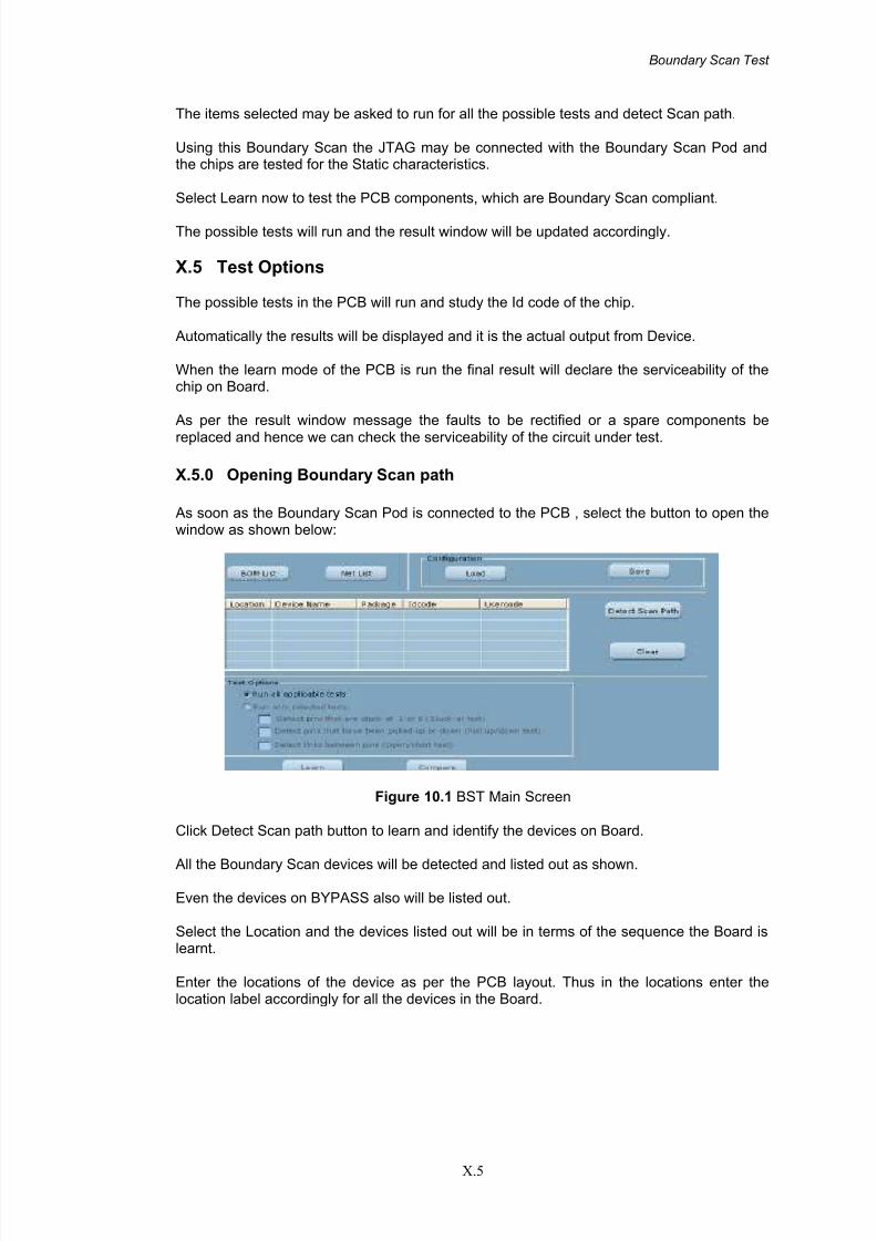
8/3/2019 V200UserManual
http://slidepdf.com/reader/full/v200usermanual 129/171
Boundary Scan Test
X.5
The items selected may be asked to run for all the possible tests and detect Scan path.
Using this Boundary Scan the JTAG may be connected with the Boundary Scan Pod andthe chips are tested for the Static characteristics.
Select Learn now to test the PCB components, which are Boundary Scan compliant.
The possible tests will run and the result window will be updated accordingly.
X.5 Test Options
The possible tests in the PCB will run and study the Id code of the chip.
Automatically the results will be displayed and it is the actual output from Device.
When the learn mode of the PCB is run the final result will declare the serviceability of thechip on Board.
As per the result window message the faults to be rectified or a spare components be
replaced and hence we can check the serviceability of the circuit under test.
X.5.0 Opening Boundary Scan path
As soon as the Boundary Scan Pod is connected to the PCB , select the button to open thewindow as shown below:
Figure 10.1 BST Main Screen
Click Detect Scan path button to learn and identify the devices on Board.
All the Boundary Scan devices will be detected and listed out as shown.
Even the devices on BYPASS also will be listed out.
Select the Location and the devices listed out will be in terms of the sequence the Board islearnt.
Enter the locations of the device as per the PCB layout. Thus in the locations enter thelocation label accordingly for all the devices in the Board.
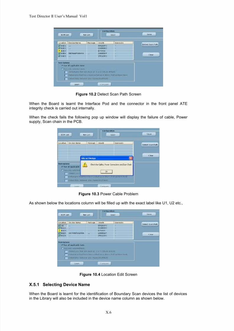
8/3/2019 V200UserManual
http://slidepdf.com/reader/full/v200usermanual 130/171
Test Director II User’s Manual Vol1
X.6
Figure 10.2 Detect Scan Path Screen
When the Board is learnt the Interface Pod and the connector in the front panel ATEintegrity check is carried out internally.
When the check fails the following pop up window will display the failure of cable, Power supply, Scan chain in the PCB.
Figure 10.3 Power Cable Problem
As shown below the locations column will be filled up with the exact label like U1, U2 etc.,
Figure 10.4 Location Edit Screen
X.5.1 Selecting Device Name
When the Board is learnt for the identification of Boundary Scan devices the list of devicesin the Library will also be included in the device name column as shown below.

8/3/2019 V200UserManual
http://slidepdf.com/reader/full/v200usermanual 131/171
Boundary Scan Test
X.7
Select the appropriate device on board.
Double click on the device column for each the BSDL file location will be popped up.
Select the correct file and open.
Figure 10.5 Selecting Device Name
Figure 10.6 Including BSDL files
The file-opening menu for the BSDL loaded in the system is shown above.
X.5.2 Selecting Package details
Though the device from the Board is studied there are other packages available in themarket for the same device number.
Hence select the proper device package, which is under test for learning the connectivity.
The dropped out list of packages available is as shown below:

8/3/2019 V200UserManual
http://slidepdf.com/reader/full/v200usermanual 132/171
Test Director II User’s Manual Vol1
X.8
Figure 10.7 Package Selecting
When the selection and entering the details for all the components studied is completedclick Load button so as to load the programs compiled using all the above entered devices.
The process of making the drive pattern is made fully automatic.
No process running can be seen in the front end.
As soon as the Load is pressed the file generated in the software will be ready to be driveninto the Board under test.
Figure 10.8 Window After Load is pressed
Once the program is ready select the Learn button to see the connectivity’s in the BoardUnder Test.
The Learnt data will be displayed with the Nets information and the Stuck at One and Zeronodes total number.
If the Net list of the Board Under Test is available the analysis can be done.

8/3/2019 V200UserManual
http://slidepdf.com/reader/full/v200usermanual 133/171
Boundary Scan Test
X.9
Figure 10.9 Learn Completed Screen
The list of Nets with the interconnectivity will be displayed and the details can be stored inthe database for further reference.
Figure 10.10 Result Window
Once the learnt data is correct then the same database will be used to compare for anynumber of boards.
When testing the Board click compare button and the result will be displayed in no time withthe list of Open/short Nodes in the PCB.

8/3/2019 V200UserManual
http://slidepdf.com/reader/full/v200usermanual 134/171
Test Director II User’s Manual Vol1
X.10
Figure 10.11 Comparison Passed Screen
X.5.3 BOM List entry
Bill of material of the Board under test is to be entered as shown below for any board.
One by one using the locations the device can be selected from the Library and the samewill be entered in the column.
Figure10.12 Empty BoM List Screen

8/3/2019 V200UserManual
http://slidepdf.com/reader/full/v200usermanual 135/171
Boundary Scan Test
X.11
Device List and the details are shown for the items in the library as shown below.
Figure 10.13 Device List Window
Some components entered in the BOM list and the sample is shown below.
Figure 10.14 Some Devices Entered in BoM List
X.5.4 Net List Details
Net list of the PCB components and their interconnectivity can be entered manually if thereis no Net List available for the PCB under development of test programs.
Net list for the components covered in the BOM details may be covered fully so as to takethe full coverage of components under test.The Net list including Power Pins is also entered to identify the Power Nets. Theinterconnectivity entered is summarized and displayed for ready reference.The entered Nets are marked with * mark and it can be selected for all the components or components wise.
Statistics window provides all the information entered through this interface. The Definednets can be renamed or net names can be given at any point of time for edit and use.
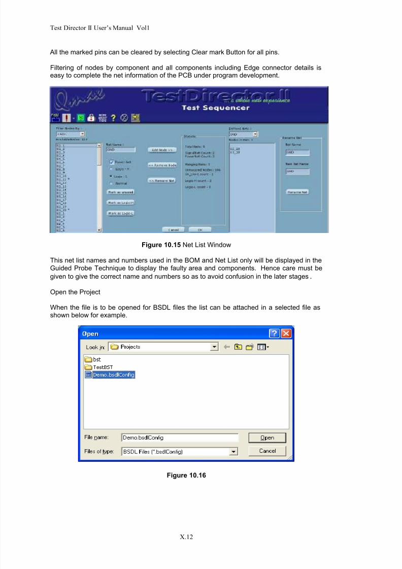
8/3/2019 V200UserManual
http://slidepdf.com/reader/full/v200usermanual 136/171
Test Director II User’s Manual Vol1
X.12
All the marked pins can be cleared by selecting Clear mark Button for all pins.
Filtering of nodes by component and all components including Edge connector details iseasy to complete the net information of the PCB under program development.
Figure 10.15 Net List Window
This net list names and numbers used in the BOM and Net List only will be displayed in theGuided Probe Technique to display the faulty area and components. Hence care must be
given to give the correct name and numbers so as to avoid confusion in the later stages.
Open the Project
When the file is to be opened for BSDL files the list can be attached in a selected file asshown below for example.
Figure 10.16

8/3/2019 V200UserManual
http://slidepdf.com/reader/full/v200usermanual 137/171
Boundary Scan Test
X.13
X.5.5 Saving the Learnt Database
Learnt database can be stored in the system under the same project where the files areavailable and the name of the files is also to be unique for quick reference.
A sample saving is shown below.
Figure 10.17
SummaryThe Boundary Scan test is done for the entire boundary scans chips on board using scanpath and the identification of faults in the chips is resulted.

8/3/2019 V200UserManual
http://slidepdf.com/reader/full/v200usermanual 138/171

8/3/2019 V200UserManual
http://slidepdf.com/reader/full/v200usermanual 139/171
Chapter XI Test Sequencer

8/3/2019 V200UserManual
http://slidepdf.com/reader/full/v200usermanual 140/171
Test Director II User’s Manual Vol1
XI.2
Test Sequencer
Introduction
Test Sequencer is used for sequencing of multiple tests with conditional branching,messaging, user prompting, external triggering and external handshake.
Board level testing using combination of ICFT, QSM-VI, Measurements, Card edge test,Boundary Scan Test etc., can be done in one test program through this Sequencer.
The main purpose of test Sequencer is to guide for effective sequencing of Operations tobe performed in the PCB/module to repair and rectify the fault at ease of use.
It has been simplified to greater extent to make the sequences through User Interface andhence the data entry is easy.
Test Sequencer is used to generate a sequence of tests such as:
Open/short Testing.
Device In-Circuit /Out-Circuit testing.
In-Circuit measurements for Inductance, Capacitance, Resistance, Voltage &Frequency.
Functional Testing of PCB/Module through Card Edge connectors.
Boundary Scan Testing of Boundary Scan compliant devices on Board.
User Prompting while repairing the Boards.
External Inputs, in port and out port facilities for easy transferability.
Delay in programming of execution for testing specific modules. Etc.,
One time sequencing of tests to be performed for Lifetime running on similar Boards for effective repair and maintenance.
Tagging of components in PCB and Schematic made through mouse click
Tagging of Layout for component identity through testing
Association of all documents like data files etc., in one folder for ease of reference
XI.1 How to: Starting the Test Sequencer
Opening the Test Sequencer Program
There are two ways you can open the Test Sequencer programs in windows environment.You can select the Test Sequencer program from your Programs menu. Or, you can
double click the Test Sequencer shortcut icon in your desktop.
To open the Test sequencer
1. To start the Test sequencer program, click on the Start button, and point to
Programs.

8/3/2019 V200UserManual
http://slidepdf.com/reader/full/v200usermanual 141/171
Test Sequencer
XI.3
2. Point to the folder named Qmax and then click on the Test Sequencer icon in theTest Director II sub-folder.
Figure 11- 1 Starting the Test Sequencer program window
3. Alternatively, to start the Test Sequencer program you can double-click on the Test
Sequencer icon shown below, on your desktop after installing the required QmaxTest Director II software.
Figure 11- 2 Test Sequencer Shortcut Icon
4. Click the Test Sequencer icon. The Test Sequencer window opens as shown inthe figure below.
Figure 11- 3 Test Sequencer Window

8/3/2019 V200UserManual
http://slidepdf.com/reader/full/v200usermanual 142/171
Test Director II User’s Manual Vol1
XI.4
5. Click on the Open button. A new sub-window called List of Programs opens, whichprompts you to select the Project under which the program for unit under test (UUT) isto be sequenced. List of boards available in each category of Project is displayed under for selection. Select any Board program is to be edited and click open to enter thedetails. If it is required to create new Programs for any PCB under test select New andit will open the list of stages of entering the Board details including the associated files
and documents.
Figure 11- 4 List of Programs Window
6. Clicking on New or Open button in the List of Programs sub-window opens a new sub-window called Board Sequencing stages window.
7. Select the stages one by one from the Board details and enter the relevant details asrequired through User Interface.
Figure 11- 5 Sequencer Stages Window
8/3/2019 V200UserManual
http://slidepdf.com/reader/full/v200usermanual 143/171
Test Sequencer
XI.5
The stages are explained sequentially for entering the details.
XI.2 Board Details
The selection of Board Details will open up the new window to enter the required details of the PCB under test and development.
Name of the PCB under programming can be entered for quick reference. Description is tobe entered in short and brief manner to explain the type of the PCB.Any Associated Documents related to the PCB under programming can be selected andincluded in this folder for each search.If Net List of the PCB is available it can be selected and entered through Import Net listbutton.
There is a facility provided to include the PCB image for clear verification of the PCB under programming The PCB preview file can be selected and included in this. Preview of theimage is displayed for quick reference
Figure 11- 6 Board Details Window
Figure 11- 7 Attaching documents window

8/3/2019 V200UserManual
http://slidepdf.com/reader/full/v200usermanual 144/171
Test Director II User’s Manual Vol1
XI.6
PCB Layout file is also included to tag the components for testing and reference if available.Schematic diagram of the PCB can also be included to tag the node under test of referenceto guide.
This will give the full details of the PCB under program development.
XI.3 BOM List Details
Bill of material of the PCB under program development for testing is to be entered for learning the signature of the component. Generally all components in the PCB are to beentered with the other details as known. However the components covered for testing onlyneed to be entered for easy reference. The window displays the component count on theright side for easy reference
Simple procedure to follow for entering the devices list in the Sequencer is as follows:Enter the device name such as IC7474, Tr2N1169, IC8251 etc
Figure 11- 8 BoM List Details Window
Enter the package type whether it is a DIP, SIP, PLCC, and SOIC etc. and also enter thedevice family TTL, CMOS, EIA, ECL etc.,
Any pins of the component to be customized also can be done through this window

8/3/2019 V200UserManual
http://slidepdf.com/reader/full/v200usermanual 145/171
Test Sequencer
XI.7
The customizing pins window is illustrated below:
Figure 11- 9 Customize Pin Window
For the pins, which required to be customized for testing or for reference, the Edit pinAliases is provided. The details of the pin and aliases will be referred as entered herethereafter.
XI.4 Net List Details
Net list of the PCB components and their interconnectivity can be entered manually if thereis no Net List available for the PCB under development of test programs.
Net list for the components covered in the BOM details may be covered fully so as to takethe full coverage of components under test. The Net list including Power Pins is alsoentered to identify the Power Nets. The interconnectivity entered is summarized anddisplayed for ready reference.
The entered Nets are marked with * mark and it can be selected for all the components or components wise.

8/3/2019 V200UserManual
http://slidepdf.com/reader/full/v200usermanual 146/171
Test Director II User’s Manual Vol1
XI.8
Figure 11- 10 Net List Details Window
Statistics window provides all the information entered through this interface. The Definednets can be renamed or net names can be given at any point of time for edit and use.
All the marked pins can be cleared by selecting Clear mark Button for all pins.
Filtering of nodes by component and all components including Edge connector details iseasy to complete the net information of the PCB under program development.
This net list names and numbers used in the BOM and Net List only will be displayed in theGuided Probe Technique to display the faulty area and components. Hence care must be
given to give the correct name and numbers so as to avoid confusion in the later stages.
XI.5 Edge connector
Edge connector details are the basically the main inputs and outputs of the PCB to betested. The Card Edge testing is done using this connector information and the signalsdefined there in.
The Programmer can add or remove any signals which is to be used for covering in thetest under development.

8/3/2019 V200UserManual
http://slidepdf.com/reader/full/v200usermanual 147/171
Test Sequencer
XI.9
Figure 11- 11 Edge Connector Details Window
The input or output type and the related net information is to be added for the nets under
consideration.
Fixture definition
A fixture is used to connect the PCB under test and the Tester channels for carrying out thetesting. Any fixtures can be defined and be made available to the user at the time of testing. These fixtures can be named as per the design and simple descriptions can beentered for easy identification for future reference.
Click Select Fixture button.
A new window called Fixture list opens which lists the name and a brief description of thefixture to be defined.
Figure 11- 12 Fixture List Window

8/3/2019 V200UserManual
http://slidepdf.com/reader/full/v200usermanual 148/171
Test Director II User’s Manual Vol1
XI.10
To enter a new fixture into the Fixture List table, click New button in the Fixture List window.
A window opens which prompts you to enter the name and description of the new fixture.
The description entered can be simple and unique to identify the fixture in future use.
Figure 11- 13 Fixture Details Window
Click the OK button after you have entered the relevant details.
After you have entered the fixture name and its brief description, select the given fixturefrom the fixture list and click Edit button.
Clicking Edit button opens a new window called (Fixture) Unit Information, which lists Unit
Details, Channel Map Mode and Direction.
Figure 11- 14 Unit Information Window

8/3/2019 V200UserManual
http://slidepdf.com/reader/full/v200usermanual 149/171
Test Sequencer
XI.11
Figure 11- 15 Unit Information Window
Unit Details
Select from the drop down the connector related to the program under development. All testports available as per the connector definition entered in the BOM list will be dropped out.Select all pins or required pins and you can select the channel to start with for mapping withATE channels. Also automap channels facility may be used to map all the channels of thetest port to the ATE channels.
Assign button is used to map any alternative channel to any of the test ports to specific ATEchannels. Automap channels will select and assign the channels in sequence as per thenumber of channels available in the ATE machine.
Using Rename button any channel mapped can be reassigned and renamed for theprogrammer use.
XI.6 Channel map Mode
Continuous
This checkbox assigns continuous channel number running from the start channel number selected in the Unit Details window.
Alternate This checkbox assigns alternate channels to the test port pin numbers from the startchannel number.
Package Specific
This is used to assign the channels as per the custom package designed and used for selective PCBs for assigning channel mapping.
Direction
ForwardThis assigns the channels running in forward mode from the start channel number selected.
ReverseThis assigns the channels running in reverse mode from the start channel number selected.

8/3/2019 V200UserManual
http://slidepdf.com/reader/full/v200usermanual 150/171
Test Director II User’s Manual Vol1
XI.12
Import
If any fixture already available in the list and it can be reused here in programming for other PCBs the same can be selected and imported to this program.
Cancel
If this channel map is to be cancelled and to be redone click Cancel and select edit tocomeback to this window.
OK
Select OK to complete channel mapping for the desired fixture .
Again here as in the case of Clips and Probes the user can select auto-map channels or assign the channels in the Fixture as per the requirement to the channels in the Tester.
With the entry of the all the details required for Fixture identification and database theFixture entry data is completed
Clip Definition
For in-circuit testing of components /devices on board, clips and probes are to be selectedand used for testing. Standard Clips and its definitions are already loaded in the software.Only for creating any new clip to be used is to be edited and entered in the new name asrequired.
Click the clip Definition button. This is to introduce any new clip patterns are to be entered
in the Library or the default clips and probes supplied along with the equipment will beselected.
Figure 11- 16 List of available clips window
Click on the New button in List of Available clips sub-window. A new sub-window calledNew Package opens which prompts you to enter the name and a brief description of the
new clip to be included in the database. This name and description is for the user toidentify and follow up for future reference. Hence simple name and descriptions may beentered.

8/3/2019 V200UserManual
http://slidepdf.com/reader/full/v200usermanual 151/171
Test Sequencer
XI.13
Figure 11- 17 New Package Window
On entering the Name and Description of the Clip, click ok.
This new clip is now entered in the Clips database to select for further testing and editing atany time.
If any clip information is to be edited for corrected usage selection of the Edit button willguide the programmer further.
Click the Edit Button.
The complete details of the clip to be used for testing the Board Under test will beprompted. Enter all the relevant data in each check box and the Tester channels are to bemapped with the clip to be used.
Clip TypeSelect the clip type to be used from the drop down list.
Count
The total number of channels used in the selected clip is displayed. For New clips thenumber of channels required to be entered.
Start ChannelStart channel number is to be selected using drop down list to map the channel for the ATEchannels.
Mapping ChannelsFor this the options given are Automap or Assign by yourself for the pins in the clip and thechannels in the Tester are to be mapped.
AutoMap Automap assigns the channels as per the Clip Type is entered. Default all the clip types
provided are in the List and it will be selected and channels will be auto- mapped. It will bedisplayed for your confirmation.
Remove
If any required clip pins are to be removed or if the mapping is not correct the user canselect Remove and remove the contents.

8/3/2019 V200UserManual
http://slidepdf.com/reader/full/v200usermanual 152/171
Test Director II User’s Manual Vol1
XI.14
Figure 11- 18 Clip Information WindowAssign
If any required type of channel mapping is to be done, user has his choice of selectingAssign Button and each pin in the clip can be mapped to the tester. If it is correct andconfirmed as per the wiring in the clip, click OK and the clip information is stored in theDatabase.
After entering the clip type, count number and start channel, click on OK button
In the List of available clips sub-window, select the device, which you would like to removeby clicking on Delete button. You will be alerted by the question asking you to delete theparticular Clip in question.
Click Yes to delete otherwise click on No button.
Figure 11- 19 Clip Delete Window
After choosing all the relevant values for the particular Clip, click OK button to select theClip for further testing.
Learn
Sequence Table will be opened with empty label and list.
The Screen of the same is shown below.

8/3/2019 V200UserManual
http://slidepdf.com/reader/full/v200usermanual 153/171
Test Sequencer
XI.15
On the right hand side New button is meant for any new sequence to begin with.
Click New button, Opens up Test Steps window for further programming.
Figure 11- 20 Sequence Window for Testing Sequence.
The Test Steps window is shown above in figure.
The Test Label is the first entry. This test label can be followed with the user definableidentifications or simply 1,2,3, etc., Even more precise user can type T1 meant for Test 1T2 for Test2 etc., Once the sequence started with this label it follows the numbersautomatically.
Next is Location of the components/devices in the board under test.
As per the data already entered the components will be dropped out in the check box andthe user can select the required item as the first or second etc., and the correspondingdevice name can be checked then and there. Associated data total pins of the componentselected also can be checked here for correctness.
Figure 11- 21 Test Steps window
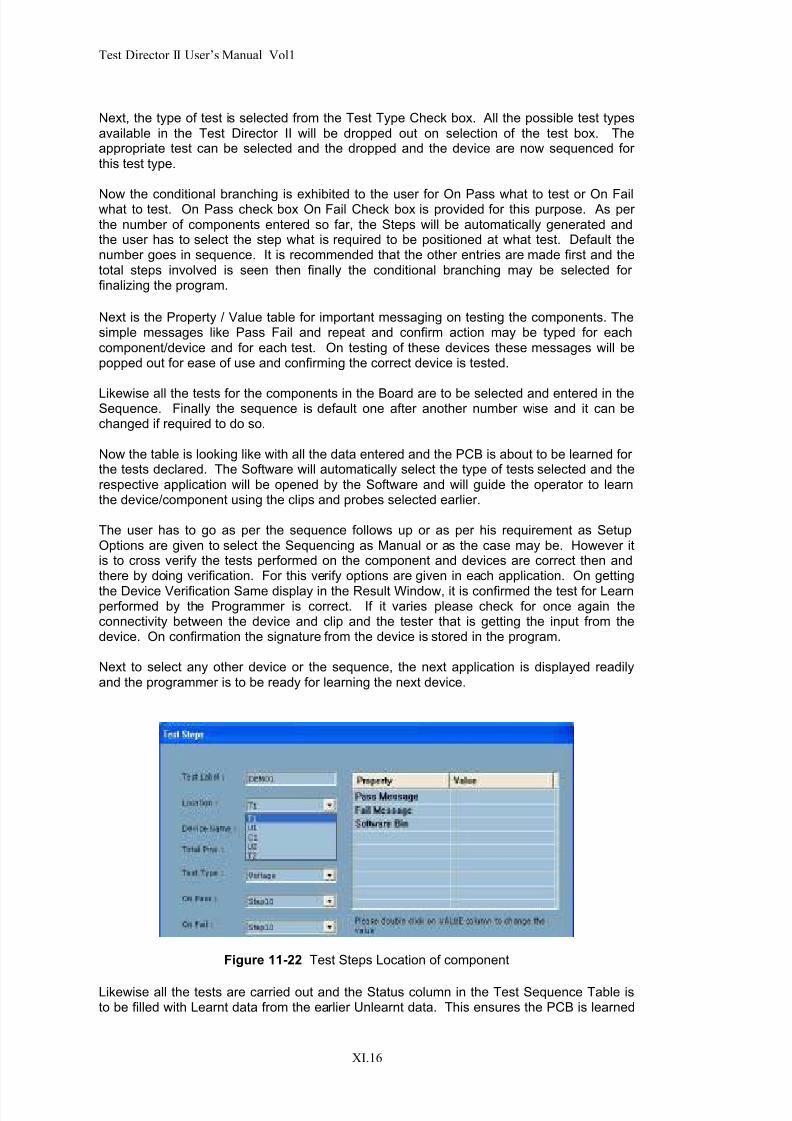
8/3/2019 V200UserManual
http://slidepdf.com/reader/full/v200usermanual 154/171
Test Director II User’s Manual Vol1
XI.16
Next, the type of test is selected from the Test Type Check box. All the possible test typesavailable in the Test Director II will be dropped out on selection of the test box. Theappropriate test can be selected and the dropped and the device are now sequenced for this test type.
Now the conditional branching is exhibited to the user for On Pass what to test or On Failwhat to test. On Pass check box On Fail Check box is provided for this purpose. As per the number of components entered so far, the Steps will be automatically generated andthe user has to select the step what is required to be positioned at what test. Default thenumber goes in sequence. It is recommended that the other entries are made first and thetotal steps involved is seen then finally the conditional branching may be selected for finalizing the program.
Next is the Property / Value table for important messaging on testing the components. Thesimple messages like Pass Fail and repeat and confirm action may be typed for eachcomponent/device and for each test. On testing of these devices these messages will bepopped out for ease of use and confirming the correct device is tested.
Likewise all the tests for the components in the Board are to be selected and entered in theSequence. Finally the sequence is default one after another number wise and it can bechanged if required to do so.
Now the table is looking like with all the data entered and the PCB is about to be learned for the tests declared. The Software will automatically select the type of tests selected and therespective application will be opened by the Software and will guide the operator to learnthe device/component using the clips and probes selected earlier.
The user has to go as per the sequence follows up or as per his requirement as SetupOptions are given to select the Sequencing as Manual or as the case may be. However itis to cross verify the tests performed on the component and devices are correct then andthere by doing verification. For this verify options are given in each application. On getting
the Device Verification Same display in the Result Window, it is confirmed the test for Learnperformed by the Programmer is correct. If it varies please check for once again theconnectivity between the device and clip and the tester that is getting the input from thedevice. On confirmation the signature from the device is stored in the program.
Next to select any other device or the sequence, the next application is displayed readilyand the programmer is to be ready for learning the next device.
Figure 11-22 Test Steps Location of component
Likewise all the tests are carried out and the Status column in the Test Sequence Table isto be filled with Learnt data from the earlier Unlearnt data. This ensures the PCB is learned

8/3/2019 V200UserManual
http://slidepdf.com/reader/full/v200usermanual 155/171
Test Sequencer
XI.17
for all the components/devices as per the sequencing. Now the sequencing is ready to runfor years at any time. Once the sequence is completed the user can think about thechange of steps as per the requirement and the corresponding steps can be moved up or down using the Move Up and Move Down Buttons provided.
Figure 11- 23 Test Steps Test type selection
Once it is done for all the components and devices the program can be saved in the PC.Now the program is ready for testing.
Figure 11- 24 Test Steps Sequencing Learning mode
Figure 11- 25 Test Sequencer Learn command Configuration.
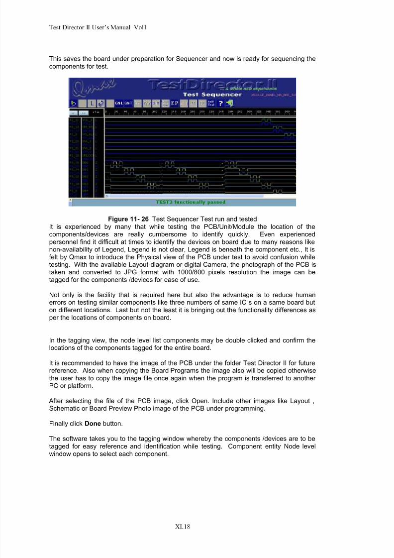
8/3/2019 V200UserManual
http://slidepdf.com/reader/full/v200usermanual 156/171
Test Director II User’s Manual Vol1
XI.18
This saves the board under preparation for Sequencer and now is ready for sequencing thecomponents for test.
Figure 11- 26 Test Sequencer Test run and tested It is experienced by many that while testing the PCB/Unit/Module the location of thecomponents/devices are really cumbersome to identify quickly. Even experiencedpersonnel find it difficult at times to identify the devices on board due to many reasons likenon-availability of Legend, Legend is not clear, Legend is beneath the component etc., It isfelt by Qmax to introduce the Physical view of the PCB under test to avoid confusion whiletesting. With the available Layout diagram or digital Camera, the photograph of the PCB istaken and converted to JPG format with 1000/800 pixels resolution the image can betagged for the components /devices for ease of use.
Not only is the facility that is required here but also the advantage is to reduce humanerrors on testing similar components like three numbers of same IC s on a same board buton different locations. Last but not the least it is bringing out the functionality differences asper the locations of components on board.
In the tagging view, the node level list components may be double clicked and confirm thelocations of the components tagged for the entire board.
It is recommended to have the image of the PCB under the folder Test Director II for futurereference. Also when copying the Board Programs the image also will be copied otherwisethe user has to copy the image file once again when the program is transferred to another PC or platform.
After selecting the file of the PCB image, click Open. Include other images like Layout ,Schematic or Board Preview Photo image of the PCB under programming.
Finally click Done button.
The software takes you to the tagging window whereby the components /devices are to betagged for easy reference and identification while testing. Component entity Node levelwindow opens to select each component.

8/3/2019 V200UserManual
http://slidepdf.com/reader/full/v200usermanual 157/171
Test Sequencer
XI.19
Figure 11- 27 Components in the PCB tagged
For tagging follow the steps for each device:
Keep the cursor onto the component, which is to be tagged.
Drag the cursor so as to cover the entire component.
A new window Entity Name will be popped up.
Select the component, which is under tagging now.
All the components, which are entered in the Devices List, will be dropped out for selection.
On selecting the correct component, click OK
This completes the tagging of one component. Likewise all the components or the requiredcomponents are to be tagged. Once all the components are selected further tagging is notpossible since no entity will be left out. The software will not allow further for any tagging.
Under the entity the selected components nodes will be displayed in the Pins column.
Select the appropriate pins required to be tagged in the component tagged already. Thiswill enhance the help of identifying the pins during testing .
Once the tagging is over press save icon.

8/3/2019 V200UserManual
http://slidepdf.com/reader/full/v200usermanual 158/171
Test Director II User’s Manual Vol1
XI.20
Figure 11- 28 Entity Name Sub-window
Figure 11- 29 Results of Tagging the components
The components entered so far are the ones to be sequenced for various tests to beperformed.

8/3/2019 V200UserManual
http://slidepdf.com/reader/full/v200usermanual 159/171
Test Sequencer
XI.21
Figure 11- 30 component node tagged view
Select Close icon to proceed further.
Thus Sequence of the tests to be performed in the PCB under test is ready now for learning.
One by one learn the results of each tests and the database is automatically stored and thestatus will be seemed as learnt from Unlearnt. The key point to be remembered is that thelearnt responses only will be compared in Testing the PCB and hence the learning is to beproper.
Test
On closing the learn mode the software will take the programmer to the front screen toselect Test mode for testing the PCB under programming.
Now it is to be understood that the data cannot be altered. Only the tests will run as per thesequence ordered and Pass Fail results will be displayed for each test.
It is customary to have one or two tests for each device/component and confirm that theyare passing before finalizing the program.
When all the tests in the Sequence in the Board Program are completed and the result isPass for the entire Board the PCB is assumed to be OK.
In the Result analysis, Pie chart is provided for declaring the status of the Board under testinstantaneously. Pie chart will get updated after the test is carried out and as per the result.Generally for Pass, Fail and Untested conditions the Pie chart is made. This gives theoverall status of Board as per the component list and how many devices or components aretested and found Pass/Fail.

8/3/2019 V200UserManual
http://slidepdf.com/reader/full/v200usermanual 160/171
Test Director II User’s Manual Vol1
XI.22
Figure 11- 31 Resistance Measurement
Figure 11- 32 Voltage Measurements

8/3/2019 V200UserManual
http://slidepdf.com/reader/full/v200usermanual 161/171
Test Sequencer
XI.23
Figure 11- 33 Test Sequencer all tests run and results of Pie chart
XI.7 Special Options Test Types:
User Prompt:
This option is used to caution while testing the Board under test for any importantrequirements. This is selected before or after any tests and the corresponding messages
are to be entered so that while the sequence is running the messages will be popped out inright time. The positioning of these prompts is left to the choice of the user whileprogramming.
The messages can be entered in the Value column and the same will be prompted to theuser while the appropriate test begins and ends.
A sample screen for the same is shown below.
Figure 11- 34 User Prompt Window

8/3/2019 V200UserManual
http://slidepdf.com/reader/full/v200usermanual 162/171
Test Director II User’s Manual Vol1
XI.24
Figure 11- 35 User Prompt Message display WindowDelay
Delay in switching on the BUT Power Supply can be programmed before execution of anytest. This is programmable in mSecs. This enables the Power Supply delay in switchingfor testing
Figure 11- 36 Time Delay in test Steps window
It is designed to facilitate the testing of PCB can be made selective by choosing all thetests, Untested Tests or Failed tests only using the check boxes provided. This window canbe selected from the Run Button drop down list. With this the PCB testing can be proceedto carryout the selected tests. This is useful while testing the PCB with the same serialnumber and restarting the tests with break in operation. Previous passes tests can be
bypassed and untested , Failed tests may be redone.
Figure 11 - 37 Test Sequencer Tests run command config selection window

8/3/2019 V200UserManual
http://slidepdf.com/reader/full/v200usermanual 163/171
Test Sequencer
XI.25
Close Close will close the test or learn mode of the sequencer and will take you to the front screento select the project for further test or edit.
Exit Exit will close the Test Sequencer application module. Before quitting the application it is tobe ensured that the all the test results are to be stored otherwise the data will be lost.
Summary
This chapter completely explained the usage of Test Sequencer package to edit and usewhile repairing PCB/Units.

8/3/2019 V200UserManual
http://slidepdf.com/reader/full/v200usermanual 164/171
Test Director II User’s Manual Vol1
XI.26

8/3/2019 V200UserManual
http://slidepdf.com/reader/full/v200usermanual 165/171
Chapter XII Board Test Station

8/3/2019 V200UserManual
http://slidepdf.com/reader/full/v200usermanual 166/171
Test Director II User’s Manual Vol1
XII.2
Introduction
XII.1 Board Test Station
Board Test Station is used for testing the boards when once the program is made in Test
Sequencer.
Board level testing using combination of ICFT, QSM-VI, Measurements, Card edge test,Boundary Scan Test etc., can be done in one test program through this Station.
The main purpose of test Station is to guide for effective sequencing of Operations to beperformed in the PCB/module to repair and rectify the fault at ease of use.
Board Test Station is used to test the following tests:
Open/Short Testing
Device In-circuit /Out-circuit testing
In-Circuit measurements for Inductance, Capacitance, Resistance, Voltage &Frequency.
Functional Testing of PCB/Module through Card Edge connectors.
Boundary Scan Testing of Boundary Scan compliant devices on Board.
User Prompting while repairing the Boards.
External Inputs and In port and out port facilities for easy transferability.
Delay in programming of execution for testing specific modules. Etc.,
One time sequencing of tests to be performed for Lifetime running on similar Boards for effective repair and maintenance.
Once the test is over the failure report of the PCB tested for further analysis.
XII.2 How to: Starting the Board Test Station
Opening the board test station Program
There are two ways you can open the Board Test Station programs in windowsenvironment. You can select the Board Test Station program from your Programs menu.Or, you can double click the Board Test Station shortcut icon in your desktop.
To open the Board Test Station
1. To start the Board Test Station program, click on the Start button, and point toPrograms.
2. Point to the folder named Qmax and then click on the Board Test Station icon in theTest Director II sub-folder.
8/3/2019 V200UserManual
http://slidepdf.com/reader/full/v200usermanual 167/171
Board Test Station
XII.3
Figure 12-1 Starting Board Test Station
3. Created Shortcut Icon for Board Test Station to be placed on Desktop
On clicking the icon the front screen of the Board Test Station will open up.
Figure 12-2. Board Test Window

8/3/2019 V200UserManual
http://slidepdf.com/reader/full/v200usermanual 168/171
Test Director II User’s Manual Vol1
XII.4
If programs are ready for testing available click Open.
On clicking Open button, the List of programs menu will open.
The List of Programs window is illustrated below:
Figure 12-3 List Of Programs Window
Select the board under the selected Project, which is used to test the PCB under test.
Instantaneously, Board Serial Number window will open.
Enter the Serial number of the PCB under test.
If the number entered is correct, click OK
Figure 12-4. Board Serial Number Window
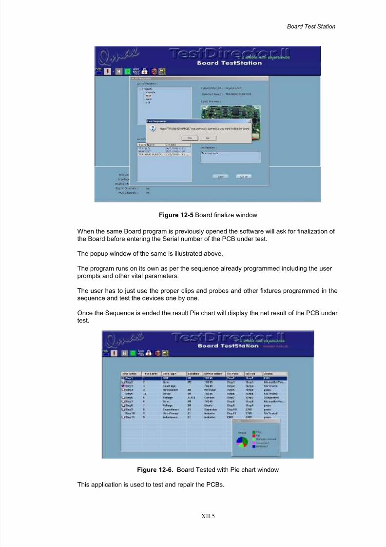
8/3/2019 V200UserManual
http://slidepdf.com/reader/full/v200usermanual 169/171
Board Test Station
XII.5
Figure 12-5 Board finalize window
When the same Board program is previously opened the software will ask for finalization of the Board before entering the Serial number of the PCB under test.
The popup window of the same is illustrated above.
The program runs on its own as per the sequence already programmed including the user prompts and other vital parameters.
The user has to just use the proper clips and probes and other fixtures programmed in thesequence and test the devices one by one.
Once the Sequence is ended the result Pie chart will display the net result of the PCB under test.
Figure 12-6. Board Tested with Pie chart window
This application is used to test and repair the PCBs.

8/3/2019 V200UserManual
http://slidepdf.com/reader/full/v200usermanual 170/171
Test Director II User’s Manual Vol1
XII.6
More than once if the serial number of the PCB entered is same the software will ask for tocontinue with the previous instance or a fresh one to begin with. Enter Yes or NOaccordingly which will refresh the database of the results.
The result report may be printed and be used for further analysis.
While testing if any component or test fails the failure report pops up. User can select therespective status for maintaining and proceed with other tests. Once the board is testedfully these components or tests can be repeated and finalize the board status.
Figure 12-7. Results Window Pie Chart
The result will get updated automatically. Pie chart will bring the results in various colors asindicated
Board History can be seen by results message or in histogram component wise. Theresults can be seen on screen with the user comments for future use.
Previous comments with the status are displayed for easy reference. Histogram for thisserial number of the PCB under test can be seen on screen and the analysis can be madequickly. Thus the Board test station is made useful for testing and analyzing the results of the tested PCB for analysis and making decisions for improvement.
Figure 12-8. Board History window

8/3/2019 V200UserManual
http://slidepdf.com/reader/full/v200usermanual 171/171
Board Test Station
Figure 12-9. Board Failure Report- Histogram component wise
Summary
This chapter explains the usage of Board Test Station package to test the boards by simplemeans.


