Embed Size (px)
Citation preview
University of Central Florida University of Central Florida
STARS STARS
Electronic Theses and Dissertations, 2020-
2021
UV-Ozone Oxide Treatments for High-Efficiency Silicon UV-Ozone Oxide Treatments for High-Efficiency Silicon
Photovoltaic Devices Photovoltaic Devices
Munan Gao University of Central Florida
Part of the Semiconductor and Optical Materials Commons
Find similar works at: https://stars.library.ucf.edu/etd2020
University of Central Florida Libraries http://library.ucf.edu
This Doctoral Dissertation (Open Access) is brought to you for free and open access by STARS. It has been accepted
for inclusion in Electronic Theses and Dissertations, 2020- by an authorized administrator of STARS. For more
information, please contact [email protected].
STARS Citation STARS Citation Gao, Munan, "UV-Ozone Oxide Treatments for High-Efficiency Silicon Photovoltaic Devices" (2021). Electronic Theses and Dissertations, 2020-. 504. https://stars.library.ucf.edu/etd2020/504
UV-OZONE OXIDE TREATMENTS FOR HIGH-EFFICIENCY SILICON
PHOTOVOLTAIC DEVICES
by
MUNAN GAO
B.S. Xidian University, 2010
M.S. University of Chinese Academy of Science, 2015
M.S. University of Central Florida, 2018
A dissertation submitted in partial fulfillment of the requirements
for the degree of Doctor of Philosophy
in CREOL, The College of Optics and Photonics
at the University of Central Florida
Orlando, Florida
Spring Term
2021
Major Professor: Winston V. Schoenfeld
ii
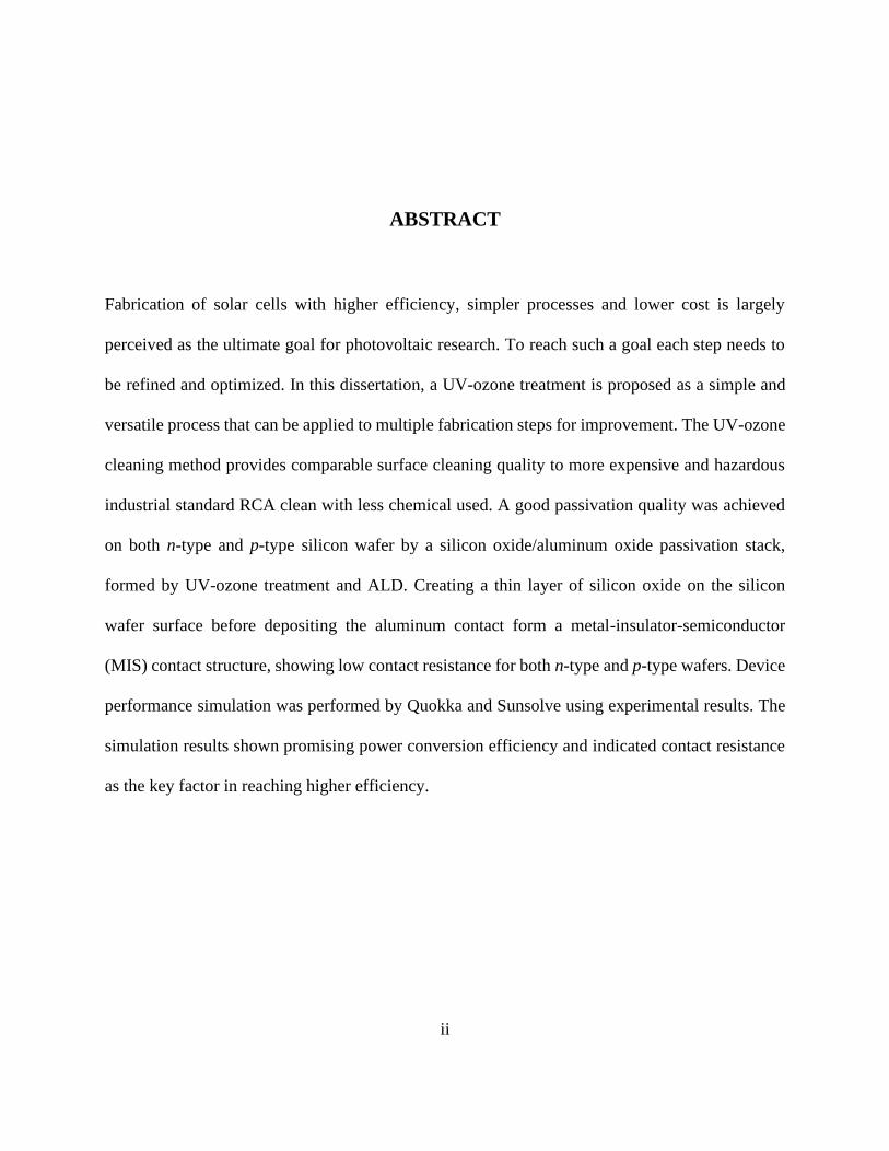
ABSTRACT
Fabrication of solar cells with higher efficiency, simpler processes and lower cost is largely
perceived as the ultimate goal for photovoltaic research. To reach such a goal each step needs to
be refined and optimized. In this dissertation, a UV-ozone treatment is proposed as a simple and
versatile process that can be applied to multiple fabrication steps for improvement. The UV-ozone
cleaning method provides comparable surface cleaning quality to more expensive and hazardous
industrial standard RCA clean with less chemical used. A good passivation quality was achieved
on both n-type and p-type silicon wafer by a silicon oxide/aluminum oxide passivation stack,
formed by UV-ozone treatment and ALD. Creating a thin layer of silicon oxide on the silicon
wafer surface before depositing the aluminum contact form a metal-insulator-semiconductor
(MIS) contact structure, showing low contact resistance for both n-type and p-type wafers. Device
performance simulation was performed by Quokka and Sunsolve using experimental results. The
simulation results shown promising power conversion efficiency and indicated contact resistance
as the key factor in reaching higher efficiency.
iii
ACKNOWLEDGMENTS
Looking back on my 6 years Ph.D. time in CREOL, it is truly a long and amazing trip. One can
achieve nothing without helps and supports from others, and I want to express my sincere thanks
to all of them.
First and foremost, I want to thank my parents. My father Gao Chao and my mother Dong Nili.
They are both experienced engineers, my interest and curiosity of science come from them. It’s
their dedication and support that makes this trip possible in the beginning. This dissertation is a
fruit of their undoubted trust in their son.
I would like to express my deepest appreciation to my advisors Dr. Ngwe Zin and Professor
Winston Schoenfeld. Dr. Zin teaches me everything about solar cells, we work together for the
experiments, the simulations, and the papers. Dr. Schoenfeld gives me priceless advice for research
and future path, greatly supports me as my committee chair. They are the guiding light of this trip,
lead me to the place I stand now.
I also want to extend my gratitude to my committee member Professor Kyle Renshaw, Professor
Peter Delfyett, and Professor Kris Davis for their constructive advice in my candidacy and
iv
proposal. I want to thank Professor David Hagan and Professor Eric Van Stryland for their guide
and support in my first several years at CREOL.
A lone journey is a sad journey. I very much appreciate the company of my officemate Salimeh
Tofighi, the queen of room 231. We enjoyed numerous discussions together, scientific and non-
scientific. I am also grateful to my other friends in CREOL, including but not limited to: Tang
Jialei, Xu Chi, Ren Jinhan, Zhu Zheyuan, Isa Hatipoglu, Zhang Yuanhang, Zhao Peng, Natalia
Munera, Sepehr Benis, Wu Fan, Li Jinxin. Their friendship makes my Ph.D. life abundant and
relax.
I want to thank my friends back in China, Huang Yao, Yang Zhongming, Zhou Han, Yu Guanqun,
Yin Kaixin, Huang Wenyan, Liu Fangjing Wang Shiyu, and Jia Chenyang. With modern
communication technology, I rarely felt homesick.
At last but not least, I would like to express my thank to all the CREOL staff. Rachel Agerton-
Franzetta and Amy Perry for their great support on paperwork during all my Ph.D. James Ross for
technical help and advice. Nathan Aultman for cleanroom support.
v
TABLE OF CONTENTS
LIST OF FIGURES ..................................................................................................................... viii
LIST OF TABLES ......................................................................................................................... xi
CHAPTER 1: INTRODUCTION ................................................................................................... 1
1.1. Background ...................................................................................................................... 1
1.2. Dissertation Outline.......................................................................................................... 5
CHAPTER 2: METHODS AND MATERIALS ............................................................................ 6
2.1 UV Ozone Treatment ............................................................................................................ 6
2.2 AlOx ALD ............................................................................................................................. 8
2.3 Minority Carrier Lifetime Measurement ............................................................................ 12
2.4 Four-Point Probe Measurement of Sheet Resistance .......................................................... 15
2.5 Metal Contact Deposition and Measurement of Contact Resistance .................................. 19
CHAPTER 3: SURFACE PREPARATION: REASON AND PROCESS .................................. 23
3.1. Saw Damage Etching ......................................................................................................... 23
3.2. Surface Cleaning Methods ................................................................................................. 25
3.2.1. RCA Cleaning ............................................................................................................. 26
3.2.2. Ozone Involved Cleaning ........................................................................................... 27
3.3 Experimental Process .......................................................................................................... 31
vi
3.4 Results and Discussion ....................................................................................................... 34
3.5 Summary ............................................................................................................................. 39
CHAPTER 4: PASSIVATING THE SURFACE ......................................................................... 40
4.1 Materials of The Passivation Layer .................................................................................... 40
4.2 Applying UV-Ozone Treatment for Passivation................................................................. 42
4.3 Experiment Process ............................................................................................................. 43
4.4 Results and Discussion ....................................................................................................... 44
4.5 Summary ............................................................................................................................. 53
CHAPTER 5: CONTACT RESISTANCE AND HOW TO DECREASE IT .............................. 54
5.1 Methods of Reducing Contact Resistance .......................................................................... 54
5.2 Experiment Process ............................................................................................................. 57
5.3 Results and Discussion ....................................................................................................... 60
5.4 Investigation of Contact on AlOx Passivation .................................................................... 63
5.4.1 Experiment setup and methods .................................................................................... 63
5.4.2 Experiment Results and Discussion ............................................................................. 66
5.5 Summary ............................................................................................................................. 69
CHAPTER 6: SIMULATION OF THE CELLS .......................................................................... 70
6.1 Simulation Methods and Setup ........................................................................................... 70

vii
6.2 Optical Simulation Results and Discussion ........................................................................ 72
6.3 Cell Simulation Results of Quokka..................................................................................... 75
6.4 Summary ............................................................................................................................. 82
CHAPTER 7: SUMMARY AND CONCLUSION ...................................................................... 83
LIST OF REFERENCE ................................................................................................................ 84
viii
LIST OF FIGURES
Figure 1: Cross-section of a solar cell.[7] ....................................................................................... 2
Figure 2: Picture of a Jelight 42 UV-ozone generator. ................................................................... 6
Figure 3: Schematic picture of the mercury vapor lamp and reaction process[33]. ....................... 7
Figure 4: photo of ALD Cambridge Nanotech Savannah S100. .................................................... 9
Figure 5: Schematic of ALD process[34]. For our experiment, precursor A is water vapor,
precursor B is TMA and the inert carrier gas is nitrogen. ............................................................ 10
Figure 6: Sinton Instruments WCT-120 wafer-lifetime tool ........................................................ 14
Figure 7: Schematic diagram of a four-point probe. ..................................................................... 15
Figure 8: picture of an Ossila four-point probe system ................................................................ 16
Figure 9: SIMS measurement result of boron(left) and phosphorus(right) doped silicon wafer
sample. .......................................................................................................................................... 18
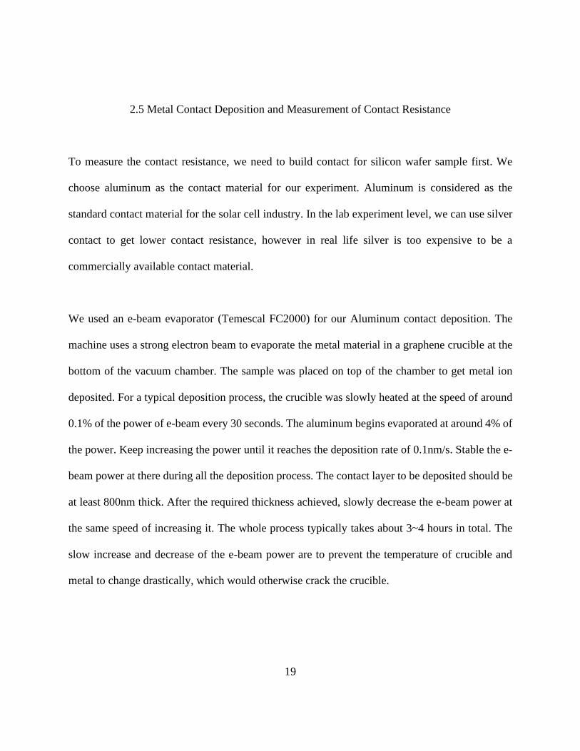
Figure 10: Picture of Temescal FC2000 e-beam evaporator ........................................................ 20
Figure 11: schematic plot of TLM pattern .................................................................................... 21
Figure 12: fitting plot for contact resistance ................................................................................. 22
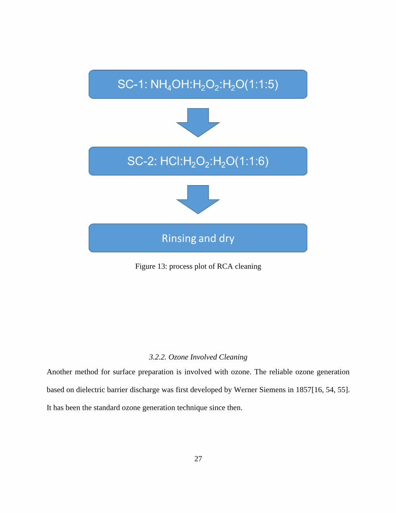
Figure 13: process plot of RCA cleaning ...................................................................................... 27
Figure 14: process plot of DI-O3 cleaning .................................................................................... 28
Figure 15: process plot of UV-Ozone cleaning ............................................................................ 30
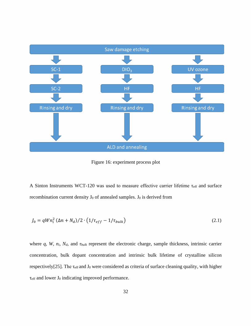
Figure 16: experiment process plot ............................................................................................... 32
Figure 17: Auger-corrected inverse τeff and effective lifetime (inset figure) of samples following
UV ozone clean twice, RCA clean and DI-O3 clean have iVoc of 721,713 and 710 mV respectively.
ix
High τbulk (>10ms) coupled with very low J0(5 fA/cm2) have enabled τeff low to high injection) of
RCA cleaned sample to be significantly higher than the samples cleaned by UV ozone and DI-
O3.[15] ........................................................................................................................................... 34
Figure 18: Auger-corrected inverse τeff of samples applied RCA clean, UV-ozone clean and no
clean. ............................................................................................................................................. 35
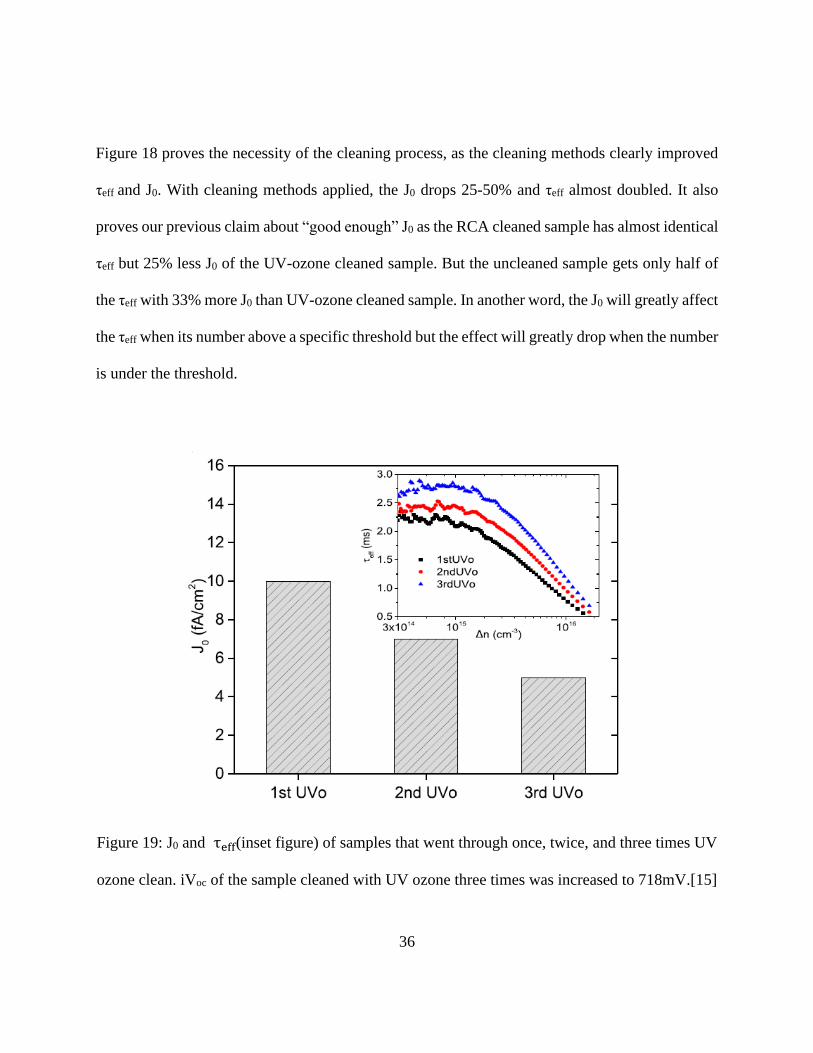
Figure 19: J0 and τeff(inset figure) of samples that went through once, twice, and three times UV
ozone clean. iVoc of the sample cleaned with UV ozone three times was increased to 718mV.[15]
....................................................................................................................................................... 36
Figure 20: Auger-corrected inverse τeff of samples processed for RCA and UV ozone clean with
a varying exposure time of 10 and 5 minutes. Samples with 5 minutes UV ozone clean have iVoc
of 721 and 720mV, respectively.[15] ........................................................................................... 38
Figure 21: Comparison of τeff and J0 (inset figure) between samples passivated by AlOx and
UVo/AlOx stack.[22]..................................................................................................................... 45
Figure 22: HRTEM images of c-Si/AlOx: as-deposited (top left), after annealing (top right); c-
Si/UVo (15 min)/AlOx: as-deposited (bottom left), after annealing (bottom right)..................... 46
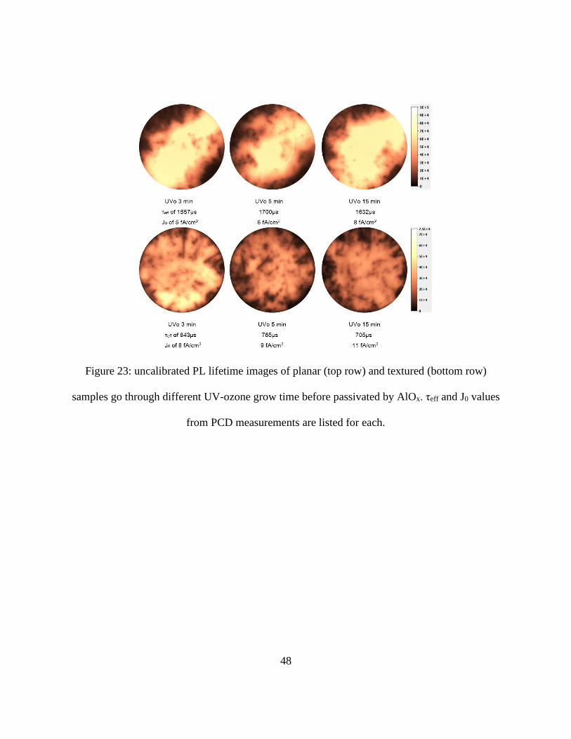
Figure 23: uncalibrated PL lifetime images of planar (top row) and textured (bottom row) samples
go through different UV-ozone grow time before passivated by AlOx. τeff and J0 values from PCD
measurements are listed for each. ................................................................................................. 48
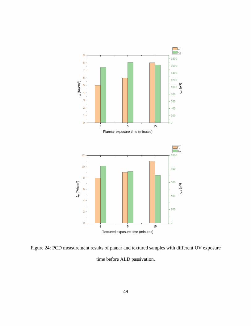
Figure 24: PCD measurement results of planar and textured samples with different UV exposure
time before ALD passivation. ....................................................................................................... 49
x
Figure 25: J0 of AlOx passivated silicon wafers. The different doping concentration of n-type and
p-type samples are shown, respectively. ....................................................................................... 52
Figure 26: schematic pictures of different designs for reducing contact resistance. (a) selective
emitter, (b) MISSM, (c) MIS-IL, (d) MINP ................................................................................. 56
Figure 27: TLM mask design ........................................................................................................ 58
Figure 28: contact resistivity of (a) p-type and (b) n-type samples following different TMAH
etching time to create diffusion situation from light to heavy. ..................................................... 60
Figure 29: structure scheme of the experiment sample ................................................................ 64
Figure 30: I-V curve of the sample measured at different temperature ........................................ 66
Figure 31: the fitting curve of space-limited-charge relation(upper) and thermionic emission
relation(lower)............................................................................................................................... 67
Figure 32: I-V curve of the annealed sample measured at different temperature ......................... 68
Figure 33: equivalent photon current density by different simulation setting .............................. 72
Figure 34: simulation cell geometry generated by Quokka. ......................................................... 75
Figure 35: Contour plot of simulated cell efficiency vs sample parameters variable. (a)the sheet
resistance and J0 were fixed as boron J0=10fA/cm2, sheet resistance 115Ω/□ . Phosphorus
J0=15fA/cm2, sheet resistance 90Ω/□. (b)the contact resistivity and J0 were fixed as boron contact
resistivity 1mΩ.cm2, J0=12fA/cm2. Phosphorus contact resistivity 10mΩ.cm2, J0=25fA/cm2. (c)the
contact resistivity and sheet resistance were fixed as boron contact resistivity 1 mΩ.cm2, sheet
resistance 115Ω/□. Phosphorus contact resistivity 10 mΩ.cm2, sheet resistance 90Ω/□. ......... 80

xi
LIST OF TABLES
Table 1: Basic carrier transport types ........................................................................................... 65
Table 2: Parameters used in the simulation. ................................................................................. 76
Table 3: Efficiency change based on different variable................................................................ 81
1
CHAPTER 1: INTRODUCTION
1.1. Background
Photovoltaic energy relies on the process of converting sunlight directly into electricity by solar
cells. An early observation of the photovoltaic effect and attempt to make use of it can go back to
19 centuries. But even the best effort at that time was less than 1 percent efficient at converting
light to electricity. The first practical silicon solar cell was demonstrated by Bell Laboratories on
April 25, 1954[1]. It had about 6% efficiency. Since then the solar cell growth quickly. In the
1960s due to the space race solar cell was selected as the power supply for satellites, attract a lot
of intention and funds in this area of research. And the oil crisis in the 1970s forced people to look
for alternative energy sources, the solar cell being a strong candidate. The efficiency of solar cells
has increased steadily over time. It reached a milestone of 20% in 1985[2] and now is more than
40%[3]. More and more materials are used to build a solar cell. Aside from the well-known silicon
wafer, there are cadmium telluride (CdTe)[4], gallium arsenide (GaAs)[5], germanium (Ge)[6] and
so on. The industry of solar cell is also growing stable and fast, experienced more than 10% per
year growth rate in decades. In one sentence, solar cell is a strong and active area for both research
and work.
2
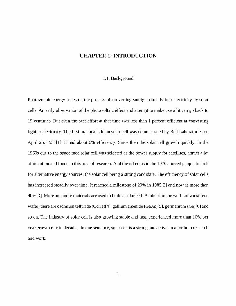
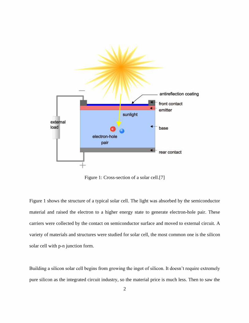
Figure 1: Cross-section of a solar cell.[7]
Figure 1 shows the structure of a typical solar cell. The light was absorbed by the semiconductor
material and raised the electron to a higher energy state to generate electron-hole pair. These
carriers were collected by the contact on semiconductor surface and moved to external circuit. A
variety of materials and structures were studied for solar cell, the most common one is the silicon
solar cell with p-n junction form.
Building a silicon solar cell begins from growing the ingot of silicon. It doesn’t require extremely
pure silicon as the integrated circuit industry, so the material price is much less. Then to saw the
3
ingot into bricks, and further sliced into the wafer. The wafer will be cleaned and textured. The
next step is emitter diffusion to create emitter layer and p-n junction. Edge isolation is needed to
isolate this front emitter from the cell rear. The anti-reflection layer was coated to help absorb
light. Finally, the front and rear contact were deposited.
Making solar cells with higher efficiency, simpler process and lower cost is an endless path of
pursuing. To reach that goal, each step during the fabrication needs to be optimized. Surface
cleaning is a key factor to device performance, only effective cleaning can lead to high-quality
performance. Over the years, various approach of cleaning method has been applied. The well-
known RCA clean is considered as the primary method of wet chemical cleaning in the
microelectronic industry[8]. And a potential replacement named “IMEC-Clean” due to its simpler
process but near-perfect removal of metallic particles was introduced later[9]. On the other hand,
dry cleaning like plasma etch[10] and cryogenic cleaning[11] was considered as a valuable
complement to reach optimized results in certain process sequence. Ozone involved cleaning was
also discussed[12-15] due to its strong oxidizing ability and easy to generate by dielectric barrier
discharge[16].
Surface passivation is another important process for pursuing high conversion efficiency. The
passivation helps to prevent unwanted recombination of photogenerated electron-hole pairs in two
ways[17]. It completes the dangling bonds by a surface dielectric coating or chemical species,
usually referred as the chemical passivation. It also reduces the minority carrier density on the
4
surface to lower recombination rate, referred as electrical passivation. Multiple materials are
studied as passivation layer for silicon solar cells such as silicon oxide[18], silicon nitride[19],
amorphous silicon[20], aluminum oxide[13, 21, 22], titanium oxide[23] and so on.
Contact resistance is also important to power conversion efficiency. the intimate metal-silicon
contact leads to recombination losses due to a high density of states at the metal-silicon
interface[24]. Using high-temperature functional-impurity doping beneath the metal terminal is a
way to drastically lowering the contact resistance. But absorber doping induces its own
fundamental energy losses like Auger recombination, bandgap narrowing and free-carrier
absorption to limit the device performance[25-28]. Metal-insulator-semiconductor (MIS) contact
is another approach to reduce contact recombination losses. A thin film of inserted between the
silicon wafer and the metal terminal, physically separate them to prevent the recombination loss
of direct contact but thin enough to allow current flows. A range of different structures and
materials are discussed[29-32].
5
1.2. Dissertation Outline
This dissertation is organized as follows: CHAPTER 2: Methods and Materials. This chapter
introduces all the equipment and methods were used in this dissertation. CHAPTER 3: Surface
Preparation: Reason and Process. This chapter discusses how the defect of the wafer surface
happens and various methods to remove them. The UV-Ozone method is experimentally proved
to be a candidate with high quality, low cost, and simple process for surface cleaning. CHAPTER
4: Passivating the Surface. This chapter introduces reasons for surface passivation and several
methods to achieve it. The UV-Ozone treatment is proved to be able to improve the passivation
quality. CHAPTER 5: Contact Resistance and How to Decrease it. This chapter explaines methods
to lower the contact resistance. UV-Ozone generated interlayer shown promising low resistance
results. CHAPTER 6: Simulation of the Cells. This chapter shows the simulation results of cells
using experimental parameters from previous chapters. We also discuss how different factors
affect cell simulation results, respectively. CHAPTER 7: Summary and Conclusion summarizes
the concept studied and conclude all the works presented above.
6
CHAPTER 2: METHODS AND MATERIALS
In this chapter, the key pieces of equipment, general experiment process applied, and standard
measurements to define the quality of these processes is presented.
2.1 UV Ozone Treatment
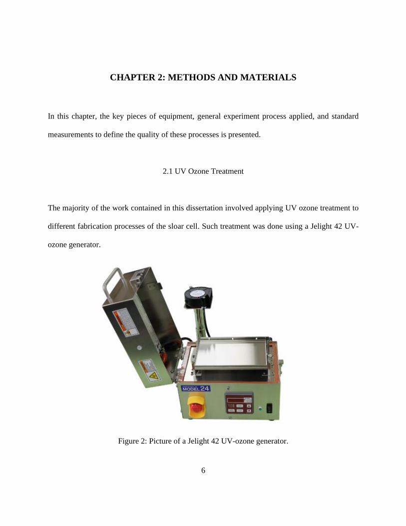
The majority of the work contained in this dissertation involved applying UV ozone treatment to
different fabrication processes of the sloar cell. Such treatment was done using a Jelight 42 UV-
ozone generator.
Figure 2: Picture of a Jelight 42 UV-ozone generator.
7
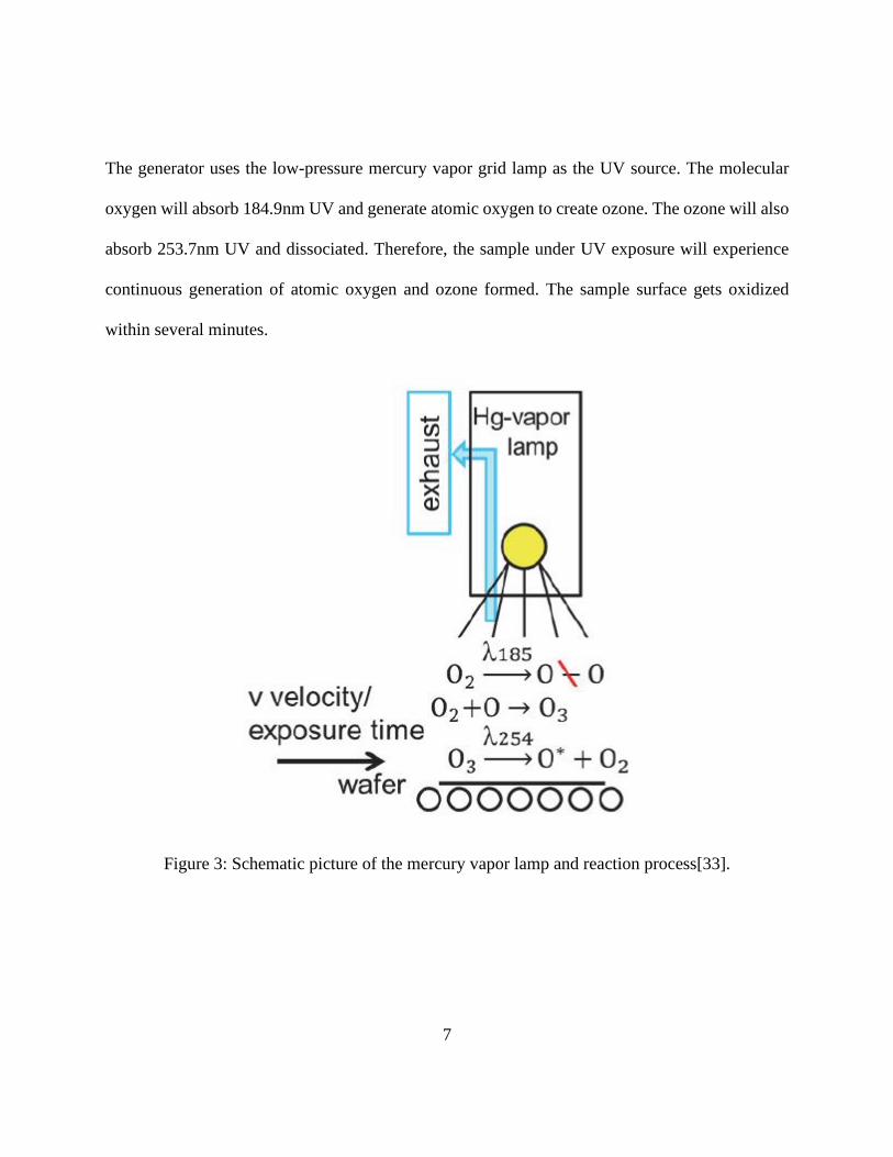
The generator uses the low-pressure mercury vapor grid lamp as the UV source. The molecular
oxygen will absorb 184.9nm UV and generate atomic oxygen to create ozone. The ozone will also
absorb 253.7nm UV and dissociated. Therefore, the sample under UV exposure will experience
continuous generation of atomic oxygen and ozone formed. The sample surface gets oxidized
within several minutes.
Figure 3: Schematic picture of the mercury vapor lamp and reaction process[33].
8
2.2 AlOx ALD
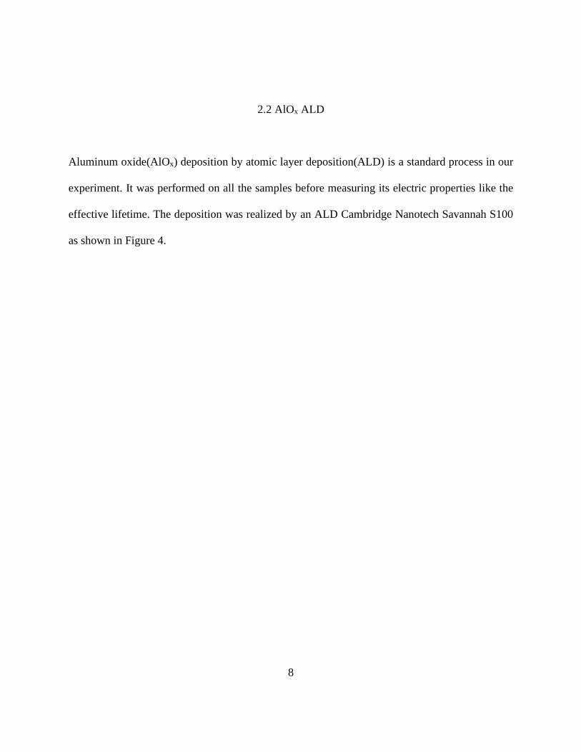
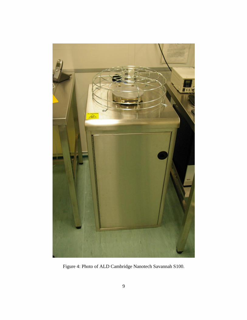
Aluminum oxide(AlOx) deposition by atomic layer deposition(ALD) is a standard process in our
experiment. It was performed on all the samples before measuring its electric properties like the
effective lifetime. The deposition was realized by an ALD Cambridge Nanotech Savannah S100
as shown in Figure 4.
9
Figure 4: Photo of ALD Cambridge Nanotech Savannah S100.
10
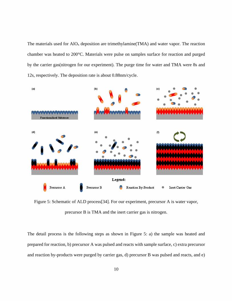
The materials used for AlOx deposition are trimethylamine(TMA) and water vapor. The reaction
chamber was heated to 200°C. Materials were pulse on samples surface for reaction and purged
by the carrier gas(nitrogen for our experiment). The purge time for water and TMA were 8s and
12s, respectively. The deposition rate is about 0.88nm/cycle.
Figure 5: Schematic of ALD process[34]. For our experiment, precursor A is water vapor,
precursor B is TMA and the inert carrier gas is nitrogen.
The detail process is the following steps as shown in Figure 5: a) the sample was heated and
prepared for reaction, b) precursor A was pulsed and reacts with sample surface, c) extra precursor
and reaction by-products were purged by carrier gas, d) precursor B was pulsed and reacts, and e)
11
extra precursor and reaction by-products were purged by carrier gas. Steps b) to e) are considered
as one cycle of deposition. As shown by f), the cycle is repeated until the sample reached the
designed thickness.
12
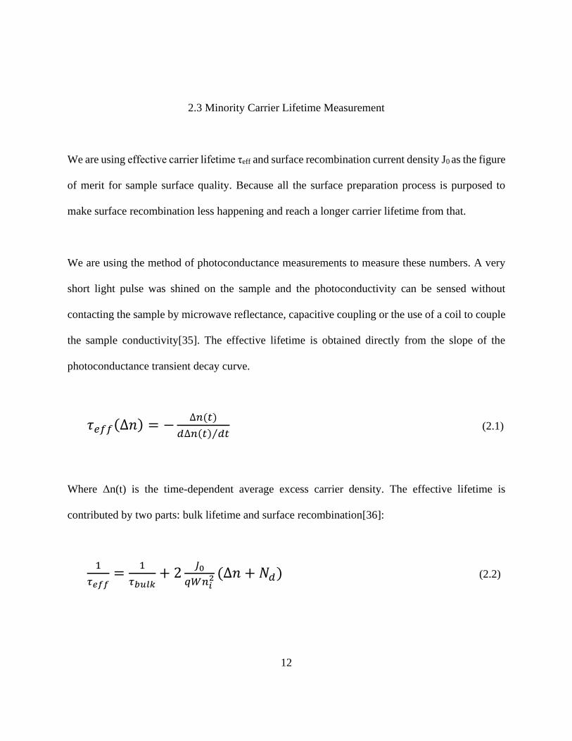
2.3 Minority Carrier Lifetime Measurement
We are using effective carrier lifetime τeff and surface recombination current density J0 as the figure
of merit for sample surface quality. Because all the surface preparation process is purposed to
make surface recombination less happening and reach a longer carrier lifetime from that.
We are using the method of photoconductance measurements to measure these numbers. A very
short light pulse was shined on the sample and the photoconductivity can be sensed without
contacting the sample by microwave reflectance, capacitive coupling or the use of a coil to couple
the sample conductivity[35]. The effective lifetime is obtained directly from the slope of the
photoconductance transient decay curve.
𝜏𝑒𝑓𝑓(∆𝑛) = −∆𝑛(𝑡)
𝑑∆𝑛(𝑡) 𝑑𝑡⁄ (2.1)
Where Δn(t) is the time-dependent average excess carrier density. The effective lifetime is
contributed by two parts: bulk lifetime and surface recombination[36]:
1
𝜏𝑒𝑓𝑓=
1
𝜏𝑏𝑢𝑙𝑘+ 2
𝐽0
𝑞𝑊𝑛𝑖2 (∆𝑛 + 𝑁𝑑) (2.2)
13
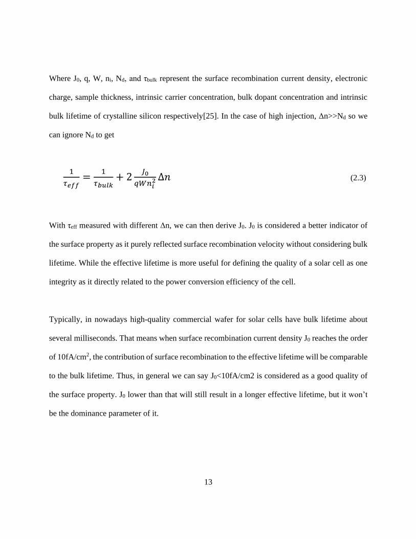
Where J0, q, W, ni, Nd, and τbulk represent the surface recombination current density, electronic
charge, sample thickness, intrinsic carrier concentration, bulk dopant concentration and intrinsic
bulk lifetime of crystalline silicon respectively[25]. In the case of high injection, Δn>>Nd so we
can ignore Nd to get
1
𝜏𝑒𝑓𝑓=
1
𝜏𝑏𝑢𝑙𝑘+ 2
𝐽0
𝑞𝑊𝑛𝑖2 ∆𝑛 (2.3)
With τeff measured with different Δn, we can then derive J0. J0 is considered a better indicator of
the surface property as it purely reflected surface recombination velocity without considering bulk
lifetime. While the effective lifetime is more useful for defining the quality of a solar cell as one
integrity as it directly related to the power conversion efficiency of the cell.
Typically, in nowadays high-quality commercial wafer for solar cells have bulk lifetime about
several milliseconds. That means when surface recombination current density J0 reaches the order
of 10fA/cm2, the contribution of surface recombination to the effective lifetime will be comparable
to the bulk lifetime. Thus, in general we can say J0<10fA/cm2 is considered as a good quality of
the surface property. J0 lower than that will still result in a longer effective lifetime, but it won’t
be the dominance parameter of it.
14
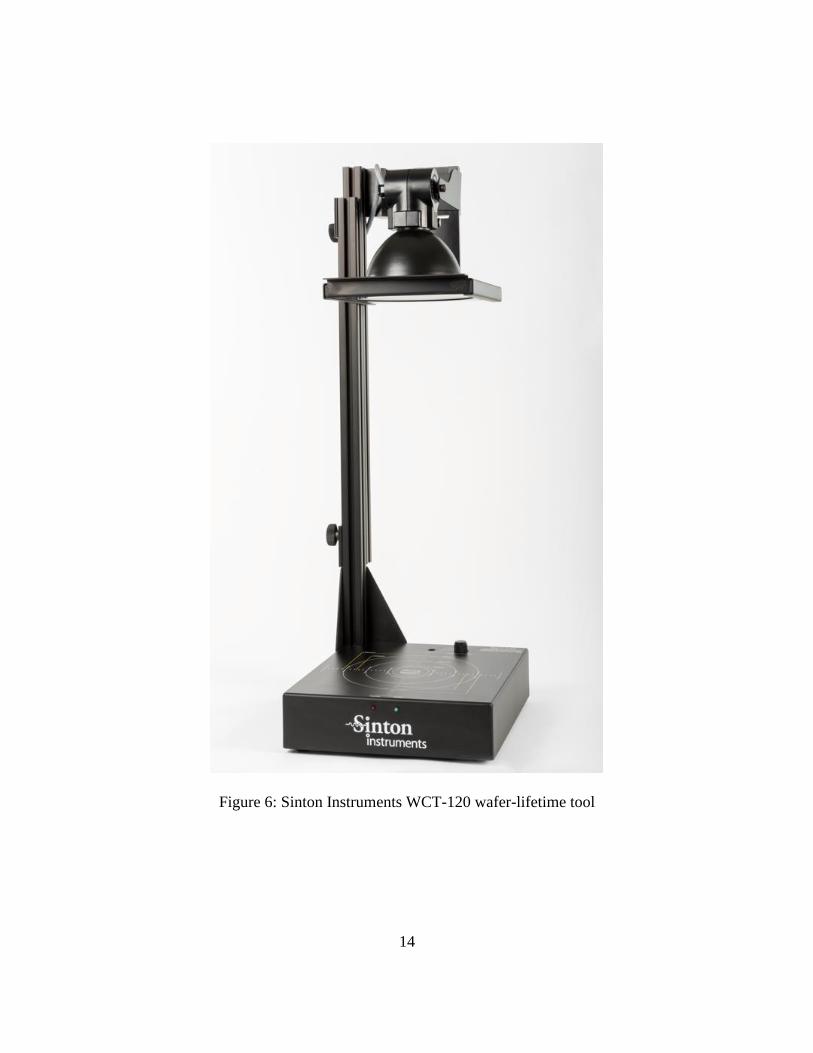
Figure 6: Sinton Instruments WCT-120 wafer-lifetime tool
15
2.4 Four-Point Probe Measurement of Sheet Resistance
We are using the method of four-point probe measurement to measure the sheet resistance of the
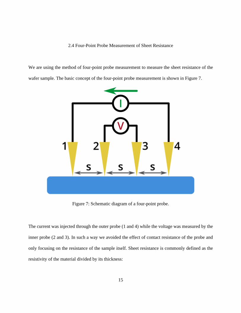
wafer sample. The basic concept of the four-point probe measurement is shown in Figure 7.
Figure 7: Schematic diagram of a four-point probe.
The current was injected through the outer probe (1 and 4) while the voltage was measured by the
inner probe (2 and 3). In such a way we avoided the effect of contact resistance of the probe and
only focusing on the resistance of the sample itself. Sheet resistance is commonly defined as the
resistivity of the material divided by its thickness:
16
𝑅𝑠 =𝜌
𝑡 (2.4)
The unit of it is Ω. However, this number actually represents the resistance between two sides of
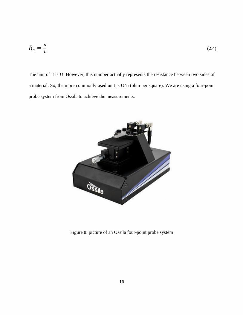
a material. So, the more commonly used unit is Ω/□ (ohm per square). We are using a four-point
probe system from Ossila to achieve the measurements.
Figure 8: picture of an Ossila four-point probe system

17
The sheet resistance we measured is considered as an indicator of the wafer sample’s doping
concentration. As the heavier doped sample will have more carriers, which results in lower sheet
resistance. We also experimentally probed the validity of this indicator.
18
200 400 600 800
1E17
1E18
1E19concentr
ation (
ato
m/c
m3)
Depth (nm)
140W/
115W/
65W/
500 1000
1E17
1E18
1E19
concentr
ation (
ato
ms/c
m3)
Depth (nm)
160W/
120W/
90W/
60W/
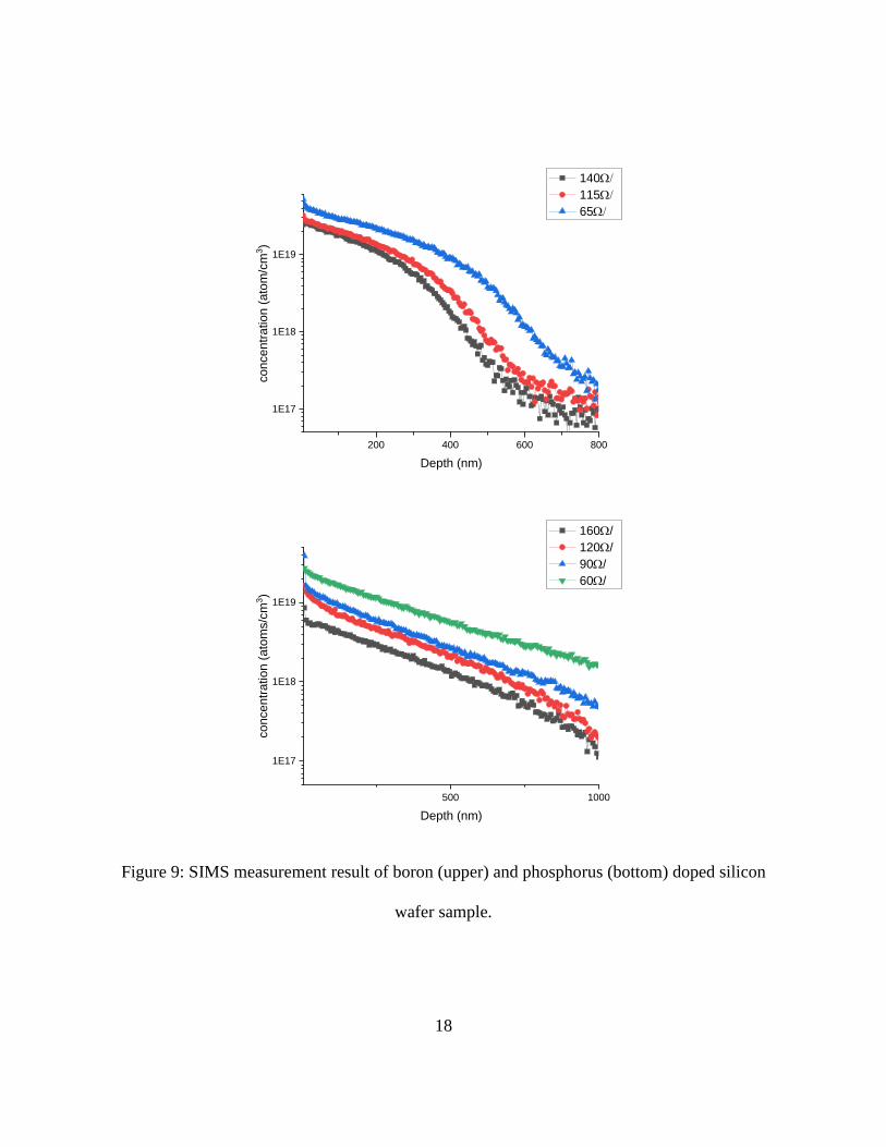
Figure 9: SIMS measurement result of boron (upper) and phosphorus (bottom) doped silicon
wafer sample.
19
2.5 Metal Contact Deposition and Measurement of Contact Resistance
To measure the contact resistance, we need to build contact for silicon wafer sample first. We
choose aluminum as the contact material for our experiment. Aluminum is considered as the
standard contact material for the solar cell industry. In the lab experiment level, we can use silver
contact to get lower contact resistance, however in real life silver is too expensive to be a
commercially available contact material.
We used an e-beam evaporator (Temescal FC2000) for our Aluminum contact deposition. The
machine uses a strong electron beam to evaporate the metal material in a graphene crucible at the
bottom of the vacuum chamber. The sample was placed on top of the chamber to get metal ion
deposited. For a typical deposition process, the crucible was slowly heated at the speed of around
0.1% of the power of e-beam every 30 seconds. The aluminum begins evaporated at around 4% of
the power. Keep increasing the power until it reaches the deposition rate of 0.1nm/s. Stable the e-
beam power at there during all the deposition process. The contact layer to be deposited should be
at least 800nm thick. After the required thickness achieved, slowly decrease the e-beam power at
the same speed of increasing it. The whole process typically takes about 3~4 hours in total. The
slow increase and decrease of the e-beam power are to prevent the temperature of crucible and
metal to change drastically, which would otherwise crack the crucible.
20
Figure 10: Picture of Temescal FC2000 e-beam evaporator
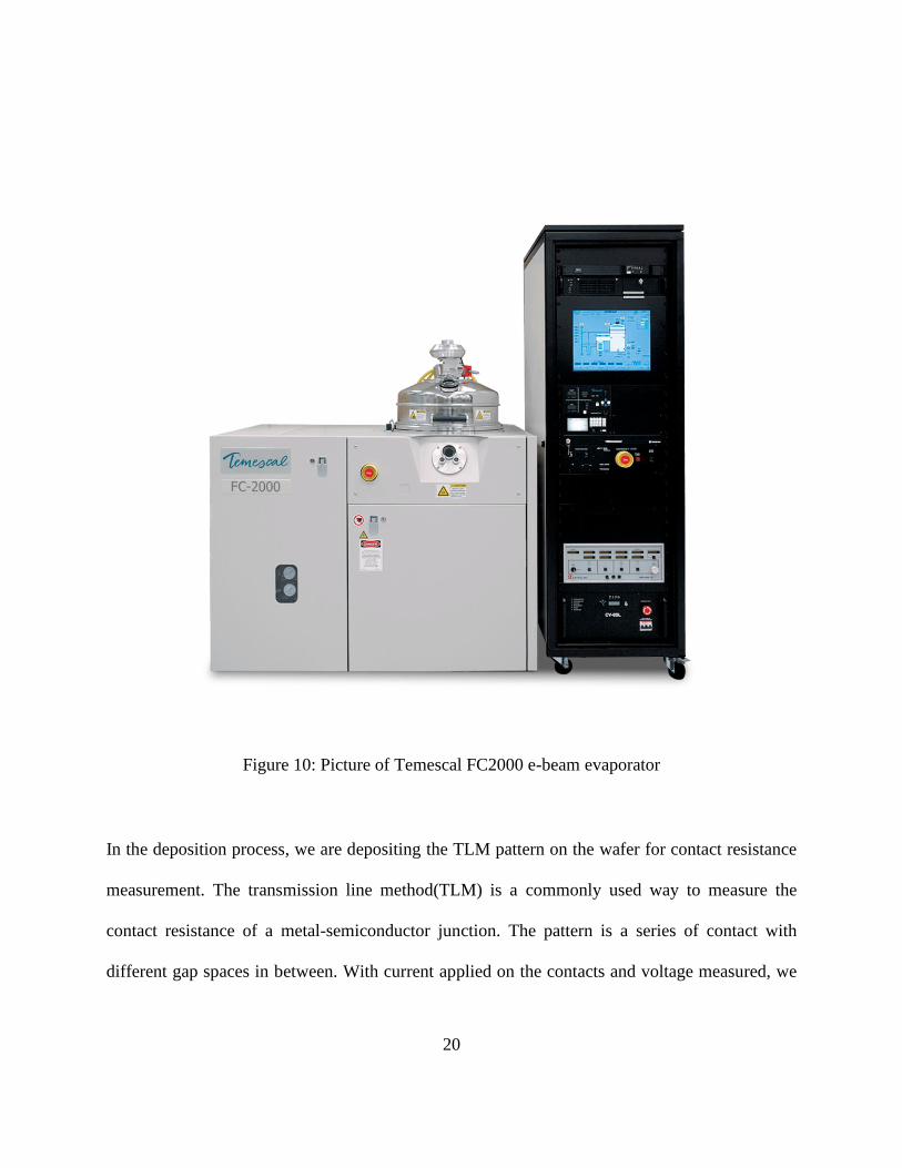
In the deposition process, we are depositing the TLM pattern on the wafer for contact resistance
measurement. The transmission line method(TLM) is a commonly used way to measure the
contact resistance of a metal-semiconductor junction. The pattern is a series of contact with
different gap spaces in between. With current applied on the contacts and voltage measured, we
21
can derive the resistance between the contacts. This resistance is considered to be the combination
of contact resistance and sheet resistance of semiconductor itself:
𝑅𝑇 =𝑅𝑠
𝑊𝐿 + 2𝑅𝑐 (2.5)
Where the RT is the total resistance between the contacts, Rs is the sheet resistance of the
semiconductor, W is the width of the contact pad, L is the gap distance between contacts, Rc is the
contact resistance. By fitting resistance of different contact gap sizes, we can eliminate the effect
of semiconductor resistance and derive the contact resistance.
Figure 11: schematic plot of TLM pattern
22
0.02 0.04 0.06
6
8
10
12
14
Resis
tance (
Ω)
Contact Spacing (cm)
Equation y = a + b*x
Plot Resistance (Ω)
Weight No Weighting
Intercept 2.13847 ± 0.4474
Slope 209.68987 ± 11.2
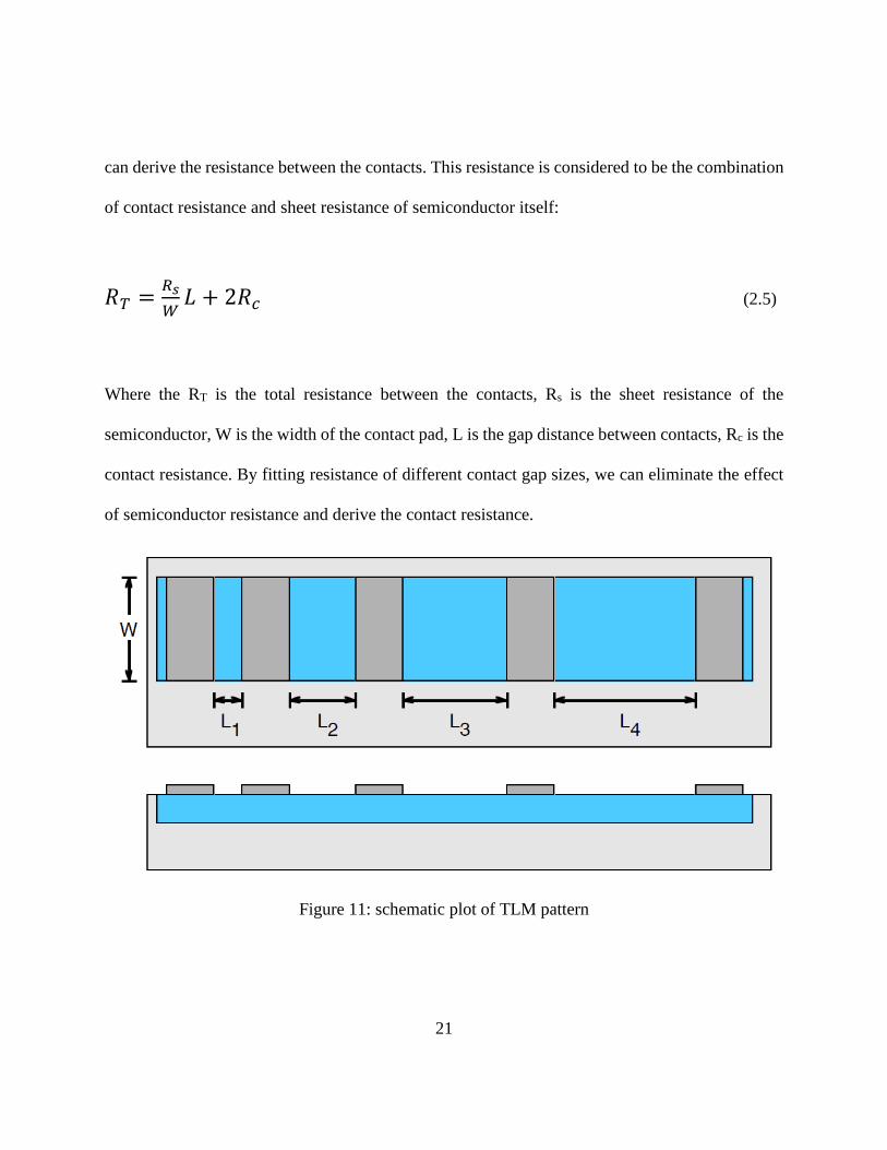
Figure 12: fitting plot for contact resistance
Figure 12 is an example of TLM fitting plot. The fitted intercept is 2Rc so we can derive Rc=1.07Ω.
The slope is Rs/W while W=0.475cm in this case. The fitted sheet resistance Rs=99Ω/□,
comparable to the measured result 90Ω/□.
23
CHAPTER 3: SURFACE PREPARATION: REASON AND PROCESS
Usually, the source material of silicon is in the form of big ingots. We need to saw it into bricks
and then slice to wafer pieces as our initial sample. After all these processes the silicon wafer in
our hand won’t be perfect. There will be saw damage, contaminant, dust and eventually oxide
surface. To acquire good results, we must remove saw damage and clean the sample surface before
fabrication into a PV cell.
3.1. Saw Damage Etching
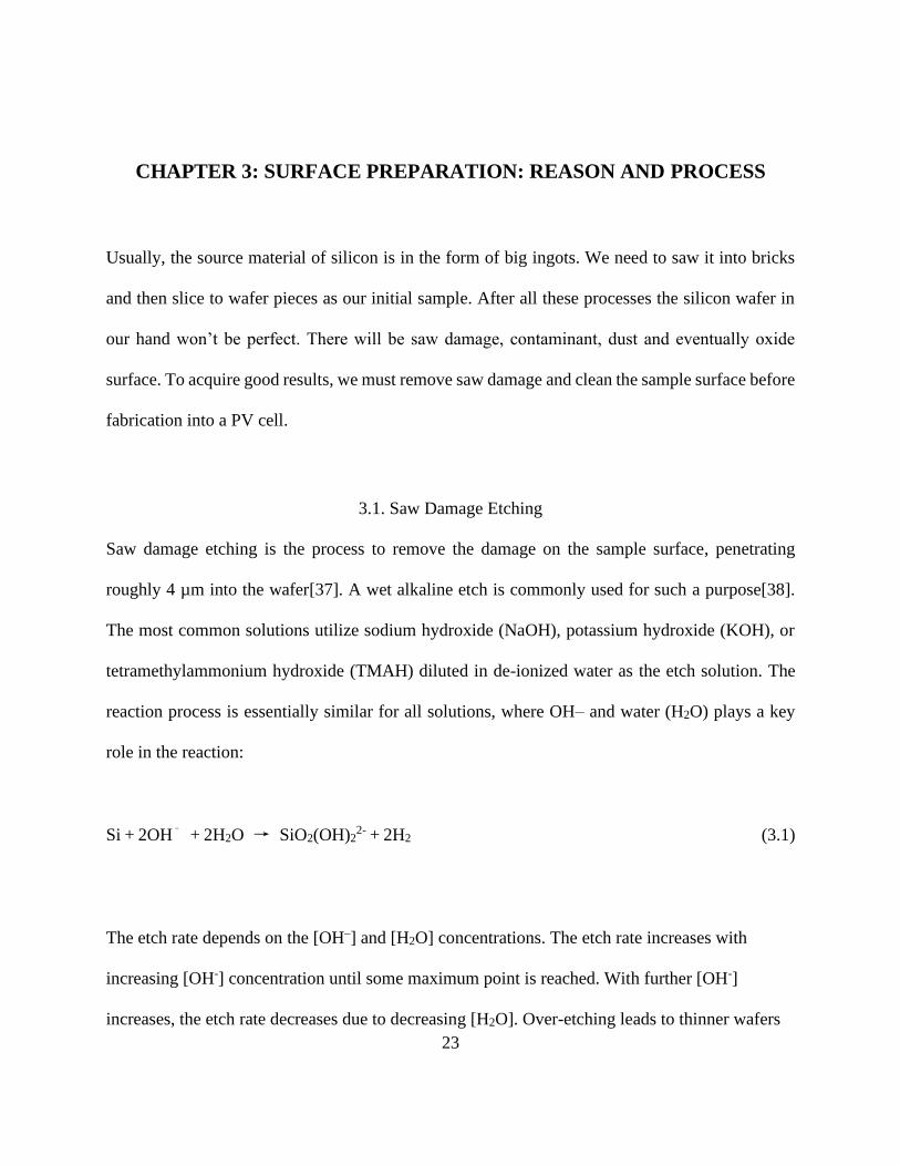
Saw damage etching is the process to remove the damage on the sample surface, penetrating
roughly 4 µm into the wafer[37]. A wet alkaline etch is commonly used for such a purpose[38].
The most common solutions utilize sodium hydroxide (NaOH), potassium hydroxide (KOH), or
tetramethylammonium hydroxide (TMAH) diluted in de-ionized water as the etch solution. The
reaction process is essentially similar for all solutions, where OH– and water (H2O) plays a key
role in the reaction:
Si + 2OH– + 2H2O → SiO2(OH)2
2- + 2H2 (3.1)
The etch rate depends on the [OH–] and [H2O] concentrations. The etch rate increases with
increasing [OH-] concentration until some maximum point is reached. With further [OH-]
increases, the etch rate decreases due to decreasing [H2O]. Over-etching leads to thinner wafers

24
that could lower production yield due to breakage. Under-etching can lead to shunting and
degradation of the minority carrier lifetimes because of residual surface micro-damage.
25
3.2. Surface Cleaning Methods
Surface cleaning in the process intended to remove all the dust, contaminant, particle,
organic/inorganic impurities and native oxide from the wafer surface. It’s a key factor to device
performance, only effective cleaning can lead to high-quality performance. Over the years, various
approach of cleaning method has been applied. The well-known RCA clean is considered as the
primary method of wet chemical cleaning in the microelectronic industry[8]. The process includes
a mixed solution of NH4OH/H2O2/H2O naming SC-1 to remove the organic contaminants, mixed
solution of HCl/H2O2/H2O naming SC-2 to remove inorganic contaminants and ultraclean
deionized water for rinsing. A potential replacement of RCA named “IMEC-Clean” was
introduced later[9]. It has a simpler process that includes a mixture of H2SO4/H2O2 and diluted HF
while reaching near-perfect removal of metallic particles. Ozone is another good candidate
chemical for the cleaning process due to its strong oxidizing ability and easy to generate by
dielectric barrier discharge[16]. The benefits and applications of ozonated deionized water (DI-
O3) for wafer surface preparation was first discussed in detail by Chen[39] and reported by several
groups[40-42]. Bakhshi et al. also represented using DI-O3 for surface preparation before dielectric
layer passivation can achieve outstanding surface passivation quality as the saturation current
density J0 down to 8 fA/cm2(per side)[43]. Aside from wet chemical cleaning, dry cleaning like
plasma etch[10] and cryogenic cleaning[11] was considered as a valuable complement to reach
optimized results in certain process sequence. In general, dry cleaning consumes fewer chemicals
and reduces the possibility of impurity contamination[9, 44-46]. Ozone involved cleaning also has
a dry process version, which is ultraviolet radiation assisted photosensitized oxidation process
26
(UV-ozone process). It was first reported in 1972 by Bolon[47] of able to remove organic residue.
The UV-ozone process was reported to be able to produce a clean surface in less than a minute[48]
and significantly reduce contaminations on chemical cleaned silicon surfaces[49]. The UV-ozone
process also proved to be beneficial to organic photovoltaics. It is reported capable of improving
electron extraction[50], stability in polymer solar cells[51], surface morphology, transmittance and
film quality[52]. It is also used for fluorine-doped tin oxide glass substrate cleaning[53].
3.2.1. RCA Cleaning
Among all these methods, one of the well-known and widely used way is the so-called RCA
cleaning. The basic procedure was developed by Werner Kern in 1965 while working for the Radio
Corporation of America (RCA)[8]. The first step (SC-1) is to prepare a solution with deionized
water, ammonia and hydrogen peroxide as the ratio 5:1:1. Dip wafer in it for 10 minutes at 75 °C
to remove organic residues. Then prepare another solution with deionized water, hydrochloric acid,
and hydrogen peroxide as ratio 6:1:1. Again, dip the wafer in it for 10 minutes at 75 °C to remove
the metallic contaminant. Finally, rinsing with ultrapure deionized water and dry to get a clean
wafer surface.
27
Figure 13: process plot of RCA cleaning
3.2.2. Ozone Involved Cleaning
Another method for surface preparation is involved with ozone. The reliable ozone generation
based on dielectric barrier discharge was first developed by Werner Siemens in 1857[16, 54, 55].
It has been the standard ozone generation technique since then.
28
A process using ozonated deionized water (DI-O3) for wafer surface preparation was discussed in
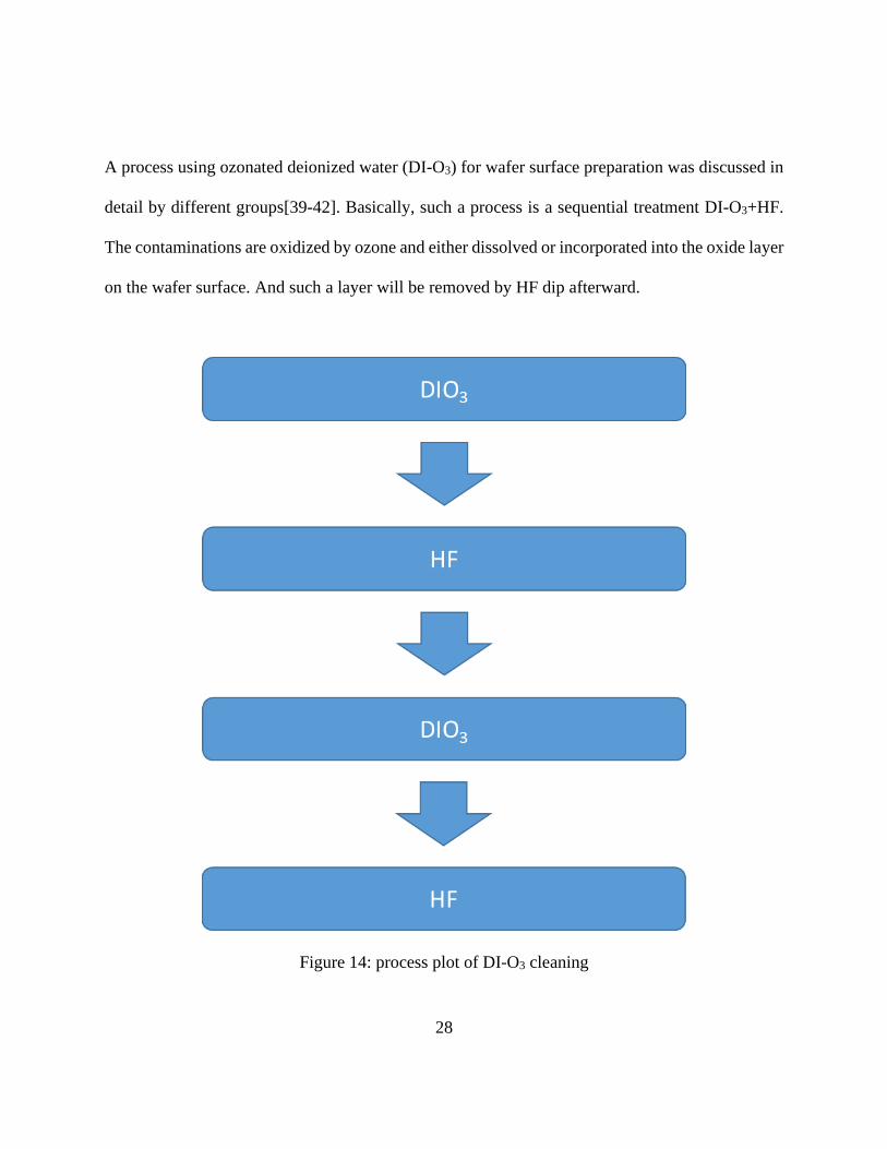
detail by different groups[39-42]. Basically, such a process is a sequential treatment DI-O3+HF.
The contaminations are oxidized by ozone and either dissolved or incorporated into the oxide layer
on the wafer surface. And such a layer will be removed by HF dip afterward.
Figure 14: process plot of DI-O3 cleaning
29
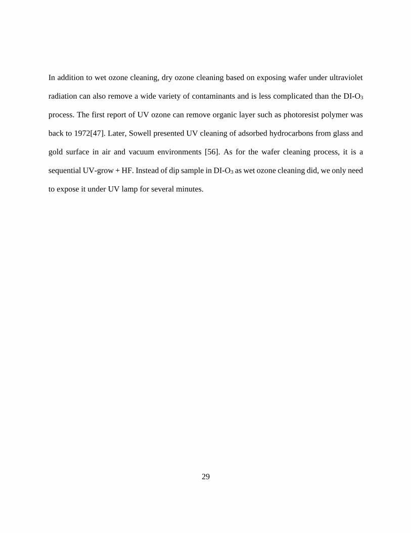
In addition to wet ozone cleaning, dry ozone cleaning based on exposing wafer under ultraviolet
radiation can also remove a wide variety of contaminants and is less complicated than the DI-O3
process. The first report of UV ozone can remove organic layer such as photoresist polymer was
back to 1972[47]. Later, Sowell presented UV cleaning of adsorbed hydrocarbons from glass and
gold surface in air and vacuum environments [56]. As for the wafer cleaning process, it is a
sequential UV-grow + HF. Instead of dip sample in DI-O3 as wet ozone cleaning did, we only need
to expose it under UV lamp for several minutes.
30
Figure 15: process plot of UV-Ozone cleaning
31
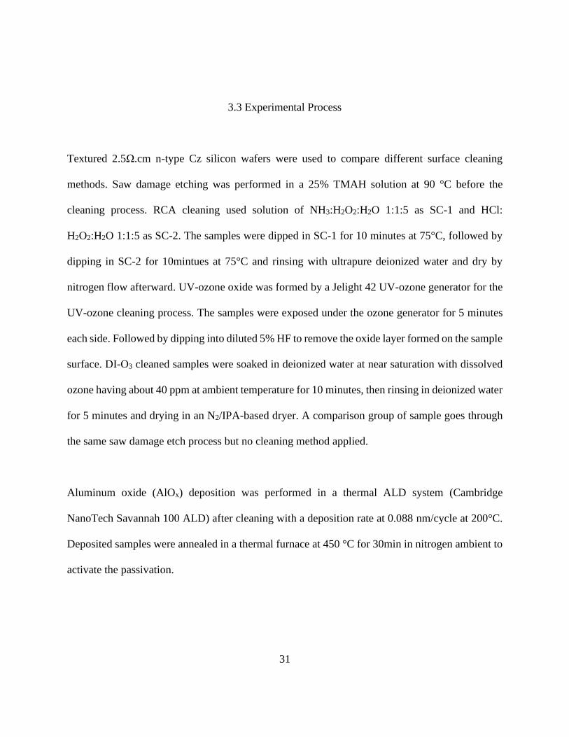
3.3 Experimental Process
Textured 2.5Ω.cm n-type Cz silicon wafers were used to compare different surface cleaning
methods. Saw damage etching was performed in a 25% TMAH solution at 90 °C before the
cleaning process. RCA cleaning used solution of NH3:H2O2:H2O 1:1:5 as SC-1 and HCl:
H2O2:H2O 1:1:5 as SC-2. The samples were dipped in SC-1 for 10 minutes at 75°C, followed by
dipping in SC-2 for 10mintues at 75°C and rinsing with ultrapure deionized water and dry by
nitrogen flow afterward. UV-ozone oxide was formed by a Jelight 42 UV-ozone generator for the
UV-ozone cleaning process. The samples were exposed under the ozone generator for 5 minutes
each side. Followed by dipping into diluted 5% HF to remove the oxide layer formed on the sample
surface. DI-O3 cleaned samples were soaked in deionized water at near saturation with dissolved
ozone having about 40 ppm at ambient temperature for 10 minutes, then rinsing in deionized water
for 5 minutes and drying in an N2/IPA-based dryer. A comparison group of sample goes through
the same saw damage etch process but no cleaning method applied.
Aluminum oxide (AlOx) deposition was performed in a thermal ALD system (Cambridge
NanoTech Savannah 100 ALD) after cleaning with a deposition rate at 0.088 nm/cycle at 200°C.
Deposited samples were annealed in a thermal furnace at 450 °C for 30min in nitrogen ambient to
activate the passivation.
32
Figure 16: experiment process plot
A Sinton Instruments WCT-120 was used to measure effective carrier lifetime τeff and surface
recombination current density J0 of annealed samples. J0 is derived from
𝐽0 = 𝑞𝑊𝑛𝑖2 (∆𝑛 + 𝑁𝑑) 2 ∙ (1/𝜏𝑒𝑓𝑓 − 1/𝜏𝑏𝑢𝑙𝑘)⁄ (2.1)
where q, W, ni, Nd, and τbulk represent the electronic charge, sample thickness, intrinsic carrier
concentration, bulk dopant concentration and intrinsic bulk lifetime of crystalline silicon
respectively[25]. The τeff and J0 were considered as criteria of surface cleaning quality, with higher
τeff and lower J0 indicating improved performance.
33
M-2000 J.A. Woollam spectral ellipsometer was used to measure the thickness of the oxide layer
created by ozone.
34
3.4 Results and Discussion
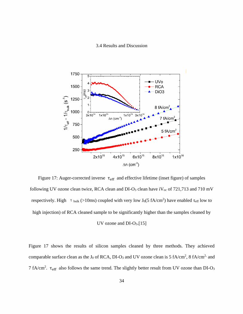
Figure 17: Auger-corrected inverse τeff and effective lifetime (inset figure) of samples
following UV ozone clean twice, RCA clean and DI-O3 clean have iVoc of 721,713 and 710 mV
respectively. High τbulk (>10ms) coupled with very low J0(5 fA/cm2) have enabled τeff low to
high injection) of RCA cleaned sample to be significantly higher than the samples cleaned by
UV ozone and DI-O3.[15]
Figure 17 shows the results of silicon samples cleaned by three methods. They achieved
comparable surface clean as the J0 of RCA, DI-O3 and UV ozone clean is 5 fA/cm2, 8 fA/cm2, and
7 fA/cm2. τeff also follows the same trend. The slightly better result from UV ozone than DI-O3
35
might come from a thicker oxide layer generated by UV. As the mechanism of ozone clean is to
grow oxide of silicon surface and subsequently remove organic and inorganic impurities by etching
such an oxide layer in HF. The thickness of the UV ozone oxide layer is 1.6 nm. While DI-O3
oxide layer thickness is around 1.3 nm. But in general, as we mentioned before, all three methods
can achieve the surface quality of J0 less than 10fA/cm2, which considered a good enough result
for surface cleaning.
3.00E+015 6.00E+015 9.00E+015 1.20E+016 1.50E+016
1000
2000
3000
4000
1/t
eff -
1/t
bu
lk(s
-1)
Excess Carrier Density (cm-3)
RCA 9fA/cm^2
UVo 12fA/cm^2
no clean 16fA/cm^2
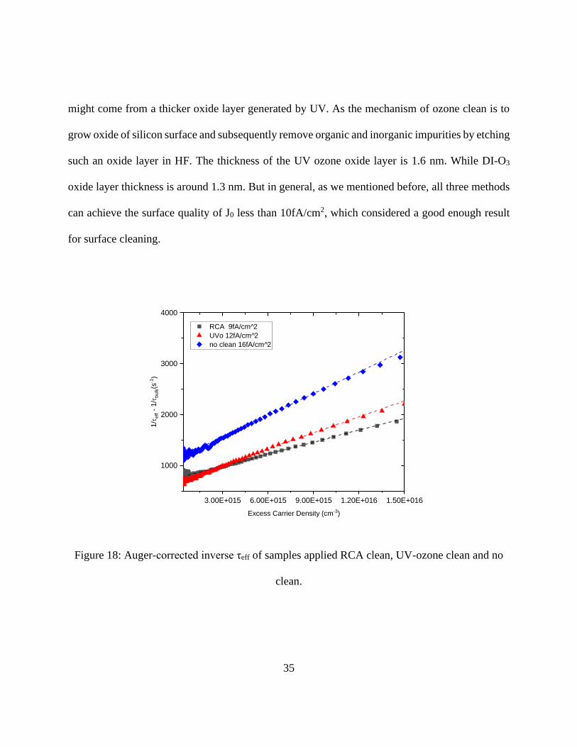
Figure 18: Auger-corrected inverse τeff of samples applied RCA clean, UV-ozone clean and no
clean.
36
Figure 18 proves the necessity of the cleaning process, as the cleaning methods clearly improved
τeff and J0. With cleaning methods applied, the J0 drops 25-50% and τeff almost doubled. It also
proves our previous claim about “good enough” J0 as the RCA cleaned sample has almost identical
τeff but 25% less J0 of the UV-ozone cleaned sample. But the uncleaned sample gets only half of
the τeff with 33% more J0 than UV-ozone cleaned sample. In another word, the J0 will greatly affect
the τeff when its number above a specific threshold but the effect will greatly drop when the number
is under the threshold.
Figure 19: J0 and τeff(inset figure) of samples that went through once, twice, and three times UV
ozone clean. iVoc of the sample cleaned with UV ozone three times was increased to 718mV.[15]
37
Figure 19 proves further sequences of UV ozone treatment can provide an even better clean effect.
1st UVo means the sample only goes through UV exposure and HF dip cycle once. 2nd and 3rd
UVo refer to samples take such cycle twice and three times. As shown in the figure, more cycles
resulted in a longer lifetime and lower J0. Typically, the J0 decreased about 2 fA/cm2 for each extra
cycle of the UVo process. After three times UV ozone process the J0 is already close to RCA
cleaned samples. Again, because the J0 is already “good enough” for even one cycle of UV-ozone
treated sample, the τeff didn’t change much as the cycles increase. But the decrease of J0 shows
UV-ozone cleaning can reach the exact surface quality as RCA cleaning, no matter what the bulk
property is.
Furthermore, since UVo clean is a dry process, it consumes less chemical and the possibilities of
impurities contaminating samples that typically reduce the performance and yield of
semiconductor devices are less than the wet clean process[44-46].
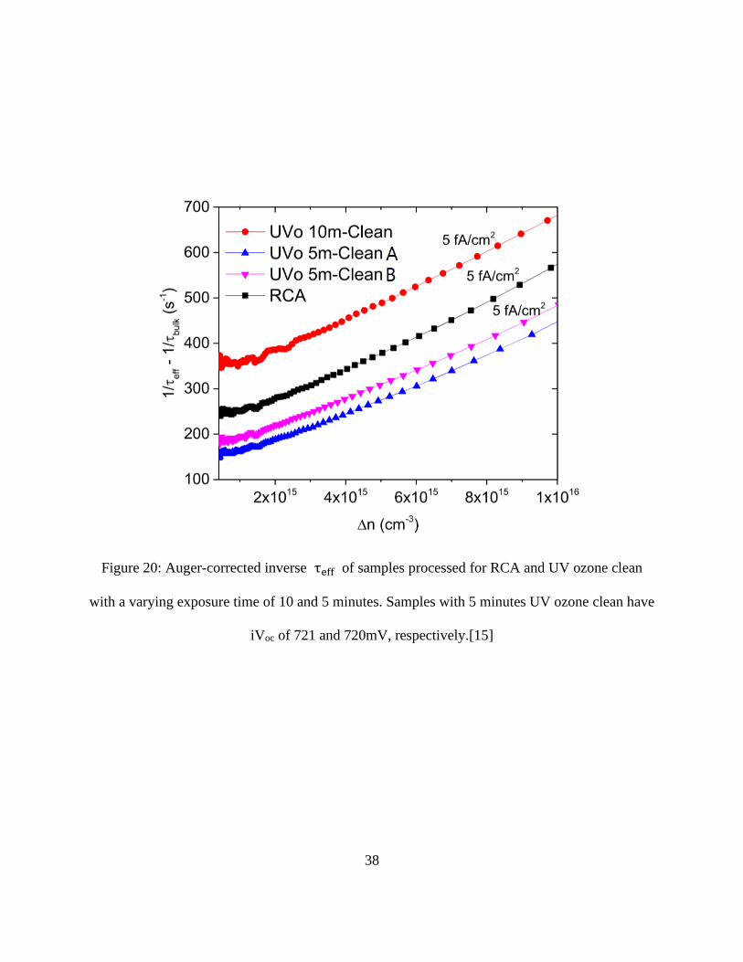
To further simplify the clean process, we reduced UV exposure time to 5 minutes. All the other
processes are the same as the previous experiment. As shown in Figure 20, such reduced time UV
exposure still gives a comparable result. Ellipsometer measurement shows the thickness of the
oxide layer grown by 5 minutes of UV exposure is around 1.4nm. It indicates that such thickness
of UVo is already sufficient to react with organic and inorganic contaminants. The two sample
results of A and B show the good surface quality of the reduced UV exposure time process is
reproducible.
38
Figure 20: Auger-corrected inverse τeff of samples processed for RCA and UV ozone clean
with a varying exposure time of 10 and 5 minutes. Samples with 5 minutes UV ozone clean have
iVoc of 721 and 720mV, respectively.[15]
39
3.5 Summary
We have experimentally proved UV-ozone treatment as a successful method of silicon wafer
surface cleaning. The treatment can be repeated multiple times, each time can prove about 20%
improvement of the cleaning quality. After three times of UV-ozone treatment, the cleaning quality
is close to the industrial standard RCA cleaning result. We also experimentally proved 5 minutes
of exposure time under a UV source is long enough for the UV-ozone cleaning process.
40
CHAPTER 4: PASSIVATING THE SURFACE
Passivation, originally a chemistry process, refers to a material become “passive”, which means
less affected by the environment. While in the semiconductor area, surface passivation especially
refers to the process that creates a thin layer on the semiconductor surface to improve the
performance of the device. Surface passivation is another important process for pursuing high
conversion efficiency. The passivation helps to prevent unwanted recombination of
photogenerated electron-hole pairs in two ways[17]. It completes the dangling bonds by a surface
dielectric coating or chemical species, usually referred as the chemical passivation. It also reduces
the minority carrier density on the surface to lower the recombination rate, referred as electrical
passivation[57].
4.1 Materials of The Passivation Layer
Multiple materials are studied as a passivation layer for silicon solar cells. The thermally grown
silicon dioxide is one of the most common dielectric films in the semiconductor area. Its
passivation quality for silicon solar cell application has been well studied[18, 58]. A so-called
alneal process[59] was introduced to achieve good passivation quality. The thermal SiO2 layer
was deposited with aluminum and then annealed at 400-450°C in a forming gas atmosphere. The
process generates hydrogen and diffused it to the Si-SiO2 interface to improve passivation quality,
the aluminum was stripped by acid later. Silicon nitride (SiNx) is another well-studied passivation
41
material[19, 60-62] and currently the standard film for commercial production of silicon solar
cells[63]. It has several advantages to be such successful. First, the deposition of SiNx is achieved
by the low-temperature method (comparing to SiO2) like PECVD, which is more favorable to mass
production. Second, the deposition and post-deposition anneal release a large amount of hydrogen
to passivates defects on the surface and in bulk. Third, the refractive index of SiNx makes it be an
excellent antireflection coating as well. The combined stack of SiO2/SiNx was also studied and
reported[64, 65]. Introducing aluminum oxide (AlOx) surface layer became one of the main
breakthroughs in surface passivation in the recent two decades. It was first proved to be a capable
passivation layer in the 1980s[66] and attracts research interests until now[21, 22, 67]. The main
advantage of AlOx is its concentration of negative charge[67] rather than the positive charge from
SiO2 and SiNx, which makes it especially suitable for the p-type surface as it won’t induce
inversion layers that lead to shunting loss[57].
42
4.2 Applying UV-Ozone Treatment for Passivation
The benefit of UV-Ozone treatment in organic photovoltaics has been well-studied. It was reported
to be used to treat the ultrathin aluminum and form an alumina interlayer between the active layer
and indium tin oxide (ITO) to improve electron extraction[50]. The UV-Ozone treatment was also
reported to improve the charge collections in dithienogermole–thienopyrrolodione-based polymer
solar cells while treating the zinc oxide–polyvinyl pyrrolidone (ZnO-PVP) nanocomposite film
used as an electron tunneling layer[68]. Aside from electron tunneling layers, UV-Ozone treatment
on the hole collection layer like molybdenum trioxide (MoO3) was reported to improve the surface
morphology, transmittance, and film quality[52]. In addition, UV-Ozone treatment was
demonstrated to change the highest occupied molecular orbital level of Phenyl-C61-butyric acid
methyl ester (PC61BM)[14].
In this chapter, we will discuss in detail how the UV ozone treatment improves the passivation
quality of AlOx.
43
4.3 Experiment Process
Planar 2.5 Ω.cm p-type silicon wafer and textured 2.5 Ω.cm n-type Cz silicon wafer was used in
this experiment. All the samples go through TMAH saw damage etch at 90 °C and UV-ozone
cleaning process before passivation. Samples were exposed under UV light with different time
duration to generate a layer of silicon oxide of different thicknesses. All the samples were
deposited aluminum oxide by thermal ALD and annealed in nitrogen ambient later.
PV2000 Semilab SDI instrument was used to measure effective carrier lifetime τeff and surface
recombination current density J0 of annealed samples. Btimaging LIS-R1 system was used to
obtain the PL image of samples[69]. The images were taken under the quasi-steady-state
photoluminescence (QSS-PL) mode. Cross-sectional TEM specimens were prepared using an FEI
200TEM FIB to obtain the nano-scale interface characterization. HRTEM images were obtained
in the conventional TEM model (FEI Tecnai F30 TEM) at an operating voltage of 300kV.
44
4.4 Results and Discussion
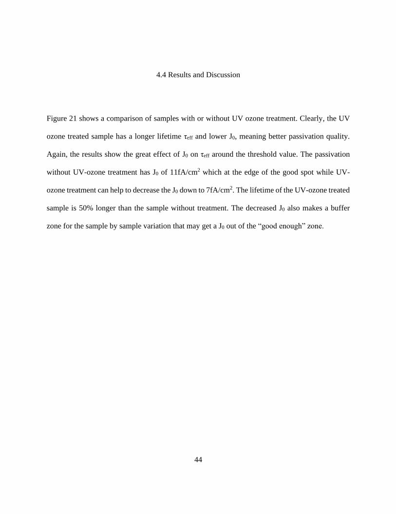
Figure 21 shows a comparison of samples with or without UV ozone treatment. Clearly, the UV
ozone treated sample has a longer lifetime τeff and lower J0, meaning better passivation quality.
Again, the results show the great effect of J0 on τeff around the threshold value. The passivation
without UV-ozone treatment has J0 of 11fA/cm2 which at the edge of the good spot while UV-
ozone treatment can help to decrease the J0 down to 7fA/cm2. The lifetime of the UV-ozone treated
sample is 50% longer than the sample without treatment. The decreased J0 also makes a buffer
zone for the sample by sample variation that may get a J0 out of the “good enough” zone.
45
Figure 21: Comparison of τeff and J0 (inset figure) between samples passivated by AlOx and
UVo/AlOx stack.[22]
46
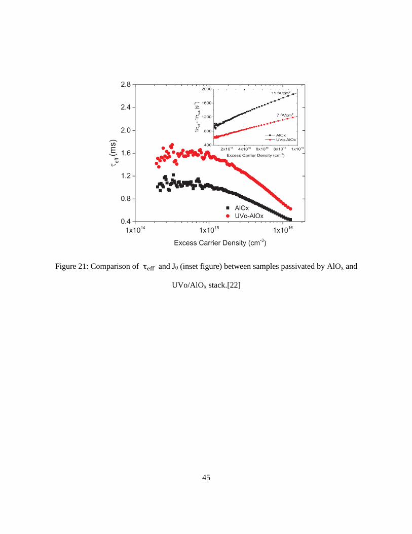
Figure 22: HRTEM images of c-Si/AlOx: as-deposited (top left), after annealing (top right); c-
Si/UVo (15 min)/AlOx: as-deposited (bottom left), after annealing (bottom right).
It can be seen in Figure 22 that a 1-2nm of SiOx interlayer is present at the c-Si/AlOx interface
even in the as-deposited state for samples not subjected to UVo treatment. This indicates that SiOx
was formed during the ALD of AlOx. On the other hand, a 4-5nm of SiOx interlayer is observed at
the c-Si/AlOx interface in the as-deposited state for samples subjected to 15 min UVo treatment.
This indicates that possibly a 3-4nm SiOx layer is formed at Si surface when subjected to UVo
treatment for 15 min which grows further to 4-5nm during subsequent AlOx deposition. In both
cases, HRTEM images reveal no apparent structural change during annealing. In a nutshell,
HRTEM images revealed the presence of a 4-5nm of SiOx layer at the c-Si surface when subjected
47
to 15 min of UVo treatment followed by AlOx deposition. This 4-5nm SiOx layer results in
improved surface passivation as evidenced by the lower J0 value of 7fA/cm2.
48
Figure 23: uncalibrated PL lifetime images of planar (top row) and textured (bottom row)
samples go through different UV-ozone grow time before passivated by AlOx. τeff and J0 values
from PCD measurements are listed for each.
49
3 5 15
0
1
2
3
4
5
6
7
8
9
J0
teff
Plannar exposure time (minutes)
J0 (
fA/c
m2)
0
200
400
600
800
1000
1200
1400
1600
1800
te
ff (
ms)
3 5 15
0
2
4
6
8
10
12
J0
teff
Textured exposure time (minutes)
J0 (
fA/c
m2)
0
200
400
600
800
1000
te
ff (
ms)
Figure 24: PCD measurement results of planar and textured samples with different UV exposure
time before ALD passivation.
50
Similar to the previous chapter, we explored the effect of different UV exposure time on the
passivation stack. Figure 23 shows uncalibrated PL lifetime images of both planar and textured
samples. Figure 24 shows the J0 and τeff of the same samples acquired by PCD measurement. The
planar samples are p-type 2.5Ω-cm silicon wafer and the textured samples are n-type 1.5Ω-cm
silicon wafer, All samples were processed with a UV ozone clean (5 minutes of UV exposure,
followed by HF dip) three times, passivated with a UVo/AlOx stack (different UV exposure time
followed by 10-15 nm AlOx by ALD), and then annealed in N2 at 450 °C for 30 minutes. Such a
process was proved to be the optimized procedure for UV-ozone cleaning and UV-ozone treated
ALD passivation experimentally. Both planar and textured samples show good uniformity. The
τeff and J0 values are extracted by PCD measurement. The τeff of planar samples ranges from 1557
to 1700μs and J0 5 to 8 fA/cm2. The textured samples have a shorter lifetime τeff 705 to 843μs and
higher J0 8 to 11 fA/cm2. The uniformity of textured samples is also worse than the planar sample
as shown in the figure. Slightly poorer passivation on textured samples relative to planar samples
could be attributed to two major reasons. Firstly, since we chose the AlOx as the passivation layer
material, the p-type wafer is supposed to have better passivation quality than the n-type wafer.
Secondly, it may due to an increased surface area of textured pyramids and non-conformal coating
of pyramid peaks by the thin UV ozone passivation layer. But overall, with the reduced UV ozone
oxide layer thickness, samples in this work still get good passivation quality and uniformity.
We further discovered how the passivation quality changes depending on wafer doping
concentration. Both n-type and p-type heavily doped silicon wafers were treated with TMAH etch.
51
Doping concentration was controlled by different etching times. Sheet resistance Rsh were
measured after etching as the indicator of doping concentration, the higher Rsh means the lighter
doped. All the samples go through the 5min UV-ozone grow followed by AlOx passivation. Figure
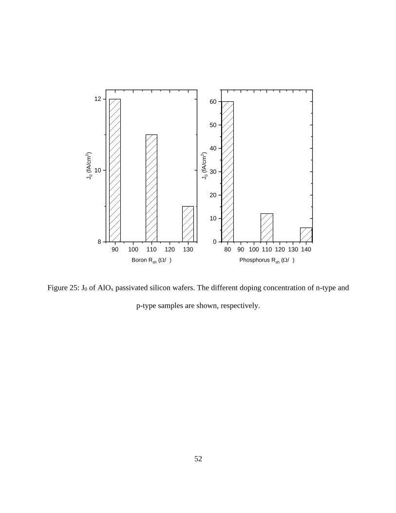
25 shows the J0 from the PCD measurement of passivated samples. Both n-type and p-type results
show better passivation quality with the lighter diffused sample, as the electrical passivation has
more effect on less dopant. The general better result from p-type samples could due to the negative
charge generated during AlOx passivation[57]. It also worth to mention for lightly diffused
samples, both n-type and p-type surface get good passivation quality, while the heavily diffused
p-type surface get much better passivation quality than n-type. Because for p-type surface, the
negative charges from AlOx passivation is enhancing the potential barrier but for n-type, it is
reducing the existing potential barrier. So, for heavier diffused sample maybe it actually let the
carrier move easier, makes the passivation quality worse. And for lighter diffused samples it
overcomes the existing barrier and builds its own potential barrier, so it also has a good passivation
quality.
52
90 100 110 120 130
8
10
12
J0 (
fA/c
m2)
Boron Rsh (W/ )
80 90 100 110 120 130 140
0
10
20
30
40
50
60
J0 (
fA/c
m2)
Phosphorus Rsh (W/ )
Figure 25: J0 of AlOx passivated silicon wafers. The different doping concentration of n-type and
p-type samples are shown, respectively.
53
4.5 Summary
We have experimentally proved UV ozone treatment can improve AlOx passivation quality when
applied before the ALD process. The effective lifetime is 50% longer with UV ozone treatment
applied. The improvement happened on both planar and textured sample, n-type and p-type, lightly
and heavily doped. The planar sample gets better passivation quality than the textured sample due
to the bigger surface area and less uniformity of the surface of the textured sample. P-type sample
gets better passivation quality than n-type sample due to AlOx as the passivation material generates
extra negative charges that contribute to the electric passivation of the p-type sample. Lightly
doped sample gets better passivation quality than heavily doped sample due to the less dopant of
the lightly doped sample, makes electric passivation relatively more effective.
54
CHAPTER 5: CONTACT RESISTANCE AND HOW TO DECREASE IT
The concept of contact resistance refers to the resistance attributed to the contacting interface,
rather than the intrinsic resistance which is an inherent property of the material itself. In solar cells,
the contact resistance specifically referred to the resistance due to the interface between contacting
metal and the light-absorbing silicon wafer. It is a crucial parameter to the power conversion
efficiency of the cell. Typically, the contact resistivity at the order of 1~10 mΩ.cm2 is considered
as an acceptable good number. The most common way to measure it is by applying the
transmission line model (TLM).
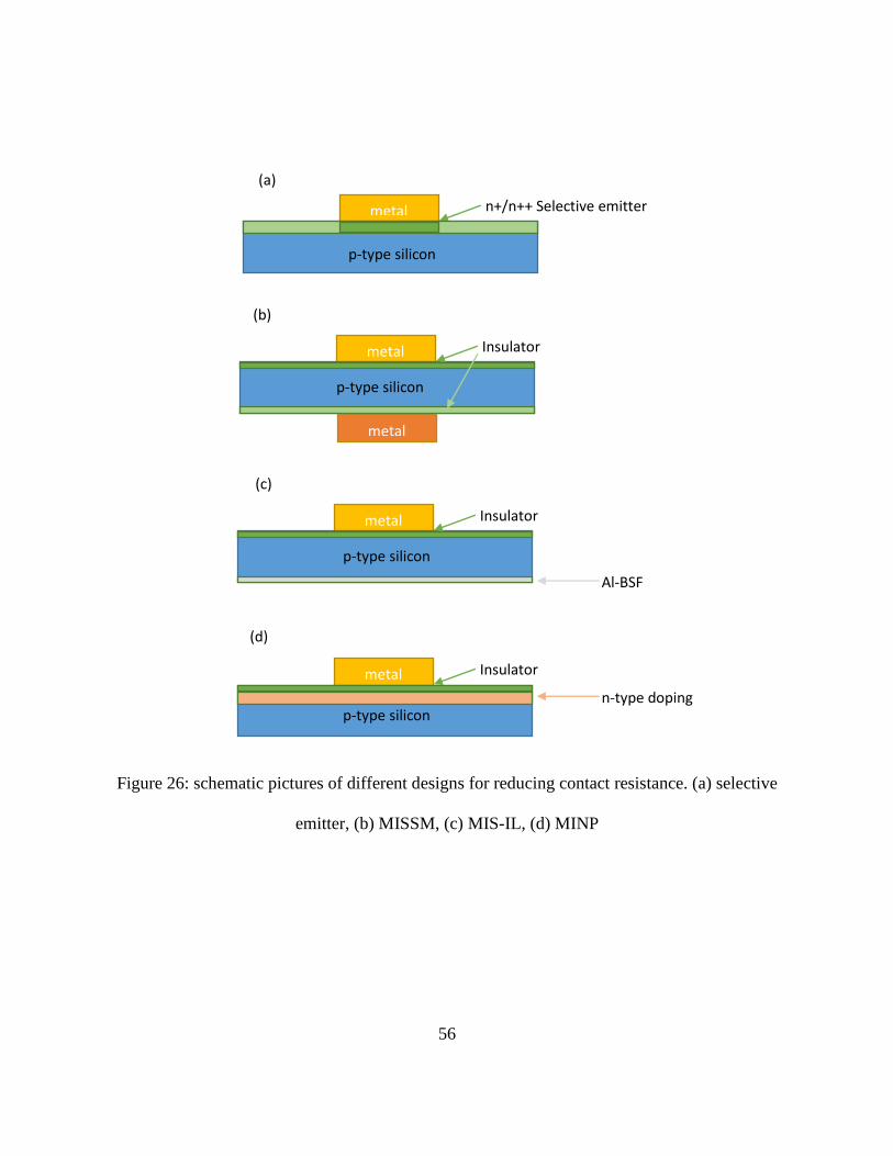
5.1 Methods of Reducing Contact Resistance
the intimate metal-silicon contact leads to recombination losses due to a high density of states at
the metal-silicon interface[24]. The selective emitter is a commonly used way to drastically
lowering contact resistance. The design uses high-temperature functional-impurity doping beneath
the metal terminal to achieve it. But this absorber doping induces its own fundamental energy
losses like Auger recombination, bandgap narrowing, and free-carrier absorption to limit the
device performance[25-28]. Due to these inherent limitations, the concept of passivating contacts
was introduced[24]. A passivation thin film inserted between the silicon wafer and the metal
terminal, physically separate them to prevent the recombination loss of direct contact but thin
enough to allow current flows. The early approach of passivating contact took the form of metal-
55
insulator-semiconductor(MIS) contacts[29]. A specific structure of metal-insulator-
semiconductor-insulator-metal(MISIM) was realized[70] with good performance. It used two
different metals for electron and hole collection and a film of silicon oxide as the insulator layer.
The lack of choice for affordable, high-work-function metals limits the application of such
structure. The MIS inversion layer(MIS-IL)structure solves the issue by forming a front MIS
contact on a p-type cell with an Al-BSF hole contact. The MIS contact was formed by thermally
evaporated Al and thin film of thermally grown SiO2[71]. Another design is the metal-insulator-
NP junction (MINP) concept. It formed MIS contact on a dopant-diffused surface, looking for the
benefits of reduced recombination velocity[72]. Different metals and insulators are studied using
the MINP structure for both n-type and p-type silicon cells[31, 32].
56
Figure 26: schematic pictures of different designs for reducing contact resistance. (a) selective
emitter, (b) MISSM, (c) MIS-IL, (d) MINP
n+/n++ Selective emitter metal
p-type silicon
(a)
Insulator metal
p-type silicon
metal
(b)
Al-BSF
Insulator metal
p-type silicon
(c)
n-type doping
Insulator metal
p-type silicon
(d)
57
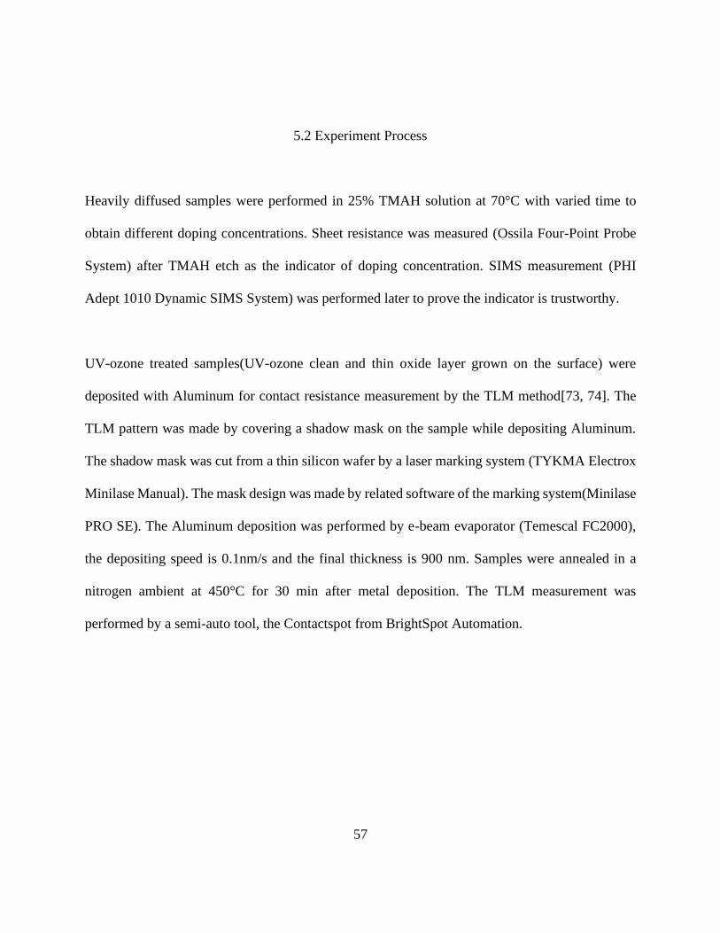
5.2 Experiment Process
Heavily diffused samples were performed in 25% TMAH solution at 70°C with varied time to
obtain different doping concentrations. Sheet resistance was measured (Ossila Four-Point Probe
System) after TMAH etch as the indicator of doping concentration. SIMS measurement (PHI
Adept 1010 Dynamic SIMS System) was performed later to prove the indicator is trustworthy.
UV-ozone treated samples(UV-ozone clean and thin oxide layer grown on the surface) were
deposited with Aluminum for contact resistance measurement by the TLM method[73, 74]. The
TLM pattern was made by covering a shadow mask on the sample while depositing Aluminum.
The shadow mask was cut from a thin silicon wafer by a laser marking system (TYKMA Electrox
Minilase Manual). The mask design was made by related software of the marking system(Minilase
PRO SE). The Aluminum deposition was performed by e-beam evaporator (Temescal FC2000),
the depositing speed is 0.1nm/s and the final thickness is 900 nm. Samples were annealed in a
nitrogen ambient at 450°C for 30 min after metal deposition. The TLM measurement was
performed by a semi-auto tool, the Contactspot from BrightSpot Automation.
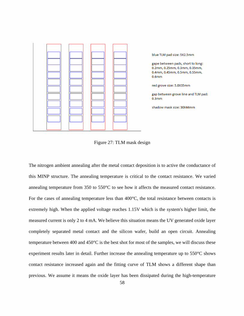
58
Figure 27: TLM mask design
The nitrogen ambient annealing after the metal contact deposition is to active the conductance of
this MINP structure. The annealing temperature is critical to the contact resistance. We varied
annealing temperature from 350 to 550°C to see how it affects the measured contact resistance.
For the cases of annealing temperature less than 400°C, the total resistance between contacts is
extremely high. When the applied voltage reaches 1.15V which is the system's higher limit, the
measured current is only 2 to 4 mA. We believe this situation means the UV generated oxide layer
completely separated metal contact and the silicon wafer, build an open circuit. Annealing
temperature between 400 and 450°C is the best shot for most of the samples, we will discuss these
experiment results later in detail. Further increase the annealing temperature up to 550°C shows
contact resistance increased again and the fitting curve of TLM shows a different shape than
previous. We assume it means the oxide layer has been dissipated during the high-temperature

59
annealing, turned the contact structure into a simple metal-semiconductor interface. We did not try
higher annealing temperature as the melting point of aluminum is 660°C. Based on these
experiments, we decided 450°C as the optimized annealing temperature and keep using it in all the
experiments.
60
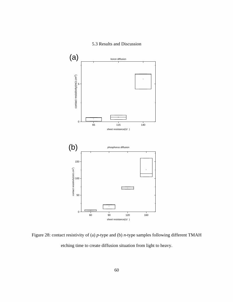
5.3 Results and Discussion
65 115 140
0
5
sheet resistance(W/ )
conta
ct
resis
itiv
ity(m
W.c
m2)
boron diffusion(a)
60 90 120 160
0
50
100
150
sheet resistance(W/ )
conta
ct re
sis
tivity(m
W.c
m2)
phosphorus diffusion(b)
Figure 28: contact resistivity of (a) p-type and (b) n-type samples following different TMAH
etching time to create diffusion situation from light to heavy.
61
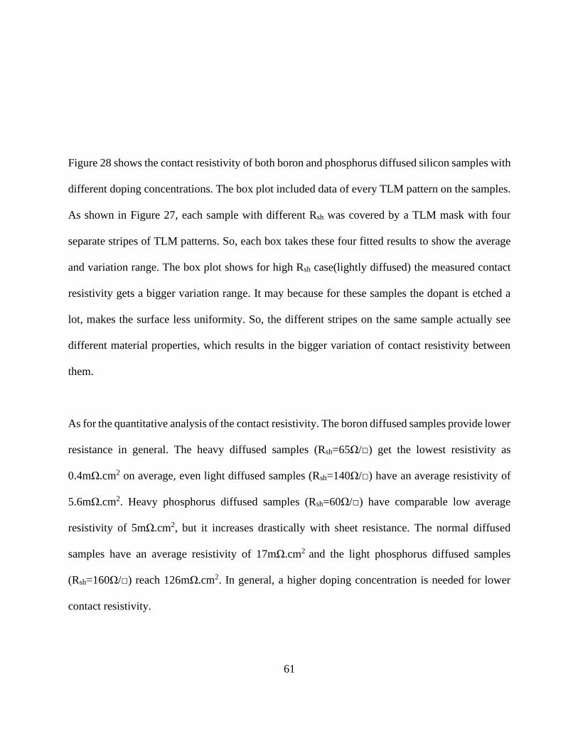
Figure 28 shows the contact resistivity of both boron and phosphorus diffused silicon samples with
different doping concentrations. The box plot included data of every TLM pattern on the samples.
As shown in Figure 27, each sample with different Rsh was covered by a TLM mask with four
separate stripes of TLM patterns. So, each box takes these four fitted results to show the average
and variation range. The box plot shows for high Rsh case(lightly diffused) the measured contact
resistivity gets a bigger variation range. It may because for these samples the dopant is etched a
lot, makes the surface less uniformity. So, the different stripes on the same sample actually see
different material properties, which results in the bigger variation of contact resistivity between
them.
As for the quantitative analysis of the contact resistivity. The boron diffused samples provide lower
resistance in general. The heavy diffused samples (Rsh=65Ω/□) get the lowest resistivity as
0.4mΩ.cm2 on average, even light diffused samples (Rsh=140Ω/□) have an average resistivity of
5.6mΩ.cm2. Heavy phosphorus diffused samples (Rsh=60Ω/□) have comparable low average
resistivity of 5mΩ.cm2, but it increases drastically with sheet resistance. The normal diffused
samples have an average resistivity of 17mΩ.cm2 and the light phosphorus diffused samples
(Rsh=160Ω/□) reach 126mΩ.cm2. In general, a higher doping concentration is needed for lower
contact resistivity.
62
But higher doping concentration not always means better. As we have already proved in the
previous chapter, higher doping concentration means more carriers on the wafer surface and will
result in a shorter lifetime. On the other hand, a lightly diffused wafer sacrifices contact resistivity
and surface uniformity for a longer carrier lifetime. Clearly, there is a trade-off between these
parameters for the good performance of the cell. In practice, the Rsh around 100Ω/□ is considered
a moderate diffused case with balanced and good performance.
63
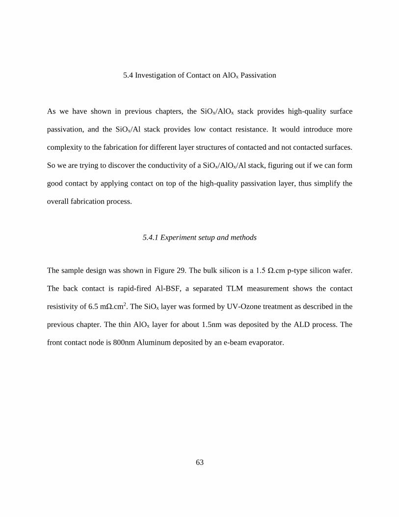
5.4 Investigation of Contact on AlOx Passivation
As we have shown in previous chapters, the SiOx/AlOx stack provides high-quality surface
passivation, and the SiOx/Al stack provides low contact resistance. It would introduce more
complexity to the fabrication for different layer structures of contacted and not contacted surfaces.
So we are trying to discover the conductivity of a SiOx/AlOx/Al stack, figuring out if we can form
good contact by applying contact on top of the high-quality passivation layer, thus simplify the
overall fabrication process.
5.4.1 Experiment setup and methods
The sample design was shown in Figure 29. The bulk silicon is a 1.5 Ω.cm p-type silicon wafer.
The back contact is rapid-fired Al-BSF, a separated TLM measurement shows the contact
resistivity of 6.5 mΩ.cm2. The SiOx layer was formed by UV-Ozone treatment as described in the
previous chapter. The thin AlOx layer for about 1.5nm was deposited by the ALD process. The
front contact node is 800nm Aluminum deposited by an e-beam evaporator.
64
Figure 29: structure scheme of the experiment sample
The possible carrier transport in the sample can be cataloged as several types. Tunneling is one of
the major effects that might happen under a high field. The tunnel emission is a result of the
quantum mechanic that allows electron wave function to penetrate a potential barrier. It can happen
for direct tunneling that penetrates the whole width of the potential barrier or Fowler-Nordheim
tunneling that tunnel through a partial width of the barrier.[75] For both cases, the process is highly
dependent on the applied voltage and independent of temperature.
Thermionic emission is another process of carrier transport. The electron gets enough kinetic
energy from heating to overcome the potential barrier. As the name indicated, the process is highly
dependent on temperature.
The Frenkel-Poole emission is also a possible type of carrier transport.[76] The trapped electrons
were emitted into the conduction band due to thermal excitation. For trap states with Coulomb
potentials, the expression is similar to thermionic emission while the barrier height is replaced by
the depth of trap potential well.
65
With low voltage and high temperature, the carrier transport can be the form of electrons hopping
from one isolated state to another. This mechanism will result in an ohmic characteristic behavior.
The space-charge-limited current occurs when carriers injected into a material with no
compensating charge presented, such as lightly doped semiconductor or insulator. For this unipolar
trap-free case the current is proportional to the square of the applied voltage.
For a given structure, these processes may not exactly independent from each other, and different
processes may dominate the carrier transport at a certain temperature and voltage range. Table 1
listed the basic types of carrier transport processes and their dependence on voltage and
temperature. The experiment sample was measured I-V curve at different temperatures. By fitting
the I-V curve and I-T curve with different dependence expressions, we can get an understanding
of which process is the most possible dominant process.
Table 1: Basic carrier transport types
Process Voltage and temperature dependence
Tunneling 𝐽 ∝ 𝑉2 𝑒−
𝑏𝑉
Thermionic emission 𝐽 ∝ 𝑇2𝑒𝑞𝑘𝑇
(𝑎√𝑉−𝜙𝐵)
Frenkel-Poole emission 𝐽 ∝ 𝑉𝑒𝑞𝑘𝑇
(2𝑎√𝑉−𝜙𝐵)
Ohmic 𝐽 ∝ 𝑉 𝑒−𝑐𝑇
Space-charge-limited 𝐽 ∝ 𝑉2
66
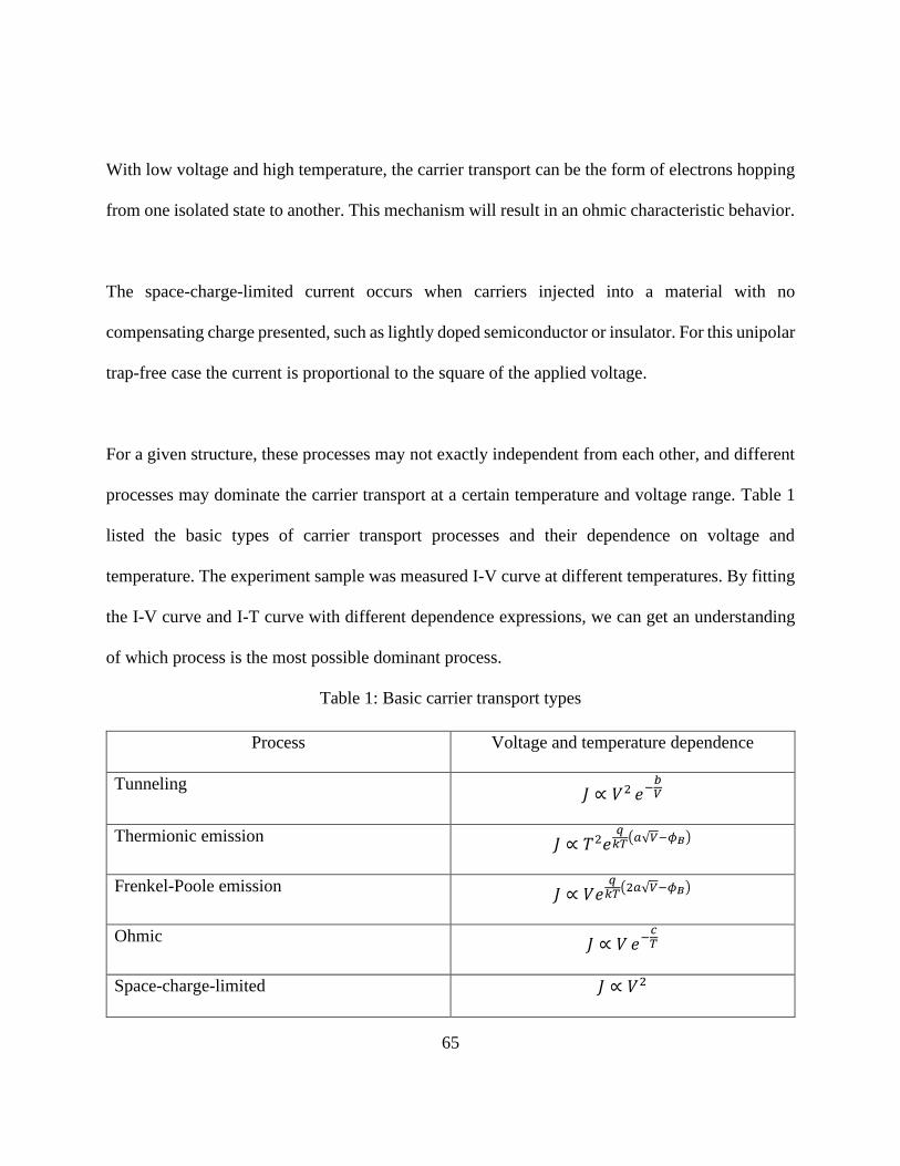
5.4.2 Experiment Results and Discussion
The sample’s I-V curve was measured by a MDC CSM/Win Semiconductor Measurement System.
The temperature was controlled by a Instec mK2000 precision temperature controller. Figure 30
shows the measured I-V curve of the as-deposited sample at different temperatures. As the figure
shows, the sample does not have a good conductance. The maximum current is less than 0.2mA.
Further fitting shows the curves match thermionic emission type and space-limited-charge type
well. We believe both mechanics contribute to carrier transport as the curve varies along with the
temperature but not as the thermionic emission type predicted. Either way, the carrier does not
transport through direct contact, makes conductivity high.
0.0 0.1 0.2 0.3 0.4 0.5
0.0
5.0x10⁻⁶
1.0x10⁻⁵
1.5x10⁻⁵
2.0x10⁻⁵
curr
ent (A
)
voltage (V)
25C
75C
100C
125C
150C
175C
Figure 30: I-V curve of the sample measured at different temperature
67
0.00 0.05 0.10 0.15 0.20 0.25
0.0
5.0x10⁻⁶
1.0x10⁻⁵
1.5x10⁻⁵
2.0x10⁻⁵
Curr
ent (A
)
Square of voltage (V2)
25C
75C
100C
125C
150C
175C
0.0 0.1 0.2 0.3 0.4 0.5 0.6 0.7 0.8
0.0
5.0x10⁻⁶
1.0x10⁻⁵
1.5x10⁻⁵
2.0x10⁻⁵
Cu
rre
nt
(A)
Square root of voltage (V1/2)
25C
75C
100C
125C
150C
175C
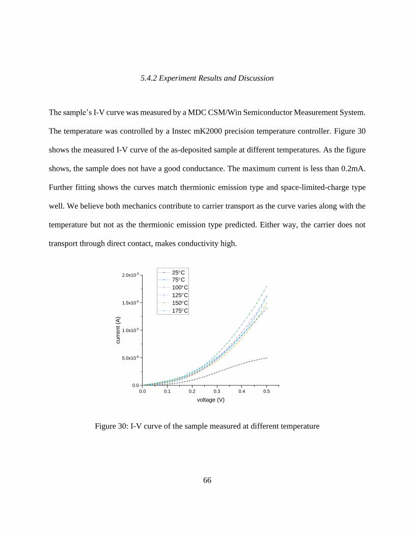
Figure 31: the fitting curve of space-limited-charge relation(upper) and thermionic emission
relation(lower)
We also investigate the sample after annealing. The sample was annealed in a nitrogen ambient at
450°C for 30 minutes. We chose this anneal process because it is the standard annealing situation
to activate the AlOx passivation in our previous experiment.
68
0.0 0.1 0.2 0.3 0.4 0.5
0.000
0.002
0.004
0.006
0.008
Curr
ent (A
)
Voltage (V)
25C
75C
100C
125C
150C
175C
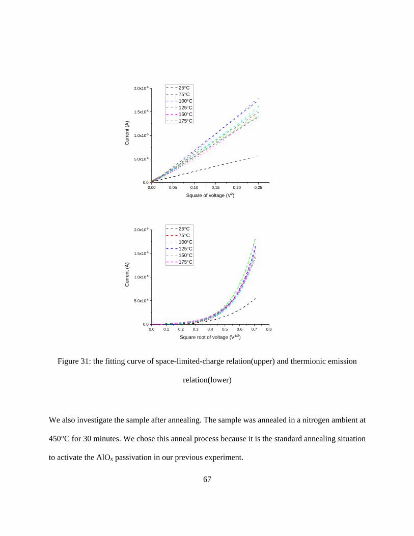
Figure 32: I-V curve of the annealed sample measured at different temperature
Figure 32 shows the I-V curve of the sample after annealing. Comparing to the result before
annealing, the conductance improved significantly. The measured current easily reached the higher
limit of the measurement system which is 0.01A. It also worth mention that the type of carrier
transport also changes, as the annealed I-V curve shows a linear relationship between current and
voltage, attributed to the ohmic type transport. It remains further investigation to figure out the
structural mechanic behind the low conductivity ohmic contact.
69
5.5 Summary
We built a MINP structure for both n-type(MIPN for n-type in fact) and p-type silicon wafer
substrate. The experiment results show Boron doped sample has less contact resistivity than
Phosphorus doped one in general. Higher doping concentration will generate lower contact
resistivity for both doping situations. But there are trade-offs between other properties to improve
cell performance in the end. A combination of passivating contact and AlOx passivation shows a
low conductance without annealing but greatly improved after annealed in a nitrogen ambient at
450°C for 30 minutes. The detailed carrier mechanic behind it remains unclear and needs further
investigation.
70
CHAPTER 6: SIMULATION OF THE CELLS
In the above chapters, we applied UV-Ozone treatment for different processes of fabricating the
solar cell. The results proved such treatment made contributions to higher quality in each step. But
for the solar cell as a device, all the processes are aiming for one goal at last: higher power
conversion efficiency. we would like to make real cells with UV-Ozone treatment involved but the
project and time schedule limited our ability. In this chapter, we will simulate the solar cell with
experimental parameters, and discuss how these different parameters affect the final efficiency of
the cell.
6.1 Simulation Methods and Setup
The optical simulation was done by Sunsolve, which combines ray tracing with thin-film wave
optics. The program sets a number of rays, each assigned a wavelength, intensity, and direction.
They are traced as a straight line until hit an interface between different materials. The interaction
was calculated as thin-film wave optics to determine absorptance, reflectance, and transmittance.
Thus, decided the intensity and direction of the next step ray trace. Such loop of calculation
repeated until 1) the ray either reflected from the front surface or transmitted through the rear
surface of the simulated module, or 2) the ray’s intensity decreased lower than a threshold, or 3)
the ray has reached the maximum interaction count. In the end, the gains and losses are recorded
for each ray and averaged to give the result used in the further simulation. The simulation’s
71
accuracy can be improved by applying more rays, lower intensity threshold, and higher interaction
count cap. Through optical simulation, we discussed how to optimize the interface stack on a
silicon wafer to maximize the electron generation.
The 3D device simulation of solar cells was performed with Quokka[77], based on the conductive
boundary approach[78]. The program numerically solves 3D steady-state charge carrier transport
in a quasi-neutral silicon device to figure out parameters of the device’s performance. The near-
surface regions are modeled by several decisive parameters like sheet resistance and effective
recombination characteristics rather than detailed doping profile and surface recombination. Thus
the simulation can be performed quickly without losing accuracy. All input simulation parameters
are determined experimentally, PCD measurement for J0 values, four-point probe measurement
for Rsh values, and TLM measurement for Rc values. The generation file was acquired from the
Sunsolve simulation as described above.
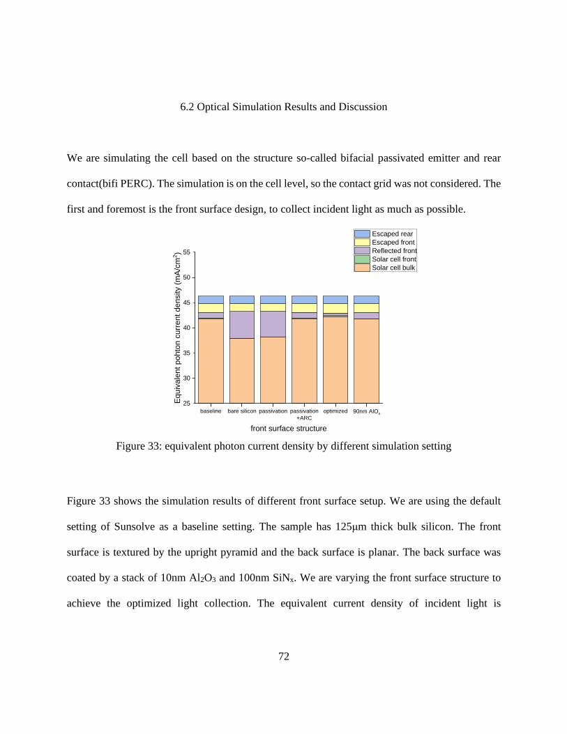
72
6.2 Optical Simulation Results and Discussion
We are simulating the cell based on the structure so-called bifacial passivated emitter and rear
contact(bifi PERC). The simulation is on the cell level, so the contact grid was not considered. The
first and foremost is the front surface design, to collect incident light as much as possible.
baseline bare silicon passivation passivation
+ARC
optimized 90nm AlOx
25
35
45
55
30
40
50
Equiv
ale
nt pohto
n c
urr
ent density (
mA
/cm
2)
front surface structure
Escaped rear
Escaped front
Reflected front
Solar cell front
Solar cell bulk
Figure 33: equivalent photon current density by different simulation setting
Figure 33 shows the simulation results of different front surface setup. We are using the default
setting of Sunsolve as a baseline setting. The sample has 125μm thick bulk silicon. The front
surface is textured by the upright pyramid and the back surface is planar. The back surface was
coated by a stack of 10nm Al2O3 and 100nm SiNx. We are varying the front surface structure to
achieve the optimized light collection. The equivalent current density of incident light is
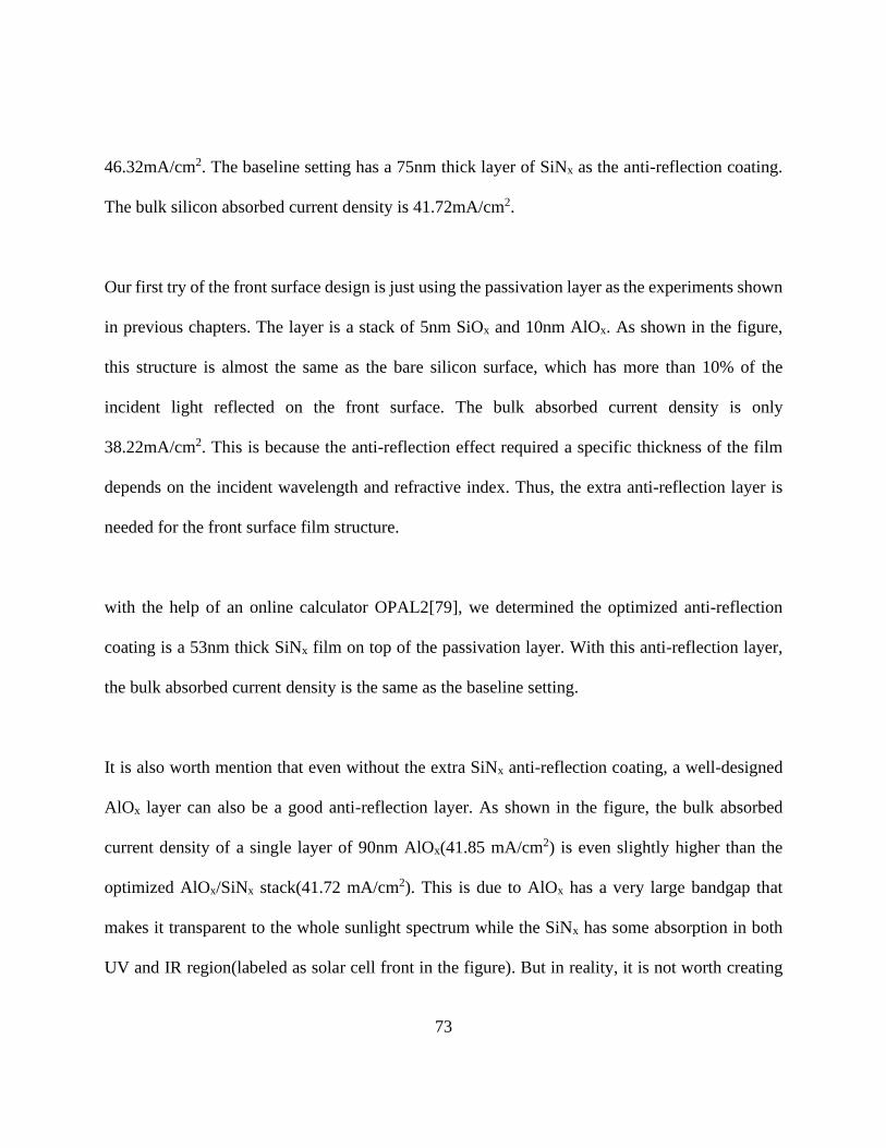
73
46.32mA/cm2. The baseline setting has a 75nm thick layer of SiNx as the anti-reflection coating.
The bulk silicon absorbed current density is 41.72mA/cm2.
Our first try of the front surface design is just using the passivation layer as the experiments shown
in previous chapters. The layer is a stack of 5nm SiOx and 10nm AlOx. As shown in the figure,
this structure is almost the same as the bare silicon surface, which has more than 10% of the
incident light reflected on the front surface. The bulk absorbed current density is only
38.22mA/cm2. This is because the anti-reflection effect required a specific thickness of the film
depends on the incident wavelength and refractive index. Thus, the extra anti-reflection layer is
needed for the front surface film structure.
with the help of an online calculator OPAL2[79], we determined the optimized anti-reflection
coating is a 53nm thick SiNx film on top of the passivation layer. With this anti-reflection layer,
the bulk absorbed current density is the same as the baseline setting.
It is also worth mention that even without the extra SiNx anti-reflection coating, a well-designed
AlOx layer can also be a good anti-reflection layer. As shown in the figure, the bulk absorbed
current density of a single layer of 90nm AlOx(41.85 mA/cm2) is even slightly higher than the
optimized AlOx/SiNx stack(41.72 mA/cm2). This is due to AlOx has a very large bandgap that
makes it transparent to the whole sunlight spectrum while the SiNx has some absorption in both
UV and IR region(labeled as solar cell front in the figure). But in reality, it is not worth creating
74
such a thick layer of AlOx for merely less than 1% improvement of the bulk absorption so we
won’t consider this structure in the future simulation.
We can further improve the bulk absorption by applying a more complex structure.[80] Adding
another SiOx film on top of SiNx will further decrease the front surface reflection. The optimized
design is 5nm SiOx/10nm AlOx/39nm SiNx/98nm SiOx. The simulation of this structure shows
only 1% of the incident light was reflected and the bulk absorption achieved 42.26 mA/cm2. That
is why we labeled it as optimized and will use the generation file from this design in future
simulations.
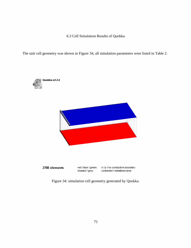
75
6.3 Cell Simulation Results of Quokka
The unit cell geometry was shown in Figure 34, all simulation parameters were listed in Table 2.
Figure 34: simulation cell geometry generated by Quokka.
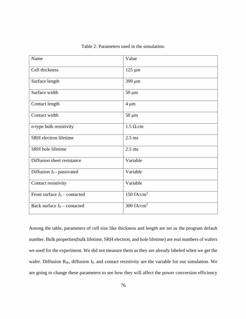
76
Table 2: Parameters used in the simulation.
Name Value
Cell thickness 125 μm
Surface length 399 μm
Surface width 50 μm
Contact length 4 μm
Contact width 50 μm
n-type bulk resistivity 1.5 Ω.cm
SRH electron lifetime 2.5 ms
SRH hole lifetime 2.5 ms
Diffusion sheet resistance Variable
Diffusion J0 - passivated Variable
Contact resistivity Variable
Front surface J0 – contacted 150 fA/cm2
Back surface J0 – contacted 300 fA/cm2
Among the table, parameters of cell size like thickness and length are set as the program default
number. Bulk properties(bulk lifetime, SRH electron, and hole lifetime) are real numbers of wafers
we used for the experiment. We did not measure them as they are already labeled when we get the
wafer. Diffusion Rsh, diffusion J0, and contact resistivity are the variable for our simulation. We
are going to change these parameters to see how they will affect the power conversion efficiency
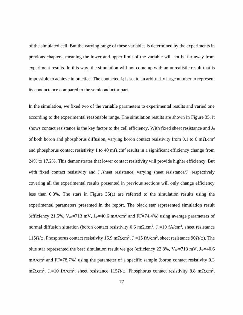
77
of the simulated cell. But the varying range of these variables is determined by the experiments in
previous chapters, meaning the lower and upper limit of the variable will not be far away from
experiment results. In this way, the simulation will not come up with an unrealistic result that is
impossible to achieve in practice. The contacted J0 is set to an arbitrarily large number to represent
its conductance compared to the semiconductor part.
In the simulation, we fixed two of the variable parameters to experimental results and varied one
according to the experimental reasonable range. The simulation results are shown in Figure 35, it
shows contact resistance is the key factor to the cell efficiency. With fixed sheet resistance and J0
of both boron and phosphorus diffusion, varying boron contact resistivity from 0.1 to 6 mΩ.cm2
and phosphorus contact resistivity 1 to 40 mΩ.cm2 results in a significant efficiency change from
24% to 17.2%. This demonstrates that lower contact resistivity will provide higher efficiency. But
with fixed contact resistivity and J0/sheet resistance, varying sheet resistance/J0 respectively
covering all the experimental results presented in previous sections will only change efficiency
less than 0.3%. The stars in Figure 35(a) are referred to the simulation results using the
experimental parameters presented in the report. The black star represented simulation result
(efficiency 21.5%, Voc=713 mV, Jsc=40.6 mA/cm2 and FF=74.4%) using average parameters of
normal diffusion situation (boron contact resistivity 0.6 mΩ.cm2, J0=10 fA/cm2, sheet resistance
115Ω/□. Phosphorus contact resistivity 16.9 mΩ.cm2, J0=15 fA/cm2, sheet resistance 90Ω/□). The
blue star represented the best simulation result we got (efficiency 22.8%, Voc=713 mV, Jsc=40.6
mA/cm2 and FF=78.7%) using the parameter of a specific sample (boron contact resistivity 0.3
mΩ.cm2, J0=10 fA/cm2, sheet resistance 115Ω/□. Phosphorus contact resistivity 8.8 mΩ.cm2,

78
J0=15 fA/cm2, sheet resistance 90Ω/□) in our experiment within the reasonable normal diffusion
situation.
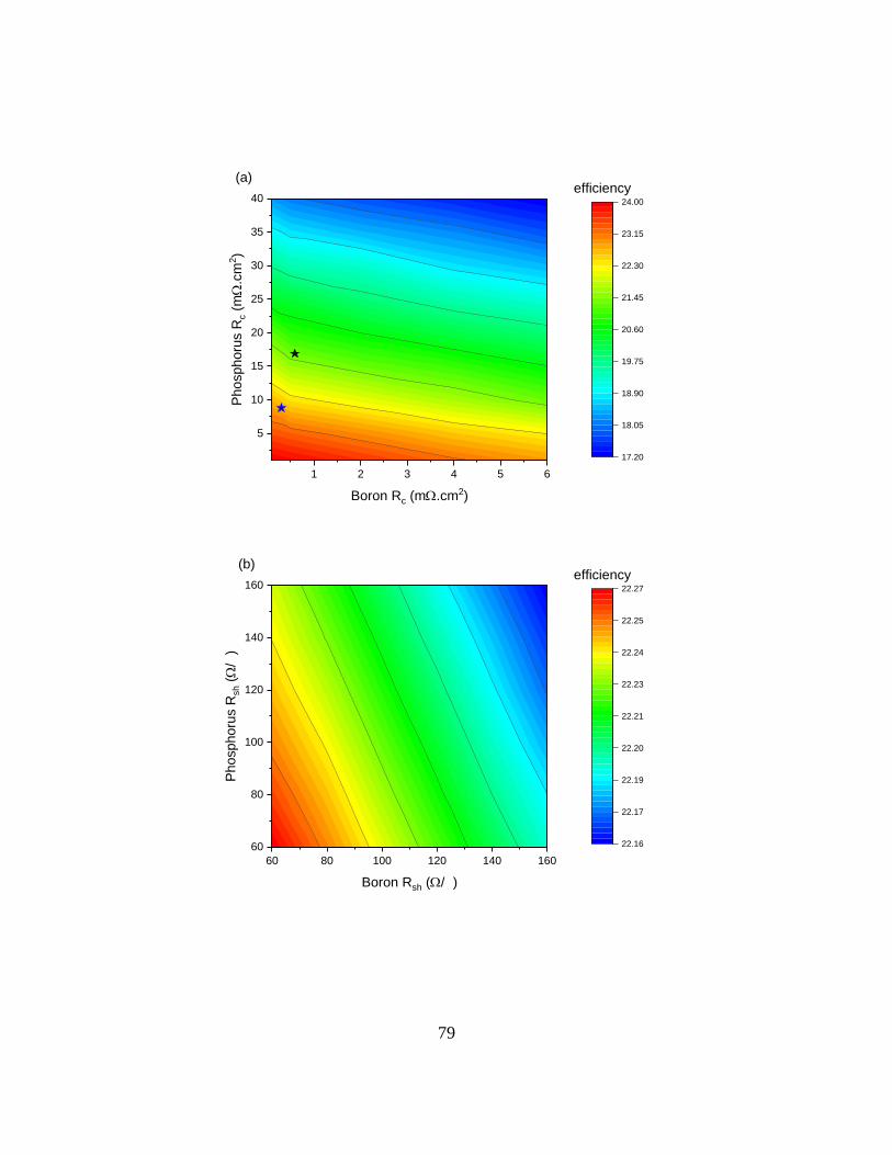
79
1 2 3 4 5 6
5
10
15
20
25
30
35
40
Ph
osph
oru
s R
c (
mW
.cm
2)
Boron Rc (mW.cm2)
17.20
18.05
18.90
19.75
20.60
21.45
22.30
23.15
24.00
efficiency(a)
60 80 100 120 140 160
60
80
100
120
140
160
Ph
osph
oru
s R
sh (
W/
)
Boron Rsh (W/ )
22.16
22.17
22.19
22.20
22.21
22.23
22.24
22.25
22.27
efficiency(b)
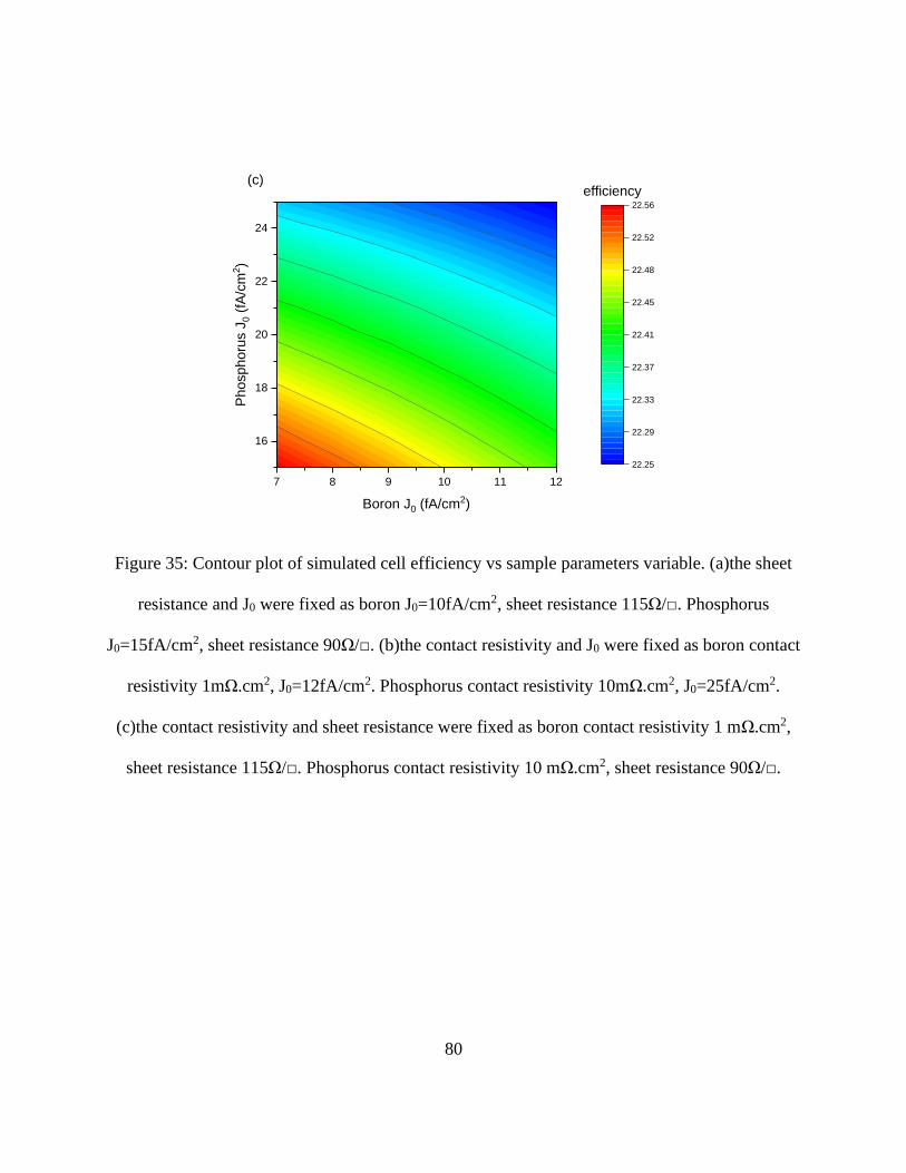
80
7 8 9 10 11 12
16
18
20
22
24P
ho
sph
oru
s J
0 (
fA/c
m2)
Boron J0 (fA/cm2)
22.25
22.29
22.33
22.37
22.41
22.45
22.48
22.52
22.56
efficiency(c)
Figure 35: Contour plot of simulated cell efficiency vs sample parameters variable. (a)the sheet
resistance and J0 were fixed as boron J0=10fA/cm2, sheet resistance 115Ω/□. Phosphorus
J0=15fA/cm2, sheet resistance 90Ω/□. (b)the contact resistivity and J0 were fixed as boron contact
resistivity 1mΩ.cm2, J0=12fA/cm2. Phosphorus contact resistivity 10mΩ.cm2, J0=25fA/cm2.
(c)the contact resistivity and sheet resistance were fixed as boron contact resistivity 1 mΩ.cm2,
sheet resistance 115Ω/□. Phosphorus contact resistivity 10 mΩ.cm2, sheet resistance 90Ω/□.
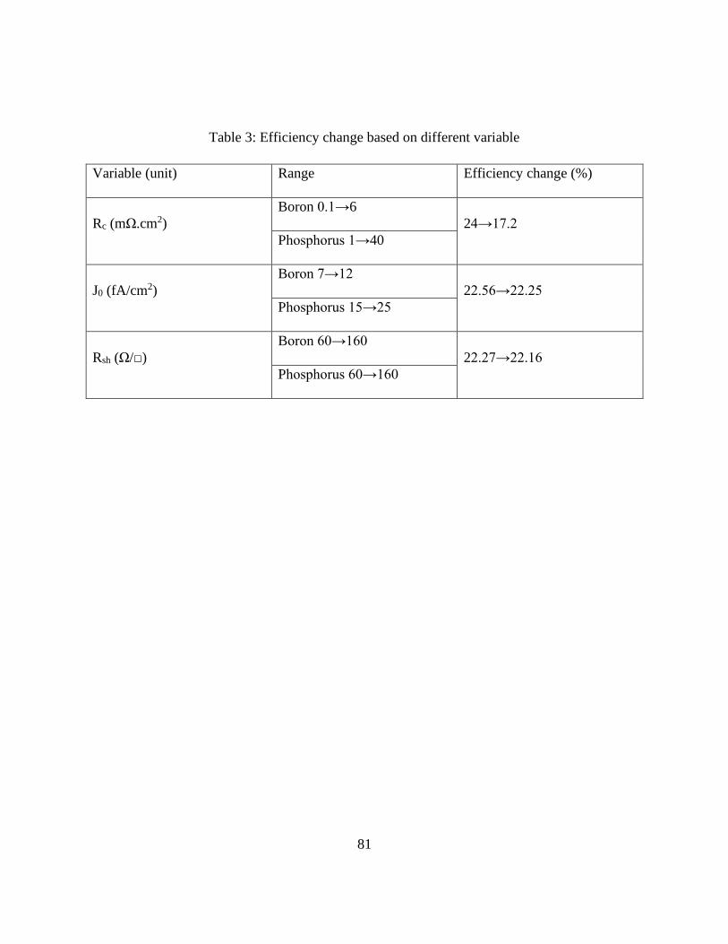
81
Table 3: Efficiency change based on different variable
Variable (unit) Range Efficiency change (%)
Rc (mΩ.cm2)
Boron 0.1→6
24→17.2
Phosphorus 1→40
J0 (fA/cm2)
Boron 7→12
22.56→22.25
Phosphorus 15→25
Rsh (Ω/□)
Boron 60→160
22.27→22.16
Phosphorus 60→160
82
6.4 Summary
We have simulated the performance of a solar cell based on the experimentally acquired
parameters. The simulation results showed a trade-off between parameters as we expected. Lower
contact resistivity leads to higher cell efficiency, which can be achieved by increasing doping
concentration. Lower J0 also leads to higher cell efficiency, which can be achieved by decreasing
doping concentration. Increasing doping concentration itself for a lower Rsh can increase efficiency,
too. Within the range of moderate doping situation, contact resistivity shows a dominating effect
on power conversion efficiency comparing to J0 and Rsh. The simulation results suggest aiming for
a heavier doped design to achieve higher efficiency of solar cells.
83
CHAPTER 7: SUMMARY AND CONCLUSION
We have demonstrated the effective use of UV-ozone treatment in multiple silicon solar cell
fabrication processes:
1) a surface cleaning method providing comparable cleaning quality to the industrial standard
RCA clean. Both methods can reduce the surface recombination current density J0 down
to less than 10fA/cm2. Repeating treatment can further improve the cleaning quality by 15-
20% each time.
2) in combination with ALD aluminum oxide, a passivation stack providing high passivation
quality for both n-type and p-type silicon. The thicker oxide layer made by UV-ozone
treatment can reduce J0 up to 25% and nearly double the effective lifetime.
3) an MIS contact structure with low contact resistivity on both n-type and p-type silicon. The
p-type samples get a generally better result for contact resistivity as low as 0.6mΩ.cm2
while n-type samples get the lowest contact resistivity of 16.9mΩ.cm2. The contact on AlOx
also shows good conductance after the annealing process.
Combining experimental results in the processes mentioned above, Quokka simulation predicted
promising high cell efficiency and indicated reducing contact resistivity is a key factor for reaching
higher efficiency.
84
LIST OF REFERENCE
[1] Chodos, A., April 25, 1954: Bell Labs Demonstrates the First Practical Silicon Solar Cell.
APS News-This month in Physics history, 2009.
[2] Blakers, A.W. and M.A. Green, 20% efficiency silicon solar cells. Applied Physics Letters,
1986. 48(3): p. 215-217.
[3] Dimroth, F., W. Guter, J. Schöne, E. Welser, M. Steiner, E. Oliva, A. Wekkeli, G. Siefer, S.
Philipps, and A. Bett. Metamorphic GaInP/GaInAs/Ge triple-junction solar cells with≫
41% efficiency. in 2009 34th IEEE Photovoltaic Specialists Conference (PVSC). 2009.
IEEE.
[4] Fthenakis, V.M., Life cycle impact analysis of cadmium in CdTe PV production. Renewable
and Sustainable Energy Reviews, 2004. 8(4): p. 303-334.
[5] Yablonovitch, E., O.D. Miller, and S. Kurtz. The opto-electronic physics that broke the
efficiency limit in solar cells. in 2012 38th IEEE photovoltaic specialists conference. 2012.
IEEE.
[6] Oku, T., K. Kumada, A. Suzuki, and K. Kikuchi, Effects of germanium addition to copper
phthalocyanine/fullerene-based solar cells, in Open Engineering. 2012. p. 248.
[7] pveducation. Available from: https://www.pveducation.org/pvcdrom/solar-cell-
operation/solar-cell-structure.
[8] Kern, W., Cleaning Solution Based on Hydrogen Peroxide for Use in Silicon Semiconductor
Technology. RCA Review, 1970. 31: p. 187-205.
[9] Meuris, M., P. Mertens, A. Opdebeeck, H. Schmidt, M. Depas, G. Vereecke, M. Heyns, and
A. Philipossian, The IMEC clean: A new concept for particle and metal removal on Si
surfaces. Solid State Technology, 1995. 38(7): p. 109-113.
[10] Vossen, J., Glow discharge phenomena in plasma etching and plasma deposition. Journal of
the Electrochemical Society, 1979. 126(2): p. 319-324.
[11] McDermott, W.T., R.C. Ockovic, J.J. Wu, D.W. Cooper, A. Schwarz, and H.L. Wolfe,
Surface cleaning using a cryogenic aerosol. 1991, Google Patents.
[12] Vig, J.R., UV/ozone cleaning of surfaces. Journal of Vacuum Science & Technology A:
Vacuum, Surfaces, and Films, 1985. 3(3): p. 1027-1034.
[13] Baunack, S. and A. Zehe, A study of UV/Ozone cleaning procedure for silicon surfaces. 1989.
115(1): p. 223-227.
[14] Belay, A.B., W. Zhou, R. Krueger, K.O. Davis, Ü. Alver, and N. Sorloaica-Hickman, Effect
of UV-ozone exposure on PCBM. IEEE Journal of Photovoltaics, 2012. 2(2): p. 148-153.
[15] Zin, N., S. Bakhshi, M. Gao, H. Ali, I. Kashkoush, and W.V. Schoenfeld, Effective Use of
UV-Ozone Oxide in Silicon Solar Cell Applications. physica status solidi (RRL) – Rapid
Research Letters, 2019. 13(2): p. 1800488.
85
[16] Siemens, W., Ueber die elektrostatische Induction und die Verzögerung des Stroms in
Flaschendrähten. Annalen der Physik, 1857. 178(9): p. 66-122.
[17] Bonilla, R.S., B. Hoex, P. Hamer, and P.R. Wilshaw, Dielectric surface passivation for silicon
solar cells: A review. physica status solidi (a), 2017. 214(7): p. 1700293.
[18] Aberle, A.G., S. Glunz, and W. Warta, Impact of illumination level and oxide parameters on
Shockley–Read–Hall recombination at the Si‐SiO2 interface. Journal of Applied
Physics, 1992. 71(9): p. 4422-4431.
[19] Aberle, A.G., Overview on SiN surface passivation of crystalline silicon solar cells. Solar
energy materials and solar cells, 2001. 65(1-4): p. 239-248.
[20] Matsuura, H., T. Okuno, H. Okushi, and K. Tanaka, Electrical properties of n ‐amorphous/p‐ crystalline silicon heterojunctions. Journal of Applied Physics, 1984.
55(4): p. 1012-1019.
[21] Saint-Cast, P., J. Benick, D. Kania, L. Weiss, M. Hofmann, J. Rentsch, R. Preu, and S.W.
Glunz, High-efficiency c-Si solar cells passivated with ALD and PECVD aluminum oxide.
IEEE Electron Device Letters, 2010. 31(7): p. 695-697.
[22] Bakhshi, S., N. Zin, H. Ali, M. Wilson, D. Chanda, K.O. Davis, and W.V. Schoenfeld, Simple
and versatile UV-ozone oxide for silicon solar cell applications. Solar Energy Materials
and Solar Cells, 2018. 185: p. 505-510.
[23] Liao, B., B. Hoex, A.G. Aberle, D. Chi, and C.S. Bhatia, Excellent c-Si surface passivation
by low-temperature atomic layer deposited titanium oxide. Applied Physics Letters, 2014.
104(25): p. 253903.
[24] Allen, T.G., J. Bullock, X. Yang, A. Javey, and S. De Wolf, Passivating contacts for
crystalline silicon solar cells. Nature Energy, 2019: p. 1-15.
[25] Richter, A., S.W. Glunz, F. Werner, J. Schmidt, and A. Cuevas, Improved quantitative
description of Auger recombination in crystalline silicon. Physical Review B, 2012.
86(16): p. 165202.
[26] Yan, D. and A. Cuevas, Empirical determination of the energy band gap narrowing in highly
doped n+ silicon. Journal of Applied Physics, 2013. 114(4): p. 044508.
[27] Baker-Finch, S.C., K.R. McIntosh, D. Yan, K.C. Fong, and T.C. Kho, Near-infrared free
carrier absorption in heavily doped silicon. Journal of Applied Physics, 2014. 116(6): p.
063106.
[28] Yan, D. and A. Cuevas, Empirical determination of the energy band gap narrowing in p+
silicon heavily doped with boron. Journal of Applied Physics, 2014. 116(19): p. 194505.
[29] Green, M.A. and R. Godfrey, MIS solar cell—General theory and new experimental results
for silicon. Applied Physics Letters, 1976. 29(9): p. 610-612.
[30] Hezel, R. and R. Schörner, Plasma Si nitride—A promising dielectric to achieve high‐quality silicon MIS/IL solar cells. Journal of Applied Physics, 1981. 52(4): p. 3076-3079.
[31] Zielke, D., J.H. Petermann, F. Werner, B. Veith, R. Brendel, and J. Schmidt, Contact
passivation in silicon solar cells using atomic‐layer‐deposited aluminum oxide layers.
physica status solidi (RRL)–Rapid Research Letters, 2011. 5(8): p. 298-300.
86
[32] Bullock, J., A. Cuevas, C. Samundsett, D. Yan, J. McKeon, and Y. Wan, Simple silicon solar
cells featuring an a-Si: H enhanced rear MIS contact. Solar Energy Materials and Solar
Cells, 2015. 138: p. 22-25.
[33] Moldovan, A., F. Feldmann, G. Krugel, M. Zimmer, J. Rentsch, M. Hermle, A. Roth-Fölsch,
K. Kaufmann, and C. Hagendorf, Simple cleaning and conditioning of silicon surfaces with
UV/ozone sources. Energy Procedia, 2014. 55: p. 834-844.
[34] Johnson, R.W., A. Hultqvist, and S.F. Bent, A brief review of atomic layer deposition: from
fundamentals to applications. Materials today, 2014. 17(5): p. 236-246.
[35] Sinton, R.A. and A. Cuevas, Contactless determination of current–voltage characteristics
and minority ‐ carrier lifetimes in semiconductors from quasi ‐ steady ‐ state
photoconductance data. Applied Physics Letters, 1996. 69(17): p. 2510-2512.
[36] Cuevas, A., R.A. Sinton, and M. Stuckings. Determination of recombination parameters in
semiconductors from photoconductance measurements. in 1996 Conference on
Optoelectronic and Microelectronic Materials and Devices. Proceedings. 1996. IEEE.
[37] Seigneur, H., E.J. Schneller, N.S. Shiradkar, and W.V. Schoenfeld, Effect of Diamond Wire
Saw Marks on Solar Cell Performance. Energy Procedia, 2016. 92: p. 386-391.
[38] Park, H., S. Kwon, J.S. Lee, H.J. Lim, S. Yoon, and D. Kim, Improvement on surface texturing
of single crystalline silicon for solar cells by saw-damage etching using an acidic solution.
Solar Energy Materials and Solar Cells, 2009. 93(10): p. 1773-1778.
[39] Chen, G. The applications of DI-O3 water on wafer surface preparation. in International
Conference on Wafer Rinsing, Water Reclamation and Environmental Technology for
Semiconductor Manufacturing, Industrial Technology Research Institute, Hsinchu,
Taiwan. 1999.
[40] Moldovan, A., F. Feldmann, K. Kaufmann, S. Richter, M. Werner, C. Hagendorf, M. Zimmer,
J. Rentsch, and M. Hermle. Tunnel oxide passivated carrier-selective contacts based on
ultra-thin SiO2 layers grown by photo-oxidation or wet-chemical oxidation in ozonized
water. in 2015 IEEE 42nd Photovoltaic Specialist Conference (PVSC). 2015. IEEE.
[41] Ali, H., A. Moldovan, S. Mack, W.V. Schoenfeld, and K.O. Davis, Transmission electron
microscopy based interface analysis of the origin of the variation in surface recombination
of silicon for different surface preparation methods and passivation materials. physica
status solidi (a), 2017. 214(10): p. 1700286.
[42] Ali, H., A. Moldovan, S. Mack, M. Wilson, W.V. Schoenfeld, and K.O. Davis, Influence of
surface preparation and cleaning on the passivation of boron diffused silicon surfaces for
high efficiency photovoltaics. Thin Solid Films, 2017. 636: p. 412-418.
[43] S. Bakhshi, N.Z., K. Davis, M. Wilson, I. Kashkoush, W. Schoenfled, Improving silicon
surface passivation with a silicon oxide layer grown via ozonated deionized water, in
Proceedings of the 44th IEEE Photovoltaic Specialists Conference. 2017: Washington DC.
[44] Istratov, A.A., H. Hieslmair, and E.R. Weber, Iron contamination in silicon technology.
Applied Physics A, 2000. 70(5): p. 489-534.
[45] Chen, P.-Y., Characteristics of spontaneous reaction occurred by metal contamination and
silicon substrate for ultralarge-scale integration semiconductor process. Journal of The
Electrochemical Society, 2008. 155(9): p. H682-H687.
87
[46] Jian, S.-K.J., C.-C. Jeng, and W.S. Yoo, Monitoring metal contamination of silicon by
multiwavelength room temperature photoluminescence spectroscopy. AIP Advances,
2012. 2(4): p. 042164.
[47] Bolon, D. and C. Kunz, Ultraviolet depolymerization of photoresist polymers. Polymer
Engineering & Science, 1972. 12(2): p. 109-111.
[48] Vig, J. and J. LeBus, UV/Ozone Cleaning of Surfaces. IEEE Transactions on Parts, Hybrids,
and Packaging, 1976. 12(4): p. 365-370.
[49] Nakamura, K., T. Futatsuki, K. Makihara, and T. Ohmi. Ultra thin oxide formation using
chemical oxide passivation. in International Symposium on Cleaning Technological in
Semiconductor Device Manufacturing III, 1994, vol. Electrochemical Society Proceedings.
1994.
[50] Zhang, H. and J. Ouyang, High-efficiency inverted bulk heterojunction polymer solar cells
with UV ozone-treated ultrathin aluminum interlayer. Applied Physics Letters, 2010.
97(6): p. 063509.
[51] Xia, Y., Y. Pan, H. Zhang, J. Qiu, Y. Zheng, Y. Chen, and W. Huang, Graphene Oxide by
UV-Ozone Treatment as an Efficient Hole Extraction Layer for Highly Efficient and Stable
Polymer Solar Cells. ACS Applied Materials & Interfaces, 2017. 9(31): p. 26252-26256.
[52] Cheng, F., G. Fang, X. Fan, H. Huang, Q. Zheng, P. Qin, H. Lei, and Y. Li, Enhancing the
performance of P3HT: ICBA based polymer solar cells using LiF as electron collecting
buffer layer and UV–ozone treated MoO3 as hole collecting buffer layer. Solar Energy
Materials and Solar Cells, 2013. 110: p. 63-68.
[53] Turren-Cruz, S.-H., M. Saliba, M.T. Mayer, H. Juárez-Santiesteban, X. Mathew, L. Nienhaus,
W. Tress, M.P. Erodici, M.-J. Sher, M.G. Bawendi, M. Grätzel, A. Abate, A. Hagfeldt, and
J.-P. Correa-Baena, Enhanced charge carrier mobility and lifetime suppress hysteresis and
improve efficiency in planar perovskite solar cells. Energy & Environmental Science,
2018. 11(1): p. 78-86.
[54] Kogelschatz, U., B. Eliasson, and W. Egli, From ozone generators to flat television screens:
history and future potential of dielectric-barrier discharges, in Pure and Applied
Chemistry. 1999. p. 1819.
[55] Kogelschatz, U., Dielectric-barrier discharges: their history, discharge physics, and
industrial applications. Plasma chemistry and plasma processing, 2003. 23(1): p. 1-46.
[56] Sowell, R.R., R.E. Cuthrell, D.M. Mattox, and R.D. Bland, Surface cleaning by ultraviolet
radiation. Journal of Vacuum Science and Technology, 1974. 11(1): p. 474-475.
[57] Saint-Cast, P., D. Kania, M. Hofmann, J. Benick, J. Rentsch, and R. Preu, Very low surface
recombination velocity on p-type c-Si by high-rate plasma-deposited aluminum oxide.
Applied Physics Letters, 2009. 95(15): p. 151502.
[58] Aberle, A.G., Surface passivation of crystalline silicon solar cells: a review. Progress in
Photovoltaics: Research and Applications, 2000. 8(5): p. 473-487.
[59] Castro, P. and B. Deal, Low‐Temperature Reduction of Fast Surface States Associated with
Thermally Oxidized Silicon. Journal of the Electrochemical Society, 1971. 118(2): p. 280-
286.
88
[60] Aberle, A.G., T. Lauinger, J. Schmidt, and R. Hezel, Injection‐level dependent surface
recombination velocities at the silicon‐plasma silicon nitride interface. Applied physics
letters, 1995. 66(21): p. 2828-2830.
[61] Schmidt, J. and A.G. Aberle, Carrier recombination at silicon–silicon nitride interfaces
fabricated by plasma-enhanced chemical vapor deposition. Journal of Applied Physics,
1999. 85(7): p. 3626-3633.
[62] Kerr, M.J. and A. Cuevas, Recombination at the interface between silicon and stoichiometric
plasma silicon nitride. Semiconductor science and technology, 2002. 17(2): p. 166.
[63] Goodrich, A., P. Hacke, Q. Wang, B. Sopori, R. Margolis, T.L. James, and M. Woodhouse,
A wafer-based monocrystalline silicon photovoltaics road map: Utilizing known
technology improvement opportunities for further reductions in manufacturing costs. Solar
Energy Materials and Solar Cells, 2013. 114: p. 110-135.
[64] Larionova, Y., V. Mertens, N.-P. Harder, and R. Brendel, Surface passivation of n-type
Czochralski silicon substrates by thermal-SiO 2/plasma-enhanced chemical vapor
deposition SiN stacks. Applied physics letters, 2010. 96(3): p. 032105.
[65] Bonilla, R.S., F. Woodcock, and P.R. Wilshaw, Very low surface recombination velocity in
n-type c-Si using extrinsic field effect passivation. Journal of Applied Physics, 2014.
116(5): p. 054102.
[66] Hezel, R. and K. Jaeger, Low‐temperature surface passivation of silicon for solar cells.
Journal of the Electrochemical Society, 1989. 136(2): p. 518-523.
[67] König, D., M. Rennau, M. Henker, and G. Ebest, Evidence of a high density of fixed negative
charges in an insulation layer compound on silicon. Thin Solid Films, 2001. 385(1-2): p.
126-131.
[68] Small, C.E., S. Chen, J. Subbiah, C.M. Amb, S.-W. Tsang, T.-H. Lai, J.R. Reynolds, and F.
So, High-efficiency inverted dithienogermole–thienopyrrolodione-based polymer solar
cells. Nature Photonics, 2011. 6: p. 115.
[69] Trupke, T., R. Bardos, M. Abbott, P. Würfel, E. Pink, Y. Augarten, F. Chen, K. Fisher, J.E.
Cotter, and M. Kasemann, Progress with luminescence imaging for the characterisation of
silicon wafers and solar cells. Proceeding of the 22nd EPVSC, Milan, Italy, 2007.
[70] Tarr, N., D. Pulfrey, and P. Iles, Induced back‐surface field solar cells on p‐type silicon
substrates. Applied Physics Letters, 1981. 39(1): p. 83-85.
[71] Hezel, R., Recent progress in MIS solar cells. Progress in Photovoltaics: Research and
Applications, 1997. 5(2): p. 109-120.
[72] Blakers, A.W. and M.A. Green, 678‐mV open‐circuit voltage silicon solar cells. Applied
Physics Letters, 1981. 39(6): p. 483-485.
[73] Berger, H. Contact resistance on diffused resistors. in 1969 IEEE International Solid-State
Circuits Conference. Digest of Technical Papers. 1969. IEEE.
[74] Reeves, G. and H. Harrison, Obtaining the specific contact resistance from transmission line
model measurements. IEEE Electron device letters, 1982. 3(5): p. 111-113.
[75] Jensen, K.L., Electron emission theory and its application: Fowler–Nordheim equation and
beyond. Journal of Vacuum Science & Technology B: Microelectronics and Nanometer
Structures Processing, Measurement, and Phenomena, 2003. 21(4): p. 1528-1544.
89
[76] Takahashi, Y. and K. Ohnishi, Estimation of insulation layer conductance in MNOS structure.
IEEE Transactions on electron devices, 1993. 40(11): p. 2006-2010.
[77] Fell, A., A free and fast three-dimensional/two-dimensional solar cell simulator featuring
conductive boundary and quasi-neutrality approximations. IEEE Transactions on Electron
Devices, 2012. 60(2): p. 733-738.
[78] Brendel, R., Modeling solar cells with the dopant-diffused layers treated as conductive
boundaries. Progress in Photovoltaics: Research and Applications, 2012. 20(1): p. 31-43.
[79] OPAL2. Available from:
https://www2.pvlighthouse.com.au/calculators/OPAL%202/OPAL%202.aspx.
[80] Franklin, E., K. Fong, K. McIntosh, A. Fell, A. Blakers, T. Kho, D. Walter, D. Wang, N. Zin,
M. Stocks, E.-C. Wang, N. Grant, Y. Wan, Y. Yang, X. Zhang, Z. Feng, and P.J. Verlinden,
Design, fabrication and characterisation of a 24.4% efficient interdigitated back contact
solar cell. Progress in Photovoltaics: Research and Applications, 2016. 24(4): p. 411-427.