Embed Size (px)
Citation preview
ISSUE 1 2014 RADTECH REPORT 45
Tech
nica
l Pap
er
Ultraviolet (UV)-LEDs have
rapidly improved as they have
entered the commercial market,
with sales totalling $45 million out
of the total $495.4 million UV lamp
market in 2012.1 The majority of the
market is currently served by products
emitting in the UV-A wavelength
range, with curing being the largest
application. UV-C-LED technology is
improving rapidly as commercialization
has begun, with large markets in water
purification and disinfection driving
UV-C Light EmittingDiodesBy Craig Moe majority of the optoelectronics in
use today are constructed from
III-V materials.2 For example, the
mature technologies of lasers used
in fiber-optic communications are
fabricated from indium gallium
arsenide phosphide and are designed
with specific alloying ratios to emit
at wavelengths of 1.3 µm or 1.55 µm,
while the laser in a commercial DVD
player has an active region of gallium
indium phosphide and emits at 650 nm.
The nature of III-phosphide and
III-arsenide materials is such that
optoelectronic structures with alloys
of specific concentrations can be
designed so that the entire material
stack has the same crystal lattice
constant or spacing between atoms.
This, in conjunction with the ready
availability of near-perfect substrates
of gallium arsenide and indium
phosphide, allows for defect-free
optoelectronic devices to be produced.
Any defect in the crystal structure
is a point where electrical carriers
can recombine in a way that does not
produce the desired wavelength and,
thus, the efficiency is reduced. It is
because of these native substrates
and careful epitaxial growth of
optoelectronics that much of the
technology we use today is possible.
Up until the early 1990s, the
shortest wavelength, commercially
available III-V light-emitting diodes
were a weak green—suitable primarily
for telephone backlighting and
indicator lights. They were made from
aluminum gallium phosphide. It wasn’t
until Shuji Nakamura3 and others
UV-C LED technology is improving rapidly as commercialization has begun, with large markets in water purification and disinfection driving advances.
advances. This article discusses the
technology behind UV-LEDs and
how advances in the UV-C range can
complement longer wavelength curing
applications.
UV-LEDs are manufactured from a
class of materials referred to as III-V
semiconductors. These materials are
epitaxially grown into crystals with
a precise ratio of one atom from the
Group V column of the periodic table
to one atom from the Group III.
The smaller the atomic number of
the elements used, the more ionic
the character of the atomic bonds,
resulting in a smaller lattice constant
and larger electrical bandgap. This
bandgap determines the wavelength
at which a particular material will
emit light. This ability to tailor by
alloying and the fact that many III-V
semiconductors are direct bandgap
is responsible for the fact that the
46 RADTECH REPORT ISSUE 1 2014
Tech
nica
l Pap
er
successfully produced LEDs of indium
gallium nitride that blue and true green
LEDs (and later solid-state lasers) in
these wavelengths were realized.
Unlike their longer wavelength
counterparts, there were no native
substrates available to use in producing
these devices. Epitaxial structures
were instead produced on foreign
substrates, such as sapphire and
silicon carbide. Due to the large lattice
mismatch between these materials,
the resulting epitaxy had a large
number of defects, as many as 1010 per
square centimeter. While this would
make light generation impossible in
phosphide or arsenide materials, a
unique property of the III-nitrides
makes LEDs of this quality reasonably
efficient in this material.
Numerous improvements in this
field have steadily increased the output
power and efficiency of blue LEDs,
which (in conjunction with phosphors
to convert the short wavelength
into white light) has launched the
revolution in solid-state lighting that is
projected to save 1,488 terawatt-hours
from 2010 to 2030.4
By using aluminum instead of
indium in the nitride alloys, shorter
UV wavelengths can be produced
from solid-state emitters. The output
wavelength is dependent on the ratio
of aluminum, gallium and indium used.
The emitting wavelength of gallium
nitride is near 365 nm. UV wavelengths
longer than this (most of UV-A) use
InGaN in the active region and are,
for the most part, grown on sapphire
substrates like their visible brethren—
although some very high-power LEDs
use more expensive GaN substrates.
This similarity to visible emitters allows
manufacturers to take advantage of the
tremendous amount of development
poured into solid-state lighting, and it
is for this reason that UV-A-LEDs are
the most mature and reliable of UV
solid-state emitters.
Below 365 nm, aluminum gallium
nitride becomes the active medium for
UV emission. For wavelengths as short
as roughly 340 nm, GaN substrates or
GaN-on-sapphire templates can still be
used without a significant increase in
crystal defects. Below this, however,
most commercial LEDs use sapphire
substrates with aluminum nitride or
aluminum gallium nitride buffer layers.
The films are generally more defective
than their GaN counterparts due to
the lower mobility of the aluminum
adatom during growth. While AlGaN
with dislocation densities on the
order of 108 cm-2 are obtainable with
sophisticated epitaxial processes, this
remains expensive, while the output
power and reliability of the resulting
LEDs appear to still be limited by a
high defect density. However, using
an AlN substrate allows for device
layers to be pseudomorphically grown
without introducing new defects,
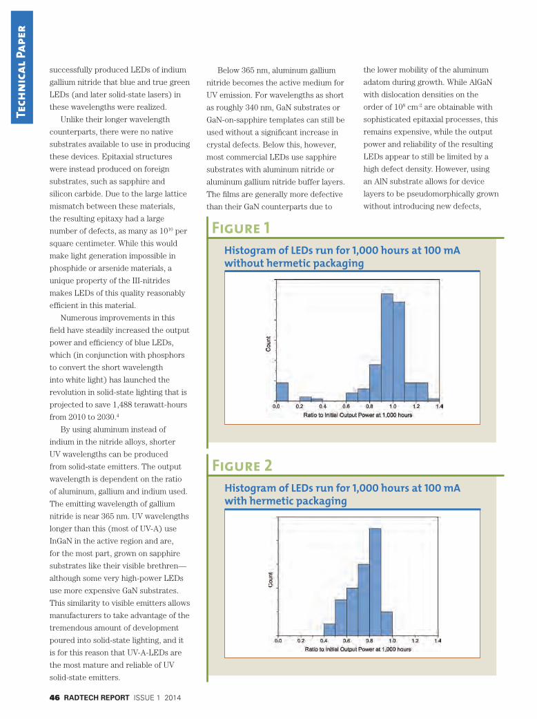
Figure 1Histogram of LEDs run for 1,000 hours at 100 mA without hermetic packaging
Figure 2Histogram of LEDs run for 1,000 hours at 100 mA with hermetic packaging

ISSUE 1 2014 RADTECH REPORT 47
Tech
nica
l Pap
er
producing LEDs with dislocation
counts less than 106 cm-2. It is for this
reason that the highest power, most
reliable devices in the mid-UV will
come from AlN substrate technology.
The shortest wavelength III-nitride
LED produced consisted almost
entirely of aluminum nitride and
emitted at 210 nm.5 This, however,
was only a proof of concept and
emitted very little light. Currently,
the nature of the dopants used to
produce carriers in AlN and AlGaN
is such that the wavelength limit of
commercializable UV-LEDs is around
235 nm.6 In general, the efficiency
of an LED decreases as one moves
deeper into the UV. Some of this is due
to the material challenges of working
with aluminum gallium nitride, as the
dopant species that provide carriers
requires more energy to activate.
However, the lack of research funding
into the mid-UV is also a contributing
cause. When the Defense Advanced
Research Projects Agency funded a
two-year program to increase power
output and efficiency in wavelengths
below 280 nm, a large improvement
was achieved in the targeted
wavelengths, pushing external
quantum efficiencies to more than 5%.
The ideal emission wavelengths for
LEDs produced on AlN templates and
substrates range from 250 to 290 nm.
Below these wavelengths, significant
research is needed to mitigate the
low electrical conductivity of high
aluminum composition AlGaN, and
low quantum efficiency of the devices.
Above about 300 nm, the lattice
mismatch between the corresponding
AlGaN layers and the underlying
aluminum nitride makes it difficult to
produce epitaxial structures without
introducing an increased number of
crystal lattice dislocations.
Crystal IS has successfully produced
low-defect density AlN substrates for
mid-UV-LEDs. The optoelectronic
AlGaN structures epitaxially grown
on these are pseudomorphically
strained to the substrate, producing
no additional defects through the
active region. This defect reduction
both improves the wall-plug efficiency
of the LEDs and reduces the heat
generated in the chip, which, in turn,
reduces the output power degradation
both in the short term as the device
achieves thermal equilibrium and the
longer term. UV-C-LEDs grown on
AlN substrates show a lower thermal
derating than even UV-A-LEDs on
sapphire substrates, while a test of
170 UV-C-LEDs fabricated over the
course of six months showed a median
degradation of less than 4% after 1,000
hours of continuous operation at 100
mA. Hermetically sealing the LED in
a TO-39 package further eliminated
catastrophic failures. (Figures 1 and 2)
Figure 3Light output versus input current for 268 nm Crystal IS LEDs tested by the U.S. Army Research Laboratory7
Figure 4Efficiency versus input current for 268 nm Crystal IS LEDs tested by the U.S. Army Research Laboratory7

48 RADTECH REPORT ISSUE 1 2014
Tech
nica
l Pap
er
A key efficiency limitation in
UV-LEDs is managing the light output
—both in extracting the light from
the AlGaN layers from which it is
generated and directing the light to the
desired surface in a uniform manner.
Many light extraction techniques have
been developed for visible LEDs to
use in solid-state lighting applications.
These are both more difficult and more
Figure 5Light output versus input current for 278 nm Crystal IS LEDs tested by the U.S. Army Research Laboratory7
Figure 6Efficiency versus input current for 278 nm Crystal IS LEDs tested by the U.S. Army Research Laboratory7
critical to use with UV-LEDs as the
index of refraction difference between
the III-nitride material and the air
increases with increasing bandgap,
resulting in greater internal reflection
at the interface and less light
extraction. Crystal IS has increased
the extraction efficiency of our LEDs
from 2.5% on-wafer to 15% through
thinning the AlN substrate after
fabrication and the use of a
UV-transparent encapsulant.
These extraction improvements
coupled with improvements in the
epitaxial structure of the device has
allowed Crystal IS to achieve high
output powers from a single LED on an
820 µm by 820 µm chip with an active
area of 0.37 mm2. Figures 3-6 show the
light output versus current for devices
emitting at 268 and 278 nm
under both continuous and pulsed
operation as measured by the U.S.
Army Research Laboratory. The two
current input methods diverge only
slightly beginning above 150 mA as
device self-heating begins to limit
the output power of the continuously
driven LED. This shows in the external
quantum efficiency (the ratio of the
extracted photons to the injected
carriers) and wall-plug efficiency
(the ratio of the optical power emitted
to the input electrical power) where
the efficiency loss due to heating is
between 9 and 15%.
Note that the conditions for pulsed
operation (40 µs pulses and a 0.4%
duty cycle) result in the device being
turned on and off 100 times a second.
This is only possible due to the
solid-state nature of the LED and its
instant turn-on. LEDs have been run
in this mode for thousands of hours
with no increase in degradation over
continuously driven devices. This
greatly extends the lifetime in a real-
world usage scenario, where the LED
needs to only be in operation when the
application calls for it, as opposed to
the long warm-up times of traditional
UV lamps.
The final challenge is to evenly
distribute the generated UV light
across the desired area. As the
primary application looks to be water
purification, this distribution becomes
extremely important to avoid dead
spots where untreated water might slip
through. Crystal IS has done significant
ISSUE 1 2014 RADTECH REPORT 49
Tech
nica
l Pap
er
problems in longer UV wavelengths
leads us to believe that UV-C-LED
performance will exceed that of UV-B
for the near future. w
AcknowledgementsThis work was partially supported
by the New York State Energy
Research and Development Authority
(NYSERDA).
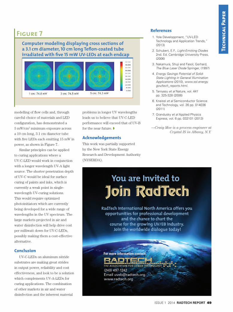
modelling of flow cells and, through
careful choice of materials and LED
configuration, has demonstrated a
5 mW/cm2 minimum exposure across
a 10 cm long, 3.1 cm diameter tube
with five LEDs each emitting 15 mW in
power, as shown in Figure 7.
Similar principles can be applied
to curing applications where a
UV-C-LED would work in conjunction
with a longer wavelength UV-A light
source. The shorter penetration depth
of UV-C would be ideal for surface
curing of paints and inks, which is
currently a weak point in single-
wavelength UV-curing solutions.
This would require optimized
photoinitiators which are currently
being developed for a wide range of
wavelengths in the UV spectrum. The
large markets projected in air and
water disinfection will help drive cost
per milliwatt down for UV-C-LEDs,
possibly making them a cost-effective
alternative.
ConclusionUV-C-LEDs on aluminum nitride
substrates are making great strides
in output power, reliability and cost
effectiveness, and look to be a solution
which complements UV-A-LEDs for
curing applications. The combination
of other markets in air and water
disinfection and the inherent material
Figure 7Computer modeling displaying cross sections of a 3.1 cm diameter, 10 cm long Teflon-coated tube irradiated with five 15 mW UV-LEDs at each endcap
References 1. Yole Développment, “UV-LED
Technology and Application Trends,” (2013)
2. Schubert, E.F., Light-Emitting Diodes 2nd. Ed. Cambridge University Press, (2006)
3. Nakamura, Shuji and Fasol, Gerhard, The Blue Laser Diode Springer, (1997)
4. Energy Savings Potential of Solid-State Lighting in General Illumination Applications (2010), www.ssl.energy.gov/tech_reports.html.
5. Taniyasu et al Nature, vol. 441 pp. 325-328 (2006)
6. Kneissl et al Semiconductor Science and Technology, vol. 26 pp. 014036 (2011)
7. Grandusky et al Applied Physics Express, vol. 6 pp. 032101 (2013)
—Craig Moe is a process engineer at Crystal IS in Albany, N.Y.