Embed Size (px)
Citation preview
UV Baked/Cured Photoresist Used as a Sacrificial Layer in
MEMS Fabrications
by Thomas P. Takacs, Jeff Pulskamp, and Ronald Polcawich
ARL-MR-602 February 2005 Approved for public release; distribution unlimited.
NOTICES
Disclaimers The findings in this report are not to be construed as an official Department of the Army position unless so designated by other authorized documents. Citation of manufacturer’s or trade names does not constitute an official endorsement or approval of the use thereof. Destroy this report when it is no longer needed. Do not return it to the originator.
Army Research Laboratory Adelphi, MD 20783-1197
ARL-MR-602 February 2005 UV Baked/Cured Photoresist Used as a Sacrificial Layer in
MEMS Fabrication
Thomas P. Takacs, Jeff Pulskamp, and Ronald Polcawich Sensors and Electron Devices Directorate, ARL
Approved for public release; distribution unlimited.
ii
REPORT DOCUMENTATION PAGE Form Approved OMB No. 0704-0188
Public reporting burden for this collection of information is estimated to average 1 hour per response, including the time for reviewing instructions, searching existing data sources, gathering and maintaining the data needed, and completing and reviewing the collection information. Send comments regarding this burden estimate or any other aspect of this collection of information, including suggestions for reducing the burden, to Department of Defense, Washington Headquarters Services, Directorate for Information Operations and Reports (0704-0188), 1215 Jefferson Davis Highway, Suite 1204, Arlington, VA 22202-4302. Respondents should be aware that notwithstanding any other provision of law, no person shall be subject to any penalty for failing to comply with a collection of information if it does not display a currently valid OMB control number. PLEASE DO NOT RETURN YOUR FORM TO THE ABOVE ADDRESS.
1. REPORT DATE (DD-MM-YYYY)
February 2005 2. REPORT TYPE
Final 3. DATES COVERED (From - To)
July to September 2003 5a. CONTRACT NUMBER
5b. GRANT NUMBER
4. TITLE AND SUBTITLE
UV Baked/Cured Photoresist Used as a Sacrificial Layer in MEMS Fabrication
5c. PROGRAM ELEMENT NUMBER
5d. PROJECT NUMBER
5e. TASK NUMBER
6. AUTHOR(S)
Thomas P. Takacs, Jeff Pulskamp, and Ronald Polcawich
5f. WORK UNIT NUMBER
7. PERFORMING ORGANIZATION NAME(S) AND ADDRESS(ES)
U.S. Army Research Laboratory ATTN: AMSRD-ARL-SE-SG 2800 Powder Mill Road Adelphi, MD 20783-1197
8. PERFORMING ORGANIZATION REPORT NUMBER ARL-MR-602
10. SPONSOR/MONITOR'S ACRONYM(S) 9. SPONSORING/MONITORING AGENCY NAME(S) AND ADDRESS(ES)
U.S. Army Research Laboratory 2800 Powder Mill Road Adelphi, MD 20783-1197
11. SPONSOR/MONITOR'S REPORT NUMBER(S)
12. DISTRIBUTION/AVAILABILITY STATEMENT
Approved for public release; distribution unlimited.
13. SUPPLEMENTARY NOTES 14. ABSTRACT
MEMS fabrication requires the release of compliant mechanical structures. A sacrificial layer is typically used to provide as a structural layer on which device layers can be deposited and subsequently removed to leave a suspended or freestanding device. There are several sacrificial layers commonly used in MEMS fabrication such as SiO2, polysilicon and polyimide. We have developed a sacrificial layer technique that can be used when many other sacrificial layers cannot be used. The use of photoresist that is Ultra Violet (UV) baked/cured as a sacrificial layer can save process steps, time and money. It can also be removed without the inherent problem of residues or stiction from wet processing, material by-products or the problematic issue of determining if the film has been completely removed.
15. SUBJECT TERMS
MEMS fabrication, UV photoresist
16. SECURITY CLASSIFICATION OF: 19a. NAME OF RESPONSIBLE PERSON Thomas P. Takacs
a. REPORT
Unclassified b. ABSTRACT
Unclassified c. THIS PAGE
Unclassified
17. LIMITATIONOF ABSTRACT
UL
18. NUMBEROF PAGES
14 19b. TELEPHONE NUMBER (Include area code) 301-394-2864
Standard Form 298 (Rev. 8/98) Prescribed by ANSI Std. Z39.18
iii
Contents
List of Figures iv
Acknowledgment v
Summary 4
References 5
Distribution List 6
iv
List of Figures
Figure 1. Novolak resin reaction mechanics...................................................................................2 Figure 2. UV cure recipe profile. ....................................................................................................2 Figure 3. Patterned softbaked photoresist over UV cured photoresist............................................3 Figure 4. UV Cured photoresist is intact after Au deposition and liftoff of soft baked
photoresist. .................................................................................................................................3

v
Acknowledgment
We would like to thank Joel L. Martin of General Technical Service for independent verification of this process.
vi
INTENTIONALLY LEFT BLANK
1
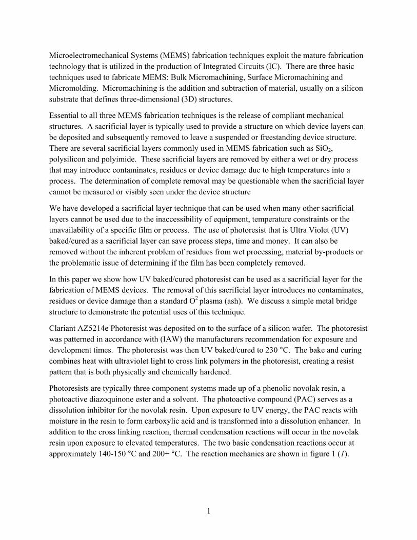
Microelectromechanical Systems (MEMS) fabrication techniques exploit the mature fabrication technology that is utilized in the production of Integrated Circuits (IC). There are three basic techniques used to fabricate MEMS: Bulk Micromachining, Surface Micromachining and Micromolding. Micromachining is the addition and subtraction of material, usually on a silicon substrate that defines three-dimensional (3D) structures.
Essential to all three MEMS fabrication techniques is the release of compliant mechanical structures. A sacrificial layer is typically used to provide a structure on which device layers can be deposited and subsequently removed to leave a suspended or freestanding device structure. There are several sacrificial layers commonly used in MEMS fabrication such as SiO2, polysilicon and polyimide. These sacrificial layers are removed by either a wet or dry process that may introduce contaminates, residues or device damage due to high temperatures into a process. The determination of complete removal may be questionable when the sacrificial layer cannot be measured or visibly seen under the device structure
We have developed a sacrificial layer technique that can be used when many other sacrificial layers cannot be used due to the inaccessibility of equipment, temperature constraints or the unavailability of a specific film or process. The use of photoresist that is Ultra Violet (UV) baked/cured as a sacrificial layer can save process steps, time and money. It can also be removed without the inherent problem of residues from wet processing, material by-products or the problematic issue of determining if the film has been completely removed.
In this paper we show how UV baked/cured photoresist can be used as a sacrificial layer for the fabrication of MEMS devices. The removal of this sacrificial layer introduces no contaminates, residues or device damage than a standard O2 plasma (ash). We discuss a simple metal bridge structure to demonstrate the potential uses of this technique.
Clariant AZ5214e Photoresist was deposited on to the surface of a silicon wafer. The photoresist was patterned in accordance with (IAW) the manufacturers recommendation for exposure and development times. The photoresist was then UV baked/cured to 230 °C. The bake and curing combines heat with ultraviolet light to cross link polymers in the photoresist, creating a resist pattern that is both physically and chemically hardened.
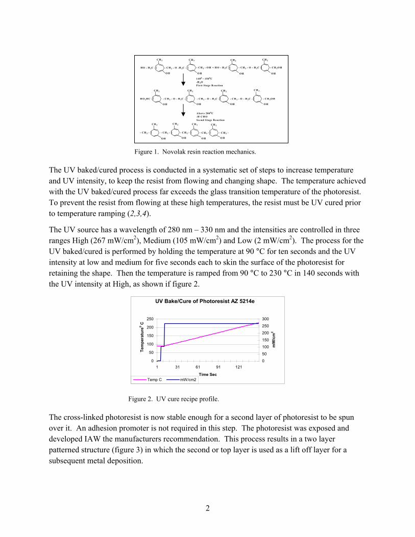
Photoresists are typically three component systems made up of a phenolic novolak resin, a photoactive diazoquinone ester and a solvent. The photoactive compound (PAC) serves as a dissolution inhibitor for the novolak resin. Upon exposure to UV energy, the PAC reacts with moisture in the resin to form carboxylic acid and is transformed into a dissolution enhancer. In addition to the cross linking reaction, thermal condensation reactions will occur in the novolak resin upon exposure to elevated temperatures. The two basic condensation reactions occur at approximately 140-150 °C and 200+ °C. The reaction mechanics are shown in figure 1 (1).
2
Figure 1. Novolak resin reaction mechanics.
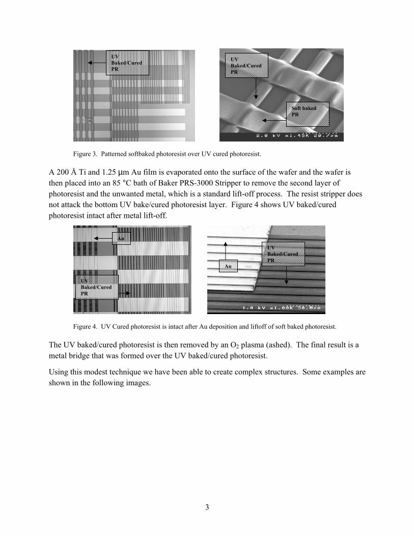
The UV baked/cured process is conducted in a systematic set of steps to increase temperature and UV intensity, to keep the resist from flowing and changing shape. The temperature achieved with the UV baked/cured process far exceeds the glass transition temperature of the photoresist. To prevent the resist from flowing at these high temperatures, the resist must be UV cured prior to temperature ramping (2,3,4).
The UV source has a wavelength of 280 nm – 330 nm and the intensities are controlled in three ranges High (267 mW/cm2), Medium (105 mW/cm2) and Low (2 mW/cm2). The process for the UV baked/cured is performed by holding the temperature at 90 °C for ten seconds and the UV intensity at low and medium for five seconds each to skin the surface of the photoresist for retaining the shape. Then the temperature is ramped from 90 °C to 230 °C in 140 seconds with the UV intensity at High, as shown if figure 2.
UV Bake/Cure of Photoresist AZ 5214e
0
50
100
150
200
250
1 31 61 91 121
Time Sec
Tem
pera
ture
0 C
0
50
100
150
200
250
300
mW
/cm
2
Temp C mW/cm2
Figure 2. UV cure recipe profile.
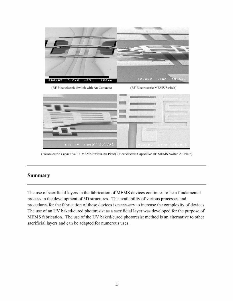
The cross-linked photoresist is now stable enough for a second layer of photoresist to be spun over it. An adhesion promoter is not required in this step. The photoresist was exposed and developed IAW the manufacturers recommendation. This process results in a two layer patterned structure (figure 3) in which the second or top layer is used as a lift off layer for a subsequent metal deposition.
H O - H 2C - - C H 2 - O -H 2C - - C H 2 - O H + H O - H 2C - - C H 2 - O - H 2C - - C H 2O H
C H 2 C H 2 C H 2 C H 2
O H O HO H O H
H O 2H C - - C H 2 - O - H 2C - - C H 2 - O - H 2C - - C H 2 - O - H 2C - - C H 2O H
C H 2 C H 2 C H 2 C H 2
O H O H O H O H
- C H 2 - - C H 2 -- C H 2 - - C H 2 - - C H 2 -
O H O H O H O H
C H 2 C H 2 C H 2C H 2
1400 - 1500C-H 2OF irst Stage R eaction
A bove 2000C-H C H OSecnd Stage R eaction
3
Figure 3. Patterned softbaked photoresist over UV cured photoresist.
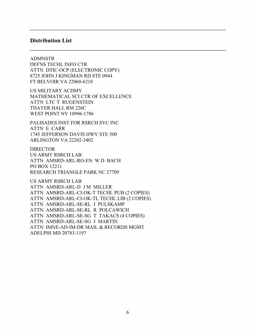
A 200 Å Ti and 1.25 µm Au film is evaporated onto the surface of the wafer and the wafer is then placed into an 85 °C bath of Baker PRS-3000 Stripper to remove the second layer of photoresist and the unwanted metal, which is a standard lift-off process. The resist stripper does not attack the bottom UV bake/cured photoresist layer. Figure 4 shows UV baked/cured photoresist intact after metal lift-off.
Figure 4. UV Cured photoresist is intact after Au deposition and liftoff of soft baked photoresist.
The UV baked/cured photoresist is then removed by an O2 plasma (ashed). The final result is a metal bridge that was formed over the UV baked/cured photoresist.
Using this modest technique we have been able to create complex structures. Some examples are shown in the following images.
UV Baked/Cured PR
UV Baked/Cured PR
UV Baked/Cured PR
Au
UV Baked/Cured PR
Au
Soft baked PR
4
(RF Piezoelectric Switch with Au Contacts) (RF Electrostatic MEMS Switch)
(Piezoelectric Capacitive RF MEMS Switch Au Plate) (Piezoelectric Capacitive RF MEMS Switch Au Plate)
Summary
The use of sacrificial layers in the fabrication of MEMS devices continues to be a fundamental process in the development of 3D structures. The availability of various processes and procedures for the fabrication of these devices is necessary to increase the complexity of devices. The use of an UV baked/cured photoresist as a sacrificial layer was developed for the purpose of MEMS fabrication. The use of the UV baked/cured photoresist method is an alternative to other sacrificial layers and can be adapted for numerous uses.

5
References
1. Orvek, K. J.; Seha, T.; Hemmings S.; Clark, D. Deep UV and Thermal Hardening of Novolak Resists. SPIE/Advances in Resist Technology and Processing IV 1987. Santa Clara. CA, 771, 281–288.
2. Spiertz, E. J.; Vollenbroek, F. A.; Verhaar R. D.; Dil, J. G. UV Hardening of Novolak Resist Patterens. Mircrocircuit Engineering 84 Proceedings, Berlin. 1984
3. Allen, R.; Forster, M.; Yen, Y. T. Deep U.V. Hardening of Positive Photoresist Patterns. J. Electrochemical Soc. 1982, 129, 1380.
4. DeForest, W. S. Photoresist Materials and Processes; McGraw-Hill, N.Y., 1975, 47–60.
6
Distribution List
ADMNSTR DEFNS TECHL INFO CTR ATTN DTIC-OCP (ELECTRONIC COPY) 8725 JOHN J KINGMAN RD STE 0944 FT BELVOIR VA 22060-6218
US MILITARY ACDMY MATHEMATICAL SCI CTR OF EXCELLENCE ATTN LTC T RUGENSTEIN THAYER HALL RM 226C WEST POINT NY 10996-1786
PALISADES INST FOR RSRCH SVC INC ATTN E CARR 1745 JEFFERSON DAVIS HWY STE 500 ARLINGTON VA 22202-3402
DIRECTOR US ARMY RSRCH LAB ATTN AMSRD-ARL-RO-EN W D BACH PO BOX 12211 RESEARCH TRIANGLE PARK NC 27709
US ARMY RSRCH LAB ATTN AMSRD-ARL-D J M MILLER ATTN AMSRD-ARL-CI-OK-T TECHL PUB (2 COPIES) ATTN AMSRD-ARL-CI-OK-TL TECHL LIB (2 COPIES) ATTN AMSRD-ARL-SE-RL J PULSKAMP ATTN AMSRD-ARL-SE-RL R POLCAWICH ATTN AMSRD-ARL-SE-SG T TAKACS (4 COPIES) ATTN AMSRD-ARL-SE-SG J MARTIN ATTN IMNE-AD-IM-DR MAIL & RECORDS MGMT ADELPHI MD 20783-1197


![Phase-out AZ5214E EU version - MicroChemicals€¦ · AZ 5214E [EU] AZ 5214E [JP] Substrate 6'' bare silicon (HMDS prime) Photoresist name AZ 5214E [EU] AZ 5214E [JP] Film thickness](https://img.pdfslide.us/doc/110x75/61281ef342dcfe3f5c0494c0/phase-out-az5214e-eu-version-microchemicals-az-5214e-eu-az-5214e-jp-substrate.jpg)