Embed Size (px)
Citation preview

ARCHIVES OF ELECTRICAL ENGINEERING VOL. 67(2), pp. 447–460 (2018)
DOI 10.24425/119652
Using the real-time simulator for prototypingpower electronics inverter
MARCIN BASZYNSKI1, MARCIN SZLOSEK2
1 AGH University of Science and Technologyal. Mickiewicza 30, 30-059 Kraków, Poland
e-mail: [email protected]
2 ABB Corporate Research Center31-038 Krakow, ul. Starowislna 13A, Poland
e-mail: [email protected]
(Received: 27.09.2017, revised: 15.04.2018)
Abstract: This paper deals with real-time (RT) simulators applied in power electronicapplications and implemented in a real inverter. The process of preparing and starting upan active rectifier prototype (with an active filter function), using the real-time OPAL RTsimulator is given. The control system of the converter and the results of simulation usingthe Matlab/Simulink suite are discussed.
Key words: numerical simulation, rectifiers, active filters, Real time systems
1. Introduction
The advancements of high computing power digital control systems have made it possible toconstruct increasingly complex topologies of power electronics systems [1, 2]. The complexityof the control systems for modern topologies have resulted in various advancements made tosimulation tools. Computer programs for analyzing systems in limited time windows (e.g. Mat-lab/Spice) make it possible to become initially acquainted with the principle of operation of adevice and allow a regulation system diagram to be prepared [1–5]. The usability of these pro-grams in the process of prototype start-up is limited. Real-time simulators (RTS) are very usefulduring prototyping [6–10]. Such simulators are equipped with a set of analog and digital outputsand inputs. The analog outputs of the simulator are connected to the measurement channels ofa real control system (prototype). The digital outputs controlling e.g. the converter transistorsare connected to the digital inputs of the simulator. In such a configuration, the power circuit(converter with passive elements and supply network or motor) is modeled in the simulator. Thiskind of simulation is called Hardware in the Loop (HIL) [8, 9, 11, 12].

448 M. Baszynski, M. Szlosek Arch. Elect. Eng.
HIL simulations are very useful at the initial stage of developing a prototype of a controlsystem for power electronics converters operating with a power supply network of high short-circuit power. The HIL simulation makes it possible to verify control algorithms in conditionsvery close to reality with a reduced risk of damage of any elements due to incorrect controlimplementation. During testing in real conditions (without HIL), algorithmic errors may causedamage of power electronics systems [4, 6, 7, 9, 12]. Moreover, these errors are usually difficultto detect because of the distorted operation of debugging probes and the destruction of the powerelectronics elements.
An incorrect transistor control sequence causes high and fast-changing current to flow, re-sulting in interference in the operation of debugging probes or even damage to power electronicselements. The HIL simulation is resistant to these hazards because no high-value currents everflow in the system, no high voltages appear (no problem with interferences), and there is no riskof damaging any of the converter power circuit elements. Fig. 1 presents successive stages ofdevelopment of an operating power electronics converter.
Fig. 1. Stages of work on constructing a power electronics
At the beginning of the control system development, simulations are performed in tools likeSpice or Matlab. Simulations [1–5] of this type make it possible to get acquainted with a newtopology, to develop a control system, and to check the system performance in dynamic states.After finishing the simulations and getting familiar with the properties of the tested converter,one may proceed to the implementation of the protection and regulation system in the targetcontroller based on a digital chip (DSP/FPGA). Then the correctness of the operation of theprepared controller is verified with the use of a real-time simulator (RTS), which substitutesthe real grid and switching elements of the converter (IGBT/MOSFET) together with passiveelements. The converter transistors are controlled by the controller on the basis of voltage andcurrent measurements calculated by the RTS. The entire control channel is verified in near-realconditions: A/D converters, a regulation system, modulator. This makes it possible to detectmost errors made during coding without placing the system at risk of damage. After completionof the HIL simulations, one may safely proceed to testing the system in real conditions (with aconnection to the power supply network).
The paper will present the process of constructing a converter using a real-time simulatorOpalRT OP5600 with the example of a three-phase active rectifier.
2. Principle of operation of the rectifier
The control system of the voltage-raising three-phase active rectifier with grid line currentshaping is realized in a rotating dq frame. In this reference system, sinusoidal signals of thesynchronous frequency are represented as constant values, which enables the use of well-known
Vol. 67 (2018) Using the real-time simulator for prototyping power electronics inverter 449
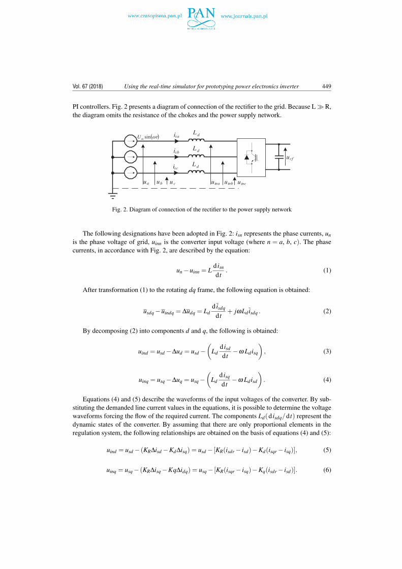
PI controllers. Fig. 2 presents a diagram of connection of the rectifier to the grid. Because L ≫ R,the diagram omits the resistance of the chokes and the power supply network.
( )tUm ωsindisa
L
disbL
discL
uinb u incuinau b u cua
ucf
Fig. 2. Diagram of connection of the rectifier to the power supply network
The following designations have been adopted in Fig. 2: isn represents the phase currents, unis the phase voltage of grid, uinn is the converter input voltage (where n = a, b, c). The phasecurrents, in accordance with Fig. 2, are described by the equation:
un −uinn = Ld isn
d t. (1)
After transformation (1) to the rotating dq frame, the following equation is obtained:
usdq −uindq = ∆udq = Ldd isdq
d t+ jωLd isdq . (2)
By decomposing (2) into components d and q, the following is obtained:
uind = usd −∆ud = usd −(
Ldd isd
d t−ω Ld isq
), (3)
uinq = usq −∆uq = usq −(
Ldd isq
d t−ω Ld isd
). (4)
Equations (4) and (5) describe the waveforms of the input voltages of the converter. By sub-stituting the demanded line current values in the equations, it is possible to determine the voltagewaveforms forcing the flow of the required current. The components Ld(d isdq/d t) represent thedynamic states of the converter. By assuming that there are only proportional elements in theregulation system, the following relationships are obtained on the basis of equations (4) and (5):
uind = usd − (KR∆isd −Kd∆isq) = usd − [KR(isdr − isd)−Kd(isqr − isq)], (5)
uinq = usq − (KR∆isq −Kq∆idq) = usq − [KR(isqr − isq)−Kq(isdr − isd)]. (6)
450 M. Baszynski, M. Szlosek Arch. Elect. Eng.
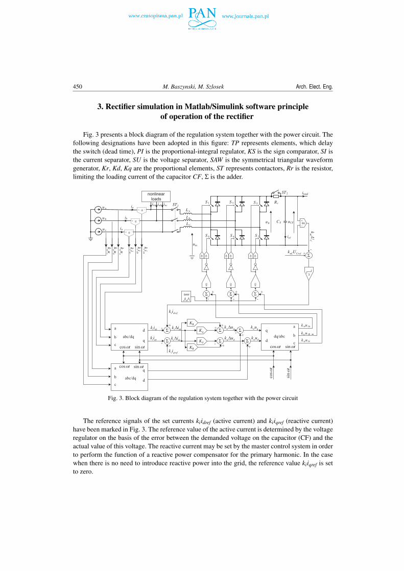
3. Rectifier simulation in Matlab/Simulink software principleof operation of the rectifier
Fig. 3 presents a block diagram of the regulation system together with the power circuit. Thefollowing designations have been adopted in this figure: TP represents elements, which delaythe switch (dead time), PI is the proportional-integral regulator, KS is the sign comparator, SI isthe current separator, SU is the voltage separator, SAW is the symmetrical triangular waveformgenerator, Kr, Kd, Kq are the proportional elements, ST represents contactors, Rr is the resistor,limiting the loading current of the capacitor CF, Σ is the adder.
-
-to-
TP
TP
TP
TP
TP
TP
SI
+ -
SI
+ -
SU
+
-
PI
SAW
KS
KS
KS
SI
+ -
Σ
tωcos tωsin
abc/dq
a
b
c
d
q
tωcos tωsin
dq/abc
a
b
c
q
d
KR
Kd
Kq
KR
Σ
Σ
tωcos tωsin
abc/dq
a
b
c
q
d
Σ
Σ
Σ
Σ
+
+
-
-
dsiik
qsiik
dsi ik Δ
dsi ik Δ
++
-+
qu uk Δ
du uk Δ+
-
+-
quuk
duuk
drefiik
qrefiik
tω
cos
tω
sin
u ra
u rb
u rc
k u
ku
ku
Σ Σ
Σ
ST2
R r
au uk
bu uk
cu uk
+ + +
- - -
+-
CF uCF
CrefuCUk
CuC U
k
u a
u b
u c
L a
L b
L c
S 1 S 3 S 5
S 4 S 6 S 2
ud
iload
icf
uin
ST1
sci ik
sbi ik
sai ik
nonlinear
loads
ina inb incia
ib
ia
Fig. 3. Block diagram of the regulation system together with the power circuit
The reference signals of the set currents kiidref (active current) and kiiqref (reactive current)have been marked in Fig. 3. The reference value of the active current is determined by the voltageregulator on the basis of the error between the demanded voltage on the capacitor (CF) and theactual value of this voltage. The reactive current may be set by the master control system in orderto perform the function of a reactive power compensator for the primary harmonic. In the casewhen there is no need to introduce reactive power into the grid, the reference value kiiqref is setto zero.

Vol. 67 (2018) Using the real-time simulator for prototyping power electronics inverter 451
Since the control system aims to keep the sinusoidal current waveforms in the grid in phasewith the voltage, it can also be used as an active filter (when the reactive power compensationis not being performed). In such a case a nonlinear receiver is connected between the currentseparators (SI) and the mains chokes (La, Lb, Lc).
The correctness of the control concept (Fig. 3), the dynamic states of operation of the con-verter (step switching on the load in the DC circuit), and the ability of the system to perform thefunction of an active filter have been verified in the simulation (Matlab/Simulink software).
In the simulation it has been assumed that the system is being supplied from a three-phasenetwork of line-to-line voltage equal to 127 V, the maximum converter current is equal to 15 A,and the set voltage of capacitor is equal to 420 V. Fig. 4 presents the waveforms of currents andvoltages characterizing the operation of the rectifier.
0 0.02 0.04 0.06 0.08 0.1 0.12 0.14 0.16300
320
340
360
380
400
420
440uCF
t1
t2
t3
t4
0
0
20A
80V ua
ia
ina
Fig. 4. Waveforms of power supply line phase volt-age (ua), power supply line current (ia), nonlinearreceiver current (ina), and DC link voltage (uCF ).Results of simulation in Matlab/Simulink software;t1 – charging capacitor CF, t2 – idle state, t3 – loadconnected to DC-link, t4 – load connected to DC-link and nonlinear load working, t5 – nonlinear loadworking and transferring energy from DC-link to
the grid
300
320
340
360
380
400
420
440
0 0.02 0.04 0.06 0.08 0.1 0.12 0.14 0.16
uCFt1
t2
t3
t4
t5
0
10A
80Vua
iaina
Fig. 5. Oscilloscope traces depicting the possibilityof introducing reactive power into the power supplyline by the converter t1 – charging capacitor CF, t2 –idle state, t3 – load connected to DC-link, t4 – loadconnected to DC-link, nonlinear load working andgenerating the inductive reactive power, t5 – loadconnected to DC-link, nonlinear load working and
generating the capacitive reactive power
Fig. 4 presents the waveforms of grid phase voltage (ua), grid current (ia), nonlinear receivercurrents (ina), and DC- link voltage (uCF). Four characteristic spans of the system operationhave also been marked: t1: capacitor charging from the value equal to the line-to-line voltageamplitude to the set voltage (420 V), t2: after this time the DC receiver connected to the capacitoris switched on, t3: the nonlinear receiver is switched on (in this case, a three-phase diode rectifierwith resistive load), t4: the capacitor voltage rises above the set voltage. Fig. 4 does not showthe initial charging of the capacitor from the voltage equal to zero to the amplitude of the gridvoltage, because charging is then performed by the diode rectifier (the antiparallel diodes of thebridge transistors). Switching of the transistors does not affect the shape of the power supply linecurrent at that time, the value of the current at that time is limited by the resistor (Rr). In the timespan t1 the current is already sinusoidal and in phase with the voltage, the value of the currentis limited by the limit (15 A) set by the voltage regulator (of PI structure). After the capacitoris charged to the set level, the line current decreases to the value resulting from the leakage of

452 M. Baszynski, M. Szlosek Arch. Elect. Eng.
the capacitor and the power losses of the converter. After the time t2 the receiver is connected tothe capacitor (in the case of the simulation it is a 75 Ω resistor). After the resistor is connected,the power supply line current is sinusoidal and in phase with the voltage, the capacitor voltagedecreases by approx. 1.5 V. This results from the adopted structure of the regulation system.After the time t3 the nonlinear receiver is switched on (the DC receiver connected to the capacitorremains switched on). After switching on the nonlinear receiver, the capacitor voltage decreasesby approx. 2.5 V. This change is small, it does not exceed 0.6% of the set voltage. Despite theappearance of nonlinear currents, the system has maintained the sinusoidal currents in the powersupply line in phase with the voltage. In the last analyzed time-span the capacitor voltage hasincreased above the set value (a braking motor, another energy source, e.g. PV, etc.). This resultsin the sign of the regulator voltage error being changed to negative, and as a consequence, theenergy from the capacitor starts to be transferred to the power supply line. As follows from thepresented analysis, the system described has been operating correctly in all cases and has fulfilledthe function of a rectifier and an active filter, making it possible to transfer the energy from thecapacitor to the grid (four-quadrant operation).
If the nonlinear receiver introduces reactive power into the grid line, the converter will com-pensate for it. In the presented example (Fig. 3), the nonlinear receiver is the three-phase dioderectifier loaded with the resistor. This type of nonlinear receiver used in the example is loadingthe mains with reactive power. As it results from the waveforms in Fig. 4, after switching onthe diode rectifier the grid current remains sinusoidal and in phase with the voltage, i.e. the ana-lyzed converter has correctly compensated the reactive power. The described system can fulfil anadditional function of introducing additional reactive power into the grid. This is performed ondemand of the master control system. Simulation traces depicting such operation are presented inFig. 5. The same functions as presented in Fig. 4 are realized in the time spans t1, t2, t3. After thetime t4 the converter introduces inductive reactive power into the mains. In the last period fromthe time t5 capacitive reactive power is being introduced into the grid. Generating the additionalreactive power by the converter does not disturb other functions of the system, i.e. stabilizing thecapacitor voltage and filtering the higher harmonics introduced by the nonlinear receiver.
4. Coding of the control system
A system for controlling a real active rectifier, based on an FPGA chip, has been preparedon the basis of the diagram given in Fig. 3 and the simulation performed in Matlab/Simulinksoftware. A picture of the controller is presented in Fig. 6. Presented rectifier is part of the highspeed flywheel energy storage system. In final solution the FPGA chip has controlled rectifierand flywheel inverter. To meet this requirement, the FPGA has been chosen instead of DSP.
The digital control and regulation circuit has been based on the FPGA matrix EP3C16E144from Cyclone III family manufactured by Altera/Intel. The eight-channel bipolar 12-bit A/Dconverter MAX1308 has been used for the measurement data acquisition. The applied converterallows fast conversion of analog data (conversion time of all channels To = 1.98 µs) and datatransfer to the FPGA chip with bus throughput of 456 ksps. In addition, the controller has beenequipped with: four galvanically separated general-purpose binary inputs, triple inputs accordingto the standard RS-422/RS-485 allowing the connection of e.g. a BLDC motor positioning system

Vol. 67 (2018) Using the real-time simulator for prototyping power electronics inverter 453
Fig. 6. A picture of the controller used for implementingthe control system from Fig. 2
or an encoder, six binary outputs of voltage 15 V or 5 V, nineteen binary outputs aimed fortransistor control. The controller board also comprises a microSD card socket, USB-OTG, andRJ45 socket allowing the system to be connected to the Internet.
A description of the control system structure has been prepared in the VHDL language (VeryHigh Speed Integrated Circuits Hardware Description Language), using the Quartus II suite (ver-sion 13.1 Web Edition). All computational operations are based on a fixed-point notation. In thesystem it has been assumed that voltages and currents are described using sixteen-bit vectors,where the currents are represented in Q10 format, and the voltages – in Q5 format. The calibra-tion block is responsible for adapting the data from A/D converters to the selected format. Suchapproach makes it possible to easily change the parameters during the transition from the HILsimulator to the real system. The algorithm for synchronization with the grid is operating on thebasis of the principle of ABC-DQ conversion and is described in detail in [13]. As it results fromthe description of the control system, in order to determine the control it is necessary to knowthe phase voltages (Equations (6) and (7)). However, in many cases it is not possible to performmeasurements of phase voltages, therefore line-to-line voltages are used for synchronization inthe described solution. After a correct synchronization, the system introduces a phase shift ofπ/6 into the synchronized waveform, so that it corresponds to the phase voltages.
5. HIL simulation
Simulation techniques became a very important tool in the development and analysis of com-plex dynamic systems in recent years. Due to a significant increase in the computational capa-bilities of modern computers, engineers are able to easily perform analyses of the performanceof the designed control systems in a short time. Thanks to the use of computer simulation, thecorrectness of a control algorithm can be verified without possessing a physical controller. Suchan approach allows a significant reduction of the product development time, as well as substantialsavings on costly physical prototypes.
The OP5600 simulator by OPAL-RT has been used during the work presented in this paper.The simulator is built on the basis of two six-core processors Intel Xeon Six-Core 3.33 GHz12 M Cache 6.4 GT/s and the FPGA chip Xilinx Spartan 3 used for signal processing, it has

454 M. Baszynski, M. Szlosek Arch. Elect. Eng.
16 analog input channels, and 64 each of digital outputs and inputs. The analog outputs boardOP5330 allows voltage signals in the range of +/−15 V to be generated with a sampling rate of1 MS/s (simultaneous sampling of all channels) and a resolution of 16 bits. The digital outputsboard OP5354 makes it possible to control 32 galvanically isolated channels, with simultaneoussampling up to 40 MS/s, with a high logic state voltage range of 5–30 V. The digital inputsboard OP5353 comprises 32 optically isolated channels, sampled simultaneously at a rate up to10 MS/s. The acceptable range of input voltages is 4–100 V.
Fig. 7. HIL simulator concept Fig. 8. Structure of the model with division into thecomputing subsystem and the console subsystem
The simulation model has been prepared in Matlab/Simulink software, using OPAL-RT andSimPowerSystemstoolboxes. It has been divided into the computing subsystem – comprisingthe SimPowerSystems model as well as I/O interfaces and saving the signals to a file, beingcalculated in the simulator, and the console model which is executed in the user computer andallows a non-line preview of the model state, as well as setting some input values (triggering thewaveform logging, control signals for breakers and switches). After model preparation using theRT-LAB environment, the code and executable files have been generated. The structure of themodel is presented in Fig. 8.
In the case of the real-time simulation a very important parameter to consider is the time stepof simulation. The shorter the time step, the more precise the simulation results; the longer thetime step, the more time for computation and the higher possible complexity of the model. Thechoice of adequate time step must be a result of careful analysis, and must take into account thecomputational complexity of the model and the switching frequency (the higher the switchingfrequency, the shorter the time step). The time step of simulation for the presented model hasbeen established at 15 µs. In the case of inadequate choice of the time step system may becomeunstable, give inadequate results, and some of the transistor control signals may be missed aswell (in the case of the modulation duty cycle near to 0 or 100%). An example of such situationis presented in Fig. 9. Fig. 9 presents the waveform of the phase voltage ua, the phase currentia, the PWM waveform generated by the controller (PWM1), and the PWM waveform read bythe OPAL simulator (PWM2). The computation step set in the simulator was too large, whichresulted in the control pulses not being correctly read. In the vicinity of the voltage crossingthe amplitude value, the duration time of the transistor triggering pulse was shorter than thecomputation step, therefore the simulator did not identify that pulse, and as a result, it wronglycalculated the grid current.

Vol. 67 (2018) Using the real-time simulator for prototyping power electronics inverter 455
Despite the performed testing of the control system using the tools of the Quartus II suite, nu-merical errors could be observed during initial starts of the controller with the OpalRT simulator,resulting in the flow of currents at the level of 1.5 kA and settling of the capacitor voltage at thelevel of 4.5 kV. After correcting the control program and removing the errors, tests of the controlsystem have been performed. First, the basic assumptions set for the converter have been verified:stabilization of the capacitor voltage, the sinusoidal grid current in phase with the voltage (thesystem did not compensate the reactive power). Oscilloscope traces confirming the fulfillment ofthe set requirements (waveforms recorded with step switching on the DC receiver connected tothe capacitor) are presented in Fig. 10.
Fig. 9. Example of inadequately chosen computa-tion step
Fig. 10. Waveforms of the phase voltage ua, powersupply line current ia, capacitor voltage uc f at step
switching on the DC receiver
After the receiver was connected, the capacitor voltage decreased by 0.5%, the grid currentwas sinusoidal and in phase with the voltage. Next, the operation of the converter as an activefilter and a reactive power compensator has been verified (Fig. 10). A three-phase diode rectifierwas connected with the DC receiver switched on.
In the case of a capacitor voltage increase above the set value, the tested system shouldreturn the energy from the capacitor to the grid. Oscilloscope traces recorded in such situationare presented in Fig. 11.
Fig. 11. Waveforms of the phase voltage ua, gridcurrent ia, DC-link voltage at a step increaseof the capacitor voltage forced by an external
event (e.g. motor braking)

456 M. Baszynski, M. Szlosek Arch. Elect. Eng.
It follows from the presented oscilloscope traces that the system was performing correctly.After the set voltage of the DC-link was exceeded, the phase of the grid current has changed, andthe inverter started to return energy to the mains.
Fig. 12 presents oscilloscope traces depicting the possibility of introducing a primary har-monic of reactive current of inductive character (Fig. 12a) and capacitive character (Fig. 12b)into the power supply line. The system receives the command to start to supply the reactivepower of specified value from the master supervision system (e.g. from a local transmissionsystem operator).
(a) (b)
Fig. 12. Waveforms of the phase voltage ua, power supply line current ia, capacitor voltage, phase shift φbetween the voltage and current of the power supply line at introducing: (a) inductive; (b) capacitive
Fig. 13 presents the oscilloscope trace recorded during termination of returning energy tothe power supply line at switched on DC- link receiver and filtering of higher harmonics of thenonlinear receiver.
Fig. 13. Waveforms of the phase voltage ua,power supply line current ia, nonlinear receivercurrent ina, capacitor voltage during termination
of returning energy to the power supply line
6. Experimental setup
After completion of work with the HIL simulator, the verified algorithm was transferred intoa real converter with a power circuit in accordance with the diagram from Fig. 3 and basedon IGBT modules SK25GD126ET manufactured by Semicron (maximum switching frequency

Vol. 67 (2018) Using the real-time simulator for prototyping power electronics inverter 457
equal 50 kHz). In the presented rectifier, switching frequency was equal 12 kHz. The frequencyassumed was much below the capabilities of the used transistors because it was adapted to easiertransition to a more powerful system using IPM modules. A system identical to the one usedfor realization of the HIL simulation (Fig. 6) has been applied as the control system. Since theanalog outputs of the OPAL-RT simulator accepted values in the range of ±15 V, whereas thereal measurement channels gave signals at the level of ±10 V, it was necessary to change thegains in the analog channels and the corresponding gains in the digital channel. These changes,together with verification of their correctness, required approx. 3 hours of work. Upon startingthe experimental system, and confirming that the control system was operating correctly, theprotection blocks were deactivated.
Since perfect sinusoidal waveforms of grid voltages had been assumed in Matlab/Simulinkand HIL simulation, it was necessary to correct the settings of the regulators so that the gridcurrent would be sinusoidal with deformed voltages. Use of deformed voltages in the HIL sim-ulation would result in increasing the complexity of computations performed by the simulator,thus increasing the computation step.
Fig. 14 presents an oscilloscope trace recorded during precharge of the DC link capacitor.After switching on the system, the transistors are blocked, the contactor ST2 (Fig. 2) remains
open, and the capacitor charging current flows through the diodes of the transistor bridge. Thevalue of the charging current is limited by the resistor Rr (time span t1 in Fig. 4). After chargingthe capacitor to the amplitude value of the line-to-line voltage, the contactor ST2 short-circuits,the resistor Rr, and the transistors start pulsing, causing the capacitor voltage to increase to theset value (time span t2 in Fig. 4). The value of the current within this time span is limited by theregulation system (the maximum value of the voltage regulator from Fig. 2).
Fig. 14. Waveforms of the voltage and current of thepower supply line during capacitor charging
Fig. 15. Waveforms of the phase voltage ua, powersupply line current ia, capacitor voltage uc f at step
switching on the DC receiver
Waveforms of the phase voltage ua, grid current ia, capacitor voltage uc f at step switching onthe DC receiver are presented in Fig. 15.
After the receiver was connected, the capacitor voltage decreased by 4.3%, and the gridcurrent remained sinusoidal and in phase with the voltage. Oscilloscope traces depicting theoperation of the rectifier as an active filter are presented in Fig. 16. A three-phase diode rectifierhas been connected to the grid.

458 M. Baszynski, M. Szlosek Arch. Elect. Eng.
Fig. 16. Waveforms of the phase voltage ua,power supply line current ia, nonlinear receivercurrent ina, capacitor voltage at switching on the
diode rectifier
Fig. 17 presents oscilloscope traces depicting the system operation at introducing a primaryharmonic of reactive current of inductive (Fig. 17a) and capacitive character (Fig. 17b) into thepower supply line.
(a) (b)
Fig. 17. Waveforms of the phase voltage ua, power supply line current ia, capacitor voltage, phase shiftφ between the voltage and current of the power supply line at introducing: (a) inductive; (b) capacitive
reactive power into the mains
Fig. 18 presents oscilloscope traces recorded during returning the DC link energy to the grid.
Fig. 18. Waveforms of the phase voltage ua,power supply line current ia, during returning
energy to the power supply line

Vol. 67 (2018) Using the real-time simulator for prototyping power electronics inverter 459
7. Summary
Because the ideal model of the grid has been used in the Matlab and HIL simulations (impe-dance is equal to zero, ideal sinusoidal voltage), it is difficult to make the quantitative compar-ison of these results with real measurements. In addition, in the HIL simulation the switchingfrequency was several times lower than in the test bed, therefore the results are not comparable.But comparing functionality (current shape, reactive power compensation, active filtration), theresults obtained from the test bed match the results obtained in Matlab/Simulink and HIL sim-ulation. This confirms the usability of these tools in prototyping of power electronics systems,especially in the case where the prototyped devices cooperate with a grid. The test of the controlsystem with the OPAL-RT simulator made it possible to safely verify the correctness of systemoperation in both static and dynamic states (initial choice of regulator parameters). Errors whichwould cause damage to semiconductor elements and would be difficult to diagnose in operationof a real system with a grid, even a low-power one, have been detected and removed during op-eration with the HIL simulator. By progressing through the simulation stages described in thepaper, the control system of the prototype has never reported exceeding the permissible value ofthe grid currents or the DC link capacitor voltage. Starting up the laboratory test bed requiredonly a few hours of work in order to scale the measurement channels.
References
[1] Wang C., Zhuang Y., Jiao J., Zhang H., Wang C., Cheng H., Topologies and Control Strategies ofCascaded Bridgeless Multilevel Rectifiers, IEEE Journal of Emerging and Selected Topics in PowerElectronics, vol. 5, no. 1, pp. 432–444 (2017).
[2] Pirog S., Baszynski M., Modelling a single phase multicell DC/AC inverter using FPGA, PrzegladElektrotechniczny, vol. 84, no. 2, pp. 84–87 (2008).
[3] Yaramasu V., Wu B., Rivera M., Rodriguez J., A New Power Conversion System for Megawatt PMSGWind Turbines Using Four-Level Converters and a Simple Control Scheme Based on Two-Step ModelPredictive Strategy—Part II: Simulation and Experimental, IEEE Journal of Emerging and SelectedTopics in Power Electronics, vo. 2, no. 1, pp. 14–25 (2014).
[4] Baszynski M., Power factor correction boost rectifiers for the household appliances, Przeglad Elek-trotechniczny, vol. 87, no. 3, pp. 237–242 (2011).
[5] Dagbagi M., Hemdani A., Idkhajine L., Naouar M.W., Monmasson E., Slama-Belkhodja I., ADC-Based Embedded Real-Time Simulator of a Power Converter Implemented in a Low-Cost FPGA:Application to a Fault-Tolerant Control of a Grid-Connected Voltage-Source Rectifier, IEEE Transac-tions on Industrial Electronics, vo. 63, no. 2, pp. 1179–1190 (2016).
[6] Stala R., Stawiarski L., Real-time models of PV arrays implemented in FPGAs, Przeglad Elektrotech-niczny, vol. 86, no. 2, pp. 358–363 (2010).
[7] Stala R., Penczek A., Mondzik A., Stawiarski L., A photovoltaic source I/U model suitable for hard-ware in the loop application, Archives of Electrical Engineering, vol. 66, no. 4, pp. 774–786 (2017).
[8] Hardy T., Jewell W., Hardware-in-the-Loop Wind Turbine Simulation Platform for a LaboratoryFeeder Model, IEEE Transactions on Sustainable Energy, vol. 5, no. 3, pp. 1003–1009 (2014).
[9] Hassanpoor A., Roostaei A., Norrga S., Lindgren M., Optimization-Based Cell Selection Method forGrid-Connected Modular Multilevel Converters, IEEE Transactions on Power Electronics, vol. 31,no. 4, pp. 2780–2790 (2016).

460 M. Baszynski, M. Szlosek Arch. Elect. Eng.
[10] Dargahi M., Ghosh A., Davari P., Ledwich G., Controlling current and voltage type interfacesin power-hardware-in-the-loop simulations, IET Power Electronics, vol. 7, no. 10, pp. 2618–2627(2014).
[11] Huerta F., Tello R.L., Prodanovic M., Real-Time Power-Hardware-in-the-Loop Implementationof Variable-Speed Wind Turbines, IEEE Transactions on Industrial Electronics, vol. 63, no. 3,pp. 1893–1904 (2017).
[12] Blaabjerg F., Teodorescu R., Liserre M., Timbus A.V., Overview of Control and Grid Synchronizationfor Distributed Power Generation Systems, IEEE Transactions on Industrial Electronics, vol. 53, no. 5,pp. 1398–1409 (2006).