Embed Size (px)
Citation preview
byTimm Meiwes
UserfriendlyWearable Networking forInteractive Fashion
Bachelor’s Thesissubmitted to theMedia Computing GroupProf. Dr. Jan BorchersComputer Science DepartmentRWTH Aachen University
Thesis advisor: Prof. Dr. Jan Borchers
Second examiner: Prof. Dr. Ulrik Schroeder
Registration date: 18.01.2019 Submission date: 18.05.2019


Eidesstattliche Versicherung
___________________________ ___________________________
Name, Vorname Matrikelnummer
Ich versichere hiermit an Eides Statt, dass ich die vorliegende Arbeit/Bachelorarbeit/ Masterarbeit* mit dem Titel
__________________________________________________________________________
__________________________________________________________________________
__________________________________________________________________________
selbständig und ohne unzulässige fremde Hilfe erbracht habe. Ich habe keine anderen als die angegebenen Quellen und Hilfsmittel benutzt. Für den Fall, dass die Arbeit zusätzlich auf einem Datenträger eingereicht wird, erkläre ich, dass die schriftliche und die elektronische Form vollständig übereinstimmen. Die Arbeit hat in gleicher oder ähnlicher Form noch keiner Prüfungsbehörde vorgelegen.
___________________________ ___________________________
Ort, Datum Unterschrift
*Nichtzutreffendes bitte streichen
Belehrung:
§ 156 StGB: Falsche Versicherung an Eides Statt
Wer vor einer zur Abnahme einer Versicherung an Eides Statt zuständigen Behörde eine solche Versicherung falsch abgibt oder unter Berufung auf eine solche Versicherung falsch aussagt, wird mit Freiheitsstrafe bis zu drei Jahren oder mit Geldstrafe bestraft.
§ 161 StGB: Fahrlässiger Falscheid; fahrlässige fals che Versicherung an Eides Statt
(1) Wenn eine der in den §§ 154 bis 156 bezeichneten Handlungen aus Fahrlässigkeit begangen worden ist, so tritt Freiheitsstrafe bis zu einem Jahr oder Geldstrafe ein.
(2) Straflosigkeit tritt ein, wenn der Täter die falsche Angabe rechtzeitig berichtigt. Die Vorschriften des § 158 Abs. 2 und 3 gelten entsprechend.
Die vorstehende Belehrung habe ich zur Kenntnis genommen:
___________________________ ___________________________
Ort, Datum Unterschrift

v
Contents
Abstract xiii
Uberblick xv
Acknowledgements xvii
Conventions xix
1 Introduction 1
2 Related work 3
2.1 Commercially available systems . . . . . . . 3
2.2 Academic systems . . . . . . . . . . . . . . . . 5
3 Own work 9
3.1 Requirements . . . . . . . . . . . . . . . . . . 9
3.1.1 I2C vs. Serial . . . . . . . . . . . . . . 10
3.2 Early Work . . . . . . . . . . . . . . . . . . . . 11
3.3 Board . . . . . . . . . . . . . . . . . . . . . . . 12
vi Contents
3.3.1 Upgrade . . . . . . . . . . . . . . . . . 13
3.3.2 Localisation . . . . . . . . . . . . . . . 14
3.3.3 Hardware . . . . . . . . . . . . . . . . 16
3.3.4 Software . . . . . . . . . . . . . . . . . 16
Mode Change . . . . . . . . . . . . . . 17
Communication . . . . . . . . . . . . . 18
Localisation Routine . . . . . . . . . . 19
3.4 Chips . . . . . . . . . . . . . . . . . . . . . . . 19
3.4.1 Simple Chips . . . . . . . . . . . . . . 21
Button . . . . . . . . . . . . . . . . . . 21
LED . . . . . . . . . . . . . . . . . . . . 22
Other . . . . . . . . . . . . . . . . . . . 22
3.4.2 I2C Chips . . . . . . . . . . . . . . . . 23
Seven-Segment-Display . . . . . . . . 23
Gyroscope . . . . . . . . . . . . . . . . 24
Display . . . . . . . . . . . . . . . . . . 26
Individually addressable LEDs . . . . 27
3.4.3 Challenges . . . . . . . . . . . . . . . . 28
4 Evaluation 31
4.1 User-friendliness . . . . . . . . . . . . . . . . 31
4.2 Wearability . . . . . . . . . . . . . . . . . . . . 33
Contents vii
4.3 Networking . . . . . . . . . . . . . . . . . . . 34
5 Summary and future work 37
5.1 Summary and contributions . . . . . . . . . . 37
5.2 Future work . . . . . . . . . . . . . . . . . . . 38
A Git 41
B Version History 43
Bibliography 47
Index 49


ix
List of Figures
2.1 Example of one TinkerBot product . . . . . . 3
2.2 A Qwiic component . . . . . . . . . . . . . . . 4
2.3 The Tangible Video Editor system . . . . . . . 5
2.4 An ActiveQube with labelled connectors . . 6
2.5 The FlowBlocks modules . . . . . . . . . . . . 6
2.6 The Flowboard in use . . . . . . . . . . . . . . 7
3.1 Attempt for one wire communication . . . . 11
3.2 Successful one wire communication . . . . . 12
3.3 Evolution of the location test setup . . . . . . 15
3.4 Schematic of the finished board . . . . . . . . 15
3.5 The finished board PCB . . . . . . . . . . . . 17
3.6 Pinout for a chip without anything con-nected to it . . . . . . . . . . . . . . . . . . . . 20
3.7 Schematic of the button chip . . . . . . . . . . 22
3.8 Schematic of the LED chip . . . . . . . . . . . 22
3.9 Schematic of the basic I2C chip . . . . . . . . 23
x List of Figures
3.10 Schematic of the seven-segment-display shield 24
3.11 The GY-521 breakout board . . . . . . . . . . 25
3.12 The Arduino Nano I2C chip . . . . . . . . . . 25
3.13 Schematic of the OLED Display adapter . . . 26
3.14 The individually addressable LED shield . . 27
3.15 Setup to test whether communication works 28

xi
List of Tables
3.1 List of all assigned IDs so far . . . . . . . . . 20
3.2 Colours, the corresponding ID and mode . . 28

xiii
Abstract
This thesis introduces a system for a modular, user-friendly, wearable developmentsystem. It uses a modified UART Serial communication protocol to facilitate thecommunication between the system and a number of modules. These modulesfollow a strict design code but allow for complex sensors and actuators. The systemis capable of localising connected modules, which allows it to react to changes onthe fly. It can be used for educational purposes by simulating a breadboard, wherethe modules represent the components.This thesis describes the changes that allow a UART communication between morethan two participants as well as the method of localising the individual modules. Italso defines the standards with several demonstrator modules, which all the othermust follow. This allows the creation of further modules in the future to create amore complex toolkit.

xiv Abstract
xv
Uberblick
Diese Arbeit stellt ein System fur ein modulares, benutzerfreundliches, trag-bares Entwicklungssystem vor. Es verwendet ein modifiziertes UART SerialKommunikationsprotokoll, um die Kommunikation zwischen dem System undeiner Reihe von Modulen zu ermoglichen. Diese Module folgen einem stren-gen Designcode, ermoglich aber komplexe Sensoren und Aktoren. Das Systemist in der Lage, angeschlossene Module zu lokalisieren, so dass es jederzeit aufAnderungen reagieren kann. Es kann fur Bildungszwecke verwendet werden, in-dem es ein Breadboard simuliert, wobei die Module verwendete Komponentenreprasentieren.Diese Arbeit beschreibt die Anderungen, die eine UART-Kommunikation zwischenmehr als zwei Teilnehmern ermoglichen, sowie die Methode zur Lokalisierung dereinzelnen Module. Es definiert auch den Standard mit mehreren Demonstrator-modulen, denen alle Module folgen mussen. Dies ermoglicht die Erstellung wei-terer Module in der Zukunft, um ein komplexeres Toolkit zu erstellen.


xvii
Acknowledgements
I thank Prof. Dr. Jan Borchers and Prof. Dr. Ulrik Schroeder for being my auditorsas well as granting me access to the FabLab.
I also thank my supervisor Jan Thar to whom I could always talk when I ran intoproblems.
Thank you!

xix
Conventions
Throughout this thesis we use the following conventions.
Text conventions
Definitions of technical terms or short excursus are set offin coloured boxes.
EXCURSUS:Excursus are detailed discussions of a particular point ina book, usually in an appendix, or digressions in a writ-ten text.
Definition:Excursus
Source code and implementation symbols are written intypewriter-style text.
myClass
The whole thesis is written in Canadian English.
Download links are set off in coloured boxes.
File: myFilea
ahttp://hci.rwth-aachen.de/public/folder/file number.file

1
Chapter 1
Introduction
While there are many systems that have some kind of net-working functions, non of them focusses on the networkingaspect. This paper introduces a system with the main goalto be a light weight but efficient for networking a numberof microcontrollers. While focussing on networking the as-pects of user-friendliness and wearability are considered aswell.
The system is divided into two parts. The board handlesthe communication, which has two modi, in which incom-ing data is handled, as well as the localisation of chips,which are connected to the board. The board section de-scribes the early ideas and why they were abandoned. Itexplains the decision for the hardware used and the soft-ware challenges that arose because of it.The section on the chips discusses the standard chip, whichis adapted to form all designed chips so far. The section issubdivided into two based on the complexity of the chipsintroduced. It is concluded by explaining the process toovercome the challenges that were encountered in the de-sign of the chips.
To conclude the paper, the system is evaluated based onhow well it performs in regards to user-friendliness, wear-ability and networking. It also includes thoughts on whatmight be implemented in a future review.

3
Chapter 2
Related work
There are already a number of systems that are capable ofperforming partly similar functions to the discussed sys-tem. This section will introduce them in a very brief form.
2.1 Commercially available systems
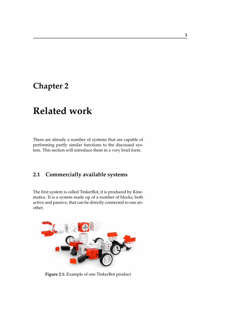
The first system is called TinkerBot, it is produced by Kine-matics. It is a system made up of a number of blocks, bothactive and passive, that can be directly connected to one an-other.
Figure 2.1: Example of one TinkerBot product
4 2 Related work
The square red-orange cube, in the upper middle of the fig-ure, is called the Powerbrain. It is similar to the board, seeSection 3.3. It is responsible for controlling the individualsensor and actuator blocks while at the same time it is pro-viding power to the individual modules. The only informa-tion about how the communication is handled is found ontheir indiegogo page. It is said there, that the Powerbrainuses a Serial UART bus-system for communication. Furthermore, the Powerbrain is also capable to communicate withmobile devices via Bluetooth.There are only motion focused actuators such as a motor, atilting joint, one that is akin to a servo and a gripper. Thereis a distance and a light sensor for input. The Powerbrainalso contains a three axis accelerometer and gyroscope.The whole system runs on a built-in lithium polymer bat-tery.
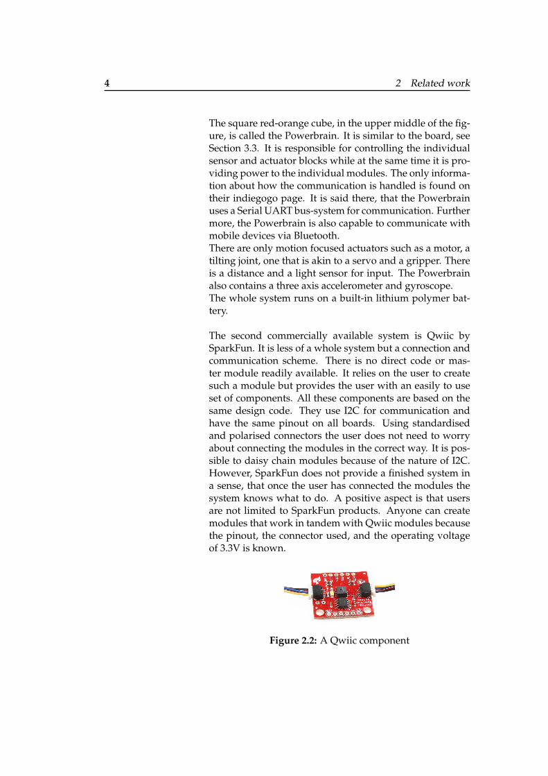
The second commercially available system is Qwiic bySparkFun. It is less of a whole system but a connection andcommunication scheme. There is no direct code or mas-ter module readily available. It relies on the user to createsuch a module but provides the user with an easily to useset of components. All these components are based on thesame design code. They use I2C for communication andhave the same pinout on all boards. Using standardisedand polarised connectors the user does not need to worryabout connecting the modules in the correct way. It is pos-sible to daisy chain modules because of the nature of I2C.However, SparkFun does not provide a finished system ina sense, that once the user has connected the modules thesystem knows what to do. A positive aspect is that usersare not limited to SparkFun products. Anyone can createmodules that work in tandem with Qwiic modules becausethe pinout, the connector used, and the operating voltageof 3.3V is known.
Figure 2.2: A Qwiic component
2.2 Academic systems 5
2.2 Academic systems
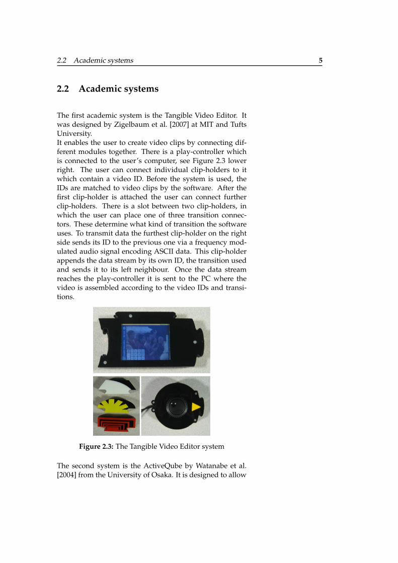
The first academic system is the Tangible Video Editor. Itwas designed by Zigelbaum et al. [2007] at MIT and TuftsUniversity.It enables the user to create video clips by connecting dif-ferent modules together. There is a play-controller whichis connected to the user’s computer, see Figure 2.3 lowerright. The user can connect individual clip-holders to itwhich contain a video ID. Before the system is used, theIDs are matched to video clips by the software. After thefirst clip-holder is attached the user can connect furtherclip-holders. There is a slot between two clip-holders, inwhich the user can place one of three transition connec-tors. These determine what kind of transition the softwareuses. To transmit data the furthest clip-holder on the rightside sends its ID to the previous one via a frequency mod-ulated audio signal encoding ASCII data. This clip-holderappends the data stream by its own ID, the transition usedand sends it to its left neighbour. Once the data streamreaches the play-controller it is sent to the PC where thevideo is assembled according to the video IDs and transi-tions.
Figure 2.3: The Tangible Video Editor system
The second system is the ActiveQube by Watanabe et al.[2004] from the University of Osaka. It is designed to allow
6 2 Related work
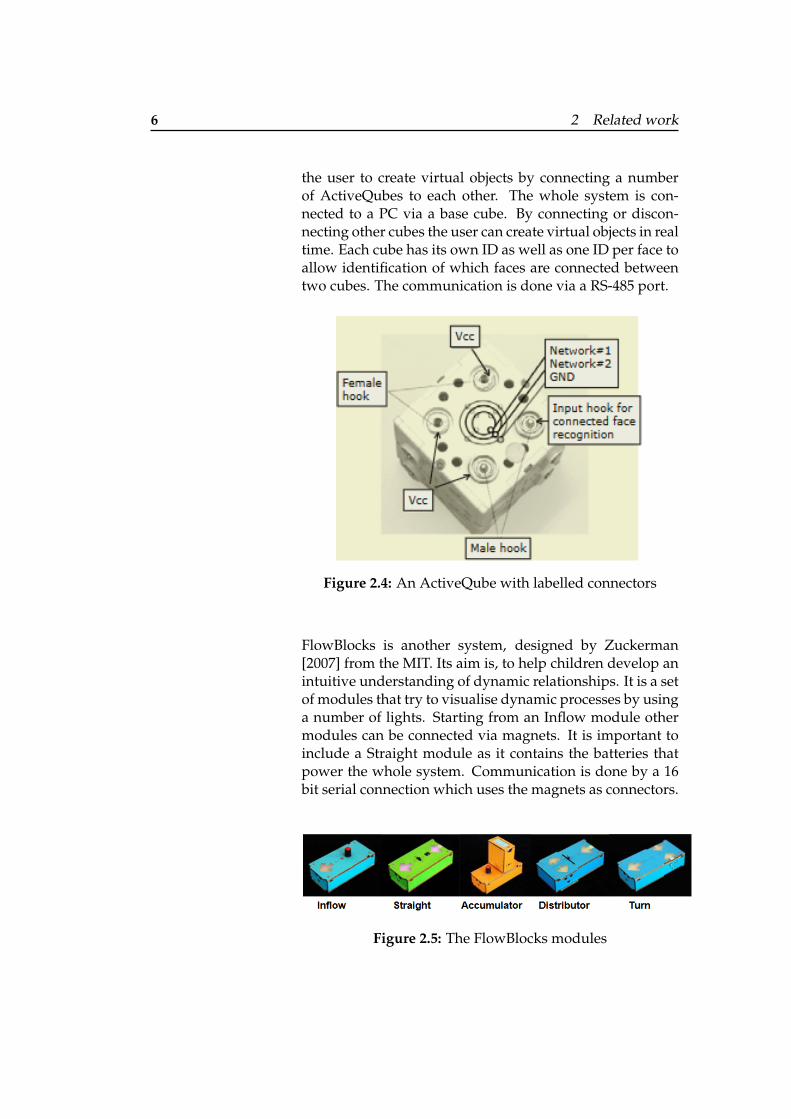
the user to create virtual objects by connecting a numberof ActiveQubes to each other. The whole system is con-nected to a PC via a base cube. By connecting or discon-necting other cubes the user can create virtual objects in realtime. Each cube has its own ID as well as one ID per face toallow identification of which faces are connected betweentwo cubes. The communication is done via a RS-485 port.
Figure 2.4: An ActiveQube with labelled connectors
FlowBlocks is another system, designed by Zuckerman[2007] from the MIT. Its aim is, to help children develop anintuitive understanding of dynamic relationships. It is a setof modules that try to visualise dynamic processes by usinga number of lights. Starting from an Inflow module othermodules can be connected via magnets. It is important toinclude a Straight module as it contains the batteries thatpower the whole system. Communication is done by a 16bit serial connection which uses the magnets as connectors.
Figure 2.5: The FlowBlocks modules
2.2 Academic systems 7
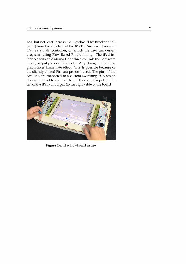
Last but not least there is the Flowboard by Brocker et al.[2019] from the i10 chair of the RWTH Aachen. It uses aniPad as a main controller, on which the user can designprograms using Flow-Based Programming. The iPad in-terfaces with an Arduino Uno which controls the hardwareinput/output pins via Bluetooth. Any change in the flowgraph takes immediate effect. This is possible because ofthe slightly altered Firmata protocol used. The pins of theArduino are connected to a custom switching PCB whichallows the iPad to connect them either to the input (to theleft of the iPad) or output (to the right) side of the board.
Figure 2.6: The Flowboard in use

9
Chapter 3
Own work
The goal of this thesis was to create a user-friendly wear-able networking system. It consists of a main board, whichhandles the networking and a number of chips which canbe placed at any connection point at any time. This sectionexplains the software requirements and the reasons whya UART Serial communication was chosen. Afterwards itintroduces the board, explains why an Arduino MKR1000was used as the main microcontroller and explains what isneeded for the communication. The section closes by dis-cussing the chips designed so far and what challenges arosein the design process.
3.1 Requirements
There were certain requirements for the system that had tobe met: First the system had to be able to communicatewith multiple chips. An appropriate communication pro-tocol had to be chosen for that. A weak point in each wear-able system are the connectors and connections, as they en-dure the most stress, either from frequent connecting anddisconnecting, or from bending while wearing it. Becauseof this the goal was to minimise the number of connectionsneeded. For that reason SPI was excluded from the begin-ning. The two remaining protocols which are supported by
10 3 Own work
the AtTiny are I2C and Serial. The decision process is ex-From here on theterm Serial refers to
the UART Serialcommunication
protocol
plained in the section below.
For the first mode the system does not need to know wherethe chips are located, however, it is imperative for the sec-ond mode. For that the system needs a way to find andstore the location of any connected chip.
The chip requirements were very simple. Aside from thepinout described in Section 3.4 and the wish to use an At-Tiny85 there were no other requirements.
3.1.1 I2C vs. Serial
I2C and Serial are both protocols that are usually directlysupported by the hardware of most microprocessors. Thisand the fact, that they are fairly simple and only use twopins, make them the best choices for infrequent and, com-pared to SPI, slow data communication. This section willexplain the reasons why Serial was chosen instead of I2C.
The I2C communication protocol is a master/slave system.It uses a two-wire-bus: the first wire carries a clock whilethe second carries the data signals. It uses a 7 bit addressfor each module, thus there are 127 different possible ad-dresses. Each module is connected to the same bus.The reasons why I2C is not a suitable candidate for the sys-tem lies within the master/slave setup of the protocol. Inthis configuration only the master is able to initiate the com-munication. This disqualified I2C because the chips weresupposed to be able to start sending data as soon as theyget them. Another draw back of I2C is that each module,that is connected to the bus, needs to have a unique ad-dress. It should be possible to connect chips with the sameaddress to the board.
The Serial communication protocol also uses two wires, butinstead of using one wire for a clock signal Serial uses bothfor data transmission. Each is carrying the communicationin one direction. Thus the sender of one module (called tx,short for transmitter) is connected to the receiver (called rx)
3.2 Early Work 11
of the other and vice versa. In contrast to I2C both modulescan start to send data at any time. The data is buffered untilthe receiver reads it. As Serial communication is only be-tween two modules there is no need for an address.That is a disadvantage of Serial compared to I2C. Serialcommunication is only between exactly two participants.In theory, it is possible to connect each tx pin to each rx pinof all the other modules. In praxis, this would not scale tomore than a couple of modules.
Serial was chosen as the chips should be able to initialisedata transmission as well as the board. My task was to finda way around the limitation.
3.2 Early Work
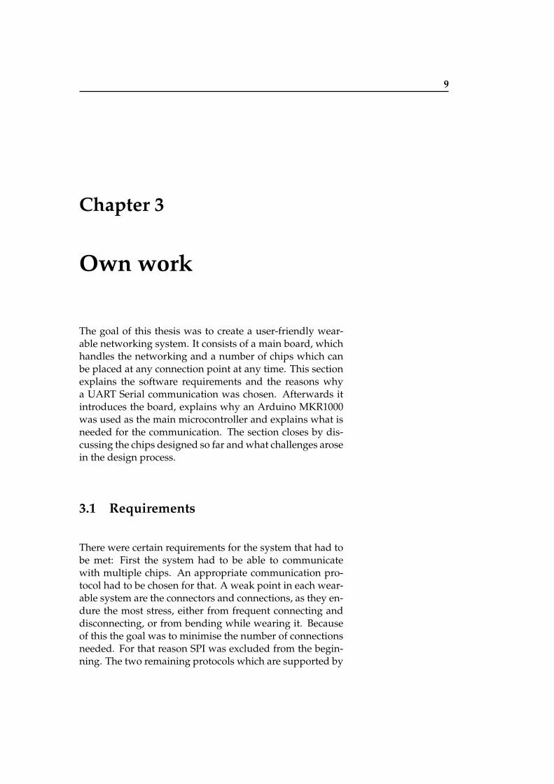
A first attempt was to use the Arduino SoftwareSerial li-brary and simply combine both the sender and receiverfunction at the same pin. This would, in theory, producea bus, like I2C uses, and cut down the numbers of pinsneeded, which would in turn increase the number of usablepins at the AtTiny.
Figure 3.1: Attempt for one wire communication
This did not work. In theory, all that had to be done wasto change the pin from receiver to sender each time thechip had to send data. In praxis, the write buffer needed
12 3 Own work
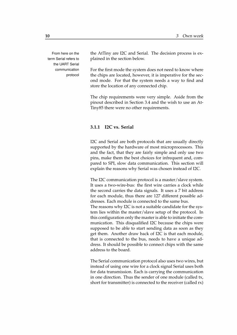
to be cleared before this could happen. There is a function,called flush(), within the SoftwareSerial library. However,this function only clears the input buffer. As SoftwareSerialis not intended for duplex use, it does not need to be ableto clear the write buffer.There exists a library called SoftwareSerialWithHalfDuplexby the user nickstedman on GitHub. This library had im-plemented all that was needed. It offered Serial communi-cation with half duplex over one wire.After a positive test with two Arduino Nanos communica-tion over one wire was also successful with a combinationof four AtTiny and one Arduino Nano.
Figure 3.2: Successful one wire communication
Addresses similar to I2C were used to identify the micro-processors. Each microcontroller got a character as an ad-dress assigned. In front of each data byte the sender had toplace one byte containing the address character. Each othermicrocontroller read the address byte as soon as it had ar-rived, compared it to its own address and decided whetherthe data, that it had read directly after the address, was in-tended for it or not.
3.3 Board
The main microcontroller will be called the board from nowon. It handles all the communication by checking where in-coming data is from and readdressing it to the correct chip,according to the selected mode. Beside communication it is
3.3 Board 13
also responsible for localising chips, which are connected toit, as well as handling the button, which changes the mode.
3.3.1 Upgrade
Before progressing any further from the state, described atthe end of the last section, and keeping the user-friendlyaspect in mind, the decision was made against using an Ar-duino Nano as the main microcontroller. To allow for morecomplex programs and the addition of further hardware,which need more RAM space, the decision was made toupgrade. Another deciding factor was, that while it is pos-sible to have multiple SoftwareSerial ports in the system,it is not possible to have them all listen at the same time.So if in the future the need arises to have multiple buses, asystem that uses SoftwareSerial will not work.
The choice was made to use the Arduino MKR1000 (for bet-ter readability called MKR). It has 32kb of RAM comparedto 2kb of the Nano and the possibility to configure multi-ple hardware serial ports. It is, however, no longer an AVRchip.It was no longer possible to use the SoftwareSerialWith-HalfDuplex library, on which the whole setup was relying,because the MKR uses an ARM chip.
The first test was simply to connect the tx pin of the MKRto all the rx pins of the Arduino Nanos and to connect allthe Nanos tx pins together to the rx pin of the MKR. Asthe chips do not need to send data directly to each other,they do not need connections between them. This was onlypartly successful. The MKR was able to send data to all theNanos, but the other way round did not work.This behaviour is caused by electric impedance. A sin-gle Nano is not able to drive the communication line lowenough when there is more than one receiver. However,this challenge can be overcome by using a simple diode (inthis case a 1N4148 signal diode), creating the impression foran individual Nano, that there is no other communicationpartner than the MKR.
14 3 Own work
3.3.2 Localisation
The initial idea was to localise chips, which are connectedto the board, by using a similar technique as used to drivea LED dot matrix. The connections were organised in amatrix form with rows and columns. By applying 5V andground accordingly, it is possible to select a specific locationin the matrix. If a chip is connected to this location, the chipboots up and sends its address, from now on called ID. Ifthe MKR does not receive an ID after 50ms, it knows, thatthere is no chip at this location and will check the next one.After this localisation step there were challenges expected,when all chips are supplied with power again. The chipsare not able to differentiate whether they are powered, be-cause the board tries to localise them, or if they should re-turn to normal operation. Thus all chips always send theirIDs when supplied with power. The intended solution was,that the MKR ignores any data coming in for a short periodafter switching on all chips.
However, this solution was never implemented. TheAtTinys were not able to successfully send their ID afterpowering up.At first the chips were directly powered by a pin of a Ar-duino Nano. It was uncertain whether the power suppliedwas powerful or stable enough. To stabilise it, a capacitorwas placed parallel to the chip. Another try was, to powerthe chip via a MOSFET directly from the power supply.Another possible cause for that behaviour might have beenthat there were some terminal characters in the incomingdata. All available methods for sending data were tried, aswell as clearing the buffer after reading the first byte.
3.3 Board 15
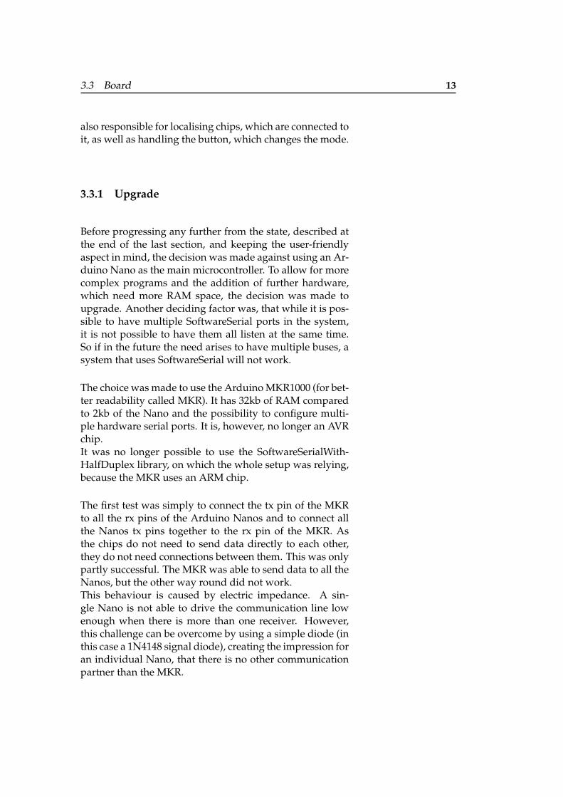
Figure 3.3: Evolution of the location test setup
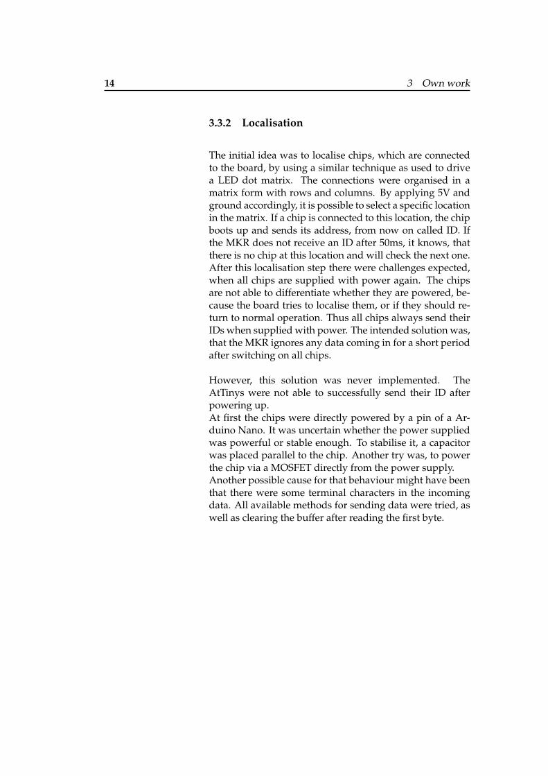
As the booting process does not allow for precisely timedintervals and might cause power fluctuations this approachwas discarded.As a new approach two wires were directly connected topins on the chip. If these wires are pulled low, the chip willsend its ID without the need to boot again.To reduce the number of pins needed, a 4011 NAND ICwas included, which leaves two pins on the AtTiny free tohandle its tasks.
Figure 3.4: Schematic of the finished board
16 3 Own work
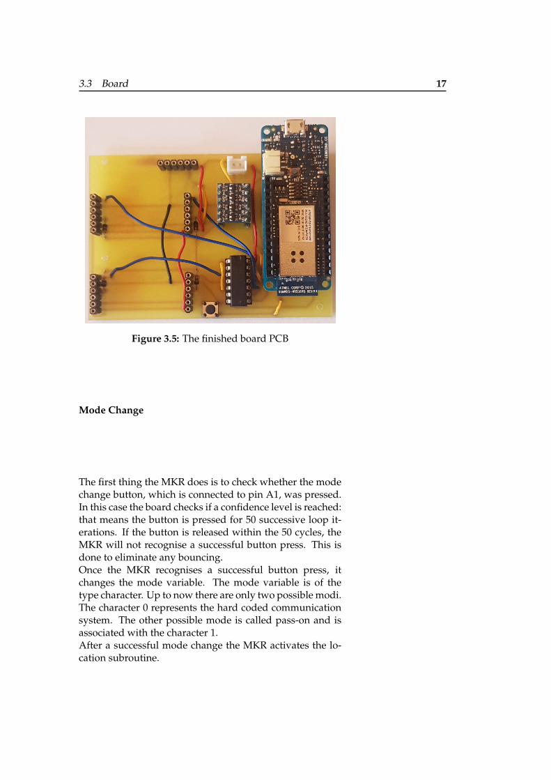
3.3.3 Hardware
Besides the above explained functions the board needssome additional components. Because the MKR is a 3.3Vmicrocontroller and can not handle 5V, which the AtTinysuse, the communication between both controllers is notpossible without level shifting.
In addition to the level shifter (the red rectangular in Figure3.4) there are five sockets on the board: four of these arefor connecting regular chips. Above these four there is anextra socket. This one is special, as it is not connected toany localisation line. Therefore, any chip connected with itwill not be found by the localisation routine of the MKR.This socket is intended for a display chip, see Section 3.4.2.
There is also a tactile switch above the MKR. It is connectedto the MKR via an internal pullup resistor. By pressing thisbutton the communication mode is changed. For more in-formation about these modi see the next section.
Last there is a JST for the power connection. A micro USBJST = JapaneseSolderless Terminal
(0.1in pitch)port is the intended way to supply power, but if the userwants to use a different power source, he simply needs toconnect it via this JST. The JST ensures, that it is not possibleto connect the power source the wrong way. The boardsoperational voltage is 5V.
3.3.4 Software
In this section the software which is operating the boardwill be discussed. There are three main components. Thefirst thing the software checks is, whether the mode changebutton is pressed and acts accordingly. After that the soft-ware handles any incoming data. The last part checks ifthere is a change in the connected chips.While booting, the board initialises the second hardwareSerial port and reserves memory for the location array,which will contain the location of connected chips. It alsochecks if there is a Serial connection to a PC. If there is none,it tries to find a connection for five seconds.
3.3 Board 17
Figure 3.5: The finished board PCB
Mode Change
The first thing the MKR does is to check whether the modechange button, which is connected to pin A1, was pressed.In this case the board checks if a confidence level is reached:that means the button is pressed for 50 successive loop it-erations. If the button is released within the 50 cycles, theMKR will not recognise a successful button press. This isdone to eliminate any bouncing.Once the MKR recognises a successful button press, itchanges the mode variable. The mode variable is of thetype character. Up to now there are only two possible modi.The character 0 represents the hard coded communicationsystem. The other possible mode is called pass-on and isassociated with the character 1.After a successful mode change the MKR activates the lo-cation subroutine.
18 3 Own work
Communication
After handling a possible button press the MKR checksboth Serial ports.
The native Serial port might be connected to a PC. If it is notconnected, there will never be any data and the MKR willnever enter this subroutine. If there is data, it will either bethe single character t, which will prompt the MKR to jumpinto the localisation subroutine, or if it is not, the MKR willtry to read a second character and send this to the chip withan address matching the first read byte.
After checking the native Serial port the MKR will check thesecond one. This is the one connected to the sockets and thechips. If there is data, the MKR expects two bytes. The firstbyte contains the address of the chip, which has sent thedata, while the second byte is the data itself. If there is nosecond data byte, the MKR will simply put in the characterx as data.Having received data, the MKR checks the mode variableto determine which communication mode to use.
The simpler mode is the hardcoded one. In this mode theMKR sends the data, based on the senders ID, according toa hardcoded lookup table to the receiver.
The pass-on mode is a little more complex. After receiv-ing data, the MKR checks in the location array, whether theposition of the sender is known. If it is unknown, it willjump into the localisation subroutine to find the position. Ifit is still not able to find the position, it will discard the datapackage.If it finds the sender’s location, the board will look up theID of the chip at the next higher position. After that, it sim-ply sends the data to that chip. If there is no chip in the nextposition, it will discard the package as well.
3.4 Chips 19
Localisation Routine
The localisation subroutine will only be called every fiveseconds if it is not called by one of the two others. It hastwo parts. The first is responsible for finding the chips, thesecond sends data to a display chip, see Section 3.4.2.
The positions are arranged in a matrix form. By using thisconfiguration the board is able to use only the number ofrows + columns pins, to check rows ∗ columns positions.
The first step is to pull the lines going to the correspondingposition high. Which in turn will pull the location line go-ing from the 4011 NAND to the chip low. The board waitsfor 50ms, before it checks, whether there is an ID message atthe second Serial port. If there is a message, the MKR willstore the ID in the locations array, otherwise it will placethe character x, to indicate that the position is empty. After-wards it repeats this procedure for all possible locations.
After checking all locations the subroutine will try to sendthe new locations array via the native Serial port to a con-nected computer as well as to a display chip. The data forthe display chip is extended by the byte representing themode.
3.4 Chips
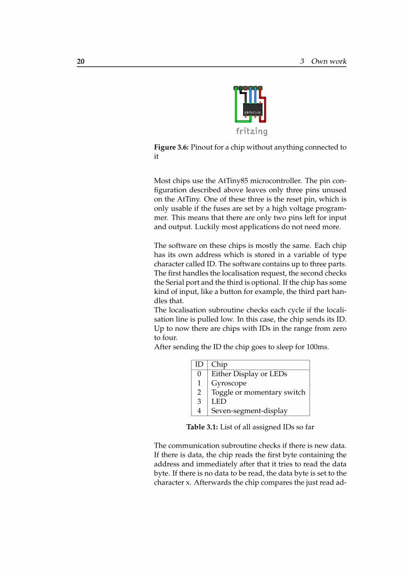
The different chips are introduced in this section. All chipshave the same pinout to connect to the board, therefore, theuser can connect each chip to each location.The chip, the right side up, the pins on the top, startingfrom the left pin: the first is the localisation pin, if that one ispulled low, the chip sends its ID to the board. The next pinis ground. After that there is an empty pin, which makesthe connector not symmetrical and prevents the user fromaccidentally placing the chip in the wrong direction. Thenext two pins are the communication pins. The last pin isthe voltage supply.
20 3 Own work
Figure 3.6: Pinout for a chip without anything connected toit
Most chips use the AtTiny85 microcontroller. The pin con-figuration described above leaves only three pins unusedon the AtTiny. One of these three is the reset pin, which isonly usable if the fuses are set by a high voltage program-mer. This means that there are only two pins left for inputand output. Luckily most applications do not need more.
The software on these chips is mostly the same. Each chiphas its own address which is stored in a variable of typecharacter called ID. The software contains up to three parts.The first handles the localisation request, the second checksthe Serial port and the third is optional. If the chip has somekind of input, like a button for example, the third part han-dles that.The localisation subroutine checks each cycle if the locali-sation line is pulled low. In this case, the chip sends its ID.Up to now there are chips with IDs in the range from zeroto four.After sending the ID the chip goes to sleep for 100ms.
ID Chip0 Either Display or LEDs1 Gyroscope2 Toggle or momentary switch3 LED4 Seven-segment-display
Table 3.1: List of all assigned IDs so far
The communication subroutine checks if there is new data.If there is data, the chip reads the first byte containing theaddress and immediately after that it tries to read the databyte. If there is no data to be read, the data byte is set to thecharacter x. Afterwards the chip compares the just read ad-
3.4 Chips 21
dress with its own ID. If they match, it knows, that the datawas intended for itself and can act accordingly. Otherwiseit ignores the data byte.
As the third part is optional, it is individual to the specificchip and will be discussed in the section corresponding tothe chip.
3.4.1 Simple Chips
Simple chips are chips, that do not rely on a communica-tion protocol to get their data from their sensor or to get itto the actuator. At the moment there are two chips of thiscategory.
Button
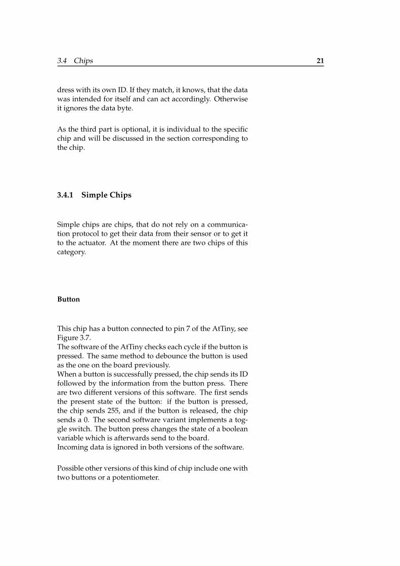
This chip has a button connected to pin 7 of the AtTiny, seeFigure 3.7.The software of the AtTiny checks each cycle if the button ispressed. The same method to debounce the button is usedas the one on the board previously.When a button is successfully pressed, the chip sends its IDfollowed by the information from the button press. Thereare two different versions of this software. The first sendsthe present state of the button: if the button is pressed,the chip sends 255, and if the button is released, the chipsends a 0. The second software variant implements a tog-gle switch. The button press changes the state of a booleanvariable which is afterwards send to the board.Incoming data is ignored in both versions of the software.
Possible other versions of this kind of chip include one withtwo buttons or a potentiometer.
22 3 Own work
Figure 3.7: Schematic of the button chip
LED
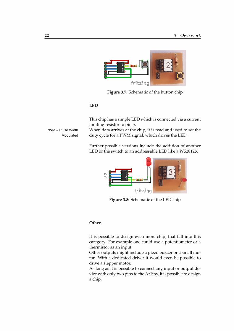
This chip has a simple LED which is connected via a currentlimiting resistor to pin 5.When data arrives at the chip, it is read and used to set thePWM = Pulse Width
Modulated duty cycle for a PWM signal, which drives the LED.
Further possible versions include the addition of anotherLED or the switch to an addressable LED like a WS2812b.
Figure 3.8: Schematic of the LED chip
Other
It is possible to design even more chip, that fall into thiscategory. For example one could use a potentiometer or athermistor as an input.Other outputs might include a piezo buzzer or a small mo-tor. With a dedicated driver it would even be possible todrive a stepper motor.As long as it is possible to connect any input or output de-vice with only two pins to the AtTiny, it is possible to designa chip.
3.4 Chips 23
3.4.2 I2C Chips
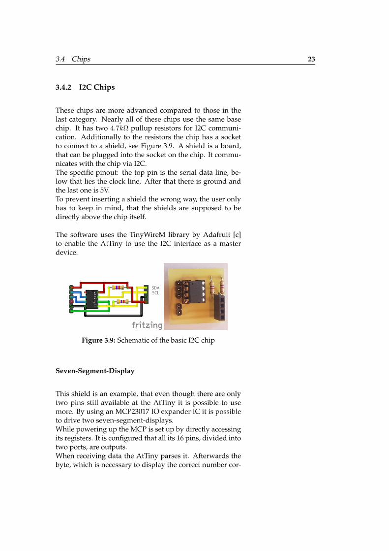
These chips are more advanced compared to those in thelast category. Nearly all of these chips use the same basechip. It has two 4.7kΩ pullup resistors for I2C communi-cation. Additionally to the resistors the chip has a socketto connect to a shield, see Figure 3.9. A shield is a board,that can be plugged into the socket on the chip. It commu-nicates with the chip via I2C.The specific pinout: the top pin is the serial data line, be-low that lies the clock line. After that there is ground andthe last one is 5V.To prevent inserting a shield the wrong way, the user onlyhas to keep in mind, that the shields are supposed to bedirectly above the chip itself.
The software uses the TinyWireM library by Adafruit [c]to enable the AtTiny to use the I2C interface as a masterdevice.
Figure 3.9: Schematic of the basic I2C chip
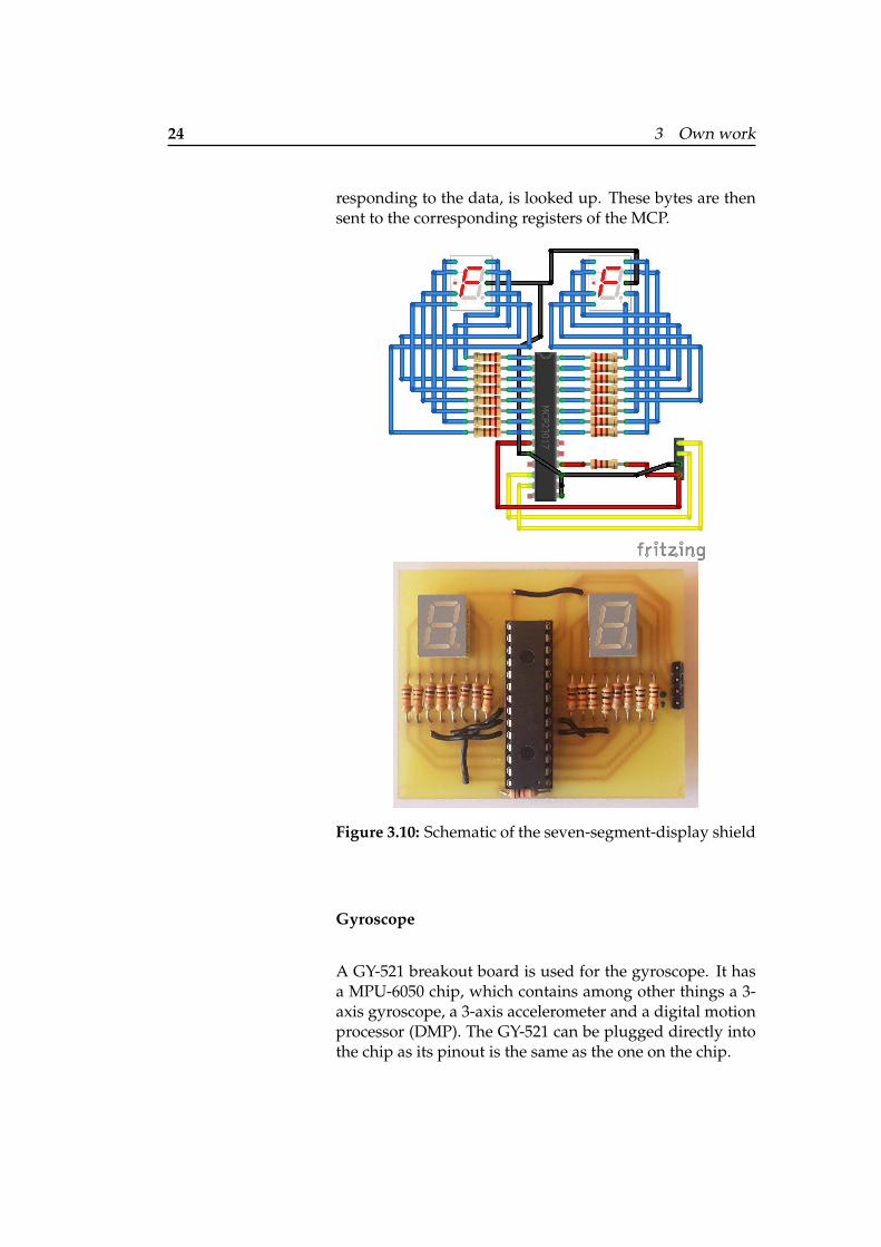
Seven-Segment-Display
This shield is an example, that even though there are onlytwo pins still available at the AtTiny it is possible to usemore. By using an MCP23017 IO expander IC it is possibleto drive two seven-segment-displays.While powering up the MCP is set up by directly accessingits registers. It is configured that all its 16 pins, divided intotwo ports, are outputs.When receiving data the AtTiny parses it. Afterwards thebyte, which is necessary to display the correct number cor-
24 3 Own work
responding to the data, is looked up. These bytes are thensent to the corresponding registers of the MCP.
Figure 3.10: Schematic of the seven-segment-display shield
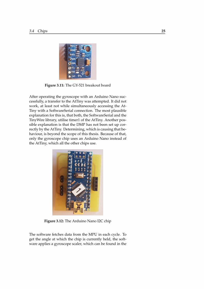
Gyroscope
A GY-521 breakout board is used for the gyroscope. It hasa MPU-6050 chip, which contains among other things a 3-axis gyroscope, a 3-axis accelerometer and a digital motionprocessor (DMP). The GY-521 can be plugged directly intothe chip as its pinout is the same as the one on the chip.
3.4 Chips 25
Figure 3.11: The GY-521 breakout board
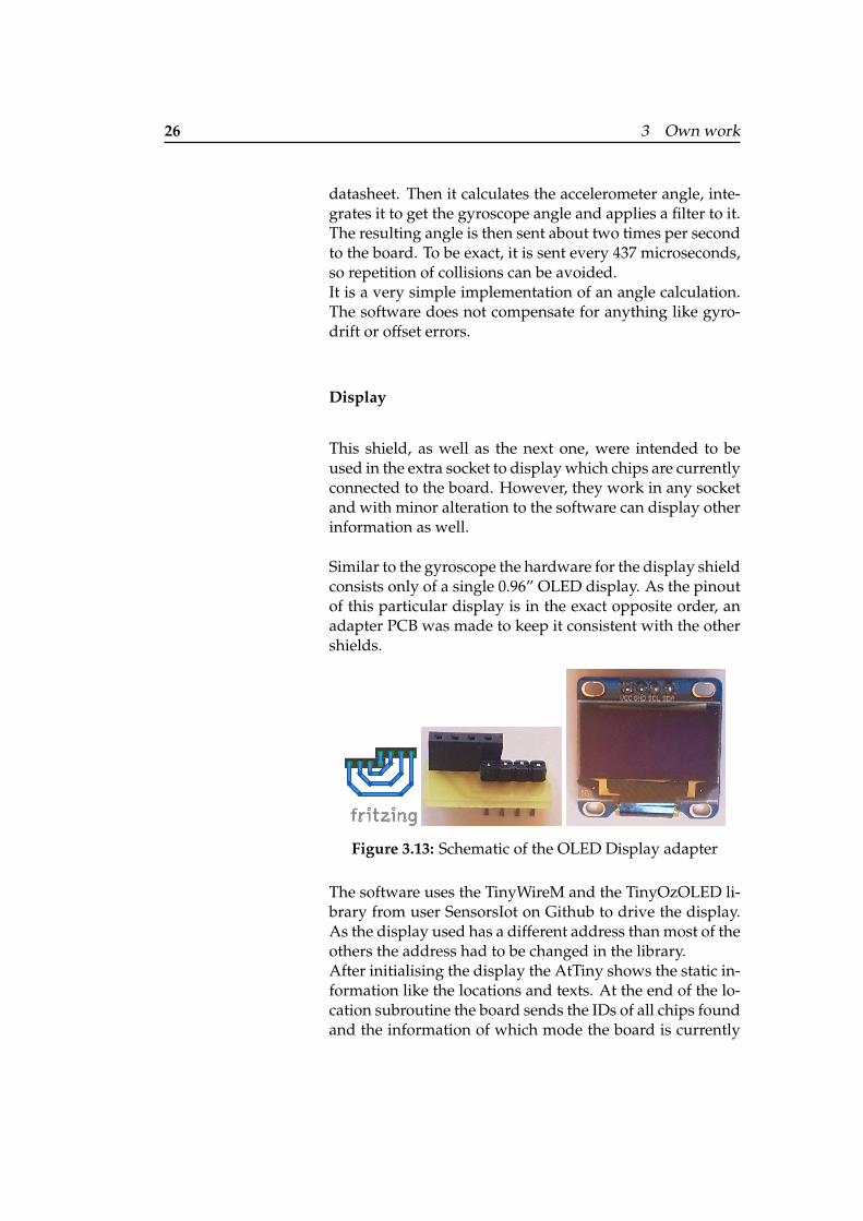
After operating the gyroscope with an Arduino Nano suc-cessfully, a transfer to the AtTiny was attempted. It did notwork, at least not while simultaneously accessing the At-Tiny with a SoftwareSerial connection. The most plausibleexplanation for this is, that both, the SoftwareSerial and theTinyWire library, utilise timer1 of the AtTiny. Another pos-sible explanation is that the DMP has not been set up cor-rectly by the AtTiny. Determining, which is causing that be-haviour, is beyond the scope of this thesis. Because of that,only the gyroscope chip uses an Arduino Nano instead ofthe AtTiny, which all the other chips use.
Figure 3.12: The Arduino Nano I2C chip
The software fetches data from the MPU in each cycle. Toget the angle at which the chip is currently held, the soft-ware applies a gyroscope scaler, which can be found in the
26 3 Own work
datasheet. Then it calculates the accelerometer angle, inte-grates it to get the gyroscope angle and applies a filter to it.The resulting angle is then sent about two times per secondto the board. To be exact, it is sent every 437 microseconds,so repetition of collisions can be avoided.It is a very simple implementation of an angle calculation.The software does not compensate for anything like gyro-drift or offset errors.
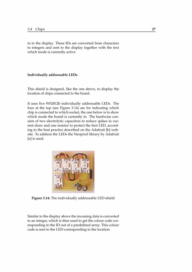
Display
This shield, as well as the next one, were intended to beused in the extra socket to display which chips are currentlyconnected to the board. However, they work in any socketand with minor alteration to the software can display otherinformation as well.
Similar to the gyroscope the hardware for the display shieldconsists only of a single 0.96” OLED display. As the pinoutof this particular display is in the exact opposite order, anadapter PCB was made to keep it consistent with the othershields.
Figure 3.13: Schematic of the OLED Display adapter
The software uses the TinyWireM and the TinyOzOLED li-brary from user SensorsIot on Github to drive the display.As the display used has a different address than most of theothers the address had to be changed in the library.After initialising the display the AtTiny shows the static in-formation like the locations and texts. At the end of the lo-cation subroutine the board sends the IDs of all chips foundand the information of which mode the board is currently
3.4 Chips 27
in to the display. These IDs are converted from charactersto integers and sent to the display together with the textwhich mode is currently active.
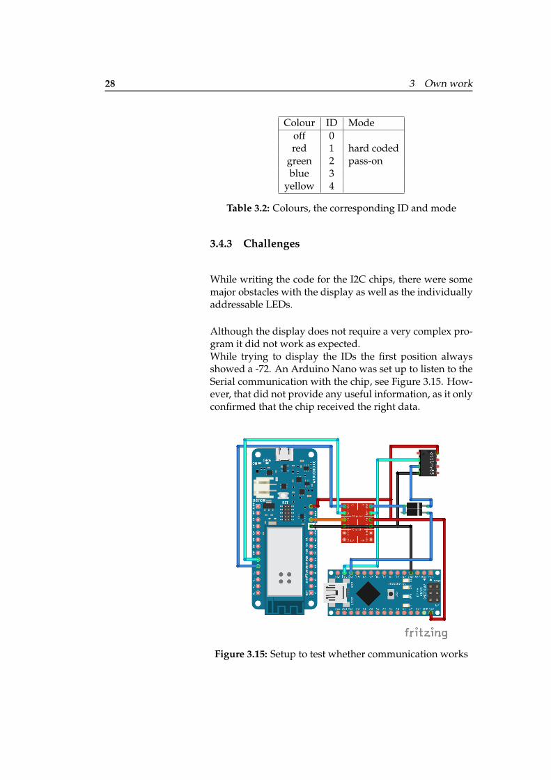
Individually addressable LEDs
This shield is designed, like the one above, to display thelocation of chips connected to the board.
It uses five WS2812b individually addressable LEDs. Thefour at the top (see Figure 3.14) are for indicating whichchip is connected to which socket, the one below is to showwhich mode the board is currently in. The hardware con-sists of two electrolytic capacitors to reduce spikes in cur-rent draw and one resistor to protect the first LED, accord-ing to the best practice described on the Adafruit [b] web-site. To address the LEDs the Neopixel library by Adafruit[a] is used.
Figure 3.14: The individually addressable LED shield
Similar to the display above the incoming data is convertedto an integer, which is then used to get the colour code cor-responding to the ID out of a predefined array. This colourcode is sent to the LED corresponding to the location.
28 3 Own work
Colour ID Modeoff 0red 1 hard coded
green 2 pass-onblue 3
yellow 4
Table 3.2: Colours, the corresponding ID and mode
3.4.3 Challenges
While writing the code for the I2C chips, there were somemajor obstacles with the display as well as the individuallyaddressable LEDs.
Although the display does not require a very complex pro-gram it did not work as expected.While trying to display the IDs the first position alwaysshowed a -72. An Arduino Nano was set up to listen to theSerial communication with the chip, see Figure 3.15. How-ever, that did not provide any useful information, as it onlyconfirmed that the chip received the right data.
Figure 3.15: Setup to test whether communication works
3.4 Chips 29
After programming the chip to send back all data beforedisplaying it, it became clear that the information receivedby the chip was corrupted somewhere between the socketon the board and the part of the software that displayed it.By not connecting the chip in the extra socket but in one ofthe four standard ones it was possible to check if the wiringwas correct. As the chip functioned flawlessly at this posi-tion, it was clear that there was a wiring problem. The onlydifference from the standard to the extra socket was that atthe extra socket the localisation line was not connected.After connecting the localisation line of the extra socket to5V the chip worked at that location as well.
Similar to the display above the individually address-able LEDs did not initially work as intended. After re-ceiving data the shield displayed the right colours at theright places, but after less than one second the colourschanged. The colours which were then displayed werecolours not among the preconfigured ones. These wrongcolours stayed until the chip got the next message from theboard. After swapping the chips at the board the first dis-played colours were also changed correctly. But again afterless than a second the colours changed to the previouslywrong ones. Altering the program the same way as thesoftware of the display shield the chip now sent the data,which it tried to display on the LEDs, to the board.It turned out that the chip received another data set afterthe correct one. The monitoring of the data transmissionproved that there was only the correct data on the bus.The solution was to check, before sending data to the LEDs,whether the data is a known ID or not.

31
Chapter 4
Evaluation
The goal of this thesis was to create a user-friendly wear-able networking system. This chapter is going to evalu-ate which of these three aspects were sufficiently met andwhich need to be improved.
4.1 User-friendliness
There are many aspects to consider whether a system isuser-friendly or not.
Does the system require any additional parts that are notincluded?The only thing, the user has to provide, is a power source.He is free to choose what kind of power supply he wantsto use. He can use the provided micro USB port to power itfrom any USB power supply, or he can disconnect this portform the JST and connect any other power supply there, aslong as it is capable of providing a stable 5V.
If there are connectors, is it possible to connect them thewrong way and destroy any electrical components?Most connectors in the system are designed in a way thatit is physically impossible to connect them the wrong way.The connectors between board and chips are asymmetrical,
32 4 Evaluation
so there is no way to force them into the socket the wrongway. For the power connector the board uses a JST withregistration teeth which prohibit wrong insertion.The only parts that can be connected in a way not intendedare the shields for the I2C chips. However, they are de-signed in a way, that the user only has to remember, thatthe shield has to be directly above the chip. If he forgetsthis, the power pins are located in such a way that it is stillimpossible to connect ground to 5V and vice versa.
Does it matter which chip is connected to which location?And can the location be changed at any moment?This depends on the mode the user chooses. After theboard has powered up it is in the hardcoded mode. In thismode it does not matter where a chip is connected and thesystem checks, only based on the senders ID, to which chipthe message is supposed to go. That means, that it is pos-sible to connect and disconnect any chip at any given time,because even if the addressed chip is not there, the messageis sent anyway.In the second mode the user has to keep in mind that thechips, which he wants to communicate, have to be directlynext to one another. Although this is more complex it of-fers more options. New setups can be created without theneed to change the software. In this mode chips can also beconnected and disconnected at any given moment. Beforesending the data the system always checks the sender’s lo-cation and if there is a chip in the next position to which thedata will be addressed.Although the above introduced system works there aresome aspects to be improved, see Section 5.2 for ideas.
Does the system provide information about which chip isconnected to which location?The board has an extra socket to connect a display chip.Up to now there are two kinds of displays: a 0.96” OLEDdisplay which can show the positions, the connected chipsand which mode the board is in. The other option is theWS2812b individually addressable LED shield. It displays,which chip is connected to which position by assigningeach ID its own colour and by displaying that colour at theLED corresponding to its location. The mode is displayedin the same way.
4.2 Wearability 33
If the user wants, he can create other methods for display-ing the information.
Is it possible to create new chips?The user can create as many chips as he needs. He has touse the same pinout as described in the chip section. Hehas to keep the communication format, first sending thechips ID followed by a data byte. The chip has to be ableto handle the information sent by the board, this includesthe capability to handle the longer data stream containingthe location information for the displays. But otherwise theuser can create any chip he wants or needs. He is not evenrestricted to the use of the AtTiny85.
4.2 Wearability
The system needs to be small enough to be comfortableto wear, it needs to be self contained and to have its ownpower source. All these aspects are met successfully, how-ever, there is still room for improvements, see Section 5.2.At the moment the board has a maximum length of 9.5cmat a width of 6.5cm, which makes it smaller than most mod-ern smart-phones. Even if it is in a case, the user is able tocarry it comfortably attached to a belt or in a pocket. Thechips use the AtTiny85 to keep them as small as possible.
The system does not require any external hardware to oper-ate except for the power supply. While booting, the boardchecks whether there is a Serial connection to a computer,however, that is only to provide the user with additionalinformation: such as which chip sent what kind of data. Ifthere is no connection, the system will still operate perfectlywithout one.
The system uses a micro USB socket as a power connectorto provide it with power. Using a powerbank is the sim-plest way. These are available in many different sizes andshapes, so the user can choose the one that he prefers.
34 4 Evaluation
4.3 Networking
The most interesting part of this work was the networking.As described in Section 3.2 the initial idea was to combineboth communication lines into a single one. This is possi-ble as long as the system uses an AVR chip. By utilising theSoftwareSerialWithHalfDuplex library it is feasible to havemultiple chips capable of communicating with one anotherover the same wire. The highest tested number of success-fully communicating microcontrollers was five. This is suf-ficient to create the desired networking.
A change was made to an ARM based processor because ofthe reasons described in Section 3.3.1. As there is no equiva-lent library for this processor architecture the whole systemneeded to be reworked. By using signal diodes it is possi-ble to create virtual communication channels which enableone chip to talk to the board without noticing that there aremultiple other chips connected. After adjusting the addressthe board simply broadcasts all messages it received to allconnected chips. Thus it appears to the chips that they com-municate with each other, although they do not know forwhich chip their message is or where that chip is located.
If the redirecting is hardcoded, the board will not have todo much. The board simply checks the senders ID andlooks up the correct receiver before broadcasting the data.Only the right receiver gets the data as all chips discardmessages that do not contain their ID. The board does thisregardless whether or not the correct chip is connected.
The more interesting part is redirecting based on the loca-tion of the sender. For this the board needs to know where asender is located. The board checks whether the location ofthe sender is known. If it is not, the board tries to find thatchip. After successfully locating the chip the board checkswhether there is a chip at the next position. If there is one,the data is sent to it. Otherwise the data is discarded.
Both modi implement valid networking strategies. The lasttask is to determine if there are not too many collisions forthe system to operate effectively. As collisions can only
4.3 Networking 35
happen if two chips try to send data at the same time, itis necessary to look at the rate at which the chips send data.The chip that sends most frequently data is the gyroscopechip. It sends data about two times per second. The line isoccupied for only 4.17 milliseconds if a boud rate of 9600is used and the chip sends two times 20 bit (2x(1startbit +8databits + 1stopbit)) per second. This means a collisioncan hardly happen. Even if one occurs, the damage is mostsurely corrected by the next data package sent by the gyro-scope.However, this might be improved in the future by imple-menting a system that either is able to detect if a collisionhappened or that is able to prevent them from occurring.

37
Chapter 5
Summary and futurework
5.1 Summary and contributions
This thesis dealt with two main goals. Primary to cre-ate a networking system and secondly to provide a user-friendly experience. The networking is done via a Serialport. By combining the transmitter lines of the connectedchips with the use of 1N4148 signal diodes it is possibleto have communication between two components even ifthere are more. The board offers two modi in which thenetworking is done. In the first mode the address corre-sponding to an incoming message is directly written intothe software of the board. The second mode offers moreflexibility. It redirects messages based on the location of thesender. The system is able to localise where a certain chipis connected.Each aspect is designed with user-friendliness in mind. Be-sides the possibility to have message-passing, either hard-coded or dependant on the position, the user is able to con-nect any chip at any location. He can connect or disconnectchips at any time and the system will adapt to it. The onlything the user has to think about is, if he uses pass-on mode,that chips which should communicate have to be locatednext to each other. The sockets on the board are designed
38 5 Summary and future work
in a way that it is impossible to connect a chip the wrongway. The whole board runs on 5V, it has a micro USB con-nector to power it. But if the user wants, he can connectany power supply to the board via a JST connector, as longas it provides a stable 5V. The user can create any chip heneeds because there is a blank chip template, see Figure 3.6.But he can also adapt more complex hardware to utilize thestandard I2C chip. The user has the option to connect a dis-play or individually addressable LEDs at the extra socketto show which chips are connected at which location.
Ideas to take away from this work: it is possible to use Se-rial communication which is designed to be a communica-tion protocol between two participants. But it can also beused to communicate with more than two if the communi-cation is done via a communication hub. Using diodes itis possible to simulate direct communication channels be-tween two members. However, depending on the rate atwhich data needs to be transmitted it is possible that colli-sions might occur.Another important point is that all input pins must be con-nected either to the supply voltage or to ground. If one isleft unconnected, this pin might cause havoc, even if thesoftware does not access it. If all pins are connected theright way, there might still occur some effects which needto be handled so that the software can run reliably, see Sec-tion 3.4.3.
5.2 Future work
For the future there are still some aspects that can be im-proved.The most important one would be to shrink the footprint ofall parts. Except from the MKR and the one Arduino Nano,which are already SMD and cannot easily be shrunk anySMD = surface
mounted device further, all parts are through-hole components. Replacingthem with SMD ones the size can be reduced significantly.This will increase the comfort for the user while wearingthe system.
Afterwards the next two points are of equal importance.
5.2 Future work 39
The addition of a third mode to the board: this one wouldbe a mix of the already existing two. This means that theuser has the possibility to hardcode the communication be-tween certain chips, while leaving some communication tobe determined by the location on the board. This would beuseful in the case that one chip is intended to work withanother specific one, like the seven-segment-display is in-tended to work with the gyroscope. The activation of thefirst chip (e.g. the gyroscope) can be determined by anychip (e.g. the button) which is placed in front of it. Asshown above it would be possible to use the button chipwith either the toggle or the momentary switch program.Another possibility: a chip with a potentiometer can beused to start the communication of the gyroscope if a cer-tain threshold value is reached.
Additionally to the third mode, the hardcoded mode canbe made a bit more user-friendly by changing the way thehardcoding is done. Up to now the user has to change thehardcoded list within the code. The user should be able tocreate a simple text document which is stored on a SD card.While booting, the board checks the text file and adjusts thedefinitions how incoming data is redirected to the chips.This could be done in a way that any connection, that is notspecified by the user, is treated as if the board is in pass-onemode.
The system can even be more expanded if more chips aredesigned. As mentioned in Section 3.4 there is nearly nolimit to the number of possible chips. Especially the cre-ation of a potentiometer chip would be advantageous. Itwould allow the user, for example, to control the rate atwhich the gyroscope chip is sending data or to define thebrightness of a LED.Besides the potentiometer, a SD card chip would be ex-tremely useful: either to log certain data or to read datafrom a file and use it to influence the behaviour of the sys-tem.For this purpose a totally new type of chip needs to be cre-ated as the AtTiny85 does not have a sufficient number ofpins for the SPI communication on which the SD card relies.It might be possible to create a SPI chip using the physicallybigger brother of the AtTiny85, the AtTiny84. If this proves
40 5 Summary and future work
to be impossible, one could still use an Arduino Nano tocreate such a chip.
Last the communication protocol should be changed signif-icantly. Up to now it is only possible to send a single byte ofinformation, aside from the case where the board sends thelocalisation data. The protocol should be changed in a waythat, after the chip sent its ID, it has to declare the numberof bytes that it intends to send. Thus it would be possible tohave chips that are capable to send and receive more com-plex data. This would be advantageous for a chip like thegyroscope, as it is limited to just one axis of rotation at themoment.
When the above mentioned points are changed or imple-mented one might start to think about a method to preventcollisions or at least to detect whether a collision has oc-curred.
The above described system offers an easy to use and quitecapable entry point into wearable electronics. Its modular-ity offers the user the possibility to experiment with differ-ent setups and configurations without previous knowledgein electronics. As the system is easily expandable, by cre-ating new modules, it is excellently suited for educationalpurposes on nearly every skill level.
41
Appendix A
Git
All software files can be found here: Software1
The hardware files are at this address: Hardware2
1https://github.com/TMei90/BachelerSoftware2https://github.com/TMei90/BachelorHardware

43
Appendix B
Version History
Software versions after the switch to the Arduino MKR1000in chronological order.
• MKR1000
– MKR1000ExtraHardwareSerial: Implemen-tation of a second hardware Serial port —Successful
– MKR1000Substring: Implementing Serial com-munication with multiple participants — Suc-cessful
– MKR1000LocationTest: Implementation of thelocalisation subroutine— Successful
– MKR1000LocationTestV2: Expanding V1 byadding hardcoded message passing — Success-ful
– MKR1000LocationTestV3: Implementation ofpass on mode — Successful
– MKR1000LocationTestV4: Code cleaning, imple-mentation of mode change — Successful
• Nano
– NanoSoftwareSerial: Implementation of a soft-ware Serial port — Successful
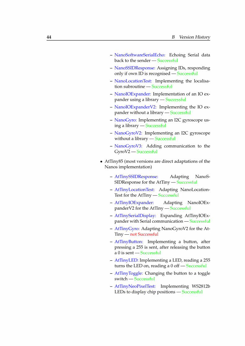
44 B Version History
– NanoSoftwareSerialEcho: Echoing Serial databack to the sender — Successful
– NanoSSIDResponse: Assigning IDs, respondingonly if own ID is recognised — Successful
– NanoLocationTest: Implementing the localisa-tion subroutine — Successful
– NanoIOExpander: Implementation of an IO ex-pander using a library — Successful
– NanoIOExpanderV2: Implementing the IO ex-pander without a library — Successful
– NanoGyro: Implementing an I2C gyroscope us-ing a library — Successful
– NanoGyroV2: Implementing an I2C gyroscopewithout a library — Successful
– NanoGyroV3: Adding communication to theGyroV2 — Successful
• AtTiny85 (most versions are direct adaptations of theNanos implementation)
– AtTinySSIDResponse: Adapting NanoS-SIDResponse for the AtTiny — Successful
– AtTinyLocationTest: Adapting NanoLocation-Test for the AtTiny — Successful
– AtTinyIOExpander: Adapting NanoIOEx-panderV2 for the AtTiny — Successful
– AtTinySerialDisplay: Expanding AtTinyIOEx-pander with Serial communication — Successful
– AtTinyGyro: Adapting NanoGyroV2 for the At-Tiny — not Successful
– AtTinyButton: Implementing a button, afterpressing a 255 is sent, after releasing the buttona 0 is sent — Successful
– AtTinyLED: Implementing a LED, reading a 255turns the LED on, reading a 0 off — Successful
– AtTinyToggle: Changing the button to a toggleswitch — Successful
– AtTinyNeoPixelTest: Implementing WS2812bLEDs to display chip positions — Successful
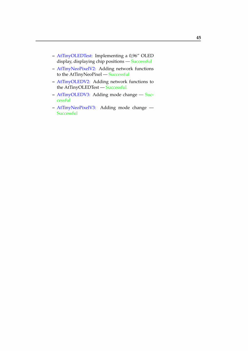
45
– AtTinyOLEDTest: Implementing a 0,96” OLEDdisplay, displaying chip positions — Successful
– AtTinyNeoPixelV2: Adding network functionsto the AtTinyNeoPixel — Successful
– AtTinyOLEDV2: Adding network functions tothe AtTinyOLEDTest — Successful
– AtTinyOLEDV3: Adding mode change — Suc-cessful
– AtTinyNeoPixelV3: Adding mode change —Successful

47
Bibliography
Adafruit. Neopixel, a. URL https://github.com/adafruit/Adafruit_NeoPixel.
Adafruit. Basic connections, b. URL https://learn.adafruit.com/adafruit-neopixel-uberguide/basic-connections.
Adafruit. Tinywirem, c. URL https://github.com/adafruit/TinyWireM.
Anke Brocker, Simon Voelker, Tony Zelun Zhang, MathisMuller, and Jan Borchers. Flowboard: A visual flow-based programming environment for embedded cod-ing. In to appear: Proceedings of the 2019 CHI Conferenceon Human Factors in Computing Systems, CHI ’19, NewYork, NY, USA, May 2019. ACM. ISBN 978-1-4503-5971-9/19/05. doi: 10.1145/3290607.3313247. URL https://doi.org/10.1145/3290607.3313247.
Kinematics. Tinkerbots robotic building kit. URLhttps://www.indiegogo.com/projects/tinkerbots-robotic-building-kit-toys#.
nickstedman. Softwareserialwithhalfduplex.URL https://github.com/nickstedman/SoftwareSerialWithHalfDuplex.
SensorsIot. Tinyozled. URL https://github.com/SensorsIot/TinyOzOled.
SparkFun. qwiic. URL https://www.sparkfun.com/qwiic#connections.
Ryoichi Watanabe, Yuichi Itoh, Michihiro Kawai, Yoshi-fumi Kitamura, Fumio Kishino, and Hideo Kikuchi.
48 Bibliography
Implementation of activecube as an intuitive 3dcomputer interface. In International Symposium onSmart Graphics, pages 43–53. Springer, 2004. URLhttps://link.springer.com/chapter/10.1007/978-3-540-24678-7_5#enumeration.
Jamie Zigelbaum, Michael S Horn, Orit Shaer, andRobert JK Jacob. The tangible video editor: col-laborative video editing with active tokens. InProceedings of the 1st international conference on Tan-gible and embedded interaction, pages 43–46. ACM,2007. URL https://static1.squarespace.com/static/4f57841c24ac1bb6d947d820/t/50f828a6e4b02a75e89d8c95/1358440614743/TangibleVideoEditor_TEI2007.pdf.
Oren Zuckerman. Flowness+ FlowBlocks: uncovering thedynamics of everyday life through playful modeling. PhDthesis, Massachusetts Institute of Technology, 2007. URLhttps://www.media.mit.edu/publications/flowness-flowblocks-uncovering-the-dynamics-of-everyday-life-through-playful-modeling/.

Typeset May 14, 2019