Embed Size (px)
Citation preview
DYNAMIC ENGINEERING 150 DuBois St. Suite C Santa Cruz, CA 95060
831-457-8891 831-457-4793 FAX http://www.dyneng.com
[email protected] Est. 1988
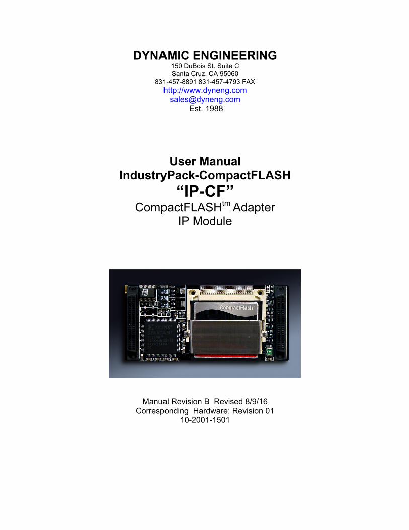
User Manual IndustryPack-CompactFLASH
“IP-CF” CompactFLASHtm Adapter
IP Module
Manual Revision B Revised 8/9/16 Corresponding Hardware: Revision 01
10-2001-1501

E m b e d d e d S o l u t i o n s P g 2 o f 2 0
IP-CF IP Module CompactFLASHTM Adapter
Dynamic Engineering
150 DuBois St. Suite C Santa Cruz, CA 95060
831-457-8891 831-457-4793 FAX www.dyneng.com
This document contains information of proprietary interest to Dynamic Engineering. It has been supplied in confidence and the recipient, by accepting this material, agrees that the subject matter will not be copied or reproduced, in whole or in part, nor its contents revealed in any manner or to any person except to meet the purpose for which it was delivered. Dynamic Engineering has made every effort to ensure that this manual is accurate and complete. Still, the company reserves the right to make improvements or changes in the product described in this document at any time and without notice. Furthermore, Dynamic Engineering assumes no liability arising out of the application or use of the device described herein. The electronic equipment described herein generates, uses, and can radiate radio frequency energy. Operation of this equipment in a residential area is likely to cause radio interference, in which case the user, at his own expense, will be required to take whatever measures may be required to correct the interference. Dynamic Engineering’s products are not authorized for use as critical components in life support devices or systems without the express written approval of the president of Dynamic Engineering. This product has been designed to operate with IP Module carriers and compatible user-provided equipment. Connection of incompatible hardware is likely to cause serious damage. ©2001-2016 by Dynamic Engineering. Other trademarks and registered trademarks are owned by their respective manufactures.
E m b e d d e d S o l u t i o n s P g 3 o f 2 0
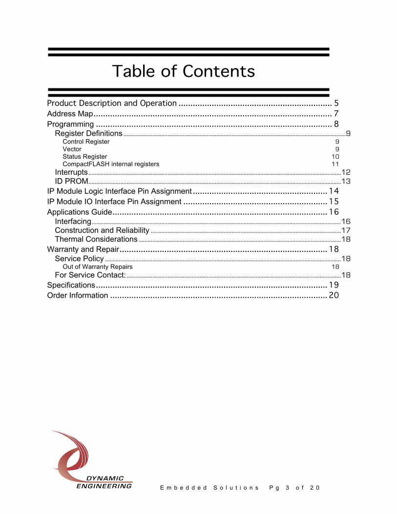
Table of Contents
Product Description and Operation ................................................................. 5Address Map ..................................................................................................... 7Programming .................................................................................................... 8
Register Definitions .................................................................................................................................................. 9Control Register 9Vector 9Status Register 10CompactFLASH internal registers 11
Interrupts ...................................................................................................................................................................... 12ID PROM ...................................................................................................................................................................... 13
IP Module Logic Interface Pin Assignment ......................................................... 14IP Module IO Interface Pin Assignment ............................................................. 15Applications Guide ........................................................................................... 16
Interfacing .................................................................................................................................................................... 16Construction and Reliability ............................................................................................................................. 17Thermal Considerations ..................................................................................................................................... 18
Warranty and Repair ........................................................................................ 18Service Policy ........................................................................................................................................................... 18
Out of Warranty Repairs 18For Service Contact: ............................................................................................................................................. 18
Specifications .................................................................................................. 19Order Information ............................................................................................ 20

E m b e d d e d S o l u t i o n s P g 4 o f 2 0
List of Figures
FIGURE 1 IP-CF ADDRESS MAP 7FIGURE 2 IP-CF CONTROL REGISTER 0 BIT MAP 9FIGURE 3 IP-CF STATUS BIT MAP 10FIGURE 4 IP-CF ID PROM 13FIGURE 5 IP-CF LOGIC INTERFACE 14FIGURE 6 IP-CF IO INTERFACE 15
E m b e d d e d S o l u t i o n s P g 5 o f 2 0
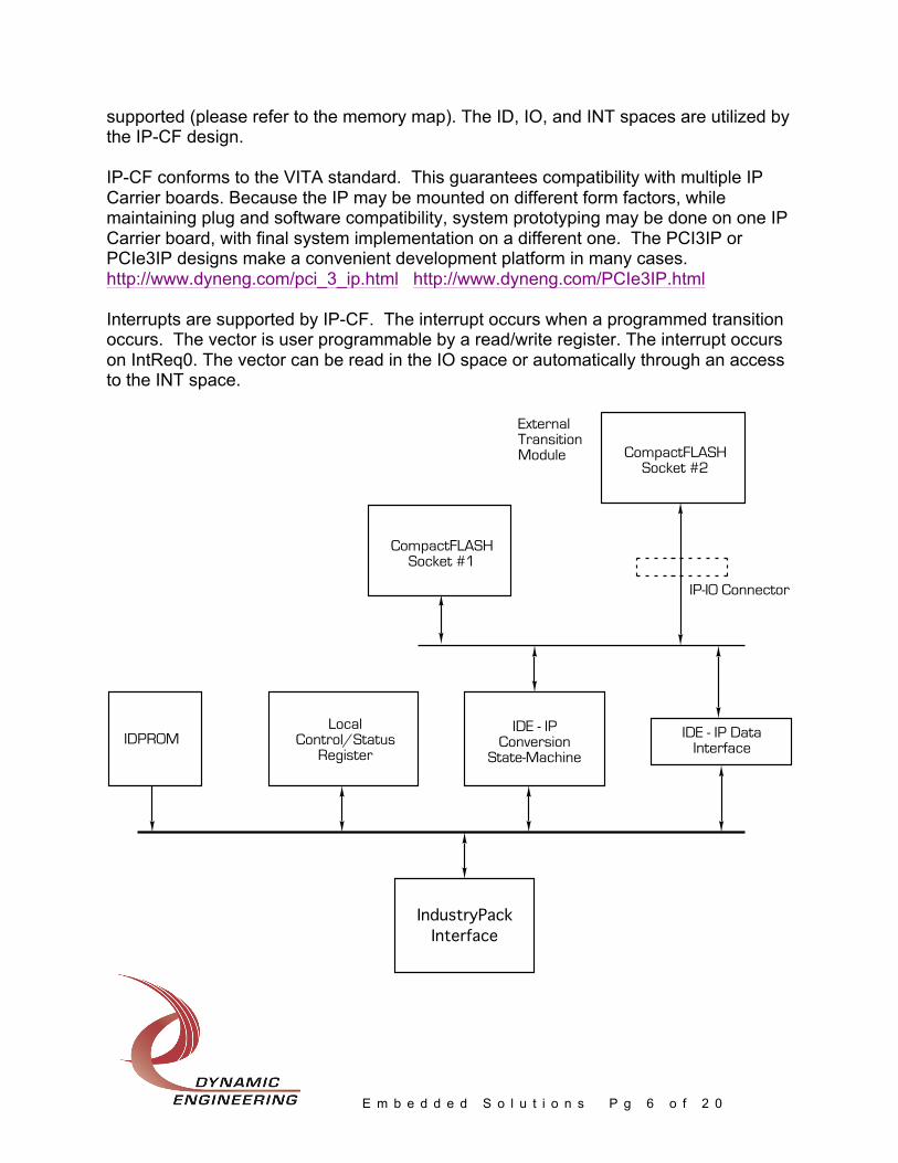
Product Description and Operation IP-CF is part of the IP Module family of modular I/O components. IP-CF is an adapter which converts the IP bus protocol to IDE to allow a CompactFLASH module to be installed into an IP slot. CompactFLASH is available in densities ranging up to GigaBytes. CompactFLASH modules can be communicated with in “true IDE” mode or with a variant specific to CompactFLASH. IP-CF operates in IDE mode to allow other non-CompactFLASH modules to be installed into the adapter. The IP specification limits the height of the components above the IP to prevent interference with the host card. IP-CF meets the type 1 [standard] height requirements and can be used in any slot. A single socket can be placed on the IP Module and meet the requirements. The IDE interface can be expanded to allow two CompactFLASH units to be controlled from one IP-CF. The second unit would be installed on a transition module. The internal unit is set to be the master CompactFLASH device. The selection is done with resistors installed at time of manufacture and can be altered by special request. IP-CF has an oscillator position which is not used for the standard interface. If you have a custom module which requires an alternate timing scheme the oscillator position can be filled to support your requirements. The state-machine has write-through capability to reduce the overhead on the local CPU. The acknowledge signal is asserted when the data is captured within the Xilinx and before the CompactFLASH device is written to. The state-machine completes the data transfer to the CompactFLASH while the local CPU is completing the access and potentially going on to the next set of instructions. If the CPU writes again before the previous transfer is completed the new data is captured and held until the initial write is completed before performing the second write. The acknowledge is held off until the second write is protected to allow an overlapped pipeline to be established between the host and the CompactFLASH with no loss of data. Reads from the CompactFLASH data space are completed with the data fetched from the CompactFLASH without hardware acceleration. We may add a pre-read feature in the future to allow a similar no wait state access for the first read. IP-CF supports both 8 and 32 Mhz. IP Bus operation. All configuration registers support read and write operations for maximum software convenience. Word operations are
E m b e d d e d S o l u t i o n s P g 6 o f 2 0
supported (please refer to the memory map). The ID, IO, and INT spaces are utilized by the IP-CF design. IP-CF conforms to the VITA standard. This guarantees compatibility with multiple IP Carrier boards. Because the IP may be mounted on different form factors, while maintaining plug and software compatibility, system prototyping may be done on one IP Carrier board, with final system implementation on a different one. The PCI3IP or PCIe3IP designs make a convenient development platform in many cases. http://www.dyneng.com/pci_3_ip.html http://www.dyneng.com/PCIe3IP.html Interrupts are supported by IP-CF. The interrupt occurs when a programmed transition occurs. The vector is user programmable by a read/write register. The interrupt occurs on IntReq0. The vector can be read in the IO space or automatically through an access to the INT space.
IndustryPackInterface
IDE - IP Conversion
State-MachineIDPROM
Local Control/Status
Register
IDE - IP Data Interface
CompactFLASH Socket #1
CompactFLASH Socket #2
IP-IO Connector
External Transition Module
E m b e d d e d S o l u t i o n s P g 7 o f 2 0
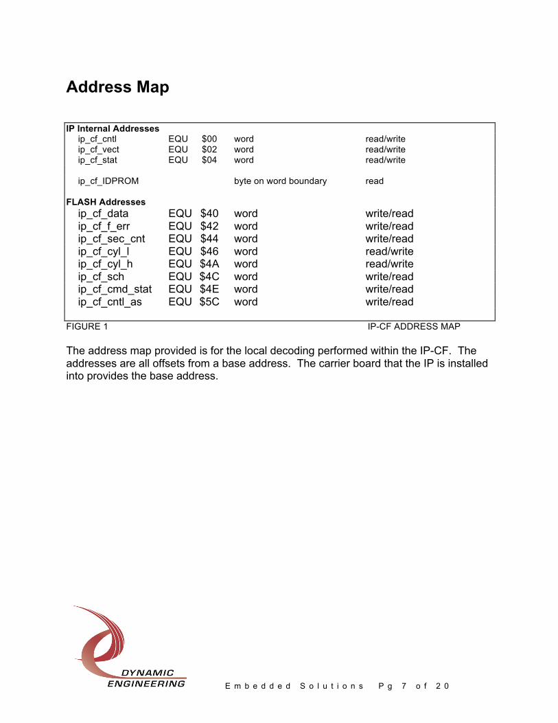
Address Map IP Internal Addresses ip_cf_cntl EQU $00 word read/write ip_cf_vect EQU $02 word read/write ip_cf_stat EQU $04 word read/write ip_cf_IDPROM byte on word boundary read FLASH Addresses ip_cf_data EQU $40 word write/read ip_cf_f_err EQU $42 word write/read ip_cf_sec_cnt EQU $44 word write/read ip_cf_cyl_l EQU $46 word read/write ip_cf_cyl_h EQU $4A word read/write ip_cf_sch EQU $4C word write/read ip_cf_cmd_stat EQU $4E word write/read ip_cf_cntl_as EQU $5C word write/read FIGURE 1 IP-CF ADDRESS MAP The address map provided is for the local decoding performed within the IP-CF. The addresses are all offsets from a base address. The carrier board that the IP is installed into provides the base address.

E m b e d d e d S o l u t i o n s P g 8 o f 2 0
Programming Programming IP-CF requires only the ability to read and write data in the host’s I/O space. The base address is determined by the IP Carrier board. Please refer to the CompactFLASH programmers manual for detailed bit-map information and other programming details. The manual is available from the manufacturers website. Dynamic Engineering currently uses Sandisk CompactFLASH modules. The IP acts as a bridge between the IP bus interface and the CompactFLASH module. There are a few settings to insure proper operation. This manual covers the internal registers of the IP-CF. Most of the operational interface is controlled by the CompactFLASH module and is covered by the CompactFLASH Manual. The engineering kit provides reference software which Dynamic Engineering uses to test the IP-CF. The IP-CF is mounted to a PCI3IP carrier. [ http://www.dyneng.com/pci_3_ip.html ] Windows 7 is the OS. The Identify Disk information is read and checked. The model, serial number and firmware revision are displayed. The IDPROM is read and checked. The vector register has a loop-back test. The FLASH memory is programmed and read-back. The read-write test to the FLASH finds the first non-programmed sector, programs that sector and then reads the data back. If the test is looped the data is read many times and only programmed once. If the software is re-launched then the next sector will be written to and then read back. We do the sector marking to keep from doing excessive writes in test. The CompactFLASH interrupts and control functions are tested during the identify and r/w tests. The source code for the application is included for your reference. In addition to the software, the engineering kit includes a reference schematic plus the IP-Debug-Bus and the IP-Debug-IO. Linux and VxWorks drivers will be available soon. If you need a custom version of the card or a custom driver please contact Dynamic Engineering. Please note that some carrier boards do not use the interrupt vector. Some carriers require the interrupt vector. If needed, the vector register and the interrupt service routine should be loaded and the mask set.
E m b e d d e d S o l u t i o n s P g 9 o f 2 0
Register Definitions
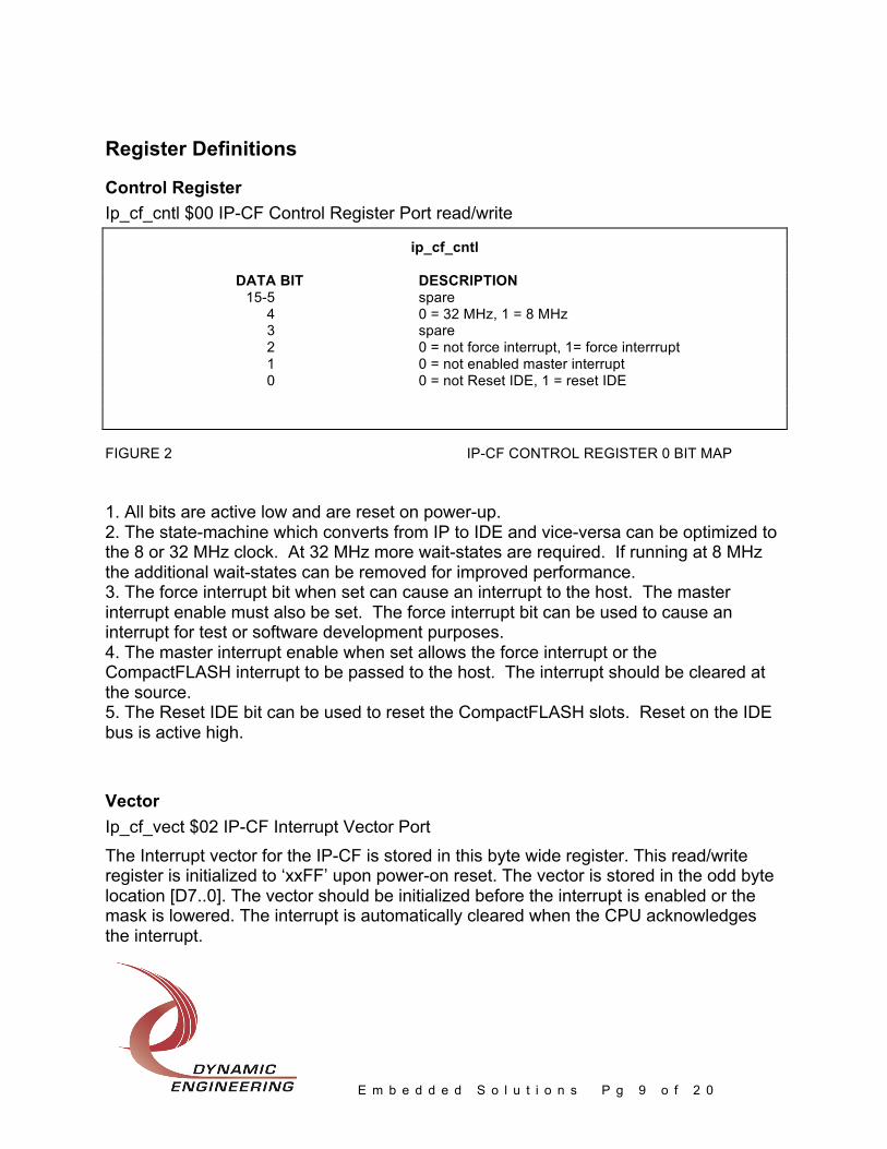
Control Register Ip_cf_cntl $00 IP-CF Control Register Port read/write
ip_cf_cntl
DATA BIT DESCRIPTION 15-5 spare 4 0 = 32 MHz, 1 = 8 MHz 3 spare 2 0 = not force interrupt, 1= force interrrupt 1 0 = not enabled master interrupt 0 0 = not Reset IDE, 1 = reset IDE
FIGURE 2 IP-CF CONTROL REGISTER 0 BIT MAP 1. All bits are active low and are reset on power-up. 2. The state-machine which converts from IP to IDE and vice-versa can be optimized to the 8 or 32 MHz clock. At 32 MHz more wait-states are required. If running at 8 MHz the additional wait-states can be removed for improved performance. 3. The force interrupt bit when set can cause an interrupt to the host. The master interrupt enable must also be set. The force interrupt bit can be used to cause an interrupt for test or software development purposes. 4. The master interrupt enable when set allows the force interrupt or the CompactFLASH interrupt to be passed to the host. The interrupt should be cleared at the source. 5. The Reset IDE bit can be used to reset the CompactFLASH slots. Reset on the IDE bus is active high. Vector Ip_cf_vect $02 IP-CF Interrupt Vector Port The Interrupt vector for the IP-CF is stored in this byte wide register. This read/write register is initialized to ‘xxFF’ upon power-on reset. The vector is stored in the odd byte location [D7..0]. The vector should be initialized before the interrupt is enabled or the mask is lowered. The interrupt is automatically cleared when the CPU acknowledges the interrupt.
E m b e d d e d S o l u t i o n s P g 1 0 o f 2 0
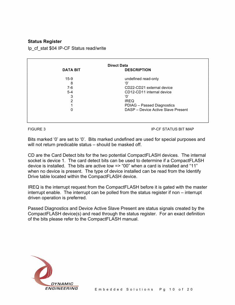
Status Register Ip_cf_stat $04 IP-CF Status read/write
Direct Data DATA BIT DESCRIPTION 15-9 undefined read-only 8 ‘0’ 7-6 CD22-CD21 external device 5-4 CD12-CD11 internal device 3 ‘0’ 2 IREQ 1 PDIAG – Passed Diagnostics 0 DASP – Device Active Slave Present
FIGURE 3 IP-CF STATUS BIT MAP Bits marked ‘0’ are set to ‘0’. Bits marked undefined are used for special purposes and will not return predicable status – should be masked off. CD are the Card Detect bits for the two potential CompactFLASH devices. The internal socket is device 1. The card detect bits can be used to determine if a CompactFLASH device is installed. The bits are active low => “00” when a card is installed and “11” when no device is present. The type of device installed can be read from the Identify Drive table located within the CompactFLASH device. IREQ is the interrupt request from the CompactFLASH before it is gated with the master interrupt enable. The interrupt can be polled from the status register if non – interrupt driven operation is preferred. Passed Diagnostics and Device Active Slave Present are status signals created by the CompactFLASH device(s) and read through the status register. For an exact definition of the bits please refer to the CompactFLASH manual.

E m b e d d e d S o l u t i o n s P g 1 1 o f 2 0
CompactFLASH internal registers ip_cf_data 0x40 // compact flash read/write data pointer ip_cf_f_err 0x42 // compact flash write feature/read error ip_cf_sec_cnt 0x44 // compact flash read/write sector count pointer ip_cf_sec_num 0x46 // compact flash read/write sector number pointer iip_cf_cyl_l 0x48 // compact flash read/write cylinder number low pointer ip_cf_cyl_h 0x4a // compact flash read/write cylinder number high pointer ip_cf_sch 0x4c // compact flash read/write select card, head pointer ip_cf_cmd_stat 0x4e // compact flash write command/read status pointer ip_cf_cntl_as 0x5c // compact flash write control/read alt status pointer Please refer to the CompactFLASH manuals for bit-map information.

E m b e d d e d S o l u t i o n s P g 1 2 o f 2 0
Interrupts All IP Module interrupts are vectored. The vector from IP-CF comes from a vector register loaded as part of the initialization process. The vector register can be programmed to any 8 bit value. The default value is $FF which is sometimes not a valid user vector. The software is responsible for choosing a valid user vector. The CompactFLASH state machines generate an interrupt request when a programmed condition is detected. The interrupt is mapped to interrupt request 0. The CPU may respond by asserting INT. The hardware will automatically supply the appropriate interrupt vector when accessed by the CPU. The source of the interrupt is obtained by reading the CompactFLASH internal registers. Some carrier boards pre-fetch data. If your carrier board pre-fetches the interrupt status, then the status may be cleared when the SW goes to look at it. If this is an issue then be careful with the order of reading the registers to prevent the pre-fetching function from affecting operation. The interrupt level seen by the CPU is determined by the IP Carrier board being used. The master interrupt can be disabled or enabled through the ip_cf_cntl register. The Interrupt acknowledge cycle fetches the vector, but does not clear the interrupt request in this design. The interrupt acknowledge cycle is not needed for this design and is supported to be in compliance with the IP Module standard. If your design does not need to use the interrupt vector then the Interrupt space and vector can be bi-passed in favor of direct access to the CompactFLASH module for interrupt status information. If operating in a polled mode and making use of the interrupts for status then the master interrupt should be disabled.

E m b e d d e d S o l u t i o n s P g 1 3 o f 2 0
ID PROM Every IP contains an ID PROM, whose size is at least 32 x 8 bits. The ID PROM aids in software auto configuration and configuration management. The user’s software, or a supplied driver, may verify that the device it expects is actually installed at the location it expects, and is nominally functional. The ID PROM contains the manufacturing revision level of the IP. If a driver requires that a particular revision to be present, it may check for it directly. The location of the ID PROM in the host’s address space is dependent on which carrier is used. Standard data in the ID PROM on the IP-CF is shown in the figure below. For more information on IP ID PROMs refer to the IP Module Logic Interface Specification, available from Dynamic Engineering. Each of the modifications to the IP-CF board will be recorded with a new code in the DRIVER ID and reserved fields. Address Data IP-CF 01 ASCII “I” $49 03 ASCII “P” $50 05 ASCII “A” $41 07 ASCII “H” $48 09 Manufacturer ID $1E 0B Model Number $05 0D Revision $A0 0F reserved $00 11 Driver ID, low byte $00 13 Driver ID, high byte $00 15 No of extra bytes used $0C 17 CRC $4D
FIGURE 4 IP-CF ID PROM

E m b e d d e d S o l u t i o n s P g 1 4 o f 2 0
IP Module Logic Interface Pin Assignment The figure below gives the pin assignments for the IP Module Logic Interface on the IP-CF. Pins marked n/c below are defined by the specification, but not used on the IP-CF. Also see the User Manual for your carrier board for more information. GND GND 1 26
CLK +5V 2 27 Reset* R/W* 3 28 D0 IDSEL* 4 29 D1 DMAReq0* 5 30 D2 MEMSEL* 6 31 D3 DMAReq1* 7 32 D4 IntSel* 8 33 D5 DMAck* 9 34 D6 IOSel* 10 35 D7 n/c 11 36 D8 A1 12 37 D9 DMAEnd* 13 38 D10 A2 14 39 D11 n/c 15 40 D12 A3 16 41 D13 IntReq0* 17 42 D14 A4 18 43 D15 IntReq1* 19 44 BS0* A5 20 45 BS1* n/c 21 46 n/c A6 22 47 n/c Ack* 23 48 +5V n/c 24 49 GND GND 25 50 NOTE 1: The no-connect signals above are defined by the IP Module Logic Interface Specification, but not used by this IP. See the Specification for more information. NOTE 2: The layout of the pin numbers in this table corresponds to the physical placement of pins on the IP connector. Thus this table may be used to easily locate the physical pin corresponding to a desired signal. Pin 1 is marked with a square pad on the IP Module.
FIGURE 5 IP-CF LOGIC INTERFACE
E m b e d d e d S o l u t i o n s P g 1 5 o f 2 0
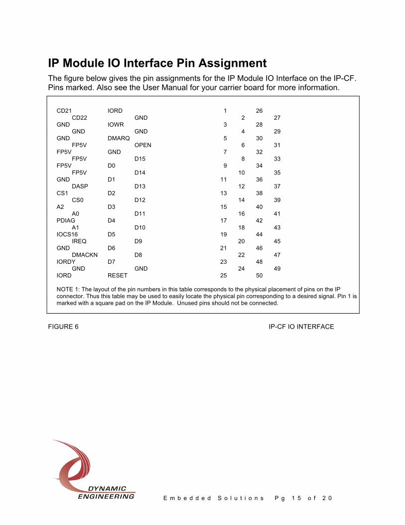
IP Module IO Interface Pin Assignment The figure below gives the pin assignments for the IP Module IO Interface on the IP-CF. Pins marked. Also see the User Manual for your carrier board for more information.
CD21 IORD 1 26
CD22 GND 2 27 GND IOWR 3 28 GND GND 4 29 GND DMARQ 5 30 FP5V OPEN 6 31 FP5V GND 7 32 FP5V D15 8 33 FP5V D0 9 34 FP5V D14 10 35 GND D1 11 36 DASP D13 12 37 CS1 D2 13 38 CS0 D12 14 39 A2 D3 15 40 A0 D11 16 41 PDIAG D4 17 42 A1 D10 18 43 IOCS16 D5 19 44 IREQ D9 20 45 GND D6 21 46 DMACKN D8 22 47 IORDY D7 23 48 GND GND 24 49 IORD RESET 25 50 NOTE 1: The layout of the pin numbers in this table corresponds to the physical placement of pins on the IP connector. Thus this table may be used to easily locate the physical pin corresponding to a desired signal. Pin 1 is marked with a square pad on the IP Module. Unused pins should not be connected.
FIGURE 6 IP-CF IO INTERFACE

E m b e d d e d S o l u t i o n s P g 1 6 o f 2 0
Applications Guide Interfacing Some general interfacing guidelines are presented below. Do not hesitate to contact the factory if you need more assistance. Watch the system grounds. All electrically connected equipment should have a fail safe common ground that is large enough to handle all current loads without affecting noise immunity. Power supplies and power consuming loads should all have their own ground wires back to a common point. Power all system power supplies from one switch. Connecting external voltage to the IP-CF when it is not powered can damage it, as well as the rest of the host system. This problem may be avoided by turning all power supplies on and off at the same time. We provide the components. You provide the system. Safety and reliability can be achieved only by careful planning and practice. Inputs can be damaged by static discharge, by applying voltage less than ground or more than +5 volts with the IP powered. With the IP unpowered, driven input voltages should be kept within .7 volts of ground potential. Terminal Block. We offer a high quality 50 screw terminal block that directly connects to the flat cable. The terminal block mounts on standard DIN rails. [ http://www.dyneng.com/HDRterm50.html ] Many flat cable interface products are available from third party vendors to assist you in your system integration and debugging. These include connectors, cables, test points, ‘Y’s, 50 pin in-line switches, breakout boxes, etc.

E m b e d d e d S o l u t i o n s P g 1 7 o f 2 0
Construction and Reliability IP Modules were conceived and engineered for rugged industrial environments. The IP-CF is constructed out of 0.062 inch thick high temp FR4 material. Through hole and surface mounting of components are used. IC sockets use high quality plated screw machine pins. High insertion and removal forces are required, which assists in the retention of components. If the application requires unusually high reliability or is in an environment subject to high vibration, the user may solder the corner pins of each socketed IC into the socket, using a grounded soldering iron. The IP Module connectors are keyed and shrouded with Gold plated pins on both plugs and receptacles. They are rated at 1 Amp per pin, 200 insertion cycles minimum. These connectors make consistent, correct insertion easy and reliable. The IP is secured against the carrier with four metric M2 stainless steel screws. The heads of the screws are countersunk into the IP. The four screws provide significant protection against shock, vibration, and incomplete insertion. For most applications, they are not required. Please order standard mounting kit for IPs if you want this option. [IP-MTG-KIT]
The IP Module provides a low temperature coefficient of 0.89 W/oC for uniform heat. This is based upon the temperature coefficient of the base FR4 material of 0.31 W/m-oC, and taking into account the thickness and area of the IP. The coefficient means that if 0.89 Watts are applied uniformly on the component side, then the temperature difference between the component side and solder side is one degree Celsius.
E m b e d d e d S o l u t i o n s P g 1 8 o f 2 0
Thermal Considerations The IP-CF design consists of CMOS circuits. The power dissipation due to internal circuitry is very low. It is possible to create a higher power dissipation with the externally connected logic. If more than one a Watt is required to be dissipated due to external loading then forced air cooling is recommended. With the one degree differential temperature to the solder side of the board external cooling is easily accomplished.
Warranty and Repair Please refer to the warranty page for the current warranty offered and options. http://www.dyneng.com/warranty.html
Service Policy Before returning a product for repair, verify as well as possible that the suspected unit is at fault. Then call the Customer Service Department for a RETURN MATERIAL AUTHORIZATION (RMA) number. Carefully package the unit, in the original shipping carton if this is available, and ship prepaid and insured with the RMA number clearly written on the outside of the package. Include a return address and the telephone number of a technical contact. For out-of-warranty repairs, a purchase order for repair charges must accompany the return. Dynamic Engineering will not be responsible for damages due to improper packaging of returned items. For service on Dynamic Engineering Products not purchased directly from Dynamic Engineering contact your reseller. Products returned to Dynamic Engineering for repair by other than the original customer will be treated as out-of-warranty. Out of Warranty Repairs Out of warranty repairs will be billed on a material and labor basis. Customer approval will be obtained before repairing any item if the repair charges will exceed one half of the quantity one list price for that unit. Return transportation and insurance will be billed as part of the repair and is in addition to the minimum charge.
For Service Contact: Customer Service Department Dynamic Engineering 150 DuBois St Suite C Santa Cruz, CA 95060 831-457-8891 831-457-4793 fax Internet Address [email protected]
E m b e d d e d S o l u t i o n s P g 1 9 o f 2 0
Specifications Logic Interface: IP Module Logic Interface
CompactFLASH: One CompactFLASH compatible socket provided. External transition module
can be used to add a second module.
Software Interface: Control Registers, ID PROM, Vector Register, Status Ports
Initialization: Hardware Reset forces all registers to 0.
Access Modes: Word I/O Space (see memory map) Word in ID Space Vectored interrupt
Access Time: Access time depends on CompactFLASH Module. back-to-back cycles in 500ns (8Mhz.) or 125 nS (32 Mhz.) for internal operations. Approximately 1 uS for CompactFLASH accesses. Write operations are posted and return for pipelined operation. Read accesses are data delayed.
Interrupt: Masked or polled operation. Master interrupt enable and status. INTRQ0 only.
DMA: No Logic Interface DMA Support implemented at this time. Onboard Options: All Options are Software Programmable
Interface Options: 50 pin flat cable
50 screw terminal block interface [HDRterm50] User cable none required.
Dimensions: Standard Single IP Module. 1.8 x 3.9 x 0.344 (max.) inches
Construction: FR4 Multi-Layer Printed Circuit, Through Hole and Surface Mount Components. Programmable parts are socketed.
Temperature Coefficient: 0.89 W/oC for uniform heat across IP
Power: Max. TBD mA @ 5

E m b e d d e d S o l u t i o n s P g 2 0 o f 2 0
Order Information IP-CF board has 9 standard configurations. http://www.dyneng.com/ip_cf.html
“no dash” IP Module with 256 Mb of CompactFLASH
“-10” IP Module with 1 Gb of CompactFLASH
“-11” IP Module with 2 Gb of CompactFLASH Tools for IP-CF IP-Debug-Bus - IP Bus interface extender with testpoints,
isolated power and quickswitch technology to allow hot swapping of IPs or power cycling without powering down the host. http://www.dyneng.com/ipdbgbus.html
PCIe3IP 1/2 length PCIe card with 3 IP slots. http://www.dyneng.com/PCIe3IP.html
PCI3IP 1/2 length PCI card with 3 IP slots. http://www.dyneng.com/pci_3_ip.html
IP-MTG-KIT – 4 metric stainless screw and stand-off pairs to retain IP-CF against the carrier board. Flat head screws match IP Specification mounting requirements.
All information provided is Copyright Dynamic Engineering