Embed Size (px)
Citation preview

PCcardsDirect
PCcardsDirect.comIndustrial Flash Spcifications
P.1
PCcardsDirect PC Flash
Industrial CompactFlash Card
Product Specification
V 3 . 0

PCcardsDirect
PCcardsDirect.com Industrial CompactFlash Card
P.2
Contents: 1. Scope...........................................................................................................................3 2. Introduction.................................................................................................................3 3. System Features .........................................................................................................3 4. Product Specifications ...............................................................................................4
4.1. System Environmental Specification..........................................................4 4.2. System Power Requirement ........................................................................4 4.3. System Performance....................................................................................4 4.4. System Reliability.........................................................................................4 4.5. Physical Specifications................................................................................5 4.6. Capacity Specification .................................................................................6
5. Interface Description ..................................................................................................7 5.1. Pin Assignments ..........................................................................................7 5.2. Signals’ Identification...................................................................................8 5.3. Pin Descriptions ...........................................................................................9 5.4. CompactFlash I/O Mapping Address ........................................................13 5.5. Card Block Diagram ...................................................................................14
6. Electrical Specification ............................................................................................14 6.1. Power Pin Description ...............................................................................14 6.2. Absolute Maximum Rating ........................................................................14 6.3. Input Power.................................................................................................15 6.4. Input Leakage Current ...............................................................................15 6.5. Input Characteristics..................................................................................15 6.6. Output Drive Type.......................................................................................15 6.7. Output Drive Characteristics.....................................................................16 6.8. DC Characteristics .....................................................................................16 6.9. AC Characteristics .....................................................................................17 6.10. CompactFlash Card Registers and Memory Space Decoding................23 6.11. I/O Primary and Secondary Address Configurations ..............................27 6.12. Power Management....................................................................................29
7. CF – ATA Command Description .............................................................................30 7.1. CF – ATA Command Set .............................................................................31
A. Order Information ..............................................................................................42 1. Part Number .......................................................................................................42 2. Part Number Decoder........................................................................................42

PCcardsDirect
PCcardsDirect.com Industrial CompactFlash Card
P.3
1. Scope This document describes the features and specifications and installation guide of PCcardsDirect's Industrial CompactFlash Card products. In the appendix, there provides order information, and warranty policy.
2. Introduction PCcardsDirect's Industrial CompactFlash Cards combine advanced Flash controller technology and NAND Type SLC flash memory. The PCcardsDirect's Industrial CompactFlash Card includes industrial operating temperature grade of (-40ºC ~+85ºC) to fulfill various specialized applications innormal or harsh operating environments. PCcardsDirect's Industrial CompactFlash™ Card is the ideal solution for critical applications operating in harsh enviormental conditions.
3. System Features CompactFlash specification: PCMCIA ver.2.1 and PC Card ATA ver.2.01 compatible
- 50pin SMT connector and type I 3 variations of access mode
Memory Card Mode I/O Card Mode.
True-IDE Mode Very low power consumption Very high performance Rugged environment is working well Automatic error correction and retry capabilities Supports power down commands and Auto Stand-by / Sleep Mode Low weight Noiseless MTBF > 1,000,000 hours Minimum 10,000 insertions Support O/S: Windows 31/95/98/Me, Windows NT/2000/XP/2003, WinCE, QNX, Linux,
DOS and more Capacity: 16MB, 32MB, 64MB,128MB, 256MB, 512 MB, 1GB, 2GB,4GB,
8GB.(unformatted)
PCcardsDirect
PCcardsDirect
PCcardsDirect.com Industrial CompactFlash Card
P.4
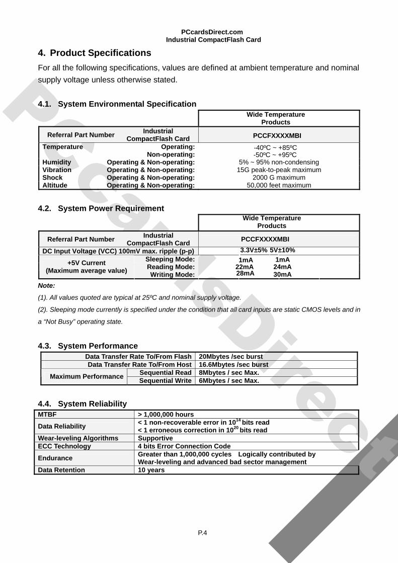
4. Product Specifications For all the following specifications, values are defined at ambient temperature and nominal supply voltage unless otherwise stated. 4.1. System Environmental Specification
Wide Temperature Products
Referral Part Number Industrial CompactFlash Card PCCFXXXXMBI
Temperature Operating:Non-operating:
-40ºC ~ +85ºC -50ºC ~ +95ºC
Humidity Operating & Non-operating: 5% ~ 95% non-condensing Vibration Operating & Non-operating: 15G peak-to-peak maximum Shock Operating & Non-operating: 2000 G maximum Altitude Operating & Non-operating: 50,000 feet maximum
4.2. System Power Requirement
Wide Temperature Products
Referral Part Number Industrial CompactFlash Card PCCFXXXXMBI
DC Input Voltage (VCC) 100mV max. ripple (p-p) 3.3V±5% 5V±10% Sleeping Mode: 1mA 1mA Reading Mode: 22mA 24mA +5V Current
(Maximum average value) Writing Mode: 28mA 30mA Note:
(1). All values quoted are typical at 25ºC and nominal supply voltage.
(2). Sleeping mode currently is specified under the condition that all card inputs are static CMOS levels and in
a “Not Busy” operating state.
4.3. System Performance Data Transfer Rate To/From Flash 20Mbytes /sec burst Data Transfer Rate To/From Host 16.6Mbytes /sec burst
Sequential Read 8Mbytes / sec Max. Maximum Performance Sequential Write 6Mbytes / sec Max. 4.4. System Reliability MTBF > 1,000,000 hours
Data Reliability < 1 non-recoverable error in 1014 bits read < 1 erroneous correction in 1020 bits read
Wear-leveling Algorithms Supportive ECC Technology 4 bits Error Connection Code
Endurance Greater than 1,000,000 cycles Logically contributed by Wear-leveling and advanced bad sector management
Data Retention 10 years

PC PCcardsDirect.com
Industrial CompactFlash Card 4.5. Physical Specifications 4.5.1. Physical Specifications
Industrial CompactFlash Card Length: 36.40 ± 0.15 mm (1.433 ±.006 in)
Width: 42.80 ± 0.10 mm (1.685 ±.004 in) Thickness: 3.3 mm ± 0.10 mm (.130 ±.004 in) (Excluding Lip)
Weight: 11.4 g (.40 oz) typical, 14.2 g (.50 oz) maximum
4.5.2. Dimension - Unit: mm [inch]
cardsDirectP.5

PCcardsDirect
PCcardsDirect.com Industrial CompactFlash Card
P.6
4.6. Capacity Specification 4.6.1. The Card Configurations
Disk Capacity ........PCcardsDirectPCFLASH Part Number Matrix
32MB Removable Disk ID:
64MB
128MB
256MB
512MB
1GB
2GB
4GB
4.6.2. The specific capacity for the various models and the default number of heads, sectors/track and cylinders.
Unformatted
Capacity
Default
Cylinder
Default
Head
Default
Sector
Defaulted CHS
Capacity
16MB 248 04 32 16,252,928
32MB 496 04 32 32,505,856
64MB 978 04 32 64,094,208
128MB 978 8 32 128,188,416
256MB 978 16 32 256,376,832
512MB 993 16 63 512,483,328
1,024MB 1,985 16 63 1,024,450,560
2.04GB 3,954 16 63 2,040,643,584
4GB 7,889 16 63 4,071,481,344
Removable Disk ID:
Removable Disk ID:
Removable Disk ID:
Removable Disk ID:
Removable Disk ID:
Removable Disk ID:
Removable Disk ID:
PCCF32MBI
PCCF64MBI
PCCF128MBI
PCCF256MBI
PCCF512BI
PCCF1024MBI
PCCF2048MBI
PCCF4096MBI

PCcardsDirect
5. Interface Description 5.1. Pin Assignments
Memory card mode I/O card mode True IDE mode
Pin NO. Signal name I/O Signal name I/O Signal name I/O
1 GND - GND - GND -
2 D3 I/O D3 I/O D3 I/O
3 D4 I/O D4 I/O D4 I/O
4 D5 I/O D5 I/O D5 I/O
5 D6 I/O D6 I/O D6 I/O
6 D7 I/O D7 I/O D7 I/O
7 -CE1 | -CE1 | -CE1 |
8 A10 | A10 | A10 |
9 -OE | -OE | -ATASEL |
10 A9 | A9 | A9 |
11 A8 | A8 | A8 |
12 A7 | A7 | A7 |
13 VCC - VCC - VCC -
14 A6 | A6 | A6 |
15 A5 | A5 | A5 |
16 A4 | A4 | A4 |
17 A3 | A3 | A3 |
18 A2 | A2 | A2 |
19 A1 | A1 | A1 |
20 A0 | A0 | A0 |
21 D0 I/O D0 I/O D0 I/O
22 D1 I/O D1 I/O D1 I/O
23 D2 I/O D2 I/O D2 I/O
24 WP O -IOIS16 O -IOIS16 O
25 -CD2 O -CD2 O -CD2 O
26 -CD1 O -CD1 O -CD1 O
27 D11 I/O D11 I/O D11 I/O
28 D12 I/O D12 I/O D12 I/O
29 D13 I/O D13 I/O D13 I/O
30 D14 I/O D14 I/O D14 I/O
31 D15 I/O D15 I/O D15 I/O
32 -CE2 | -CE2 | -CE2 | PP
PCcardsDirect.com Industrial CompactFlash Card
P. 7

PCcardsDirect
3 -VS1 O -VS1 O -VS1 O
34 -IORD | -IORD | -IORD |
35 -IOWR | -IOWR | -IOWR |
36 -WE | -WE | -WE |
37 RDY/-BSY O -IREQ O INTRQ O
38 VCC — VCC — VCC —
39 -CSEL | -CSEL | -CSEL |
40 -VS2 O -VS2 O -VS2 O
41 RESET | RESET | -RESET |
42 -WAIT O -WAIT O IORDY O
43 -INPACK O -INPACK O -INPACK O
44 -REG | -REG | -REG |
45 BVD2 I/O -SPKR I/O -DASP I/O
46 BVD1 I/O -STSCHG I/O -PDIAG I/O
47 D8 I/O D8 I/O D8 I/O
48 D9 I/O D9 I/O D9 I/O
49 D10 I/O D10 I/O D10 I/O
50 GND — GND — GND —
5.2. Signals’ Identification
Symbol Function
D0 ~ D15 Data Bus (Bi-directional)
A0 ~ A10 Address Bus (Input)
/CE1,/CE2 Card Enable (Input)
/OE, /WE Output / Write Enable (Input)
/REG Register Select (Input)
/IORD, /IOWR I/O Access (Input)
/IREQ, /IOIS16,
RESET, CSEL, I/O Handshaking (Input/Output)
/INPACK, /WAIT, DASP, PDIAG VSS Ground
VCC Vcc Power Input
PCcardsDirect.com Industrial CompactFlash Card
P.8

PCcardsDirect
Pin Descriptions Signal Name Dir Pin No. Description
A10 to A0
(PC Card Memory
Mode)
A10 to A0
(PC Card I/O Mode)
8,10,11,12,14,15,16,17,18,19,20
These address lines along with the-REG signal are
used to select the following: The I/O port address
registers within the CompactFlash Storage Card or
CF + Card, the memory mapped port add address
registers within the CompactFlash Storage Card or
CF+ Card , a byte in the card’s information
structure and its configuration control and status
registers.
A2 to A0
(True IDE Mode)
I
18,19,20
In True IDE Mode only {2:0} are used to select the one of eight registers in the Task File. The remaining address lines should be grounded by the host.
BVD1 (PC Card Memory Mode)
This signal is asserted high as BVD1 is not supported.
-STSCHG (PC Card Memory Mode)
This Signal is asserted low to alert the host to changes in the RDY/-BSY and Write Protect states; while the I/O interface is configured. Its use is controlled by the Card Configured and Status Register.
-PDIAG (True IDE Mode)
I/O 46
In the True IDE Mode, this input/output is the Pass Diagnostic signal in the Master/Slave handshake protocol.
BVD2 (PC Card Memory Mode)
This signal is asserted high, as BVD2 is not supported.
-SPKR (PC Card I/O Mode)
This line is Binary AUDIO OUTPUT From the Card. If the Card doesn’t support the Binary Audio function, this line should be held negated.
-DASP (True IDE Mode)
I/O 45
In the True IDE Mode, this input/output is the Disk Active/Slave Present signal in the Master/Slave.
-CD1, -CD2 (PC Card Memory Mode)
O 25,26
These Card Detect pins are connected to ground on the CompactFlash Storage Card or CF+ Card. They are used by the host to determined that the CompactFlash Storage Card or CF+ Card is fully inserted into its socket.
-CE1,-CE2 (PC Card Memory Mode)
-CE1,-CE2 (PC Card I/O Mode)
I 7,32 There input signals are used both to select the card and to indicate to the card whether a byte or a word operation is being performed. –CE2 always accesses the odd byte of the word depending on A0 and –CE2. A multiplexing scheme based on A1. –DE1,
PCcardsDirect.com Industrial CompactFlash Card
P. 9

PCcardsDirect
CE2 allow 8-bit hosts to access all data on D0 to D7. See Access Specification below.
-CS0,-CS1 (True IDE Mode)
In the True IDE Mode CS0 is the chip select for the task file registers while CS1 is used to select the Alternate Status Register and Device Control Register.
-CSEL (PC Card Memory Mode)
This signal is not used for this mode.
-CSEL (PC Card I/O Mode)
-CSEL (True IDE Mode)
I 39 This internally pulled up signal is used to configure this device as a Master or a Slave when configured in the True IDE Mode. When this pin is grounded, this device is configured as a Master. When the pin is open, this device is configured as a Slave.
D15 to D00 (PC Card Memory Mode) D15 to D00 (PC Card I/O Mode)
These lines carry the Data, commands and Status information between the host and the controller. D00 is the LSB of the Even Byte of the Word D08 is the LSB of the Odd Byte of the Word.
D15 to D00 (True IDE Mode)
I/O31,30,29,38,37,49,48,48,6,5,4,
3,2,23,22,21 True IDE Mode, all Task File operations occur in byte mode on the low order bus D00 to D07 while all data transfers are 16 but using D00 to D15.
GND (PC Card Memory Mode) GND (PC Card I/O Mode) GND (True IDE Mode)
- 1,50 Ground
-INPCAK (PC Card Memory Mode)
This signal is not used in this Mode.
-INPACK (PC Card I/O Mode)
The Input Acknowledge signal is asserted by the CompactFlash Storage Card or CF+ Card when the card is selected and responding to an I/O read cycle at the address that is on the address bus. This signal is used by the host to control the enable of any input data buffers between the CompactFlash Storage Card or CF+ Card and the CPU.
-INPACK (True IDE Mode)
O 43
In True IDE Mode this output signal is not used and should not be connected at the host.
-IORD (PC Card Memory Mode)
I 34 This signal is not used in this mode.
PCcardsDirect.com Industrial CompactFlash Card
P.10

PCcardsDirect
ORD (PC Card I/O Mode)
This is an I/O Read strobe generated by the host. This signal gates I/O data onto the bus from the CompactFlash Storage Card or CF+ Card when the card is configured to use the I/O interface.
-IORD (True IDE Mode)
In True IDE Mode, this signal has same function as in PC Card I/O Mode.
-IOWR (PC Card Memory Mode)
This signal is not used in this mode.
-IOWR (PC Card I/O Mode)
The I/O Write strobe pulse is used to clock I/O data on the Card Data bus into the CompactFlash Storage Card or CF+ Card controller registers when he Compact Storage Card or CF+ Card is configured to use the I/O interface. The clocking will occur on the negative to positive edge of the signal (Trailing edge).
-IOWR (True IDE Mode)
I 35
In True IDE Mode, this signal has the same function as in PC Card I/O Mode.
-OE (PC Card Memory Mode)
This is an Output Enable strobe generated by the host interface. It is used to read data from the CompactFlash Storage Card or CF+ Card in Memory Mode and to read the CIS and configuration registers.
-OE (PC Card I/O Mode)
In PC Card I/O Mode. This signal is used to read the CIS and configuration registers.
-ATA SEL (True IDE Mode)
I 9
To enable True IDE Mode this input should be grounded by the host.
PDY/BSY (PC Card Memory Mode)
In Memory Mode this signal is set high when the CompactFlash Storage Card or CF+ Card is ready to accept a new data transfer operation and held low when the card is busy. Theo Host memory card socket must provide a pull-up resistor. At power up and at Reset the RDY/-BSY signal is held low (busy) until the CompactFlash Storage Card or CF+ Card has completed its power up or reset function. No access of any type should be made to the CompactFlash Storage Card or CF+ Card during this time. The RDY/-BSY signal is held high (disabled from being busy) whenever the following condition is true. The CompactFlash Storage Card or CF+ Card has been powered up with + RESET continuously disconnected or asserted.
-IREQ (PC Card I/O Mode)
O 37
Operation – After the CompactFlash Storage Card or CF+ Card has been configured for I/O operational this signal is used as interrupt
PCcardsDirect.com Industrial CompactFlash Card
P.11

PCcardsDirect
Request. This line is strobe low to generate a pulse mode interrupt or held low for a level mode interrupt.
INTRO (True IDE Mode)
In True IDE Mode signal is the active high interrupt Request to the host.
-REG (PC Card Memory Mode)
This signal is used during Memory Cycles to distinguish between Common Memory and Register (Attribute) Memory accesses. High for Common Memory. Low for Attribute Memory.
-REG (PC Card I/O Mode)
The signal must also be active (low) during I/O Cycles when the I/O address is on the Bus.
-REG (True IDE Mode)
I 44
In the True IDE Mode this input pin is the active low hardware reset from the host.
RESET (PC Card Memory Mode)
RESET (PC Card I/O Mode)
When the pin is high, this signal Resets the CompactFlash Storage Card or CF+ Card. The CompactFlash Card or CF+ Car is Reset only at power up if this pin is left high or open from power-up. The CompactFlash Storage CF Card or CF+ Card is also Reset when the Soft Reset bit in the Card Configuration Option Register is set.
RESET (True IDE Mode)
I 41
In the True IDE Mode this input pin is the active low hardware reset from the host.
VCC (PC Card Memory Mode) (PC Card I/O Mode) (True IDE Mode)
- 13,38 +5V, +3.3V power
-VS1/-VS2 (PC Card Memory Mode) (PC Card I/O Mode) (True IDE Mode)
O 3,40
Voltage Sense Signals. – VS1 is grounded o that the CompactFlash Storage Card or CF+ Card CIS can be read at 3.3 volts and –VS2 is reserved by PCMCIA for a secondary voltage.
-WAIT (PC Card Memory Mode)
The –Wait signal is driven low by the CompactFlash Storage Card or CF+ Card to signal the host to delay completion of a memory or I/O cycles that is in progress.
IORDY (True IDE Mode)
O 42
In True IDE Mode this output signal may be used as IORDY.
-WE (PC Card Memory Mode)
This is a signal driven by the host and used for starting memory write data to the registers of the CompactFlash Storage Card or CF+ Card when the card is configured I the memory interface mode. It is also used for writing the configuration registers.
-WE (PC Card I/O Mode)
I 36
In PC Card I/O Mode, this signal is used for writing the configuration registers.
PCcardsDirect.com Industrial CompactFlash Card
P.12

PCcardsDirect
-WE (True IDE Mode)
In True IDE Mode this input signal is not used and should be connected to VCC by the Host.
WP (PC Card Memory Mode)
Memory Mode-The CompactFlash Storage Card or CF+ Card does not have a write protect switch. This signal is held low after the completion of the reset initialization sequence.
-IOIS16 (PC Card I/O Mode)
I/O Operation-When the CompactFlash Storage Card or CF+ Card is configured for I/O operation Pin 24 is used for the – I/O Selected is 16 Bit Port (-IOIS1) function. A Low signal indicates that a 16 bit or odd byte only operation can be performed at the addressed port.
-IOIS16 (True IDE Mode)
O 24
In True IDE Mode this output signal is asserted low when this device is expecting a word data transfer cycle.
5.4. CompactFlash I/O Mapping Address
PTnREG Primary I/O
PIHA[10:0]
Secondary I/O
PIHA[10:0]
Independent I/O
PIHA[3:0] PInIORD = L PInIOWR = L
L 1F0H 170H 0H Read Even Data Write Even Data
L 1F1H 171H 1H Error Register Feature Register
L 1F2H 172H 2H Sector Count Sector Count
L 1F3H 173H 3H Sector Number Sector Number
L 1F4H 174H 4H Cylinder Low Cylinder Low
L 1F5H 175H 5H Cylinder High Cylinder High
L 1F6H 176H 6H Drive/Head Drive/Head
L 1F7H 177H 7H Status Register Command
L ------ ------ 8H Duplicate Read Even Data Duplicate Write Even Data
L ------ ------ 9H Duplicate Read Odd Data Duplicate Write Odd Data
L ------ ------ 0DH Duplicate Error Duplicate Feature
L 3F6H 376H 0EH Alternate Status Device Control
L 3F7H 377H 0FH Drive Address Reserved
PCcardsDirect.com Industrial CompactFlash Card
P.13

PCcardsDirect
Card Block Diagram
6. Electrical Specification The following table defines all D.C. Characteristics for the PCcardsDirectPCFLASH's Industrial CompactFlash Series. The conditions are:
Commercial Temperature Products Industrial Temperature Products Vcc = 5V ±10% Vcc = 3.3V ± 5% Ta = 0°C to 70°C
Vcc = 5V ± 10% Vcc = 3.3V ± 5% Ta = -40°C to 85°C
6.1. Power Pin Description
Pin Name I/O Description VCCQ Power Host VCC VCC 3.3V Power 3.3V VCC GND Power GND
6.2. Absolute Maximum Rating
Parameter Symbol Min Max Unit
DC Power Supply VDD-VSS -0.6 +6 V
Power Supply Voltage VCC -0.3 3.6 V
Operating Temperature Ta 0 +70 °C
Storage Temperature Tst -55 +150 °C
PCcardsDirect.com Industrial CompactFlash Card
P.14

PC6.3. Input Power 6.4. Input Leakage Current 6 6
PCcardsDirect.com Industrial CompactFlash Card
cardsDirect
.5. Input Characteristics
.6. Output Drive Type
P.15

PCcardsDirect
tput Drive Characteristics 6.8. DC Characteristics 6.8.1. (TOPR = -40ºC ~ +85ºC; TOPR-I = -40ºC ~ +85ºC, VCC =VCCQ 3.0V ~ 3.6V)
Parameter Symbol Conditions Min Typ Max Unit
VIH ------ 2.0 ------ V Input Voltage
VIL ------ ------ ------ 0.2 x Vcc V
VOH IOL = 4,8mA Vcc – 0.8 ------ V Output Voltage
VOL IOL = 4,8mA ------ ------ 0.4 V
Input Leakage Current ILK VIH = VDD / VIL = GND -1 ------ 1 uA
Sleep Current ISP ------ ------ 0.5 1 mA
Sector Read Current ISR ------ ------ 18 24 mA
Sector Write Current ISW ------ ------ 25 30 mA
6.8.2. TOPR = -40ºC ~ +85ºC; TOPR-I = -40ºC ~ +85ºC, VCC= 3.0V ~ 3.6V; VCCQ=4.5V
to 5.5V) Parameter Symbol Conditions Min Typ Max Unit
VIH -- 2.0 -- -- V Input Voltage
VIL -- -- -- 0.2 x Vcc V
VOH IOL = 4,8mA Vcc – 0.8 -- -- V Output Voltage
VOL IOL = 4,8mA -- -- 0.4 V
Input Leakage Current ILK VIH = VDD / VIL = GND -1 -- 1 uA
Sleep Current ISP -- -- 0.5 1 mA
Sector Read Current ISR -- -- 18 24 mA
Sector Write Current ISW -- -- 25 30 mA
PCcardsDirect.com Industrial CompactFlash Card
P.16

PC6.9. AC Characteristics TOPR = 0ºC ~ +70ºC; TOPR = - 40ºC ~ +85ºC, VCC=3.0V ~ 3.6V, VCCQ=4.5V ~ 5.5V, output loading = 35pF 6. .1. Attribute Memory Read Timing
PCcardsDirect.com Industrial CompactFlash Card
9
cards
DirectP.17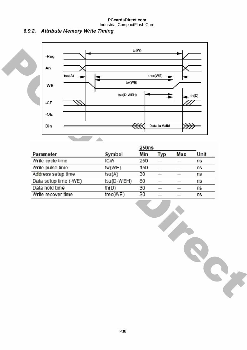
PCcardsDirect
6.9.2. Attribute Memory Write Timing
PCcardsDirect.com Industrial CompactFlash Card
P.18

PC6.9.3. Common Memory Read Timing 6.
PCcardsDirect.com Industrial CompactFlash Card
card9.4. Common Memory Writing Timing
sDirectP.19

PC6.9.5. I/O Input (Read) Timing 6.9
PCcardsDirect.com Industrial CompactFlash Card
cardsDir.6. I/O Output (Writing) Timing
ectP..20
PCcardsDirect
6.9.7. True IDE Mode Read/Write I/O Timing
PCcardsDirect.com Industrial CompactFlash Card
P..21
PCcardsDirect
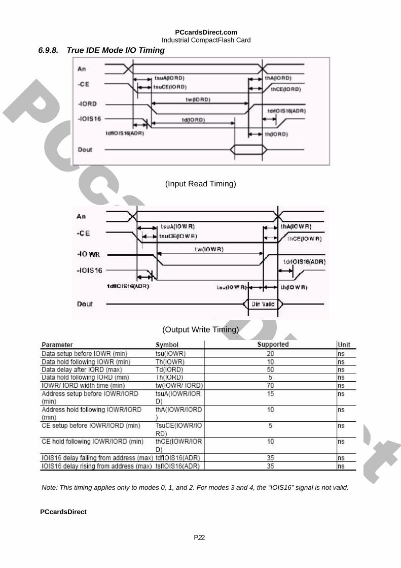
6.9.8. True IDE Mode I/O Timing
(Input Read Timing)
(Output Write Timing)
Note: This timing applies only to modes 0, 1, and 2. For modes 3 and 4, the “IOIS16” signal is not valid.
PCcardsDirect
PCcardsDirect.com Industrial CompactFlash Card
P.22

PCcardsDirect
6.10. CompactFlash Card Registers and Memory Space Decoding
6.10.1. Attribute Memory Function Attribute memory is a space where CompactFlash Storage Card and CF+ Card identification and configuration information are stored, and is limited to 8 bit wide accesses only at even addresses. The card configuration registers are also located here. For CompactFlash Storage Cards, the base address of the card configuration registers is 200h. For CF+ cards, the base address of the card configuration registers is determined by the Configuration tuple (CISTPL_CONFIG). For the Attribute Memory Read function, signals -REG and -OE must be active and -WE inactive during the cycle. As in the Main Memory Read functions, the signals -CE1 and -CE2 control the even-byte and odd-byte address, but only the even-byte data is valid during the Attribute Memory access. Refer to Table 24: Attribute Memory Function below for signal states and bus validity for the Attribute Memory function.
PCcardsDirect.com Industrial CompactFlash Card
P..23

PCcardsDirect
6.10.2. I/O function The I/O transfer to or from the CompactFlash Storage or CF+ Card can be either 8 or 16 bits. When a 16 bit accessible port is addressed, the signal -IOIS16 is asserted by the CompactFlash Storage or CF+ Card. Otherwise, the -IOIS16 signal is de-asserted. When a 16 bit transfer is attempted, and the -IOIS16 signal is not asserted by the CompactFlash Storage or CF+ Card, the system must generate a pair of 8 bit references to access the word‘s even byte and odd byte. The CompactFlash Storage Card permits both 8 and 16 bit accesses to all of its I/O addresses, so -IOIS16 is asserted for all addresses to which the CompactFlash Storage responds. CF+ cards may or may not allow 16 bit register accesses and thus must assert IOIS16 as required. The CompactFlash Storage and CF+ Card may request the host to extend the length of an input cycle until data is ready by asserting the -WAIT signal at the start of the cycle.
PCcardsDirect.com Industrial CompactFlash Card
P..24

PCcardsDirect
6.10.3. Common Memory Function The Common Memory transfer to or from the CompactFlash Storage or CF+ Card can be either 8 or 16 bits .The CompactFlash Storage Card and the CF+ Card permit both 8 and 16 bit accesses to all of its Common Memory addresses. The CompactFlash Storage Card or the CF+ Card may request the host to extend the length of a memory write cycle or extend the length of a memory read cycle until data is ready by asserting the -WAIT signal at the start of the cycle.
PCcardsDirect.com Industrial CompactFlash Card
P..25

PCcardsDirect
6.10.4. True IDE Mode I/O Function The CompactFlash Storage Card and CF+ Card can be configured in a True IDE Mode of operation. The CompactFlash Storage Card is configured in this mode only when the -OE input signal is grounded by the host during the power off to power on cycle. Optionally, CompactFlash Storage Cards and CF+ Cards may support the following optional detection methods: 1. The card is permitted to monitor the –OE (-ATA SEL) signal at any time(s) and switch to PCMCIA mode upon detecting a high level on the pin. 2. The card is permitted to re-arbitrate the interface mode determination following a transition of the (-)RESET pin. 3. The card is permitted to monitor the –OE (-ATA SEL) signal at any time(s) and switch to True IDE mode upon detection of a continuous low level on pin for an extended period of time. Host implementers should not rely on any of these optional detection methods in their designs. In the True IDE Mode, the PCMCIA protocol and configuration are disabled and only I/O operations to the Task File and Data Register are allowed. In this mode, no Memory or Attribute Registers are accessible to the host. CompactFlash Storage Cards permit 8 bit data accesses if the user issues a Set Feature Command to put the CompactFlash Storage Card in 8 bit Mode.
PCcardsDirect.com Industrial CompactFlash Card
P..26

PCcardsDirect
6.11. I/O Primary and Secondary Address Configurations 6.11.1. Primary and Secondary I/O Decoding
6.11.2. Contiguous I/O Mapped Addressing & Decoding When the system decodes a contiguous block of I/O registers to select the CompactFlash Storage Card, the registers are accessed in the block of I/O space decoded by the system as follows:
PCcardsDirect.com Industrial CompactFlash Card
P.27

PCcardsDirect
6.11.3. Memory Mapped Addressing & Decoding When the CompactFlash Storage Card registers are accessed via memory references, the registers appear in the common memory space window: 0-2K bytes as follows:
6.11.4. True IDE Mode Addressing When the CompactFlash Storage Card is configured in the True IDE Mode, the I/O decoding is as follows:
PCcardsDirect.com Industrial CompactFlash Card
P.28

PCcardsDirect
PCcardsDirectPCFLASH’s Industrial CompactFlash Card provides automatic power saving mode. There are four modes on this system: 1. Standby Mode: When the PCcardsDirectPCFLASH’s Industrial CompactFlash finished initialization after power reset or hardware reset, it goes into Standby Mode to wait for Command In or Soft Reset. 2. Active Mode: If the PCcardsDirectPCFLASH’s Industrial CompactFlash received any Command In or Soft Reset, it goes into Active Mode. In Active Mode, it is capable of executing any ATA commands. The power consumption is the greatest in this mode. 3. Sleep Mode: The PCcardsDirectPCFLASH’s Industrial CompactFlash will enter Sleep Mode if there is no Command In or Soft Reset from the host for about 4ms or sleep command is asserted. This time interval can be modified by firmware if necessary. Sleep Mode provides the lowest power consumption. During Sleep Mode, the system main clock is stopped. This mode can be waked up from hardware reset, software reset or any ATA command asserted.
PCcardsDirect.com Industrial CompactFlash Card
P..29

PCcardsDirect
7. CF – ATA Command Description This section defines the software requirements and the format of the commands the host sends to the CompactFlash Storage Cards. Commands are issued to the CompactFlash Storage Card by loading the required registers in the command block with the supplied parameters, and then writing the command code to the Command Register. The manner in which a command is accepted varies. There are three classes (see Table 37: CF-ATA Command Set) of command acceptance, all dependent on the host not issuing commands unless the CompactFlash Storage Card is not busy (BSY=0). All commands listed in this specification shall be implemented. Commands can be implemented as “no operation” to meet this requirement. The Security Mode feature set (command codes F1, F2, F3, F4, F5, and F6) should not be implemented unless the device is intended to be used in an embedded, non-removable application. The Security Mode feature set was not designed for removable devices and certain problems may be encountered when using these commands in a removable application. This specification introduces some new commands and features. If these commands are used on an older CF card, an Invalid Command Error may occur. Upon receipt of a Class 1 command, the CompactFlash Storage Card sets BSY within 400 nsec. Upon receipt of a Class 2 command, the CompactFlash Storage Card sets BSY within 400 nsec, sets up the sector buffer for a write operation, sets DRQ within 700 µsec, and clears BSY within 400 nsec of setting DRQ. Upon receipt of a Class 3 command, the CompactFlash Storage Card sets BSY within 400 nsec, sets up the sector buffer for a write operation, sets DRQ within 20 msec (assuming no re-assignments), and clears BSY within 400 nsec of setting DRQ.
PCcardsDirect.com Industrial CompactFlash Card
P.30

PCcardsDirect
7.1. CF – ATA Command Set CF-ATA Command Set summarizes the CF-ATA command set with the paragraphs that follow describing the individual commands and the task file for each.
PCcardsDirect.com Industrial CompactFlash Card
P.31

PCcardsDirect
Definitions: FR = Features Register SC = Sector Count Register SN = Sector Number Register CY = Cylinder Registers DH = Card/Drive/Head Register LBA = Logical Block Address Mode Supported (see command descriptions for use). Y - The register contains a valid parameter for this command. For the Drive/Head Register Y means both the CompactFlash Storage Card and head parameters are used; D - only the CompactFlash Storage Card parameter is valid and not the head parameter; C – The register contains command specific data (see command descriptions for use).
PCcardsDirect
PCcardsDirect.com Industrial CompactFlash Card
P.32

PCcardsDirect
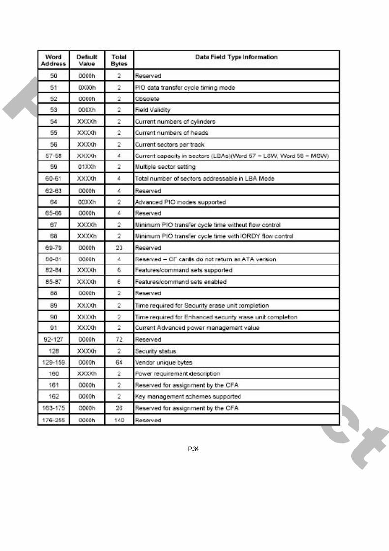
7.1.1. Identify Drive – Ech
The Identify Drive command enables the host to receive parameter information from the CompactFlash Storage Card. This command has the same protocol as the Read Sector(s) command. The parameter words in the buffer have the arrangement and meanings defined in Table 39. All reserved bits or words are zero. Hosts should not depend on Obsolete words in Identify Drive containing 0. Table 39 specifies each field in the data returned by the Identify Drive Command. In Table 39, X indicates a numeric nibble value specific to the card and aaaa indicates an ASCII string specific to the particular drive. 7.1.2. Identify Drive Information
PCcardsDirect.com Industrial CompactFlash Card
P.33
PCcardsDirectH
PCcardsDirect.com Industrial CompactFlash Card
P.34

PCcardsDirect
Word 0: General Configuration This field indicates that the device is a CompactFlash Storage Card. Note to host implementers: If Word 0 of the Identify drive information is 848Ah then the device complies with the CFA specification, not with the ATA-4 specification. Word 1: Default Number of Cylinders This field contains the number of translated cylinders in the default translation mode. This value will be the same as the number of cylinders. Word 3: Default Number of Heads This field contains the number of translated heads in the default translation mode. Word 6: Default Number of Sectors per Track This field contains the number of sectors per track in the default translation mode. Words 7-8: Number of Sectors per Card This field contains the number of sectors per CompactFlash Storage Card. This double word value is also the first invalid address in LBA translation mode. Words 10-19: Serial Number This field contains the serial number for this CompactFlash Storage Card and is right justified and padded with spaces (20h). Word 22: ECC Count This field defines the number of ECC bytes used on each sector in the Read and Write Long commands. This value shall be set to 0004h. Words 23-26: Firmware Revision This field contains the revision of the firmware for this product. Words 27-46: Model Number This field contains the model number for this product and is left justified and padded with spaces (20h). Word 47: Read/Write Multiple Sector Count Bits 15-8 shall be the recommended value of 80h or the permitted value of 00h. Bits 7-0 of this word define the maximum number of sectors per block that the CompactFlash Storage Card supports for Read/Write Multiple commands. Word 49: Capabilities Bit 13: Standby Timer If bit 13 is set to 1 then the Standby timer is supported as defined by the IDLE command If bit 13 is set to 0 then the Standby timer operation is defined by the vendor. Bit 11: IORDY Supported If bit 11 is set to 1 then this CompactFlash Storage Card supports IORDY operation. If bit 11 is set to 0 then this CompactFlash Storage Card may support IORDY operation. Bit 10: IORDY may be disabled Bit 10 shall be set to 0, indicating that IORDY may not be disabled. Bit 9: LBA supported Bit 9 shall be set to 1, indicating that this CompactFlash Storage Card supports LBA mode addressing. CF devices shall support LBA addressing. Bit 8: DMA Supported If bit 8 is set to 1 then Read DMA and Write DMA commands are supported. Bit 8 shall be set to 0. Read/Write DMA commands are not currently permitted on CF cards.
PCcardsDirect.com Industrial CompactFlash Card
P.35

PCcardsDirectH
PCcardsDirect.com Industrial CompactFlash Card
P.34

PCcardsDirect
CompactFlash Storage Card supports a field in words 64-70 other than this field and the CompactFlash Storage Card does not support this field, the CompactFlash Storage Card shall return a value of zero in this field. Word 68: Minimum PIO transfer cycle time with IORDY Word 68 of the parameter information of the Identify Device command is defined as the minimum PIO transfer with IORDY flow control cycle time. This field defines, in nanoseconds, the minimum cycle time that the CompactFlash Storage Card supports while performing data transfers while utilizing IORDY flow control. If this field is supported, Bit 1 of word 53 shall be set to one. Any CompactFlash Storage Card that supports PIO mode 3 or above shall support this field, and the value in word 68 shall be the fastest defined PIO mode supported by the CompactFlash Storage Card. If bit 1 of word 53 is set to one because a CompactFlash Storage Card supports a field in words 64-70 other than this field and the CompactFlash Storage Card does not support this field, the CompactFlash Storage Card shall return a value of zero in this field. Words 82-84: Features/command sets supported Words 82, 83, and 84 shall indicate features/command sets supported. The value 0000h or FFFFh was placed in each of these words by CompactFlash Storage Cards prior to ATA-3 and shall be interpreted by the host as meaning that features/command sets supported are not indicated. Bits 1 through 13 of word 83 and bits 0 through 13 of word 84 are reserved. Bit 14 of word 83 and word 84 shall be set to one and bit 15 of word 83 and word 84 shall be cleared to zero to provide indication that the features/command sets supported words are valid. The values in these words should not be depended on by host implementers. Bit 0 of word 82 shall be set to zero; the SMART feature set is not supported. If bit 1 of word 82 is set to one, the Security Mode feature set is supported. Bit 2 of word 82 shall be set to zero; the Removable Media feature set is not supported. Bit 3 of word 82 shall be set to one; the Power Management feature set is supported. Bit 4 of word 82 shall be set to zero; the Packet Command feature set is not supported. If bit 5 of word 82 is set to one, write cache is supported. If bit 6 of word 82 is set to one, look-ahead is supported. Bit 7 of word 82 shall be set to zero; release interrupt is not supported. Bit 8 of word 82 shall be set to zero; Service interrupt is not supported. Bit 9 of word 82 shall be set to zero; the Device Reset command is not supported. Bit 10 of word 82 shall be set to zero; the Host Protected Area feature set is not supported. Bit 11 of word 82 is obsolete. Bit 12 of word 82 shall be set to one; the CompactFlash Storage Card supports the Write Buffer command. Bit 13 of word 82 shall be set to one; the CompactFlash Storage Card supports the Read Buffer command. Bit 14 of word 82 shall be set to one; the CompactFlash Storage Card supports the NOP
PCcardsDirect.com Industrial CompactFlash Card
P.37

PCcardsDirect
command. Bit 15 of word 82 is obsolete. Bit 0 of word 83 shall be set to zero; the CompactFlash Storage Card does not support the Download Microcode command. Bit 1 of word 83 shall be set to zero; the CompactFlash Storage Card does not support the Read DMA Queued and Write DMA Queued commands. Bit 2 of word 83 shall be set to one; the CompactFlash Storage Card supports the CFA feature set. If bit 3 of word 83 is set to one, the CompactFlash Storage Card supports the Advanced Power Management feature set. Bit 4 of word 83 shall be set to zero; the CompactFlash Storage Card does not support the Removable Media Status feature set. Words 85-87: Features/command sets enabled Words 85, 86, and 87 shall indicate features/command sets enabled. The value 0000h or FFFFh was placed in each of these words by CompactFlash Storage Cards prior to ATA-4 and shall be interpreted by the host as meaning that features/command sets enabled are not indicated. Bits 1 through 15 of word 86 are reserved. Bits 0-13 of word 87 are reserved. Bit 14 of word 87 shall be set to one and bit 15 of word 87 shall be cleared to zero to provide indication that the features/command sets enabled words are valid. The values in these words should not be depended on by host implementers. Bit 0 of word 85 shall be set to zero; the SMART feature set is not enabled. If bit 1 of word 85 is set to one, the Security Mode feature set has been enabled via the Security Set Password command. Bit 2 of word 85 shall be set to zero; the Removable Media feature set is not supported. Bit 3 of word 85 shall be set to one; the Power Management feature set is supported. Bit 4 of word 85 shall be set to zero; the Packet Command feature set is not enabled. If bit 5 of word 85 is set to one, write cache is enabled. If bit 6 of word 85 is set to one, look-ahead is enabled. Bit 7 of word 85 shall be set to zero; release interrupt is not enabled. Bit 8 of word 85 shall be set to zero; Service interrupt is not enabled. Bit 9 of word 85 shall be set to zero; the Device Reset command is not supported. Bit 10 of word 85 shall be set to zero; the Host Protected Area feature set is not supported. Bit 11 of word 85 is obsolete. Bit 12 of word 85 shall be set to one; the CompactFlash Storage Card supports the Write Buffer command. Bit 13 of word 85 shall be set to one; the CompactFlash Storage Card supports the Read Buffer command. Bit 14 of word 85 shall be set to one; the CompactFlash Storage Card supports the NOP
PCcardsDirect.com Industrial CompactFlash Card
P.38

PCcardsDirect
command. Bit 15 of word 85 is obsolete. Bit 0 of word 86 shall be set to zero; the CompactFlash Storage Card does not support the Download Microcode command. Bit 1 of word 86 shall be set to zero; the CompactFlash Storage Card does not support the Read DMA Queued and Write DMA Queued commands. If bit 2 of word 86 shall be set to one, the CompactFlash Storage Card supports the CFA feature set. If bit 3 of word 86 is set to one, the Advanced Power Management feature set has been enabled via the Set Features command. Bit 4 of word 86 shall be set to zero; the CompactFlash Storage Card does not support the Removable Media Status feature set. Word 89: Time required for Security erase unit completion Word 89 specifies the time required for the Security Erase Unit command to complete. This command shall be supported on CompactFlash Storage Cards that support security. Value Time 0 Value not specified 1-254 (Value * 2) minute 255 >508 minutes Word 90: Time required for Enhanced security erase unit completion Word 90 specifies the time required for the Enhanced Security Erase Unit command to complete. This command shall be supported on CompactFlash Storage Cards that support security. Value Time 0 Value not specified 1-254 (Value * 2) minutes 255 >508 minutes Word 91: Advanced power management level value Bits 7-0 of word 91 contain the current Advanced Power Management level setting. Word 128: Security Status Bit 8: Security Level If set to 1, indicates that security mode is enabled and the security level is maximum. If set to 0 and security mode is enabled, indicates that the security level is high.
PCcardsDirect.com Industrial CompactFlash Card
P.39

PCcardsDirect
Bit 5: Enhanced security erase unit feature supported If set to 1, indicates that the Enhanced security erase unit feature set is supported. Bit 4: Expire If set to 1, indicates that the security count has expired and Security Unlock and Security Erase Unit are command aborted until a power-on reset or hard reset. Bit 3: Freeze If set to 1, indicates that the security is Frozen. Bit 2: Lock If set to 1, indicates that the security is locked. Bit 1: Enable/Disable If set to 1, indicates that the security is enabled. If set to 0, indicates that the security is disabled. Bit 0: Capability If set to 1, indicates that CompactFlash Storage Card supports security mode feature set. If set to 0, indicates that CompactFlash Storage Card does not support security mode feature set. Word 160: Power Requirement Description This word is required for CompactFlash Storage Cards that support power mode 1. Bit 15: VLD If set to 1, indicates that this word contains a valid power requirement description. If set to 0, indicates that this word does not contain a power requirement description. Bit 14: RSV This bit is reserved and must be 0. Bit 13: -XP If set to 1, indicates that the CompactFlash Storage Card does not have Power Level 1 commands. If set to 0, indicates that the CompactFlash Storage Card has Power Level 1 commands Bit 12: -XE If set to 1, indicates that Power Level 1 commands are disabled. If set to 0, indicates that Power Level 1 commands are enabled. Bit 0-11: Maximum current This field contains the CompactFlash Storage Card’s maximum current in mA. Word 162: Key Management Schemes Supported Bit 0: CPRM support If set to 1, the device supports CPRM Scheme (Content Protection for Recordable Media) If set to 0, the device does not support CPRM. Bits 1-15 are reserved for future additional Key Management schemes.
PCcardsDirect.com Industrial CompactFlash Card
P.40

PCcardsDirect
PCcardsDirect.com Industrial CompactFlash Card
P.41
Clock Input Timing
Parameter Symbol Min Typ. Max Unit
Operating Speed Fop 0 28.4 40 MHz Clock Period Tcp 25 35 - ns Clock High Tch 12.5 17.5 - ns Clock Low Tcl 12.5 17.5 - ns
Notes:
1. The clock may be stopped indefinitely in either state.
2. The Tcp specification is used as a reference in other specifications.
Hard Reset Timing
Above technical information is based on industry standard data and tested to be reliable. However, PCcardsDirectPCFLASH makes no warranty, either expressed or implied, as to its accuracy and assumes no liability in connection with the use of this product. PCcardsDirectPCFLASH reserves the right to make changes in specifications at any time without prior notice.

PCcardsDirect
PCcardsDirect.com Industrial CompactFlash Card
P.42
APPENDIX A. Order Information 1. Part Number
2.5" and 3.5’’ Flash Disk Drive
Capacity 2.5" Industrial Temp. Drive
32MB FDK25I-32MB FDK35I-32MB
64MB FDK25I-64MB FDK35I-64MB
128MB FDK25I-128MB FDK35I-128MB
256MB FDK25I-256MB FDK35I-256MB
512MB FDK25I-512MB FDK35I-512MB
1GB FDK25I-1024MB FDK35I-1024MB
2GB FDK25I-2048MB FDK35I-2048MB
4GB FDK25I-4096MB FDK35I-4096MB
2. Part Number Decoder X1X2X3X4X5-X 6X7X8X9X10X11–X12X1~ X5 = Product Model Name FCFI:CompactFlash ModuleFPCI:PCMCIA ATA Flash Card FDK25I, FDK35I:Flash Disk Drive Module FMDI: Flash Disk Module I = Industrial Temperature, Industrial Grade
3.5" Industrial Temp. Drive

![UD info Corp. Flash Card (CFC)-50SI...-IORD -WE -IOWR RESET -CSEL D[15:0] -PDIAG -DASP INTRQ IORDY -IOCS16 -DMARQ Host CF Card Interface VCC POR VDT Regulator Flash Controller Data](https://img.pdfslide.us/doc/110x75/5af410bd7f8b9a9e598c274a/ud-info-corp-flash-card-cfc-50si-iord-we-iowr-reset-csel-d150-pdiag.jpg)