Embed Size (px)
Citation preview
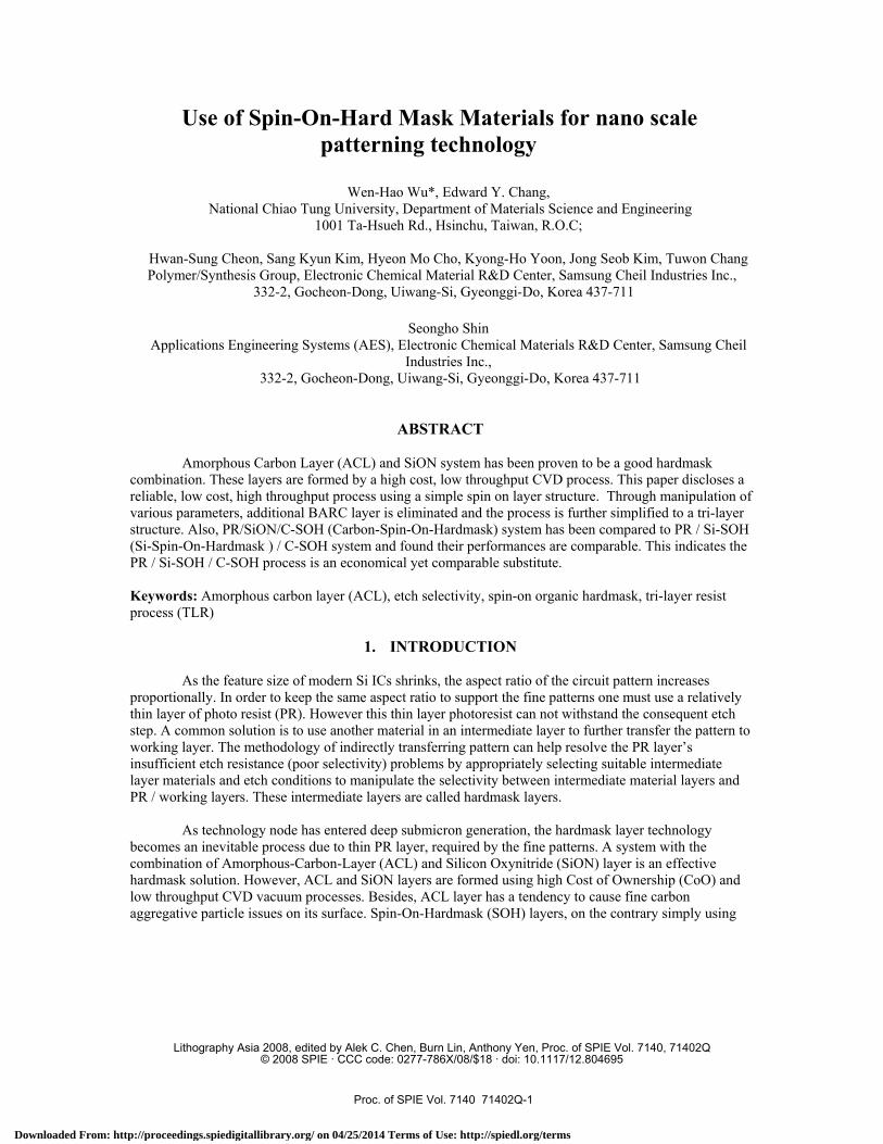
Use of Spin-On-Hard Mask Materials for nano scale patterning technology
Wen-Hao Wu*, Edward Y. Chang,
National Chiao Tung University, Department of Materials Science and Engineering 1001 Ta-Hsueh Rd., Hsinchu, Taiwan, R.O.C;
Hwan-Sung Cheon, Sang Kyun Kim, Hyeon Mo Cho, Kyong-Ho Yoon, Jong Seob Kim, Tuwon Chang Polymer/Synthesis Group, Electronic Chemical Material R&D Center, Samsung Cheil Industries Inc.,
332-2, Gocheon-Dong, Uiwang-Si, Gyeonggi-Do, Korea 437-711
Seongho Shin Applications Engineering Systems (AES), Electronic Chemical Materials R&D Center, Samsung Cheil
Industries Inc., 332-2, Gocheon-Dong, Uiwang-Si, Gyeonggi-Do, Korea 437-711
ABSTRACT
Amorphous Carbon Layer (ACL) and SiON system has been proven to be a good hardmask combination. These layers are formed by a high cost, low throughput CVD process. This paper discloses a reliable, low cost, high throughput process using a simple spin on layer structure. Through manipulation of various parameters, additional BARC layer is eliminated and the process is further simplified to a tri-layer structure. Also, PR/SiON/C-SOH (Carbon-Spin-On-Hardmask) system has been compared to PR / Si-SOH (Si-Spin-On-Hardmask ) / C-SOH system and found their performances are comparable. This indicates the PR / Si-SOH / C-SOH process is an economical yet comparable substitute. Keywords: Amorphous carbon layer (ACL), etch selectivity, spin-on organic hardmask, tri-layer resist process (TLR)
1. INTRODUCTION
As the feature size of modern Si ICs shrinks, the aspect ratio of the circuit pattern increases
proportionally. In order to keep the same aspect ratio to support the fine patterns one must use a relatively thin layer of photo resist (PR). However this thin layer photoresist can not withstand the consequent etch step. A common solution is to use another material in an intermediate layer to further transfer the pattern to working layer. The methodology of indirectly transferring pattern can help resolve the PR layer’s insufficient etch resistance (poor selectivity) problems by appropriately selecting suitable intermediate layer materials and etch conditions to manipulate the selectivity between intermediate material layers and PR / working layers. These intermediate layers are called hardmask layers.
As technology node has entered deep submicron generation, the hardmask layer technology
becomes an inevitable process due to thin PR layer, required by the fine patterns. A system with the combination of Amorphous-Carbon-Layer (ACL) and Silicon Oxynitride (SiON) layer is an effective hardmask solution. However, ACL and SiON layers are formed using high Cost of Ownership (CoO) and low throughput CVD vacuum processes. Besides, ACL layer has a tendency to cause fine carbon aggregative particle issues on its surface. Spin-On-Hardmask (SOH) layers, on the contrary simply using
Lithography Asia 2008, edited by Alek C. Chen, Burn Lin, Anthony Yen, Proc. of SPIE Vol. 7140, 71402Q© 2008 SPIE · CCC code: 0277-786X/08/$18 · doi: 10.1117/12.804695
Proc. of SPIE Vol. 7140 71402Q-1
Downloaded From: http://proceedings.spiedigitallibrary.org/ on 04/25/2014 Terms of Use: http://spiedl.org/terms
the spin coating technology, can provide an effective alternative to achieve comparably to costly and problematic ACL / SiON process. In this paper we use Silicon-Spin-On-Hardmask (Si-SOH) / Carbon-Spin On Hardmask (C-SOH) combination from Samsung Cheil Industries as a good hardmask solution.
Through the manipulation of Si layer composition, thickness, and its n and k values, these
hardmask layers can show adequate antireflective properties, so we do not need to apply an additional Bottom Anti-Reflective Coating (BARC) layer, and as a result, the process is simplified to a tri-layer spin on structure.
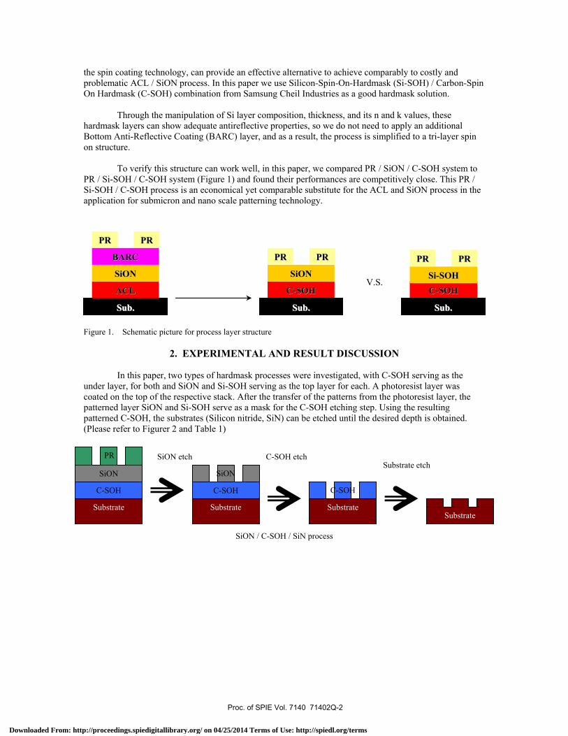
To verify this structure can work well, in this paper, we compared PR / SiON / C-SOH system to
PR / Si-SOH / C-SOH system (Figure 1) and found their performances are competitively close. This PR / Si-SOH / C-SOH process is an economical yet comparable substitute for the ACL and SiON process in the application for submicron and nano scale patterning technology.
C-HM Figure 1. Schematic picture for process layer structure
2. EXPERIMENTAL AND RESULT DISCUSSION
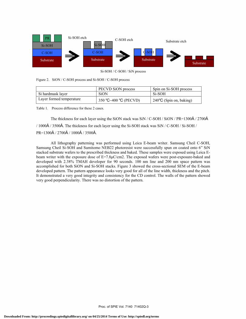
In this paper, two types of hardmask processes were investigated, with C-SOH serving as the
under layer, for both and SiON and Si-SOH serving as the top layer for each. A photoresist layer was coated on the top of the respective stack. After the transfer of the patterns from the photoresist layer, the patterned layer SiON and Si-SOH serve as a mask for the C-SOH etching step. Using the resulting patterned C-SOH, the substrates (Silicon nitride, SiN) can be etched until the desired depth is obtained. (Please refer to Figurer 2 and Table 1)
SiON / C-SOH / SiN process
CC--SSOOHHV.S.
CC--SSOOHH
SSiiOONN
SSuubb..
AACCLL
SSiiOONN
PPRR PPRR
BBAARRCC
SSuubb.. SSuubb..
SSii--SSOOHH
C-SOH
SiON
C-SOH
Substrate Substrate Substrate
Substrate
SiON etch C-SOH etch Substrate etch
SiON
C-SOH
PR
PPRR PPRR PPRR PPRR
Proc. of SPIE Vol. 7140 71402Q-2
Downloaded From: http://proceedings.spiedigitallibrary.org/ on 04/25/2014 Terms of Use: http://spiedl.org/terms
Si-SOH / C-SOH / SiN process
Figure 2. SiON / C-SOH process and Si-SOH / C-SOH process
Table 1. Process difference for these 2 cases. The thickness for each layer using the SiON stack was SiN / C-SOH / SiON / PR=1300Å / 2700Å
/ 1000Å / 3500Å. The thickness for each layer using the Si-SOH stack was SiN / C-SOH / Si-SOH /
PR=1300Å / 2700Å / 1000Å / 3500Å. All lithography patterning was performed using Leica E-beam writer. Samsung Cheil C-SOH,
Samsung Cheil Si-SOH and Sumitomo NEB22 photoresist were successfully spun on coated onto 6” SiN stacked substrate wafers to the prescribed thickness and baked. These samples were exposed using Leica E-beam writer with the exposure dose of E=7.8µC/cm2. The exposed wafers were post-exposure-baked and developed with 2.38% TMAH developer for 90 seconds. 100 nm line and 200 nm space pattern was accomplished for both SiON and Si-SOH stacks. Figure 3 showed the cross-sectional SEM of the E-beam developed pattern. The pattern appearance looks very good for all of the line width, thickness and the pitch. It demonstrated a very good integrity and consistency for the CD control. The walls of the pattern showed very good perpendicularity. There was no distortion of the pattern.
PECVD SiON process Spin on Si-SOH process Si hardmask layer SiON Si-SOH Layer formed temperature 350 ℃~400 ℃ (PECVD) 240℃ (Spin on, baking)
Substrate Substrate
C-SOH
Si-SOH
Substrate
C-SOH
Substrate
Si-SOH etch Substrate etch C-SOH etch
Si-SOH
C-SOH
PR
Proc. of SPIE Vol. 7140 71402Q-3
Downloaded From: http://proceedings.spiedigitallibrary.org/ on 04/25/2014 Terms of Use: http://spiedl.org/terms
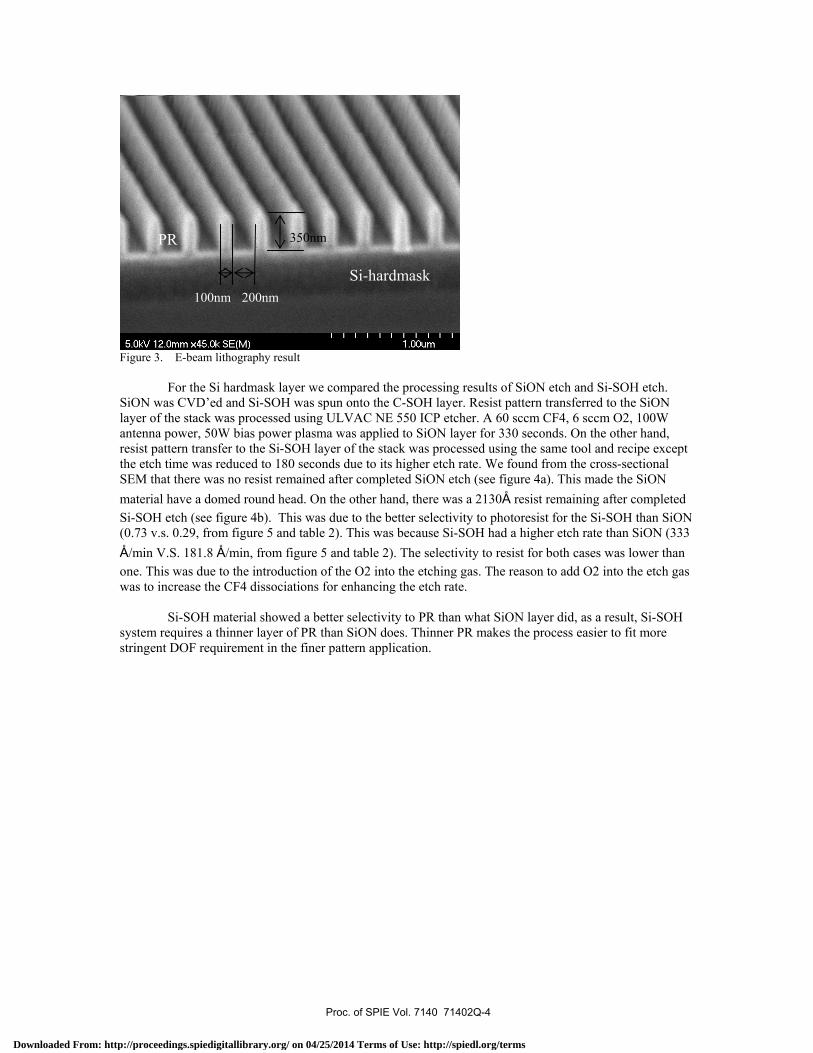
Figure 3. E-beam lithography result
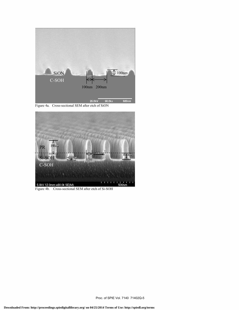
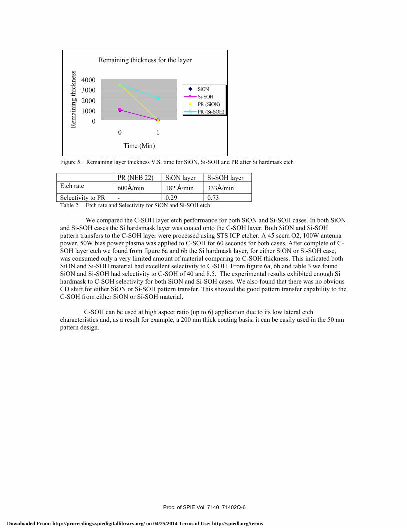
For the Si hardmask layer we compared the processing results of SiON etch and Si-SOH etch.
SiON was CVD’ed and Si-SOH was spun onto the C-SOH layer. Resist pattern transferred to the SiON layer of the stack was processed using ULVAC NE 550 ICP etcher. A 60 sccm CF4, 6 sccm O2, 100W antenna power, 50W bias power plasma was applied to SiON layer for 330 seconds. On the other hand, resist pattern transfer to the Si-SOH layer of the stack was processed using the same tool and recipe except the etch time was reduced to 180 seconds due to its higher etch rate. We found from the cross-sectional SEM that there was no resist remained after completed SiON etch (see figure 4a). This made the SiON material have a domed round head. On the other hand, there was a 2130Å resist remaining after completed Si-SOH etch (see figure 4b). This was due to the better selectivity to photoresist for the Si-SOH than SiON (0.73 v.s. 0.29, from figure 5 and table 2). This was because Si-SOH had a higher etch rate than SiON (333 Å/min V.S. 181.8 Å/min, from figure 5 and table 2). The selectivity to resist for both cases was lower than one. This was due to the introduction of the O2 into the etching gas. The reason to add O2 into the etch gas was to increase the CF4 dissociations for enhancing the etch rate.
Si-SOH material showed a better selectivity to PR than what SiON layer did, as a result, Si-SOH
system requires a thinner layer of PR than SiON does. Thinner PR makes the process easier to fit more stringent DOF requirement in the finer pattern application.
PR 350nm
200nm 100nm Si-hardmask
Proc. of SPIE Vol. 7140 71402Q-4
Downloaded From: http://proceedings.spiedigitallibrary.org/ on 04/25/2014 Terms of Use: http://spiedl.org/terms
25.0kv 90.Okx 500nm
Figure 4a. Cross-sectional SEM after etch of SiON
Figure 4b. Cross-sectional SEM after etch of Si-SOH
SiON
Si-SOH
PR
100nm
100nm 200nm
102nm C-SOH
C-SOH
Proc. of SPIE Vol. 7140 71402Q-5
Downloaded From: http://proceedings.spiedigitallibrary.org/ on 04/25/2014 Terms of Use: http://spiedl.org/terms
Remaining thickness for the layer
01000200030004000
0 1
Time (Min)
Rem
aini
ng th
ickn
ess
SiONSi-SOHPR (SiON)PR (Si-SOH)
Figure 5. Remaining layer thickness V.S. time for SiON, Si-SOH and PR after Si hardmask etch PR (NEB 22) SiON layer Si-SOH layer Etch rate 600Å/min 182 Å/min 333Å/min Selectivity to PR - 0.29 0.73 Table 2. Etch rate and Selectivity for SiON and Si-SOH etch
We compared the C-SOH layer etch performance for both SiON and Si-SOH cases. In both SiON
and Si-SOH cases the Si hardsmask layer was coated onto the C-SOH layer. Both SiON and Si-SOH pattern transfers to the C-SOH layer were processed using STS ICP etcher. A 45 sccm O2, 100W antenna power, 50W bias power plasma was applied to C-SOH for 60 seconds for both cases. After complete of C-SOH layer etch we found from figure 6a and 6b the Si hardmask layer, for either SiON or Si-SOH case, was consumed only a very limited amount of material comparing to C-SOH thickness. This indicated both SiON and Si-SOH material had excellent selectivity to C-SOH. From figure 6a, 6b and table 3 we found SiON and Si-SOH had selectivity to C-SOH of 40 and 8.5. The experimental results exhibited enough Si hardmask to C-SOH selectivity for both SiON and Si-SOH cases. We also found that there was no obvious CD shift for either SiON or Si-SOH pattern transfer. This showed the good pattern transfer capability to the C-SOH from either SiON or Si-SOH material.
C-SOH can be used at high aspect ratio (up to 6) application due to its low lateral etch
characteristics and, as a result for example, a 200 nm thick coating basis, it can be easily used in the 50 nm pattern design.
Proc. of SPIE Vol. 7140 71402Q-6
Downloaded From: http://proceedings.spiedigitallibrary.org/ on 04/25/2014 Terms of Use: http://spiedl.org/terms
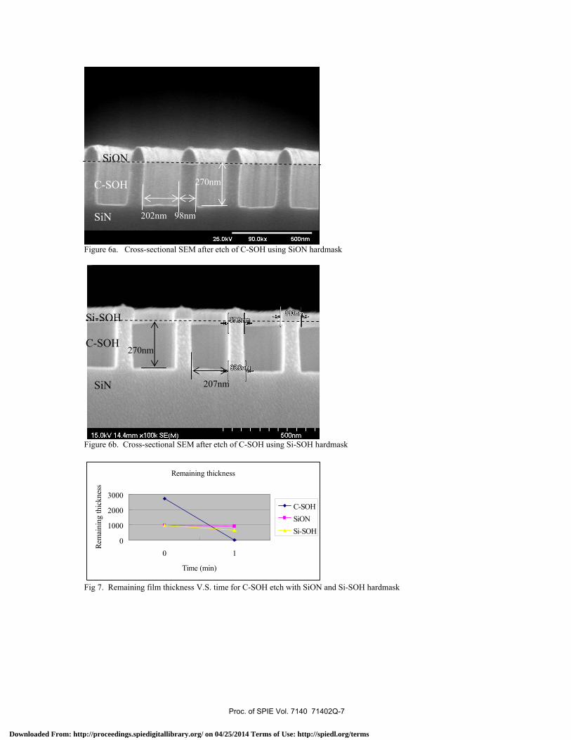
Figure 6a. Cross-sectional SEM after etch of C-SOH using SiON hardmask
Figure 6b. Cross-sectional SEM after etch of C-SOH using Si-SOH hardmask
Remaining thickness
0
1000
2000
3000
0 1
Time (min)
Rem
aini
ng th
ickn
ess
C-SOHSiONSi-SOH
Fig 7. Remaining film thickness V.S. time for C-SOH etch with SiON and Si-SOH hardmask
C-SOH
SiON
Si-SOH
C-SOH
202nm
207nm
270nm
98nm
270nm
SiN
SiN
Proc. of SPIE Vol. 7140 71402Q-7
Downloaded From: http://proceedings.spiedigitallibrary.org/ on 04/25/2014 Terms of Use: http://spiedl.org/terms
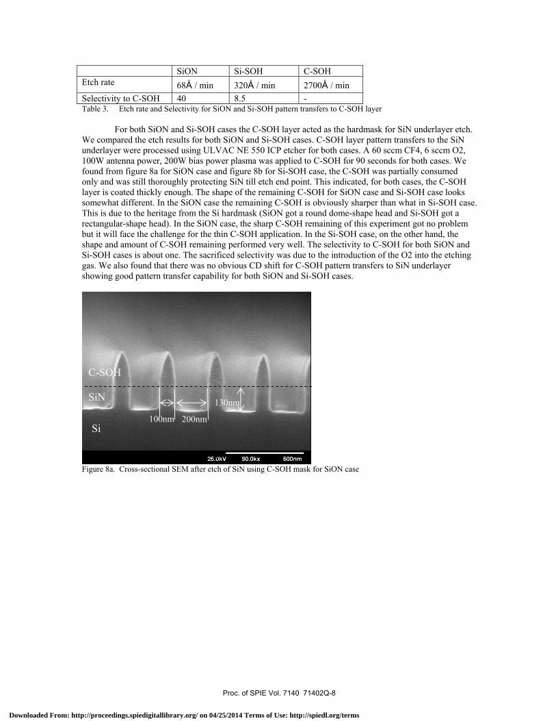
SiON Si-SOH C-SOH Etch rate 68Å / min 320Å / min 2700Å / min Selectivity to C-SOH 40 8.5 - Table 3. Etch rate and Selectivity for SiON and Si-SOH pattern transfers to C-SOH layer
For both SiON and Si-SOH cases the C-SOH layer acted as the hardmask for SiN underlayer etch.
We compared the etch results for both SiON and Si-SOH cases. C-SOH layer pattern transfers to the SiN underlayer were processed using ULVAC NE 550 ICP etcher for both cases. A 60 sccm CF4, 6 sccm O2, 100W antenna power, 200W bias power plasma was applied to C-SOH for 90 seconds for both cases. We found from figure 8a for SiON case and figure 8b for Si-SOH case, the C-SOH was partially consumed only and was still thoroughly protecting SiN till etch end point. This indicated, for both cases, the C-SOH layer is coated thickly enough. The shape of the remaining C-SOH for SiON case and Si-SOH case looks somewhat different. In the SiON case the remaining C-SOH is obviously sharper than what in Si-SOH case. This is due to the heritage from the Si hardmask (SiON got a round dome-shape head and Si-SOH got a rectangular-shape head). In the SiON case, the sharp C-SOH remaining of this experiment got no problem but it will face the challenge for the thin C-SOH application. In the Si-SOH case, on the other hand, the shape and amount of C-SOH remaining performed very well. The selectivity to C-SOH for both SiON and Si-SOH cases is about one. The sacrificed selectivity was due to the introduction of the O2 into the etching gas. We also found that there was no obvious CD shift for C-SOH pattern transfers to SiN underlayer showing good pattern transfer capability for both SiON and Si-SOH cases.
Figure 8a. Cross-sectional SEM after etch of SiN using C-SOH mask for SiON case
C-SOH
SiN
Si
130nm
100nm 200nm
Proc. of SPIE Vol. 7140 71402Q-8
Downloaded From: http://proceedings.spiedigitallibrary.org/ on 04/25/2014 Terms of Use: http://spiedl.org/terms
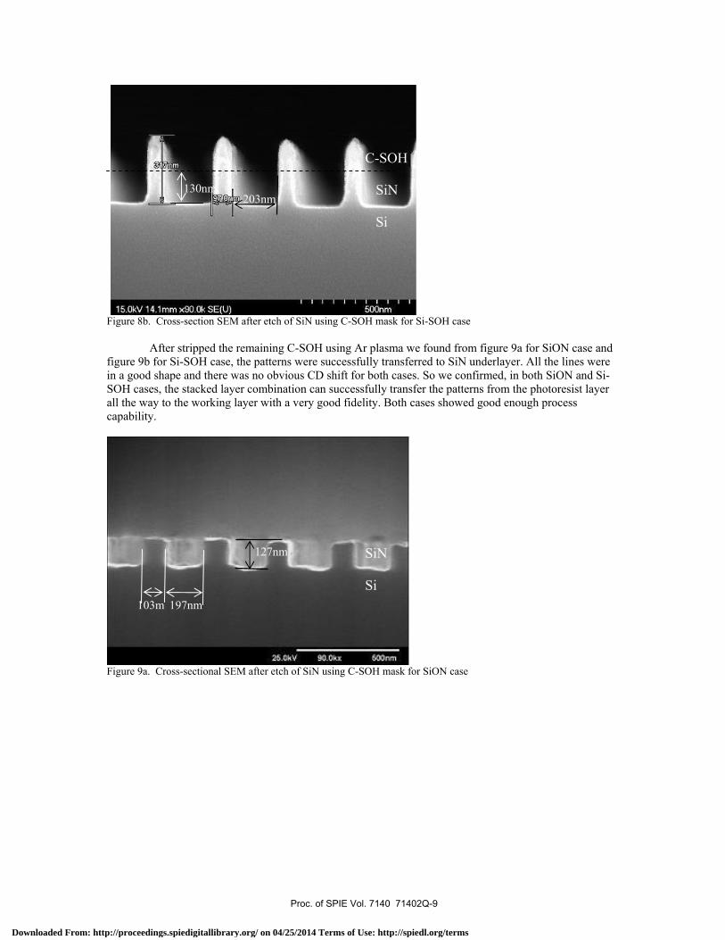
Figure 8b. Cross-section SEM after etch of SiN using C-SOH mask for Si-SOH case
After stripped the remaining C-SOH using Ar plasma we found from figure 9a for SiON case and figure 9b for Si-SOH case, the patterns were successfully transferred to SiN underlayer. All the lines were in a good shape and there was no obvious CD shift for both cases. So we confirmed, in both SiON and Si-SOH cases, the stacked layer combination can successfully transfer the patterns from the photoresist layer all the way to the working layer with a very good fidelity. Both cases showed good enough process capability.
Figure 9a. Cross-sectional SEM after etch of SiN using C-SOH mask for SiON case
C-SOH
Si
203nm 130nm
197nm 103m
127nm SiN
Si
SiN
Proc. of SPIE Vol. 7140 71402Q-9
Downloaded From: http://proceedings.spiedigitallibrary.org/ on 04/25/2014 Terms of Use: http://spiedl.org/terms
900kz 600nm
rsaLiii90.Okx SOOnm
Figure 9b. Cross-section SEM after etch of SiN using C-SOH mask for Si-SOH case
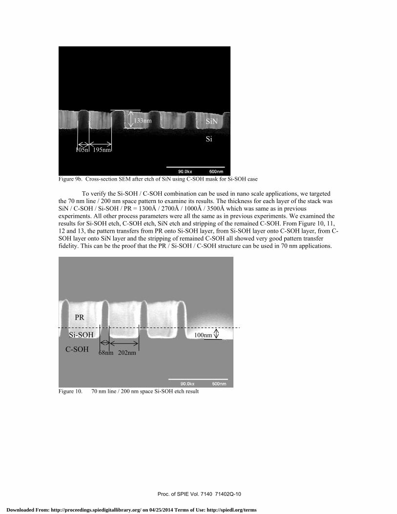
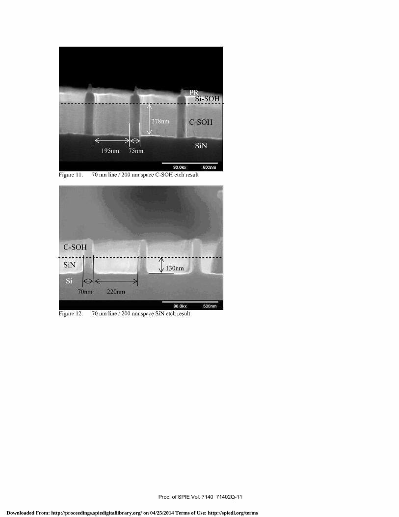
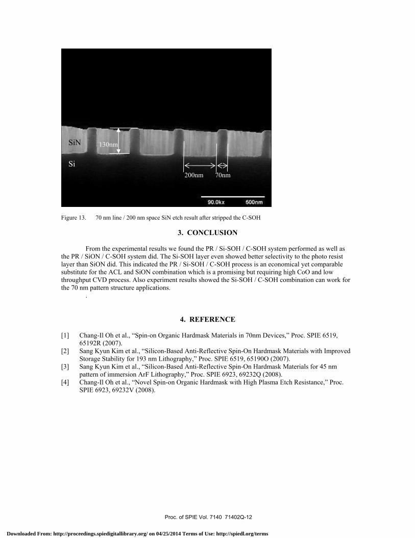
To verify the Si-SOH / C-SOH combination can be used in nano scale applications, we targeted the 70 nm line / 200 nm space pattern to examine its results. The thickness for each layer of the stack was SiN / C-SOH / Si-SOH / PR = 1300Å / 2700Å / 1000Å / 3500Å which was same as in previous experiments. All other process parameters were all the same as in previous experiments. We examined the results for Si-SOH etch, C-SOH etch, SiN etch and stripping of the remained C-SOH. From Figure 10, 11, 12 and 13, the pattern transfers from PR onto Si-SOH layer, from Si-SOH layer onto C-SOH layer, from C-SOH layer onto SiN layer and the stripping of remained C-SOH all showed very good pattern transfer fidelity. This can be the proof that the PR / Si-SOH / C-SOH structure can be used in 70 nm applications.
Figure 10. 70 nm line / 200 nm space Si-SOH etch result
PR
Si-SOH
68nm
100nm
202nm
105n 195nm
133nm
C-SOH
SiN
Si
Proc. of SPIE Vol. 7140 71402Q-10
Downloaded From: http://proceedings.spiedigitallibrary.org/ on 04/25/2014 Terms of Use: http://spiedl.org/terms
90.Okx bOOnn,
Figure 11. 70 nm line / 200 nm space C-SOH etch result
Figure 12. 70 nm line / 200 nm space SiN etch result
SiN
C-SOH
SiN
C-SOH 278nm
75nm 195nm
130nm
220nm 70nm
Si-SOH
Si
PR
Proc. of SPIE Vol. 7140 71402Q-11
Downloaded From: http://proceedings.spiedigitallibrary.org/ on 04/25/2014 Terms of Use: http://spiedl.org/terms
9Ox 500mm
Figure 13. 70 nm line / 200 nm space SiN etch result after stripped the C-SOH
3. CONCLUSION
From the experimental results we found the PR / Si-SOH / C-SOH system performed as well as the PR / SiON / C-SOH system did. The Si-SOH layer even showed better selectivity to the photo resist layer than SiON did. This indicated the PR / Si-SOH / C-SOH process is an economical yet comparable substitute for the ACL and SiON combination which is a promising but requiring high CoO and low throughput CVD process. Also experiment results showed the Si-SOH / C-SOH combination can work for the 70 nm pattern structure applications.
.
4. REFERENCE
[1] Chang-Il Oh et al., “Spin-on Organic Hardmask Materials in 70nm Devices,” Proc. SPIE 6519, 65192R (2007).
[2] Sang Kyun Kim et al., “Silicon-Based Anti-Reflective Spin-On Hardmask Materials with Improved Storage Stability for 193 nm Lithography,” Proc. SPIE 6519, 65190O (2007).
[3] Sang Kyun Kim et al., “Silicon-Based Anti-Reflective Spin-On Hardmask Materials for 45 nm pattern of immersion ArF Lithography,” Proc. SPIE 6923, 69232Q (2008).
[4] Chang-Il Oh et al., “Novel Spin-on Organic Hardmask with High Plasma Etch Resistance,” Proc. SPIE 6923, 69232V (2008).
70nm200nm
SiN
Si
130nm
Proc. of SPIE Vol. 7140 71402Q-12
Downloaded From: http://proceedings.spiedigitallibrary.org/ on 04/25/2014 Terms of Use: http://spiedl.org/terms


![1 2 arXiv:2008.08357v1 [cond-mat.mes-hall] 19 Aug 2020arXiv:2008.08357v1 [cond-mat.mes-hall] 19 Aug 2020 Impact of intra-grain spin wave reflections on nano-contact spin torque oscillators](https://img.pdfslide.us/doc/110x75/60a8d4fa3c4ded631a64978b/1-2-arxiv200808357v1-cond-matmes-hall-19-aug-2020-arxiv200808357v1-cond-matmes-hall.jpg)