Embed Size (px)
Citation preview

PocketProfessional™ Series
EE•Pro ®
#UQHVYCTG#RRNKECVKQP1P6+CPF6+2NWU
User’s Guide
June 1999© da Vinci Technologies Group, Inc.
Rev. 1.0
da Vinci Technologies Group, Inc.1600 S.W. Western Blvd
Suite 250Corvallis, OR 97333
www.dvtg.com

Notice
This manual and the examples contained herein are provided “as is” as a supplement to EE•Proapplication software available from Texas Instruments for TI-89, and 92 Plus platforms. Da VinciTechnologies Group, Inc. (“da Vinci”) makes no warranty of any kind with regard to thismanual or the accompanying software, including, but not limited to, the implied warranties ofmerchantability and fitness for a particular purpose. Da Vinci shall not be liable for any errors orfor incidental or consequential damages in connection with the furnishing, performance, or use of thismanual, or the examples herein.
Copyright da Vinci Technologies Group, Inc. 1999. All rights reserved.PocketProfessional and EE•Pro is a registered trademarks of da Vinci Technologies Group, Inc.
We welcome your comments on the software and the manual. Forward your comments, preferably bye-mail to da Vinci at [email protected].
AcknowledgementsThe EE•Pro software was developed by Dave Conklin, Casey Walsh, Michael Conway and Megha Shyam with thegenerous support of TI’s development team. The user’s guide was developed by Michael Conway and MeghaShyam. Many helpful comments from the testers at Texas Instruments and other locations during β testing phase isgratefully acknowledged.
Table of Contents1 Introduction to EE•Pro.. . . . . . . . . . . . . . . . . . . . . . . . . . . . . . . . . . . . . . . . . . . . . . . . . . . . . . . i
1.1 Key Features of EE•Pro . . . . . . . . . . . . . . . . . . . . . . . . . . . . . . . . . . . . . . . . . . . . . . . . i 1.2 Download/Purchase Information . . . . . . . . . . . . . . . . . . . . . . . . . . . . . . . . . . . . . . . . . ii 1.3 Manual Ordering . . . . . . . . . . . . . . . . . . . . . . . . . . . . . . . . . . . . . . . . . . . . . . . . . . . . . . ii 1.4 Memory Requirements . . . . . . . . . . . . . . . . . . . . . . . . . . . . . . . . . . . . . . . . . . . . . . . . . ii 1.5 Differences between TI-89 and TI-92 plus . . . . . . . . . . . . . . . . . . . . . . . . . . . . . . . . . . iii 1.6 Beginning EE•Pro. . . . . . . . . . . . . . . . . . . . . . . . . . . . . . . . . . . . . . . . . . . . . . . . . . . . . iii 1.7 Manual Organization. . . . . . . . . . . . . . . . . . . . . . . . . . . . . . . . . . . . . . . . . . . . . . . . . . . iii 1.8 Disclaimer. . . . . . . . . . . . . . . . . . . . . . . . . . . . . . . . . . . . . . . . . . . . . . . . . . . . . . . . . . . iv 1.9 Summary. . . . . . . . . . . . . . . . . . . . . . . . . . . . . . . . . . . . . . . . . . . . . . . . . . . . . . . . . . . . iv
Part I: Analysis
2 Introduction to Analysis . . . . . . . . . . . . . . . . . . . . . . . . . . . . . . . . . . . . . . . . . . . . . . . . . . . . . 1
2.1 Introduction . . . . . . . . . . . . . . . . . . . . . . . . . . . . . . . . . . . . . . . . . . . . . . . . . . . . . . . . . 1 2.2 Setting up an Analysis Problem . . . . . . . . . . . . . . . . . . . . . . . . . . . . . . . . . . . . . . . . . . 1 2.3 Solving Problems in Analysis . . . . . . . . . . . . . . . . . . . . . . . . . . . . . . . . . . . . . . . . . . . 32.4 Special Function Keys in Analysis Routines . . . . . . . . . . . . . . . . . . . . . . . . . . . . . . . . .4 2.5 Data Fields, Analysis Functions and Sample Problems . . . . . . . . . . . . . . . . . . . . . . . . 5
Example 2.1 . . . . . . . . . . . . . . . . . . . . . . . . . . . . . . . . . . . . . . . . . . . . . . . . . . . . . . 7Example 2.2 . . . . . . . . . . . . . . . . . . . . . . . . . . . . . . . . . . . . . . . . . . . . . . . . . . . . . . 7Example 2.3 . . . . . . . . . . . . . . . . . . . . . . . . . . . . . . . . . . . . . . . . . . . . . . . . . . . . . . 8
2.6 Session Folders, Variable Names . . . . . . . . . . . . . . . . . . . . . . . . . . . . . . . . . . . . . . . . . 9
3 AC Circuits . . . . . . . . . . . . . . . . . . . . . . . . . . . . . . . . . . . . . . . . . . . . . . . . . . . . . . . . . . . . . . . . 103.1 Impedance Calculations . . . . . . . . . . . . . . . . . . . . . . . . . . . . . . . . . . . . . . . . . . . . . . . . 10
Example 3.1 . . . . . . . . . . . . . . . . . . . . . . . . . . . . . . . . . . . . . . . . . . . . . . . . . . . . . 113.2 Voltage Divider . . . . . . . . . . . . . . . . . . . . . . . . . . . . . . . . . . . . . . . . . . . . . . . . . . . . . . 11
Example 3.2 . . . . . . . . . . . . . . . . . . . . . . . . . . . . . . . . . . . . . . . . . . . . . . . . . . . . . . 113.3 Current Divider . . . . . . . . . . . . . . . . . . . . . . . . . . . . . . . . . . . . . . . . . . . . . . . . . . . . . . . 12
Example 3.3 . . . . . . . . . . . . . . . . . . . . . . . . . . . . . . . . . . . . . . . . . . . . . . . . . . . . . . 123.4 Circuit Performance . . . . . . . . . . . . . . . . . . . . . . . . . . . . . . . . . . . . . . . . . . . . . . . . . . . 13
Example 3.4 . . . . . . . . . . . . . . . . . . . . . . . . . . . . . . . . . . . . . . . . . . . . . . . . . . . . . . 14
4 Polyphase Circuits . . . . . . . . . . . . . . . . . . . . . . . . . . . . . . . . . . . . . . . . . . . . . . . . . . . . . . . . . . . 154.1 Wye ↔∆ Conversion . . . . . . . . . . . . . . . . . . . . . . . . . . . . . . . . . . . . . . . . . . . . . . . . . . 15
Example 4.1. . . . . . . . . . . . . . . . . . . . . . . . . . . . . . . . . . . . . . . . . . . . . . . . . . . . . . 164.2 Balanced Wye Load . . . . . . . . . . . . . . . . . . . . . . . . . . . . . . . . . . . . . . . . . . . . . . . . . . . 16
Example 4.2 . . . . . . . . . . . . . . . . . . . . . . . . . . . . . . . . . . . . . . . . . . . . . . . . . . . . . 174.3 Balanced ∆ Load . . . . . . . . . . . . . . . . . . . . . . . . . . . . . . . . . . . . . . . . . . . . . . . . . . . . . 17
Example 4.3 . . . . . . . . . . . . . . . . . . . .. . . . . . . . . . . . . . . . . . . . . . . . . . . . . . . . . . 18
5 Ladder network . . . . . . . . . . . . . . . . . . . . . . . . . . . . . . . . . . . . . . . . . . . . . . . . . . . . . . . . . . . . . 195.1 Using Ladder Network . . . . . . . . . . . . . . . . . . . . . . . . . . . . . . . . . . . . . . . . . . . . . . . . 195.2 Using the Ladder Network . . . . . . . . . . . . . . . . . . . . . . . . . . . . . . . . . . . . . . . . . . . . . . 22
Example 5.1 . . . . . . . . . . . . . . . . . . . . . . . . . . . . . . . . . . . . . . . . . . . . . . . . . . . . . 22Example 5.2 . . . . . . . . . . . . . . . . . . . . . . . . . . . . . . . . . . . . . . . . . . . . . . . . . . . . . 23
6 Filter Design . . . . . . . . . . . . . . . . . . . . . . . . . . . . . . . . . . . . . . . . . . . . . . . . . . . . . . . . . . . . . . . 256.1 Chebyshev Filter . . . . . . . . . . . . . . . . . . . . . . . . . . . . . . . . . . . . . . . . . . . . . . . . . . . . . .25
Example 6.1. . . . . . . . . . . . . . . . . . . . . . . . . . . . . . . . . . . . . . . . . . . . . . . . . . . . . . 266.2 Butterworth Filter . . . . . . . . . . . . . . . . . . . . . . . . . . . . . . . . . . . . . . . . . . . . . . . . . . . . .26
Example 6.2 . . . . . . . . . . . . . . . . . . . . . . . . . . . . . . . . . . . . . . . . . . . . . . . . . . . . . . 27 6.3 Active Filters . . . . . . . . . . . . . . . . . . . . . . . . . . . . . . . . . . . . . . . . . . . . . . . . . . . . . . . . 27
Example 6.3 . . . . . . . . . . . . . . . . . . . . . . . . . . . . . . . . . . . . . . . . . . . . . . . . . . . . . . 28
7 Gain and Frequency . . . . . . . . . . . . . . . . . . . . . . . . . . . . . . . . . . . . . . . . . . . . . . . . . . . . . . . . . 297.1 Transfer Function . . . . . . . . . . . . . . . . . . . . . . . . . . . . . . . . . . . . . . . . . . . . . . . . . . . . . 29
Example 7.1 . . . . . . . . . . . . . . . . . . . . . . . . . . . . . . . . . . . . . . . . . . . . . . . . . . . . . . 307.2 Bode Diagrams . . . . . . . . . . . . . . . . . . . . . . . . . . . . . . . . . . . . . . . . . . . . . . . . . . . . . . . 30
Example 7.2 . . . . . . . . . . . . . . . . . . . . . . . . . . . . . . . . . . . . . . . . . . . . . . . . . . . . . . 31
8 Fourier Transforms . . . . . . . . . . . . . . . . . . . . . . . . . . . . . . . . . . . . . . . . . . . . . . . . . . . . . . . . . 328.1 FFT . . . . . . . . . . . . . . . . . . . . . . . . . . . . . . . . . . . . . . . . . . . . . . . . . . . . . . . . . . . . . . . . 32
Example 8.1 . . . . . . . . . . . . . . . . . . . . . . . . . . . . . . . . . . . . . . . . . . . . . . . . . . . . . . 328.2 Inverse FFT . . . . . . . . . . . . . . . . . . . . . . . . . . . . . . . . . . . . . . . . . . . . . . . . . . . . . . . . . . 33
Example 8.2 . . . . . . . . . . . . . . . . . . . . . . . . . . . . . . . . . . . . . . . . . . . . . . . . . . . . . 33
9 Two-Port Networks . . . . . . . . . . . . . . . . . . . . . . . . . . . . . . . . . . . . . . . . . . . . . . . . . . . . . . . . . . 349.1 Parameter Conversion . . . . . . . . . . . . . . . . . . . . . . . . . . . . . . . . . . . . . . . . . . . . . . . . . . 34
Example 9.1 . . . . . . . . . . . . . . . . . . . . . . . . . . . . . . . . . . . . . . . . . . . . . . . . . . . . . . 359.2 Circuit Performance. . . . . . . . . . . . . . . . . . . . . . . . . . . . . . . . . . . . . . . . . . . . . . . . . . . . 36
Example 9.2 . . . . . . . . . . . . . . . . . . . . . . . . . . . . . . . . . . . . . . . . . . . . . . . . . . . . . . 379.3 Connected Two-Ports . . . . . . . . . . . . . . . . . . . . . . . . . . . . . . . . . . . . . . . . . . . . . . . . . . 37
Example 9.3 . . . . . . . . . . . . . . . . . . . . . . . . . . . . . . . . . . . . . . . . . . . . . . . . . . . . . . 38
10 Transformer Calculations. . . . . . . . . . . . . . . . . . . . . . . . . . . . . . . . . . . . . . . . . . . . . . . . . . . . . 3910.1 Open Circuit Test . . . . . . . . . . . . . . . . . . . . . . . . . . . . . . . . . . . . . . . . . . . . . . . . . . . 39
Example 10.1 . . . . . . . . . . . . . . . . . . . . . . . . . . . . . . . . . . . . . . . . . . . . . . . . . . . . . 3910.2 Short Circuit Test . . . . . . . . . . . . . . . . . . . . . . . . . . . . . . . . . . . . . . . . . . . . . . . . . . . .40
Example 10.2 . . . . . . . . . . . . . . . . . . . . . . . . . . . . . . . . . . . . . . . . . . . . . . . . . . . . . 4010.3 Chain Parameters . . . . . . . . . . . . . . . . . . . . . . . . . . . . . . . . . . . . . . . . . . . . . . . . . . . .41
Example 10.3 . . . . . . . . . . . . . . . . . . . . . . . . . . . . . . . . . . . . . . . . . . . . . . . . . . . . . 42
11 Transmission Lines . . . . . . . . . . . . . . . . . . . . . . . . . . . . . . . . . . . . . . . . . . . . . . . . . . . . . . . . . . 4311.1 Line Properties . . . . . . . . . . . . . . . . . . . . . . . . . . . . . . . . . . . . . . . . . . . . . . . . . . . . . 43
Example 11.1 . . . . . . . . . . . . . . . . . . . . . . . . . . . . . . . . . . . . . . . . . . . . . . . . . . . . 4411.2 Line Parameters . . . . . . . . . . . . . . . . . . . . . . . . . . . . . . . . . . . . . . . . . . . . . . . . . . . . . 44
Example 11.2 . . . . . . . . . . . . . . . . . . . . . . . . . . . . . . . . . . . . . . . . . . . . . . . . . . . . . 4511.3 Fault Location Estimate . . . . . . . . . . . . . . . . . . . . . . . . . . . . . . . . . . . . . . . . . . . . . . 45
Example 11.3 . . . . . . . . . . . . .. . . . . . . . . . . . . . . . . . . . . . . . . . . . . . . . . . . . . . . . 4611.4 Stub Impedance Matching . . . . . . . . . . . . . . . . . . . . . . . . . . . . . . . . . . . . . . . . . . . .46
Example 11.4 . . . . . . . . . . . . . . . . . . . . . . . . . . . . . . . . . . . . . . . . . . . . . . . . . . . . . 47
12 Computer Engineering. . . . . . . . . . . . . . . . . . . . . . . . . . . . . . . . . . . . . . . . . . . . . . . . . . . . . . . 4812.1 Special Mode Settings, the † Key . . . . . . . . . . . . . . . . . . . . . . . . . . . . . . . . . . . . . .4812.2 Binary Arithmetic . . . . . . . . . . . . . . . . . . . . . . . . . . . . . . . . . . . . . . . . . . . . . . . . . . . .50
Example 12.2 . . . . . . . . . . . . . . . . . . . . . . . . . . . . . . . . . . . . . . . . . . . . . . . . . . . . . 5012.3 Register Operations . . . . . . . . . . . . . . . . . . . . . . . . . . . . . . . . . . . . . . . . . . . . . . . . . . 51
Example 12.3 . . . . . . . . . . . . . . . . . . . . . . . . . . . . . . . . . . . . . . . . . . . . . . . . . . . . . 5212.4 Bit Operations . . . . . . . . . . . . . . . . . . . . . . . . . . . . . . . . . . . . . . . . . . . . . . . . . . . . . . 52
Example 12.4 . . . . . . . . . . . . . . . . . . . . . . . . . . . . . . . . . . . . . . . . . . . . . . . . . . . . . 53
12.5 Binary Conversions . . . . . . . . . . . . . . . . . . . . . . . . . . . . . . . . . . . . . . . . . . . . . . . . . . 53Example 12.5 . . . . . . . . . . . . . . . . . . . . . . . . . . . . . . . . . . . . . . . . . . . . . . . . . . . . . 54
12.6 Binary Comparisons . . . . . . . . . . . . . . . . . . . . . . . . . . . . . . . . . . . . . . . . . . . . . . . . . 54Example 12.6 . . . . . . . . . . . . . . . . . . . . . . . . . . . . . . . . . . . . . . . . . . . . . . . . . . . . 55
12.7 Karnaugh Map . . . . . . . . . . . . . . . . . . . . . . . . . . . . . . . . . . . . . . . . . . . . . . . . . . . . . .55Example 12.7 . . . . . . . . . . . . . . . . . . . . . . . . . . . . . . . . . . . . . . . . . . . . . . . . . . . . 56
13 Error Functions. . . . . . . . . . . . . . . . . . . . . . . . . . . . . . . . . . . . . . . . . . . . . . . . . . . . . . . . . . . . . 5713.1 Using Error Function . . . . . . . . . . . . . . . . . . . . . . . . . . . . . . . . . . . . . . . . . . . . . . . . 57
Example 13.1 . . . . . . . . . . . . . . . . . . . . . . . . . . . . . . . . . . . . . . . . . . . . . . . . . . . . 57
14 Capital Budgeting . . . . . . . . . . . . . . . . . . . . . . . . . . . . . . . . . . . . . . . . . . . . . . . . . . . . . . . . . . . 5814.1 Using Capital Budgeting . . . . . . . . . . . . . . . . . . . . . . . . . . . . . . . . . . . . . . . . . . . . . . 58
Example 14.1 . . . . . . . . . . . . . . . . . . . . . . . . . . . . . . . . . . . . . . . . . . . . . . . . . . . . . 59
Part II: Equations
15 Introduction to Equations . . . . . . . . . . . . . . . . . . . . . . . . . . . . . . . . . . . . . . . . . . . . . . . . . . . . 115.1 Solving a set of Equations. . . . . . . . . . . . . . . . . . . . . . . . . . . . . . . . . . . . . . . . . . . . . 115.2 Viewing an Equation or Result in Pretty Print . . . . . . . . . . . . . . . . . . . . . . . . . . . . . 215.3 Viewing a Result in different units. . .. . . . . . . . . . . . . . . . . . . . . . . . . . . . . . . . . . . . 215.4 Viewing Multiple Solutions. . . . . . . . . . . . . . . . . . . . . . . . . . . . . . . . . . . . . . . . . . . . 315.5 Partial Solutions. . . . . . . . . . . . . . . . . . . . . . . . . . . . . . . . . . . . . . . . . . . . . . . . . . . . . 315.6 Copy/Paste. . . . . . . . . . . . . . . . . . . . . . . . . . . . . . . . . . . . . . . . . . . . . . . . . . . . . . . . . 415.7 Graphing a Function. . . . . . . . . . . . . . . . . . . . . . . . . . . . . . . . . . . . . . . . . . . . . . . . . .415.8 Storing and recalling variable values in EE•Pro-creation of session folders . . . . . . 515.9 solve, nsolve, and csolve and user-defined functions (UDF) . . . . . . . . . . . . . . . . . . 615.10 Entering a guess value for the unknown using nsolve. . . . . . . . . . . . . . . . . . . . . . . . 615.11 Why can't I compute a solution?. . . . . . . . . . . . . . . . . . . . . . . . . . . . . . . . . . . . . . . . 615.12 Care in choosing a consistent set of equations . . . . . . . . . . . . . . . . . . . . . . . . . . . . . 715.13 Notes for the advanced user in troubleshooting calculations. . . . . . . . . . . . . . . . . . . 7
16 Resistive Circuits . . . . . . . . . . . . . . . . . . . . . . . . . . . . . . . . . . . . . . . . . . . . . . . . . . . . . . . . . . . 9Variables . . . . . . . . . . . . . . . . . . . . . . . . . . . . . . . . . . . . . . . . . . . . . . . . . . . . . . . . . . . . . . . . . 9
16.1 Resistance Formulas . . . . . . . . . . . . . . . . . . . . . . . . . . . . . . . . . . . . . . . . . . . . . . . . . 9Example 16.1 . . . . . . . . . . . . . . . . . . . . . . . . . . . . . . . . . . . . . . . . . . . . . . . . . . . . . 10
16.2 Ohm’s Law and Power . . . . . . . . . . . . . . . . . . . . . . . . . . . . . . . . . . . . . . . . . . . . . . . 10Example 16.2 . . . . . . . . . . . . . . . . . . . . . . . . . . . . . . . . . . . . . . . . . . . . . . . . . . . . 10
16.3 Temperature Effect on resistance . . .. . . . . . . . . . . . . . . . . . . . . . . . . . . . . . . . . . . . 11Example 16.3 . . . . . . . . . . . . . . . . . . . . . . . . . . . . . . . . . . . . . . . . . . . . . . . . . . . . . 11
16.4 Maximum Power Transfer . . . . . . . . . . . . . . . . . . . . . . . . . . . . . . . . . . . . . . . . . . . . 12Example 16.4 . . . . . . . . . . . . . . . . . . . . . . . . . . . . . . . . . . . . . . . . . . . . . . . . . . . . 12
16.5 Voltage and Current Source Equivalence . . . . . . . . . . . . . . . . . . . . . . . . . . . . . . . . 13Example 16.5 . . . . . . . . . . . . . . . . . . . . . . . . . . . . . . . . . . . . . . . . . . . . . . . . . . . . 13
17 Capacitors and Electric Fields . . . . . . . . . . . . . . . . . . . . . . . . . . . . . . . . . . . . . . . . . . . . . . . . 14Variables . . . . . . . . . . . . . . . . . . . . . . . . . . . . . . . . . . . . . . . . . . . . . . . . . . . . . . . . . . . . . . . . . 14
17.1 Point Charge . . . . . . . . . . . . . . . . . . . . . . . . . . . . . . . . . . . . . . . . . . . . . . . . . . . . . . .15Example 17.1 . . . . . . . . . . . . . . . . . . . . . . . . . . . . . . . . . . . . . . . . . . . . . . . . . . . . 15
17.2 Long Charged Line . . . . . . . . . . . . . . . . . . . . . . . . . . . . . . . . . . . . . . . . . . . . . . . . . .15Example 17.2 . . . . . . . . . . . . . . . . . . . . . . . . . . . . . . . . . . . . . . . . . . . . . . . . . . . . . 15
17.3 Charged Disk . . . . . . . . . . . . . . . . . . . . . . . . . . . . . . . . . . . . . . . . . . . . . . . . . . . . . . . 16Example 17.3 . . . . . . . . . . . . . . . . . . . . . . . . . . . . . . . . . . . . . . . . . . . . . . . . . . . . . 16
17.4 Parallel Plates . . . . . . . . . . . . . . . . . . . . . . . . . . . . . . . . . . . . . . . . . . . . . . . . . . . . . . 17 Example 17.4 . . . . . . . . . . . . . . . . . . . . . . . . . . . . . . . . . . . . . . . . . . . . . . . . . . . . . 17
17.5 Parallel Wires . . . . . . . . . . . . . . . . . . . . . . . . . . . . . . . . . . . . . . . . . . . . . . . . . . . . . . 17Example 17.5 . . . . . . . . . . . . . . . . . . . . . . . . . . . . . . . . . . . . . . . . . . . . . . . . . . . . 18
17.6 Coaxial Cable . . . . . . . . . . . . . . . . . . . . . . . . . . . . . . . . . . . . . . . . . . . . . . . . . . . . . . 18Example 17.6 . . . . . . . . . . . . . . . . . . . . . . . . . . . . . . . . . . . . . . . . . . . . . . . . . . . . 18
17.7 Sphere . . . . . . . . . . . . . . . . . . . . . . . . . . . . . . . . . . . . . . . . . . . . . . . . . . . . . . . . . . . . 19Example 17.7 . . . . . . . . . . . . . . . . . . . . . . . . . . . . . . . . . . . . . . . . . . . . . . . . . . . . . 19
18 Inductors and Magnetism . . . . . . . . . . . . . . . . . . . . . . . . . . . . . . . . . . . . . . . . . . . . . . . . . . . . . 21Variables . . . . . . . . . . . . . . . . . . . . . . . . . . . . . . . . . . . . . . . . . . . . . . . . . . . . . . . . . . . . . . . . . 21
18.1 Long Line . . . . . . . . . . . . . . . . . . . . . . . . . . . . . . . . . . . . . . . . . . . . . . . . . . . . . . . . . 22Example 18.1 . . . . . . . . . . . . . . . . . . . . . . . . . . . . . . . . . . . . . . . . . . . . . . . . . . . . . 22
18.2 Long Strip . . . . . . . . . . . . . . . . . . . . . . . . . . . . . . . . . . . . . . . . . . . . . . . . . . . . . . . . . 22Example 18.2 . . . . . . . . . . . . . . . . . . . . . . . . . . . . . . . . . . . . . . . . . . . . . . . . . . . . . 23
18.3 Parallel Wires . . . . . . . . . . . . . . . . . . . . . . . . . . . . . . . . . . . . . . . . . . . . . . . . . . . . . . 23Example 18.3 . . . . . . . . . . . . . . . . . . . . . . . . . . . . . . . . . . . . . . . . . . . . . . . . . . . . . 23
18.4 Loop . . . . . . . . . . . . . . . . . . . . . . . . . . . . . . . . . . . . . . . . . . . . . . . . . . . . . . . . . . . . . 24Example 18.4 . . . . . . . . . . . . . . . . . . . . . . . . . . . . . . . . . . . . . . . . . . . . . . . . . . . . . 24
18.5 Coaxial Cable . . . . . . . . . . . . . . . . . . . . . . . . . . . . . . . . . . . . . . . . . . . . . . . . . . . . . . 25Example 18.5 . . . . . . . . . . . . . . . . . . . . . . . . . . . . . . . . . . . . . . . . . . . . . . . . . . . . . 25
18.6 Skin Effect . . . . . . . . . . . . . . . . . . . . . . . . . . . . . . . . . . . . . . . . . . . . . . . . . . . . . . . . . 25Example 18.6 . . . . . . . . . . . . . . . . . . . . . . . . . . . . . . . . . . . . . . . . . . . . . . . . . . . . . 26
19 Electron Motion . . . . . . . . . . . . . . . . . . . . . . . . . . . . . . . . . . . . . . . . . . . . . . . . . . . . . . . . . . . . 27Variables . . . . . . . . . . . . . . . . . . . . . . . . . . . . . . . . . . . . . . . . . . . . . . . . . . . . . . . . . . . . . . . . . 27
19.1 Beam Deflection . . . . . . . . . . . . . . . . . . . . . . . . . . . . . . . . . . . . . . . . . . . . . . . . . . . . 27Example 19.1 . . . . . . . . . . . . . . . . . . . . . . . . . . . . . . . . . . . . . . . . . . . . . . . . . . . . . 28
19.2 Thermionic Emission . . . . . . . . . . . . . . . . . . . . . . . . . . . . . . . . . . . . . . . . . . . . . . . . 29Example 19.2 . . . . . . . . . . . . . . . . . . . . . . . . . . . . . . . . . . . . . . . . . . . . . . . . . . . . 29
19.3 Photoemission . . . . . . . . . . . . . . . . . . . . . . . . . . . . . . . . . . . . . . . . . . . . . . . . . . . . . .29Example 19.3 . . . . . . . . . . . . . . . . . . . . . . . . . . . . . . . . . . . . . . . . . . . . . . . . . . . . . 29
20 Meters and Bridge Circuits . . . . . . . . . . . . . . . . . . . . . . . . . . . . . . . . . . . . . . . . . . . . . . . . . . . 31Variables . . . . . . . . . . . . . . . . . . . . . . . . . . . . . . . . . . . . . . . . . . . . . . . . . . . . . . . . . . . . . . . . 31
20.1 A, V, Ω Meters . . . . . . . . . . . . . . . . . . . . . . . . . . . . . . . . . . . . . . . . . . . . . . . . . . . . . 32Example 20.1 . . . . . . . . . . . . . . . . . . . . . . . . . . . . . . . . . . . . . . . . . . . . . . . . . . . . . 32
20.2 Wheatstone Bridge . . . . . . . . . . . . . . . . . . . . . . . . . . . . . . . . . . . . . . . . . . . . . . . . . . 33Example 20.2 . . . . . . . . . . . . . . . . . . . . . . . . . . . . . . . . . . . . . . . . . . . . . . . . . . . . . 33
20.3 Wien Bridge . . . . . . . . . . . . . . . . . . . . . . . . . . . . . . . . . . . . . . . . . . . . . . . . . . . . . . . 34Example 20.3 . . . . . . . . . . . . . . . . . . . . . . . . . . . . . . . . . . . . . . . . . . . . . . . . . . . . . 34
20.4 Maxwell Bridge . . . . . . . . . . . . . . . . . . . . . . . . . . . . . . . . . . . . . . . . . . . . . . . . . . . . . 35Example 20.4 . . . . . . . . . . . . . . . . . . . . . . . . . . . . . . . . . . . . . . . . . . . . . . . . . . . . 35
20.5 Owen Bridge . . . . . . . . . . . . . . . . . . . . . . . . . . . . . . . . . . . . . . . . . . . . . . . . . . . . . . 35Example 20.5 . . . . . . . . . . . . . . . . . . . . . . . . . . . . . . . . . . . . . . . . . . . . . . . . . . . . . 36
20.6 Symmetrical Resistive Attenuator . . . . . . . . . . . . . . . . . . . . . . . . . . . . . . . . . . . . . . . 36Example 20.6 . . . . . . . . . . . . . . . . . . . . . . . . . . . . . . . . . . . . . . . . . . . . . . . . . . . . . 37
20.7 Unsymmetrical Resistive Attenuator . . . . . . . . . . . . . . . . . . . . . . . . . . . . . . . . . . . . . 37Example 20.7 . . . . . . . . . . . . . . . . . . . . . . . . . . . . . . . . . . . . . . . . . . . . . . . . . . . . . 38
21 RL and RC Circuits . . . . . . . . . . . . . . . . . . . . . . . . . . . . . . . . . . . . . . . . . . . . . . . . . . . . . . . . . 39Variables . . . . . . . . . . . . . . . . . . . . . . . . . . . . . . . . . . . . . . . . . . . . . . . . . . . . . . . . . . . . . . . . . 39
21.1 RL Natural Response . . . . . . . . . . . . . . . . . . . . . . . . . . . . . . . . . . . . . . . . . . . . . . . . .40Example 21.1 . . . . . . . . . . . . . . . . . . . . . . . . . . . . . . . . . . . . . . . . . . . . . . . . . . . . 40
21.2 RC Natural Response . . . . . . . . . . . . . . . . . . . . . . . . . . . . . . . . . . . . . . . . . . . . . . . 40Example 21.2 . . . . . . . . . . . . . . . . . . . . . . . . . . . . . . . . . . . . . . . . . . . . . . . . . . . . 41
21.3 RL Step Response . . . . . . . . . . . . . . . . . . . . . . . . . . . . . . . . . . . . . . . . . . . . . . . . . . 41Example 21.3 . . . . . . . . . . . . . . . . . . . . . . . . . . . . . . . . . . . . . . . . . . . . . . . . . . . . . 42
21.4 RC Step Response . . . . . . . . . . . . . . . . . . . . . . . . . . . . . . . . . . . . . . . . . . . . . . . . . . . 42Example 21.4 . . . . . . . . . . . . . . . . . . . . . . . . . . . . . . . . . . . . . . . . . . . . . . . . . . . . . 42
21.5 RL Series-Parallel . . . . . . . . . . . . . . . . . . . . . . . . . . . . . . . . . . . . . . . . . . . . . . . . . . . 43Example 21.5 . . . . . . . . . . . . . . . . . . . . . . . . . . . . . . . . . . . . . . . . . . . . . . . . . . . . . 43
21.6 RC Series-Parallel . . . . . . . . . . . . . . . . . . . . . . . . . . . . . . . . . . . . . . . . . . . . . . . . . . . 44Example 21.6 . . . . . . . . . . . . . . . . . . . . . . . . . . . . . . . . . . . . . . . . . . . . . . . . . . . . . 45
22 RLC Circuits . . . . . . . . . . . . . . . . . . . . . . . . . . . . . . . . . . . . . . . . . . . . . . . . . . . . . . . . . . . . . . 46Variables . . . . . . . . . . . . . . . . . . . . . . . . . . . . . . . . . . . . . . . . . . . . . . . . . . . . . . . . . . . . . . . . . 46
22.1 Series Impedance . . . . . . . . . . . . . . . . . . . . . . . . . . . . . . . . . . . . . . . . . . . . . . . . . . . 47Example 22.1 . . . . . . . . . . . . . . . . . . . . . . . . . . . . . . . . . . . . . . . . . . . . . . . . . . . . . 47
22.2 Parallel Admittance . . . . . . . . . . . . . . . . . . . . . . . . . . . . . . . . . . . . . . . . . . . . . . . . . . 48Example 22.2 . . . . . . . . . . . . . . . . . . . . . . . . . . . . . . . . . . . . . . . . . . . . . . . . . . . . . 48
22.3 RLC Natural Response . . . . . . . . . . . . . . . . . . . . . . . . . . . . . . . . . . . . . . . . . . . . . . . 48 Example 22.3 . . . . . . . . . . . . . . . . . . . . . . . . . . . . . . . . . . . . . . . . . . . . . . . . . . . . . 49
22.4 Underdamped Transient Case . . . . . . . . . . . . . . . . . . . . . . . . . . . . . . . . . . . . . . . . . .49Example 22.4 . . . . . . . . . . . . . . . . . . . . . . . . . . . . . . . . . . . . . . . . . . . . . . . . . . . . . 50
22.5 Critically-Damped Transient Case . . . . . . . . . . . . . . . . . . . . . . . . . . . . . . . . . . . . . . 50Example 22.5 . . . . . . . . . . . . . . . . . . . . . . . . . . . . . . . . . . . . . . . . . . . . . . . . . . . . . 51
22.6 Overdamped Transient Case . . . . . . . . . . . . . . . . . . . . . . . . . . . . . . . . . . . . . . . . . . .51Example 22.6 . . . . . . . . . . . . . . . . . . . . . . . . . . . . . . . . . . . . . . . . . . . . . . . . . . . . . 52
23 AC Circuits . . . . . . . . . . . . . . . . . . . . . . . . . . . . . . . . . . . . . . . . . . . . . . . . . . . . . . . . . . . . . . . . 53Variables . . . . . . . . . . . . . . . . . . . . . . . . . . . . . . . . . . . . . . . . . . . . . . . . . . . . . . . . . . . . . . . . . 53
23.1 RL Series Impedance . . . . . . . . . . . . . . . . . . . . . . . . . . . . . . . . . . . . . . . . . . . . . . . . 54Example 23.1 . . . . . . . . . . . . . . . . . . . . . . . . . . . . . . . . . . . . . . . . . . . . . . . . . . . . 54
23.2 RC Series Impedance . . . . . . . . . . . . . . . . . . . . . . . . . . . . . . . . . . . . . . . . . . . . . . . 55Example 23.2 . . . . . . . . . . . . . . . . . . . . . . . . . . . . . . . . . . . . . . . . . . . . . . . . . . . . 55
23.3 Impedance↔Admittance . . . . . . . . . . . . . . . . . . . . . . . . . . . . . . . . . . . . . . . . . . . . 56Example 23.3 . . . . . . . . . . . . . . . . . . . . . . . . . . . . . . . . . . . . . . . . . . . . . . . . . . . . 56
23.4 Two Impedances in Series . . . . . . . . . . . . . . . . . . . . . . . . . . . . . . . . . . . . . . . . . . . . . 56Example 23.4 . . . . . . . . . . . . . . . . . . . . . . . . . . . . . . . . . . . . . . . . . . . . . . . . . . . . 57
23.5 Two Impedances in Parallel . . . . . . . . . . . . . . . . . . . . . . . . . . . . . . . . . . . . . . . . . . . 57Example 23.5 . . . . . . . . . . . . . . . . . . . . . . . . . . . . . . . . . . . . . . . . . . . . . . . . . . . . 58
24 Polyphase Circuits . . . . . . . . . . . . . . . . . . . . . . . . . . . . . . . . . . . . . . . . . . . . . . . . . . . . . . . . . . 59Variables . . . . . . . . . . . . . . . . . . . . . . . . . . . . . . . . . . . . . . . . . . . . . . . . . . . . . . . . . . . . . . . . . 59
24.1 Balanced ∆ Network . . . . . . . . . . . . . . . . . . . . . . . . . . . . . . . . . . . . . . . . . . . . . . . . . 59Example 24.1 . . . . . . . . . . . . . . . . . . . . . . . . . . . . . . . . . . . . . . . . . . . . . . . . . . . . 60
24.2 Balanced Wye Network . . . . . . . . . . . . . . . . . . . . . . . . . . . . . . . . . . . . . . . . . . . . . . 60Example 24.2 . . . . . . . . . . . . . . . . . . . . . . . . . . . . . . . . . . . . . . . . . . . . . . . . . . . . 60
24.3 Power Measurements . . . . . . . . . . . . . . . . . . . . . . . . . . . . . . . . . . . . . . . . . . . . . . . . 61Example 24.3 . . . . . . . . . . . . . . . . . . . . . . . . . . . . . . . . . . . . . . . . . . . . . . . . . . . . . 61
25 Electrical resonance . . . . . . . . . . . . . . . . . . . . . . . . . . . . . . . . . . . . . . . . . . . . . . . . . . . . . . . . . 62Variables . . . . . . . . . . . . . . . . . . . . . . . . . . . . . . . . . . . . . . . . . . . . . . . . . . . . . . . . . . . . . . . . . 62
25.1 Parallel Resonance I . . . . . . . . . . . . . . . . . . . . . . . . . . . . . . . . . . . . . . . . . . . . . . . . . 62Example 25.1 . . . . . . . . . . . . . . . . . . . . . . . . . . . . . . . . . . . . . . . . . . . . . . . . . . . . 63
25.2 Parallel Resonance II . . . . . . . . . . . . . . . . . . . . . . . . . . . . . . . . . . . . . . . . . . . . . . . . . 64Example 25.2 . . . . . . . . . . . . . . . . . . . . . . . . . . . . . . . . . . . . . . . . . . . . . . . . . . . . 64
25.3 Resonance in a Lossy Inductor . . . . . . . . . . . . . . . . . . . . . . . . . . . . . . . . . . . . . . . . . 65Example 25.3 . . . . . . . . . . . . . . . . . . . . . . . . . . . . . . . . . . . . . . . . . . . . . . . . . . . . 65
25.4 Series Resonance . . . . . . . . . . . . . . . . . . . . . . . . . . . . . . . . . . . . . . . . . . . . . . . . . . . . 66Example 25.4 . . . . . . . . . . . . . . . . . . . . . . . . . . . . . . . . . . . . . . . . . . . . . . . . . . . . 67
26 OpAmp Circuits . . . . . . . . . . . . . . . . . . . . . . . . . . . . . . . . . . . . . . . . . . . . . . . . . . . . . . . . . . . . 68
Variables . . . . . . . . . . . . . . . . . . . . . . . . . . . . . . . . . . . . . . . . . . . . . . . . . . . . . . . . . . . . . . . . 6826.1 Basic Inverter . . . . . . . . . . . . . . . . . . . . . . . . . . . . . . . . . . . . . . . . . . . . . . . . . . . . . . 69
Example 26.1 . . . . . . . . . . . . . . . . . . . . . . . . . . . . . . . . . . . . . . . . . . . . . . . . . . . . . 6926.2 Non-Inverting Amplifier . . . . . . . . . . . . . . . . . . . . . . . . . . . . . . . . . . . . . . . . . . . . . 70
Example 26.2 . . . . . . . . . . . . . . . . . . . . . . . . . . . . . . . . . . . . . . . . . . . . . . . . . . . . . 7026.3 Current Amplifier . . . . . . . . . . . . . . . . . . . . . . . . . . . . . . . . . . . . . . . . . . . . . . . . . . . 70
Example 26.3 . . . . . . . . . . . . . . . . . . . . . . . . . . . . . . . . . . . . . . . . . . . . . . . . . . . . . 7126.4 Transconductance Amplifier . . . . . . . . . . . . . . . . . . . . . . . . . . . . . . . . . . . . . . . . . . 71
Example 26.4 . . . . . . . . . . . . . . . . . . . . . . . . . . . . . . . . . . . . . . . . . . . . . . . . . . . . . 7126.5 Level Detector (Inverting) . . . . . . . . . . . . . . . . . . . . . . . . . . . . . . . . . . . . . . . . . . . . . 72
Example 26.5 . . . . . . . . . . . . . . . . . . . . . . . . . . . . . . . . . . . . . . . . . . . . . . . . . . . . . 7226.6 Level Detector (Non-inverting) . . . . . . . . . . . . . . . . . . . . . . . . . . . . . . . . . . . . . . . . 73
Example 26.6 . . . . . . . . . . . . . . . . . . . . . . . . . . . . . . . . . . . . . . . . . . . . . . . . . . . . . 7326.7 Differentiator . . . . . . . . . . . . . . . . . . . . . . . . . . . . . . . . . . . . . . . . . . . . . . . . . . . . . . . 74
Example 26.7 . . . . . . . . . . . . . . . . . . . . . . . . . . . . . . . . . . . . . . . . . . . . . . . . . . . . . 7426.8 Differential Amplifier . . . . . . . . . . . . . . . . . . . . . . . . . . . . . . . . . . . . . . . . . . . . . . . .75
Example 26.8 . . . . . . . . . . . . . . . . . . . . . . . . . . . . . . . . . . . . . . . . . . . . . . . . . . . . . 75
27 Solid State Devices . . . . . . . . . . . . . . . . . . . . . . . . . . . . . . . . . . . . . . . . . . . . . . . . . . . . . . . . . . 77Variables . . . . . . . . . . . . . . . . . . . . . . . . . . . . . . . . . . . . . . . . . . . . . . . . . . . . . . . . . . . . . . . . . 77
27.1 Semiconductor Basics . . . . . . . . . . . . . . . . . . . . . . . . . . . . . . . . . . . . . . . . . . . . . . . . 80Example 27.1.1 . . . . . . . . . . . . . . . . . . . . . . . . . . . . . . . . . . . . . . . . . . . . . . . . . . . 82Example 27.1.2. . . . . . . . . . . . . . . . . . . . . . . . . . . . . . . . . . . . . . . . . . . . . . . . . . . . 82
27.2 PN Junctions . . . . . . . . . . . . . . . . . . . . . . . . . . . . . . . . . . . . . . . . . . . . . . . . . . . . . . 82Example 27.2.1 . . . . . . . . . . . . . . . . . . . . . . . . . . . . . . . . . . . . . . . . . . . . . . . . . . . 83Example 27.2.2 . . . . . . . . . . . . . . . . . . . . . . . . . . . . . . . . . . . . . . . . . . . . . . . . . . . 84
27.3 PN Junction Currents . . . . . . . . . . . . . . . . . . . . . . . . . . . . . . . . . . . . . . . . . . . . . . . . .84 Example 27.3 . . . . . . . . . . . . . . . . . . . . . . . . . . . . . . . . . . . . . . . . . . . . . . . . . . . . 85
27.4 Transistor Currents . . . . . . . . . . . . . . . . . . . . . . . . . . . . . . . . . . . . . . . . . . . . . . . . . . 86Example 27.4 . . . . . . . . . . . . . . . . . . . . . . . . . . . . . . . . . . . . . . . . . . . . . . . . . . . . . 87
27.5 Ebers-Moll Equation . . . . . . . . . . . . . . . . . . . . . . . . . . . . . . . . . . . . . . . . . . . . . . . . 87Example 27.5 . . . . . . . . . . . . . . . . . . . . . . . . . . . . . . . . . . . . . . . . . . . . . . . . . . . . . 88
27.6 Ideal Currents - pnp . . . . . . . . . . . . . . . . . . . . . . . . . . . . . . . . . . . . . . . . . . . . . . . . . 88Example 27.6 . . . . . . . . . . . . . . . . . . . . . . . . . . . . . . . . . . . . . . . . . . . . . . . . . . . . 89
27.7 Switching Transients . . . . . . . . . . . . . . . . . . . . . . . . . . . . . . . . . . . . . . . . . . . . . . . . 89Example 27.7 . . . . . . . . . . . . . . . . . . . . . . . . . . . . . . . . . . . . . . . . . . . . . . . . . . . . 90
27.8 MOS Transistor I . . . . . . . . . . . . . . . . . . . . . . . . . . . . . . . . . . . . . . . . . . . . . . . . . . . . 91Example 27.8 . . . . . . . . . . . . . . . . . . . . . . . . . . . . . . . . . . . . . . . . . . . . . . . . . . . . . 91
27.9 MOS Transistor II. . . . . . . . . . . . . . . . . . . . . . . . . . . . . . . . . . . . . . . . . . . . . . . . . . . 92Example 27.9 . . . . . . . . . . . . . . . . . . . . . . . . . . . . . . . . . . . . . . . . . . . . . . . . . . . . . 93
27.10 MOS Inverter (Resistive Load) . . . . . . . . . . . . . . . . . . . . . . . . . . . . . . . . . . . . . . . . . 93Example 27.10 . . . . . . . . . . . . . . . . . . . . . . . . . . . . . . . . . . . . . . . . . . . . . . . . . . . . 94
27.11 MOS Inverter (Saturated Load) . . . . . . . . . . . . . . . . . . . . . . . . . . . . . . . . . . . . . . . . . 96Example 27.11 . . . . . . . . . . . . . . . . . . . . . . . . . . . . . . . . . . . . . . . . . . . . . . . . . . . . 97
27.12 MOS Inverter (Depletion Load) . . . . . . . . . . . . . . . . . . . . . . . . . . . . . . . . . . . . . . . . 98 Example 27.12 . . . . . . . . . . . . . . . . . . . . . . . . . . . . . . . . . . . . . . . . . . . . . . . . . . . . 99
27.13 CMOS Transistor Pair . . . . . . . . . . . . . . . . . . . . . . . . . . . . . . . . . . . . . . . . . . . . . . . . 99Example 27.13 . . . . . . . . . . . . . . . . . . . . . . . . . . . . . . . . . . . . . . . . . . . . . . . . . . . . 100
27.14 Junction FET . . . . . . . . . . . . . . . . . . . . . . . . . . . . . . . . . . . . . . . . . . . . . . . . . . . . . . . 100Example 27.14 . . . . . . . . . . . . . . . . . . . . . . . . . . . . . . . . . . . . . . . . . . . . . . . . . . . . 101
28 Linear Amplifiers . . . . . . . . . . . . . . . . . . . . . . . . . . . . . . . . . . . . . . . . . . . . . . . . . . . . . . . . . . . 102Variables . . . . . . . . . . . . . . . . . . . . . . . . . . . . . . . . . . . . . . . . . . . . . . . . . . . . . . . . . . . . . . . . . . 102
28.1 BJT (Common Base) . . . . . . . . . . . . . . . . . . . . . . . . . . . . . . . . . . . . . . . . . . . . . . . . . 103Example 28.1 . . . . . . . . . . . . . . . . . . . . . . . . . . . . . . . . . . . . . . . . . . . . . . . . . . . . . 103
28.2 BJT (Common Emitter) . . . . . . . . . . . . . . . . . . . . . . . . . . . . . . . . . . . . . . . . . . . . . . . 104
Example 28.2 . . . . . . . . . . . . . . . . . . . . . . . . . . . . . . . . . . . . . . . . . . . . . . . . . . . . . 10428.3 BJT (Common Collector) . . . . . . . . . . . . . . . . . . . . . . . . . . . . . . . . . . . . . . . . . . . . . 105
Example 28.3 . . . . . . . . . . . . . . . . . . . . . . . . . . . . . . . . . . . . . . . . . . . . . . . . . . . . . 10528.4 FET (Common Gate) . . . . . . . . . . . . . . . . . . . . . . . . . . . . . . . . . . . . . . . . . . . . . . . . . 106
Example 28.4 . . . . . . . . . . . . . . . . . . . . . . . . . . . . . . . . . . . . . . . . . . . . . . . . . . . . . 10628.5 FET (Common Source) . . . . . . . . . . . . . . . . . . . . . . . . . . . . . . . . . . . . . . . . . . . . . . . 107
Example 28.5 . . . . . . . . . . . . . . . . . . . . . . . . . . . . . . . . . . . . . . . . . . . . . . . . . . . . . 10728.6 FET (Common Drain) . . . . . . . . . . . . . . . . . . . . . . . . . . . . . . . . . . . . . . . . . . . . . . . 107
Example 28.6 . . . . . . . . . . . . . . . . . . . . . . . . . . . . . . . . . . . . . . . . . . . . . . . . . . . . . 10828.7 Darlington (CC-CC) . . . . . . . . . . . . . . . . . . . . . . . . . . . . . . . . . . . . . . . . . . . . . . . . . 108
Example 28.7 . . . . . . . . . . . . . . . . . . . . . . . . . . . . . . . . . . . . . . . . . . . . . . . . . . . . 10828.8 Darlington (CC-CE) . . . . . . . . . . . . . . . . . . . . . . . . . . . . . . . . . . . . . . . . . . . . . . . . . 109
Example 28.8 . . . . . . . . . . . . . . . . . . . . . . . . . . . . . . . . . . . . . . . . . . . . . . . . . . . . 10928.9 Emitter-Coupled Amplifier . . . . . . . . . . . . . . . . . . . . . . . . . . . . . . . . . . . . . . . . . . . 110
Example 28.9 . . . . . . . . . . . . . . . . . . . . . . . . . . . . . . . . . . . . . . . . . . . . . . . . . . . . . 11028.10 Differential Amplifier . . . . . . . . . . . . . . . . . . . . . . . . . . . . . . . . . . . . . . . . . . . . . . . .111
Example 28.10 . . . . . . . . . . . . . . . . . . . . . . . . . . . . . . . . . . . . . . . . . . . . . . . . . . . 11128.11 Source-Coupled JFET Pair . . . . . . . . . . . . . . . . . . . . . . . . . . . . . . . . . . . . . . . . . . . . 111
Example 28.11 . . . . . . . . . . . . . . . . . . . . . . . . . . . . . . . . . . . . . . . . . . . . . . . . . . . . 112
29 Class A, B and C Amplifiers . . . . . . . . . . . . . . . . . . . . . . . . . . . . . . . . . . . . . . . . . . . . . . . . . . 113Variables . . . . . . . . . . . . . . . . . . . . . . . . . . . . . . . . . . . . . . . . . . . . . . . . . . . . . . . . . . . . . . . . . . 113
29.1 Class A Amplifier . . . . . . . . . . . . . . . . . . . . . . . . . . . . . . . . . . . . . . . . . . . . . . . . . . . 114Example 29.1 . . . . . . . . . . . . . . . . . . . . . . . . . . . . . . . . . . . . . . . . . . . . . . . . . . . . . 115
29.2 Power Transistor . . . . . . . . . . . . . . . . . . . . . . . . . . . . . . . . . . . . . . . . . . . . . . . . . . . .115Example 29.2 . . . . . . . . . . . . . . . . . . . . . . . . . . . . . . . . . . . . . . . . . . . . . . . . . . . . 116
29.3 Push-Pull Principle . . . . . . . . . . . . . . . . . . . . . . . . . . . . . . . . . . . . . . . . . . . . . . . . . . 117Example 29.3 . . . . . . . . . . . . . . . . . . . . . . . . . . . . . . . . . . . . . . . . . . . . . . . . . . . . 117
29.4 Class B Amplifier . . . . . . . . . . . . . . . . . . . . . . . . . . . . . . . . . . . . . . . . . . . . . . . . . . . 118Example 29.4 . . . . . . . . . . . . . . . . . . . . . . . . . . . . . . . . . . . . . . . . . . . . . . . . . . . . . 119
29.5 Class C Amplifier . . . . . . . . . . . . . . . . . . . . . . . . . . . . . . . . . . . . . . . . . . . . . . . . . . . 119Example 29.5 . . . . . . . . . . . . . . . . . . . . . . . . . . . . . . . . . . . . . . . . . . . . . . . . . . . . . 120
30 Transformers . . . . . . . . . . . . . . . . . . . . . . . . . . . . . . . . . . . . . . . . . . . . . . . . . . . . . . . . . . . . . . 121 Variables . . . . . . . . . . . . . . . . . . . . . . . . . . . . . . . . . . . . . . . . . . . . . . . . . . . . . . . . . . . . . . . . . 121
30.1 Ideal Transformer . . . . . . . . . . . . . . . . . . . . . . . . . . . . . . . . . . . . . . . . . . . . . . . . . . . 121Example 30.1 . . . . . . . . . . . . . . . . . . . . . . . . . . . . . . . . . . . . . . . . . . . . . . . . . . . . . 122
30.2 Linear Equivalent Circuit . . . . . . . . . . . . . . . . . . . . . . . . . . . . . . . . . . . . . . . . . . . . . 122Example 30.2 . . . . . . . . . . . . . . . . . . . . . . . . . . . . . . . . . . . . . . . . . . . . . . . . . . . . . 123
31 Motors and Generators . . . . . . . . . . . . . . . . . . . . . . . . . . . . . . . . . . . . . . . . . . . . . . . . . . . . . . . 124Variables . . . . . . . . . . . . . . . . . . . . . . . . . . . . . . . . . . . . . . . . . . . . . . . . . . . . . . . . . . . . . . . . . . 124
31.1 Energy Conversion . . . . . . . . . . . . . . . . . . . . . . . . . . . . . . . . . . . . . . . . . . . . . . . . . . 126Example 31.1 . . . . . . . . . . . . . . . . . . . . . . . . . . . . . . . . . . . . . . . . . . . . . . . . . . . . . 126
31.2 DC Generator . . . . . . . . . . . . . . . . . . . . . . . . . . . . . . . . . . . . . . . . . . . . . . . . . . . . . . 127Example 31.2 . . . . . . . . . . . . . . . . . . . . . . . . . . . . . . . . . . . . . . . . . . . . . . . . . . . . 127
31.3 Separately-Excited DC Generator . . . . . . . . . . . . . . . . . . . . . . . . . . . . . . . . . . . . . . . 128Example 31.3 . . . . . . . . . . . . . . . . . . . . . . . . . . . . . . . . . . . . . . . . . . . . . . . . . . . . . 128
31.4 DC Shunt Generator . . . . . . . . . . . . . . . . . . . . . . . . . . . . . . . . . . . . . . . . . . . . . . . . . 129Example 31.4 . . . . . . . . . . . . . . . . . . . . . . . . . . . . . . . . . . . . . . . . . . . . . . . . . . . . . 129
31.5 DC Series Generator . . . . . . . . . . . . . . . . . . . . . . . . . . . . . . . . . . . . . . . . . . . . . . . . . 130Example 31.5 . . . . . . . . . . . . . . . . . . . . . . . . . . . . . . . . . . . . . . . . . . . . . . . . . . . . . 130
31.6 Separately-Excited DC Motor . . . . . . . . . . . . . . . . . . . . . . . . . . . . . . . . . . . . . . . . . 131Example 31.6 . . . . . . . . . . . . . . . . . . . . . . . . . . . . . . . . . . . . . . . . . . . . . . . . . . . . 131
31.7 DC Shunt Motor . . . . . . . . . . . . . . . . . . . . . . . . . . . . . . . . . . . . . . . . . . . . . . . . . . . . 132Example 31.7 . . . . . . . . . . . . . . . . . . . . . . . . . . . . . . . . . . . . . . . . . . . . . . . . . . . . 132
31.8 DC Series Motor . . . . . . . . . . . . . . . . . . . . . . . . . . . . . . . . . . . . . . . . . . . . . . . . . . . 133 Example 31.8 . . . . . . . .. . . . . . . . . . . . . . . . . . . . . . . . . . . . . . . . . . . . . . 13431.9 Permanent Magnet Motor . . . . . . . . . . . . . . . . . . . . . . . . . . . . . . . . . . . . . . . . . . . . 134
Example 31.9 . . . . . . . . . . . . . . . . . . . . . . . . . . . . . . . . . . . . . . . . . . . . . . . . . . . . . 13531.10 Induction Motor I. . . . . . . . . . . . . . . . . . . . . . . . . . . . . . . . . . . . . . . . . . . . . . . . . . . . 135
Example 31.10 . . . . . . . . . . . . . . . . . . . . . . . . . . . . . . . . . . . . . . . . . . . . . . . . . . . . 13631.11 Induction Motor II . . . . . . . . . . . . . . . . . . . . . . . . . . . . . . . . . . . . . . . . . . . . . . . . . . . 137
Example 31.11 . . . . . . . . . . . . . . . . . . . . . . . . . . . . . . . . . . . . . . . . . . . . . . . . . . . . 13831.12 Single-Phase Induction Motor . . . . . . . . . . . . . . . . . . . . . . . . . . . . . . . . . . . . . . . . . . 138
Example 31.12 . . . . . . . . . . . . . . . . . . . . . . . . . . . . . . . . . . . . . . . . . . . . . . . . . . . 13831.13 Synchronous Machines . . . . . . . . . . . . . . . . . . . . . . . . . . . . . . . . . . . . . . . . . . . . . . 139
Example 31.13 . . . . . . . . . . . . . . . . . . . . . . . . . . . . . . . . . . . . . . . . . . . . . . . . . . . 139
Part III: Reference
32 Part III - Introduction to Reference . . . . . . . . . . . . . . . . . . . . . . . . . . . . . . . . . . . . . . . . . . . . 132.1 Introduction . . . . . . . . . . . . . . . . . . . . . . . . . . . . . . . . . . . . . . . . . . . . . . . . . . . . . . . 132.2 Accessing the Reference Section . . . . . . . . . . . . . . . . . . . . . . . . . . . . . . . . . . . . . . .132.3 Reference Screens . . . . . . . . . . . . . . . . . . . . . . . . . . . . . . . . . . . . . . . . . . . . . . . . . . 232.4 Viewing Reference Tables . . . . . . . . . . . . . . . . . . . . . . . . . . . . . . . . . . . . . . . . . . . . .3
33 Resistor Color Chart . . . . . . . . . . . . . . . . . . . . . . . . . . . . . . . . . . . . . . . . . . . . . . . . . . . . . . . . 533.1 Using the Resistor Color Chart . . . . . . . . . . . . . . . . . . . . . . . . . . . . . . . . . . . . . . . . . . . 6
Example 33.1 . . . . . . . . . . . . . . . . . . . . . . . . . . . . . . . . . . . . . . . . . . . . . . . . . . . . . . .6
34 Standard Component Values . . . . . . . . . . . . . . . . . . . . . . . . . . . . . . . . . . . . . . . . . . . . . . . . . .7Example 34.1 . . . . . . . . . . . . . . . . . . . . . . . . . . . . . . . . . . . . . . . . . . . . . . . . . . . . . . .7
35 Semiconductor Data . . . . . . . . . . . . . . . . . . . . . . . . . . . . . . . . . . . . . . . . . . . . . . . . . . . . . . . . . 8
36 Boolean Expressions . . . . . . . . . . . . . . . . . . . . . . . . . . . . . . . . . . . . . . . . . . . . . . . . . . . . . . . . . 1236.1 Using Boolean Expressions . . . . . . . . . . . . . . . . . . . . . . . . . . . . . . . . . . . . . . . . . . . . 12
Example 36.1 . . . . . . . . . . . . . . . . . . . . . . . . . . . . . . . . . . . . . . . . . . . . . . . . . . . . . . .12
37 Boolean Algebra . . . . . . . . . . . . . . . . . . . . . . . . . . . . . . . . . . . . . . . . . . . . . . . . . . . . . . . . . . . . 1437.1 Using Boolean Algebra Properties . . . . . . . . . . . . . . . . . . . . . . . . . . . . . . . . . . . . . . 14
Example 37.1 . . . . . . . . . . . . . . . . . . . . . . . . . . . . . . . . . . . . . . . . . . . . . . . . . . . . . . .14
38 Transforms . . . . . . . . . . . . . . . . . . . . . . . . . . . . . . . . . . . . . . . . . . . . . . . . . . . . . . . . . . . . . . . 1638.1 Using Transforms . . . . . . . . . . . . . . . . . . . . . . . . . . . . . . . . . . . . . . . . . . . . . .. . . . . . 16
Example 38.1 . . . . . . . . . . . . . . . . . . . . . . . . . . . . . . . . . . . . . . . . . . . . . . . . . . . . . 17Example 38.2 . . . . . . . . . . . . . . . . . . . . . . . . . . . . . . . . . . . . . . . . . . . . . . . . . . . . . 17
39 Constants . . . . . . . . . . . . . . . . . . . . . . . . . . . . . . . . . . . . . . . . . . . . . . . . . . . . . . . . . . . . . . . . . 1939.1 Using Constants . . . . . . . . . . . . . . . . . . . . . .. . . . . . . . . . . . . . . . . . . . . . . . . . . . . . 19
Example 39.1 . . . . . . . . . . . . . . . . . . . . . . . . . . . . . . . . . . . . . . . . . . . . . . . . . . . . . . .19
40 SI Prefixes . . . . . . . . . . . . . . . . . . . . . . . . . . . . . . . . . . . . . . . . . . . . . . . . . . . . . . . . . . . . . . . . . .2040.1 Using SI Prefixes . . . . . . . . . . . . . . . . . . . . . . . . . . . . . . . . . . . . . . . . . . . . . . . . . . . . 20
41 Greek Alphabet . . . . . . . . . . . . . . . . . . . . . . . . . . . . . . . . . . . . . . . . . . . . . . . . . . . . . . . . . . . . . 21
Appendix
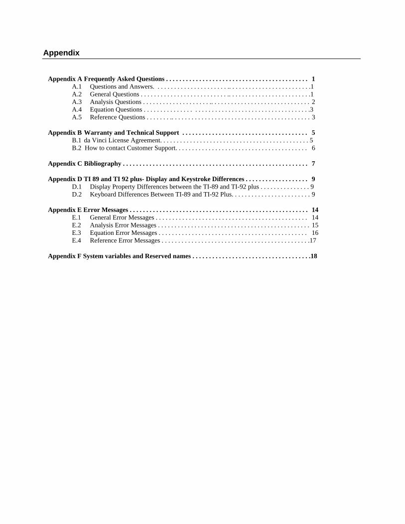
Appendix A Frequently Asked Questions . . . . . . . . . . . . . . . . . . . . . . . . . . . . . . . . . . . . . . . . . . . 1A.1 Questions and Answers. . . . . . . . . . . . . . . . . . . . . . .. . . . . . . . . . . . . . . . . . . . . . . . .1A.2 General Questions . . . . . . . . . . . . . . . . . . . . . . . . . . .. . . . . . . . . . . . . . . . . . . . . . . . .1A.3 Analysis Questions . . . . . . . . . . . . . . . . . . . . .. . . . . . . . . . . . . . . . . . . . . . . . . . . . . . 2A.4 Equation Questions . . . . . . . . . . . . . . . . . . . . . . . . . . . . . . . . . . . . . . . . . . . . . . . . . .3A.5 Reference Questions . . . . . . . .. . . . . . . . . . . . . . . . . . . . . . . . . . . . . . . . . . . . . . . . . . 3
Appendix B Warranty and Technical Support . . . . . . . . . . . . . . . . . . . . . . . . . . . . . . . . . . . . . . 5B.1 da Vinci License Agreement. . . . . . . . . . . . . . . . . . . . . . . . . . . . . . . . . . . . . . . . . . . . . 5B.2 How to contact Customer Support. . . . . . . . . . . . . . . . . . . . . . . . . . . . . . . . . . . . . . . . 6
Appendix C Bibliography . . . . . . . . . . . . . . . . . . . . . . . . . . . . . . . . . . . . . . . . . . . . . . . . . . . . . . . . 7
Appendix D TI 89 and TI 92 plus- Display and Keystroke Differences . . . . . . . . . . . . . . . . . . . 9D.1 Display Property Differences between the TI-89 and TI-92 plus . . . . . . . . . . . . . . . 9D.2 Keyboard Differences Between TI-89 and TI-92 Plus. . . . . . . . . . . . . . . . . . . . . . . . 9
Appendix E Error Messages . . . . . . . . . . . . . . . . . . . . . . . . . . . . . . . . . . . . . . . . . . . . . . . . . . . . . . 14E.1 General Error Messages . . . . . . . . . . . . . . . . . . . . . . . . . . . . . . . . . . . . . . . . . . . . . . 14E.2 Analysis Error Messages . . . . . . . . . . . . . . . . . . . . . . . . . . . . . . . . . . . . . . . . . . . . . . 15E.3 Equation Error Messages . . . . . . . . . . . . . . . . . . . . . . . . . . . . . . . . . . . . . . . . . . . . . 16E.4 Reference Error Messages . . . . . . . . . . . . . . . . . . . . . . . . . . . . . . . . . . . . . . . . . . . . .17
Appendix F System variables and Reserved names . . . . . . . . . . . . . . . . . . . . . . . . . . . . . . . . . . . .18
EE Pro for TI - 89, 92 PlusIntroduction to EE•Pro
i
Chapter 1 Introduction to EE•Pro
Thank you for your purchase of EE•Pro, a member of the PocketProfessional® Pro software series designed by daVinci Technologies to meet the computational needs of students and professionals in the engineering and scientificfields. Many long hours and late nights have been spent by the designers of this software to compile and organizethe subject material in this software. We hope you enjoy EE•Pro and that it serves as a valuable companion inyour electrical engineering career.
Topics in this chapter include:
• Key Features of EE•Pro• Download/Purchase Information• Manual Ordering• Memory Requirements
• Differences between the TI 89 and TI 92plus.
• Beginning EE•Pro• Manual Organization• Summary
1.1 Key Features of EE•Pro
The manual is organized into three sections representing the main menu headings of EE•Pro.
Analysis Equations ReferenceAC Circuits Resistive Circuits Resistor Color ChartPolyphase Circuits Capacitors and Electric Fields Standard Component ValuesLadder Network Inductors and Magnetism Semiconductor DataFilter Design Electron Motion Boolean ExpressionsGain and Frequency Meters and Bridges Boolean AlgebraFourier Transforms RL and RC Circuits TransformsTwo-Port Networks RLC Circuits ConstantsTransformer Calculations AC Circuits SI PrefixesTransmission Lines Polyphase CircuitsComputer Engineering Electrical ResonanceError Functions Operational Amplifier CircuitsCapital Budgeting Solid State Devices
Linear AmplifiersClass A, B, & C AmplifiersTransformersMotors and Generators
These main topic headings are further divided into sub-topics. A brief description of the main sections of thesoftware is listed below:
EE Pro for TI - 89, 92 PlusIntroduction to EE•Pro
ii
Analysis-(Chapters 2-14) Analysis is organized into 12 topics and 33 sub-topics. The tools in this sectionincorporate a wide variety of analysis methods used by electrical engineers. Examples include evaluation of ACcircuit performance characteristics, designing signal filters, building and computing ladder network properties,plotting transfer functions, estimating transformer and transmission line characteristics, performing binaryarithmetic operations, and estimating pay-back returns for different projects in capital budgeting. Many sectionsin analysis can perform calculations for numeric as well as symbolic entries. Equation Library (Chapters 15-31) This section contains over 700 equations organized under 16 topics and 105subtopics. In any sub-topic, the user is able to select a set of equations, enter known values and compute resultsfor unknown variables. The math engine is able to compute multiple or partial solution sets. A built-in unitmanagement feature allows for the entry and expression of values in SI or other established measurement systems.Descriptions of each variable, unit selection, and appropriate diagrams are included in this section of the software. Reference (Chapters 32-41) The Reference section of EE•Pro contains tables of information commonly found inelectrical engineering handbooks. Topics include physical and chemical properties of common semiconductormaterials, a list of fundamental constants commonly used by electrical engineers, tables of Fourier, Laplace, and z-transforms, and a list of Boolean algebraic expressions. Added features are the ability to perform simplecomputations, such as estimating standard (or preferred) manufacturer component values for inductors, resistors,and capacitors, in addition to a resistor color chart guide which can compute resistance and tolerance from aresistor’s color band sequence.
1.2 Purchasing, Downloading and Installing EE•Pro
The EE•Pro software can only be purchased on-line from the web store at Texas Instruments Inc. athttp://www.ti.com/calc. The software can be installed directly from your computer to your calculator using TI-GRAPH LINKTM hardware and software (sold separately). Directions for purchasing, downloading and installingEE•Pro software are available from TI’s website.
1.3 Manual Ordering Information
Chapters and Appendices of the manual for EE•Pro can be downloaded from TI’s web store and viewed using thefree Adobe Acrobat Reader which can be downloaded from http://www.adobe.com (it is recommended that you usethe latest version of the Acrobat reader and use the most updated driver for your printer). Printed manuals can bepurchased separately from da Vinci Technologies (see address on cover page or visit da Vinci’s websitehttp://www.dvtg.com/ticalcs/docs).
1.4 Memory Requirements
The EE•Pro program is installed in the system memory portion of the flash ROM, which is separate from theRAM available to the user. EE•Pro uses RAM to store some of its session information, including values enteredand computed by the user. The exact amount of memory required depends on the number of user-stored variablesand the number of session folders designated by the user. To view the available memory in your TI calculator, usethe ° function. It is recommended that at least 10K of free RAM be available for installation and use ofEE•Pro.
EE Pro for TI - 89, 92 PlusIntroduction to EE•Pro
iii
1.5 Differences between TI-89 and TI-92 plus
EE•Pro is designed for two models of graphing calculators from Texas Instruments, the TI-92 Plus and the TI-89.For consistency, keystrokes and symbols used in the manual are consistent with the TI-89. Equivalent key strokesfor the TI-92 plus are listed in Appendix D.
1.6 Beginning EE•Pro
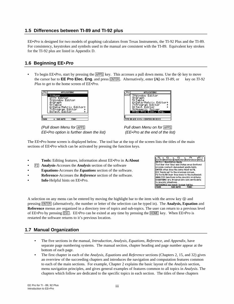
• To begin EE•Pro, start by pressing the O key. This accesses a pull down menu. Use the D key to movethe cursor bar to EE Pro Elec. Eng. and press ¸. Alternatively, enter [A] on TI-89, or Ñ key on TI-92Plus to get to the home screen of EE•Pro.
(Pull down Menu for O Pull down Menu on for O EE•Pro option is further down the list) (EE•Pro at the end of the list) The EE•Pro home screen is displayed below. The tool bar at the top of the screen lists the titles of the mainsections of EE•Pro which can be activated by pressing the function keys. • ƒ Tools: Editing features, information about EE•Pro in A:About• „ Analysis-Accesses the Analysis section of the software• … Equations-Accesses the Equations section of the software.• † Reference-Accesses the Reference section of the software.• ‡ Info-Helpful hints on EE•Pro. A selection on any menu can be entered by moving the highlight bar to the item with the arrow key D andpressing ¸ (alternatively, the number or letter of the selection can be typed in). The Analysis, Equation andReference menus are organized in a directory tree of topics and sub-topics. The user can return to a previous levelof EE•Pro by pressing N. EE•Pro can be exited at any time by pressing the " key. When EE•Pro isrestarted the software returns to it’s previous location.
1.7 Manual Organization
• The five sections in the manual, Introduction, Analysis, Equations, Reference, and Appendix, haveseparate page numbering systems. The manual section, chapter heading and page number appear at thebottom of each page.
• The first chapter in each of the Analysis, Equations and Reference sections (Chapters 2, 15, and 32) givesan overview of the succeeding chapters and introduces the navigation and computation features commonto each of the main sections. For example, Chapter 2 explains the basic layout of the Analysis section,menu navigation principles, and gives general examples of features common to all topics in Analysis. Thechapters which follow are dedicated to the specific topics in each section. The titles of these chapters
EE Pro for TI - 89, 92 PlusIntroduction to EE•Pro
iv
correspond to the topic headings in the software menus. The chapters list all the equations used andexplains their physical significance. These chapters also contain example problems and screen displays ofthe computed solutions.
• The Appendices contain trouble-shooting information, commonly asked questions, a bibliography used todevelop the software, and warranty information provided by Texas Instruments.
1.8 Manual Disclaimer
• The calculator screen displays in the manual were obtained during the testing stages of the software. Somescreen displays may appear slightly different due to final changes made in the software while the manual wasbeing completed.
1.9 Summary
The designers of EE•Pro have attempted to maintain the following features:• Easy-to-use, menu-based interface.• Computational efficiency for speed and performance.• Helpful-hints and context-sensitive information provided in the status line.• Advanced EE analysis routines, equations, and reference tables.• Comprehensive manual documentation for examples and quick reference.
We hope to continually add and refine the software products in the Pocket Professional series line. If you have anysuggestions for future releases or updates, please contact us via the da Vinci website http://www.dvtg.comor write to us at [email protected].
Best Regards,da Vinci Technologies Group, Inc.
EE Pro for TI - 89, 92 PlusAnalysis - Introduction to Analysis
1
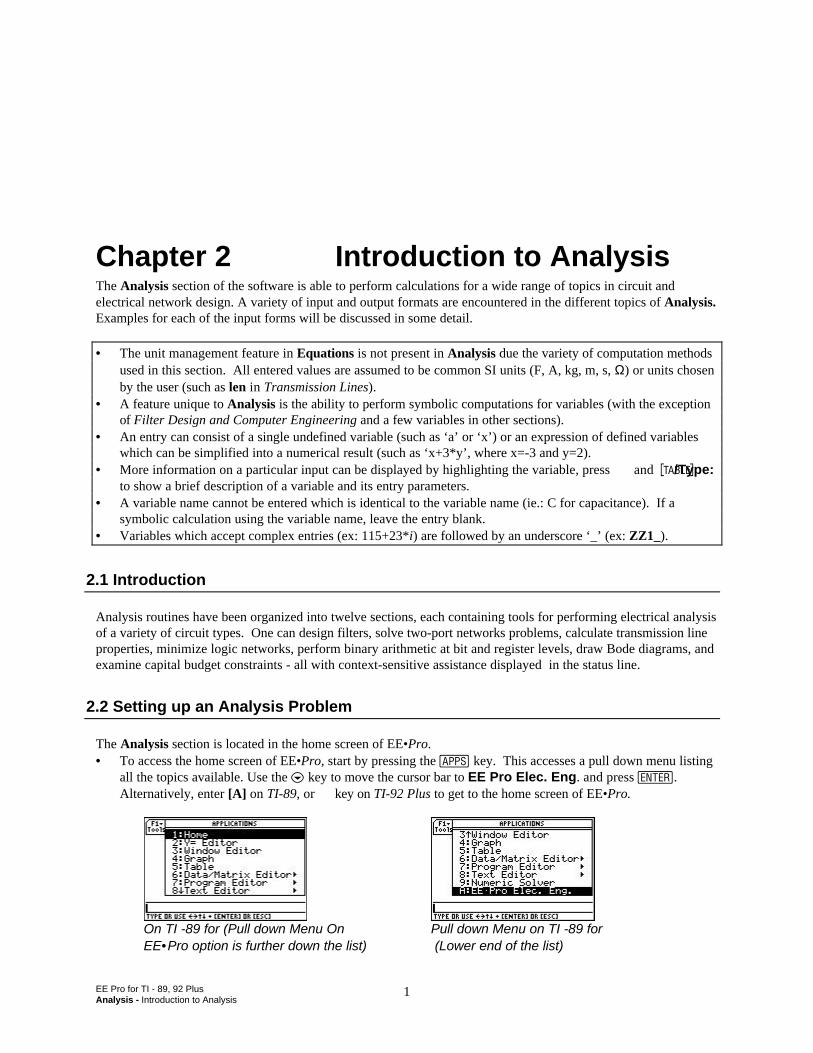
Chapter 2 Introduction to AnalysisThe Analysis section of the software is able to perform calculations for a wide range of topics in circuit andelectrical network design. A variety of input and output formats are encountered in the different topics of Analysis.Examples for each of the input forms will be discussed in some detail.
• The unit management feature in Equations is not present in Analysis due the variety of computation methodsused in this section. All entered values are assumed to be common SI units (F, A, kg, m, s, Ω) or units chosenby the user (such as len in Transmission Lines).
• A feature unique to Analysis is the ability to perform symbolic computations for variables (with the exceptionof Filter Design and Computer Engineering and a few variables in other sections).
• An entry can consist of a single undefined variable (such as ‘a’ or ‘x’) or an expression of defined variableswhich can be simplified into a numerical result (such as ‘x+3*y’, where x=-3 and y=2).
• More information on a particular input can be displayed by highlighting the variable, press ‡ and ©/Type:to show a brief description of a variable and its entry parameters.
• A variable name cannot be entered which is identical to the variable name (ie.: C for capacitance). If asymbolic calculation using the variable name, leave the entry blank.
• Variables which accept complex entries (ex: 115+23*i) are followed by an underscore ‘_’ (ex: ZZ1_).
2.1 Introduction
Analysis routines have been organized into twelve sections, each containing tools for performing electrical analysisof a variety of circuit types. One can design filters, solve two-port networks problems, calculate transmission lineproperties, minimize logic networks, perform binary arithmetic at bit and register levels, draw Bode diagrams, andexamine capital budget constraints - all with context-sensitive assistance displayed in the status line.
2.2 Setting up an Analysis Problem
The Analysis section is located in the home screen of EE•Pro.• To access the home screen of EE•Pro, start by pressing the O key. This accesses a pull down menu listing
all the topics available. Use the D key to move the cursor bar to EE Pro Elec. Eng. and press ¸.Alternatively, enter [A] on TI-89, or Ñ key on TI-92 Plus to get to the home screen of EE•Pro.
On TI -89 for (Pull down Menu On Pull down Menu on TI -89 for EE•Pro option is further down the list) (Lower end of the list)
EE Pro for TI - 89, 92 PlusAnalysis - Introduction to Analysis
2
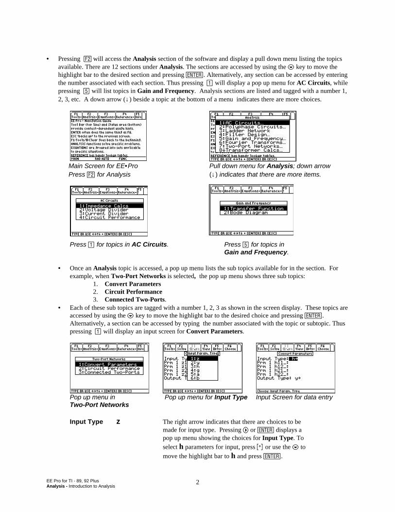
• Pressing „ will access the Analysis section of the software and display a pull down menu listing the topicsavailable. There are 12 sections under Analysis. The sections are accessed by using the D key to move thehighlight bar to the desired section and pressing ¸. Alternatively, any section can be accessed by enteringthe number associated with each section. Thus pressing ¨ will display a pop up menu for AC Circuits, whilepressing z will list topics in Gain and Frequency. Analysis sections are listed and tagged with a number 1,2, 3, etc. A down arrow (↓) beside a topic at the bottom of a menu indicates there are more choices.
Main Screen for EE•Pro Pull down menu for Analysis; down arrow Press „ for Analysis (↓) indicates that there are more items.
Press ¨ for topics in AC Circuits. Press z for topics in Gain and Frequency.
• Once an Analysis topic is accessed, a pop up menu lists the sub topics available for in the section. Forexample, when Two-Port Networks is selected, the pop up menu shows three sub topics:
1. Convert Parameters2. Circuit Performance3. Connected Two-Ports.
• Each of these sub topics are tagged with a number 1, 2, 3 as shown in the screen display. These topics areaccessed by using the D key to move the highlight bar to the desired choice and pressing ¸.Alternatively, a section can be accessed by typing the number associated with the topic or subtopic. Thuspressing ¨ will display an input screen for Convert Parameters.
Pop up menu in Pop up menu for Input Type Input Screen for data entryTwo-Port Networks
Input Type z The right arrow indicates that there are choices to bemade for input type. Pressing B or ¸ displays apop up menu showing the choices for Input Type. Toselect h parameters for input, press ª or use the D tomove the highlight bar to h and press ¸.
EE Pro for TI - 89, 92 PlusAnalysis - Introduction to Analysis
3
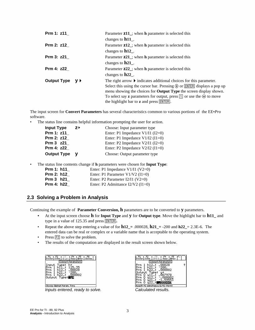
Prm 1: z11_ Parameter z11_; when h parameter is selected thischanges to h11_.
Prm 2: z12_ Parameter z12_; when h parameter is selected thischanges to h12_.
Prm 3: z21_ Parameter z21_; when h parameter is selected thischanges to h21_.
Prm 4: z22_ Parameter z22_; when h parameter is selected thischanges to h22_.
Output Type y44 The right arrow44indicates additional choices for this parameter. Select this using the cursor bar. Pressing B or ¸ displays a pop upmenu showing the choices for Output Type the screen display shown.To select say z parameters for output, press ¨ or use the D to movethe highlight bar to z and press ¸.
The input screen for Convert Parameters has several characteristics common to various portions of the EE•Prosoftware.• The status line contains helpful information prompting the user for action.
Input Type z! Choose: Input parameter typePrm 1: z11_ Enter: P1 Impedance V1/I1 (I2=0)Prm 2: z12_ Enter: P1 Impedance V1/I2 (I1=0)Prm 3 z21_ Enter: P2 Impedance V2/I1 (I2=0)Prm 4: z22_ Enter: P2 Impedance V2/I2 (I1=0)Output Type y Choose: Output parameter type
• The status line contents change if h parameters were chosen for Input Type:Prm 1: h11_ Enter: P1 Impedance V1/I1 (V2=0)Prm 2: h12_ Enter: P1 Parameter V1/V2 (I1=0)Prm 3 h21_ Enter: P2 Parameter I2/I1 (V2=0)Prm 4: h22_ Enter: P2 Admittance I2/V2 (I1=0)
2.3 Solving a Problem in Analysis
Continuing the example of Parameter Conversion, h parameters are to be converted to y parameters.• • At the input screen choose h for Input Type and y for Output type. Move the highlight bar to h11_ and
type in a value of 125.35 and press ¸.• Repeat the above step entering a value of for h12_= .000028, h21_= -200 and h22_= 2.3E-6. The
entered data can be real or complex or a variable name that is acceptable to the operating system.• Press „ to solve the problem.• The results of the computation are displayed in the result screen shown below.
Inputs entered, ready to solve. Calculated results.
EE Pro for TI - 89, 92 PlusAnalysis - Introduction to Analysis
4
Note: If the calculator is turned off automatically or manually while a results screen is being displayed, whenEE•Pro is accessed again via the O key, the software automatically bypasses the home screen of EE•Pro andreturns to the screen result display.
2.4 Special Function Keys in Analysis Routines
When Analysis functions are selected, the function keys in the tool bar access or activate features which arespecific to the context of the section. They are listed in Table 2-1:
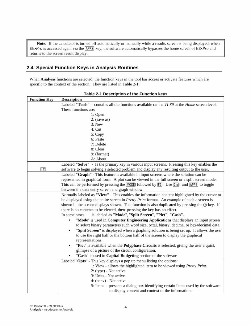
Table 2-1 Description of the Function keysFunction Key Description
ƒ
Labeled "Tools" - contains all the functions available on the TI-89 at the Home screen level.These functions are:
1: Open2: (save as)3: New4: Cut5: Copy6: Paste7: Delete8: Clear9: (format)A: About
„
Labeled "Solve" - Is the primary key in various input screens. Pressing this key enables thesoftware to begin solving a selected problem and display any resulting output to the user.
…
Labeled "Graph" - This feature is available in input screens where the solution can berepresented in graphical form. A plot can be viewed in the full screen or a split screen mode.This can be performed by pressing the 3 followed by „. Use 2 and O to togglebetween the data entry screen and graph window.
†
Normally labeled as "View" - This enables the information content highlighted by the cursor tobe displayed using the entire screen in Pretty Print format. An example of such a screen isshown in the screen displays shown. This function is also duplicated by pressing the B key. Ifthere is no contents to be viewed, then pressing the key has no effect.In some cases † is labeled as "Mode", "Split Screen", "Pict", "Cash".
• "Mode" is used in Computer Engineering Applications that displays an input screento select binary parameters such word size, octal, binary, decimal or hexadecimal data.
• "Split Screen" is displayed when a graphing solution is being set up. It allows the userto use the right half or the bottom half of the screen to display the graphicalrepresentations.
• "Pict" is available when the Polyphase Circuits is selected, giving the user a quickglimpse of a picture of the circuit configuration.
• "Cash" is used in Capital Budgeting section of the software
‡
Labeled "Opts" - This key displays a pop up menu listing the options:1: View - allows the highlighted item to be viewed using Pretty Print.2: (type) - Not active3: Units - Not active4: (conv) - Not active5: Icons - presents a dialog box identifying certain Icons used by the software to display content and context of the information.
EE Pro for TI - 89, 92 PlusAnalysis - Introduction to Analysis
5
6: (know)- Not active7: Want - Not active
ˆ
• “Edit” - Brings in a data entry line for the highlighted parameter.• “Choose” in Capital Budgeting enabling the user to select from one of nine projects.• “√√ Check” requesting the user to press this key to select a highlighted parameter for use in
an Analysis computation.
‰
Appears only when solving problems in the Ladder Network section and is labeled "Add"; thisdisplays the input screen allowing the user to add new elements to a ladder network.
Š
Appears only when solving problems in the Ladder Network Section and is labeled "Del".Pressing † will delete an element from the ladder network.
2.5 Data Fields Analysis Functions and Sample Problems
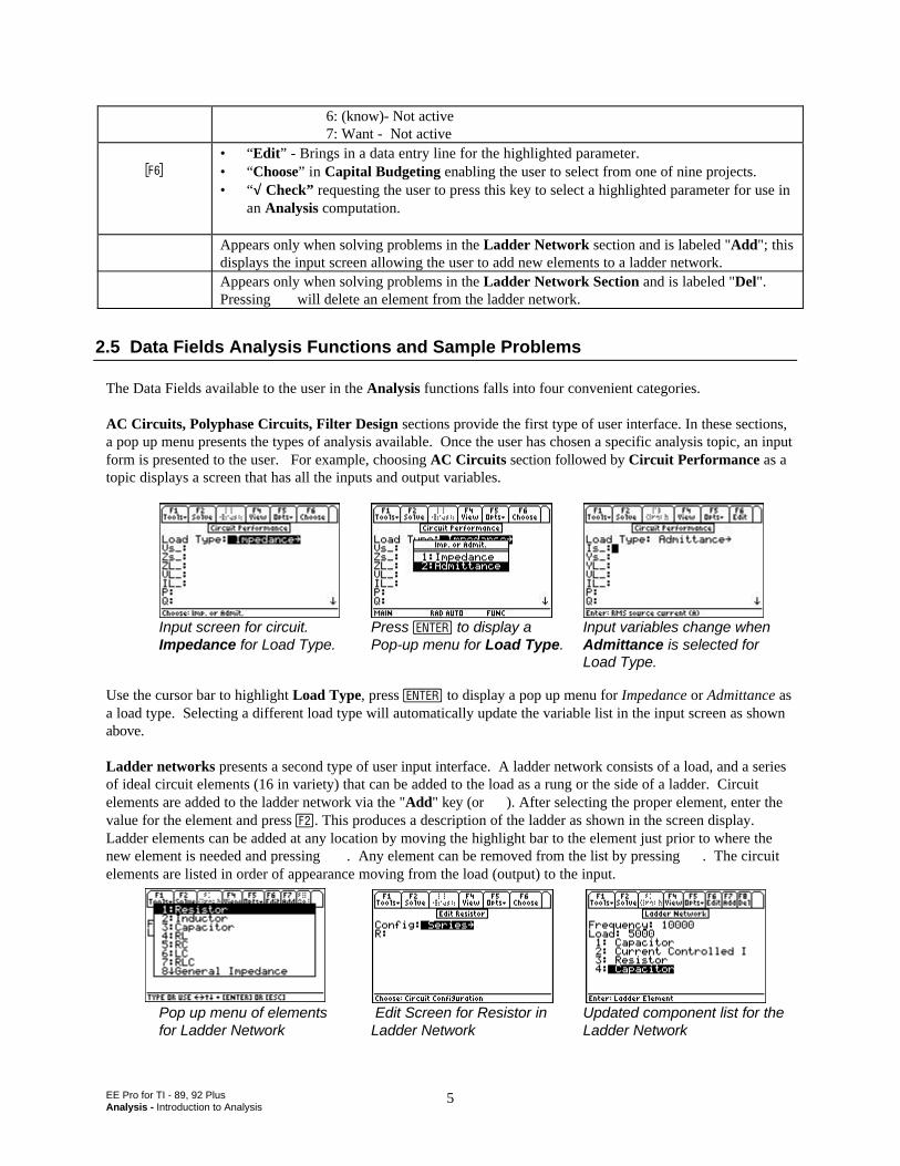
The Data Fields available to the user in the Analysis functions falls into four convenient categories.
AC Circuits, Polyphase Circuits, Filter Design sections provide the first type of user interface. In these sections,a pop up menu presents the types of analysis available. Once the user has chosen a specific analysis topic, an inputform is presented to the user. For example, choosing AC Circuits section followed by Circuit Performance as atopic displays a screen that has all the inputs and output variables.
Input screen for circuit. Press ¸ to display a Input variables change whenImpedance for Load Type. Pop-up menu for Load Type. Admittance is selected for
Load Type.
Use the cursor bar to highlight Load Type, press ¸ to display a pop up menu for Impedance or Admittance asa load type. Selecting a different load type will automatically update the variable list in the input screen as shownabove.
Ladder networks presents a second type of user input interface. A ladder network consists of a load, and a seriesof ideal circuit elements (16 in variety) that can be added to the load as a rung or the side of a ladder. Circuitelements are added to the ladder network via the "Add" key (or ‰). After selecting the proper element, enter thevalue for the element and press „. This produces a description of the ladder as shown in the screen display.Ladder elements can be added at any location by moving the highlight bar to the element just prior to where thenew element is needed and pressing ‰. Any element can be removed from the list by pressing Š. The circuitelements are listed in order of appearance moving from the load (output) to the input.
Pop up menu of elements Edit Screen for Resistor in Updated component list for thefor Ladder Network Ladder Network Ladder Network
EE Pro for TI - 89, 92 Plus 5Analysis - Introduction to Analysis
51
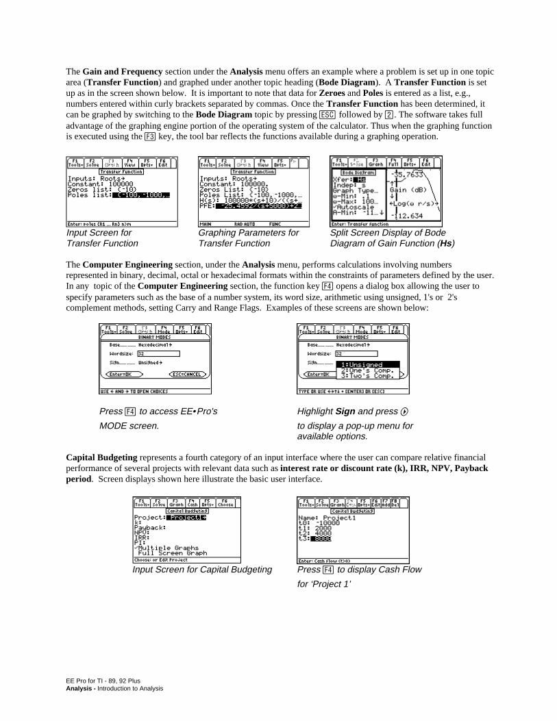
The Gain and Frequency section under the Analysis menu offers an example where a problem is set up in one topicarea (Transfer Function) and graphed under another topic heading (Bode Diagram). A Transfer Function is setup as in the screen shown below. It is important to note that data for Zeroes and Poles is entered as a list, e.g.,numbers entered within curly brackets separated by commas. Once the Transfer Function has been determined, itcan be graphed by switching to the Bode Diagram topic by pressing N followed by ©. The software takes fulladvantage of the graphing engine portion of the operating system of the calculator. Thus when the graphing functionis executed using the … key, the tool bar reflects the functions available during a graphing operation.
Input Screen for Graphing Parameters for Split Screen Display of BodeTransfer Function Transfer Function Diagram of Gain Function (Hs)
The Computer Engineering section, under the Analysis menu, performs calculations involving numbersrepresented in binary, decimal, octal or hexadecimal formats within the constraints of parameters defined by the user.In any topic of the Computer Engineering section, the function key † opens a dialog box allowing the user tospecify parameters such as the base of a number system, its word size, arithmetic using unsigned, 1's or 2'scomplement methods, setting Carry and Range Flags. Examples of these screens are shown below:
Press † to access EE•Pro's Highlight Sign and press B
MODE screen. to display a pop-up menu for available options.
Capital Budgeting represents a fourth category of an input interface where the user can compare relative financialperformance of several projects with relevant data such as interest rate or discount rate (k), IRR, NPV, Paybackperiod. Screen displays shown here illustrate the basic user interface.
Input Screen for Capital Budgeting Press † to display Cash Flow
for ‘Project 1’
EE Pro for TI - 89, 92 PlusAnalysis - Introduction to Analysis
7
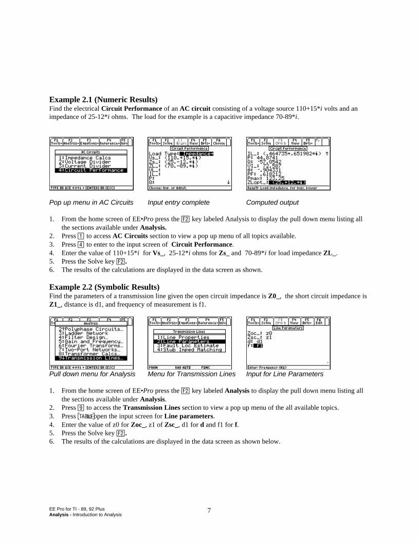
Example 2.1 (Numeric Results)Find the electrical Circuit Performance of an AC circuit consisting of a voltage source 110+15*i volts and animpedance of 25-12*i ohms. The load for the example is a capacitive impedance 70-89*i.
Pop up menu in AC Circuits Input entry complete Computed output
1. From the home screen of EE•Pro press the „ key labeled Analysis to display the pull down menu listing allthe sections available under Analysis.
2. Press ¨ to access AC Circuits section to view a pop up menu of all topics available.3. Press y to enter to the input screen of Circuit Performance.4. Enter the value of 110+15*i for Vs_, 25-12*i ohms for Zs_ and 70-89*i for load impedance ZL_.5. Press the Solve key „.6. The results of the calculations are displayed in the data screen as shown.
Example 2.2 (Symbolic Results)Find the parameters of a transmission line given the open circuit impedance is Z0_, the short circuit impedance isZ1_, distance is d1, and frequency of measurement is f1.
Pull down menu for Analysis Menu for Transmission Lines Input for Line Parameters
1. From the home screen of EE•Pro press the „ key labeled Analysis to display the pull down menu listing allthe sections available under Analysis.
2. Press o to access the Transmission Lines section to view a pop up menu of the all available topics.3. Press © to open the input screen for Line parameters.4. Enter the value of z0 for Zoc_, z1 of Zsc_, d1 for d and f1 for f.5. Press the Solve key „.6. The results of the calculations are displayed in the data screen as shown below.
EE Pro for TI - 89, 92 PlusAnalysis - Introduction to Analysis
8
Input entered symbolically Calculated Output also symbolic
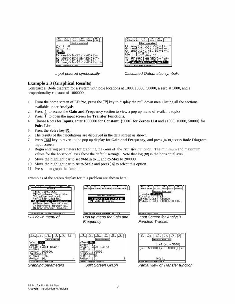
Example 2.3 (Graphical Results)Construct a Bode diagram for a system with pole locations at 1000, 10000, 50000, a zero at 5000, and aproportionality constant of 1000000.
1. From the home screen of EE•Pro, press the „ key to display the pull down menu listing all the sectionsavailable under Analysis.
2. Press z to access the Gain and Frequency section to view a pop up menu of available topics.3. Press ¨ to open the input screen for Transfer Functions.4. Choose Roots for Inputs, enter 1000000 for Constant, 5000 for Zeroes List and 1000, 10000, 50000 for
Poles List.5. Press the Solve key „.6. The results of the calculations are displayed in the data screen as shown.7. Press N key to revert to the pop up display for Gain and Frequency, and press © to access Bode Diagram
input screen.8. Begin entering parameters for graphing the Gain of the Transfer Function. The minimum and maximum
values for the horizontal axis show the default settings. Note that log (ω) is the horizontal axis.9. Move the highlight bar to set ω-Min to 1, and ω-Max to 200000.10. Move the highlight bar to Auto Scale and press ˆ to select this option.11. Press …to graph the function.
Examples of the screen display for this problem are shown here:
Pull down menu of Pop up menu for Gain and Input Screen for Analysis Frequency Function Transfer
Graphing parameters Split Screen Graph Partial view of Transfer function

EE Pro for TI - 89, 92 PlusAnalysis - Introduction to Analysis
9
2.6 Session Folders, Variable Names
EE•Pro automatically stores its variables in the current folder specified by the user in 3 or the HOME screens.The current folder name is displayed in the lower left corner of the screen (default is “Main”). To create a newfolder to store values for a particular session of EE•Pro, press ƒ:/TOOLS, ª:/NEW and type the name of thenew folder (see Chapter 5 of the TI-89 Guidebook for the complete details of creating and managing folders). There are several ways to display or recall a value:
• The contents of variables in any folder can be displayed using the °, moving the cursor to thevariable name and pressing ˆ to display the contents of a particular variable.
• Variables in a current folder can be recalled in the HOME screen by typing the variable name.• Finally, values and units can be copied and recalled using the ƒ/Tools 5:COPY and 6:PASTE
feature.
All inputs and calculated results from Analysis and Equations section are saved as variable names. Previouslycalculated, or entered values for variables in a folder are replaced when equations are solved using new values forinputs.
Overwriting of variable values in graphingWhen an equation or analysis function is graphed, EE•Pro creates a function for the TI grapher which expressesthe dependent variable in terms of the independent variable. This function is stored under the variable namepro(x). When the EE•Pro’s equation grapher is executed, values are inserted into the independent variable forpro(x) and values for the dependent value are calculated. Whatever values which previously existed in either ofthe dependent and independent variables in the current folder are cleared. To preserve data under variablenames which may conflict with EE•Pro’s variables, run EE•Pro in a separate folder.
Reserved VariablesThere is a list of reserved variable names used by the TI operating system which cannot be used as user variablenames or entries. These reserved variables are listed in Appendix F.
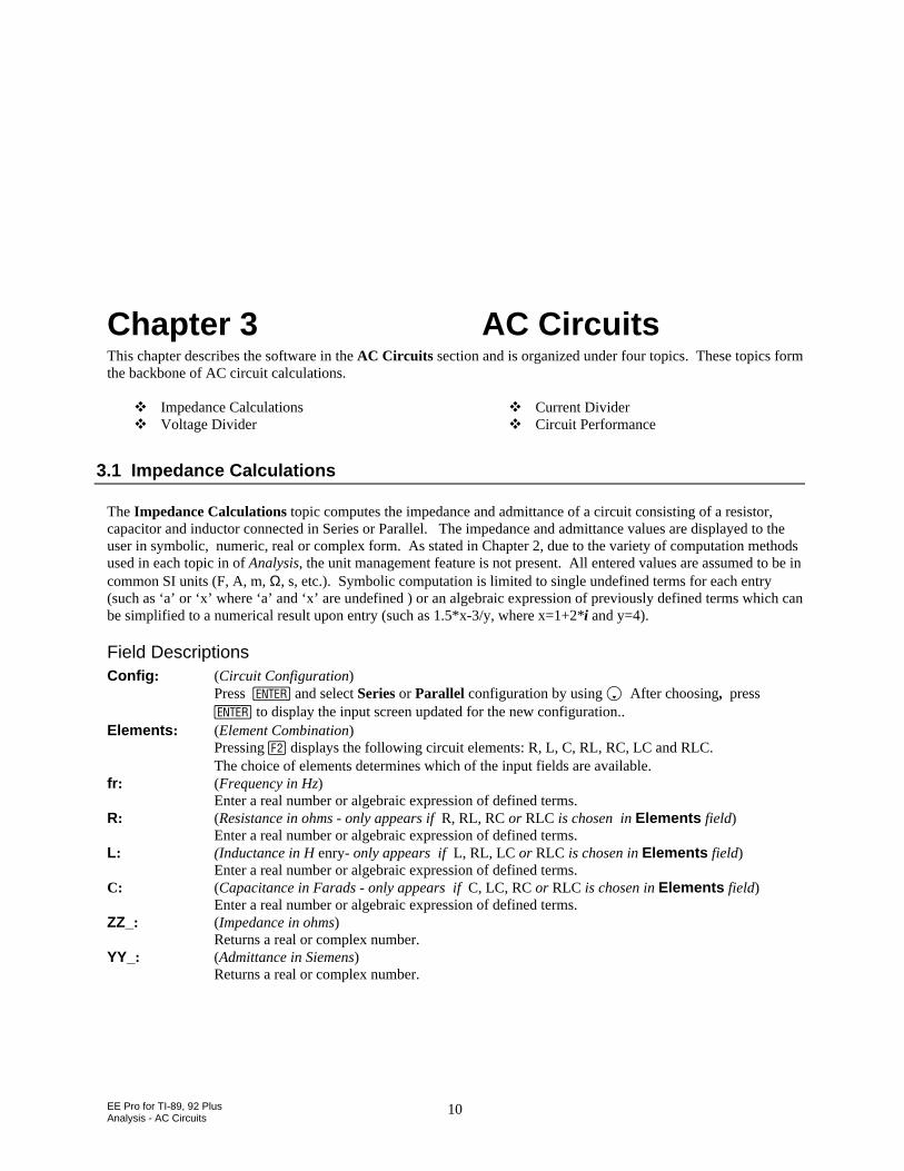
EE Pro for TI-89, 92 PlusAnalysis - AC Circuits
10
Chapter 3 AC CircuitsThis chapter describes the software in the AC Circuits section and is organized under four topics. These topics formthe backbone of AC circuit calculations.
Impedance CalculationsVoltage Divider
Current DividerCircuit Performance
3.1 Impedance Calculations
The Impedance Calculations topic computes the impedance and admittance of a circuit consisting of a resistor,capacitor and inductor connected in Series or Parallel. The impedance and admittance values are displayed to theuser in symbolic, numeric, real or complex form. As stated in Chapter 2, due to the variety of computation methodsused in each topic in of Analysis, the unit management feature is not present. All entered values are assumed to be incommon SI units (F, A, m, Ω, s, etc.). Symbolic computation is limited to single undefined terms for each entry(such as ‘a’ or ‘x’ where ‘a’ and ‘x’ are undefined ) or an algebraic expression of previously defined terms which canbe simplified to a numerical result upon entry (such as 1.5*x-3/y, where x=1+2*i and y=4).
Field DescriptionsConfig : (Circuit Configuration)
Press and select Series or Parallel configuration by using D After choosing, press¸ to display the input screen updated for the new configuration..
Elements : (Element Combination)Pressing „ displays the following circuit elements: R, L, C, RL, RC, LC and RLC.The choice of elements determines which of the input fields are available.
fr : (Frequency in Hz) Enter a real number or algebraic expression of defined terms.
R: (Resistance in ohms - only appears if R, RL, RC or RLC is chosen in Elements field)Enter a real number or algebraic expression of defined terms.
L: (Inductance in H enry- only appears if L, RL, LC or RLC is chosen in Elements field) Enter a real number or algebraic expression of defined terms.
C: (Capacitance in Farads - only appears if C, LC, RC or RLC is chosen in Elements field)Enter a real number or algebraic expression of defined terms.
ZZ_: (Impedance in ohms)Returns a real or complex number.
YY_: (Admittance in Siemens)Returns a real or complex number.
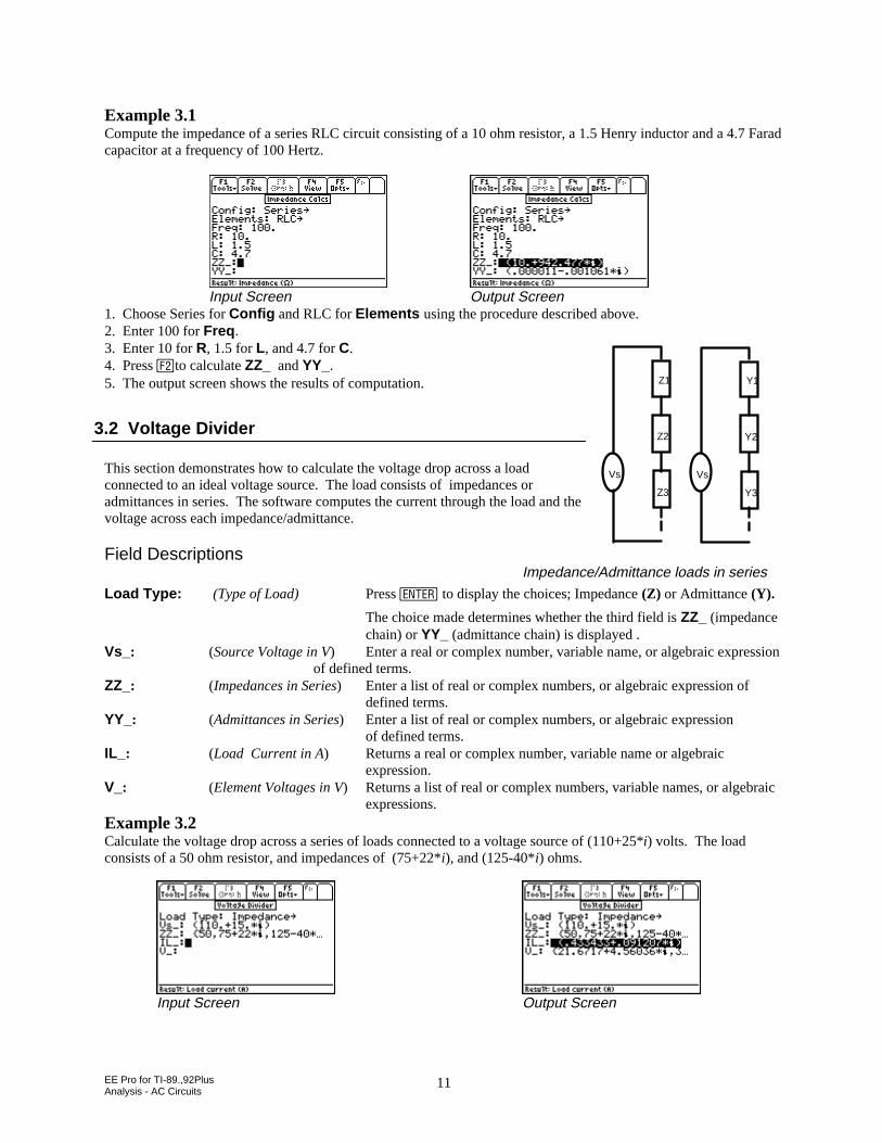
EE Pro for TI-89.,92PlusAnalysis - AC Circuits
11
Example 3.1 Compute the impedance of a series RLC circuit consisting of a 10 ohm resistor, a 1.5 Henry inductor and a 4.7 Faradcapacitor at a frequency of 100 Hertz.
Input Screen Output Screen1. Choose Series for Config and RLC for Elements using the procedure described above.2. Enter 100 for Freq .3. Enter 10 for R, 1.5 for L, and 4.7 for C.4. Press „to calculate ZZ_ and YY_.5. The output screen shows the results of computation.
3.2 Voltage Divider
This section demonstrates how to calculate the voltage drop across a loadconnected to an ideal voltage source. The load consists of impedances oradmittances in series. The software computes the current through the load and thevoltage across each impedance/admittance.
Field DescriptionsImpedance/Admittance loads in series
Load Type: (Type of Load) Press to display the choices; Impedance (Z) or Admittance (Y).
The choice made determines whether the third field is ZZ_ (impedancechain) or YY_ (admittance chain) is displayed .
Vs_: (Source Voltage in V) Enter a real or complex number, variable name, or algebraic expression of defined terms.
ZZ_: (Impedances in Series) Enter a list of real or complex numbers, or algebraic expression of defined terms.
YY_: (Admittances in Series) Enter a list of real or complex numbers, or algebraic expressionof defined terms.
IL_: (Load Current in A) Returns a real or complex number, variable name or algebraicexpression.
V_: (Element Voltages in V) Returns a list of real or complex numbers, variable names, or algebraicexpressions.
Example 3.2 Calculate the voltage drop across a series of loads connected to a voltage source of (110+25*i) volts. The loadconsists of a 50 ohm resistor, and impedances of (75+22*i), and (125-40*i) ohms.
Input Screen Output Screen
Vs
Y1
Y2
Y3
Vs
Z1
Z2
Z3
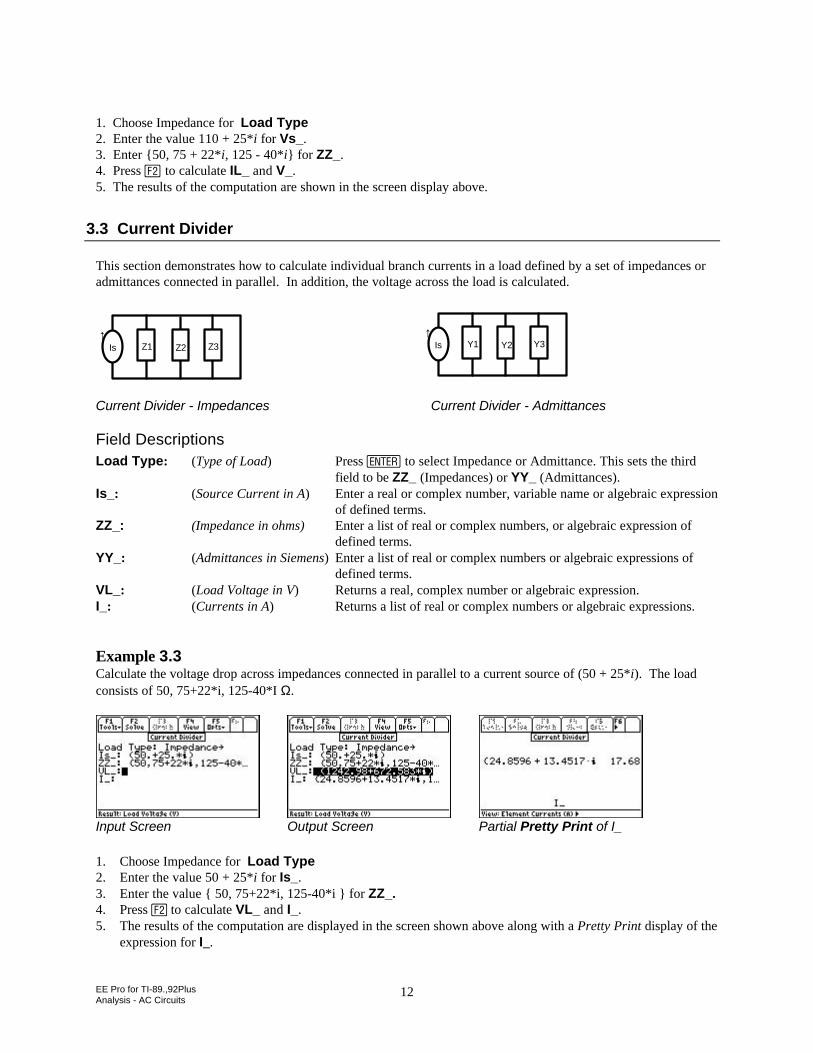
EE Pro for TI-89.,92PlusAnalysis - AC Circuits
12
1. Choose Impedance for Load Type 2. Enter the value 110 + 25*i for Vs_.3. Enter 50, 75 + 22*i, 125 - 40*i for ZZ_.4. Press „ to calculate IL_ and V_.5. The results of the computation are shown in the screen display above.
3.3 Current Divider
This section demonstrates how to calculate individual branch currents in a load defined by a set of impedances oradmittances connected in parallel. In addition, the voltage across the load is calculated.
Current Divider - Impedances Current Divider - Admittances
Field DescriptionsLoad Type: (Type of Load) Press ¸ to select Impedance or Admittance. This sets the third
field to be ZZ_ (Impedances) or YY_ (Admittances).Is_: (Source Current in A) Enter a real or complex number, variable name or algebraic expression
of defined terms.ZZ_: (Impedance in ohms) Enter a list of real or complex numbers, or algebraic expression of
defined terms.YY_: (Admittances in Siemens) Enter a list of real or complex numbers or algebraic expressions of
defined terms.VL_: (Load Voltage in V) Returns a real, complex number or algebraic expression.I_: (Currents in A) Returns a list of real or complex numbers or algebraic expressions.
Example 3.3Calculate the voltage drop across impedances connected in parallel to a current source of (50 + 25*i). The loadconsists of 50, 75+22*i, 125-40*I Ω.
Input Screen Output Screen Partial Pretty Print of I_
1. Choose Impedance for Load Type 2. Enter the value 50 + 25*i for Is_.3. Enter the value 50, 75+22*i, 125-40*i for ZZ_.4. Press „ to calculate VL_ and I_.5. The results of the computation are displayed in the screen shown above along with a Pretty Print display of the
expression for I_.
↑Is Z1 Z2 Z3
↑Is Y1 Y2 Y3
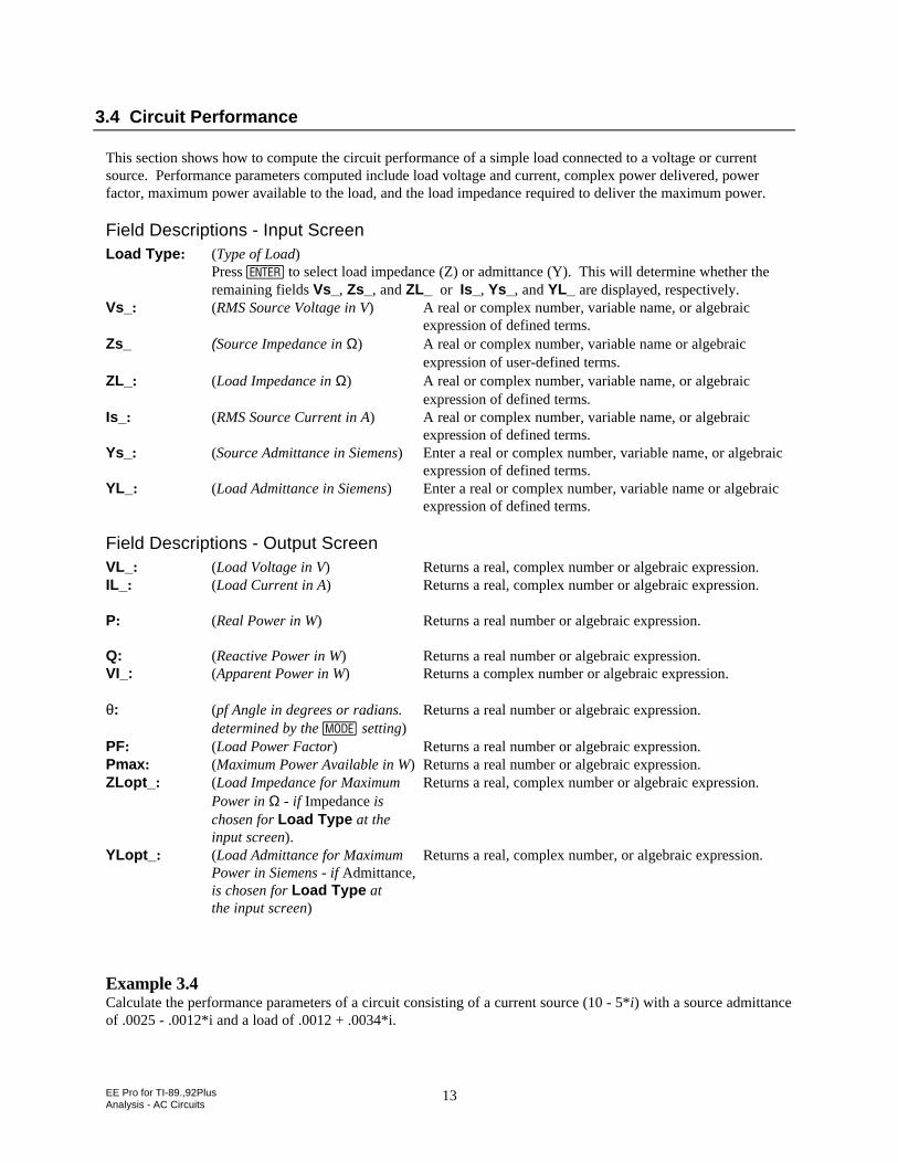
EE Pro for TI-89.,92PlusAnalysis - AC Circuits
13
3.4 Circuit Performance
This section shows how to compute the circuit performance of a simple load connected to a voltage or currentsource. Performance parameters computed include load voltage and current, complex power delivered, powerfactor, maximum power available to the load, and the load impedance required to deliver the maximum power.
Field Descriptions - Input ScreenLoad Type: (Type of Load)
Press ¸ to select load impedance (Z) or admittance (Y). This will determine whether theremaining fields Vs_, Zs_, and ZL_ or Is_, Ys_, and YL_ are displayed, respectively.
Vs_: (RMS Source Voltage in V) A real or complex number, variable name, or algebraicexpression of defined terms.
Zs_ (Source Impedance in Ω) A real or complex number, variable name or algebraicexpression of user-defined terms.
ZL_: (Load Impedance in Ω) A real or complex number, variable name, or algebraicexpression of defined terms.
Is_: (RMS Source Current in A) A real or complex number, variable name, or algebraicexpression of defined terms.
Ys_: (Source Admittance in Siemens) Enter a real or complex number, variable name, or algebraicexpression of defined terms.
YL_: (Load Admittance in Siemens) Enter a real or complex number, variable name or algebraicexpression of defined terms.
Field Descriptions - Output ScreenVL_: (Load Voltage in V) Returns a real, complex number or algebraic expression.IL_: (Load Current in A) Returns a real, complex number or algebraic expression.
P: (Real Power in W) Returns a real number or algebraic expression.
Q: (Reactive Power in W) Returns a real number or algebraic expression.VI_: (Apparent Power in W) Returns a complex number or algebraic expression.
θ: (pf Angle in degrees or radians. Returns a real number or algebraic expression.determined by the 3 setting)
PF: (Load Power Factor) Returns a real number or algebraic expression.Pmax: (Maximum Power Available in W) Returns a real number or algebraic expression.ZLopt_: (Load Impedance for Maximum Returns a real, complex number or algebraic expression.
Power in Ω - if Impedance ischosen for Load Type at theinput screen).
YLopt_: (Load Admittance for Maximum Returns a real, complex number, or algebraic expression.Power in Siemens - if Admittance, is chosen for Load Type atthe input screen)
Example 3.4 Calculate the performance parameters of a circuit consisting of a current source (10 - 5*i) with a source admittanceof .0025 - .0012*i and a load of .0012 + .0034*i.
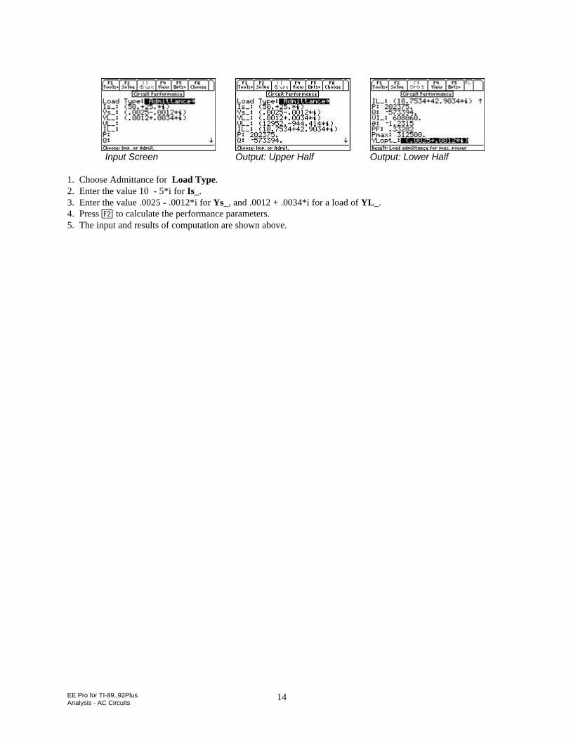
EE Pro for TI-89.,92PlusAnalysis - AC Circuits
14
Input Screen Output: Upper Half Output: Lower Half
1. Choose Admittance for Load Type.2. Enter the value 10 - 5*i for Is_.3. Enter the value .0025 - .0012*i for Ys_, and .0012 + .0034*i for a load of YL_.4. Press „ to calculate the performance parameters.5. The input and results of computation are shown above.
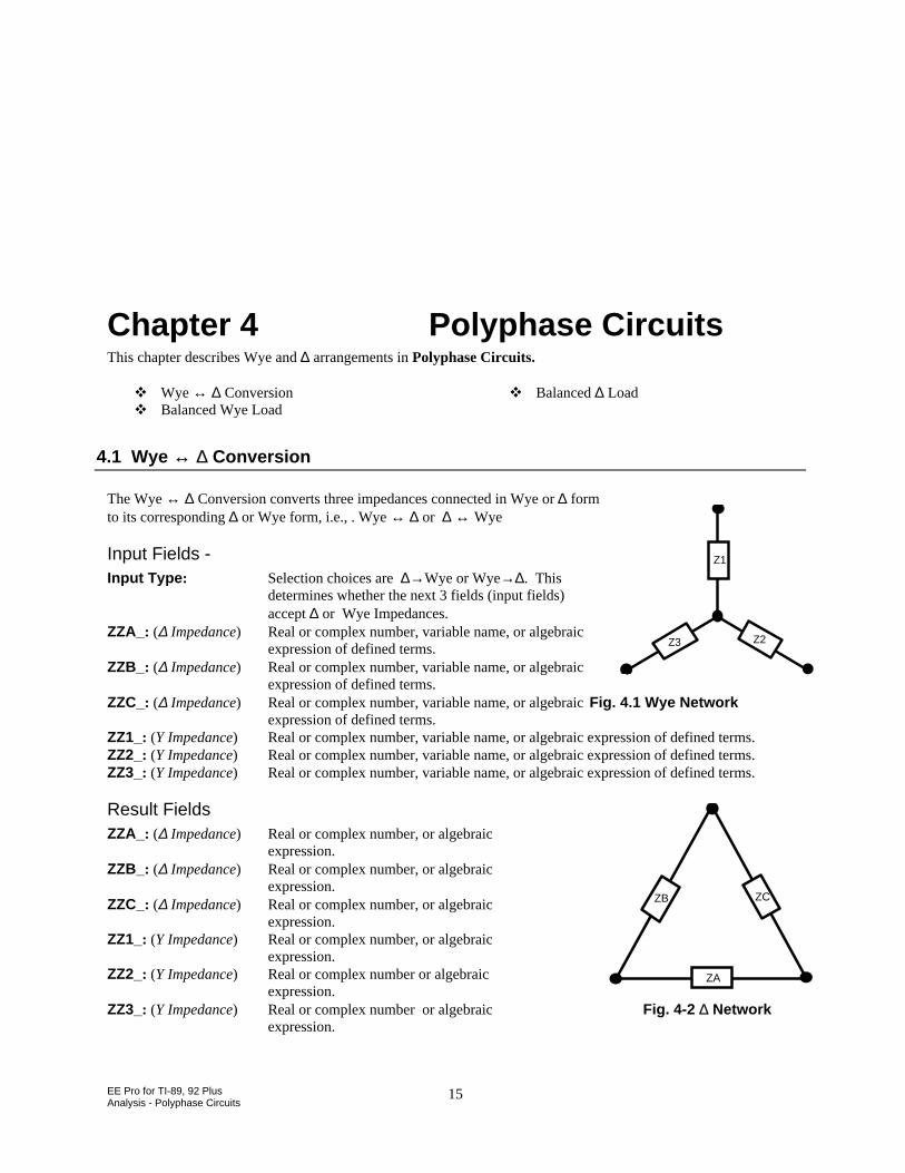
EE Pro for TI-89, 92 PlusAnalysis - Polyphase Circuits
15
Chapter 4 Polyphase CircuitsThis chapter describes Wye and ∆ arrangements in Polyphase Circuits.
Wye ↔ ∆ ConversionBalanced Wye Load
Balanced ∆ Load
4.1 Wye ↔ ∆ Conversion
The Wye ↔ ∆ Conversion converts three impedances connected in Wye or ∆ formto its corresponding ∆ or Wye form, i.e., . Wye ↔ ∆ or ∆ ↔ Wye
Input Fields -Input Type : Selection choices are ∆→Wye or Wye→∆. This
determines whether the next 3 fields (input fields)accept ∆ or Wye Impedances.
ZZA_: (∆ Impedance) Real or complex number, variable name, or algebraicexpression of defined terms.
ZZB_: (∆ Impedance) Real or complex number, variable name, or algebraicexpression of defined terms.
ZZC_: (∆ Impedance) Real or complex number, variable name, or algebraic Fig. 4.1 Wye Networkexpression of defined terms.
ZZ1_: (Y Impedance) Real or complex number, variable name, or algebraic expression of defined terms.ZZ2_: (Y Impedance) Real or complex number, variable name, or algebraic expression of defined terms.ZZ3_: (Y Impedance) Real or complex number, variable name, or algebraic expression of defined terms.
Result FieldsZZA_: (∆ Impedance) Real or complex number, or algebraic
expression.ZZB_: (∆ Impedance) Real or complex number, or algebraic
expression.ZZC_: (∆ Impedance) Real or complex number, or algebraic
expression.ZZ1_: (Y Impedance) Real or complex number, or algebraic
expression.ZZ2_: (Y Impedance) Real or complex number or algebraic
expression.ZZ3_: (Y Impedance) Real or complex number or algebraic Fig. 4-2 ∆ Network
expression.
Z1
Z3 Z2
ZA
ZCZB
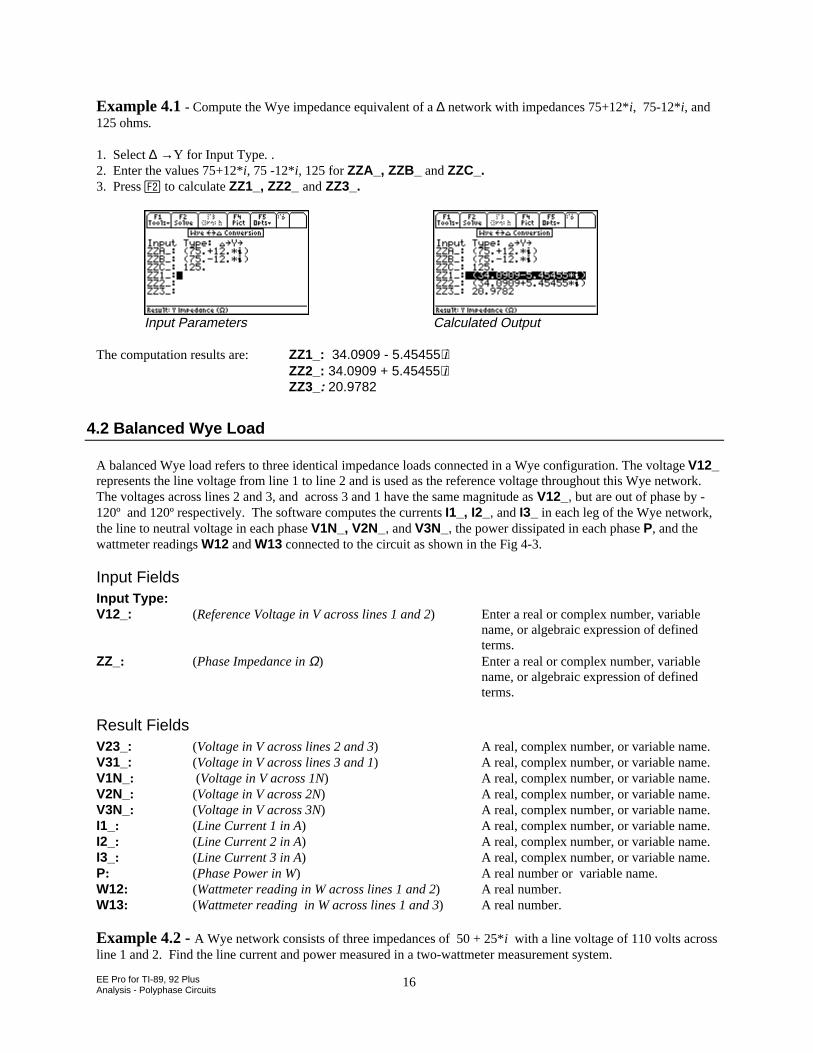
EE Pro for TI-89, 92 PlusAnalysis - Polyphase Circuits
16
Example 4.1 - Compute the Wye impedance equivalent of a ∆ network with impedances 75+12*i, 75-12*i, and125 ohms.
1. Select ∆ →Y for Input Type. .2. Enter the values 75+12*i, 75 -12*i, 125 for ZZA_, ZZB_ and ZZC_.3. Press „ to calculate ZZ1_, ZZ2_ and ZZ3_.
Input Parameters Calculated Output
The computation results are: ZZ1_: 34.0909 - 5.45455⋅iZZ2_: 34.0909 + 5.45455⋅iZZ3_: 20.9782
4.2 Balanced Wye Load
A balanced Wye load refers to three identical impedance loads connected in a Wye configuration. The voltage V12_represents the line voltage from line 1 to line 2 and is used as the reference voltage throughout this Wye network.The voltages across lines 2 and 3, and across 3 and 1 have the same magnitude as V12_, but are out of phase by -120º and 120º respectively. The software computes the currents I1_, I2_, and I3_ in each leg of the Wye network,the line to neutral voltage in each phase V1N_, V2N_, and V3N_, the power dissipated in each phase P, and thewattmeter readings W12 and W13 connected to the circuit as shown in the Fig 4-3.
Input FieldsInput Type:V12_: (Reference Voltage in V across lines 1 and 2) Enter a real or complex number, variable
name, or algebraic expression of defined terms.
ZZ_: (Phase Impedance in Ω) Enter a real or complex number, variablename, or algebraic expression of defined terms.
Result FieldsV23_: (Voltage in V across lines 2 and 3) A real, complex number, or variable name.V31_: (Voltage in V across lines 3 and 1) A real, complex number, or variable name.V1N_: (Voltage in V across 1N) A real, complex number, or variable name.V2N_: (Voltage in V across 2N) A real, complex number, or variable name.V3N_: (Voltage in V across 3N) A real, complex number, or variable name.I1_: (Line Current 1 in A) A real, complex number, or variable name.I2_: (Line Current 2 in A) A real, complex number, or variable name.I3_: (Line Current 3 in A) A real, complex number, or variable name.P: (Phase Power in W) A real number or variable name.W12: (Wattmeter reading in W across lines 1 and 2) A real number.W13: (Wattmeter reading in W across lines 1 and 3) A real number.
Example 4.2 - A Wye network consists of three impedances of 50 + 25*i with a line voltage of 110 volts acrossline 1 and 2. Find the line current and power measured in a two-wattmeter measurement system.
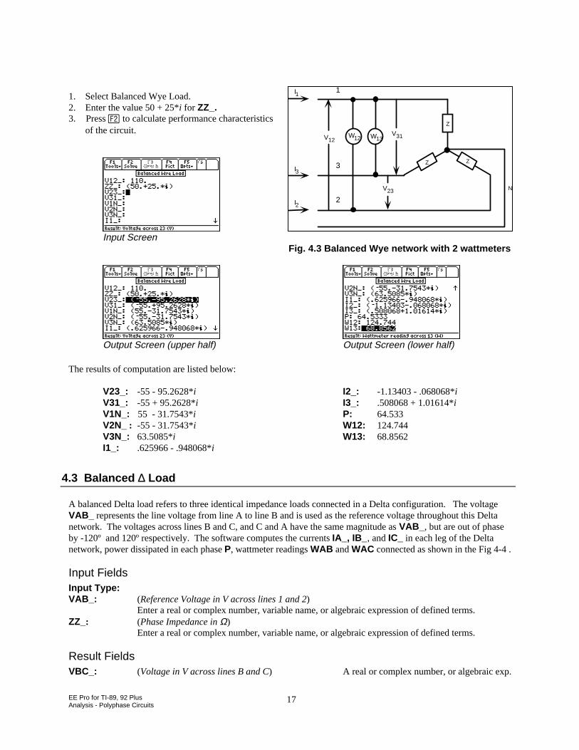
EE Pro for TI-89, 92 PlusAnalysis - Polyphase Circuits
17
1. Select Balanced Wye Load.2. Enter the value 50 + 25*i for ZZ_.3. Press „ to calculate performance characteristics of the circuit.
Input Screen
Fig. 4.3 Balanced Wye network with 2 wattmeters
Output Screen (upper half) Output Screen (lower half)
The results of computation are listed below:
V23_: -55 - 95.2628*iV31_: -55 + 95.2628*iV1N_: 55 - 31.7543*iV2N_ : -55 - 31.7543*iV3N_: 63.5085*iI1_: .625966 - .948068*i
I2_: -1.13403 - .068068*iI3_: .508068 + 1.01614*i P: 64.533W12: 124.744W13: 68.8562
4.3 Balanced ∆ Load
A balanced Delta load refers to three identical impedance loads connected in a Delta configuration. The voltageVAB_ represents the line voltage from line A to line B and is used as the reference voltage throughout this Deltanetwork. The voltages across lines B and C, and C and A have the same magnitude as VAB_ , but are out of phaseby -120º and 120º respectively. The software computes the currents IA_, IB_ , and IC_ in each leg of the Deltanetwork, power dissipated in each phase P, wattmeter readings WAB and WAC connected as shown in the Fig 4-4 .
Input FieldsInput Type:VAB_: (Reference Voltage in V across lines 1 and 2)
Enter a real or complex number, variable name, or algebraic expression of defined terms.ZZ_: (Phase Impedance in Ω)
Enter a real or complex number, variable name, or algebraic expression of defined terms.
Result FieldsVBC_: (Voltage in V across lines B and C) A real or complex number, or algebraic exp.
Z
Z Z
V12W12 W13
V31
V23
I1
I3
I2
N
1
3
2
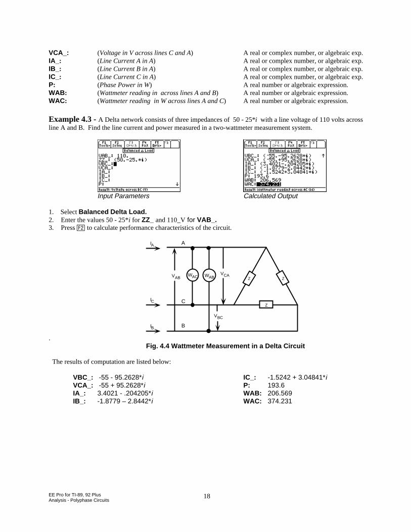
EE Pro for TI-89, 92 PlusAnalysis - Polyphase Circuits
18
VCA_: (Voltage in V across lines C and A) A real or complex number, or algebraic exp.IA_: (Line Current A in A) A real or complex number, or algebraic exp.IB_: (Line Current B in A) A real or complex number, or algebraic exp.IC_: (Line Current C in A) A real or complex number, or algebraic exp.P: (Phase Power in W) A real number or algebraic expression.WAB : (Wattmeter reading in across lines A and B) A real number or algebraic expression.WAC: (Wattmeter reading in W across lines A and C) A real number or algebraic expression.
Example 4.3 - A Delta network consists of three impedances of 50 - 25*i with a line voltage of 110 volts acrossline A and B. Find the line current and power measured in a two-wattmeter measurement system.
Input Parameters Calculated Output
1. Select Balanced Delta Load.2. Enter the values 50 - 25*i for ZZ_ and 110_V for VAB_.3. Press „ to calculate performance characteristics of the circuit.
Z
ZZVAB
WAC WABVCA
VBC
IA
IC
IB
A
C
B
.Fig. 4.4 Wattmeter Measurement in a Delta Circuit
The results of computation are listed below:
VBC_: -55 - 95.2628*iVCA_: -55 + 95.2628*iIA_: 3.4021 - .204205*iIB_: -1.8779 – 2.8442*i
IC_: -1.5242 + 3.04841*iP: 193.6WAB: 206.569WAC: 374.231
EE Pro for TI-89.92 PlusAnalysis - Ladder Networks
19
Chapter 5 Ladder NetworkThis chapter describes ladder network analysis - a circuit reduction method by which branches of the circuit aretreated as sides (series connection) or rungs (parallel or shunt connection) of a ladder.
5.1 Elements of a Ladder Network
In the examples that follow, the left end of the ladder is the input end and the right end of the ladder is the outputend, where the load is connected. The elements of the ladder (from 1 to N) are entered from right to left, goingfrom output to input. The input impedance Zin_ is calculated as if you were “looking in” to the left end of theladder.
Field Descriptions - Input ScreenFrequency: (Frequency) Enter a real number, or algebraic expression of defined terms.Load_: (Initial Load) Enter a real or complex number, variable name, or algebraic expression of defined terms.
1: (Element 1 - closest to the load or output)...N: (Element N - furthest from the load or output)
Field Descriptions - Element ScreenSixteen different element types are available to build the ladder network. These elements can be inserted in seriesor parallel configuration.
ResistorA resistor can be added as a rung (parallel) or side (series). ChooseSeries or Parallel for Config, and enter a value for R in ohms.
Series R Parallel R
R
R
Inductor - (ideal inductor)An inductor can be added as a rung (parallel) or side (series)). ChooseSeries or Parallel for Config, and enter a value for L in henrys.
Series L Parallel L
L
L
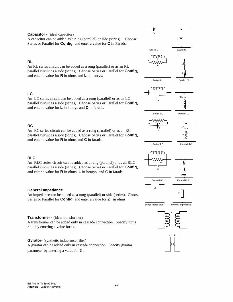
EE Pro for TI-89.92 PlusAnalysis - Ladder Networks
20
Capacitor - (ideal capacitor)A capacitor can be added as a rung (parallel) or side (series). ChooseSeries or Parallel for Config, and enter a value for C in Farads.
Series C Parallel C
C
C
RLAn RL series circuit can be added as a rung (parallel) or as an RLparallel circuit as a side (series). Choose Series or Parallel for Config,and enter a value for R in ohms and L in henrys.
Series RL Parallel RL
R R
L
L
LCAn LC series circuit can be added as a rung (parallel) or as an LCparallel circuit as a side (series). Choose Series or Parallel for Config,and enter a value for L in henrys and C in farads.
Series LC Parallel LC
CC
L
L
RCAn RC series circuit can be added as a rung (parallel) or as an RCparallel circuit as a side (series). Choose Series or Parallel for Config,and enter a value for R in ohms and C in farads.
Series RC Parallel RC
CC
R
R
RLCAn RLC series circuit can be added as a rung (parallel) or as an RLCparallel circuit as a side (series). Choose Series or Parallel for Config,and enter a value for R in ohms, L in henrys, and C in farads.
Series RLC Parallel RLC
L
R
C
R
L
C
General ImpedanceAn impedance can be added as a rung (parallel) or side (series). ChooseSeries or Parallel for Config, and enter a value for Z_ in ohms.
Series Impedance Parallel Impedance
Z
Z
Transformer - (ideal transformer)A transformer can be added only in cascade connection. Specify turnsratio by entering a value for n.
n
Gyrator- (synthetic inductance filter)A gyrator can be added only in cascade connection. Specify gyratorparameter by entering a value for α.
α
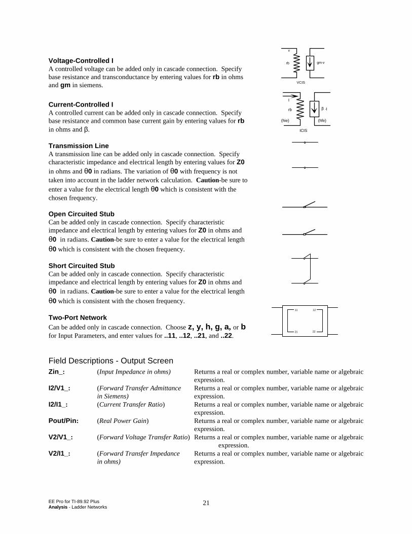
EE Pro for TI-89.92 PlusAnalysis - Ladder Networks
21
Voltage-Controlled IA controlled voltage can be added only in cascade connection. Specifybase resistance and transconductance by entering values for rb in ohmsand gm in siemens.
v
rb
VCIS
gm·v
Current-Controlled IA controlled current can be added only in cascade connection. Specifybase resistance and common base current gain by entering values for rbin ohms and β.
rb
I
β
(hie) (hfe)
ICIS
·I
Transmission LineA transmission line can be added only in cascade connection. Specifycharacteristic impedance and electrical length by entering values for Z0in ohms and θ0 in radians. The variation of θ0 with frequency is nottaken into account in the ladder network calculation. Caution-be sure toenter a value for the electrical length θ0 which is consistent with thechosen frequency.
Open Circuited StubCan be added only in cascade connection. Specify characteristicimpedance and electrical length by entering values for Z0 in ohms andθ0 in radians. Caution-be sure to enter a value for the electrical lengthθ0 which is consistent with the chosen frequency.
Short Circuited StubCan be added only in cascade connection. Specify characteristicimpedance and electrical length by entering values for Z0 in ohms andθ0 in radians. Caution-be sure to enter a value for the electrical lengthθ0 which is consistent with the chosen frequency.
Two-Port NetworkCan be added only in cascade connection. Choose z, y, h, g, a, or bfor Input Parameters, and enter values for ..11, ..12, ..21, and ..22.
11
21
12
22
Field Descriptions - Output ScreenZin_: (Input Impedance in ohms) Returns a real or complex number, variable name or algebraic
expression.I2/V1_: (Forward Transfer Admittance Returns a real or complex number, variable name or algebraic
in Siemens) expression.I2/I1_: (Current Transfer Ratio) Returns a real or complex number, variable name or algebraic
expression.Pout/Pin: (Real Power Gain) Returns a real or complex number, variable name or algebraic
expression.V2/V1_: (Forward Voltage Transfer Ratio) Returns a real or complex number, variable name or algebraic
expression.V2/I1_: (Forward Transfer Impedance Returns a real or complex number, variable name or algebraic
in ohms) expression.
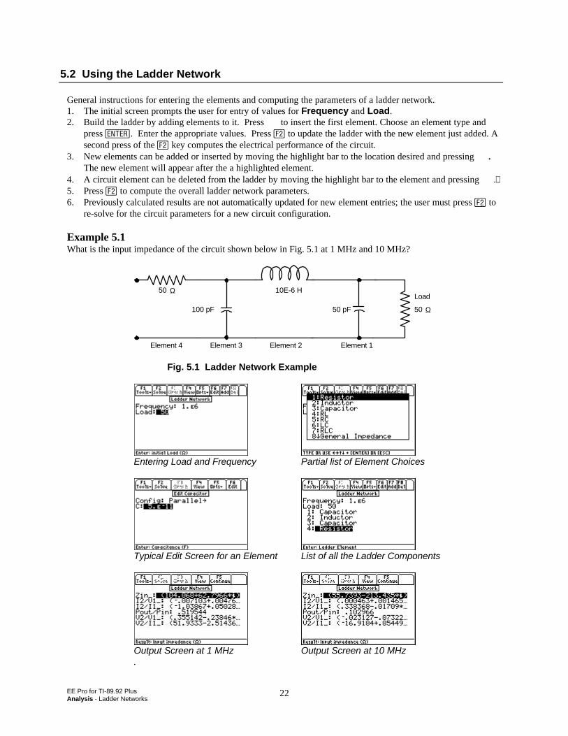
EE Pro for TI-89.92 PlusAnalysis - Ladder Networks
22
5.2 Using the Ladder Network
General instructions for entering the elements and computing the parameters of a ladder network.1. The initial screen prompts the user for entry of values for Frequency and Load.2. Build the ladder by adding elements to it. Press ‰ to insert the first element. Choose an element type and
press ¸. Enter the appropriate values. Press „ to update the ladder with the new element just added. Asecond press of the „ key computes the electrical performance of the circuit.
3. New elements can be added or inserted by moving the highlight bar to the location desired and pressing ‰.The new element will appear after the a highlighted element.
4. A circuit element can be deleted from the ladder by moving the highlight bar to the element and pressing Š...5. Press „ to compute the overall ladder network parameters.6. Previously calculated results are not automatically updated for new element entries; the user must press „ to
re-solve for the circuit parameters for a new circuit configuration.
Example 5.1What is the input impedance of the circuit shown below in Fig. 5.1 at 1 MHz and 10 MHz?
50 Ω
50 Ω 100 pF
10E-6 H
50 pF
Load
Element 1Element 2Element 3Element 4
Fig. 5.1 Ladder Network Example
Entering Load and Frequency Partial list of Element Choices
Typical Edit Screen for an Element List of all the Ladder Components
Output Screen at 1 MHz Output Screen at 10 MHz.
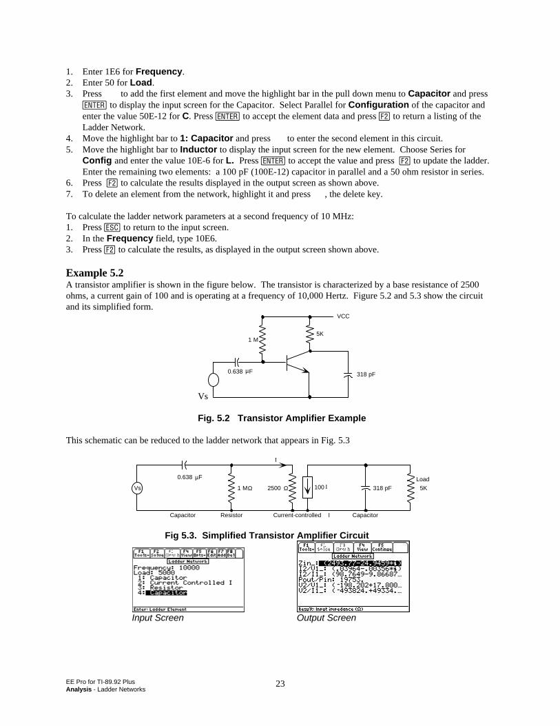
EE Pro for TI-89.92 PlusAnalysis - Ladder Networks
23
1. Enter 1E6 for Frequency.2. Enter 50 for Load.3. Press ‰ to add the first element and move the highlight bar in the pull down menu to Capacitor and press
¸ to display the input screen for the Capacitor. Select Parallel for Configuration of the capacitor andenter the value 50E-12 for C. Press ¸ to accept the element data and press „ to return a listing of theLadder Network.
4. Move the highlight bar to 1: Capacitor and press ‰ to enter the second element in this circuit.5. Move the highlight bar to Inductor to display the input screen for the new element. Choose Series for
Config and enter the value 10E-6 for L. Press ¸ to accept the value and press „ to update the ladder.Enter the remaining two elements: a 100 pF (100E-12) capacitor in parallel and a 50 ohm resistor in series.
6. Press „ to calculate the results displayed in the output screen as shown above.7. To delete an element from the network, highlight it and press Š, the delete key.
To calculate the ladder network parameters at a second frequency of 10 MHz:1. Press N to return to the input screen.2. In the Frequency field, type 10E6.3. Press „ to calculate the results, as displayed in the output screen shown above.
Example 5.2A transistor amplifier is shown in the figure below. The transistor is characterized by a base resistance of 2500ohms, a current gain of 100 and is operating at a frequency of 10,000 Hertz. Figure 5.2 and 5.3 show the circuitand its simplified form.
Vs
1 M5K
318 pF0.638 µF
VCC
Fig. 5.2 Transistor Amplifier Example
This schematic can be reduced to the ladder network that appears in Fig. 5.3
I
100 I 318 pF 5K1 M Ω 2500 Ω
0.638 µF
Vs
Current-controlled IResistor CapacitorCapacitor
Load
Fig 5.3. Simplified Transistor Amplifier Circuit
Input Screen Output Screen

EE Pro for TI-89.92 PlusAnalysis - Ladder Networks
24
1. Enter the frequency and load values: Frequency: 10,000 Hz. Load: 5000 ohms.2. Enter the ladder elements in the following order:
Capacitor: Parallel, 318E-12. Current-Controlled I: Enter 2500 ohms for RB and 100 for β. Resistor: Parallel, 1E6 ohms. Capacitor: Series, 0.638E-6 farads.
3. Press „ to compute the results, which are displayed in the output screen above.
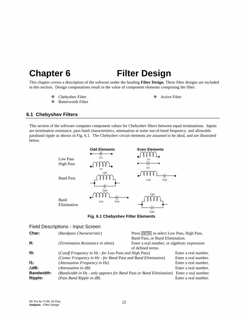
EE Pro for TI-89, 92 PlusAnalysis - Filter Design
25
Chapter 6 Filter DesignThis chapter covers a description of the software under the heading Filter Design. Three filter designs are includedin this section. Design computations result in the value of component elements comprising the filter.
v Chebyshev Filterv Butterworth Filter
v Active Filter
6.1 Chebyshev Filters
This section of the software computes component values for Chebyshev filters between equal terminations. Inputsare termination resistance, pass band characteristics, attenuation at some out-of-band frequency, and allowablepassband ripple as shown in Fig. 6.1. The Chebyshev circuit elements are assumed to be ideal, and are illustratedbelow.
Odd Elements Even Elements
Low Pass CnLn
High PassLn Cn
Band PassLpn
Cpn
Lsn Csn
BandElimination
Lsn Csn
Lpn
Cpn
Fig. 6.1 Chebyshev Filter Elements
Field Descriptions - Input ScreenChar: (Bandpass Characteristic) Press ¸ to select Low Pass, High Pass,
Band Pass, or Band Elimination.R: (Termination Resistance in ohms) Enter a real number, or algebraic expression
of defined terms.f0: (Cutoff Frequency in Hz - for Low Pass and High Pass) Enter a real number. (Center Frequency in Hz - for Band Pass and Band Elimination) Enter a real number.f1: (Attenuation Frequency in Hz) Enter a real number.∆dB: (Attenuation in dB) Enter a real number.Bandwidth: (Bandwidth in Hz - only appears for Band Pass or Band Elimination) Enter a real number.Ripple: (Pass Band Ripple in dB) Enter a real number.
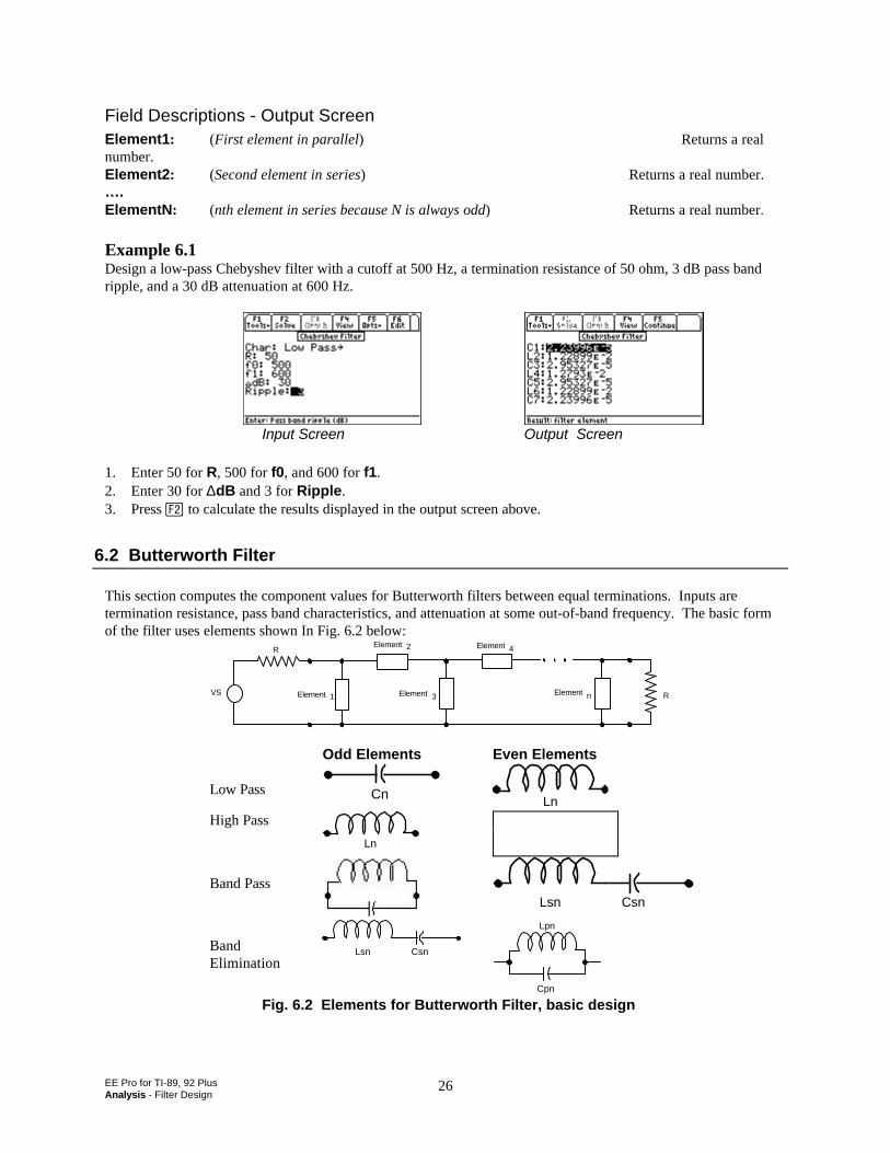
EE Pro for TI-89, 92 PlusAnalysis - Filter Design
26
Field Descriptions - Output ScreenElement1: (First element in parallel) Returns a realnumber.Element2: (Second element in series) Returns a real number.….ElementN: (nth element in series because N is always odd) Returns a real number.
Example 6.1Design a low-pass Chebyshev filter with a cutoff at 500 Hz, a termination resistance of 50 ohm, 3 dB pass bandripple, and a 30 dB attenuation at 600 Hz.
Input Screen Output Screen
1. Enter 50 for R, 500 for f0, and 600 for f1.2. Enter 30 for ∆dB and 3 for Ripple.3. Press „ to calculate the results displayed in the output screen above.
6.2 Butterworth Filter
This section computes the component values for Butterworth filters between equal terminations. Inputs aretermination resistance, pass band characteristics, and attenuation at some out-of-band frequency. The basic formof the filter uses elements shown In Fig. 6.2 below:
Element n
R Element 4
Element 1 Element 3 RVS
Element 2
Odd Elements Even Elements
Low Pass Cn LnHigh Pass
Ln
Band PassLsn Csn
BandElimination
Lsn Csn
Lpn
Cpn
Fig. 6.2 Elements for Butterworth Filter, basic design
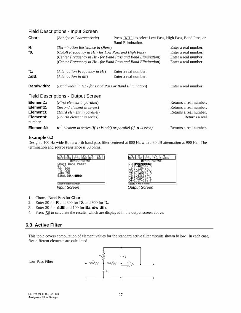
EE Pro for TI-89, 92 PlusAnalysis - Filter Design
27
Field Descriptions - Input ScreenChar: (Bandpass Characteristic) Press ¸ to select Low Pass, High Pass, Band Pass, or
Band Elimination.R: (Termination Resistance in Ohms) Enter a real number.f0: (Cutoff Frequency in Hz - for Low Pass and High Pass) Enter a real number.
(Center Frequency in Hz - for Band Pass and Band Elimination) Enter a real number.(Center Frequency in Hz - for Band Pass and Band Elimination) Enter a real number.
f1: (Attenuation Frequency in Hz) Enter a real number.∆dB: (Attenuation in dB) Enter a real number.
Bandwidth: (Band width in Hz - for Band Pass or Band Elimination) Enter a real number.
Field Descriptions - Output ScreenElement1: (First element in parallel) Returns a real number.Element2: (Second element in series) Returns a real number.Element3: (Third element in parallel) Returns a real number.Element4: (Fourth element in series) Returns a realnumber.ElementN: nth element in series (if n is odd) or parallel (if n is even) Returns a real number.
Example 6.2Design a 100 Hz wide Butterworth band pass filter centered at 800 Hz with a 30 dB attenuation at 900 Hz. Thetermination and source resistance is 50 ohms.
Input Screen Output Screen
1. Choose Band Pass for Char.2. Enter 50 for R and 800 for f0, and 900 for f1.3. Enter 30 for ∆dB and 100 for Bandwidth.4. Press „ to calculate the results, which are displayed in the output screen above.
6.3 Active Filter
This topic covers computation of element values for the standard active filter circuits shown below. In each case,five different elements are calculated.
Low Pass Filter -
+
C5
R3
R4
R1
C2
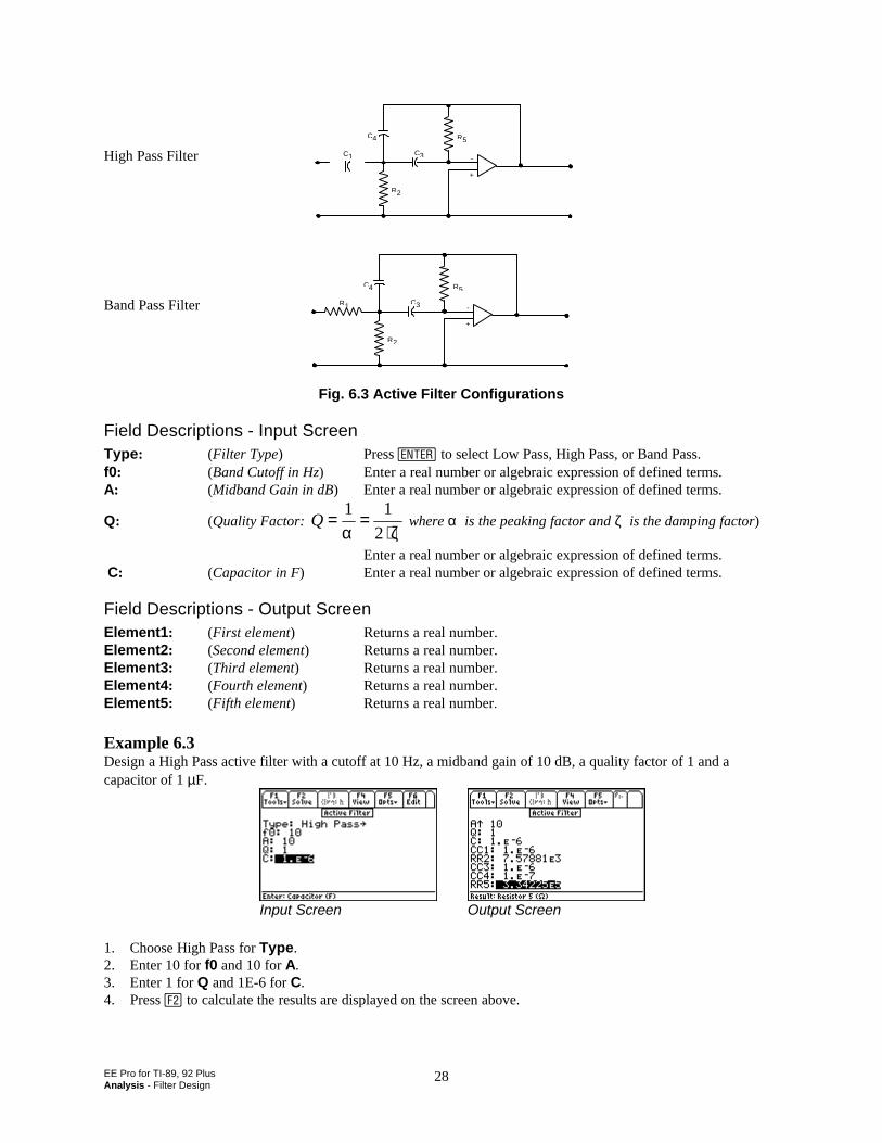
EE Pro for TI-89, 92 PlusAnalysis - Filter Design
28
High Pass Filter
-
+
R5
C3
C4
C1
R2
Band Pass Filter -
+
R5
C3
C4
R1
R2
Fig. 6.3 Active Filter Configurations
Field Descriptions - Input ScreenType: (Filter Type) Press ¸ to select Low Pass, High Pass, or Band Pass.f0: (Band Cutoff in Hz) Enter a real number or algebraic expression of defined terms.A: (Midband Gain in dB) Enter a real number or algebraic expression of defined terms.
Q: (Quality Factor: Q = =⋅
1 12α ζ
where α is the peaking factor and ζ is the damping factor)
Enter a real number or algebraic expression of defined terms. C: (Capacitor in F) Enter a real number or algebraic expression of defined terms.
Field Descriptions - Output ScreenElement1: (First element) Returns a real number.Element2: (Second element) Returns a real number.Element3: (Third element) Returns a real number.Element4: (Fourth element) Returns a real number.Element5: (Fifth element) Returns a real number.
Example 6.3Design a High Pass active filter with a cutoff at 10 Hz, a midband gain of 10 dB, a quality factor of 1 and acapacitor of 1 µF.
Input Screen Output Screen
1. Choose High Pass for Type.2. Enter 10 for f0 and 10 for A.3. Enter 1 for Q and 1E-6 for C.4. Press „ to calculate the results are displayed on the screen above.
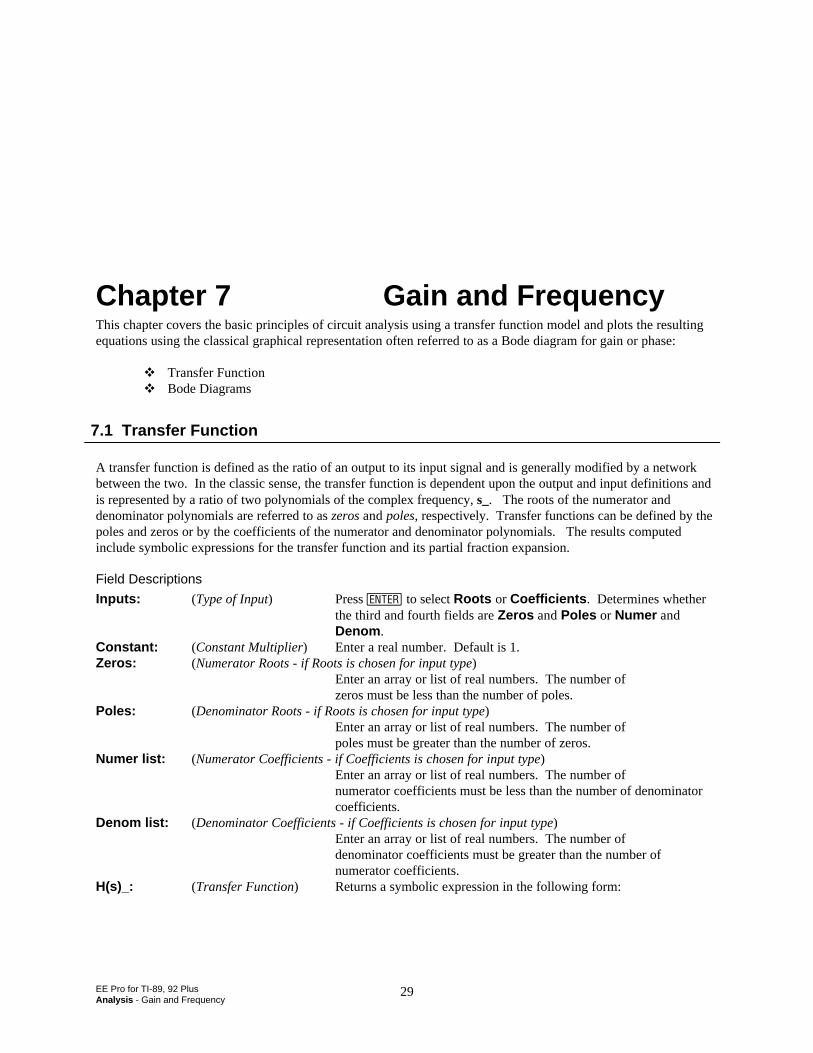
EE Pro for TI-89, 92 PlusAnalysis - Gain and Frequency
29
Chapter 7 Gain and FrequencyThis chapter covers the basic principles of circuit analysis using a transfer function model and plots the resultingequations using the classical graphical representation often referred to as a Bode diagram for gain or phase:
v Transfer Functionv Bode Diagrams
7.1 Transfer Function
A transfer function is defined as the ratio of an output to its input signal and is generally modified by a networkbetween the two. In the classic sense, the transfer function is dependent upon the output and input definitions andis represented by a ratio of two polynomials of the complex frequency, s_. The roots of the numerator anddenominator polynomials are referred to as zeros and poles, respectively. Transfer functions can be defined by thepoles and zeros or by the coefficients of the numerator and denominator polynomials. The results computedinclude symbolic expressions for the transfer function and its partial fraction expansion.
Field Descriptions
Inputs: (Type of Input) Press ¸ to select Roots or Coefficients. Determines whetherthe third and fourth fields are Zeros and Poles or Numer andDenom.
Constant: (Constant Multiplier) Enter a real number. Default is 1.Zeros: (Numerator Roots - if Roots is chosen for input type)
Enter an array or list of real numbers. The number ofzeros must be less than the number of poles.
Poles: (Denominator Roots - if Roots is chosen for input type)Enter an array or list of real numbers. The number ofpoles must be greater than the number of zeros.
Numer list: (Numerator Coefficients - if Coefficients is chosen for input type)Enter an array or list of real numbers. The number ofnumerator coefficients must be less than the number of denominatorcoefficients.
Denom list: (Denominator Coefficients - if Coefficients is chosen for input type)Enter an array or list of real numbers. The number ofdenominator coefficients must be greater than the number ofnumerator coefficients.
H(s)_: (Transfer Function) Returns a symbolic expression in the following form:
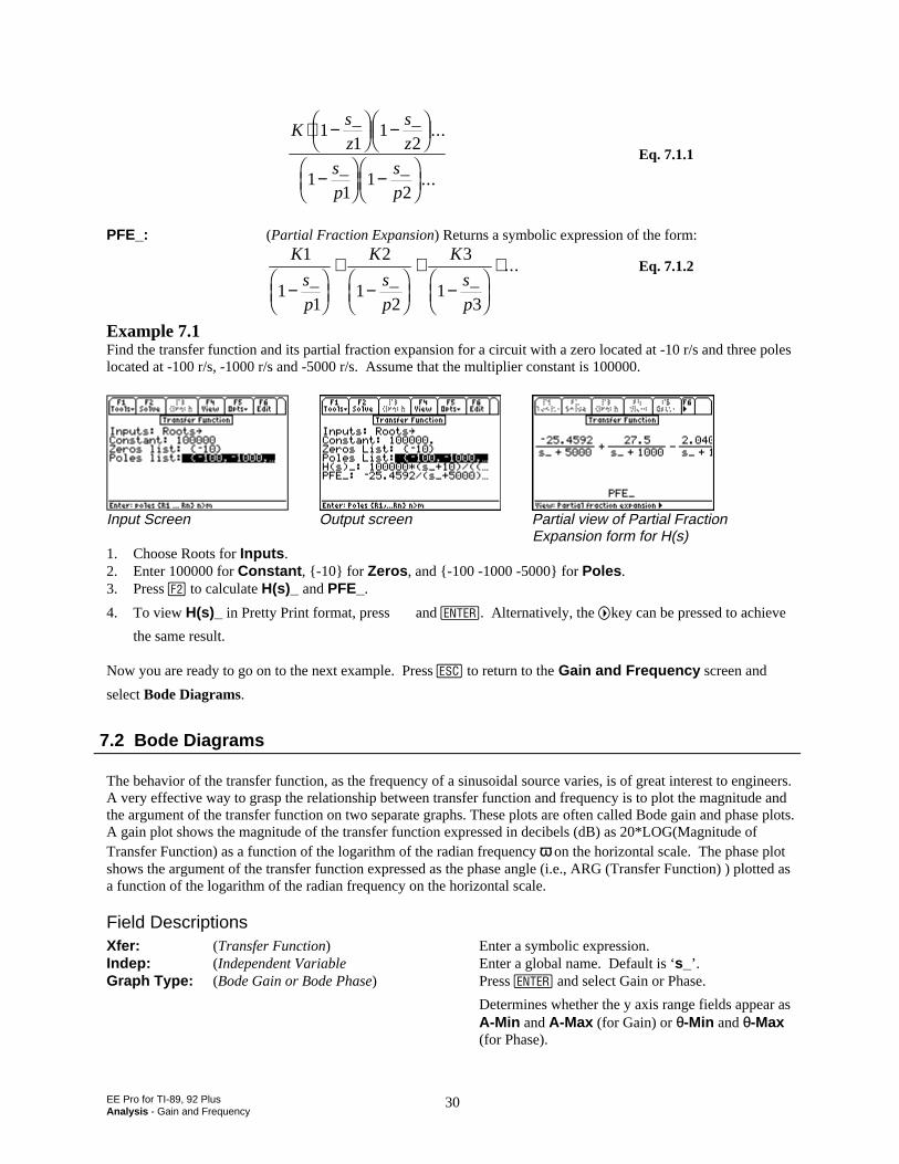
EE Pro for TI-89, 92 PlusAnalysis - Gain and Frequency
30
Ks
z
s
z
s
p
s
p
⋅ −FHG
IKJ −FHG
IKJ
−FHG
IKJ −FHG
IKJ
11
12
11
12
_ _...
_ _...
Eq. 7.1.1
PFE_: (Partial Fraction Expansion) Returns a symbolic expression of the form:K
s
p
K
s
p
K
s
p
1
11
2
12
3
13
−FHG
IKJ
+−F
HGIKJ
+−F
HGIKJ
+_ _ _
... Eq. 7.1.2
Example 7.1Find the transfer function and its partial fraction expansion for a circuit with a zero located at -10 r/s and three poleslocated at -100 r/s, -1000 r/s and -5000 r/s. Assume that the multiplier constant is 100000.
Input Screen Output screen Partial view of Partial FractionExpansion form for H(s)
1. Choose Roots for Inputs .2. Enter 100000 for Constant , -10 for Zeros , and -100 -1000 -5000 for Poles .3. Press „ to calculate H(s)_ and PFE_.
4. To view H(s)_ in Pretty Print format, press ‡ and . Alternatively, the Bkey can be pressed to achieve
the same result.
Now you are ready to go on to the next example. Press N to return to the Gain and Frequency screen and
select Bode Diagrams.
7.2 Bode Diagrams
The behavior of the transfer function, as the frequency of a sinusoidal source varies, is of great interest to engineers.A very effective way to grasp the relationship between transfer function and frequency is to plot the magnitude andthe argument of the transfer function on two separate graphs. These plots are often called Bode gain and phase plots.A gain plot shows the magnitude of the transfer function expressed in decibels (dB) as 20*LOG(Magnitude ofTransfer Function) as a function of the logarithm of the radian frequency ω on the horizontal scale. The phase plotshows the argument of the transfer function expressed as the phase angle (i.e., ARG (Transfer Function) ) plotted asa function of the logarithm of the radian frequency on the horizontal scale.
Field DescriptionsXfer: (Transfer Function) Enter a symbolic expression.Indep: (Independent Variable Enter a global name. Default is ‘s_’.Graph Type: (Bode Gain or Bode Phase) Press and select Gain or Phase.
Determines whether the y axis range fields appear asA-Min and A-Max (for Gain) or θ-Min and θ-Max (for Phase).
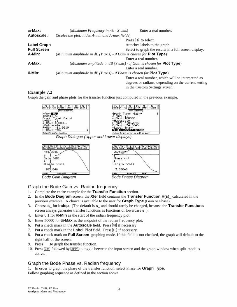
EE Pro for TI-89, 92 PlusAnalysis - Gain and Frequency
31
ω-Max: (Maximum Frequency in r/s - X axis) Enter a real number.Autoscale: (Scales the plot: hides A-min and A-max fields)
Press ˆ to select.Label Graph Attaches labels to the graph.Full Screen Select to graph the results in a full screen display. A-Min: (Minimum amplitude in dB (Y axis) - if Gain is chosen for Plot Type)
Enter a real number.A-Max: (Maximum amplitude in dB (Y axis) - if Gain is chosen for Plot Type)
Enter a real number.θ-Min: (Minimum amplitude in dB (Y axis) - if Phase is chosen for Plot Type)
Enter a real number, which will be interpreted as degrees or radians, depending on the current setting in the Custom Settings screen.
Example 7.2Graph the gain and phase plots for the transfer function just computed in the previous example.
Graph Dialogue (Upper and Lower displays)
Bode Gain Diagram Bode Phase Diagram
Graph the Bode Gain vs. Radian frequency1. Complete the entire example for the Transfer Function section.2. In the Bode Diagram screen, the Xfer field contains the Transfer Function H(s)_ calculated in the
previous example. A choice is available to the user for Graph Type (Gain or Phase).3. Choose s_ for Indep. (The default is s_ and should rarely be changed, because the Transfer Functions
screen always generates transfer functions as functions of lowercase s_).4. Enter 0.1 for ω-Min as the start of the radian frequency plot.5. Enter 50000 for ω-Max as the endpoint of the radian frequency plot.6. Put a check mark in the Autoscale field. Press ˆ if necessary7. Put a check mark in the Label Plot field. Press ˆ if necessary.8. Put a check mark on Full Screen graphing mode. If this field is not checked, the graph will default to the
right half of the screen.9. Press … to graph the transfer function.10. Press 2 followed by Oto toggle between the input screen and the graph window when split-mode is
active.
Graph the Bode Phase vs. Radian frequency1. In order to graph the phase of the transfer function, select Phase for Graph Type.Follow graphing sequence as defined in the section above.

EE Pro for TI-89, 92 PlusAnalysis - FFT
32
Chapter 8 Fourier TransformsThis section contains software computing discrete “Fast” Fourier transforms and its inverse.
v FFT v Inverse FFT
8.1 FFT
A physical process can be monitored in two significantly different ways. First, the process can be monitored intime domain in analog or digital form. Second, the data can be collected in the frequency domain in analog ordigital form. In a variety of measurement and digital storage devices, data is gathered at regular, discrete timeintervals. This data can be converted to its equivalent set in the frequency domain by the use of the so-called FFTalgorithm. This algorithm maps a data array of N items to the corresponding array in the frequency domain usingthe following equation.
H h ek nn 0
N 1-2 j k n N= ⋅
=
−⋅ ⋅∑ π
Eq. 8.1.1
The variable hn is the nth element in the time domain and Hk is the kth element in the frequency domain. TheFFT algorithm treats the data block provided as though it is one of a periodic sequence. If the underlying data isnot periodic, the resulting FFT-created wave is subject to substantial harmonic distortion. This section does notpad the input array with 0’s when the number of data points is not a power of 2.
Field DescriptionsTime: (Time Signal) Enter an array or list of real or complex numbers.Freq: (Frequency Spectrum) Returns spectral coefficients.
Example 8.1Find spectral coefficients for the periodic time signal [1 2 3 4].1. Enter [1 2 3 4] for Time.2. Press „ to calculate and display results in the frequency domain Freq.3. The screen display of the output and the input are shown below.
←Input Screen
Output of Computation→
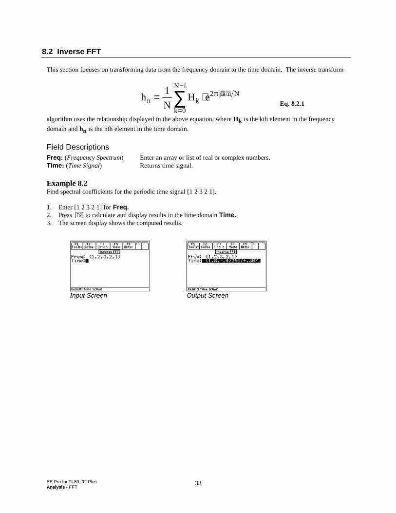
EE Pro for TI-89, 92 PlusAnalysis - FFT
33
8.2 Inverse FFT
This section focuses on transforming data from the frequency domain to the time domain. The inverse transform
h1N
H en k2 j k n N
k 0
N 1
= ⋅ ⋅ ⋅
=
−
∑ πEq. 8.2.1
algorithm uses the relationship displayed in the above equation, where Hk is the kth element in the frequencydomain and hn is the nth element in the time domain.
Field DescriptionsFreq: (Frequency Spectrum) Enter an array or list of real or complex numbers.Time: (Time Signal) Returns time signal.
Example 8.2 Find spectral coefficients for the periodic time signal [1 2 3 2 1].
1. Enter [1 2 3 2 1] for Freq.2. Press „ to calculate and display results in the time domain Time.3. The screen display shows the computed results.
Input Screen Output Screen
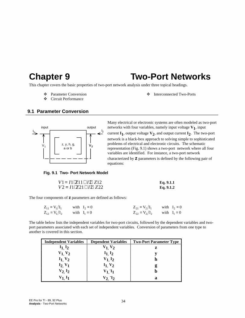
EE Pro for TI - 89, 92 PlusAnalysis - Two-Port Networks
34
Chapter 9 Two-Port NetworksThis chapter covers the basic properties of two-port network analysis under three topical headings.
Parameter ConversionCircuit Performance
Interconnected Two-Ports
9.1 Parameter Conversion
Many electrical or electronic systems are often modeled as two-portnetworks with four variables, namely input voltage V1, input
current I1, output voltage V2, and output current I2. The two-port
network is a black-box approach to solving simple to sophisticatedproblems of electrical and electronic circuits. The schematicrepresentation (Fig. 9.1) shows a two-port network where all fourvariables are identified. For instance, a two-port networkcharacterized by z parameters is defined by the following pair ofequations:
Fig. 9.1 Two- Port Network Model
V I Z I Z1 1 11 2 12= ⋅ + ⋅ Eq. 9.1.1 V I Z I Z2 1 21 2 22= ⋅ + ⋅ Eq. 9.1.2
The four components of z parameters are defined as follows:
Z V I11 1 1= with I 02 =Z V I12 1 2= with I 01 =
Z V I21 2 1= with I 02 =Z V I22 2 2= with I 01 =
The table below lists the independent variables for two-port circuits, followed by the dependent variables and two-port parameters associated with each set of independent variables. Conversion of parameters from one type toanother is covered in this section.
Independent Variables Dependent Variables Two-Port Parameter TypeI1, I2 V1, V2 z
V1, V2 I1, I2 yI1, V2 V1, I2 hI2, V1 I1, V2 gV2, I2 V1,
-I1 bV1, I1 V2,
-I2 a
z, y, h, g,a or b
V2V1
I2I1input output
V2
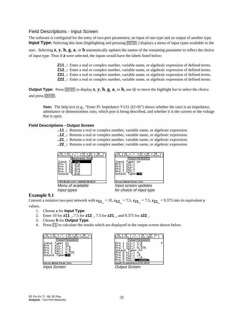
EE Pro for TI - 89, 92 PlusAnalysis - Two-Port Networks
35
Field Descriptions - Input ScreenThe software is configured for the entry of two-port parameters; an input of one type and an output of another type.Input Type : Selecting this item (highlighting and pressing ¸ ) displays a menu of input types available to the
user. Selecting z, y, h, g, a, or b automatically updates the names of the remaining parameter to reflect the choice
of input type. Thus if z were selected, the inputs would have the labels listed below:
Z11_: Enter a real or complex number, variable name, or algebraic expression of defined terms.Z12_: Enter a real or complex number, variable name, or algebraic expression of defined terms.Z21_: Enter a real or complex number, variable name, or algebraic expression of defined terms.Z22_: Enter a real or complex number, variable name, or algebraic expression of defined terms.
Output Type : Press to display z, y, h, g, a, or b, use D to move the highlight bar to select the choice
and press .
Note: The help text (e.g., “Enter P1 Impedance V1/I1 (I2=0)”) shows whether the ratio is an impedance,admittance or dimensionless ratio, which port is being described, and whether it is the current or the voltagethat is open.
Field Descriptions - Output Screen..11_: Returns a real or complex number, variable name, or algebraic expression...12_: Returns a real or complex number, variable name, or algebraic expression...21_: Returns a real or complex number, variable name, or algebraic expression...22_: Returns a real or complex number, variable name, or algebraic expression.
Menu of available Input screen updatesInput types for choice of input type
Example 9.1Convert a resistive two-port network with z11_ = 10, z12_ = 7.5, z21_ = 7.5, z22_ = 9.375 into its equivalent y
values.1. Choose z for Input Type .2. Enter 10 for z11_, 7.5 for z12_, 7.5 for z21_, and 9.375 for z22_.3. Choose h for Output Type .4. Press „ to calculate the results which are displayed in the output screen shown below.
Input Screen Output Screen
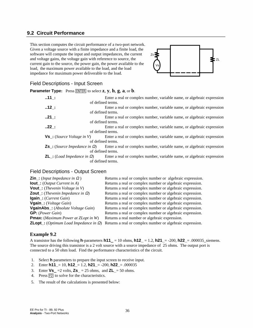
EE Pro for TI - 89, 92 PlusAnalysis - Two-Port Networks
36
9.2 Circuit Performance
This section computes the circuit performance of a two-port network.Given a voltage source with a finite impedance and a finite load, thesoftware will compute the input and output impedances, the currentand voltage gains, the voltage gain with reference to source, thecurrent gain to the source, the power gain, the power available to theload, the maximum power available to the load, and the loadimpedance for maximum power deliverable to the load.
Field Descriptions - Input ScreenParameter Type : Press to select z, y, h, g, a, or b.
..11_: Enter a real or complex number, variable name, or algebraic expression of defined terms.
..12_: Enter a real or complex number, variable name, or algebraic expression of defined terms.
..21_: Enter a real or complex number, variable name, or algebraic expression of defined terms.
..22_: Enter a real or complex number, variable name, or algebraic expression of defined terms.
Vs_: (Source Voltage in V) Enter a real or complex number, variable name, or algebraic expression of defined terms.
Zs_: (Source Impedance in Ω) Enter a real or complex number, variable name, or algebraic expression of defined terms.
ZL_: (Load Impedance in Ω) Enter a real or complex number, variable name, or algebraic expression of defined terms.
Field Descriptions - Output ScreenZin_: (Input Impedance in Ω ) Returns a real or complex number or algebraic expression.Iout_: (Output Current in A) Returns a real or complex number or algebraic expression.Vout_: (Thevenin Voltage in V) Returns a real or complex number or algebraic expression.Zout_: (Thevenin Impedance in Ω) Returns a real or complex number or algebraic expression.Igain_ : (Current Gain) Returns a real or complex number or algebraic expression.Vgain_ : (Voltage Gain) Returns a real or complex number or algebraic expression.VgainAbs_: (Absolute Voltage Gain) Returns a real or complex number or algebraic expression.GP: (Power Gain) Returns a real or complex number or algebraic expression.Pmax : (Maximum Power at ZLopt in W) Returns a real number or algebraic expression.ZLopt_ : (Optimum Load Impedance in Ω) Returns a real or complex number or algebraic expression.
Example 9.2 A transistor has the following h-parameters h11_ = 10 ohms, h12_ = 1.2, h21_= -200, h22_= .000035_siemens.The source driving this transistor is a 2 volt source with a source impedance of 25 ohms. The output port isconnected to a 50 ohm load. Find the performance characteristics of the circuit.
1. Select h parameters to prepare the input screen to receive input.2. Enter h11_= 10, h12_= 1.2, h21_= -200, h22_= .0000353. Enter Vs_ =2 volts, Zs_ = 25 ohms, and ZL_= 50 ohms.4. Press „ to solve for the characteristics.
5. The result of the calculations is presented below:
Vs
Zs
ZL
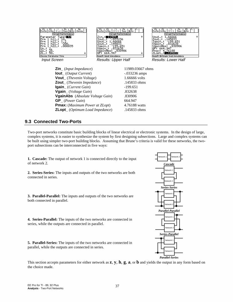
EE Pro for TI - 89, 92 PlusAnalysis - Two-Port Networks
37
Input Screen Results: Upper Half Results: Lower Half
Zin_ (Input Impedance) 11989.03667 ohmsIout_ (Output Current) -.033236 ampsVout_ (Thevenin Voltage) 1.66666 voltsZout_ (Thevenin Impedance) .145833 ohmsIgain_ (Current Gain) -199.651Vgain_ (Voltage Gain) .832638VgainAbs (Absolute Voltage Gain) .830906GP_ (Power Gain) 664.947Pmax : (Maximum Power at ZLopt) 4.76188 wattsZLopt_ (Optimum Load Impedance) .145833 ohms
9.3 Connected Two-Ports
Two-port networks constitute basic building blocks of linear electrical or electronic systems. In the design of large,complex systems, it is easier to synthesize the system by first designing subsections. Large and complex systems canbe built using simpler two-port building blocks. Assuming that Brune’s criteria is valid for these networks, the two-port subsections can be interconnected in five ways:
1. Cascade: The output of network 1 is connected directly to the inputof network 2.
Network 1 Network 2
Cascade
2. Series-Series: The inputs and outputs of the two networks are bothconnected in series.
Network 1
Network 2
Series-Series
3. Parallel-Parallel: The inputs and outputs of the two networks areboth connected in parallel.
Network 1
Network 2
Parallel-Parallel
4. Series-Parallel: The inputs of the two networks are connected inseries, while the outputs are connected in parallel.
Network 1
Network 2
Series-Parallel
5. Parallel-Series: The inputs of the two networks are connected inparallel, while the outputs are connected in series.
Network 1
Network 2
Parallel-Series
This section accepts parameters for either network as z, y, h, g, a, or b and yields the output in any form based onthe choice made.

EE Pro for TI - 89, 92 PlusAnalysis - Two-Port Networks
38
Field Descriptions - Input ScreenConnection : (Type of Connection) Press to select Cascade, Series Series, Parallel Parallel, Series
Parallel, or Parallel Series.First Input Type : Press to select parameter type z, y, h, g, a, or b for entry.
..111_: Enter a real or complex number, variable name, or algebraic expression of defined terms.
..112_: Enter a real or complex number, variable name, or algebraic expression of defined terms.
..121_: Enter a real or complex number, variable name, or algebraic expression of defined terms.
..122_: Enter a real or complex number, variable name, or algebraic expression of defined terms.
Second Input Type : Press to select parameter type z, y, h, g, a, or b for entry.
..211_: Enter a real or complex number, variable name, or algebraic expression of defined terms.
..212_: Enter a real or complex number, variable name, or algebraic expression of defined terms.
..221_: Enter a real or complex number, variable name, or algebraic expression of defined terms.
..222_: Enter a real or complex number, variable name, or algebraic expression of defined terms.
Output Type : Press to select z, y, h, g, a, or b...11_: Returns a real or complex number, variable name, or algebraic expression of defined terms...12_: Returns a real or complex number, variable name, or algebraic expression of defined terms...21_: Returns a real or complex number, variable name, or algebraic expression of defined terms...22_: Returns a real or complex number, variable name, or algebraic expression of defined terms.
Example 9.3The 2 two-port networks are defined in terms of their z and h parameters. The z parameters are 10, 7.5, 7.5, 9.375
respectively while the h parameters are 25, .001, 100, .0025. If the two-ports are connected in a cascade
configuration, compute the y parameters for the resulting equivalent two-port. To solve this problem:
1. Choose Cascade for Connection .2. Choose z for First Input Type .
3. Enter 10 for z11_, 7.5 for z12_, 7.5 for z21_, and 9.375 for z22_.4. Choose h for Second Input Type .
5. Enter 25 for h11_, .001 for h12_, 100 for h21_, and .0025 for h22_.
6. Choose y for Output Type .7. Press „ to complete the computation. The resulting data is shown in the screen displays shown.
Input screen showing Input screen showing h Output screen showing yz parameters for the parameters for the parameters of the combinedfirst two-port. Second two-port. Two-port.
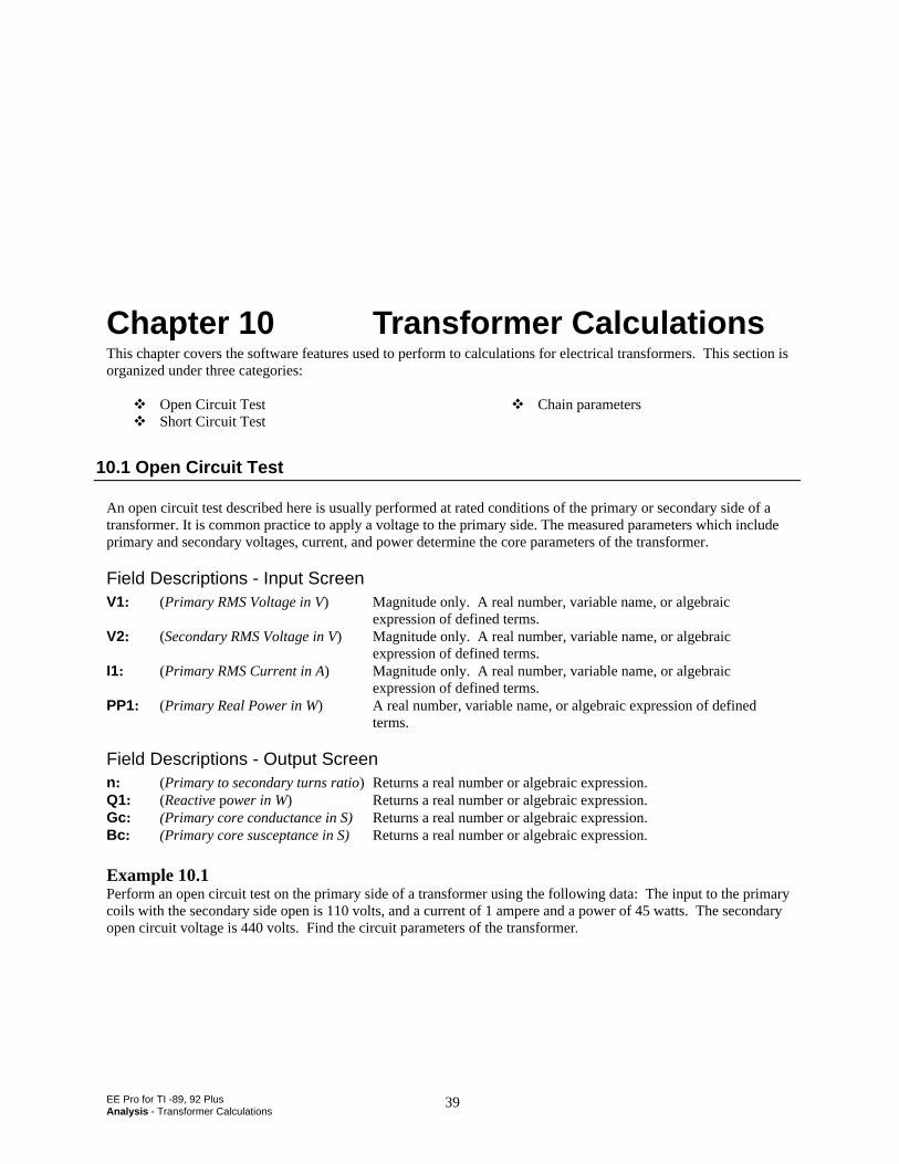
EE Pro for TI -89, 92 PlusAnalysis - Transformer Calculations
39
Chapter 10 Transformer CalculationsThis chapter covers the software features used to perform to calculations for electrical transformers. This section isorganized under three categories:
Open Circuit TestShort Circuit Test
Chain parameters
10.1 Open Circuit Test
An open circuit test described here is usually performed at rated conditions of the primary or secondary side of atransformer. It is common practice to apply a voltage to the primary side. The measured parameters which includeprimary and secondary voltages, current, and power determine the core parameters of the transformer.
Field Descriptions - Input ScreenV1: (Primary RMS Voltage in V) Magnitude only. A real number, variable name, or algebraic
expression of defined terms.V2: (Secondary RMS Voltage in V) Magnitude only. A real number, variable name, or algebraic
expression of defined terms.I1: (Primary RMS Current in A) Magnitude only. A real number, variable name, or algebraic
expression of defined terms.PP1: (Primary Real Power in W) A real number, variable name, or algebraic expression of defined
terms.
Field Descriptions - Output Screenn: (Primary to secondary turns ratio) Returns a real number or algebraic expression.Q1: (Reactive power in W) Returns a real number or algebraic expression.Gc: (Primary core conductance in S) Returns a real number or algebraic expression.Bc : (Primary core susceptance in S) Returns a real number or algebraic expression.
Example 10.1Perform an open circuit test on the primary side of a transformer using the following data: The input to the primarycoils with the secondary side open is 110 volts, and a current of 1 ampere and a power of 45 watts. The secondaryopen circuit voltage is 440 volts. Find the circuit parameters of the transformer.
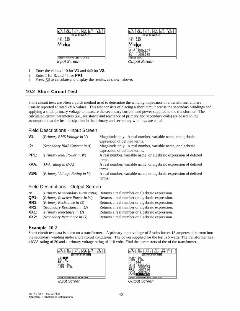
EE Pro for TI -89, 92 PlusAnalysis - Transformer Calculations
40
Input Screen Output Screen
1. Enter the values 110 for V1 and 440 for V2.2. Enter 1 for I1 and 45 for PP1.3. Press „ to calculate and display the results, as shown above.
10.2 Short Circuit Test
Short circuit tests are often a quick method used to determine the winding impedance of a transformer and areusually reported at rated kVA values. This test consists of placing a short circuit across the secondary windings andapplying a small primary voltage to measure the secondary current, and power supplied to the transformer. Thecalculated circuit parameters (i.e., resistance and reactance of primary and secondary coils) are based on theassumption that the heat dissipation in the primary and secondary windings are equal.
Field Descriptions - Input ScreenV1: (Primary RMS Voltage in V) Magnitude only. A real number, variable name, or algebraic
expression of defined terms.I2: (Secondary RMS Current in A) Magnitude only. A real number, variable name, or algebraic
expression of defined terms.PP1: (Primary Real Power in W) A real number, variable name, or algebraic expression of defined
terms.kVA : (kVA rating in kVA) A real number, variable name, or algebraic expression of defined
terms.V1R: (Primary Voltage Rating in V) A real number, variable name, or algebraic expression of defined
terms.
Field Descriptions - Output Screenn: (Primary to secondary turns ratio) Returns a real number or algebraic expression.QP1: (Primary Reactive Power in W) Returns a real number or algebraic expression.RR1: (Primary Resistance in Ω) Returns a real number or algebraic expression.RR2: (Secondary Resistance in Ω) Returns a real number or algebraic expression.XX1: (Primary Reactance in Ω) Returns a real number or algebraic expression.XX2: (Secondary Reactance in Ω) Returns a real number or algebraic expression.
Example 10.2Short circuit test data is taken on a transformer. A primary input voltage of 5 volts forces 18 amperes of current intothe secondary winding under short circuit conditions. The power supplied for the test is 5 watts. The transformer hasa kVA rating of 30 and a primary voltage rating of 110 volts. Find the parameters of the of the transformer.
Input Screen Output Screen
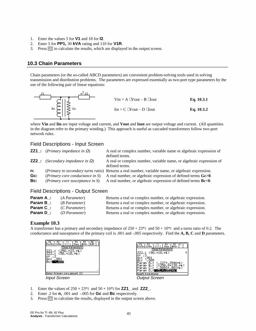
EE Pro for TI -89, 92 PlusAnalysis - Transformer Calculations
41
1. Enter the values 5 for V1 and 18 for I2.2. Enter 5 for PP1, 30 kVA rating and 110 for V1R.3. Press „ to calculate the results, which are displayed in the output screen.
10.3 Chain Parameters
Chain parameters (or the so-called ABCD parameters) are convenient problem-solving tools used in solvingtransmission and distribution problems. The parameters are expressed essentially as two-port type parameters by theuse of the following pair of linear equations:
Vin = A ⋅ Vout – B ⋅ Iout Eq. 10.3.1
Iin = C ⋅ Vout – D ⋅ Iout Eq. 10.3.2
where Vin and Iin are input voltage and current, and Vout and Iout are output voltage and current. (All quantitiesin the diagram refer to the primary winding.) This approach is useful as cascaded transformers follow two-portnetwork rules.
Field Descriptions - Input ScreenZZ1_: (Primary impedance in Ω) A real or complex number, variable name or algebraic expression of
defined terms.ZZ2_: (Secondary impedance in Ω) A real or complex number, variable name, or algebraic expression of
defined terms.n: (Primary to secondary turns ratio) Returns a real number, variable name, or algebraic expression.Gc: (Primary core conductance in S) A real number, or algebraic expression of defined terms Gc>0.Bc : (Primary core susceptance in S) A real number, or algebraic expression of defined terms Bc<0.
Field Descriptions - Output ScreenParam A_ : (A Parameter) Returns a real or complex number, or algebraic expression.Param B_ : (B Parameter) Returns a real or complex number, or algebraic expression.Param C_ : (C Parameter) Returns a real or complex number, or algebraic expression.Param D_ : (D Parameter) Returns a real or complex number, or algebraic expression.
Example 10.3A transformer has a primary and secondary impedance of 250 + 23*i and 50 + 10*i and a turns ratio of 0.2. Theconductance and susceptance of the primary coil is .001 and -.005 respectively. Find the A, B, C and D parameters.
Input Screen Output Screen
1. Enter the values of 250 + 23*i and 50 + 10*i for ZZ1_ and ZZ2_.2. Enter .2 for n, .001 and -.005 for Gc and Bc respectively.3. Press „ to calculate the results, displayed in the output screen above.
Z1 n2·Z2
Bc Gc

EE Pro for TI -89, 92 PlusAnalysis - Transformer Calculations
42
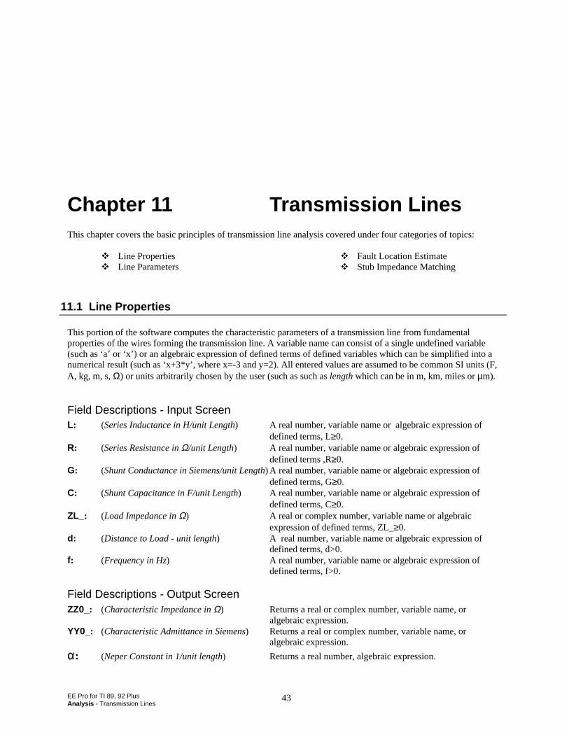
EE Pro for TI 89, 92 PlusAnalysis - Transmission Lines
43
Chapter 11 Transmission LinesThis chapter covers the basic principles of transmission line analysis covered under four categories of topics:
Line PropertiesLine Parameters
Fault Location EstimateStub Impedance Matching
11.1 Line Properties
This portion of the software computes the characteristic parameters of a transmission line from fundamentalproperties of the wires forming the transmission line. A variable name can consist of a single undefined variable(such as ‘a’ or ‘x’) or an algebraic expression of defined terms of defined variables which can be simplified into anumerical result (such as ‘x+3*y’, where x=-3 and y=2). All entered values are assumed to be common SI units (F,A, kg, m, s, Ω) or units arbitrarily chosen by the user (such as such as length which can be in m, km, miles or µm).
Field Descriptions - Input ScreenL: (Series Inductance in H/unit Length) A real number, variable name or algebraic expression of
defined terms, L≥0.R: (Series Resistance in Ω/unit Length) A real number, variable name or algebraic expression of
defined terms ,R≥0.G: (Shunt Conductance in Siemens/unit Length) A real number, variable name or algebraic expression of
defined terms, G≥0.C: (Shunt Capacitance in F/unit Length) A real number, variable name or algebraic expression of
defined terms, C≥0.ZL_: (Load Impedance in Ω) A real or complex number, variable name or algebraic
expression of defined terms, ZL_≥0.d: (Distance to Load - unit length) A real number, variable name or algebraic expression of
defined terms, d>0.f: (Frequency in Hz) A real number, variable name or algebraic expression of
defined terms, f>0.
Field Descriptions - Output ScreenZZ0_: (Characteristic Impedance in Ω) Returns a real or complex number, variable name, or
algebraic expression.YY0_: (Characteristic Admittance in Siemens) Returns a real or complex number, variable name, or
algebraic expression.
αα: (Neper Constant in 1/unit length) Returns a real number, algebraic expression.
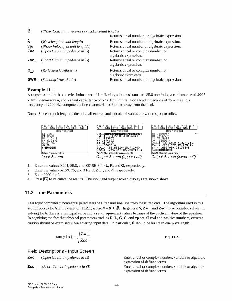
EE Pro for TI 89, 92 PlusAnalysis - Transmission Lines
44
ββ: (Phase Constant in degrees or radians/unit length) Returns a real number, or algebraic expression.
λλ: (Wavelength in unit length) Returns a real number or algebraic expression.vp : (Phase Velocity in unit length/s) Returns a real number or algebraic expression.Zoc_ : (Open Circuit Impedance in Ω) Returns a real or complex number, or
algebraic expression.Zsc_ : (Short Circuit Impedance in Ω) Returns a real or complex number, or
algebraic expression.
ρρ__: (Reflection Coefficient) Returns a real or complex number, oralgebraic expression.
SWR: (Standing Wave Ratio) Returns a real number, or algebraic expression.
Example 11.1A transmission line has a series inductance of 1 mH/mile, a line resistance of 85.8 ohm/mile, a conductance of .0015
x 10-6 Siemens/mile, and a shunt capacitance of 62 x 10-9 F/mile. For a load impedance of 75 ohms and afrequency of 2000 Hz, compute the line characteristics 3 miles away from the load.
Note: Since the unit length is the mile, all entered and calculated values are with respect to miles.
Input Screen Output Screen (upper half) Output Screen (lower half)
1. Enter the values 0.001, 85.8, and .0015E-6 for L, R, and G, respectively.2. Enter the values 62E-9, 75, and 3 for C, ZL_, and d, respectively.3. Enter 2000 for f.4. Press „ to calculate the results. The input and output screen displays are shown above.
11.2 Line Parameters
This topic computes fundamental parameters of a transmission line from measured data. The algorithm used in thissection solves for γ in the equation 11.2.1, where γ = α + jβ. In general γ, Zsc_, and Zoc_ have complex values. Insolving for γ, there is a principal value and a set of equivalent values because of the cyclical nature of the equation.Recognizing the fact that physical parameters such as R, L , G, C, and vp are all real and positive numbers, extremecaution should be exercised when entering input data. In particular, d should be less than one wavelength.
tan( )_
_γ ⋅ =d
Zsc
Zoc Eq. 11.2.1
Field Descriptions - Input ScreenZoc_ : (Open Circuit Impedance in Ω) Enter a real or complex number, variable or algebraic
expression of defined terms.Zsc_ : (Short Circuit Impedance in Ω) Enter a real or complex number, variable or algebraic
expression of defined terms.
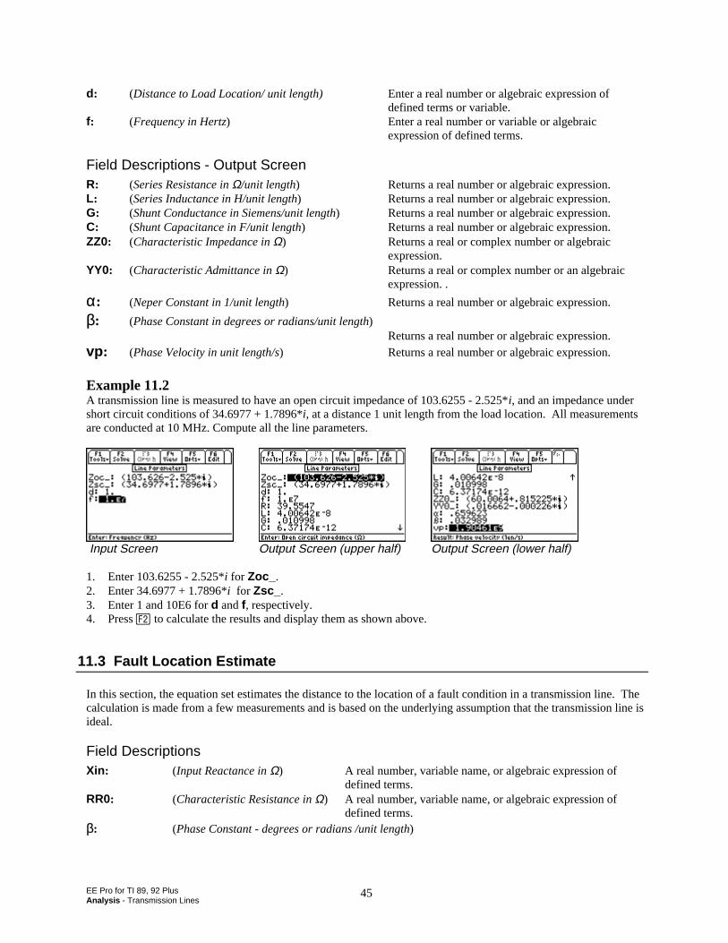
EE Pro for TI 89, 92 PlusAnalysis - Transmission Lines
45
d: (Distance to Load Location/ unit length) Enter a real number or algebraic expression of defined terms or variable.
f: (Frequency in Hertz) Enter a real number or variable or algebraicexpression of defined terms.
Field Descriptions - Output ScreenR: (Series Resistance in Ω/unit length) Returns a real number or algebraic expression.L: (Series Inductance in H/unit length) Returns a real number or algebraic expression.G: (Shunt Conductance in Siemens/unit length) Returns a real number or algebraic expression.C: (Shunt Capacitance in F/unit length) Returns a real number or algebraic expression.ZZ0: (Characteristic Impedance in Ω) Returns a real or complex number or algebraic
expression.YY0: (Characteristic Admittance in Ω) Returns a real or complex number or an algebraic
expression. .
αα: (Neper Constant in 1/unit length) Returns a real number or algebraic expression.
ββ: (Phase Constant in degrees or radians/unit length) Returns a real number or algebraic expression.
vp : (Phase Velocity in unit length/s) Returns a real number or algebraic expression.
Example 11.2A transmission line is measured to have an open circuit impedance of 103.6255 - 2.525*i, and an impedance undershort circuit conditions of 34.6977 + 1.7896*i, at a distance 1 unit length from the load location. All measurementsare conducted at 10 MHz. Compute all the line parameters.
Input Screen Output Screen (upper half) Output Screen (lower half)
1. Enter 103.6255 - 2.525*i for Zoc_ .2. Enter 34.6977 + 1.7896*i for Zsc_ .3. Enter 1 and 10E6 for d and f, respectively.4. Press „ to calculate the results and display them as shown above.
11.3 Fault Location Estimate
In this section, the equation set estimates the distance to the location of a fault condition in a transmission line. Thecalculation is made from a few measurements and is based on the underlying assumption that the transmission line isideal.
Field DescriptionsXin : (Input Reactance in Ω) A real number, variable name, or algebraic expression of
defined terms.RR0: (Characteristic Resistance in Ω) A real number, variable name, or algebraic expression of
defined terms.ββ: (Phase Constant - degrees or radians /unit length)
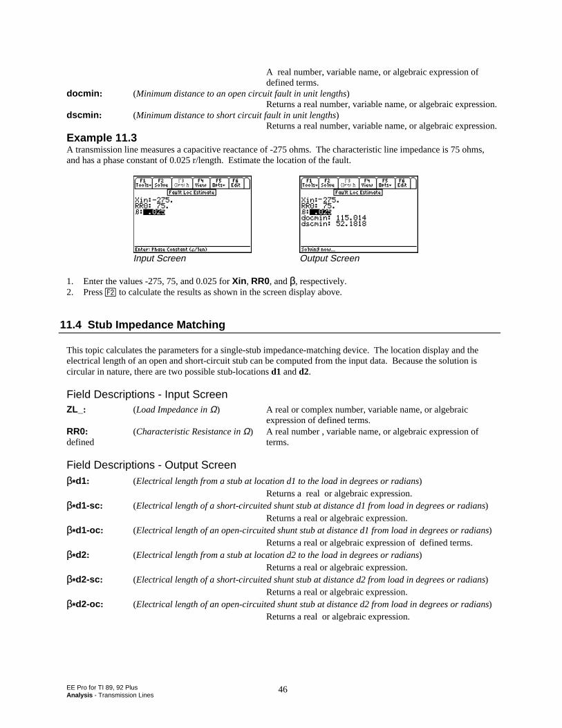
EE Pro for TI 89, 92 PlusAnalysis - Transmission Lines
46
A real number, variable name, or algebraic expression of defined terms.
docmin : (Minimum distance to an open circuit fault in unit lengths)Returns a real number, variable name, or algebraic expression.
dscmin : (Minimum distance to short circuit fault in unit lengths)Returns a real number, variable name, or algebraic expression.
Example 11.3A transmission line measures a capacitive reactance of -275 ohms. The characteristic line impedance is 75 ohms,and has a phase constant of 0.025 r/length. Estimate the location of the fault.
Input Screen Output Screen
1. Enter the values -275, 75, and 0.025 for Xin , RR0, and β, respectively.2. Press „ to calculate the results as shown in the screen display above.
11.4 Stub Impedance Matching
This topic calculates the parameters for a single-stub impedance-matching device. The location display and theelectrical length of an open and short-circuit stub can be computed from the input data. Because the solution iscircular in nature, there are two possible stub-locations d1 and d2.
Field Descriptions - Input ScreenZL_: (Load Impedance in Ω) A real or complex number, variable name, or algebraic
expression of defined terms.RR0: (Characteristic Resistance in Ω) A real number , variable name, or algebraic expression ofdefined terms.
Field Descriptions - Output Screenβ*d1: (Electrical length from a stub at location d1 to the load in degrees or radians)
Returns a real or algebraic expression.β*d1-sc : (Electrical length of a short-circuited shunt stub at distance d1 from load in degrees or radians)
Returns a real or algebraic expression.β*d1-oc : (Electrical length of an open-circuited shunt stub at distance d1 from load in degrees or radians)
Returns a real or algebraic expression of defined terms.β*d2: (Electrical length from a stub at location d2 to the load in degrees or radians)
Returns a real or algebraic expression.β*d2-sc : (Electrical length of a short-circuited shunt stub at distance d2 from load in degrees or radians)
Returns a real or algebraic expression.β*d2-oc : (Electrical length of an open-circuited shunt stub at distance d2 from load in degrees or radians)
Returns a real or algebraic expression.
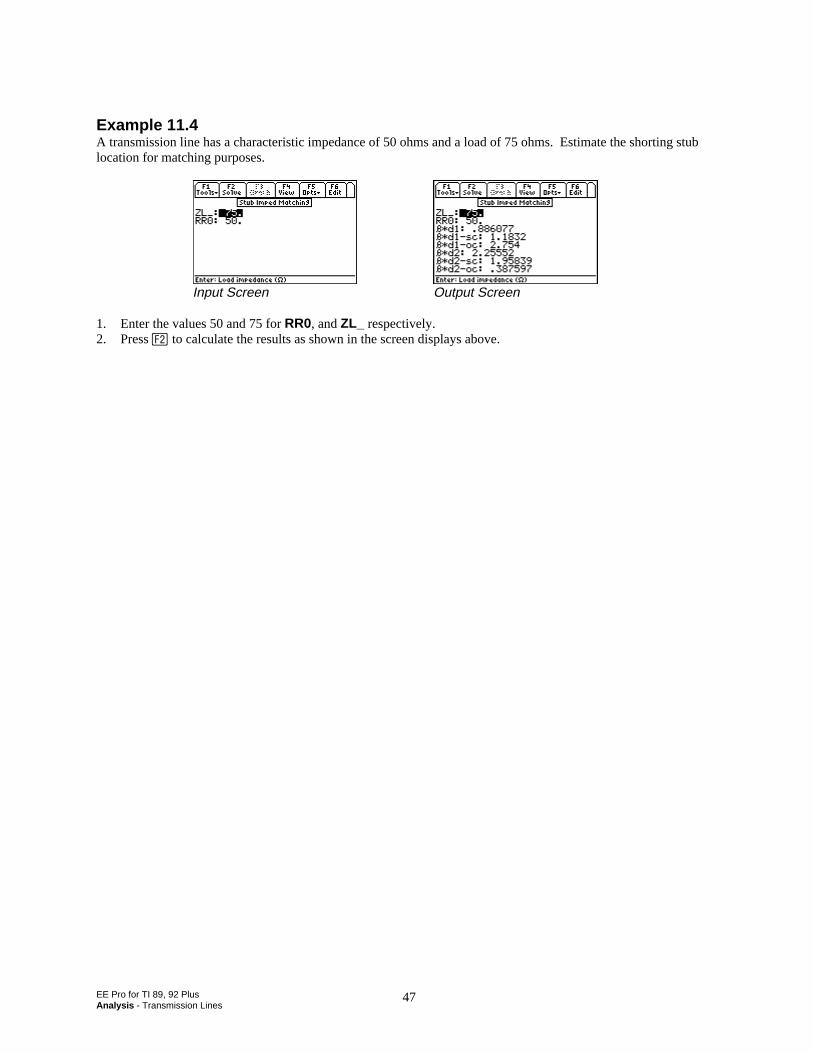
EE Pro for TI 89, 92 PlusAnalysis - Transmission Lines
47
Example 11.4A transmission line has a characteristic impedance of 50 ohms and a load of 75 ohms. Estimate the shorting stublocation for matching purposes.
Input Screen Output Screen
1. Enter the values 50 and 75 for RR0, and ZL_ respectively.2. Press „ to calculate the results as shown in the screen displays above.
EE Pro for TI-89, 92 PlusAnalysis - Computer Engineering
48
Chapter 12 Computer EngineeringThis chapter covers functions of interest in the design of logic systems and circuits. The modules include binaryarithmetic, bit operations, comparisons and a form of logic minimization using the Quine-McCluskey algorithm:
Binary ArithmeticRegister OperationsBit Operations
Binary ConversionsBinary ComparisonsKarnaugh Map
Read This!
The format of integers in the Computer Engineering section of EE•Pro is (p)nnnn…, where p is the letter prefix b,o, d, or h indicating binary, octal, decimal, and hexadecimal, number systems and n represents the legal digits forthe number base. If a number does not begin with a letter prefix in parenthesis, then it is assumed to be in thenumber base set in the †/Modes dialog. With the exception of Binary Conversion, no numbers with fraction
components are allowed to be entered. The TI-89 built-in binary conversion feature supports 32 bit word lengths.EE•Pro has extended this feature to allow the user to modify the word size between 1 and 128 bits.
12.1 Special Mode Settings, the † Key
The screen allows the user to set the parameters for solving binary problems. Press the † key to display a user
interface dialog box prompting the user to clarify and specify the foundation for digital arithmetic. Digitalarithmetic operations are allowed in binary, octal, decimal and hexadecimal number systems. As shown in thescreen display below, user input is needed in the following areas:
Base: Binary, Octal, Decimal and Hexadecimal.Word size: Up to 128 bits.Sign: Unsigned, 1’s complement and 2’s complement techniques.
The software allows three conventions for representing numbers.
1. Unsigned mode - In the unsigned mode, the most significant bit adds magnitude and not the sign to thenumber.
2. 1's Complement mode - One's complement accommodates an equal number of positive and negativenumbers, but has two representations for zero; 0 and -0.
3. 2's complement mode - There is just one representation for zero, but there is always one morenegative number than a positive number represented.
Leading 0's are used for internal representation, but are not displayed as such.Thus a number entered as 000110011 will be displayed as 110011
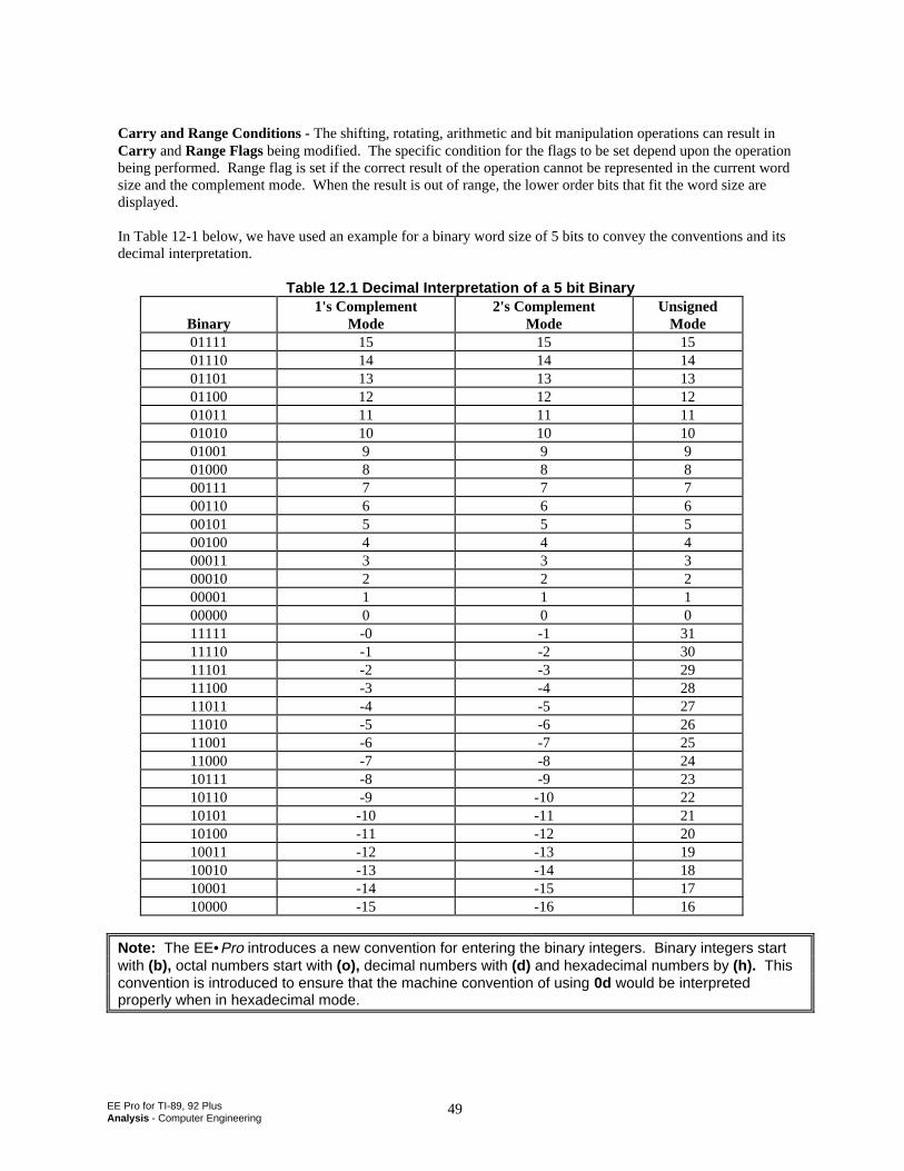
EE Pro for TI-89, 92 PlusAnalysis - Computer Engineering
49
Carry and Range Conditions - The shifting, rotating, arithmetic and bit manipulation operations can result inCarry and Range Flags being modified. The specific condition for the flags to be set depend upon the operationbeing performed. Range flag is set if the correct result of the operation cannot be represented in the current wordsize and the complement mode. When the result is out of range, the lower order bits that fit the word size aredisplayed.
In Table 12-1 below, we have used an example for a binary word size of 5 bits to convey the conventions and itsdecimal interpretation.
Table 12.1 Decimal Interpretation of a 5 bit Binary
Binary1's Complement
Mode2's Complement
ModeUnsigned
Mode01111 15 15 1501110 14 14 1401101 13 13 1301100 12 12 1201011 11 11 1101010 10 10 1001001 9 9 901000 8 8 800111 7 7 700110 6 6 600101 5 5 500100 4 4 400011 3 3 300010 2 2 200001 1 1 100000 0 0 011111 -0 -1 3111110 -1 -2 3011101 -2 -3 2911100 -3 -4 2811011 -4 -5 2711010 -5 -6 2611001 -6 -7 2511000 -7 -8 2410111 -8 -9 2310110 -9 -10 2210101 -10 -11 2110100 -11 -12 2010011 -12 -13 1910010 -13 -14 1810001 -14 -15 1710000 -15 -16 16
Note: The EE•Pro introduces a new convention for entering the binary integers. Binary integers startwith (b), octal numbers start with (o), decimal numbers with (d) and hexadecimal numbers by (h). Thisconvention is introduced to ensure that the machine convention of using 0d would be interpretedproperly when in hexadecimal mode.
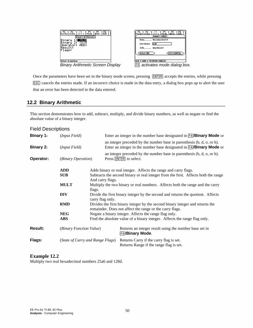
EE Pro for TI-89, 92 PlusAnalysis - Computer Engineering
50
Binary Arithmetic Screen Display † activates mode dialog box.
Once the parameters have been set in the binary mode screen, pressing ¸ accepts the entries, while pressing
N cancels the entries made. If an incorrect choice is made in the data entry, a dialog box pops up to alert the user
that an error has been detected in the data entered.
12.2 Binary Arithmetic
This section demonstrates how to add, subtract, multiply, and divide binary numbers, as well as negate or find theabsolute value of a binary integer.
Field DescriptionsBinary 1 : (Input Field) Enter an integer in the number base designated in †/Binary Mode or
an integer preceded by the number base in parenthesis (b, d, o, or h).Binary 2 : (Input Field) Enter an integer in the number base designated in †/Binary Mode or
an integer preceded by the number base in parenthesis (b, d, o, or h).Operator : (Binary Operation) Press to select.
ADD Adds binary or real integer. Affects the range and carry flags.SUB Subtracts the second binary or real integer from the first. Affects both the range
And carry flags.MULT Multiply the two binary or real numbers. Affects both the range and the carry
flags.DIV Divide the first binary integer by the second and returns the quotient. Affects
carry flag only.RMD Divides the first binary integer by the second binary integer and returns the
remainder. Does not affect the range or the carry flags.NEG Negate a binary integer. Affects the range flag only.ABS Find the absolute value of a binary integer. Affects the range flag only.
Result: (Binary Function Value) Returns an integer result using the number base set in †/Binary Mode .
Flags: (State of Carry and Range Flags) Returns Carry if the carry flag is set.Returns Range if the range flag is set.
Example 12.2Multiply two real hexadecimal numbers 25a6 and 128d.
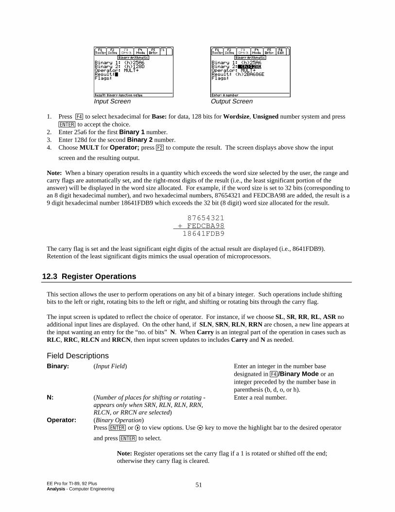
EE Pro for TI-89, 92 PlusAnalysis - Computer Engineering
51
Input Screen Output Screen
1. Press † to select hexadecimal for Base: for data, 128 bits for Wordsize, Unsigned number system and press¸ to accept the choice.
2. Enter 25a6 for the first Binary 1 number.3. Enter 128d for the second Binary 2 number.4. Choose MULT for Operator; press „ to compute the result. The screen displays above show the input
screen and the resulting output.
Note: When a binary operation results in a quantity which exceeds the word size selected by the user, the range andcarry flags are automatically set, and the right-most digits of the result (i.e., the least significant portion of theanswer) will be displayed in the word size allocated. For example, if the word size is set to 32 bits (corresponding toan 8 digit hexadecimal number), and two hexadecimal numbers, 87654321 and FEDCBA98 are added, the result is a9 digit hexadecimal number 18641FDB9 which exceeds the 32 bit (8 digit) word size allocated for the result.
87654321 + FEDCBA98 18641FDB9
The carry flag is set and the least significant eight digits of the actual result are displayed (i.e., 8641FDB9).Retention of the least significant digits mimics the usual operation of microprocessors.
12.3 Register Operations
This section allows the user to perform operations on any bit of a binary integer. Such operations include shiftingbits to the left or right, rotating bits to the left or right, and shifting or rotating bits through the carry flag.
The input screen is updated to reflect the choice of operator. For instance, if we choose SL, SR, RR, RL , ASR noadditional input lines are displayed. On the other hand, if SLN, SRN, RLN , RRN are chosen, a new line appears atthe input wanting an entry for the “no. of bits” N. When Carry is an integral part of the operation in cases such asRLC , RRC, RLCN and RRCN, then input screen updates to includes Carry and N as needed.
Field DescriptionsBinary : (Input Field) Enter an integer in the number base
designated in †/Binary Mode or an integer preceded by the number base in parenthesis (b, d, o, or h).
N: (Number of places for shifting or rotating - Enter a real number.appears only when SRN, RLN, RLN, RRN,RLCN, or RRCN are selected)
Operator: (Binary Operation)Press or B to view options. Use D key to move the highlight bar to the desired operator
and press to select.
Note: Register operations set the carry flag if a 1 is rotated or shifted off the end;otherwise they carry flag is cleared.
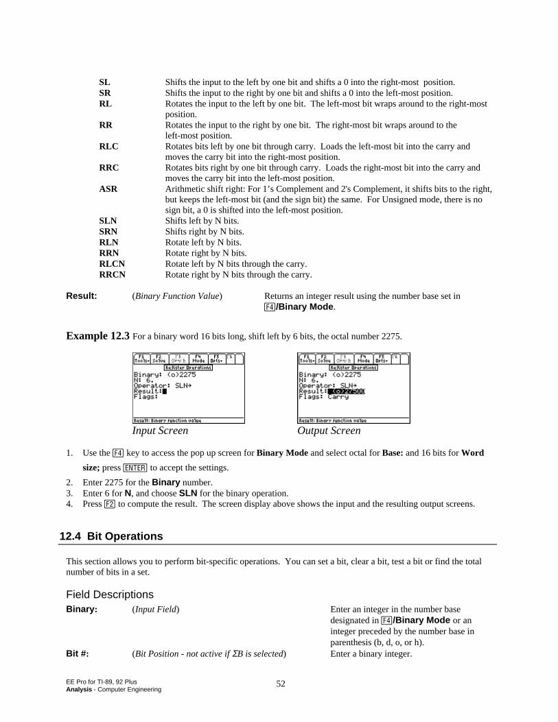
EE Pro for TI-89, 92 PlusAnalysis - Computer Engineering
52
SL Shifts the input to the left by one bit and shifts a 0 into the right-most position.SR Shifts the input to the right by one bit and shifts a 0 into the left-most position.RL Rotates the input to the left by one bit. The left-most bit wraps around to the right-most
position.RR Rotates the input to the right by one bit. The right-most bit wraps around to the
left-most position.RLC Rotates bits left by one bit through carry. Loads the left-most bit into the carry and
moves the carry bit into the right-most position.RRC Rotates bits right by one bit through carry. Loads the right-most bit into the carry and
moves the carry bit into the left-most position.ASR Arithmetic shift right: For 1’s Complement and 2's Complement, it shifts bits to the right,
but keeps the left-most bit (and the sign bit) the same. For Unsigned mode, there is nosign bit, a 0 is shifted into the left-most position.
SLN Shifts left by N bits.SRN Shifts right by N bits.RLN Rotate left by N bits.RRN Rotate right by N bits.RLCN Rotate left by N bits through the carry.RRCN Rotate right by N bits through the carry.
Result: (Binary Function Value) Returns an integer result using the number base set in †/Binary Mode .
Example 12.3 For a binary word 16 bits long, shift left by 6 bits, the octal number 2275.
Input Screen Output Screen
1. Use the † key to access the pop up screen for Binary Mode and select octal for Base: and 16 bits for Word
size; press to accept the settings.
2. Enter 2275 for the Binary number.3. Enter 6 for N, and choose SLN for the binary operation.4. Press „ to compute the result. The screen display above shows the input and the resulting output screens.
12.4 Bit Operations
This section allows you to perform bit-specific operations. You can set a bit, clear a bit, test a bit or find the totalnumber of bits in a set.
Field DescriptionsBinary : (Input Field) Enter an integer in the number base
designated in †/Binary Mode or an integer preceded by the number base in parenthesis (b, d, o, or h).
Bit # : (Bit Position - not active if ΣB is selected) Enter a binary integer.
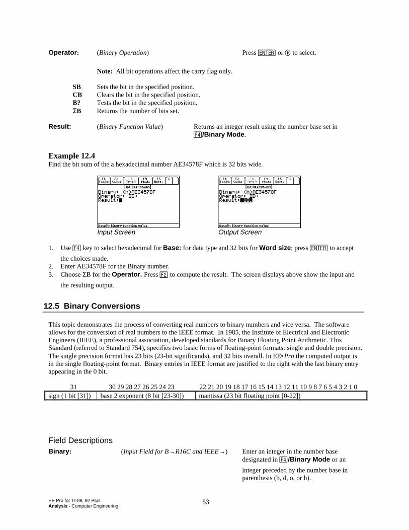
EE Pro for TI-89, 92 PlusAnalysis - Computer Engineering
53
Operator : (Binary Operation) Press or B to select.
Note: All bit operations affect the carry flag only.
SB Sets the bit in the specified position.CB Clears the bit in the specified position.B? Tests the bit in the specified position.ΣB Returns the number of bits set.
Result: (Binary Function Value) Returns an integer result using the number base set in †/Binary Mode .
Example 12.4Find the bit sum of the a hexadecimal number AE34578F which is 32 bits wide.
Input Screen Output Screen
1. Use † key to select hexadecimal for Base: for data type and 32 bits for Word size ; press to accept
the choices made.2. Enter AE34578F for the Binary number.3. Choose ΣB for the Operator. Press „ to compute the result. The screen displays above show the input and
the resulting output.
12.5 Binary Conversions
This topic demonstrates the process of converting real numbers to binary numbers and vice versa. The softwareallows for the conversion of real numbers to the IEEE format. In 1985, the Institute of Electrical and ElectronicEngineers (IEEE), a professional association, developed standards for Binary Floating Point Arithmetic. ThisStandard (referred to Standard 754), specifies two basic forms of floating-point formats: single and double precision.The single precision format has 23 bits (23-bit significands), and 32 bits overall. In EE•Pro the computed output isin the single floating-point format. Binary entries in IEEE format are justified to the right with the last binary entryappearing in the 0 bit.
31 30 29 28 27 26 25 24 23 22 21 20 19 18 17 16 15 14 13 12 11 10 9 8 7 6 5 4 3 2 1 0sign (1 bit [31]) base 2 exponent (8 bit [23-30]) mantissa (23 bit floating point [0-22])
Field DescriptionsBinary : (Input Field for B→R16C and IEEE→) Enter an integer in the number base
designated in †/Binary Mode or an
integer preceded by the number base in parenthesis (b, d, o, or h).
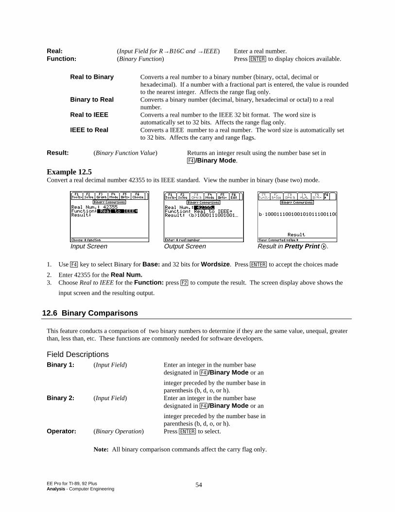
EE Pro for TI-89, 92 PlusAnalysis - Computer Engineering
54
Real: (Input Field for R→B16C and →IEEE) Enter a real number.Function : (Binary Function) Press to display choices available.
Real to Binary Converts a real number to a binary number (binary, octal, decimal orhexadecimal). If a number with a fractional part is entered, the value is rounded to the nearest integer. Affects the range flag only.
Binary to Real Converts a binary number (decimal, binary, hexadecimal or octal) to a realnumber.
Real to IEEE Converts a real number to the IEEE 32 bit format. The word size isautomatically set to 32 bits. Affects the range flag only.
IEEE to Real Converts a IEEE number to a real number. The word size is automatically setto 32 bits. Affects the carry and range flags.
Result: (Binary Function Value) Returns an integer result using the number base set in †/Binary Mode .
Example 12.5Convert a real decimal number 42355 to its IEEE standard. View the number in binary (base two) mode.
Input Screen Output Screen Result in Pretty Print B.
1. Use † key to select Binary for Base : and 32 bits for Wordsize . Press to accept the choices made
2. Enter 42355 for the Real Num. 3. Choose Real to IEEE for the Function: press „ to compute the result. The screen display above shows the
input screen and the resulting output.
12.6 Binary Comparisons
This feature conducts a comparison of two binary numbers to determine if they are the same value, unequal, greaterthan, less than, etc. These functions are commonly needed for software developers.
Field DescriptionsBinary 1 : (Input Field) Enter an integer in the number base
designated in †/Binary Mode or an
integer preceded by the number base in parenthesis (b, d, o, or h).
Binary 2 : (Input Field) Enter an integer in the number base designated in †/Binary Mode or an
integer preceded by the number base in parenthesis (b, d, o, or h).
Operator : (Binary Operation) Press to select.
Note: All binary comparison commands affect the carry flag only.
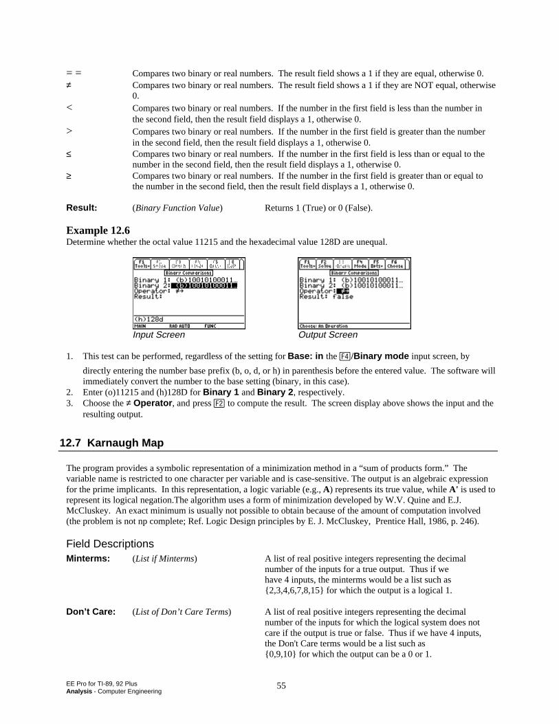
EE Pro for TI-89, 92 PlusAnalysis - Computer Engineering
55
= = Compares two binary or real numbers. The result field shows a 1 if they are equal, otherwise 0.≠ Compares two binary or real numbers. The result field shows a 1 if they are NOT equal, otherwise
0. < Compares two binary or real numbers. If the number in the first field is less than the number in
the second field, then the result field displays a 1, otherwise 0. > Compares two binary or real numbers. If the number in the first field is greater than the number
in the second field, then the result field displays a 1, otherwise 0.≤ Compares two binary or real numbers. If the number in the first field is less than or equal to the
number in the second field, then the result field displays a 1, otherwise 0.≥ Compares two binary or real numbers. If the number in the first field is greater than or equal to
the number in the second field, then the result field displays a 1, otherwise 0.
Result : (Binary Function Value) Returns 1 (True) or 0 (False).
Example 12.6Determine whether the octal value 11215 and the hexadecimal value 128D are unequal.
Input Screen Output Screen
1. This test can be performed, regardless of the setting for Base: in the †/Binary mode input screen, by
directly entering the number base prefix (b, o, d, or h) in parenthesis before the entered value. The software willimmediately convert the number to the base setting (binary, in this case).
2. Enter (o)11215 and (h)128D for Binary 1 and Binary 2 , respectively.3. Choose the ≠ Operator , and press „ to compute the result. The screen display above shows the input and the
resulting output.
12.7 Karnaugh Map
The program provides a symbolic representation of a minimization method in a “sum of products form.” Thevariable name is restricted to one character per variable and is case-sensitive. The output is an algebraic expressionfor the prime implicants. In this representation, a logic variable (e.g., A) represents its true value, while A' is used torepresent its logical negation.The algorithm uses a form of minimization developed by W.V. Quine and E.J.McCluskey. An exact minimum is usually not possible to obtain because of the amount of computation involved(the problem is not np complete; Ref. Logic Design principles by E. J. McCluskey, Prentice Hall, 1986, p. 246).
Field DescriptionsMinterms: (List if Minterms) A list of real positive integers representing the decimal
number of the inputs for a true output. Thus if wehave 4 inputs, the minterms would be a list such as2,3,4,6,7,8,15 for which the output is a logical 1.
Don’t Care: (List of Don’t Care Terms) A list of real positive integers representing the decimalnumber of the inputs for which the logical system does notcare if the output is true or false. Thus if we have 4 inputs,the Don't Care terms would be a list such as0,9,10 for which the output can be a 0 or 1.
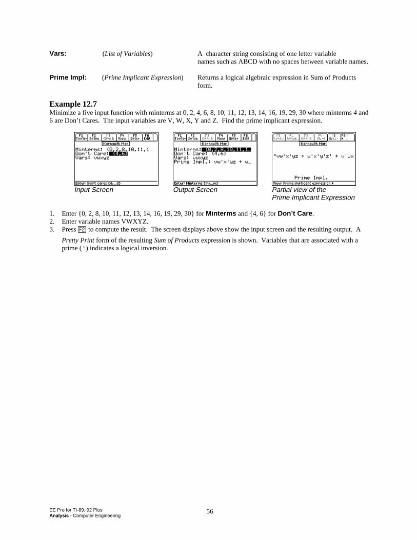
EE Pro for TI-89, 92 PlusAnalysis - Computer Engineering
56
Vars: (List of Variables) A character string consisting of one letter variable names such as ABCD with no spaces between variable names.
Prime Impl: (Prime Implicant Expression) Returns a logical algebraic expression in Sum of Productsform.
Example 12.7Minimize a five input function with minterms at 0, 2, 4, 6, 8, 10, 11, 12, 13, 14, 16, 19, 29, 30 where minterms 4 and6 are Don’t Cares. The input variables are V, W, X, Y and Z. Find the prime implicant expression.
Input Screen Output Screen Partial view of thePrime Implicant Expression
1. Enter 0, 2, 8, 10, 11, 12, 13, 14, 16, 19, 29, 30 for Minterms and 4, 6 for Don’t Care .2. Enter variable names VWXYZ.3. Press „ to compute the result. The screen displays above show the input screen and the resulting output. A
Pretty Print form of the resulting Sum of Products expression is shown. Variables that are associated with aprime (‘ ) indicates a logical inversion.
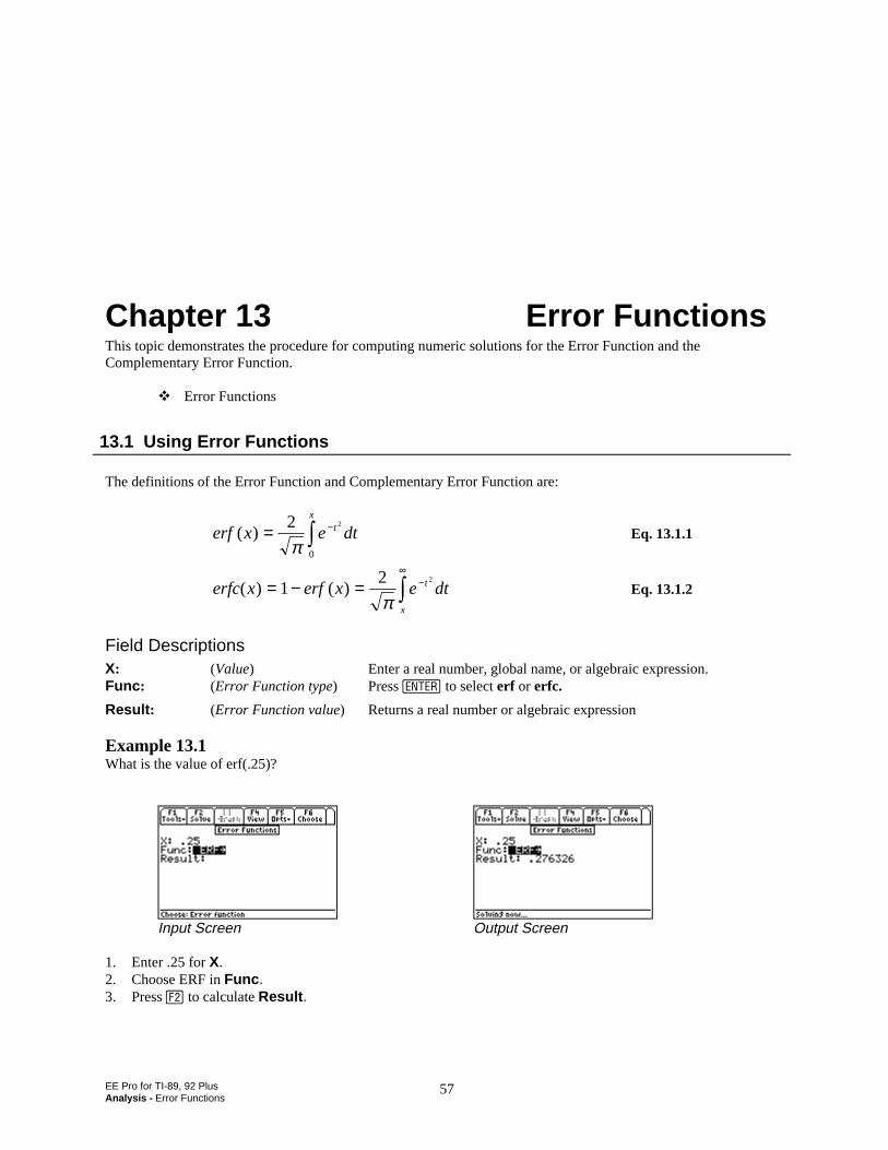
EE Pro for TI-89, 92 PlusAnalysis - Error Functions
57
Chapter 13 Error FunctionsThis topic demonstrates the procedure for computing numeric solutions for the Error Function and theComplementary Error Function.
Error Functions
13.1 Using Error Functions
The definitions of the Error Function and Complementary Error Function are:
erf x e dttx
( ) = −z2 2
0πEq. 13.1.1
erfc x erf x e dtt
x
( ) ( )= − = −∞
z12 2
πEq. 13.1.2
Field DescriptionsX: (Value) Enter a real number, global name, or algebraic expression.Func : (Error Function type) Press to select erf or erfc.
Result : (Error Function value) Returns a real number or algebraic expression
Example 13.1What is the value of erf(.25)?
Input Screen Output Screen
1. Enter .25 for X.2. Choose ERF in Func .3. Press „ to calculate Result .
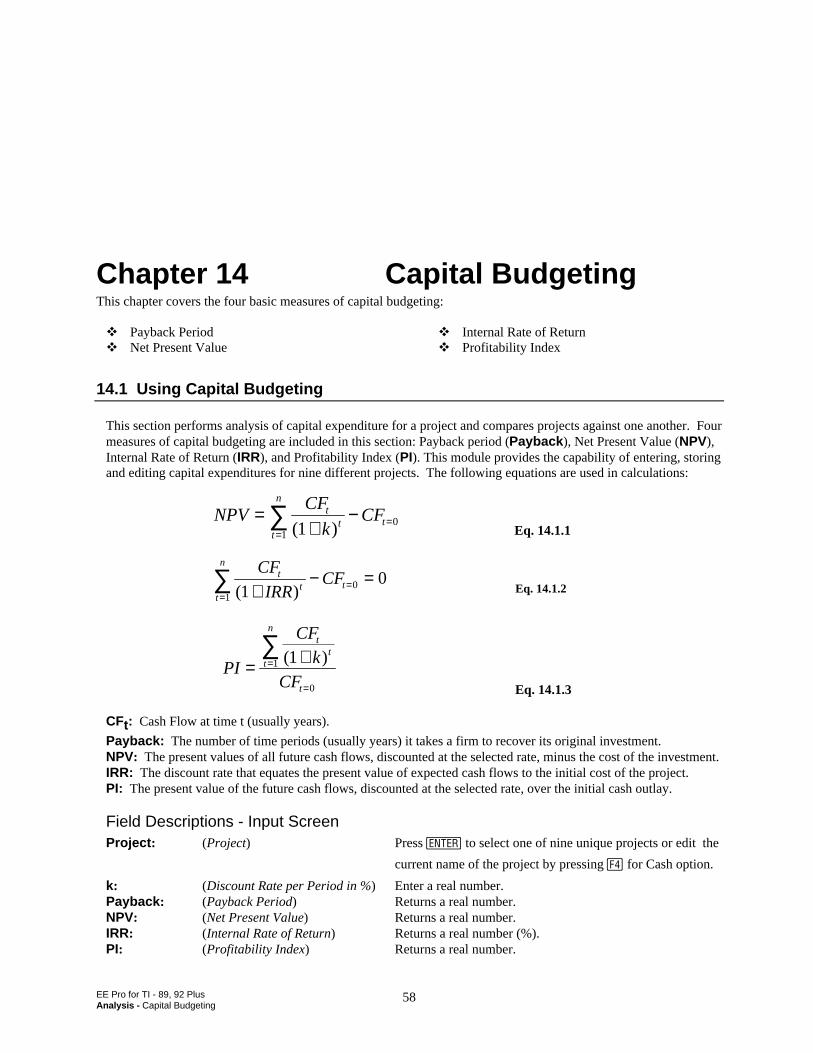
EE Pro for TI - 89, 92 PlusAnalysis - Capital Budgeting
58
Chapter 14 Capital BudgetingThis chapter covers the four basic measures of capital budgeting:
Payback PeriodNet Present Value
Internal Rate of ReturnProfitability Index
14.1 Using Capital Budgeting
This section performs analysis of capital expenditure for a project and compares projects against one another. Fourmeasures of capital budgeting are included in this section: Payback period (Payback ), Net Present Value (NPV),Internal Rate of Return (IRR), and Profitability Index (PI). This module provides the capability of entering, storingand editing capital expenditures for nine different projects. The following equations are used in calculations:
Eq. 14.1.1
Eq. 14.1.2
Eq. 14.1.3
CFt: Cash Flow at time t (usually years).
Payback: The number of time periods (usually years) it takes a firm to recover its original investment.NPV: The present values of all future cash flows, discounted at the selected rate, minus the cost of the investment.IRR: The discount rate that equates the present value of expected cash flows to the initial cost of the project.PI: The present value of the future cash flows, discounted at the selected rate, over the initial cash outlay.
Field Descriptions - Input ScreenProject : (Project) Press to select one of nine unique projects or edit the
current name of the project by pressing † for Cash option.
k: (Discount Rate per Period in %) Enter a real number.Payback : (Payback Period) Returns a real number.NPV: (Net Present Value) Returns a real number.IRR: (Internal Rate of Return) Returns a real number (%).PI: (Profitability Index) Returns a real number.
NPVCF
kCFt
tt
n
t=+
−=
=∑ ( )110
CF
IRRCFt
t tt
n
( )100
1 +− ==
=∑
PI
CF
kCF
tt
t
n
t
= +=
=
∑ ( )11
0
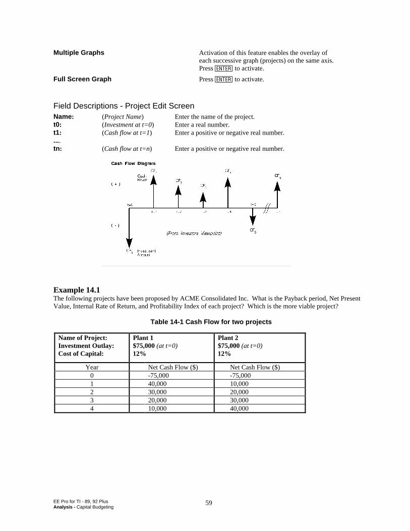
EE Pro for TI - 89, 92 PlusAnalysis - Capital Budgeting
59
Multiple Graphs Activation of this feature enables the overlay of each successive graph (projects) on the same axis.Press to activate.
Full Screen Graph Press to activate.
Field Descriptions - Project Edit ScreenName: (Project Name) Enter the name of the project.t0: (Investment at t=0) Enter a real number.t1: (Cash flow at t=1) Enter a positive or negative real number.....tn : (Cash flow at t=n) Enter a positive or negative real number.
Example 14.1The following projects have been proposed by ACME Consolidated Inc. What is the Payback period, Net PresentValue, Internal Rate of Return, and Profitability Index of each project? Which is the more viable project?
Table 14-1 Cash Flow for two projects
Name of Project: Plant 1 Plant 2Investment Outlay: $75,000 (at t=0) $75,000 (at t=0)Cost of Capital: 12% 12%
Year Net Cash Flow ($) Net Cash Flow ($)0 -75,000 -75,0001 40,000 10,0002 30,000 20,0003 20,000 30,0004 10,000 40,000
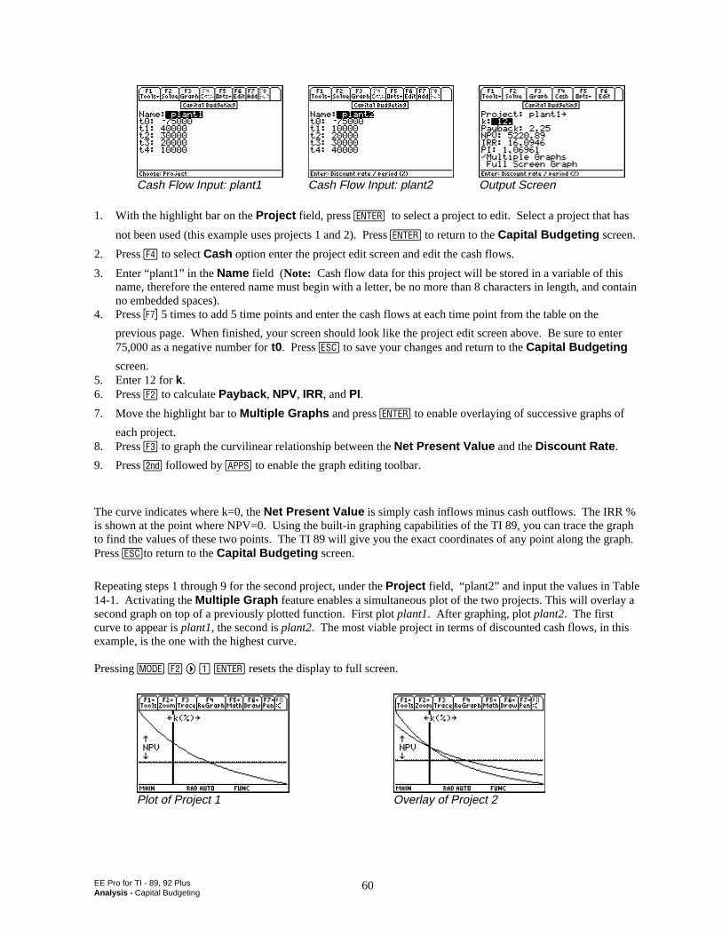
EE Pro for TI - 89, 92 PlusAnalysis - Capital Budgeting
60
Cash Flow Input: plant1 Cash Flow Input: plant2 Output Screen
1. With the highlight bar on the Project field, press to select a project to edit. Select a project that has
not been used (this example uses projects 1 and 2). Press ¸ to return to the Capital Budgeting screen.
2. Press † to select Cash option enter the project edit screen and edit the cash flows.
3. Enter “plant1” in the Name field (Note: Cash flow data for this project will be stored in a variable of thisname, therefore the entered name must begin with a letter, be no more than 8 characters in length, and containno embedded spaces).
4. Press ‰ 5 times to add 5 time points and enter the cash flows at each time point from the table on the
previous page. When finished, your screen should look like the project edit screen above. Be sure to enter75,000 as a negative number for t0. Press N to save your changes and return to the Capital Budgeting
screen.5. Enter 12 for k.6. Press „ to calculate Payback , NPV, IRR, and PI.
7. Move the highlight bar to Multiple Graphs and press to enable overlaying of successive graphs of
each project.8. Press … to graph the curvilinear relationship between the Net Present Value and the Discount Rate .
9. Press 2 followed by O to enable the graph editing toolbar.
The curve indicates where k=0, the Net Present Value is simply cash inflows minus cash outflows. The IRR %is shown at the point where NPV=0. Using the built-in graphing capabilities of the TI 89, you can trace the graphto find the values of these two points. The TI 89 will give you the exact coordinates of any point along the graph.Press Nto return to the Capital Budgeting screen.
Repeating steps 1 through 9 for the second project, under the Project field, “plant2” and input the values in Table14-1. Activating the Multiple Graph feature enables a simultaneous plot of the two projects. This will overlay asecond graph on top of a previously plotted function. First plot plant1. After graphing, plot plant2. The firstcurve to appear is plant1, the second is plant2. The most viable project in terms of discounted cash flows, in thisexample, is the one with the highest curve.
Pressing 3 „ B ¨ ¸ resets the display to full screen.
Plot of Project 1 Overlay of Project 2
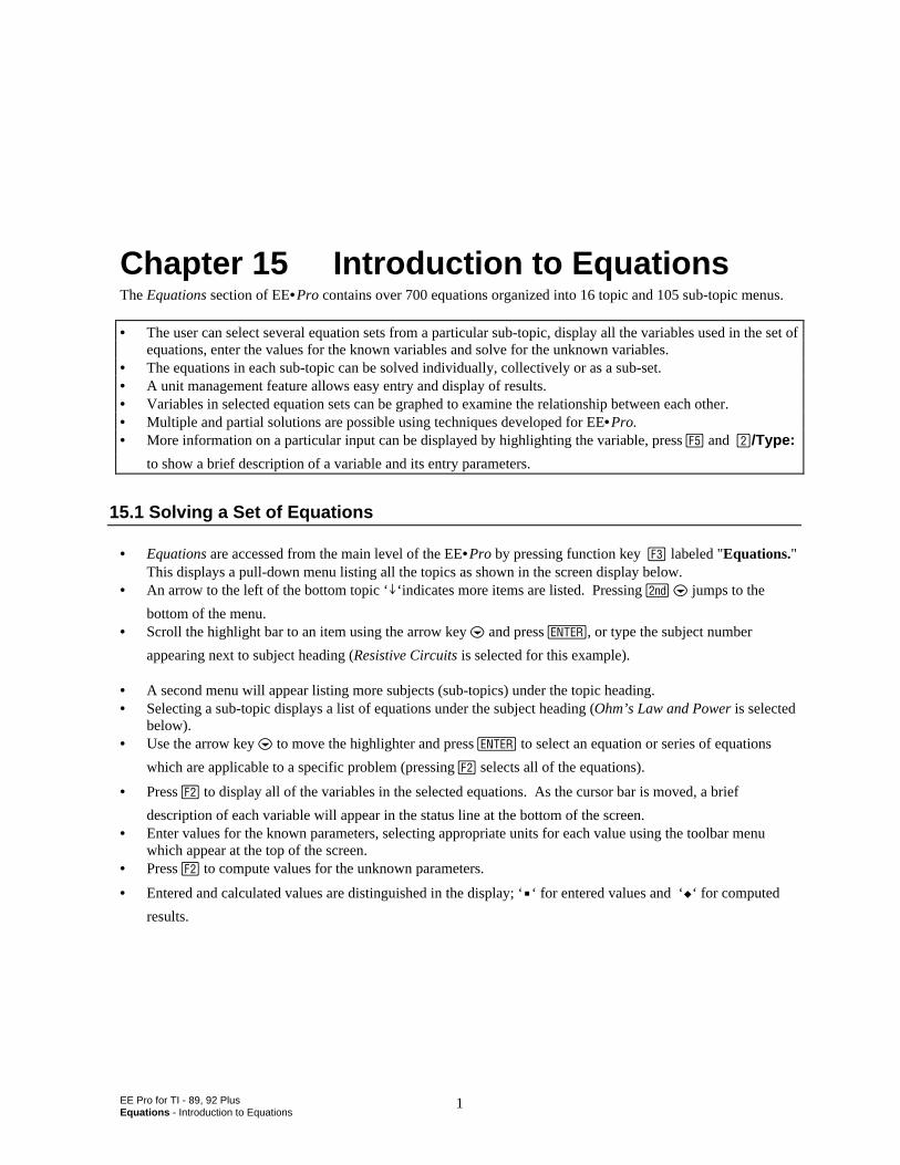
EE Pro for TI - 89, 92 PlusEquations - Introduction to Equations
1
Chapter 15 Introduction to EquationsThe Equations section of EE•Pro contains over 700 equations organized into 16 topic and 105 sub-topic menus.
• The user can select several equation sets from a particular sub-topic, display all the variables used in the set ofequations, enter the values for the known variables and solve for the unknown variables.
• The equations in each sub-topic can be solved individually, collectively or as a sub-set.• A unit management feature allows easy entry and display of results.• Variables in selected equation sets can be graphed to examine the relationship between each other.• Multiple and partial solutions are possible using techniques developed for EE•Pro.• More information on a particular input can be displayed by highlighting the variable, press ‡ and ©/Type:
to show a brief description of a variable and its entry parameters.
15.1 Solving a Set of Equations
• Equations are accessed from the main level of the EE•Pro by pressing function key … labeled "Equations."This displays a pull-down menu listing all the topics as shown in the screen display below.
• An arrow to the left of the bottom topic ‘ï‘indicates more items are listed. Pressing 2 D jumps to the
bottom of the menu.• Scroll the highlight bar to an item using the arrow key D and press , or type the subject number
appearing next to subject heading (Resistive Circuits is selected for this example).
• A second menu will appear listing more subjects (sub-topics) under the topic heading.• Selecting a sub-topic displays a list of equations under the subject heading (Ohm’s Law and Power is selected
below).• Use the arrow key D to move the highlighter and press to select an equation or series of equations
which are applicable to a specific problem (pressing „ selects all of the equations).
• Press „ to display all of the variables in the selected equations. As the cursor bar is moved, a brief
description of each variable will appear in the status line at the bottom of the screen.• Enter values for the known parameters, selecting appropriate units for each value using the toolbar menu
which appear at the top of the screen.• Press „ to compute values for the unknown parameters.
• Entered and calculated values are distinguished in the display; ‘é‘ for entered values and ‘‘ for computed
results.
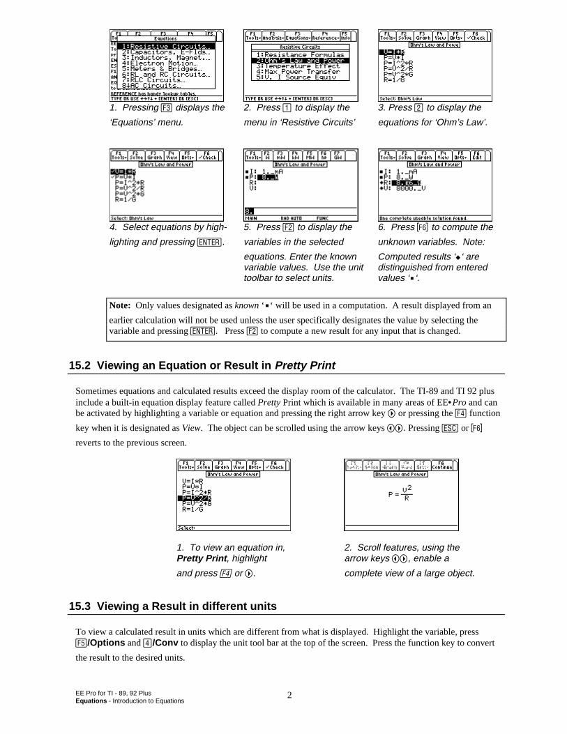
EE Pro for TI - 89, 92 PlusEquations - Introduction to Equations
2
1. Pressing … displays the 2. Press ¨ to display the 3. Press © to display the
‘Equations’ menu. menu in ‘Resistive Circuits’ equations for ‘Ohm’s Law’.
4. Select equations by high- 5. Press „ to display the 6. Press ˆ to compute the
lighting and pressing ¸. variables in the selected unknown variables. Note:
equations. Enter the known Computed results ‘‘ are variable values. Use the unit distinguished from entered toolbar to select units. values ‘é‘.
Note: Only values designated as known ‘é‘ will be used in a computation. A result displayed from an
earlier calculation will not be used unless the user specifically designates the value by selecting thevariable and pressing . Press „ to compute a new result for any input that is changed.
15.2 Viewing an Equation or Result in Pretty Print
Sometimes equations and calculated results exceed the display room of the calculator. The TI-89 and TI 92 plusinclude a built-in equation display feature called Pretty Print which is available in many areas of EE•Pro and canbe activated by highlighting a variable or equation and pressing the right arrow key B or pressing the † function
key when it is designated as View. The object can be scrolled using the arrow keys AB. Pressing N or
reverts to the previous screen.
1. To view an equation in, 2. Scroll features, using the
Pretty Print , highlight arrow keys AB, enable a
and press † or B. complete view of a large object.
15.3 Viewing a Result in different units
To view a calculated result in units which are different from what is displayed. Highlight the variable, press‡/Options and y/Conv to display the unit tool bar at the top of the screen. Press the function key to convert
the result to the desired units.
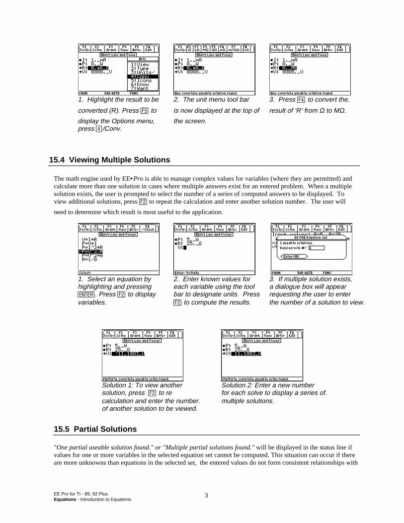
EE Pro for TI - 89, 92 PlusEquations - Introduction to Equations
3
1. Highlight the result to be 2. The unit menu tool bar 3. Press † to convert the.
converted (R). Press ‡ to is now displayed at the top of result of ‘R’ from Ω to MΩ.
display the Options menu, the screen. press y/Conv.
15.4 Viewing Multiple Solutions
The math engine used by EE•Pro is able to manage complex values for variables (where they are permitted) andcalculate more than one solution in cases where multiple answers exist for an entered problem. When a multiplesolution exists, the user is prompted to select the number of a series of computed answers to be displayed. Toview additional solutions, press „ to repeat the calculation and enter another solution number. The user will
need to determine which result is most useful to the application.
1. Select an equation by 2. Enter known values for 3. If multiple solution exists, highlighting and pressing each variable using the tool a dialogue box will appear ¸. Press „ to display bar to designate units. Press requesting the user to enter variables. „ to compute the results. the number of a solution to view.
Solution 1: To view another Solution 2: Enter a new number solution, press „ to re for each solve to display a series of. calculation and enter the number. multiple solutions. of another solution to be viewed.
15.5 Partial Solutions
"One partial useable solution found." or "Multiple partial solutions found." will be displayed in the status line ifvalues for one or more variables in the selected equation set cannot be computed. This situation can occur if thereare more unknowns than equations in the selected set, the entered values do not form consistent relationships with
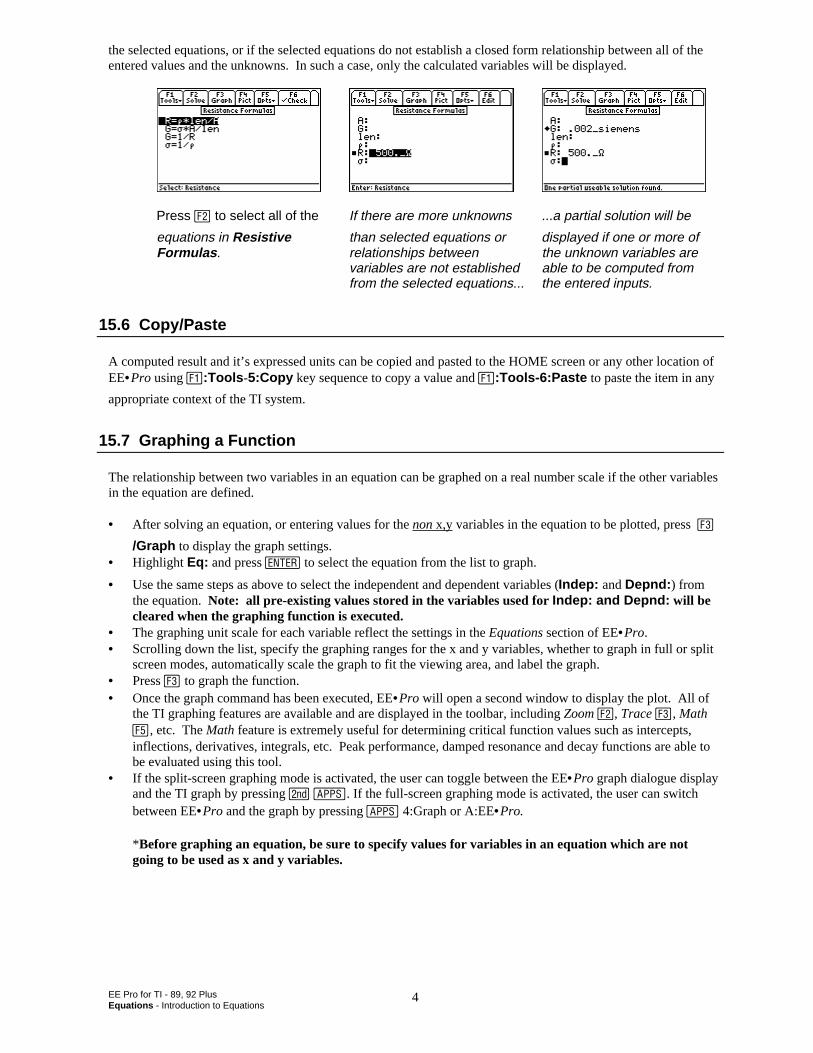
EE Pro for TI - 89, 92 PlusEquations - Introduction to Equations
4
the selected equations, or if the selected equations do not establish a closed form relationship between all of theentered values and the unknowns. In such a case, only the calculated variables will be displayed.
Press „ to select all of the If there are more unknowns ...a partial solution will be
equations in Resistive than selected equations or displayed if one or more of Formulas . relationships between the unknown variables are
variables are not established able to be computed from from the selected equations... the entered inputs.
15.6 Copy/Paste
A computed result and it’s expressed units can be copied and pasted to the HOME screen or any other location ofEE•Pro using ƒ:Tools -5:Copy key sequence to copy a value and ƒ:Tools-6:Paste to paste the item in any
appropriate context of the TI system.
15.7 Graphing a Function
The relationship between two variables in an equation can be graphed on a real number scale if the other variablesin the equation are defined. • After solving an equation, or entering values for the non x,y variables in the equation to be plotted, press …
/Graph to display the graph settings.• Highlight Eq: and press to select the equation from the list to graph.
• Use the same steps as above to select the independent and dependent variables (Indep: and Depnd: ) fromthe equation. Note: all pre-existing values stored in the variables used for Indep: and Depnd: will becleared when the graphing function is executed.
• The graphing unit scale for each variable reflect the settings in the Equations section of EE•Pro.• Scrolling down the list, specify the graphing ranges for the x and y variables, whether to graph in full or split
screen modes, automatically scale the graph to fit the viewing area, and label the graph.• Press … to graph the function.• Once the graph command has been executed, EE•Pro will open a second window to display the plot. All of
the TI graphing features are available and are displayed in the toolbar, including Zoom „, Trace …, Math‡, etc. The Math feature is extremely useful for determining critical function values such as intercepts,inflections, derivatives, integrals, etc. Peak performance, damped resonance and decay functions are able tobe evaluated using this tool.
• If the split-screen graphing mode is activated, the user can toggle between the EE•Pro graph dialogue displayand the TI graph by pressing 2 O. If the full-screen graphing mode is activated, the user can switchbetween EE•Pro and the graph by pressing O 4:Graph or A:EE•Pro.
*Before graphing an equation, be sure to specify values for variables in an equation which are notgoing to be used as x and y variables.
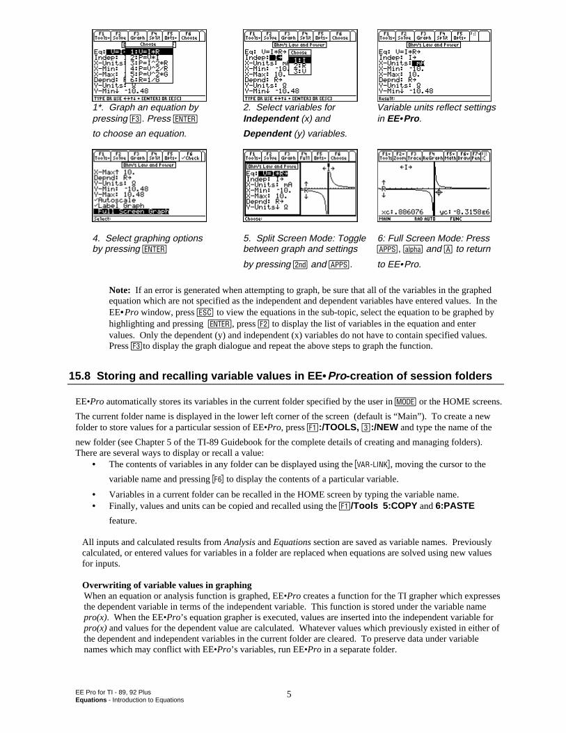
EE Pro for TI - 89, 92 PlusEquations - Introduction to Equations
5
1*. Graph an equation by 2. Select variables for Variable units reflect settings pressing …. Press ¸ Independent (x) and in EE•Pro .
to choose an equation. Dependent (y) variables.
4. Select graphing options 5. Split Screen Mode: Toggle 6: Full Screen Mode: Press by pressing ¸ between graph and settings O, j and Ñ to return
by pressing 2 and O. to EE•Pro.
Note: If an error is generated when attempting to graph, be sure that all of the variables in the graphedequation which are not specified as the independent and dependent variables have entered values. In theEE•Pro window, press N to view the equations in the sub-topic, select the equation to be graphed byhighlighting and pressing , press „ to display the list of variables in the equation and entervalues. Only the dependent (y) and independent (x) variables do not have to contain specified values.Press …to display the graph dialogue and repeat the above steps to graph the function.
15.8 Storing and recalling variable values in EE •Pro-creation of session folders
EE•Pro automatically stores its variables in the current folder specified by the user in 3 or the HOME screens.
The current folder name is displayed in the lower left corner of the screen (default is “Main”). To create a newfolder to store values for a particular session of EE•Pro, press ƒ:/TOOLS, ª:/NEW and type the name of the
new folder (see Chapter 5 of the TI-89 Guidebook for the complete details of creating and managing folders). There are several ways to display or recall a value:
• The contents of variables in any folder can be displayed using the °, moving the cursor to the
variable name and pressing to display the contents of a particular variable.
• Variables in a current folder can be recalled in the HOME screen by typing the variable name.• Finally, values and units can be copied and recalled using the ƒ/Tools 5:COPY and 6:PASTE
feature.
All inputs and calculated results from Analysis and Equations section are saved as variable names. Previouslycalculated, or entered values for variables in a folder are replaced when equations are solved using new valuesfor inputs.
Overwriting of variable values in graphingWhen an equation or analysis function is graphed, EE•Pro creates a function for the TI grapher which expressesthe dependent variable in terms of the independent variable. This function is stored under the variable namepro(x). When the EE•Pro’s equation grapher is executed, values are inserted into the independent variable forpro(x) and values for the dependent value are calculated. Whatever values which previously existed in either ofthe dependent and independent variables in the current folder are cleared. To preserve data under variablenames which may conflict with EE•Pro’s variables, run EE•Pro in a separate folder.
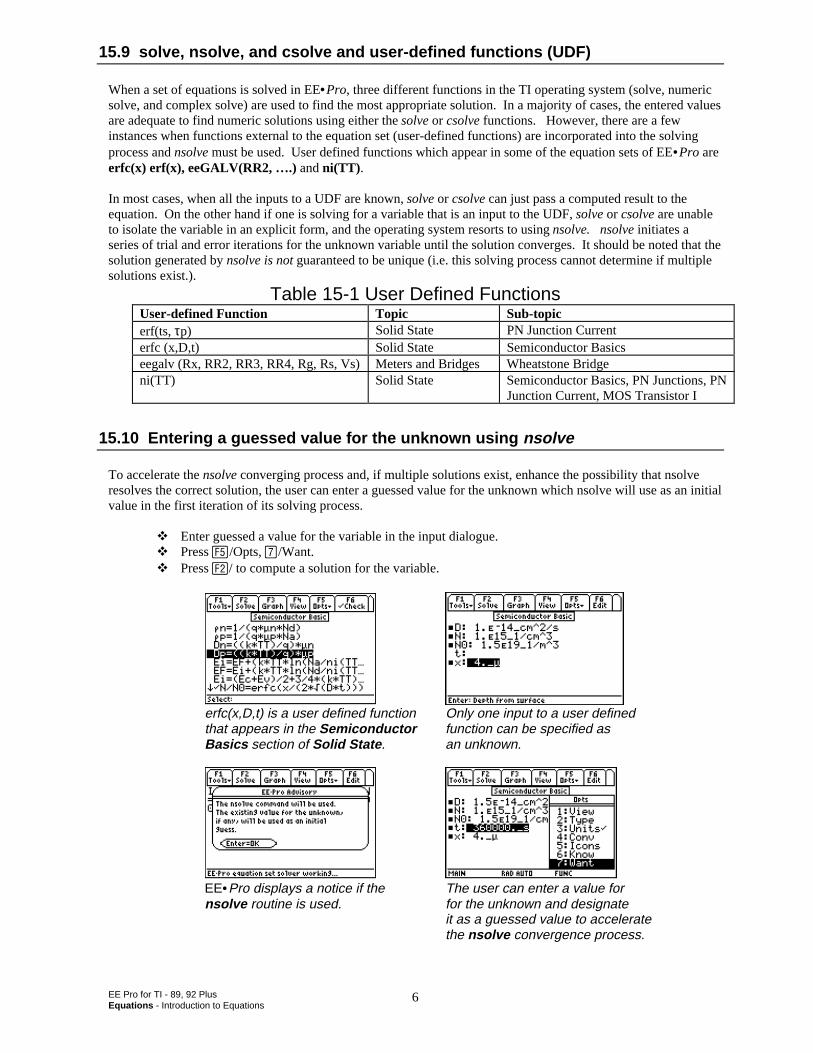
EE Pro for TI - 89, 92 PlusEquations - Introduction to Equations
6
15.9 solve, nsolve, and csolve and user-defined functions (UDF)
When a set of equations is solved in EE•Pro, three different functions in the TI operating system (solve, numericsolve, and complex solve) are used to find the most appropriate solution. In a majority of cases, the entered valuesare adequate to find numeric solutions using either the solve or csolve functions. However, there are a fewinstances when functions external to the equation set (user-defined functions) are incorporated into the solvingprocess and nsolve must be used. User defined functions which appear in some of the equation sets of EE•Pro areerfc(x) erf(x), eeGALV(RR2, ….) and ni(TT) . In most cases, when all the inputs to a UDF are known, solve or csolve can just pass a computed result to theequation. On the other hand if one is solving for a variable that is an input to the UDF, solve or csolve are unableto isolate the variable in an explicit form, and the operating system resorts to using nsolve. nsolve initiates aseries of trial and error iterations for the unknown variable until the solution converges. It should be noted that thesolution generated by nsolve is not guaranteed to be unique (i.e. this solving process cannot determine if multiplesolutions exist.).
Table 15-1 User Defined Functions User-defined Function Topic Sub-topic erf(ts, τp) Solid State PN Junction Current erfc (x,D,t) Solid State Semiconductor Basics eegalv (Rx, RR2, RR3, RR4, Rg, Rs, Vs) Meters and Bridges Wheatstone Bridge ni(TT) Solid State Semiconductor Basics, PN Junctions, PN
Junction Current, MOS Transistor I
15.10 Entering a guessed value for the unknown using nsolve
To accelerate the nsolve converging process and, if multiple solutions exist, enhance the possibility that nsolveresolves the correct solution, the user can enter a guessed value for the unknown which nsolve will use as an initialvalue in the first iteration of its solving process.
Enter guessed a value for the variable in the input dialogue.Press ‡/Opts, m/Want.Press „/ to compute a solution for the variable.
erfc(x,D,t) is a user defined function Only one input to a user definedthat appears in the Semiconductor function can be specified asBasics section of Solid State . an unknown.
EE•Pro displays a notice if the The user can enter a value fornsolve routine is used. for the unknown and designate
it as a guessed value to acceleratethe nsolve convergence process.
EE Pro for TI - 89, 92 PlusEquations - Introduction to Equations
7
15.11 Why can't I compute a solution?
If a solution is unable to be computed for an entered problem, you might check the following:
1. Are there at least as many equations selected as there are unknown parameters?2. Are the entered values or units for the known parameters reasonable for a specific case?3. Are the selected equations consistent in describing a particular case (for example, the choice of certain
equations used in the calculation of diode properties depends on whether the donor density of the dopingsubstance Nd, exceeds the acceptor density, Na in the Semiconductors section of Solid State)
15.12 Care in choosing a consistent set of equations
The success of the equation solver in generating a useful solution, or a solution at all, is strongly dependent on theuser's insight into the problem and care in choosing equations which describe consistent relationships between theparameters.
The following steps are suggested:• Read the description of each set of equations in a topic to determine which subset of equations in a series are
compatible and consistent in describing a particular case.• Select the equations from a subset which describe the relationships between all of the known and unknown
parameters.• As a rule of thumb, select as many equations from the subset as there are unknowns to avoid redundancy or
over-specification. The equations have been researched from a variety of sources and use slightly differentapproximation techniques. Over-specification (selecting too many equations) may lead to an inability of theequation solver to resolve slight numerical differences in different empirical methods of calculating values forthe same variable.
15.13 Notes for the advanced user in troubleshooting calculations
When there are no solutions possible, EE•Pro provides important clues via key variables eeinput, eeprob, eeans,and eeanstyp. These variables are defined during the equation setup process by the built-in multiple equationsolver. EE•Pro saves a copy of the problem, its inputs, its outputs, and a characterization of the type of solution inthe user variables eeprob, eeinput, eeans, and eeanstyp. For the developer who is curious to know exactly howthe problem was entered into the multiple equation solver, or about what the multiple equation solver returned, andto examine relevant strings. The contents of these variables may be viewed by using VAR-LINK and examiningthese variables in the current session. Press ° (2 followed by |), scroll to the variable name in the
current folder and press to view the contents of the variable. The string may be recalled to the author line of
the home screen, modified and re-executed, if desired.
Table 15.2 Topics and Sub-topics List1: Resistive Circuits
1: Resistance Formulas2: Ohm's Law and Power3: Temperature Effect4: Max. Power Transfer5: V, I Source
2: Capacitors, E-Fields1: Point Charge2: Long Charged Line3: Charged Disk4: Parallel Plates5: Parallel Wires6: Coaxial Cable7: Sphere
3: Inductors and Magnetism1: Long Line2: Long Strip3: Parallel Wires4: Loop5: Coaxial Cable6: Skin Effect
4: Electron Motion1: Beam Deflection2: Thermionic Emission3: Photoemission
5: Meters and Bridge Circuits1: A, V, Ω Meters2: Wheatstone Bridge3: Wien Bridge4: Maxwell Bridge5: Attenuators - Symmetric R6: Attenuators - Unsym R
6: RL and RC Circuits1: RL Natural Response2: RC Natural Response3: RL Step response4: RC Step Response5: RL Series to Parallel6: RC Series to Parallel
7: RLC Circuits1: Series Impedance
8: AC Circuits1: RL Series Impedance
9: Polyphase Circuits1: Balanced ∆ Network

EE Pro for TI - 89, 92 PlusEquations - Introduction to Equations
8
2: Parallel Admittance3: RLC Natural Response4: Under-damped case5: Critical Damping6: Over-damped Case
2: RC Series Impedance3: Impedance - Admittance4: 2 Z's in Series5: 2 Z's in Parallel
2: Balance Wye Network3: Power Measurements
10: Electrical Resonance1: Parallel Resonance I2: Parallel Resonance II3: Lossy Inductor4: Series Resonance
11: Op. Amp Circuits1: Basic Inverter2: Non-Inverting Amplifier3: Current Amplifier4: Transconductance Amplifier5: Lvl. Detector Invert6: Lvl. Detector Non-Invert7: Differentiator8: Diff. Amplifier
12: Solid State Devices1: Semiconductor Basics2: PN Junctions3: PN Junction Currents4: Transistor Currents5: Ebers-Moll Equations6: Ideal Currents - pnp7: Switching Transients8: MOS Transistor I9: MOS Transistor IIA: MOS Inverter R LoadB: MOS Inverter Sat LoadC: MOS Inverter Depl. LdD: CMOS Transistor PairE: Junction FET
13: Linear Amplifiers1: BJT (CB)2: BJT (CE)3: BJT (CC)4: FET (Common Gate)5: FET (Common Source)6: FET (Common Drain)7: Darlington (CC-CC)8: Darlington (CC-CE)9: EC AmplifierA: Differential AmplifierB: Source Coupled JFET
14: Class A, B, C Amps1: Class A Amplifier2: Power Transistor3: Push-Pull Principle4: Class B Amplifier5: Class C Amplifier
15: Transformers1. Ideal Transformer2: Linear Equiv. Circuit
16: Motors, Generators1: Energy Conversion2: DC Generator3: Sep. Excited DC Gen.4: DC Shunt Generator5: DC Series Generator6: Sep Excite DC Motor7: DC Shunt Motor8: DC Series Motor9: Perm Magnet MotorA: Induction Motor IB: Induction Motor IIC: 1 φ Induction MotorD: Synchronous Machines
EE Pro for TI - 89, 92 PlusEquations - Resistive Circuits
9
Chapter 16 Resistive CircuitsThis software section performs routine calculations of resistive circuits. The software is organized in a number oftopics listed below.
Resistance and ConductanceOhm’s Law and PowerTemperature Effects
Maximum Power TheoremV and I Source Equivalence
Variables
A complete list of all the variables used, a brief description and applicable base unit is given below.
Variable Description Unit
A Area m2
G Conductance SI Current AIl Load current AIs Current source Alen Length mP Power WPmax Maximum power in load WR Resistance ΩRl Load resistance ΩRlm Match load resistance ΩRR1 Resistance, T1 ΩRR2 Resistance, T2 ΩRs Source resistance ΩT1 Temperature 1 KT2 Temperature 2 KV Voltage VVl Load voltage VVs Source voltage Vα Temperature coefficient 1/°Kρ Resistivity Ω*mσ Conductivity S/m
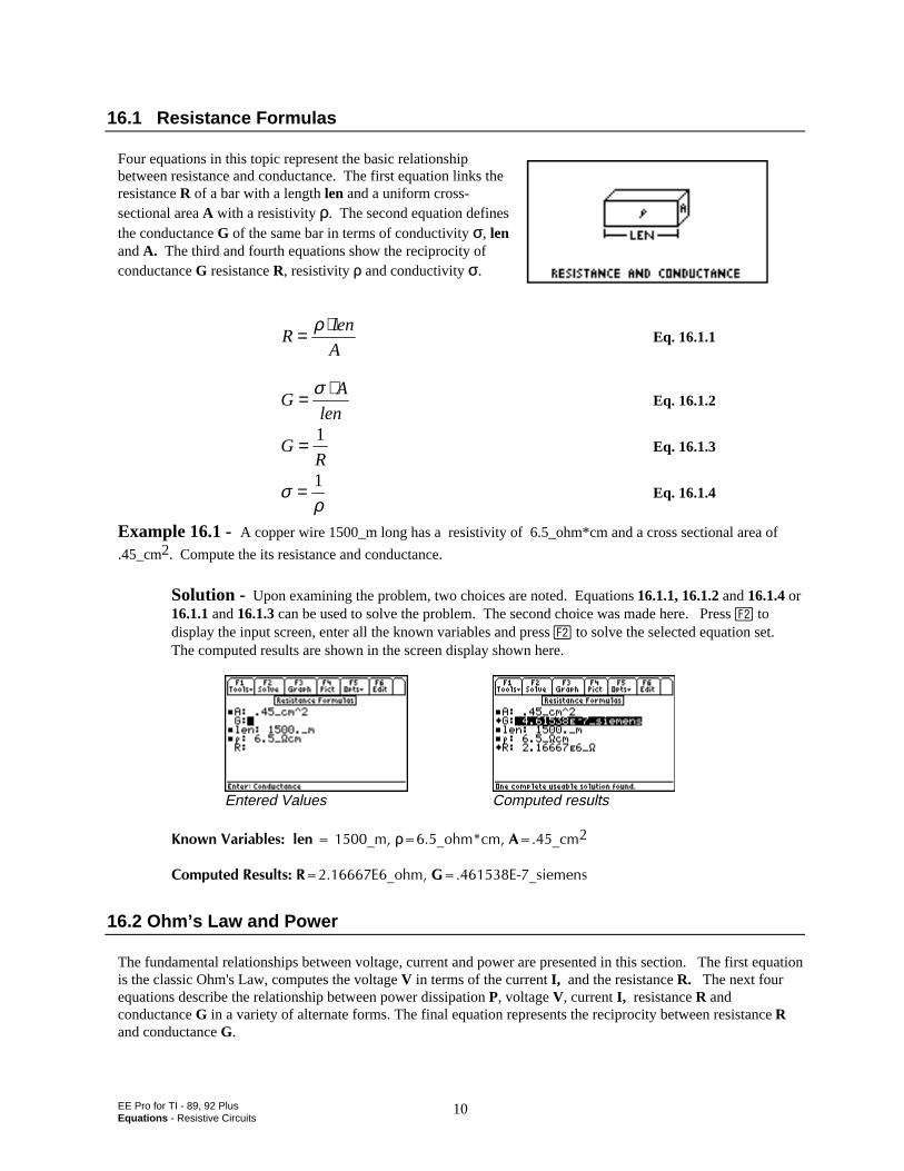
EE Pro for TI - 89, 92 PlusEquations - Resistive Circuits
10
16.1 Resistance Formulas
Four equations in this topic represent the basic relationshipbetween resistance and conductance. The first equation links theresistance R of a bar with a length len and a uniform cross-sectional area A with a resistivity ρ. The second equation definesthe conductance G of the same bar in terms of conductivity σ, lenand A. The third and fourth equations show the reciprocity ofconductance G resistance R, resistivity ρ and conductivity σ.
Rlen
A= ⋅ρ
Eq. 16.1.1
GA
len= ⋅σ
Eq. 16.1.2
GR
= 1Eq. 16.1.3
σρ
= 1Eq. 16.1.4
Example 16.1 - A copper wire 1500_m long has a resistivity of 6.5_ohm*cm and a cross sectional area of
.45_cm2. Compute the its resistance and conductance.
Solution - Upon examining the problem, two choices are noted. Equations 16.1.1, 16.1.2 and 16.1.4 or16.1.1 and 16.1.3 can be used to solve the problem. The second choice was made here. Press „ todisplay the input screen, enter all the known variables and press „ to solve the selected equation set.The computed results are shown in the screen display shown here.
Entered Values Computed results
-PQYP8CTKCDNGUNGPAOρAQJOEO#AEO
%QORWVGF4GUWNVU4'AQJO)'AUKGOGPU
16.2 Ohm’s Law and Power
The fundamental relationships between voltage, current and power are presented in this section. The first equationis the classic Ohm's Law, computes the voltage V in terms of the current I, and the resistance R. The next fourequations describe the relationship between power dissipation P, voltage V, current I, resistance R andconductance G in a variety of alternate forms. The final equation represents the reciprocity between resistance Rand conductance G.
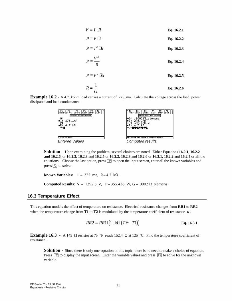
EE Pro for TI - 89, 92 PlusEquations - Resistive Circuits
11
V I R= ⋅ Eq. 16.2.1
P V I= ⋅ Eq. 16.2.2
P I R= ⋅2 Eq. 16.2.3
PV
R=
2
Eq. 16.2.4
P V G= ⋅2 Eq. 16.2.5
RG
= 1Eq. 16.2.6
Example 16.2 - A 4.7_kohm load carries a current of 275_ma. Calculate the voltage across the load, powerdissipated and load conductance.
Entered Values Computed results
Solution - Upon examining the problem, several choices are noted. Either Equations 16.2.1, 16.2.2and 16.2.6, or 16.2.2, 16.2.3 and 16.2.5 or 16.2.2, 16.2.3 and 16.2.6 or 16.2.1, 16.2.2 and 16.2.5 or all theequations. Choose the last option, press „ to open the input screen, enter all the known variables andpress „ to solve.
-PQYP8CTKCDNGU+AOC4AMΩ
%QORWVGF4GUWNVU8A82A9)AUKGOGPU
16.3 Temperature Effect
This equation models the effect of temperature on resistance. Electrical resistance changes from RR1 to RR2when the temperature change from T1 to T2 is modulated by the temperature coefficient of resistance α.
RR RR T T2 1 1 2 1= ⋅ + ⋅ −α b gc h Eq. 16.3.1
Example 16.3 - A 145_Ω resistor at 75_°F reads 152.4_Ω at 125_ºC. Find the temperature coefficient ofresistance.
Solution - Since there is only one equation in this topic, there is no need to make a choice of equation.Press „ to display the input screen. Enter the variable values and press „ to solve for the unknownvariable.
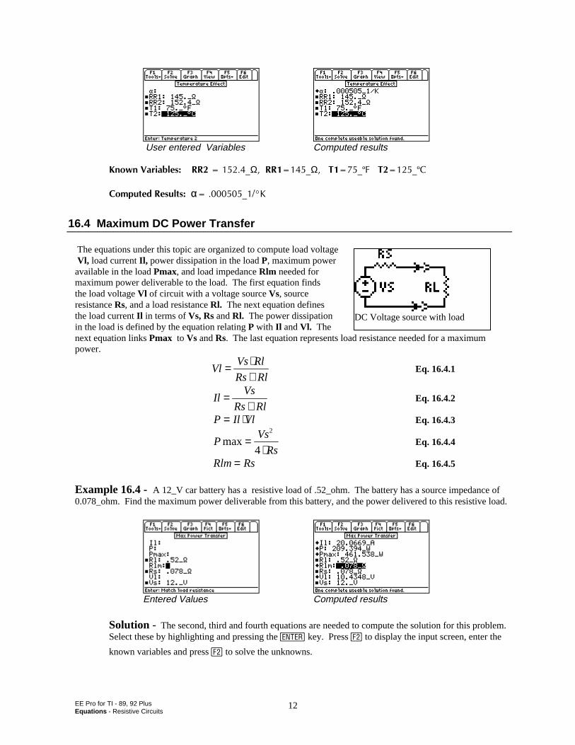
EE Pro for TI - 89, 92 PlusEquations - Resistive Circuits
12
User entered Variables Computed results
-PQYP8CTKCDNGU44AΩ44AΩ6Aº(6Aº%
%QORWVGF4GUWNVUαAu-
16.4 Maximum DC Power Transfer
The equations under this topic are organized to compute load voltage Vl, load current Il, power dissipation in the load P, maximum poweravailable in the load Pmax, and load impedance Rlm needed formaximum power deliverable to the load. The first equation findsthe load voltage Vl of circuit with a voltage source Vs, sourceresistance Rs, and a load resistance Rl. The next equation definesthe load current Il in terms of Vs, Rs and Rl. The power dissipationin the load is defined by the equation relating P with Il and Vl. Thenext equation links Pmax to Vs and Rs. The last equation represents load resistance needed for a maximumpower.
VlVs Rl
Rs Rl= ⋅
+Eq. 16.4.1
IlVs
Rs Rl=
+Eq. 16.4.2
P Il Vl= ⋅ Eq. 16.4.3
PVs
Rsmax=
⋅
2
4Eq. 16.4.4
Rlm Rs= Eq. 16.4.5
Example 16.4 - A 12_V car battery has a resistive load of .52_ohm. The battery has a source impedance of0.078_ohm. Find the maximum power deliverable from this battery, and the power delivered to this resistive load.
Entered Values Computed results
Solution - The second, third and fourth equations are needed to compute the solution for this problem.Select these by highlighting and pressing the key. Press „ to display the input screen, enter the
known variables and press „ to solve the unknowns.
DC Voltage source with load
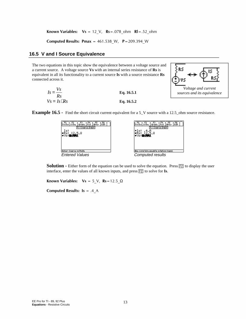
EE Pro for TI - 89, 92 PlusEquations - Resistive Circuits
13
-PQYP8CTKCDNGU8UA84UAQJO4NAQJO
%QORWVGF4GUWNVU2OCZA92A9
16.5 V and I Source Equivalence
The two equations in this topic show the equivalence between a voltage source anda current source. A voltage source Vs with an internal series resistance of Rs isequivalent in all its functionality to a current source Is with a source resistance Rsconnected across it.
IsVs
Rs= Eq. 16.5.1
Vs Is Rs= ⋅ Eq. 16.5.2
Example 16.5 - Find the short circuit current equivalent for a 5_V source with a 12.5_ohm source resistance.
Entered Values Computed results
Solution - Either form of the equation can be used to solve the equation. Press „ to display the userinterface, enter the values of all known inputs, and press „ to solve for Is.
-PQYP8CTKCDNGU8UA84UAΩ
%QORWVGF4GUWNVU+UA#
Voltage and currentsources and its equivalence

EE Pro for TI - 89, 92 PlusEquations - Capacitors & Electric Fields
14
Chapter 17 Capacitors, Electric Fields
This section covers seven topics to compute electric field propertiesand capacitance of various types of structures.
When the section is accessed, the software displays the topics in apop up menu shown above.
Point ChargeLong Charged LineCharged DiskParallel PlatesParallel Wires
Coaxial CableSphere
Variables
A complete list of all the variables used in this section is given below.
Variable Description Unit
A Area m2
C Capacitance Fcl Capacitance per unit length F/md Separation mE Electric field V/mEr Radial electric field V/mEz Electric field along z axis V/mF Force on plate NQ Charge Cr Radial distance mra Inner radius, wire radius mrb Outer radius mV Potential VVz Potential along z axis VW Energy stored Jz z axis distance from disk mεr Relative permittivity unitlessρl Line charge C/m
ρs Charge density C/m2
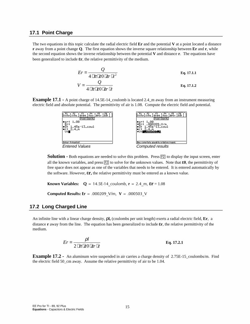
EE Pro for TI - 89, 92 PlusEquations - Capacitors & Electric Fields
15
17.1 Point Charge
The two equations in this topic calculate the radial electric field Er and the potential V at a point located a distancer away from a point change Q. The first equation shows the inverse square relationship between Er and r, whilethe second equation shows the inverse relationship between the potential V and distance r . The equations havebeen generalized to include εr , the relative permittivity of the medium.
ErQ
r r=
⋅ ⋅ ⋅ ⋅4 0 2π ε εEq. 17.1.1
VQ
r r=
⋅ ⋅ ⋅ ⋅4 0π ε εEq. 17.1.2
Example 17.1 - A point charge of 14.5E-14_coulomb is located 2.4_m away from an instrument measuringelectric field and absolute potential. The permittivity of air is 1.08. Compute the electric field and potential.
Entered Values Computed results
Solution - Both equations are needed to solve this problem. Press „ to display the input screen, enter
all the known variables, and press „ to solve for the unknown values. Note that ε0, the permittivity offree space does not appear as one of the variables that needs to be entered. It is entered automatically bythe software. However, εr , the relative permittivity must be entered as a known value.
-PQYP8CTKCDNGU3'AEQWNQODTAOεr = 1.08
%QORWVGF4GUWNVU'TA8O8A8
17.2 Long Charged Line
An infinite line with a linear charge density, ρl, (coulombs per unit length) exerts a radial electric field, Er , adistance r away from the line. The equation has been generalized to include εr , the relative permittivity of themedium.
Erl
r r=
⋅ ⋅ ⋅ ⋅ρ
π ε ε2 0Eq. 17.2.1
Example 17.2 - An aluminum wire suspended in air carries a charge density of 2.75E-15_coulombs/m. Findthe electric field 50_cm away. Assume the relative permittivity of air to be 1.04.
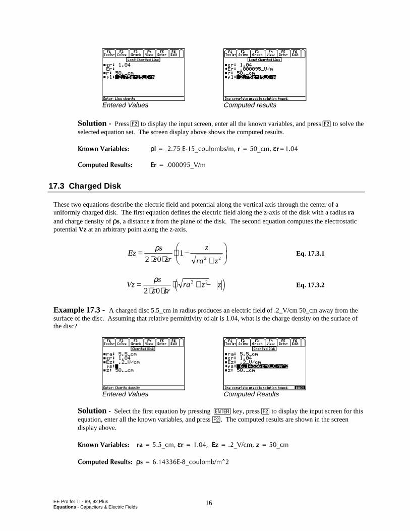
EE Pro for TI - 89, 92 PlusEquations - Capacitors & Electric Fields
16
Entered Values Computed results
Solution - Press „ to display the input screen, enter all the known variables, and press „ to solve theselected equation set. The screen display above shows the computed results.
-PQYP8CTKCDNGU ρN'AEQWNQODUOTAEOεT
%QORWVGF4GUWNVU 'TA8O
17.3 Charged Disk
These two equations describe the electric field and potential along the vertical axis through the center of auniformly charged disk. The first equation defines the electric field along the z-axis of the disk with a radius raand charge density of ρs, a distance z from the plane of the disk. The second equation computes the electrostaticpotential Vz at an arbitrary point along the z-axis.
Ezs
r
z
ra z=
⋅ ⋅⋅ −
+
FHG
IKJ
ρε ε2 0
12 2
Eq. 17.3.1
Vzs
rra z z=
⋅ ⋅⋅ + −ρ
ε ε2 02 2e j Eq. 17.3.2
Example 17.3 - A charged disc 5.5_cm in radius produces an electric field of .2_V/cm 50_cm away from thesurface of the disc. Assuming that relative permittivity of air is 1.04, what is the charge density on the surface ofthe disc?
Entered Values Computed Results
Solution - Select the first equation by pressing key, press „ to display the input screen for thisequation, enter all the known variables, and press „. The computed results are shown in the screendisplay above.
-PQYP8CTKCDNGUTCAEOεT'\A8EO\AEO
%QORWVGF4GUWNVUρU'AEQWNQODO@
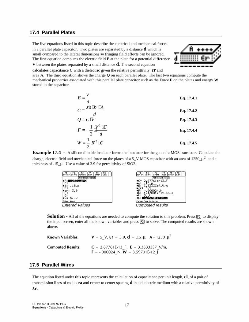
EE Pro for TI - 89, 92 PlusEquations - Capacitors & Electric Fields
17
17.4 Parallel Plates
The five equations listed in this topic describe the electrical and mechanical forcesin a parallel plate capacitor. Two plates are separated by a distance d which issmall compared to the lateral dimensions so fringing field effects can be ignored.The first equation computes the electric field E at the plate for a potential differenceV between the plates separated by a small distance d. The second equation
calculates capacitance C with a dielectric given the relative permittivity εr andarea A. The third equation shows the charge Q on each parallel plate. The last two equations compute themechanical properties associated with this parallel plate capacitor such as the Force F on the plates and energy Wstored in the capacitor.
EV
d= Eq. 17.4.1
Cr A
d= ⋅ ⋅ε ε0
Eq. 17.4.2
Q C V= ⋅ Eq. 17.4.3
FV C
d= − ⋅ ⋅1
2
2
Eq. 17.4.4
W V C= ⋅ ⋅1
22 Eq. 17.4.5
Example 17.4 - A silicon dioxide insulator forms the insulator for the gate of a MOS transistor. Calculate the
charge, electric field and mechanical force on the plates of a 5_V MOS capacitor with an area of 1250_µ2 and athickness of .15_µ. Use a value of 3.9 for permittivity of SiO2.
Entered Values Computed results
Solution - All of the equations are needed to compute the solution to this problem. Press „ to displaythe input screen, enter all the known variables and press „ to solve. The computed results are shownabove.
-PQYP8CTKCDNGU 8A8εTF.15_µ. #_µ2
%QORWVGF4GUWNVU %'A(''A8O(A09'A,
17.5 Parallel Wires
The equation listed under this topic represents the calculation of capacitance per unit length, cl, of a pair of
transmission lines of radius ra and center to center spacing d in a dielectric medium with a relative permittivity of
εr .
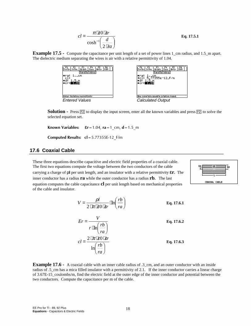
EE Pro for TI - 89, 92 PlusEquations - Capacitors & Electric Fields
18
clr
d
ra
= ⋅ ⋅
⋅FHG
IKJ
−
π ε ε0
21cosh
Eq. 17.5.1
Example 17.5 - Compute the capacitance per unit length of a set of power lines 1_cm radius, and 1.5_m apart.The dielectric medium separating the wires is air with a relative permittivity of 1.04.
Entered Values Calculated Output
Solution - Press „ to display the input screen, enter all the known variables and press „ to solve theselected equation set.
-PQYP8CTKCDNGUεTTCAEOFAO
%QORWVGF4GUWNVUEN'A(O
17.6 Coaxial Cable
These three equations describe capacitive and electric field properties of a coaxial cable.The first two equations compute the voltage between the two conductors of the cable
carrying a charge of ρl per unit length, and an insulator with a relative permittivity εr . The
inner conductor has a radius ra while the outer conductor has a radius rb . The last
equation computes the cable capacitance cl per unit length based on mechanical propertiesof the cable and insulator.
Vl
r
rb
ra=
⋅ ⋅ ⋅⋅ F
HGIKJ
ρπ ε ε2 0
ln Eq. 17.6.1
ErV
rrb
ra
=⋅ F
HGIKJln
Eq. 17.6.2
clr
rb
ra
= ⋅ ⋅ ⋅FHG
IKJ
2 0π ε ε
lnEq. 17.6.3
Example 17.6 - A coaxial cable with an inner cable radius of .3_cm, and an outer conductor with an insideradius of .5_cm has a mica filled insulator with a permittivity of 2.1. If the inner conductor carries a linear chargeof 3.67E-15_coulombs/m, find the electric field at the outer edge of the inner conductor and potential between thetwo conductors. Compute the capacitance per m of the cable.
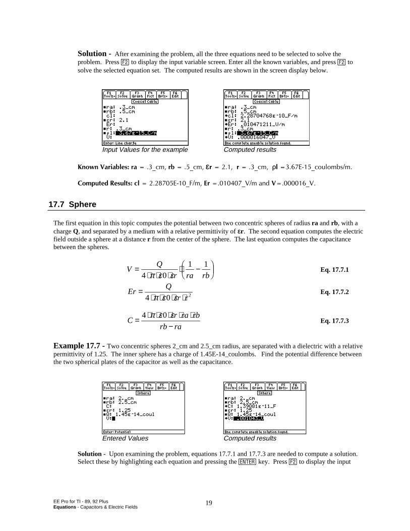
EE Pro for TI - 89, 92 PlusEquations - Capacitors & Electric Fields
19
Solution - After examining the problem, all the three equations need to be selected to solve theproblem. Press „ to display the input variable screen. Enter all the known variables, and press „ tosolve the selected equation set. The computed results are shown in the screen display below.
Input Values for the example Computed results
-PQYP8CTKCDNGUTCAEOTDAEOεTTAEOρN'AEQWNQODUO
%QORWVGF4GUWNVUEN'A(O'TA8OCPF8A8
17.7 Sphere
The first equation in this topic computes the potential between two concentric spheres of radius ra and rb , with acharge Q, and separated by a medium with a relative permittivity of εr . The second equation computes the electricfield outside a sphere at a distance r from the center of the sphere. The last equation computes the capacitancebetween the spheres.
VQ
r ra rb=
⋅ ⋅ ⋅⋅ −FHG
IKJ4 0
1 1
π ε εEq. 17.7.1
ErQ
r r=
⋅ ⋅ ⋅ ⋅4 0 2π ε εEq. 17.7.2
Cr ra rb
rb ra= ⋅ ⋅ ⋅ ⋅ ⋅
−4 0π ε ε
Eq. 17.7.3
Example 17.7 - Two concentric spheres 2_cm and 2.5_cm radius, are separated with a dielectric with a relativepermittivity of 1.25. The inner sphere has a charge of 1.45E-14_coulombs. Find the potential difference betweenthe two spherical plates of the capacitor as well as the capacitance.
Entered Values Computed results
Solution - Upon examining the problem, equations 17.7.1 and 17.7.3 are needed to compute a solution.Select these by highlighting each equation and pressing the key. Press „ to display the input

EE Pro for TI - 89, 92 PlusEquations - Capacitors & Electric Fields
20
screen. Enter all the known variables, and press „ to solve the selected equation set. The computedresults are shown in the screen display shown here.
-PQYP8CTKCDNGUTCAEOTDAEOεTCPF3'AEQWNQODU
%QORWVGF4GUWNVU8A8%'A(
EE PRO for TI - 89, 92 PlusEquations - Inductance & Magnetism
21
Chapter 18 Inductors and MagnetismTopics in this section focus on electrical and magnetic properties of physical elements.
Long LineLong StripParallel Wires
LoopCoaxial CableSkin Effect
Variables
A complete list of all the variables used in the various topics of this section are listed below along with thedefault units used for those variables.
Variable Description Unitθ Angle radianµr Relative permeability unitlessa Loop radius or side of a rectangular loop mB Magnetic field Tbl Width of rectangular loop mBx Magnetic field, x axis TBy Magnetic field, y axis TD Center-center wire spacing md Strip width mf Frequency HzFw Force between wires/unit length N/mI Current AI1 Current in line 1 AI2 Current in line 2 AIs Current in strip A/mL Inductance per unit length H/mL12 Mutual inductance HLs Loop self-inductance Hr Radial distance mra Radius of inner conductor mrb Radius of outer conductor mReff Effective resistance Ωrr0 Wire radius mT12 Torque N*mx x axis distance my y axis distance mz Distance to loop z axis m
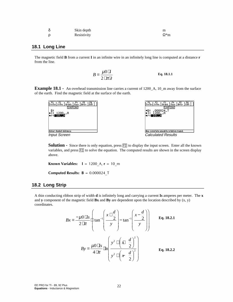
EE PRO for TI - 89, 92 PlusEquations - Inductance & Magnetism
22
δ Skin depth mρ Resistivity Ω*m
18.1 Long Line
The magnetic field B from a current I in an infinite wire in an infinitely long line is computed at a distance rfrom the line.
Eq. 18.1.1
Example 18.1 - An overhead transmission line carries a current of 1200_A, 10_m away from the surfaceof the earth. Find the magnetic field at the surface of the earth.
Input Screen Calculated Results
Solution - Since there is only equation, press „ to display the input screen. Enter all the knownvariables, and press „ to solve the equation. The computed results are shown in the screen displayabove.
-PQYP8CTKCDNGU+A#TAO
%QORWVGF4GUWNVU$A6
18.2 Long Strip
A thin conducting ribbon strip of width d is infinitely long and carrying a current Is amperes per meter. The xand y component of the magnetic field Bx and By are dependent upon the location described by (x, y)coordinates.
Eq. 18.2.1
Eq. 18.2.2
BxIs x
d
y
xd
y= − ⋅
⋅⋅
+F
HGGG
I
KJJJ
−−F
HGGG
I
KJJJ
F
H
GGG
I
K
JJJ
− −µπ
0
22 21 1tan tan
ByIs
y xd
y xd
= ⋅⋅
⋅+ +FHG
IKJ
+ −FHG
IKJ
F
H
GGGG
I
K
JJJJ
µπ
0
42
2
22
22ln
BI
r= ⋅
⋅ ⋅µ
π0
2
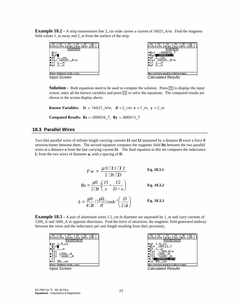
EE PRO for TI - 89, 92 PlusEquations - Inductance & Magnetism
23
Example 18.2 - A strip transmission line 2_cm wide carries a current of 16025_A/m. Find the magneticfield values 1_m away and 2_m from the surface of the strip.
Input Screen Calculated Results
Solution - Both equations need to be used to compute the solution. Press „ to display the inputscreen, enter all the known variables and press „ to solve the equations. The computed results areshown in the screen display above.
-PQYP8CTKCDNGU+UA#OFAEOZAO[AO
%QORWVGF4GUWNVU$ZA6$[A6
18.3 Parallel Wires
Two thin parallel wires of infinite length carrying currents I1 and I2 separated by a distance D exert a force Fnewtons/meter between them. The second equation computes the magnetic field Bx between the two parallelwires at a distance x from the line carrying current I1. The final equation in this set computes the inductanceL from the two wires of diameter a, with a spacing of D.
Eq. 18.3.1
Eq. 18.3.2
Eq. 18.3.3
Example 18.3 - A pair of aluminum wires 1.5_cm in diameter are separated by 1_m and carry currents of1200_A and 1600_A in opposite directions. Find the force of attraction, the magnetic field generated midwaybetween the wires and the inductance per unit length resulting from their proximity.
Input Screen Calculated Results
F wI I
D= ⋅ ⋅
⋅ ⋅µ
π0 1 2
2
BxI
x
I
D x=
⋅⋅ −
−FHG
IKJ
µπ0
2
1 2
LD
a=
⋅+ ⋅
⋅FHG
IKJ
−µπ
µπ
0
4
0
21cosh
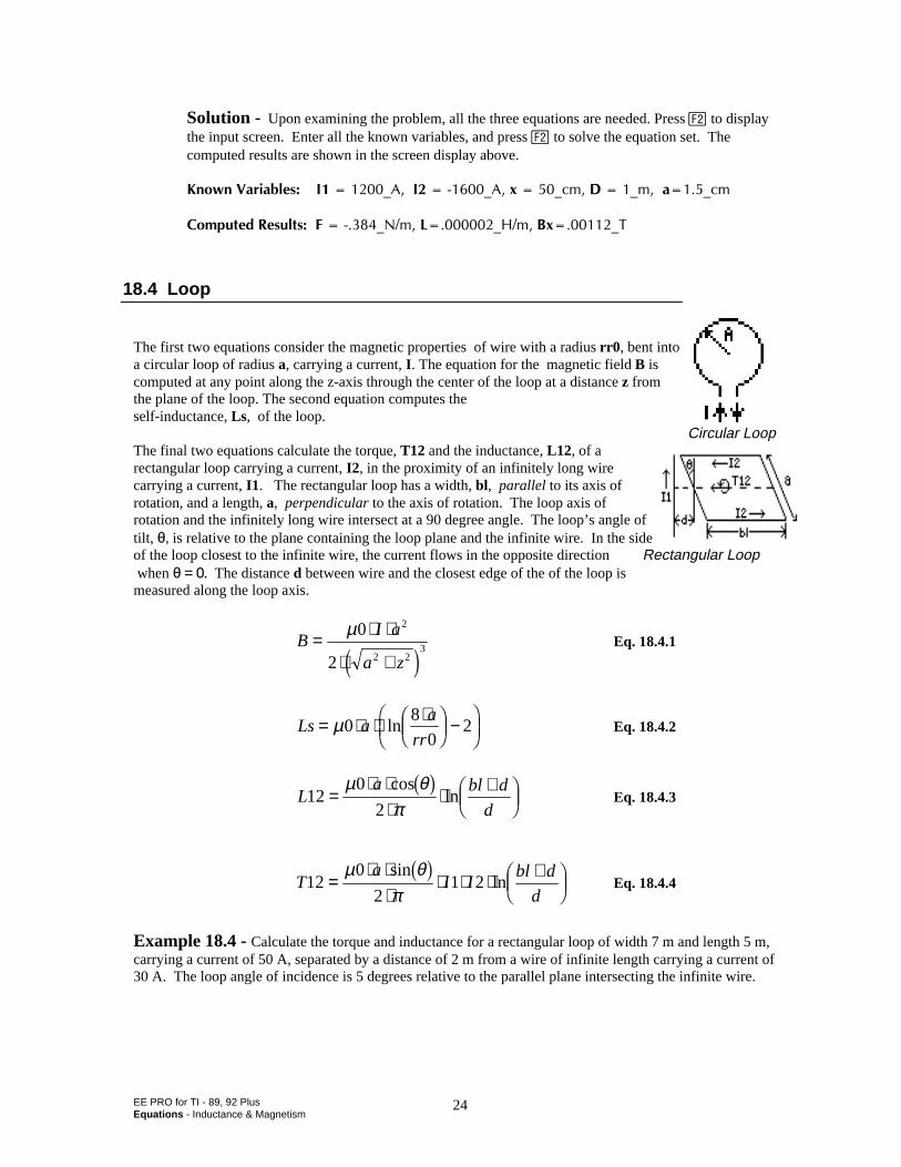
EE PRO for TI - 89, 92 PlusEquations - Inductance & Magnetism
24
Solution - Upon examining the problem, all the three equations are needed. Press „ to displaythe input screen. Enter all the known variables, and press „ to solve the equation set. Thecomputed results are shown in the screen display above.
-PQYP8CTKCDNGU+A#+A#ZAEO&AOCAEO
%QORWVGF4GUWNVU(A0O.A*O$ZA6
18.4 Loop
The first two equations consider the magnetic properties of wire with a radius rr0 , bent intoa circular loop of radius a, carrying a current, I . The equation for the magnetic field B iscomputed at any point along the z-axis through the center of the loop at a distance z fromthe plane of the loop. The second equation computes theself-inductance, Ls, of the loop.
Circular LoopThe final two equations calculate the torque, T12 and the inductance, L12, of arectangular loop carrying a current, I2, in the proximity of an infinitely long wirecarrying a current, I1. The rectangular loop has a width, bl, parallel to its axis ofrotation, and a length, a, perpendicular to the axis of rotation. The loop axis ofrotation and the infinitely long wire intersect at a 90 degree angle. The loop’s angle oftilt, θ, is relative to the plane containing the loop plane and the infinite wire. In the sideof the loop closest to the infinite wire, the current flows in the opposite direction Rectangular Loop when θ = 0. The distance d between wire and the closest edge of the of the loop ismeasured along the loop axis.
BI a
a z= ⋅ ⋅
⋅ +
µ0
2
2
2 23
e jEq. 18.4.1
Ls aa
rr= ⋅ ⋅ ⋅F
HGIKJ −F
HGIKJµ0
8
02ln Eq. 18.4.2
La bl d
d12
0
2=
⋅ ⋅⋅
⋅ +FHG
IKJ
µ θπcos
lnb g
Eq. 18.4.3
Ta
I Ibl d
d12
0
21 2=
⋅ ⋅⋅
⋅ ⋅ ⋅ +FHG
IKJ
µ θπsin
lnb g
Eq. 18.4.4
Example 18.4 - Calculate the torque and inductance for a rectangular loop of width 7 m and length 5 m,carrying a current of 50 A, separated by a distance of 2 m from a wire of infinite length carrying a current of30 A. The loop angle of incidence is 5 degrees relative to the parallel plane intersecting the infinite wire.
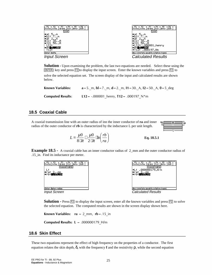
EE PRO for TI - 89, 92 PlusEquations - Inductance & Magnetism
25
Input Screen Calculated Results
SolutionUpon examining the problem, the last two equations are needed. Select these using the¸| key and press „to display the input screen. Enter the known variables and press „ to
solve the selected equation set. The screen display of the input and calculated results are shownbelow.
-PQYP8CTKCDNGU CAODNAOFAO+A#+A#θAFGI
%QORWVGF4GUWNVU .AJGPT[6A0O
18.5 Coaxial Cable
A coaxial transmission line with an outer radius of inn the inner conductor of ra and innerradius of the outer conductor of rb is characterized by the inductance L per unit length.
Lrb
ra=
⋅+
⋅⋅ F
HGIKJ
µπ
µπ
0
8
0
2ln Eq. 18.5.1
Example 18.5 - A coaxial cable has an inner conductor radius of 2_mm and the outer conductor radius of.15_in. Find its inductance per meter.
Input Screen Calculated Results
Solution - Press „ to display the input screen, enter all the known variables and press „ to solvethe selected equation. The computed results are shown in the screen display shown here.
-PQYP8CTKCDNGUTCAOOTDAKP
%QORWVGF4GUWNVU.A*O
18.6 Skin Effect
These two equations represent the effect of high frequency on the properties of a conductor. The firstequation relates the skin depth, δ, with the frequency f and the resistivity ρ, while the second equation
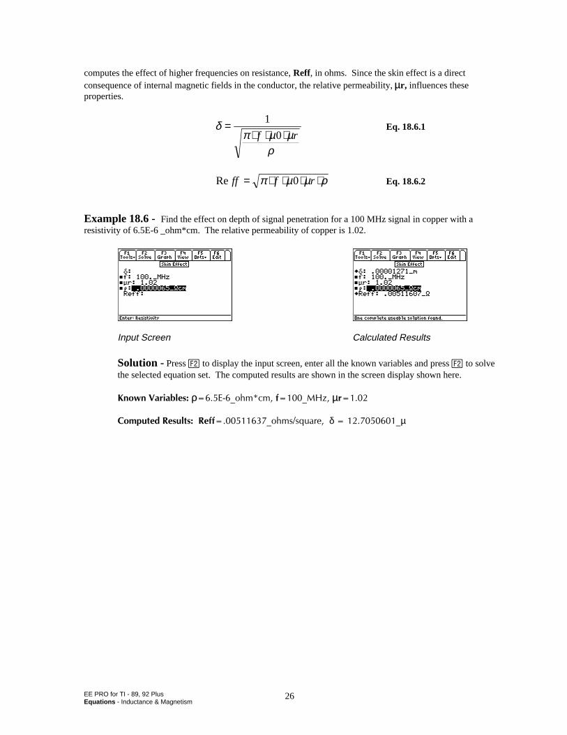
EE PRO for TI - 89, 92 PlusEquations - Inductance & Magnetism
26
computes the effect of higher frequencies on resistance, Reff, in ohms. Since the skin effect is a directconsequence of internal magnetic fields in the conductor, the relative permeability, µr, influences theseproperties.
δπ µ µ
ρ
=⋅ ⋅ ⋅
1
0f rEq. 18.6.1
Re ff f r= ⋅ ⋅ ⋅ ⋅π µ µ ρ0 Eq. 18.6.2
Example 18.6 - Find the effect on depth of signal penetration for a 100 MHz signal in copper with aresistivity of 6.5E-6 _ohm*cm. The relative permeability of copper is 1.02.
Input Screen Calculated Results
Solution - Press „ to display the input screen, enter all the known variables and press „ to solvethe selected equation set. The computed results are shown in the screen display shown here.
-PQYP8CTKCDNGUρ'AQJOEOHA/*\µT
%QORWVGF4GUWNVU4GHHAQJOUUSWCTGδAµ
EE Pro for TI-89, 92 PlusEquation s - Electron Motion
27
Chapter 19 Electron MotionThis section covers equations describing the trajectories of electrons under the influence of electric and magneticfields. These equations are divided into three topics.
Electron Beam DeflectionThermionic Emission
Photoemission
Variables
The table below lists all the variables used in this chapter.
Variable Description Unit
A0 Richardson’s constant A/(m2*K 2)B Magnetic field Td Deflection tube diameter, plate spacing mf Frequency Hzf0 Critical frequency HzI Thermionic current AL Deflecting plate length mLs Beam length to destination mr Radius of circular path m
S Surface area m2
T Temperature Kv Vertical velocity m/sVa Accelerating voltage VVd Deflecting voltage Vy Vertical deflection myd Beam deflection on screen mz Distance along beam axis mφ Work function V
19.1 Electron Beam Deflection
An electron beam that is subjected to an accelerating voltage Va achieves a velocity v as defined by the firstequation. The second equation calculates the radius of curvature r as these electrons in the beam move with avelocity v passing through a magnetic field B. The third equation calculates the y-deflection yd at distance Ls fromthe center of deflection plates separated by a distance d and length L making the approximation that the Ls>>L . Thefinal equation calculates the vertical displacement y inside the deflection region with distance z from entry into theplate region and subject to a deflecting voltage Vd.
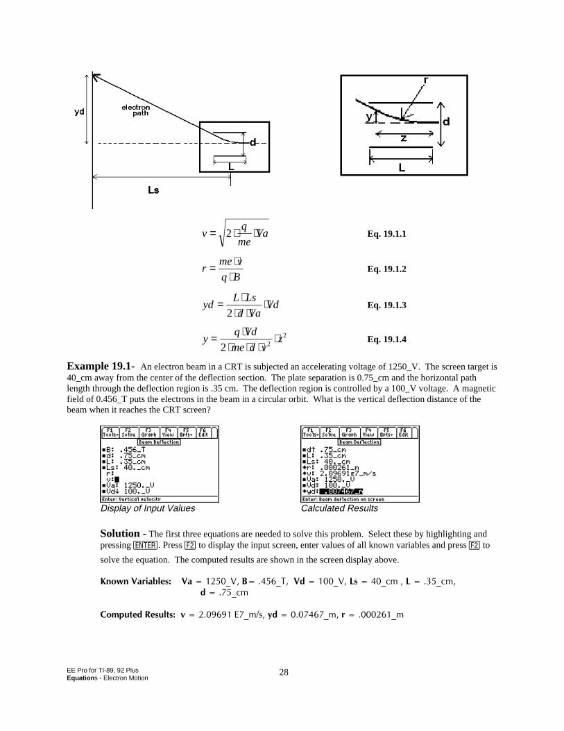
EE Pro for TI-89, 92 PlusEquation s - Electron Motion
28
vq
meVa= ⋅ ⋅2 Eq. 19.1.1
rme v
q B= ⋅
⋅Eq. 19.1.2
ydL Ls
d VaVd= ⋅
⋅ ⋅⋅
2Eq. 19.1.3
yq Vd
me d vz= ⋅
⋅ ⋅ ⋅⋅
2 22 Eq. 19.1.4
Example 19.1- An electron beam in a CRT is subjected an accelerating voltage of 1250_V. The screen target is40_cm away from the center of the deflection section. The plate separation is 0.75_cm and the horizontal pathlength through the deflection region is .35 cm. The deflection region is controlled by a 100_V voltage. A magneticfield of 0.456_T puts the electrons in the beam in a circular orbit. What is the vertical deflection distance of thebeam when it reaches the CRT screen?
Display of Input Values Calculated Results
Solution - The first three equations are needed to solve this problem. Select these by highlighting andpressing . Press „ to display the input screen, enter values of all known variables and press „ to
solve the equation. The computed results are shown in the screen display above.
-PQYP8CTKCDNGU8CA8$A68FA8.UAEO.AEOFAEO
%QORWVGF4GUWNVUX'AOU[FAOTAO
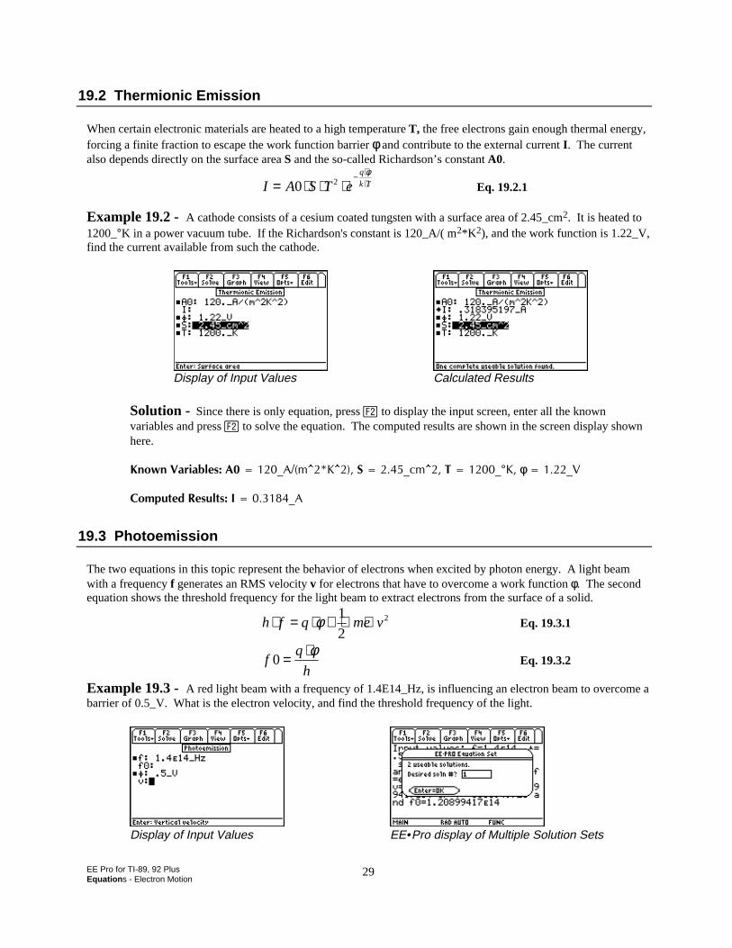
EE Pro for TI-89, 92 PlusEquation s - Electron Motion
29
19.2 Thermionic Emission
When certain electronic materials are heated to a high temperature T, the free electrons gain enough thermal energy,forcing a finite fraction to escape the work function barrier φ and contribute to the external current I . The currentalso depends directly on the surface area S and the so-called Richardson’s constant A0.
I A S T eq
k T= ⋅ ⋅ ⋅− ⋅
⋅0 2φ
Eq. 19.2.1
Example 19.2 - A cathode consists of a cesium coated tungsten with a surface area of 2.45_cm2. It is heated to1200_°K in a power vacuum tube. If the Richardson's constant is 120_A/( m2*K 2), and the work function is 1.22_V,find the current available from such the cathode.
Display of Input Values Calculated Results
Solution - Since there is only equation, press „ to display the input screen, enter all the knownvariables and press „ to solve the equation. The computed results are shown in the screen display shownhere.
-PQYP8CTKCDNGU#A#O@-@5AEO@6A°-φA8
%QORWVGF4GUWNVU+A#
19.3 Photoemission
The two equations in this topic represent the behavior of electrons when excited by photon energy. A light beamwith a frequency f generates an RMS velocity v for electrons that have to overcome a work function φ. The secondequation shows the threshold frequency for the light beam to extract electrons from the surface of a solid.
h f q me v⋅ = ⋅ + ⋅ ⋅φ 1
22 Eq. 19.3.1
fq
h0 = ⋅φ
Eq. 19.3.2
Example 19.3 - A red light beam with a frequency of 1.4E14_Hz, is influencing an electron beam to overcome abarrier of 0.5_V. What is the electron velocity, and find the threshold frequency of the light.
Display of Input Values EE•Pro display of Multiple Solution Sets
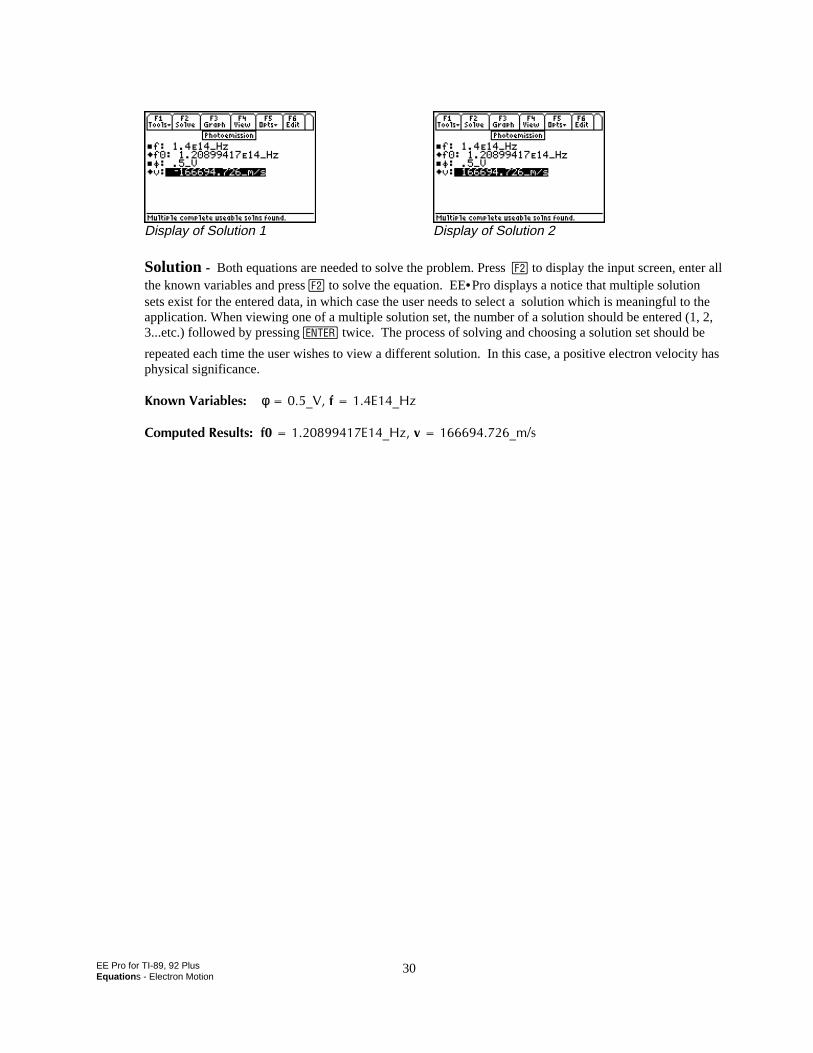
EE Pro for TI-89, 92 PlusEquation s - Electron Motion
30
Display of Solution 1 Display of Solution 2
Solution - Both equations are needed to solve the problem. Press „ to display the input screen, enter allthe known variables and press „ to solve the equation. EE•Pro displays a notice that multiple solutionsets exist for the entered data, in which case the user needs to select a solution which is meaningful to theapplication. When viewing one of a multiple solution set, the number of a solution should be entered (1, 2,3...etc.) followed by pressing twice. The process of solving and choosing a solution set should be
repeated each time the user wishes to view a different solution. In this case, a positive electron velocity hasphysical significance.
-PQYP8CTKCDNGUφA8H'A*\
%QORWVGF4GUWNVUH'A*\XAOU
EE Pro for TI-89, 92 PlusEquations - Meters and Bridge Circuits
31
Chapter 20 Meters and Bridge CircuitsThis section covers a variety of topics on meters, commonly used bridge and attenuator circuits. These equations areorganized under seven titles.
Amp, Volt, and OhmmeterWheatstone BridgeWien BridgeMaxwell Bridge
Owen BridgeSymmetrical Resistive AttenuatorUnsymmetrical Resistive Attenuator
Variables
The following is a list of all the variables used in this section.
Variable Description Unita Resistance multiplier unitlessb Resistance Multiplier unitlessc Resistance Multiplier unitlessCC3 Capacitance, arm 3 FCC4 Capacitance, arm 4 FCs Series capacitor FCx Unknown capacitor FDB Attenuator loss unitlessf Frequency HzIg Galvanometer current AImax Maximum current AIsen Current sensitivity ALx Unknown inductance unitlessQ Quality Factor unitlessRadj Adjustable resistor ΩRg Galvanometer resistance ΩRj Resistance in L pad ΩRk Resistance in L pad ΩRl Resistance from left ΩRm Meter resistance ΩRr Resistance from right ΩRR1 Resistance, arm 1 ΩRR2 Resistance, arm 2 ΩRR3 Resistance, arm 3 ΩRR4 Resistance, arm 4 ΩRs Series resistance ΩRse Series resistance Ω
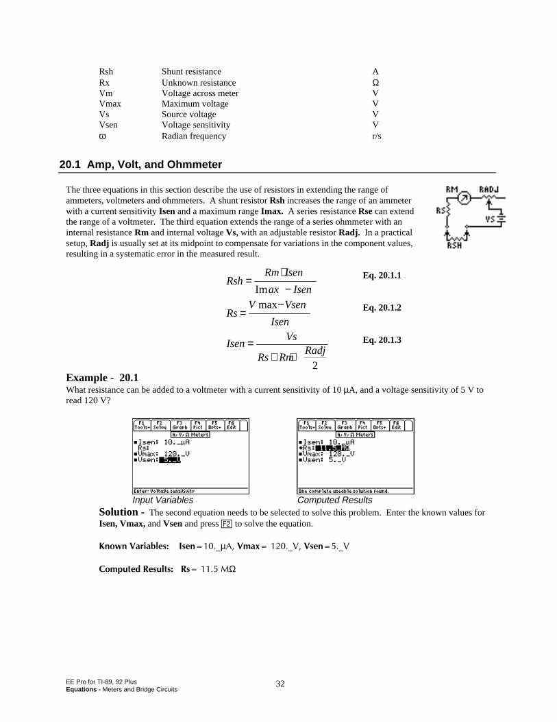
EE Pro for TI-89, 92 PlusEquations - Meters and Bridge Circuits
32
Rsh Shunt resistance ARx Unknown resistance ΩVm Voltage across meter VVmax Maximum voltage VVs Source voltage VVsen Voltage sensitivity Vω Radian frequency r/s
20.1 Amp, Volt, and Ohmmeter
The three equations in this section describe the use of resistors in extending the range ofammeters, voltmeters and ohmmeters. A shunt resistor Rsh increases the range of an ammeterwith a current sensitivity Isen and a maximum range Imax. A series resistance Rse can extendthe range of a voltmeter. The third equation extends the range of a series ohmmeter with aninternal resistance Rm and internal voltage Vs, with an adjustable resistor Radj. In a practicalsetup, Radj is usually set at its midpoint to compensate for variations in the component values,resulting in a systematic error in the measured result.
Eq. 20.1.1
Eq. 20.1.2
Eq. 20.1.3
Example - 20.1What resistance can be added to a voltmeter with a current sensitivity of 10 µA, and a voltage sensitivity of 5 V toread 120 V?
Input Variables Computed ResultsSolution - The second equation needs to be selected to solve this problem. Enter the known values forIsen, Vmax, and Vsen and press „ to solve the equation.
-PQYP8CTKCDNGU+UGPAµ#8OCZA88UGPA8
%QORWVGF4GUWNVU4U/Ω
RshRm Isen
ax Isen=
⋅−Im
RsV Vsen
Isen=
−max
IsenVs
Rs RmRadj
=+ +
2
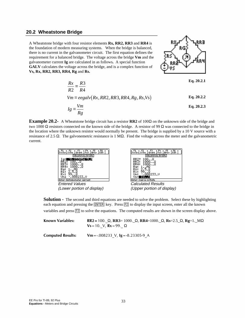
EE Pro for TI-89, 92 PlusEquations - Meters and Bridge Circuits
33
20.2 Wheatstone Bridge
A Wheatstone bridge with four resistor elements Rx, RR2, RR3 and RR4 isthe foundation of modern measuring systems. When the bridge is balanced,there is no current in the galvanometer circuit. The first equation defines therequirement for a balanced bridge. The voltage across the bridge Vm and thegalvanometer current Ig are calculated in as follows. A special functionGALV calculates the voltage across the bridge, and is a complex function ofVs, Rx, RR2, RR3, RR4, Rg and Rs.
Eq. 20.2.1
Eq. 20.2.2
Eq. 20.2.3
Example 20.2- A Wheatstone bridge circuit has a resistor RR2 of 100Ω on the unknown side of the bridge andtwo 1000 Ω resistors connected on the known side of the bridge. A resistor of 99 Ω was connected to the bridge inthe location where the unknown resistor would normally be present. The bridge is supplied by a 10 V source with aresistance of 2.5 Ω. The galvonemetric resistance is 1 MΩ. Find the voltage across the meter and the galvanometriccurrent.
Entered Values Calculated Results(Lower portion of display) (Upper portion of display)
Solution - The second and third equations are needed to solve the problem. Select these by highlightingeach equation and pressing the key. Press „ to display the input screen, enter all the known
variables and press „ to solve the equations. The computed results are shown in the screen display above.
-PQYP8CTKCDNGU 44AΩ, RR3= 1000._Ω, RR4=1000._Ω, Rs=2.5_Ω, Rg=1._MΩ8UA84ZA Ω
%QORWVGF4GUWNVU 8OA8+IA#
Rx
R
R
R2
3
4=
Vm eegalv Rx RR RR RR Rg Rs Vs= , , , , , ,2 3 4b gIg
Vm
Rg=
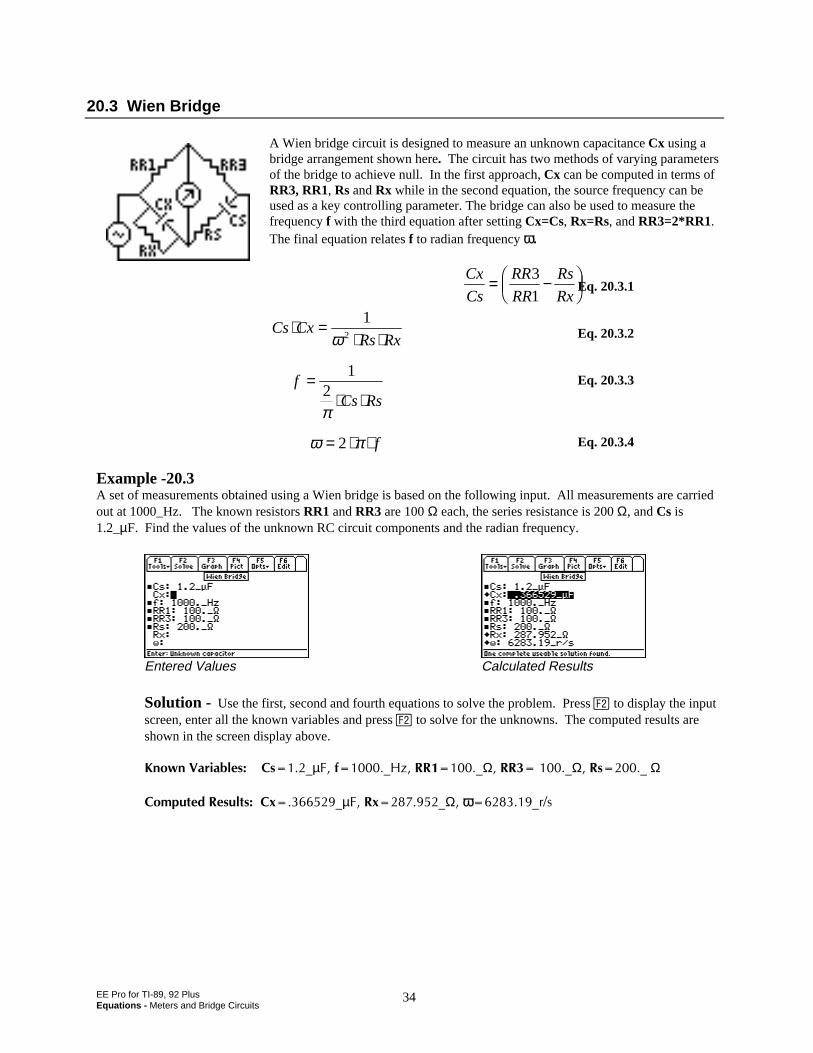
EE Pro for TI-89, 92 PlusEquations - Meters and Bridge Circuits
34
20.3 Wien Bridge
A Wien bridge circuit is designed to measure an unknown capacitance Cx using abridge arrangement shown here. The circuit has two methods of varying parametersof the bridge to achieve null. In the first approach, Cx can be computed in terms ofRR3, RR1, Rs and Rx while in the second equation, the source frequency can beused as a key controlling parameter. The bridge can also be used to measure thefrequency f with the third equation after setting Cx=Cs, Rx=Rs, and RR3=2*RR1.The final equation relates f to radian frequency ω.
Eq. 20.3.1
Eq. 20.3.2
Eq. 20.3.3
Eq. 20.3.4
Example -20.3A set of measurements obtained using a Wien bridge is based on the following input. All measurements are carriedout at 1000_Hz. The known resistors RR1 and RR3 are 100 Ω each, the series resistance is 200 Ω, and Cs is1.2_µF. Find the values of the unknown RC circuit components and the radian frequency.
Entered Values Calculated Results
Solution - Use the first, second and fourth equations to solve the problem. Press „ to display the inputscreen, enter all the known variables and press „ to solve for the unknowns. The computed results areshown in the screen display above.
-PQYP8CTKCDNGU%UAµ(HA*\44AΩ44AΩ4UA Ω
%QORWVGF4GUWNVU%ZAµ(4ZAΩωωATU
Cx
Cs
RR
RR
Rs
Rx= −FHG
IKJ
3
1
Cs CxRs Rx
⋅ =⋅ ⋅
12ω
fCs Rs
=⋅ ⋅
12π
ω π= ⋅ ⋅2 f
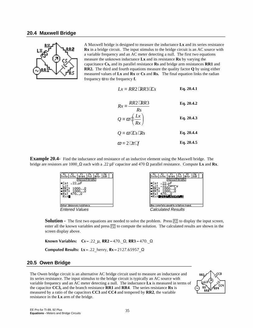
EE Pro for TI-89, 92 PlusEquations - Meters and Bridge Circuits
35
20.4 Maxwell Bridge
A Maxwell bridge is designed to measure the inductance Lx and its series resistanceRx in a bridge circuit. The input stimulus to the bridge circuit is an AC source witha variable frequency and an AC meter detecting a null. The first two equationsmeasure the unknown inductance Lx and its resistance Rx by varying thecapacitance Cs, and its parallel resistance Rs and bridge arm resistances RR1 andRR2. The third and fourth equations measure the quality factor Q by using eithermeasured values of Lx and Rx or Cs and Rs. The final equation links the radianfrequency ω to the frequency f.
Eq. 20.4.1
Eq. 20.4.2
Eq. 20.4.3
Eq. 20.4.4
Eq. 20.4.5
Example 20.4- Find the inductance and resistance of an inductive element using the Maxwell bridge. Thebridge are resistors are 1000_Ω each with a .22 µF capacitor and 470 Ω parallel resistance. Compute Lx and Rx.
Entered Values Calculated Results
Solution - The first two equations are needed to solve the problem. Press „ to display the input screen,enter all the known variables and press „ to compute the solution. The calculated results are shown in thescreen display above.
-PQYP8CTKCDNGU%UAµ44AΩ44AΩ
%QORWVGF4GUWNVU.ZAJGPT[4ZAΩ
20.5 Owen Bridge
The Owen bridge circuit is an alternative AC bridge circuit used to measure an inductance andits series resistance. The input stimulus to the bridge circuit is typically an AC source withvariable frequency and an AC meter detecting a null. The inductance Lx is measured in terms ofthe capacitor CC3, and the branch resistance RR1 and RR4. The series resistance Rx ismeasured by a ratio of the capacitors CC3 and CC4 and tempered by RR2, the variableresistance in the Lx arm of the bridge.
Lx RR RR Cs= ⋅ ⋅2 3
RxRR RR
Rs= ⋅2 3
Q Cs Rs= ⋅ ⋅ω
QLx
Rx= ⋅FHG
IKJω
ω π= ⋅ ⋅2 f
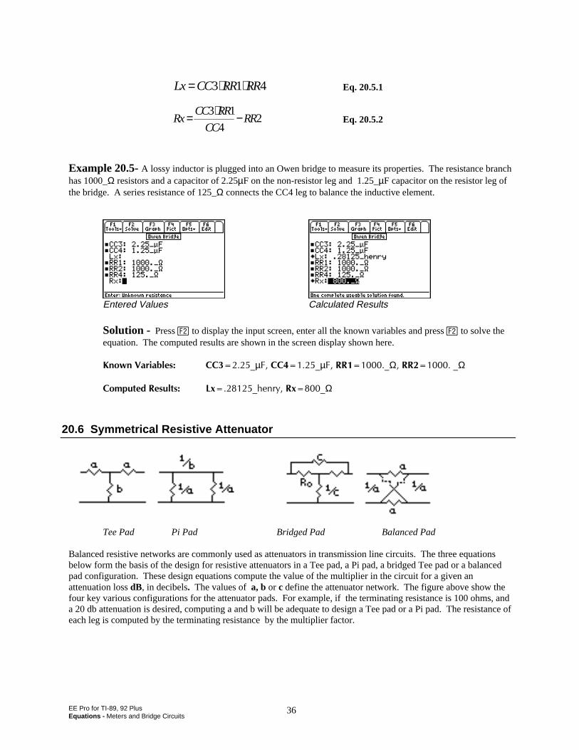
EE Pro for TI-89, 92 PlusEquations - Meters and Bridge Circuits
36
Lx CC RR RR= ⋅ ⋅3 1 4 Eq. 20.5.1
RxCC RR
CCRR= ⋅ −3 1
42 Eq. 20.5.2
Example 20.5- A lossy inductor is plugged into an Owen bridge to measure its properties. The resistance branchhas 1000_Ω resistors and a capacitor of 2.25µF on the non-resistor leg and 1.25_µF capacitor on the resistor leg ofthe bridge. A series resistance of 125_Ω connects the CC4 leg to balance the inductive element.
Entered Values Calculated Results
Solution - Press „ to display the input screen, enter all the known variables and press „ to solve theequation. The computed results are shown in the screen display shown here.
-PQYP8CTKCDNGU %%Aµ(%%Aµ(44AΩ44AΩ
%QORWVGF4GUWNVU .ZAJGPT[4ZAΩ
20.6 Symmetrical Resistive Attenuator
Tee Pad Pi Pad Bridged Pad Balanced Pad
Balanced resistive networks are commonly used as attenuators in transmission line circuits. The three equationsbelow form the basis of the design for resistive attenuators in a Tee pad, a Pi pad, a bridged Tee pad or a balancedpad configuration. These design equations compute the value of the multiplier in the circuit for a given anattenuation loss dB, in decibels. The values of a, b or c define the attenuator network. The figure above show thefour key various configurations for the attenuator pads. For example, if the terminating resistance is 100 ohms, anda 20 db attenuation is desired, computing a and b will be adequate to design a Tee pad or a Pi pad. The resistance ofeach leg is computed by the terminating resistance by the multiplier factor.
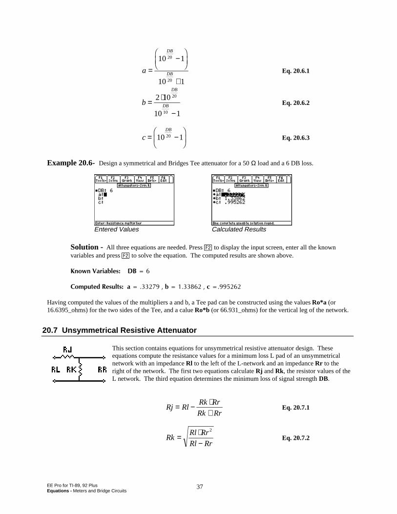
EE Pro for TI-89, 92 PlusEquations - Meters and Bridge Circuits
37
a
DB
DB=−
FHG
IKJ
+
10 1
10 1
20
20
Eq. 20.6.1
b
DB
DB= ⋅
−
2 10
10 1
20
10
Eq. 20.6.2
cDB
= −FHG
IKJ10 120 Eq. 20.6.3
Example 20.6- Design a symmetrical and Bridges Tee attenuator for a 50 Ω load and a 6 DB loss.
Entered Values Calculated Results
Solution - All three equations are needed. Press „ to display the input screen, enter all the knownvariables and press „ to solve the equation. The computed results are shown above.
-PQYP8CTKCDNGU&$
%QORWVGF4GUWNVUCDE
Having computed the values of the multipliers a and b, a Tee pad can be constructed using the values Ro*a (or16.6395_ohms) for the two sides of the Tee, and a calue Ro*b (or 66.931_ohms) for the vertical leg of the network.
20.7 Unsymmetrical Resistive Attenuator
This section contains equations for unsymmetrical resistive attenuator design. Theseequations compute the resistance values for a minimum loss L pad of an unsymmetricalnetwork with an impedance Rl to the left of the L-network and an impedance Rr to theright of the network. The first two equations calculate Rj and Rk, the resistor values of theL network. The third equation determines the minimum loss of signal strength DB.
Rj RlRk Rr
Rk Rr= − ⋅
+Eq. 20.7.1
RkRl Rr
Rl Rr= ⋅
−
2
Eq. 20.7.2
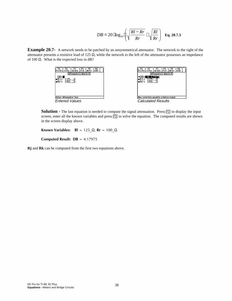
EE Pro for TI-89, 92 PlusEquations - Meters and Bridge Circuits
38
DBRl Rr
Rr
Rl
Rr= ⋅ ⋅ − +
FHG
IKJ20 10log Eq. 20.7.3
Example 20.7- A network needs to be patched by an unsymmetrical attenuator. The network to the right of theattenuator presents a resistive load of 125 Ω, while the network to the left of the attenuator possesses an impedanceof 100 Ω. What is the expected loss in dB?
Entered Values Calculated Results
Solution - The last equation is needed to compute the signal attenuation. Press „ to display the inputscreen, enter all the known variables and press „ to solve the equation. The computed results are shownin the screen display above.
-PQYP8CTKCDNGU4NAΩ4TAΩ
%QORWVGF4GUWNV&$
Rj and Rk can be computed from the first two equations above.
EE PRO for TI -89, 92 PlusEquations - RL and RC Circuits
39
Chapter 21 RL and RC CircuitsThis chapter covers the natural and transient properties of simple RL and RC circuits. The section is organizedunder six topics.
RL Natural ResponseRC Natural ResponseRL Step Response
RC Step ResponseRL Series to ParallelRC Series to Parallel
Variables
The table below lists all the variables used in this chapter, along with a brief description and appropriate units.
Variable Description UnitC Capacitor FCs Series capacitance FCp Parallel capacitance Ff Frequency HziC Capacitor current AiL Inductor current AI0 Initial inductor current AL Inductance HLp Parallel inductance HLs Series inductance HQp Q, parallel circuit unitlessQs Q, series circuit unitlessR Resistance ΩRp Parallel resistance ΩRs Series resistance Ωτ Time constant st Time svC Capacitor voltage VvL Inductor voltage VV0 Initial capacitor voltage VVs Voltage stimulus Vω Radian frequency r/sW Energy dissipated J
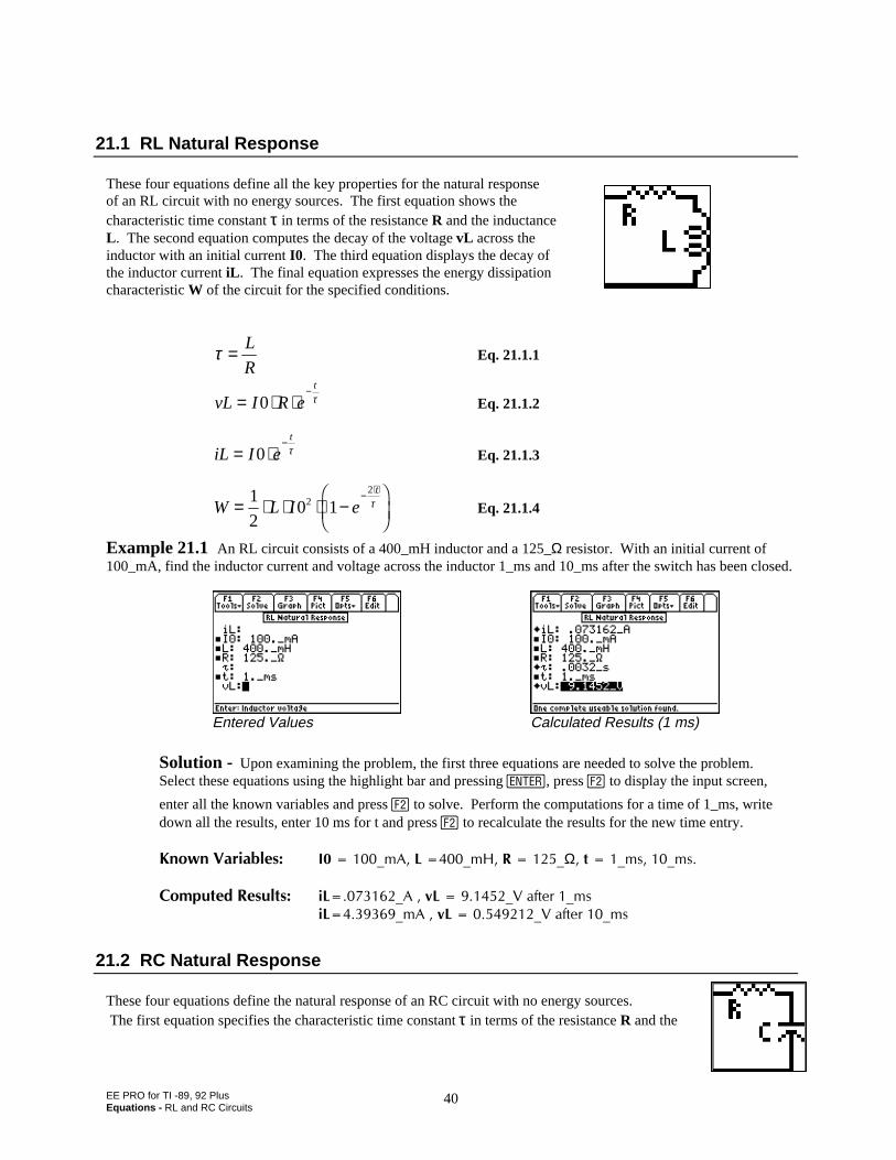
EE PRO for TI -89, 92 PlusEquations - RL and RC Circuits
40
21.1 RL Natural Response
These four equations define all the key properties for the natural responseof an RL circuit with no energy sources. The first equation shows thecharacteristic time constant τ in terms of the resistance R and the inductanceL . The second equation computes the decay of the voltage vL across theinductor with an initial current I0. The third equation displays the decay ofthe inductor current iL . The final equation expresses the energy dissipationcharacteristic W of the circuit for the specified conditions.
τ = L
REq. 21.1.1
vL I R et
= ⋅ ⋅−
0 τ Eq. 21.1.2
iL I et
= ⋅−
0 τ Eq. 21.1.3
W L I et
= ⋅ ⋅ ⋅ −FHG
IKJ
− ⋅1
20 12
2
τ Eq. 21.1.4
Example 21.1 An RL circuit consists of a 400_mH inductor and a 125_Ω resistor. With an initial current of100_mA, find the inductor current and voltage across the inductor 1_ms and 10_ms after the switch has been closed.
Entered Values Calculated Results (1 ms)
Solution - Upon examining the problem, the first three equations are needed to solve the problem.Select these equations using the highlight bar and pressing , press „ to display the input screen,
enter all the known variables and press „ to solve. Perform the computations for a time of 1_ms, writedown all the results, enter 10 ms for t and press „ to recalculate the results for the new time entry.
-PQYP8CTKCDNGU +AO#.AO*4AΩVAOUAOU
%QORWVGF4GUWNVU K.A#X.A8CHVGTAOUK.AO#X.A8CHVGTAOU
21.2 RC Natural Response
These four equations define the natural response of an RC circuit with no energy sources. The first equation specifies the characteristic time constant τ in terms of the resistance R and the
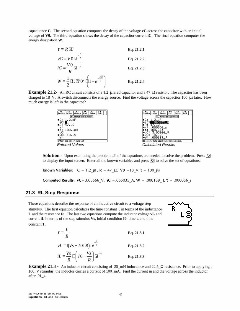
EE PRO for TI -89, 92 PlusEquations - RL and RC Circuits
41
capacitance C. The second equation computes the decay of the voltage vC across the capacitor with an initialvoltage of V0. The third equation shows the decay of the capacitor current iC. The final equation computes theenergy dissipation W.
τ = ⋅R C Eq. 21.2.1
vC V et
= ⋅−
0 τ Eq. 21.2.2
iCV
Re
t
= ⋅−0 τ Eq. 21.2.3
W C V et
= ⋅ ⋅ ⋅ −FHG
IKJ
− ⋅1
20 12
2
τ Eq. 21.2.4
Example 21.2- An RC circuit consists of a 1.2_µfarad capacitor and a 47_Ω resistor. The capacitor has beencharged to 18_V. A switch disconnects the energy source. Find the voltage across the capacitor 100_µs later. Howmuch energy is left in the capacitor?
Entered Values Calculated Results
Solution - Upon examining the problem, all of the equations are needed to solve the problem. Press „
to display the input screen. Enter all the known variables and press „ to solve the set of equations.
-PQYP8CTKCDNGU%Aµ(4AΩ8A8VAµU
%QORWVGF4GUWNVUX%A8K%A#9A,τAU
21.3 RL Step Response
These equations describe the response of an inductive circuit to a voltage step
stimulus. The first equation calculates the time constant τ in terms of the inductanceL and the resistance R. The last two equations compute the inductor voltage vL andcurrent iL in terms of the step stimulus Vs, initial condition I0, time t, and time
constant τ.
τ = L
REq. 21.3.1
vL Vs I R et
= ⋅ − ⋅ ⋅−
0b g τ Eq. 21.3.2
iLVs
RI
Vs
Re
t
= + −FHG
IKJ ⋅
−0 τ Eq. 21.3.3
Example 21.3 - An inductor circuit consisting of 25_mH inductance and 22.5_Ω resistance. Prior to applying a100_V stimulus, the inductor carries a current of 100_mA. Find the current in and the voltage across the inductorafter .01_s.
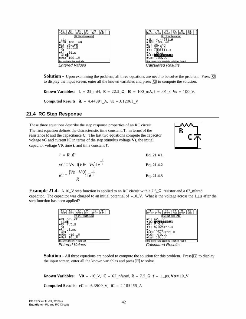
EE PRO for TI -89, 92 PlusEquations - RL and RC Circuits
42
Entered Values Calculated Results
Solution - Upon examining the problem, all three equations are need to be solve the problem. Press „
to display the input screen, enter all the known variables and press „ to compute the solution.
-PQYP8CTKCDNGU.AO*4AΩ+AO#VAU8UA8
%QORWVGF4GUWNVUK.A#X.A8
21.4 RC Step Response
These three equations describe the step response properties of an RC circuit.The first equation defines the characteristic time constant, ττ, in terms of theresistance R and the capacitance C. The last two equations compute the capacitorvoltage vC and current iC in terms of the step stimulus voltage Vs, the initialcapacitor voltage V0, time t, and time constant ττ.
τ = ⋅R C Eq. 21.4.1
vC Vs V Vs et
= + − ⋅−
0b g τ Eq. 21.4.2
iCVs V
Re
t
=−
⋅−0b g τ Eq. 21.4.3
Example 21.4- A 10_V step function is applied to an RC circuit with a 7.5_Ω resistor and a 67_nfaradcapacitor. The capacitor was charged to an initial potential of –10_V. What is the voltage across the.1_µs after thestep function has been applied?
Entered Values Calculated Results
Solution - All three equations are needed to compute the solution for this problem. Press „ to displaythe input screen, enter all the known variables and press „ to solve.
-PQYP8CTKCDNGU8A8%APHCTCF4AΩV.1_µs, Vs = 10_V
%QORWVGF4GUWNVUX%A8K%A#
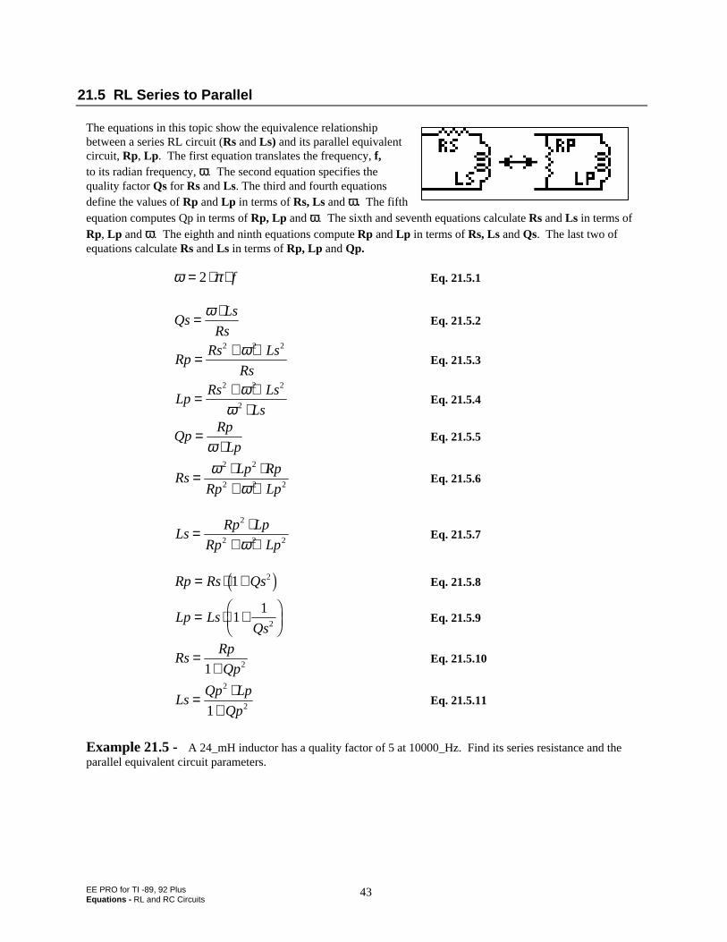
EE PRO for TI -89, 92 PlusEquations - RL and RC Circuits
43
21.5 RL Series to Parallel
The equations in this topic show the equivalence relationshipbetween a series RL circuit (Rs and Ls) and its parallel equivalentcircuit, Rp, Lp. The first equation translates the frequency, f,to its radian frequency, ω. The second equation specifies thequality factor Qs for Rs and Ls. The third and fourth equationsdefine the values of Rp and Lp in terms of Rs, Ls and ω. The fifthequation computes Qp in terms of Rp, Lp and ω. The sixth and seventh equations calculate Rs and Ls in terms ofRp, Lp and ω. The eighth and ninth equations compute Rp and Lp in terms of Rs, Ls and Qs. The last two ofequations calculate Rs and Ls in terms of Rp, Lp and Qp.
ω π= ⋅ ⋅2 f Eq. 21.5.1
QsLs
Rs= ⋅ω
Eq. 21.5.2
RpRs Ls
Rs= + ⋅2 2 2ω
Eq. 21.5.3
LpRs Ls
Ls= + ⋅
⋅
2 2 2
2
ωω
Eq. 21.5.4
QpRp
Lp=
⋅ωEq. 21.5.5
RsLp Rp
Rp Lp= ⋅ ⋅
+ ⋅ω
ω
2 2
2 2 2Eq. 21.5.6
LsRp Lp
Rp Lp= ⋅
+ ⋅
2
2 2 2ωEq. 21.5.7
Rp Rs Qs= ⋅ +1 2c h Eq. 21.5.8
Lp LsQs
= ⋅ +FHG
IKJ1
12
Eq. 21.5.9
RsRp
Qp=
+1 2Eq. 21.5.10
LsQp Lp
Qp= ⋅
+
2
21Eq. 21.5.11
Example 21.5 - A 24_mH inductor has a quality factor of 5 at 10000_Hz. Find its series resistance and theparallel equivalent circuit parameters.
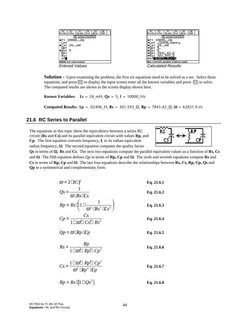
EE PRO for TI -89, 92 PlusEquations - RL and RC Circuits
44
Entered Values Calculated Results
Solution - Upon examining the problem, the first six equations need to be solved as a set. Select theseequations, and press „ to display the input screen enter all the known variables and press „ to solve.The computed results are shown in the screen display shown here.
-PQYP8CTKCDNGU.UAO*3UHA*\
%QORWVGF4GUWNVU.RA*4UAΩ4RAΩωωTU
21.6 RC Series to Parallel
The equations in this topic show the equivalence between a series RCcircuit (Rs and Cs) and its parallel equivalent circuit with values Rp, andCp. The first equation converts frequency, f, to its radian equivalentradian frequency, ω. The second equation computes the quality factorQs in terms of ω, Rs and Cs. The next two equations compute the parallel equivalent values as a function of Rs, Csand ω. The fifth equation defines Qp in terms of Rp, Cp and ω. The sixth and seventh equations compute Rs andCs in terms of Rp, Cp and ω. The last four equations describe the relationships between Rs, Cs, Rp, Cp, Qs andQp in a symmetrical and complementary form.
ω π= ⋅ ⋅2 f Eq. 21.6.1
QsRs Cs
=⋅ ⋅
1
ωEq. 21.6.2
Rp RsRs Cs
= ⋅ +⋅ ⋅
FHG
IKJ1
12 2 2ω
Eq. 21.6.3
CpCs
Cs Rs=
+ ⋅ ⋅1 2 2 2ωEq. 21.6.4
Qp Rp Cp= ⋅ ⋅ω Eq. 21.6.5
RsRp
Rp Cp=
+ ⋅ ⋅1 2 2 2ωEq. 21.6.6
CsRp Cp
Rp Cp= + ⋅ ⋅
⋅ ⋅1 2 2 2
2 2
ωω
Eq. 21.6.7
Rp Rs Qs= ⋅ +1 2c h Eq. 21.6.8
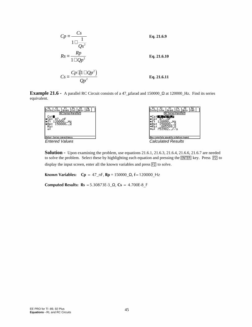
EE PRO for TI -89, 92 PlusEquations - RL and RC Circuits
45
CpCs
Qs
=+1
12
Eq. 21.6.9
RsRp
Qp=
+1 2Eq. 21.6.10
CsCp Qp
Qp=
⋅ +1 2
2
c hEq. 21.6.11
Example 21.6 - A parallel RC Circuit consists of a 47_µfarad and 150000_Ω at 120000_Hz. Find its seriesequivalent.
Entered Values Calculated Results
Solution - Upon examining the problem, use equations 21.6.1, 21.6.3, 21.6.4, 21.6.6, 21.6.7 are neededto solve the problem. Select these by highlighting each equation and pressing the ¸ key. Press „ to
display the input screen, enter all the known variables and press „ to solve.
-PQYP8CTKCDNGU%R_P(, 4R = 150000_Ω, HA*\
%QORWVGF4GUWNVU4U'_Ω%U'A(
EE Pro for TI-89, 92 PlusEquations – RLC Circuits
46
Chapter 22 RLC CircuitsThe essential equations for computing impedance and admittance, natural response, and transient behavior of RLCcircuits are organized into six topics.
Series ImpedanceParallel AdmittanceRLC Natural Response
Underdamped TransientCritically-Damped TransientOverdamped Transient
Variables
All the variables used here are listed along with a brief description and units.
Variable Description Unitα Neper’s frequency rad/sA1 Constant VA2 Constant VB Susceptance SB1 Constant VB2 Constant VBC Capacitive susceptance SBL Inductive susceptance SC Capacitance FD1 Constant V/sD2 Constant Vf Frequency HzG Conductance SI0 Initial inductor current AL Inductance Hθ Phase angle radR Resistance Ωs1 Characteristic frequency rad/ss2 Characteristic frequency rad/ss1i Characteristic frequency (imaginary) rad/ss1r Characteristic frequency (real) rad/ss2i Characteristic frequency (imaginary) rad/ss2i Characteristic frequency (real) rad/st Time sv Capacitor voltage VV0 Initial capacitor voltage Vω Radian Frequency rad/sωd Damped radian frequency rad/s
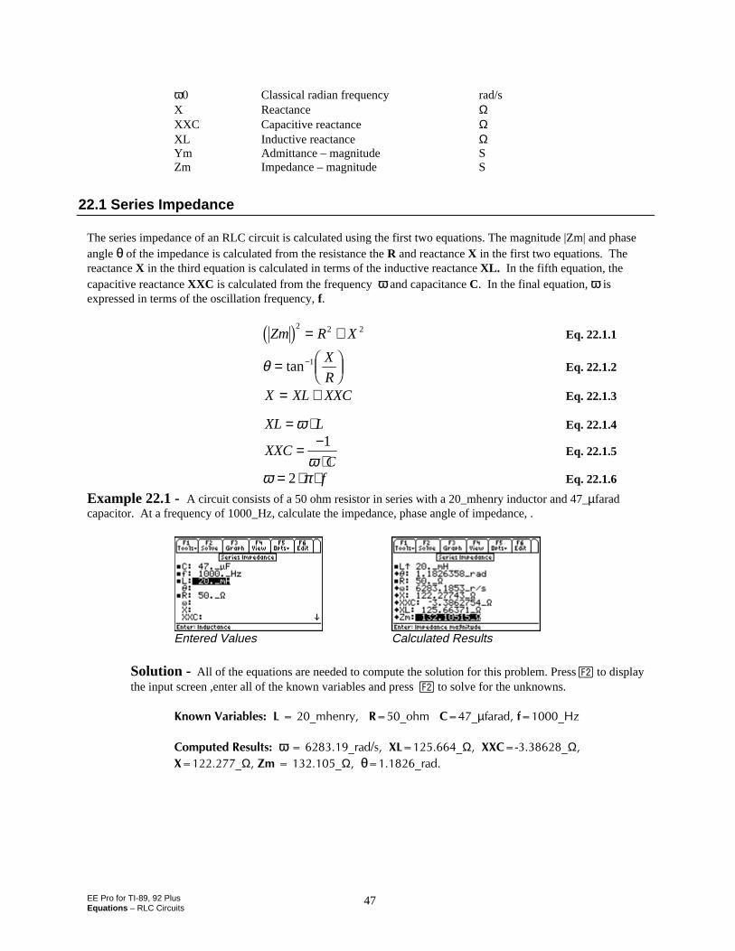
EE Pro for TI-89, 92 PlusEquations – RLC Circuits
47
ω0 Classical radian frequency rad/sX Reactance ΩXXC Capacitive reactance ΩXL Inductive reactance ΩYm Admittance – magnitude SZm Impedance – magnitude S
22.1 Series Impedance
The series impedance of an RLC circuit is calculated using the first two equations. The magnitude |Zm| and phaseangle θ of the impedance is calculated from the resistance the R and reactance X in the first two equations. Thereactance X in the third equation is calculated in terms of the inductive reactance XL. In the fifth equation, thecapacitive reactance XXC is calculated from the frequency ω and capacitance C. In the final equation, ω isexpressed in terms of the oscillation frequency, f.
Zm R Xc h2 2 2= + Eq. 22.1.1
θ = FHG
IKJ
−tan 1 X
REq. 22.1.2
X XL XXC= + Eq. 22.1.3
XL L= ⋅ω Eq. 22.1.4
XXCC
= −⋅1
ωEq. 22.1.5
ω π= ⋅ ⋅2 f Eq. 22.1.6
Example 22.1 - A circuit consists of a 50 ohm resistor in series with a 20_mhenry inductor and 47_µfaradcapacitor. At a frequency of 1000_Hz, calculate the impedance, phase angle of impedance, .
Entered Values Calculated Results
Solution - All of the equations are needed to compute the solution for this problem. Press „ to displaythe input screen ,enter all of the known variables and press „ to solve for the unknowns.
-PQYP8CTKCDNGU.AOJGPT[4AQJO%AµHCTCFHA*\
%QORWVGF4GUWNVUωATCFU:.AΩ::%AΩ
:AΩ<OAΩθθATCF
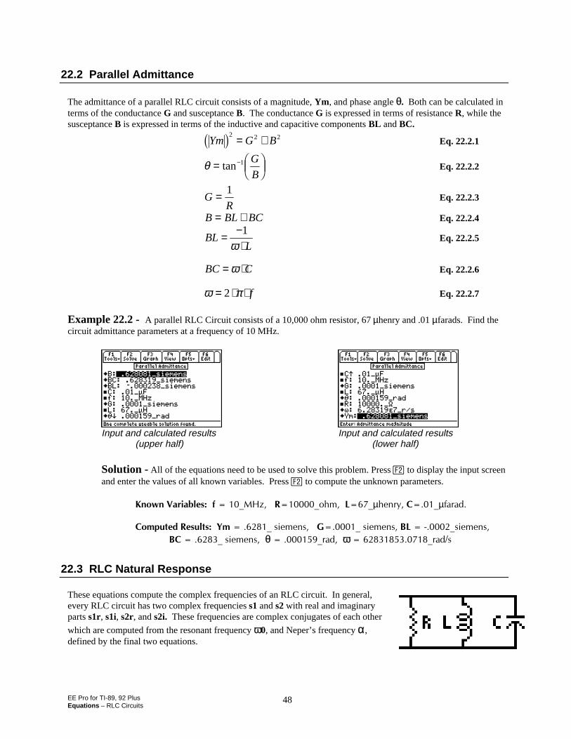
EE Pro for TI-89, 92 PlusEquations – RLC Circuits
48
22.2 Parallel Admittance
The admittance of a parallel RLC circuit consists of a magnitude, Ym, and phase angle θ. Both can be calculated interms of the conductance G and susceptance B. The conductance G is expressed in terms of resistance R, while thesusceptance B is expressed in terms of the inductive and capacitive components BL and BC.
Ym G Bc h2 2 2= + Eq. 22.2.1
θ = FHG
IKJ
−tan 1 G
BEq. 22.2.2
GR
= 1Eq. 22.2.3
B BL BC= + Eq. 22.2.4
BLL
= −⋅1
ωEq. 22.2.5
BC C= ⋅ω Eq. 22.2.6
ω π= ⋅ ⋅2 f Eq. 22.2.7
Example 22.2 - A parallel RLC Circuit consists of a 10,000 ohm resistor, 67 µhenry and .01 µfarads. Find thecircuit admittance parameters at a frequency of 10 MHz.
Input and calculated results Input and calculated results(upper half) (lower half)
Solution - All of the equations need to be used to solve this problem. Press „ to display the input screenand enter the values of all known variables. Press „ to compute the unknown parameters.
-PQYP8CTKCDNGUHA/*\4AQJO.AµJGPT[%AµHCTCF
%QORWVGF4GUWNVU;OAUKGOGPU)AUKGOGPU$.AUKGOGPU
$%AUKGOGPUθATCFωATCFU
22.3 RLC Natural Response
These equations compute the complex frequencies of an RLC circuit. In general,every RLC circuit has two complex frequencies s1 and s2 with real and imaginaryparts s1r, s1i, s2r, and s2i. These frequencies are complex conjugates of each other
which are computed from the resonant frequency ω0, and Neper’s frequency α,defined by the final two equations.
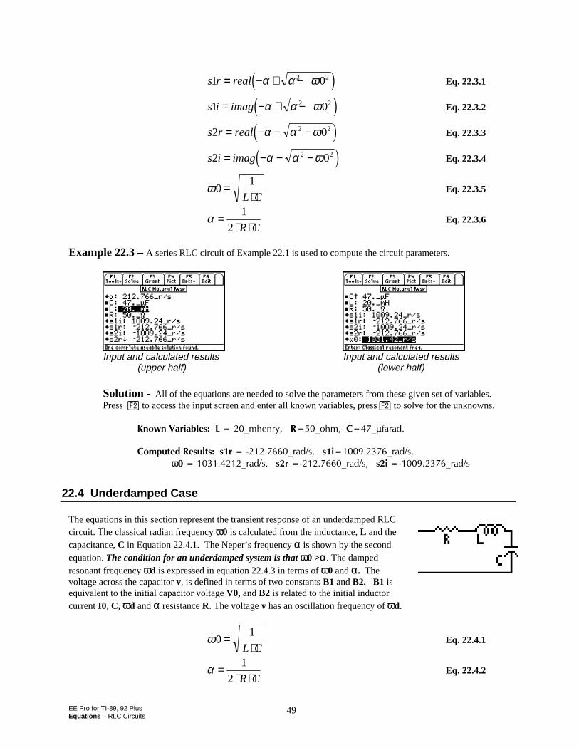
EE Pro for TI-89, 92 PlusEquations – RLC Circuits
49
s r real1 02 2= − + −α α ωe j Eq. 22.3.1
s i imag1 02 2= − + −α α ωe j Eq. 22.3.2
s r real2 02 2= − − −α α ωe j Eq. 22.3.3
s i imag2 02 2= − − −α α ωe j Eq. 22.3.4
ω01=⋅L C
Eq. 22.3.5
α =⋅ ⋅
1
2 R CEq. 22.3.6
Example 22.3 – A series RLC circuit of Example 22.1 is used to compute the circuit parameters.
Input and calculated results Input and calculated results (upper half) (lower half)
Solution - All of the equations are needed to solve the parameters from these given set of variables.Press „ to access the input screen and enter all known variables, press „ to solve for the unknowns.
-PQYP8CTKCDNGU.AOJGPT[4AQJO%AµHCTCF
%QORWVGF4GUWNVUUTATCFUUKATCFU
ωATCFUUTATCFUUKATCFU
22.4 Underdamped Case
The equations in this section represent the transient response of an underdamped RLCcircuit. The classical radian frequency ω0 is calculated from the inductance, L and thecapacitance, C in Equation 22.4.1. The Neper’s frequency α is shown by the secondequation. The condition for an underdamped system is that ω0 >α. The dampedresonant frequency ωd is expressed in equation 22.4.3 in terms of ω0 and α. Thevoltage across the capacitor v, is defined in terms of two constants B1 and B2. B1 isequivalent to the initial capacitor voltage V0, and B2 is related to the initial inductorcurrent I0, C, ωd and α resistance R. The voltage v has an oscillation frequency of ωd.
ω01=⋅L C
Eq. 22.4.1
α =⋅ ⋅
1
2 R CEq. 22.4.2
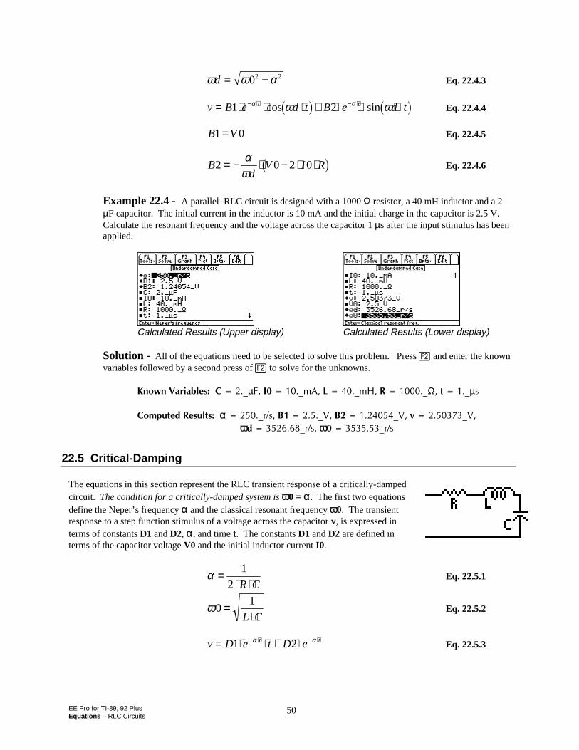
EE Pro for TI-89, 92 PlusEquations – RLC Circuits
50
ω ω αd = −02 2 Eq. 22.4.3
v B e d t B e d tt t= ⋅ ⋅ ⋅ + ⋅ ⋅ ⋅− ⋅ − ⋅1 2α αω ωcos sinb g b g Eq. 22.4.4
B V1 0= Eq. 22.4.5
Bd
V I R2 0 2 0= − ⋅ − ⋅ ⋅αω
b g Eq. 22.4.6
Example 22.4 - A parallel RLC circuit is designed with a 1000 Ω resistor, a 40 mH inductor and a 2µF capacitor. The initial current in the inductor is 10 mA and the initial charge in the capacitor is 2.5 V.Calculate the resonant frequency and the voltage across the capacitor 1 µs after the input stimulus has beenapplied.
Calculated Results (Upper display) Calculated Results (Lower display)
Solution - All of the equations need to be selected to solve this problem. Press „ and enter the knownvariables followed by a second press of „ to solve for the unknowns.
-PQYP8CTKCDNGU%Aµ(+AO#.AO*4AΩVAµU
%QORWVGF4GUWNVUααATU$A8$A8XA8
ωFATUωATU
22.5 Critical-Damping
The equations in this section represent the RLC transient response of a critically-dampedcircuit. The condition for a critically-damped system is ω0 = α. The first two equationsdefine the Neper’s frequency α and the classical resonant frequency ω0. The transientresponse to a step function stimulus of a voltage across the capacitor v, is expressed interms of constants D1 and D2, α, and time t. The constants D1 and D2 are defined interms of the capacitor voltage V0 and the initial inductor current I0.
α =⋅ ⋅
1
2 R CEq. 22.5.1
ω01=⋅L C
Eq. 22.5.2
v D e t D et t= ⋅ ⋅ + ⋅− ⋅ − ⋅1 2α α Eq. 22.5.3
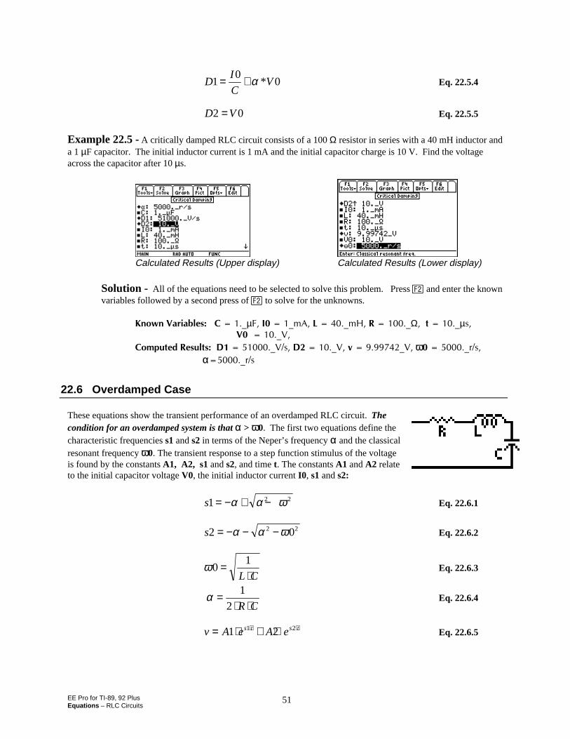
EE Pro for TI-89, 92 PlusEquations – RLC Circuits
51
DI
CV1
00= + α * Eq. 22.5.4
D V2 0= Eq. 22.5.5
Example 22.5 - A critically damped RLC circuit consists of a 100 Ω resistor in series with a 40 mH inductor anda 1 µF capacitor. The initial inductor current is 1 mA and the initial capacitor charge is 10 V. Find the voltageacross the capacitor after 10 µs.
Calculated Results (Upper display) Calculated Results (Lower display)
Solution - All of the equations need to be selected to solve this problem. Press „ and enter the knownvariables followed by a second press of „ to solve for the unknowns.
-PQYP8CTKCDNGU%Aµ(+AO#.AO*4AΩVAµU8A8
%QORWVGF4GUWNVU&A8U&A8XA8ωATU
αATU
22.6 Overdamped Case
These equations show the transient performance of an overdamped RLC circuit. Thecondition for an overdamped system is that α > ω0. The first two equations define thecharacteristic frequencies s1 and s2 in terms of the Neper’s frequency α and the classicalresonant frequency ω0. The transient response to a step function stimulus of the voltageis found by the constants A1, A2, s1 and s2, and time t. The constants A1 and A2 relateto the initial capacitor voltage V0, the initial inductor current I0, s1 and s2:
s1 2 2= − + −α α ω Eq. 22.6.1
s2 02 2= − − −α α ω Eq. 22.6.2
ω01=⋅L C
Eq. 22.6.3
α =⋅ ⋅
1
2 R CEq. 22.6.4
v A e A es t s t= ⋅ + ⋅⋅ ⋅1 21 2 Eq. 22.6.5
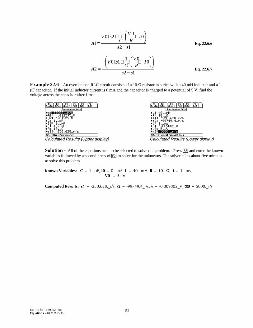
EE Pro for TI-89, 92 PlusEquations – RLC Circuits
52
AV s
C
V
RI
s s1
0 21 0
0
2 1=
⋅ + ⋅ +FHG
IKJ
−Eq. 22.6.6
A
V sC
V
RI
s s2
0 11 0
0
2 1=
− ⋅ + ⋅ +FHG
IKJ
FHG
IKJ
−Eq. 22.6.7
Example 22.6 - An overdamped RLC circuit consists of a 10 Ω resistor in series with a 40 mH inductor and a 1µF capacitor. If the initial inductor current is 0 mA and the capacitor is charged to a potential of 5 V, find thevoltage across the capacitor after 1 ms.
Calculated Results (Upper display) Calculated Results (Lower display)
Solution - All of the equations need to be selected to solve this problem. Press „ and enter the knownvariables followed by a second press of „ to solve for the unknowns. The solver takes about five minutesto solve this problem.
-PQYP8CTKCDNGU%Aµ(+AO#.AO*4AΩVAOU8A8
%QORWVGF4GUWNVUUATUUATUXA8ωωATU
EE Pro for TI-89, 92 PlusEquations - AC Circuits
53
Chapter 23 AC CircuitsThis chapter covers equations describing the properties of AC circuits.
♦ RL Series Impedance♦ RC Series Impedance♦ Impedance ↔ Admittance
♦ Two Impedances in Series♦ Two Impedances in Parallel
Variables
All the variables here are listed with a brief description and appropriate units.
Variable Description UnitC Capacitance Ff Frequency HzI Instantaneous current AIm Current amplitude AL Inductance Hθ Impedance phase angle radθ1 Phase angle 1 radθ2 Phase angle 2 rR Resistance ΩRR1 Resistance 1 ΩRR2 Resistance 2 Ωt Time sV Total voltage VVC Voltage across capacitor VVL Voltage across inductor VVm Maximum voltage VVR Voltage across resistor Vω Radian frequency r/sX Reactance ΩXX1 Reactance 1 ΩXX2 Reactance 2 ΩY_ Admittance SZ1m Impedance 1 magnitude ΩZ2m Impedance 2 magnitude ΩZ_ Complex impedance ΩZm Impedance magnitude Ω
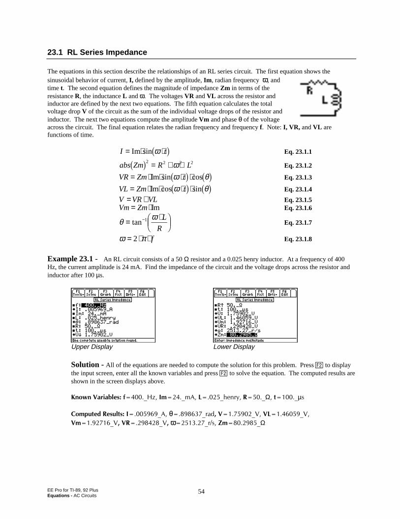
EE Pro for TI-89, 92 PlusEquations - AC Circuits
54
23.1 RL Series Impedance
The equations in this section describe the relationships of an RL series circuit. The first equation shows thesinusoidal behavior of current, I, defined by the amplitude, Im , radian frequency ω, andtime t. The second equation defines the magnitude of impedance Zm in terms of theresistance R, the inductance L and ω. The voltages VR and VL across the resistor andinductor are defined by the next two equations. The fifth equation calculates the totalvoltage drop V of the circuit as the sum of the individual voltage drops of the resistor andinductor. The next two equations compute the amplitude Vm and phase θ of the voltageacross the circuit. The final equation relates the radian frequency and frequency f. Note: I, VR, and VL arefunctions of time.
I t= ⋅ ⋅Im sin ωb g Eq. 23.1.1
abs Zm R Lb g2 2 2 2= + ⋅ω Eq. 23.1.2
VR Zm t= ⋅ ⋅ ⋅ ⋅Im sin cosω θb g b g Eq. 23.1.3
VL Zm t= ⋅ ⋅ ⋅ ⋅Im cos sinω θb g b g Eq. 23.1.4
V VR VL= + Eq. 23.1.5Vm Zm= ⋅ Im Eq. 23.1.6
θ ω= ⋅FHG
IKJ
−tan 1 L
REq. 23.1.7
ω π= ⋅ ⋅2 f Eq. 23.1.8
Example 23.1 - An RL circuit consists of a 50 Ω resistor and a 0.025 henry inductor. At a frequency of 400Hz, the current amplitude is 24 mA. Find the impedance of the circuit and the voltage drops across the resistor andinductor after 100 µs.
Upper Display Lower Display
Solution - All of the equations are needed to compute the solution for this problem. Press „ to displaythe input screen, enter all the known variables and press „ to solve the equation. The computed results areshown in the screen displays above.
-PQYP8CTKCDNGUHA*\+OAO#.AJGPT[4AΩVAµU
%QORWVGF4GUWNVU+A#θATCF8A88.A8
8OA884A8ωATU<OAΩ
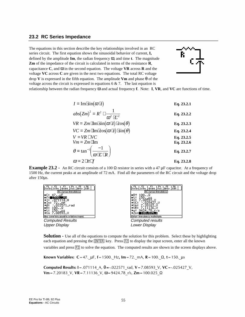
EE Pro for TI-89, 92 PlusEquations - AC Circuits
55
23.2 RC Series Impedance
The equations in this section describe the key relationships involved in an RCseries circuit. The first equation shows the sinusoidal behavior of current, I,defined by the amplitude Im , the radian frequency ω, and time t. The magnitudeZm of the impedance of the circuit is calculated in terms of the resistance R,capacitance C, and ω in the second equation. The voltage VR across R and thevoltage VC across C are given in the next two equations. The total RC voltagedrop V is expressed in the fifth equation. The amplitude Vm and phase θ of thevoltage across the circuit is expressed in equations 6 & 7. The last equation isrelationship between the radian frequency ω and actual frequency f. Note: I , VR, and VC are functions of time.
I t= ⋅ ⋅Im sin ωb g Eq. 23.2.1
abs Zm RC
b g2 22 2
1= +⋅ω
Eq. 23.2.2
VR Zm t= ⋅ ⋅ ⋅ ⋅Im sin cosω θb g b g Eq. 23.2.3
VC Zm t= ⋅ ⋅ ⋅ ⋅Im cos sinω θb g b g Eq. 23.2.4
V VR VC= + Eq. 23.2.5Vm Zm= ⋅ Im Eq. 23.2.6
θω
= −⋅ ⋅
FHG
IKJ
−tan 1 1
C REq. 23.2.7
ω π= ⋅ ⋅2 f Eq. 23.2.8
Example 23.2 - An RC circuit consists of a 100 Ω resistor in series with a 47 µF capacitor. At a frequency of1500 Hz, the current peaks at an amplitude of 72 mA. Find all the parameters of the RC circuit and the voltage dropafter 150µs.
Computed Results Computed resultsUpper Display Lower Display
Solution - Use all of the equations to compute the solution for this problem. Select these by highlightingeach equation and pressing the key. Press „ to display the input screen, enter all the known
variables and press „ to solve the equation. The computed results are shown in the screen displays above.
-PQYP8CTKCDNGU%Aµ(HA*\+OAO#4AΩVAµU
%QORWVGF4GUWNVU+A#θθATCF8A88%A8
8OA884A8ωATU<OAΩ
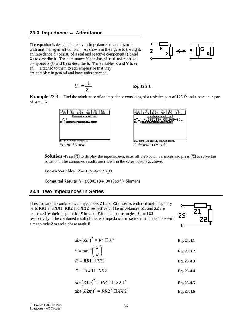
EE Pro for TI-89, 92 PlusEquations - AC Circuits
56
23.3 Impedance ↔ Admittance
The equation is designed to convert impedances to admittanceswith unit management built-in. As shown in the figure to the right,an impedance Z consists of a real and reactive components (R andX) to describe it. The admittance Y consists of real and reactivecomponents (G and B) to describe it. The variables Z and Y havean _ attached to them to add emphasize that theyare complex in general and have units attached.
YZ
__
= 1Eq. 23.3.1
Example 23.3 - Find the admittance of an impedance consisting of a resistive part of 125 Ω and a reactance partof 475_ Ω.
Entered Value Calculated Result
Solution -Press „ to display the input screen, enter all the known variables and press „ to solve theequation. The computed results are shown in the screen displays above.
-PQYP8CTKCDNGU<KAΩ
%QORWVGF4GUWNVU; KA5KGOGPU
23.4 Two Impedances in Series
These equations combine two impedances Z1 and Z2 in series with real and imaginaryparts RR1 and XX1, RR2 and XX2, respectively. The impedances Z1 and Z2 areexpressed by their magnitudes Z1m and Z2m, and phase angles θ1 and θ2respectively. The combined result of the two impedances in series is an impedance witha magnitude Zm and a phase angle θ.
abs Zm R Xb g2 2 2= + Eq. 23.4.1
θ = FHG
IKJ
−tan 1 X
REq. 23.4.2
R RR RR= +1 2 Eq. 23.4.3
X XX XX= +1 2 Eq. 23.4.4
abs Z m RR XX1 1 12 2 2b g = + Eq. 23.4.5
abs Z m RR XX2 2 22 2 2b g = + Eq. 23.4.6
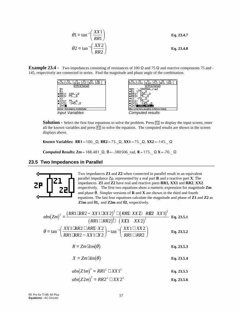
EE Pro for TI-89, 92 PlusEquations - AC Circuits
57
θ11
11= FHG
IKJ
−tanXX
RREq. 23.4.7
θ22
21= FHG
IKJ
−tanXX
RREq. 23.4.8
Example 23.4 - Two impedances consisting of resistances of 100 Ω and 75 Ω and reactive components 75 and -145, respectively are connected in series. Find the magnitude and phase angle of the combination.
Input Variables Computed results
Solution - Select the first four equations to solve the problem. Press „ to display the input screen, enterall the known variables and press „ to solve the equation. The computed results are shown in the screendisplays above.
-PQYP8CTKCDNGU44AΩ44AΩ::AΩ::AΩ
%QORWVGF4GUWNVU<OAΩθθATCF4A Ω:A Ω
23.5 Two Impedances in Parallel
Two impedances Z1 and Z2 when connected in parallel result in an equivalentparallel impedance Zp, represented by a real part R and a reactive part X. Theimpedances Z1 and Z2 have real and reactive parts RR1, XX1 and RR2, XX2respectively. The first two equations show a numeric expression for magnitude Zmand phase θθ. Simpler versions of R and X are shown in the third and fourthequations. The last four equations calculate the magnitude and phase of Z1 and Z2 as
Z1m and θ1, and Z2m and θ2, respectively.
abs ZmRR RR XX XX RR XX RR XX
RR RR XX XXb g b g b g
b g b g2
2 2
2 2
1 2 1 2 1 2 2 1
1 2 1 2=
⋅ − ⋅ + ⋅ + ⋅+ + +
Eq. 23.5.1
θ = ⋅ + ⋅⋅ − ⋅
FHG
IKJ − +
+FHG
IKJ
− −tan tan1 11 2 1 2
1 2 1 2
1 2
1 2
XX RR RR X
RR RR XX X
XX XX
RR RREq. 23.5.2
R Zm= ⋅cosθb g Eq. 23.5.3
X Zm= ⋅sin θb g Eq. 23.5.4
abs Z m RR XX1 1 12 2 2b g = + Eq. 23.5.5
abs Z m RR XX2 2 22 2 2b g = + Eq. 23.5.6
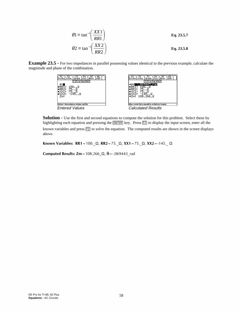
EE Pro for TI-89, 92 PlusEquations - AC Circuits
58
θ11
11= FHG
IKJ
−tanXX
RREq. 23.5.7
θ22
21= FHG
IKJ
−tanXX
RREq. 23.5.8
Example 23.5 - For two impedances in parallel possessing values identical to the previous example, calculate themagnitude and phase of the combination.
Entered Values Calculated Results
Solution - Use the first and second equations to compute the solution for this problem. Select these byhighlighting each equation and pressing the key. Press „ to display the input screen, enter all the
known variables and press „ to solve the equation. The computed results are shown in the screen displaysabove.
-PQYP8CTKCDNGU44AΩ44AΩ::AΩ::AΩ
%QORWVGF4GUWNVU<OAΩθθATCF
EE Pro for TI – 89, 92 PlusEquations – Polyphase circuits
59
Chapter 24 Polyphase CircuitsThis chapter covers equations used in Polyphase circuits. The equations have been divided into three sections.
Balanced ∆ NetworkBalanced Wye Network
Power Measurements
Variables
All the variables are listed below with a brief description and units.
Variable Description UnitIL Line current AIp Phase current AP Power per phase WPT Total power Wθ Impedance angle radVL Line voltage VVp Phase voltage VW1 Wattmeter 1 WW2 Wattmeter 2 W
24.1 Balanced ∆ Network
These equations describe the essential features of a Balanced ∆ Network. The line voltage VL is defined in terms ofphase voltage Vp. The second equation expresses the line current IL using the phase current Ip . The third equationcomputes the power in each phase P from Vp, Ip and the phase delay θ between voltage and current. The last twoequations represent the total power PT delivered to the system in terms of IL, VL Vp and Ip .
VL Vp= Eq. 24.1.1
IL Ip= ⋅3 Eq. 24.1.2
P Vp Ip= ⋅ ⋅cosθb g Eq. 24.1.3
PT Vp Ip= ⋅ ⋅ ⋅3 cosθb g Eq. 24.1.4
PT VL IL= ⋅ ⋅ ⋅3 cosθb g Eq. 24.1.5
Example 24.1 - Given a line current of 25 A, a phase voltage of 110 V, and a phase angle of 0.125 rad, find thephase current, power, total power and line voltage.
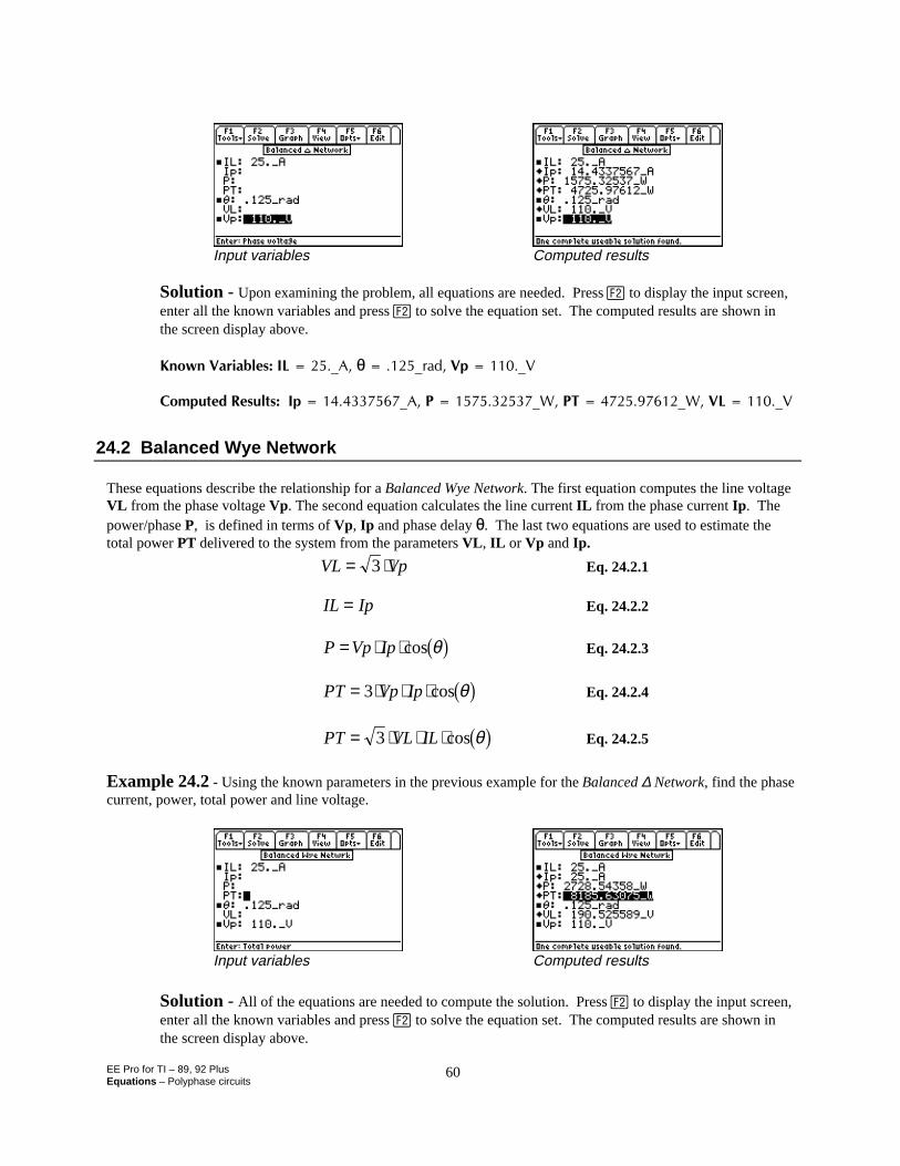
EE Pro for TI – 89, 92 PlusEquations – Polyphase circuits
60
Input variables Computed results
Solution - Upon examining the problem, all equations are needed. Press „ to display the input screen, enter all the known variables and press „ to solve the equation set. The computed results are shown in the screen display above.
-PQYP8CTKCDNGU+.A#θATCF8RA8
%QORWVGF4GUWNVU+RA#2A926A98.A8
24.2 Balanced Wye Network
These equations describe the relationship for a Balanced Wye Network. The first equation computes the line voltageVL from the phase voltage Vp. The second equation calculates the line current IL from the phase current Ip . Thepower/phase P, is defined in terms of Vp, Ip and phase delay θ. The last two equations are used to estimate thetotal power PT delivered to the system from the parameters VL , IL or Vp and Ip.
VL Vp= ⋅3 Eq. 24.2.1
IL Ip= Eq. 24.2.2
P Vp Ip= ⋅ ⋅cosθb g Eq. 24.2.3
PT Vp Ip= ⋅ ⋅ ⋅3 cosθb g Eq. 24.2.4
PT VL IL= ⋅ ⋅ ⋅3 cosθb g Eq. 24.2.5
Example 24.2 - Using the known parameters in the previous example for the Balanced ∆ Network, find the phasecurrent, power, total power and line voltage.
Input variables Computed results
Solution - All of the equations are needed to compute the solution. Press „ to display the input screen, enter all the known variables and press „ to solve the equation set. The computed results are shown in the screen display above.
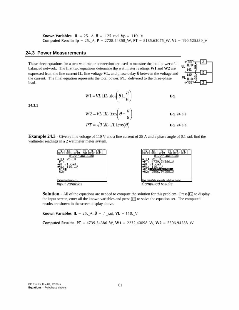
EE Pro for TI – 89, 92 PlusEquations – Polyphase circuits
61
-PQYP8CTKCDNGU+.A#θATCF8RA8%QORWVGF4GUWNVU+RA#2A926A98.A8
24.3 Power Measurements
These three equations for a two-watt meter connection are used to measure the total power of abalanced network. The first two equations determine the watt meter readings W1 and W2 areexpressed from the line current IL , line voltage VL , and phase delay θ between the voltage andthe current. The final equation represents the total power, PT, delivered to the three-phaseload.
W VL IL16
= ⋅ ⋅ +FHG
IKJcos θ π
Eq.
24.3.1
W VL IL26
= ⋅ ⋅ −FHG
IKJcos θ π
Eq. 24.3.2
PT VL IL= ⋅ ⋅ ⋅3 cosθb g Eq. 24.3.3
Example 24.3 - Given a line voltage of 110 V and a line current of 25 A and a phase angle of 0.1 rad, find thewattmeter readings in a 2 wattmeter meter system.
Input variables Computed results
Solution - All of the equations are needed to compute the solution for this problem. Press „ to display the input screen, enter all the known variables and press „ to solve the equation set. The computed results are shown in the screen display above.
-PQYP8CTKCDNGU+.A#θATCF8.A8
%QORWVGF4GUWNVU26A99A99A9
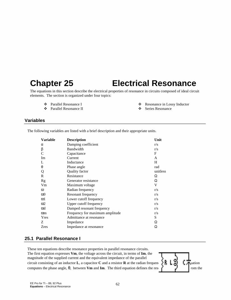
EE Pro for TI – 89, 92 PlusEquations – Electrical Resonance
62
Chapter 25 Electrical ResonanceThe equations in this section describe the electrical properties of resonance in circuits composed of ideal circuitelements. The section is organized under four topics:
Parallel Resonance IParallel Resonance II
Resonance in Lossy InductorSeries Resonance
Variables
The following variables are listed with a brief description and their appropriate units.
Variable Description Unitα Damping coefficient r/sβ Bandwidth r/sC Capacitance FIm Current AL Inductance Hθ Phase angle radQ Quality factor unitlessR Resistance ΩRg Generator resistance ΩVm Maximum voltage Vω Radian frequency r/sω0 Resonant frequency r/s ω1 Lower cutoff frequency r/sω2 Upper cutoff frequency r/sωd Damped resonant frequency r/sωm Frequency for maximum amplitude r/sYres Admittance at resonance SZ Impedance ΩZres Impedance at resonance Ω
25.1 Parallel Resonance I
These ten equations describe resonance properties in parallel resonance circuits.The first equation expresses Vm, the voltage across the circuit, in terms of Im , themagnitude of the supplied current and the equivalent impedance of the parallelcircuit consisting of an inductor L , a capacitor C and a resistor R at the radian frequency ω. The second equationcomputes the phase angle, θ, between Vm and Im . The third equation defines the resonant frequency ω0 from the
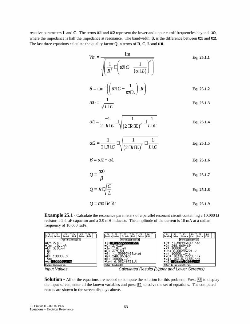
EE Pro for TI – 89, 92 PlusEquations – Electrical Resonance
63
reactive parameters L and C. The terms ω1 and ω2 represent the lower and upper cutoff frequencies beyond ω0,where the impedance is half the impedance at resonance. The bandwidth, β, is the difference between ω1 and ω2.The last three equations calculate the quality factor Q in terms of R, C, L and ω0.
Vm
RC
L
=
+ ⋅ −⋅
FHG
IKJ
FHGG
IKJJ
Im
1 12
2
ωωb g
Eq. 25.1.1
θ ωω
= ⋅ −⋅
FHG
IKJ ⋅F
HGIKJ
−tan 1 1C
LR Eq. 25.1.2
ω01=⋅L C
Eq. 25.1.3
ω11
2
1
2
12= −
⋅ ⋅+
⋅ ⋅+
⋅R C R C L Cb gEq. 25.1.4
ω21
2
1
2
12=
⋅ ⋅+
⋅ ⋅+
⋅R C R C L Cb gEq. 25.1.5
β ω ω= −2 1 Eq. 25.1.6
Q = ωβ0
Eq. 25.1.7
Q RC
L= ⋅ Eq. 25.1.8
Q R C= ⋅ ⋅ω0 Eq. 25.1.9
Example 25.1 - Calculate the resonance parameters of a parallel resonant circuit containing a 10,000 Ωresistor, a 2.4 µF capacitor and a 3.9 mH inductor. The amplitude of the current is 10 mA at a radianfrequency of 10,000 rad/s.
Input Values Calculated Results (Upper and Lower Screens)
Solution - All of the equations are needed to compute the solution for this problem. Press „ to displaythe input screen, enter all the known variables and press „ to solve the set of equations. The computedresults are shown in the screen displays above.
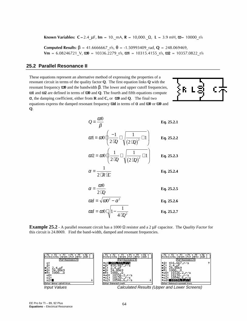
EE Pro for TI – 89, 92 PlusEquations – Electrical Resonance
64
-PQYP8CTKCDNGU%Aµ(+OAO#4AΩ.O*ωATU
%QORWVGF4GUWNVUβATUθATCF3
8OA8ωATUωATUωATU
25.2 Parallel Resonance II
These equations represent an alternative method of expressing the properties of aresonant circuit in terms of the quality factor Q. The first equation links Q with theresonant frequency ω0 and the bandwidth β. The lower and upper cutoff frequencies,ω1 and ω2 are defined in terms of ω0 and Q. The fourth and fifth equations computeα, the damping coefficient, either from R and C, or ω0 and Q. The final twoequations express the damped resonant frequency ωd in terms of α and ω0 or ω0 andQ.
Q = ωβ0
Eq. 25.2.1
ω ω1 01
2
1
212= ⋅ −
⋅+
⋅+
FHG
IKJQ Qb g
Eq. 25.2.2
ω ω2 01
2
1
212= ⋅
⋅+
⋅+
FHG
IKJQ Qb g
Eq. 25.2.3
α =⋅ ⋅
1
2 R CEq. 25.2.4
α ω=⋅0
2 QEq. 25.2.5
ω ω αd = −02 2 Eq. 25.2.6
ω ωdQ
= ⋅ −⋅
0 11
4 2Eq. 25.2.7
Example 25.2 - A parallel resonant circuit has a 1000 Ω resistor and a 2 µF capacitor. The Quality Factor forthis circuit is 24.8069. Find the band-width, damped and resonant frequencies.
Input Values Calculated Results (Upper and Lower Screens)
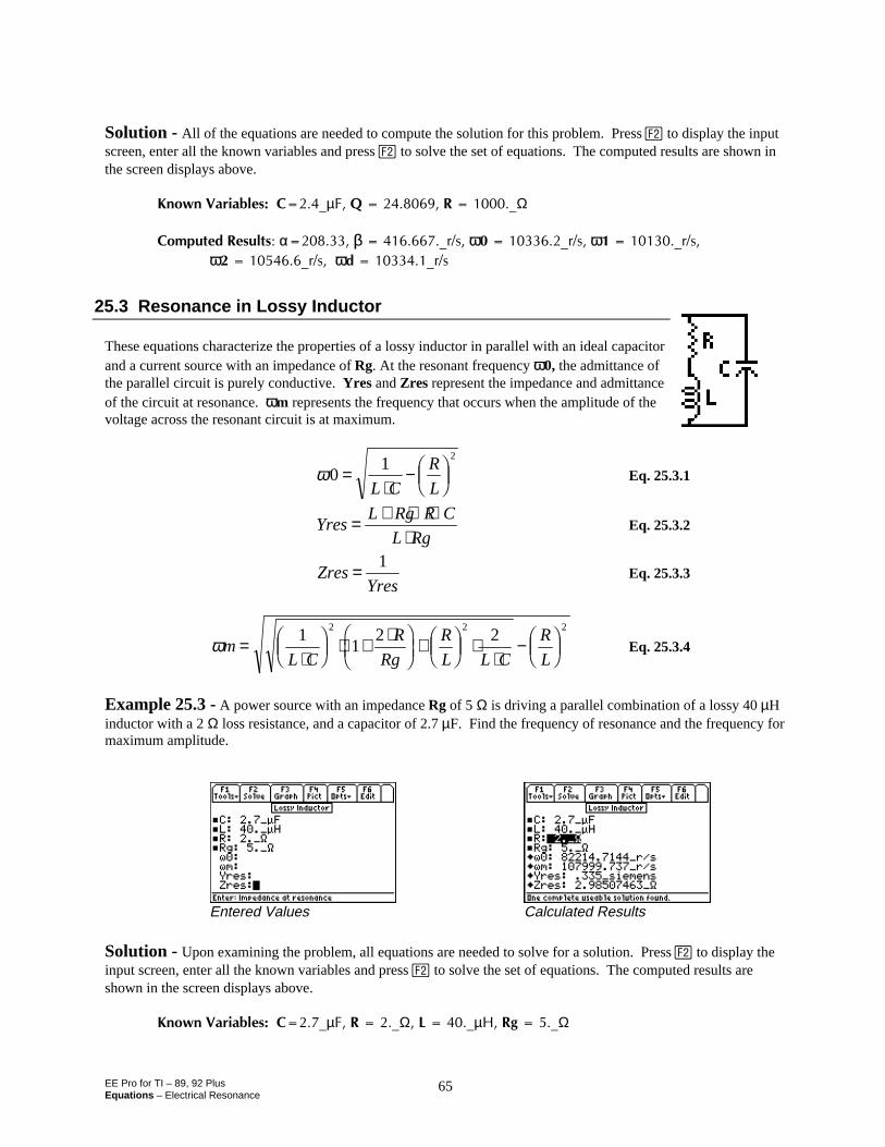
EE Pro for TI – 89, 92 PlusEquations – Electrical Resonance
65
Solution - All of the equations are needed to compute the solution for this problem. Press „ to display the inputscreen, enter all the known variables and press „ to solve the set of equations. The computed results are shown inthe screen displays above.
-PQYP8CTKCDNGU%Aµ(34AΩ
%QORWVGF4GUWNVUαββATUωωATUωωATU
ωωATUωωFATU
25.3 Resonance in Lossy Inductor
These equations characterize the properties of a lossy inductor in parallel with an ideal capacitorand a current source with an impedance of Rg. At the resonant frequency ωω0, the admittance ofthe parallel circuit is purely conductive. Yres and Zres represent the impedance and admittanceof the circuit at resonance. ωωm represents the frequency that occurs when the amplitude of thevoltage across the resonant circuit is at maximum.
ω01
2
=⋅
− FHG
IKJL C
R
LEq. 25.3.1
YresL Rg R C
L Rg= + ⋅ ⋅
⋅Eq. 25.3.2
ZresYres
= 1Eq. 25.3.3
ωmL C
R
Rg
R
L L C
R
L=
⋅FHG
IKJ ⋅ + ⋅F
HGIKJ + F
HGIKJ ⋅
⋅− FHG
IKJ
11
2 22 2 2
Eq. 25.3.4
Example 25.3 - A power source with an impedance Rg of 5 Ω is driving a parallel combination of a lossy 40 µHinductor with a 2 Ω loss resistance, and a capacitor of 2.7 µF. Find the frequency of resonance and the frequency formaximum amplitude.
Entered Values Calculated Results
Solution - Upon examining the problem, all equations are needed to solve for a solution. Press „ to display theinput screen, enter all the known variables and press „ to solve the set of equations. The computed results areshown in the screen displays above.
-PQYP8CTKCDNGU%Aµ(4AΩ.Aµ*4IAΩ
EE Pro for TI – 89, 92 PlusEquations – Electrical Resonance
66
%QORWVGF4GUWNVUωATUωOATU;TGUAUKGOGPU
<TGUAΩ
25.4 Series Resonance
These equations characterize the properties of a series resonance circuit. The first equationconnects the resonant frequency ωω0 and the reactive elements, the inductance L, and thecapacitance, C. The second and third equations compute the magnitude Z and phase θθ ofthe impedance, respectively.. The equations for ωω1 and ωω2 represent the upper and lowercutoff frequencies beyond resonance, where the impedance is half the impedance atresonance. The expressions for ββ represents the bandwidth of the resonant circuit.The last equation determines the quality factor Q in terms of R, C, L , and ωω0.
ω01=⋅L C
Eq. 25.4.1
Z R LC
= + ⋅ −⋅
FHG
IKJ
22
1ωω
Eq. 25.4.2
θω
ω=⋅ −
⋅F
H
GGG
I
K
JJJ
−tan 1
1L
CR
Eq. 25.4.3
ω12 2
12
= −⋅
+⋅
FHG
IKJ +
⋅R
L
R
L L CEq. 25.4.4
ω22 2
12
=⋅
+⋅
FHG
IKJ +
⋅R
L
R
L L CEq. 25.4.5
β ω ω= −2 1 Eq. 25.4.6
β = R
LEq. 25.4.7
QL
R= ⋅ω0
Eq. 25.4.8
QR
L
C= ⋅1
Eq. 25.4.9
Example 25.4 - Find the characteristic parameters of a series-resonant circuit with R = 25Ω, L = 69 µH,C = 0.01 µF and a radian frequency of 125,000 rad/s.

EE Pro for TI – 89, 92 PlusEquations – Electrical Resonance
67
Entered Values Calculated Results (Upper and Lower Screens)
Solution - Upon examining the problem, all equations are needed to solve the problem. Press „ to display theinput screen, enter all the known variables and press „ to solve the set of equations. The computed results areshown in the screen displays above.
-PQYP8CTKCDNGU%Aµ(4AΩ.Aµ*4AΩωωATU
%QORWVGF4GUWNVUωωATUωωATUωωATU
<AΩ
EE Pro for TI - 89, 92 PlusEquations - OpAmp Circuits
68
Chapter 26 OpAmp CircuitsSeven commonly-used OpAmp circuits are presented in this section. An OpAmp is a direct-coupled high-gainamplifier that can be configured with the use of feedback to circuit elements to achieve overall performancecharacteristics. There are two inputs labeled ‘+’ and ‘-’. The manner in which input signals are connected to theseterminals defines the inverting or non-inverting properties of the circuit.
Basic InverterNon-Inverting AmplifierCurrent AmplifierTransconductance Amplifier
Level Detector (Inverting)Level Detector (Non-Inverting)DifferentiatorDifferential Amplifier
Variables
All the variables used here are listed with a brief description and proper units.
Variable Description UnitAcc Common Mode current gain unitlessAco Common Mode gain from real OpAmp unitlessAd Differential mode gain unitlessAgc Transconductance SAic Current gain unitlessAv Voltage gain unitlessCC1 Input capacitor FCf Feedback capacitor FCMRR CM rejection ratio unitlessCp Bypass capacitor Ffcp 3dB bandwidth, circuit Hzfd Characteristic frequency Hzf0 Passband, geometric center Hzfop 3dB bandwidth, OpAmp HzIIf Maximum current through Rf ARR1 Input resistor ΩRR2 Current stabilizor ΩRR3 Feedback resistor ΩRR4 Resistor ΩRf Feedback resistor ΩRin Input resistance ΩRl Load resistance ΩRo Output resistance, OpAmp ΩRout Output resistance ΩRp Bias current resistor Ω
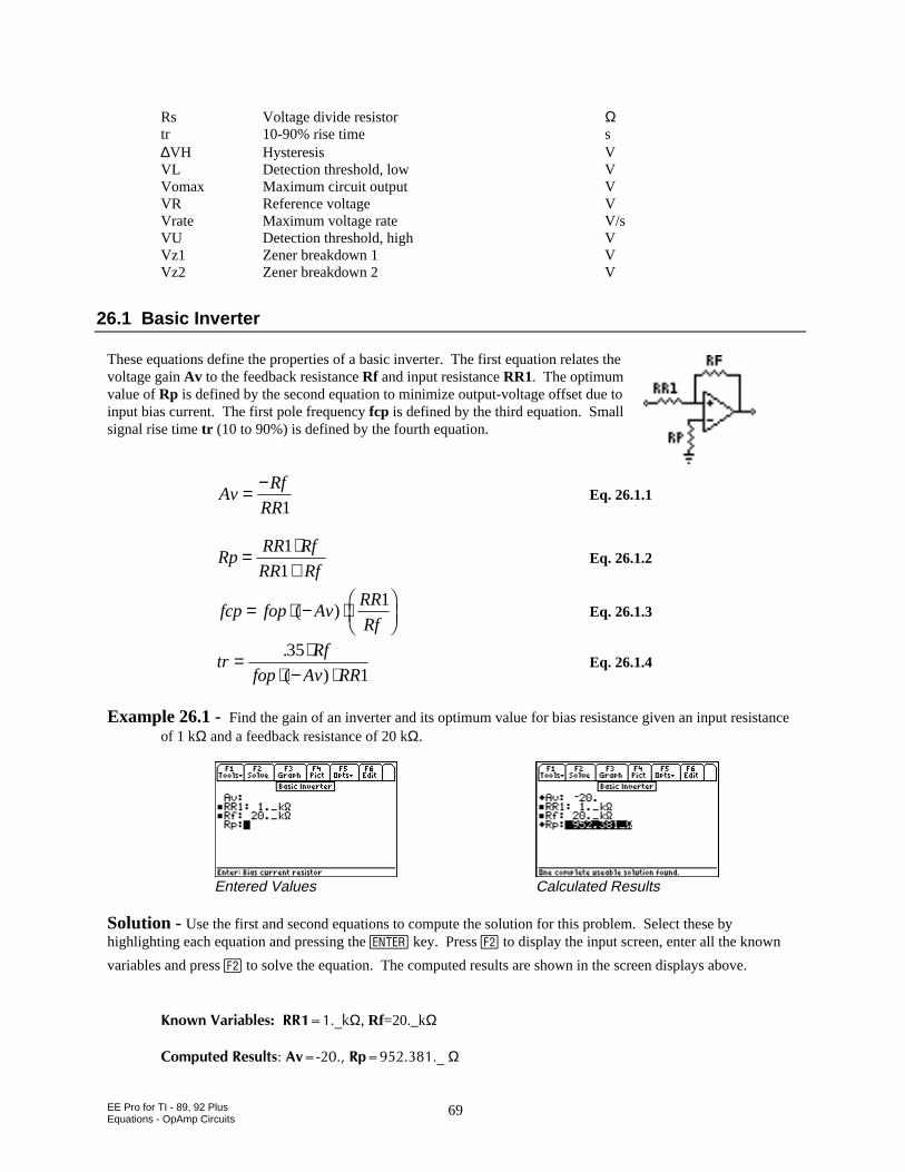
EE Pro for TI - 89, 92 PlusEquations - OpAmp Circuits
69
Rs Voltage divide resistor Ωtr 10-90% rise time s∆VH Hysteresis VVL Detection threshold, low VVomax Maximum circuit output VVR Reference voltage VVrate Maximum voltage rate V/sVU Detection threshold, high VVz1 Zener breakdown 1 VVz2 Zener breakdown 2 V
26.1 Basic Inverter
These equations define the properties of a basic inverter. The first equation relates thevoltage gain Av to the feedback resistance Rf and input resistance RR1. The optimumvalue of Rp is defined by the second equation to minimize output-voltage offset due toinput bias current. The first pole frequency fcp is defined by the third equation. Smallsignal rise time tr (10 to 90%) is defined by the fourth equation.
AvRf
RR= −
1Eq. 26.1.1
RpRR Rf
RR Rf= ⋅
+1
1Eq. 26.1.2
fcp fop AvRR
Rf= ⋅ − ⋅
FHG
IKJ( )
1Eq. 26.1.3
trRf
fop Av RR= ⋅
⋅ − ⋅.
( )
35
1Eq. 26.1.4
Example 26.1 - Find the gain of an inverter and its optimum value for bias resistance given an input resistanceof 1 kΩ and a feedback resistance of 20 kΩ.
Entered Values Calculated Results
Solution - Use the first and second equations to compute the solution for this problem. Select these byhighlighting each equation and pressing the key. Press „ to display the input screen, enter all the known
variables and press „ to solve the equation. The computed results are shown in the screen displays above.
-PQYP8CTKCDNGU44AMΩ, Rf=20._kΩ
%QORWVGF4GUWNVU#X4RA Ω
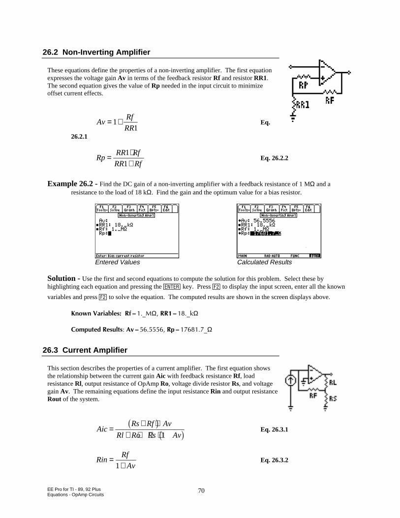
EE Pro for TI - 89, 92 PlusEquations - OpAmp Circuits
70
26.2 Non-Inverting Amplifier
These equations define the properties of a non-inverting amplifier. The first equationexpresses the voltage gain Av in terms of the feedback resistor Rf and resistor RR1.The second equation gives the value of Rp needed in the input circuit to minimizeoffset current effects.
AvRf
RR= +1
1Eq.
26.2.1
RpRR Rf
RR Rf= ⋅
+1
1Eq. 26.2.2
Example 26.2 - Find the DC gain of a non-inverting amplifier with a feedback resistance of 1 MΩ and aresistance to the load of 18 kΩ. Find the gain and the optimum value for a bias resistor.
Entered Values Calculated Results
Solution - Use the first and second equations to compute the solution for this problem. Select these byhighlighting each equation and pressing the key. Press „ to display the input screen, enter all the known
variables and press „ to solve the equation. The computed results are shown in the screen displays above.
-PQYP8CTKCDNGU4HA/Ω44AMΩ
%QORWVGF4GUWNVU#X4RAΩ
26.3 Current Amplifier
This section describes the properties of a current amplifier. The first equation showsthe relationship between the current gain Aic with feedback resistance Rf, loadresistance Rl, output resistance of OpAmp Ro, voltage divide resistor Rs, and voltagegain Av. The remaining equations define the input resistance Rin and output resistanceRout of the system.
AicRs Rf Av
Rl Ro Rs Av=
+ ⋅+ + ⋅ +b g
b g1Eq. 26.3.1
RinRf
Av=
+1Eq. 26.3.2
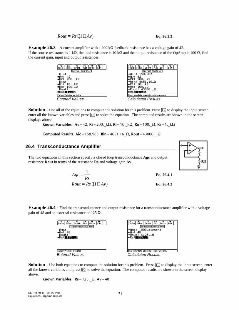
EE Pro for TI - 89, 92 PlusEquations - OpAmp Circuits
71
Rout Rs Av= ⋅ +1b g Eq. 26.3.3
Example 26.3 - A current amplifier with a 200 kΩ feedback resistance has a voltage gain of 42.If the source resistance is 1 kΩ, the load resistance is 10 kΩ and the output resistance of the OpAmp is 100 Ω, findthe current gain, input and output resistances.
Entered Values Calculated Results
Solution - Use all of the equations to compute the solution for this problem. Press „ to display the input screen,enter all the known variables and press „ to solve the equation. The computed results are shown in the screendisplays above.
-PQYP8CTKCDNGU#X4HAMΩ4NAMΩ4QAΩ4UAMΩ
%QORWVGF4GUWNVU#KE4KPAΩ4QWVAΩ
26.4 Transconductance Amplifier
The two equations in this section specify a closed loop transconductance Agc and outputresistance Rout in terms of the resistance Rs and voltage gain Av.
AgcRs
= 1Eq. 26.4.1
Rout Rs Av= ⋅ +1b g Eq. 26.4.2
Example 26.4 - Find the transconductance and output resistance for a transconductance amplifier with a voltagegain of 48 and an external resistance of 125 Ω
Entered Values Calculated Results
Solution - Use both equations to compute the solution for this problem. Press „ to display the input screen, enterall the known variables and press „ to solve the equation. The computed results are shown in the screen displayabove.
-PQYP8CTKCDNGU4UAΩ#X
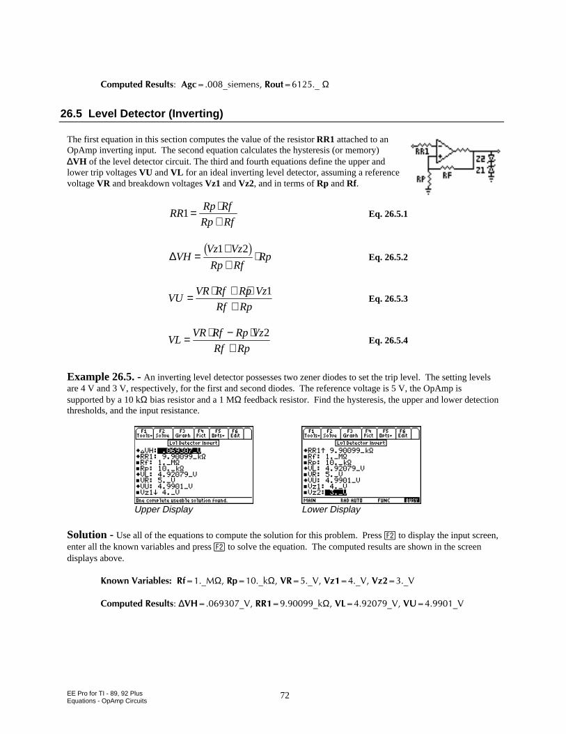
EE Pro for TI - 89, 92 PlusEquations - OpAmp Circuits
72
%QORWVGF4GUWNVU#IEAUKGOGPU4QWVAΩ
26.5 Level Detector (Inverting)
The first equation in this section computes the value of the resistor RR1 attached to anOpAmp inverting input. The second equation calculates the hysteresis (or memory)∆VH of the level detector circuit. The third and fourth equations define the upper andlower trip voltages VU and VL for an ideal inverting level detector, assuming a referencevoltage VR and breakdown voltages Vz1 and Vz2, and in terms of Rp and Rf.
RRRp Rf
Rp Rf1= ⋅
+Eq. 26.5.1
∆VHVz Vz
Rp RfRp=
++
⋅1 2b g
Eq. 26.5.2
VUVR Rf Rp Vz
Rf Rp= ⋅ + ⋅
+1
Eq. 26.5.3
VLVR Rf Rp Vz
Rf Rp= ⋅ − ⋅
+2
Eq. 26.5.4
Example 26.5. - An inverting level detector possesses two zener diodes to set the trip level. The setting levelsare 4 V and 3 V, respectively, for the first and second diodes. The reference voltage is 5 V, the OpAmp issupported by a 10 kΩbias resistor and a 1 MΩ feedback resistor. Find the hysteresis, the upper and lower detectionthresholds, and the input resistance.
Upper Display Lower Display
Solution - Use all of the equations to compute the solution for this problem. Press „ to display the input screen,enter all the known variables and press „ to solve the equation. The computed results are shown in the screendisplays above.
-PQYP8CTKCDNGU4HA/Ω4RAMΩ84A88\A88\A8
%QORWVGF4GUWNVU∆8*A844AMΩ8.A887A8
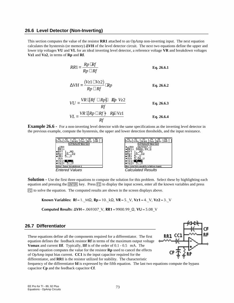
EE Pro for TI - 89, 92 PlusEquations - OpAmp Circuits
73
26.6 Level Detector (Non-Inverting)
This section computes the value of the resistor RR1 attached to an OpAmp non-inverting input. The next equationcalculates the hysteresis (or memory) ∆VH of the level detector circuit. The next two equations define the upper andlower trip voltages VU and VL for an ideal inverting level detector, a reference voltage VR and breakdown voltagesVz1 and Vz2, in terms of Rp and Rf.
RRRp Rf
Rp Rf1= ⋅
+Eq. 26.6.1
∆VHVz Vz
Rp RfRp=
++
⋅1 2b g
Eq. 26.6.2
VUVR Rf Rp Rp Vz
Rf=
⋅ + + ⋅b g 2Eq. 26.6.3
VLVR Rp Rf Rp Vz
Rf=
⋅ + − ⋅b g 1Eq. 26.6.4
Example 26.6 - For a non-inverting level detector with the same specifications as the inverting level detector inthe previous example, compute the hysteresis, the upper and lower detection thresholds, and the input resistance.
Entered Values Calculated Results
Solution - Use the first three equations to compute the solution for this problem. Select these by highlighting eachequation and pressing the key. Press „ to display the input screen, enter all the known variables and press
„ to solve the equation. The computed results are shown in the screen displays above.
-PQYP8CTKCDNGU4HA/Ω4RAMΩ84A88\A88\A8
%QORWVGF4GUWNVU∆8*A844AΩ87A8
26.7 Differentiator
These equations define all the components required for a differentiator. The firstequation defines the feedback resistor Rf in terms of the maximum output voltageVomax and current IIf . Typically, IIf is of the order of 0.1 - 0.5 mA. Thesecond equation computes the value for the resistor Rp used to cancel the effectsof OpAmp input bias current. CC1 is the input capacitor required for thedifferentiator, and RR1 is the resistor utilized for stability. The characteristicfrequency of the differentiator fd is expressed by the fifth equation. The last two equations compute the bypasscapacitor Cp and the feedback capacitor Cf.
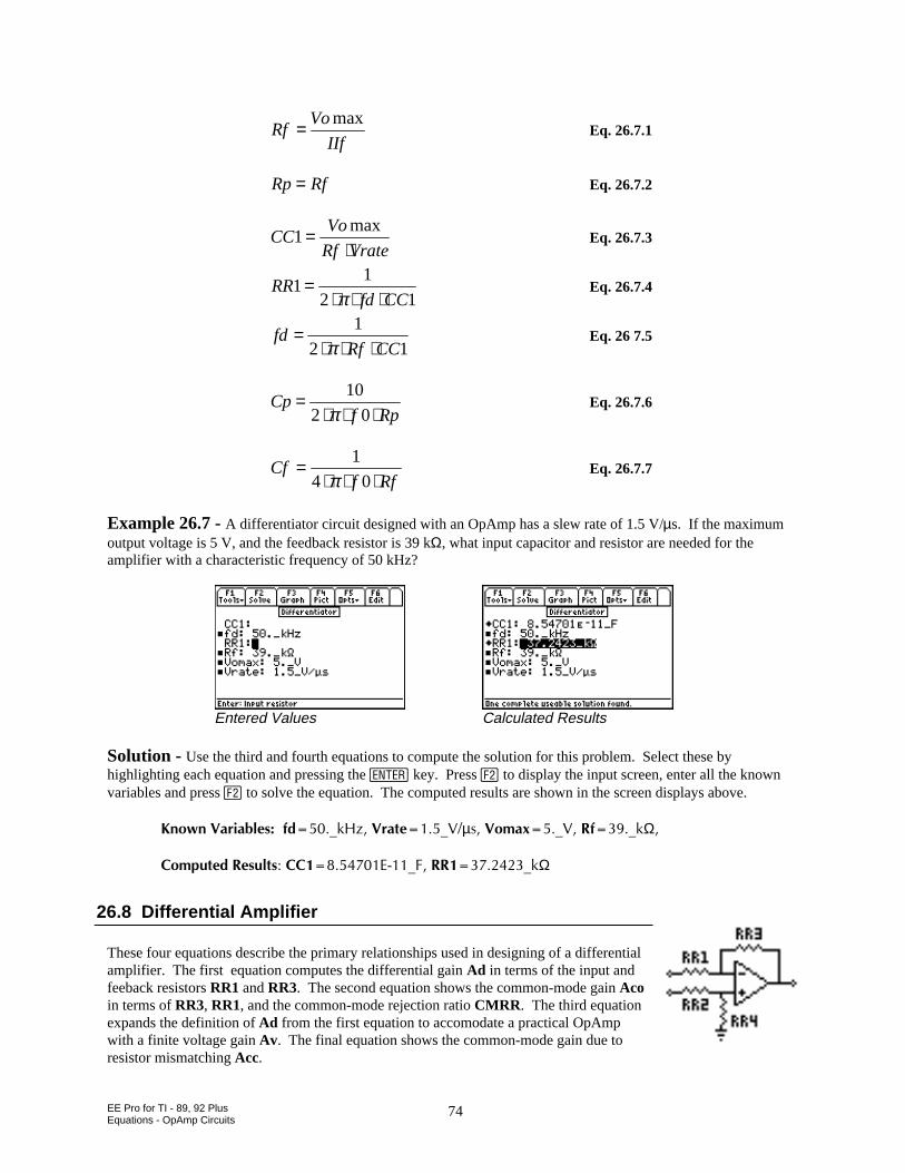
EE Pro for TI - 89, 92 PlusEquations - OpAmp Circuits
74
RfVo
IIf= max
Eq. 26.7.1
Rp Rf= Eq. 26.7.2
CCVo
Rf Vrate1=
⋅max
Eq. 26.7.3
RRfd CC
11
2 1=
⋅ ⋅ ⋅πEq. 26.7.4
fdRf CC
=⋅ ⋅ ⋅
1
2 1πEq. 26 7.5
Cpf Rp
=⋅ ⋅ ⋅
10
2 0πEq. 26.7.6
Cff Rf
=⋅ ⋅ ⋅
1
4 0πEq. 26.7.7
Example 26.7 - A differentiator circuit designed with an OpAmp has a slew rate of 1.5 V/µs. If the maximumoutput voltage is 5 V, and the feedback resistor is 39 kΩ, what input capacitor and resistor are needed for theamplifier with a characteristic frequency of 50 kHz?
Entered Values Calculated Results
Solution - Use the third and fourth equations to compute the solution for this problem. Select these byhighlighting each equation and pressing the key. Press „ to display the input screen, enter all the knownvariables and press „ to solve the equation. The computed results are shown in the screen displays above.
-PQYP8CTKCDNGUHFAM*\8TCVGA8µU8QOCZA84HAMΩ
%QORWVGF4GUWNVU%%'A(44AMΩ
26.8 Differential Amplifier
These four equations describe the primary relationships used in designing of a differentialamplifier. The first equation computes the differential gain Ad in terms of the input andfeeback resistors RR1 and RR3. The second equation shows the common-mode gain Acoin terms of RR3, RR1, and the common-mode rejection ratio CMRR . The third equationexpands the definition of Ad from the first equation to accomodate a practical OpAmpwith a finite voltage gain Av. The final equation shows the common-mode gain due toresistor mismatching Acc.
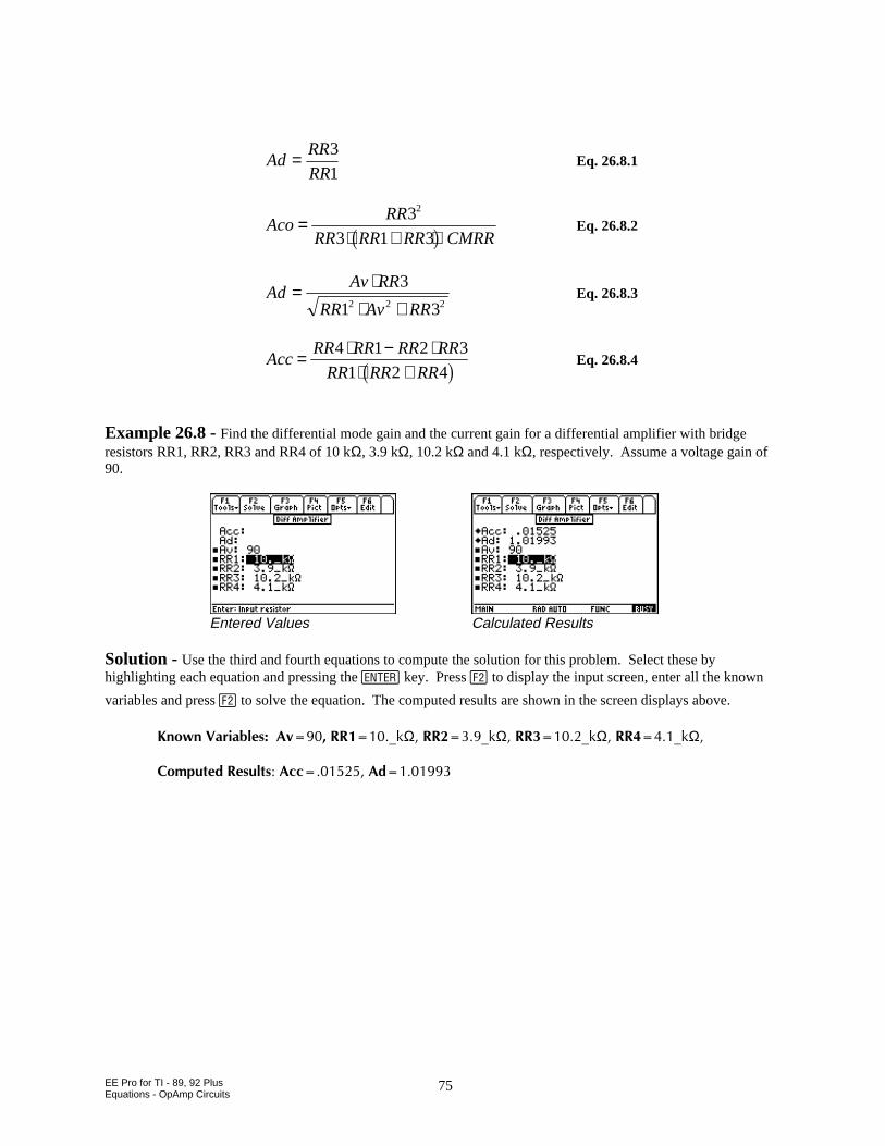
EE Pro for TI - 89, 92 PlusEquations - OpAmp Circuits
75
AdRR
RR= 3
1Eq. 26.8.1
AcoRR
RR RR RR CMRR=
⋅ + ⋅3
3 1 3
2
b g Eq. 26.8.2
AdAv RR
RR Av RR= ⋅
⋅ +3
1 32 2 2Eq. 26.8.3
AccRR RR RR RR
RR RR RR= ⋅ − ⋅
⋅ +4 1 2 3
1 2 4b g Eq. 26.8.4
Example 26.8 - Find the differential mode gain and the current gain for a differential amplifier with bridgeresistors RR1, RR2, RR3 and RR4 of 10 kΩ, 3.9 kΩ, 10.2 kΩ and 4.1 kΩ, respectively. Assume a voltage gain of90.
Entered Values Calculated Results
Solution - Use the third and fourth equations to compute the solution for this problem. Select these byhighlighting each equation and pressing the key. Press „ to display the input screen, enter all the known
variables and press „ to solve the equation. The computed results are shown in the screen displays above.
-PQYP8CTKCDNGU#X44AMΩ44AMΩ44AMΩ44AMΩ
%QORWVGF4GUWNVU#EE#F
EE PRO for TI-89, 92 PlusEquations - Solid State Devices
77
Chapter 27 Solid State DevicesThis section covers a variety of topics in solid state electronics.
Read this!Note: The equations in this section are grouped under topics which describe general properties of semiconductors ordevices. Equations for a variety of specific cases and are listed together under a sub-topic heading and are notnecessarily a set of consistent equations which can be solved together. Choosing equations in a subtopic w/o regard asto whether the equations represent actual relationships could generate erroneous results or no solution at all. Read thedescription of each equation set to determine which equations in a sub-topic form a consistent subset before attemptingto compute a solution.
Semiconductor BasicsPN JunctionsPN Junction CurrentsTransistor CurrentsEbers-Moll EquationsIdeal Currents - pnpSwitching Transients
MOS Transistor IMOS Transistor IIMOS Inverter (Resistive)MOS Inverter (Saturated)MOS Inverter (Depletion)CMOS Transistor PairJunction FET
Variables
A complete list of all the variables used in this section along with a brief description and appropriate units is givenbelow.
Variable Description Unitα CB current gain unitless
aLGJ Linearly graded junction parameter 1/m4
A Area m2
A1 EB junction area m2
A2 CB junction area m2
αf Forward α unitless
Aj Junction area m2
αr Reverse α unitlessβ CE current gain unitlessb Channel width mβf Forward β unitlessβr Reverse β unitlessCj Junction capacitance F

EE PRO for TI-89, 92 PlusEquations - Solid State Devices
78
CL Load capacitance F
Cox Oxide capacitance per unit area F/m2
D Diffusion coefficient m2/s
DB Base diffusion coefficient m2/s
DC Collector diffusion coefficient m2/s
DE Emitter diffusion coefficient m2/s
Dn n diffusion coefficient m2/s
Dp p diffusion coefficient m2/sεox Oxide permittivity unitlessεs Silicon Permittivity unitlessEc Conduction band JEF Fermi level JEi Intrinsic Fermi level JEv Valence band Jffmax Maximum frequency Hz
γ Body coefficient V.5
gd Drain conductance Sgm Transconductance SgmL Transconductance, load device SGo Conductance SI Junction current AI0 Saturation current AIB Base current AIC Collector current AICB0 CB leakage, E open AICE0 CE leakage, B open AICsat Collector I at saturation edge AID Drain current AIDmod Channel modulation drain current AID0 Drain current at zero bias AIDsat Drain saturation current AIE Emitter current AIIf Forward current AIr Reverse current AIr0 E-M reverse current component AIRG G-R current AIRG0 Zero bias G-R current AIs Saturation current Aλ Modulation parameter 1/VIs Saturation current A
kD MOS constant, driver A/V2
kL MOS constant, load A/V2
kn MOS constant A/V2
kn1 MOS process constant A/V2
kN MOS constant, n channel A/V2
kP MOS constant, p channel A/V2
KR Ratio unitlessL Transistor length mLC Diffusion length, collector mLD Drive transistor length mLE Diffusion length, emitter mLL Load transistor length m

EE PRO for TI-89, 92 PlusEquations - Solid State Devices
79
LLn Diffusion length, n mlNN n-channel length mLp Diffusion length, p mlP p-channel length m
µn n (electron) mobility m2/(V*s)
µp p (positive charge) mobility m2/(V*s)mn n effective mass unitlessmp p effective mass unitless
N Doping concentration 1/m3
Na Acceptor density 1/m3
nnC n density, collector 1/m3
Nd Donor density 1/m3
nE n density, emitter 1/m3
ni Intrinsic density 1/m3
N0 Surface concentration 1/m3
npo n density in p material 1/m3
p p density 1/m3
pB p density, base 1/m3
φF Fermi potential VφGC Work function potential V
pno p density in n material 1/m3
Qtot Total surface impurities unitless
Qb Bulk charge at bias C/m2
Qb0 Bulk charge at 0 bias C/m2
Qox Oxide charge density C/m2
Qsat Base Q, transition edge Cρn n resistivity Ω*mρp p resistivity Ω*mRl Load resistance ΩτB lifetime in base sτD Time constant sτL Time constant sτo Lifetime sτp Minority carrier lifetime sτt Base transit time st Time sTT Temperature Ktch Charging time stdis Discharge time stox Gate oxide thickness mtr Collector current rise time sts Charge storage time stsd1 Storage delay, turn off stsd2 Storage delay, turn off sTtr Transit time sV1 Input voltage VVa Applied voltage VVbi Built-in voltage VVBE BE bias voltage VVCB CB bias voltage VVCC Collector supply voltage V
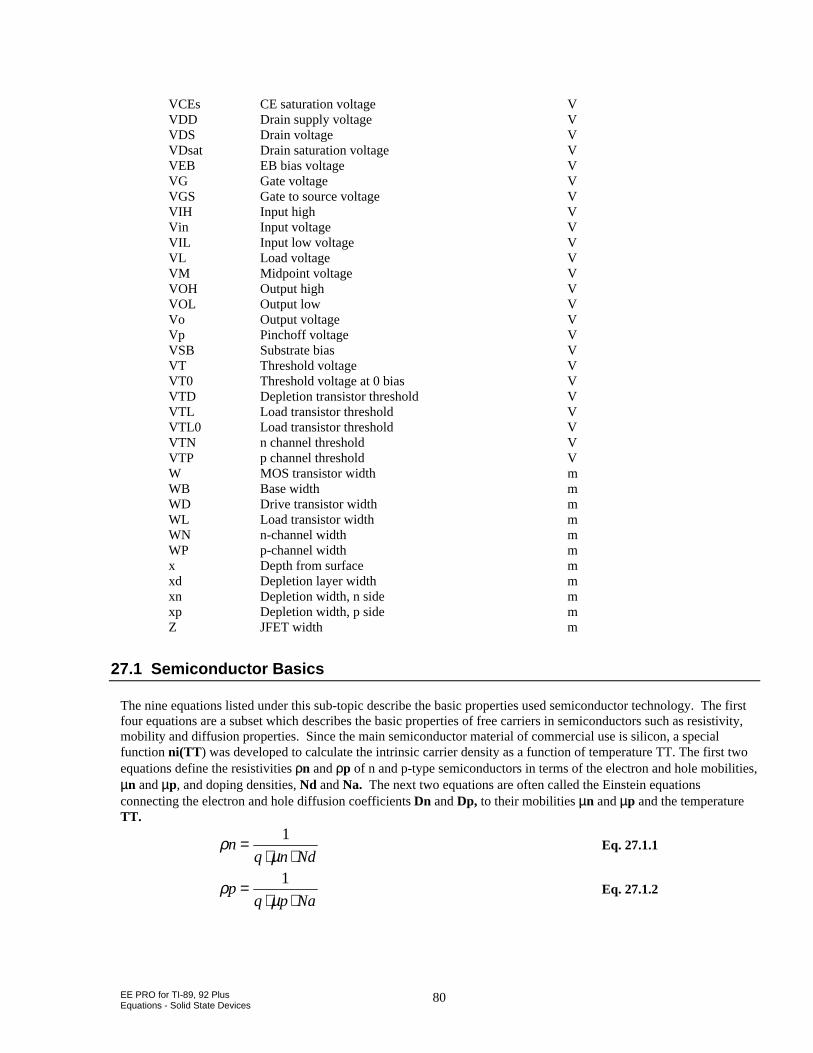
EE PRO for TI-89, 92 PlusEquations - Solid State Devices
80
VCEs CE saturation voltage VVDD Drain supply voltage VVDS Drain voltage VVDsat Drain saturation voltage VVEB EB bias voltage VVG Gate voltage VVGS Gate to source voltage VVIH Input high VVin Input voltage VVIL Input low voltage VVL Load voltage VVM Midpoint voltage VVOH Output high VVOL Output low VVo Output voltage VVp Pinchoff voltage VVSB Substrate bias VVT Threshold voltage VVT0 Threshold voltage at 0 bias VVTD Depletion transistor threshold VVTL Load transistor threshold VVTL0 Load transistor threshold VVTN n channel threshold VVTP p channel threshold VW MOS transistor width mWB Base width mWD Drive transistor width mWL Load transistor width mWN n-channel width mWP p-channel width mx Depth from surface mxd Depletion layer width mxn Depletion width, n side mxp Depletion width, p side mZ JFET width m
27.1 Semiconductor Basics
The nine equations listed under this sub-topic describe the basic properties used semiconductor technology. The firstfour equations are a subset which describes the basic properties of free carriers in semiconductors such as resistivity,mobility and diffusion properties. Since the main semiconductor material of commercial use is silicon, a specialfunction ni(TT ) was developed to calculate the intrinsic carrier density as a function of temperature TT. The first twoequations define the resistivities ρn and ρp of n and p-type semiconductors in terms of the electron and hole mobilities,µn and µp, and doping densities, Nd and Na. The next two equations are often called the Einstein equationsconnecting the electron and hole diffusion coefficients Dn and Dp, to their mobilities µn and µp and the temperatureTT.
ρµ
nq n Nd
=⋅ ⋅
1Eq. 27.1.1
ρµ
pq p Na
=⋅ ⋅
1Eq. 27.1.2
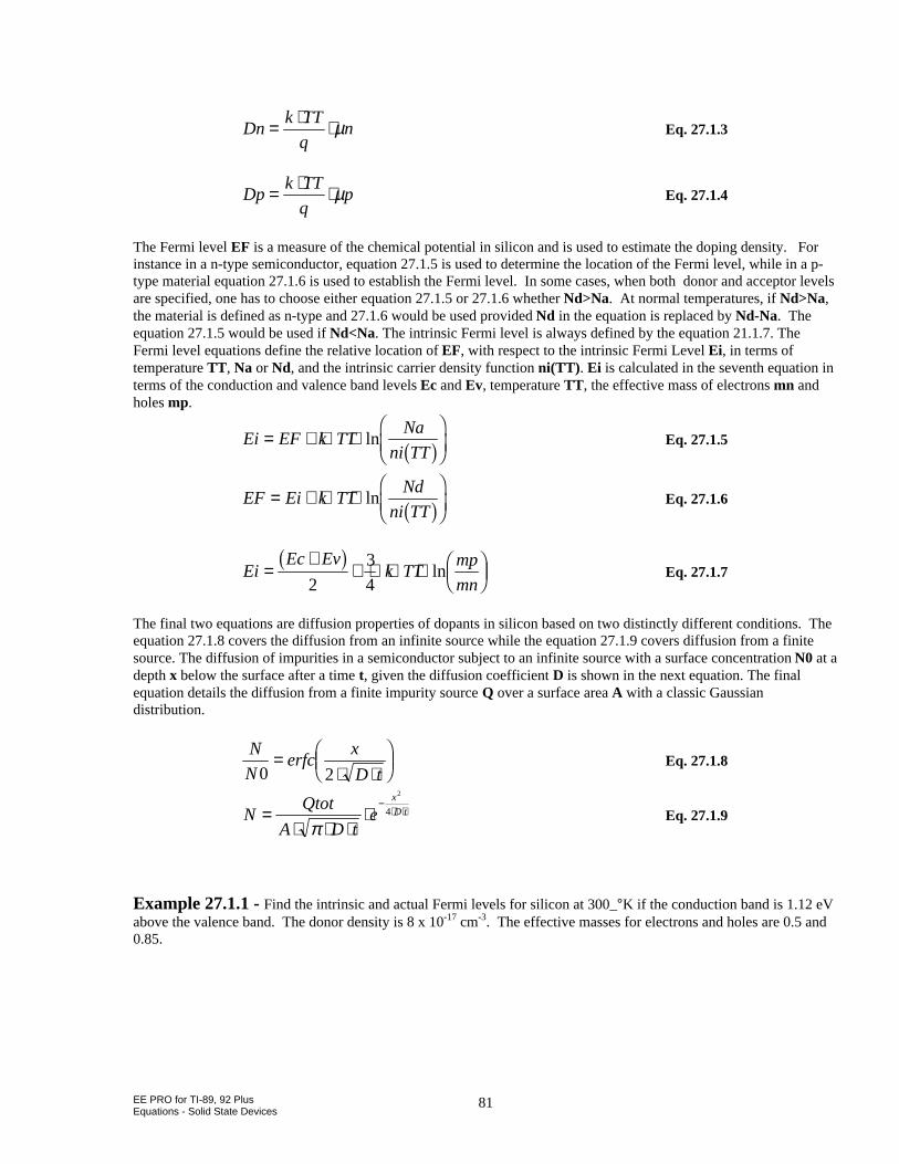
EE PRO for TI-89, 92 PlusEquations - Solid State Devices
81
Dnk TT
qn= ⋅ ⋅ µ Eq. 27.1.3
Dpk TT
qp= ⋅ ⋅ µ Eq. 27.1.4
The Fermi level EF is a measure of the chemical potential in silicon and is used to estimate the doping density. Forinstance in a n-type semiconductor, equation 27.1.5 is used to determine the location of the Fermi level, while in a p-type material equation 27.1.6 is used to establish the Fermi level. In some cases, when both donor and acceptor levelsare specified, one has to choose either equation 27.1.5 or 27.1.6 whether Nd>Na. At normal temperatures, if Nd>Na,the material is defined as n-type and 27.1.6 would be used provided Nd in the equation is replaced by Nd-Na. Theequation 27.1.5 would be used if Nd<Na. The intrinsic Fermi level is always defined by the equation 21.1.7. TheFermi level equations define the relative location of EF, with respect to the intrinsic Fermi Level Ei, in terms oftemperature TT , Na or Nd, and the intrinsic carrier density function ni(TT) . Ei is calculated in the seventh equation interms of the conduction and valence band levels Ec and Ev, temperature TT , the effective mass of electrons mn andholes mp.
Ei EF k TTNa
ni TT= + ⋅ ⋅
FHG
IKJln b g Eq. 27.1.5
EF Ei k TTNd
ni TT= + ⋅ ⋅
FHG
IKJln b g Eq. 27.1.6
EiEc Ev
k TTmp
mn=
++ ⋅ ⋅ ⋅ F
HGIKJ
b g2
3
4ln Eq. 27.1.7
The final two equations are diffusion properties of dopants in silicon based on two distinctly different conditions. Theequation 27.1.8 covers the diffusion from an infinite source while the equation 27.1.9 covers diffusion from a finitesource. The diffusion of impurities in a semiconductor subject to an infinite source with a surface concentration N0 at adepth x below the surface after a time t, given the diffusion coefficient D is shown in the next equation. The finalequation details the diffusion from a finite impurity source Q over a surface area A with a classic Gaussiandistribution.
N
Nerfc
x
D t0 2=
⋅ ⋅FHG
IKJ Eq. 27.1.8
NQtot
A D te
x
D t=⋅ ⋅ ⋅
⋅−
⋅ ⋅
π
2
4 Eq. 27.1.9
Example 27.1.1 - Find the intrinsic and actual Fermi levels for silicon at 300_°K if the conduction band is 1.12 eVabove the valence band. The donor density is 8 x 10-17 cm-3. The effective masses for electrons and holes are 0.5 and0.85.
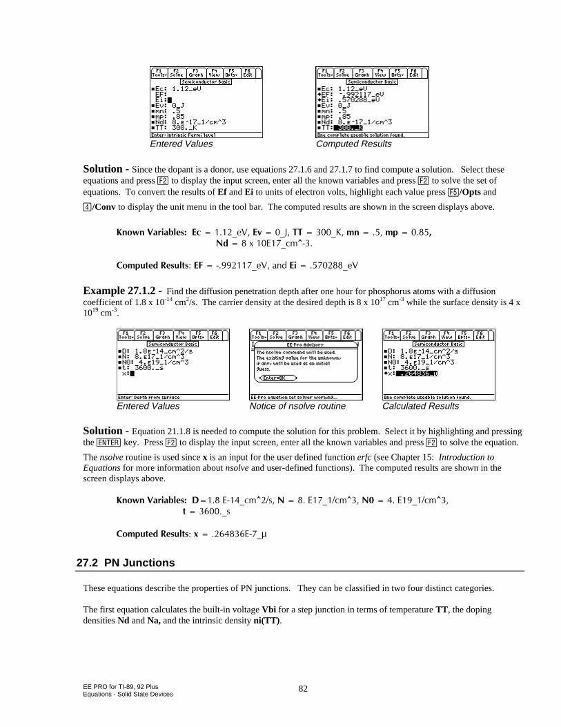
EE PRO for TI-89, 92 PlusEquations - Solid State Devices
82
Entered Values Computed Results
Solution - Since the dopant is a donor, use equations 27.1.6 and 27.1.7 to find compute a solution. Select theseequations and press „ to display the input screen, enter all the known variables and press „ to solve the set ofequations. To convert the results of Ef and Ei to units of electron volts, highlight each value press ‡/Opts and
y/Conv to display the unit menu in the tool bar. The computed results are shown in the screen displays above.
-PQYP8CTKCDNGU'EAG8'XA,66A-OPOR 0FZ'AEO@
%QORWVGF4GUWNVU'(AG8CPF'KAG8
Example 27.1.2 - Find the diffusion penetration depth after one hour for phosphorus atoms with a diffusioncoefficient of 1.8 x 10⁻¹⁴ cm2/s. The carrier density at the desired depth is 8 x 1017 cm-3 while the surface density is 4 x1019 cm-3.
Entered Values Notice of nsolve routine Calculated Results
Solution - Equation 21.1.8 is needed to compute the solution for this problem. Select it by highlighting and pressingthe key. Press „ to display the input screen, enter all the known variables and press „ to solve the equation.
The nsolve routine is used since x is an input for the user defined function erfc (see Chapter 15: Introduction toEquations for more information about nsolve and user-defined functions). The computed results are shown in thescreen displays above.
-PQYP8CTKCDNGU&'AEO@U0'AEO@0'AEO@VAU
%QORWVGF4GUWNVUZ'Aµ
27.2 PN Junctions
These equations describe the properties of PN junctions. They can be classified in two four distinct categories.
The first equation calculates the built-in voltage Vbi for a step junction in terms of temperature TT , the dopingdensities Nd and Na, and the intrinsic density ni(TT) .
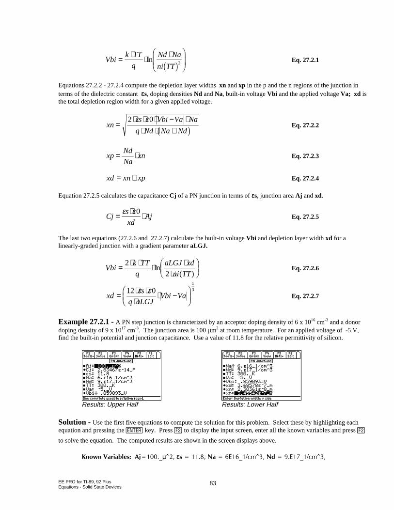
EE PRO for TI-89, 92 PlusEquations - Solid State Devices
83
Vbik TT
q
Nd Na
ni TT= ⋅ ⋅ ⋅F
HGIKJ
lnb g2 Eq. 27.2.1
Equations 27.2.2 - 27.2.4 compute the depletion layer widths xn and xp in the p and the n regions of the junction interms of the dielectric constant εεs, doping densities Nd and Na, built-in voltage Vbi and the applied voltage Va; xd isthe total depletion region width for a given applied voltage.
xns Vbi Va Na
q Nd Na Nd=
⋅ ⋅ ⋅ − ⋅⋅ ⋅ +
2 0ε εb g Eq. 27.2.2
xpNd
Naxn= ⋅ Eq. 27.2.3
xd xn xp= + Eq. 27.2.4 Equation 27.2.5 calculates the capacitance Cj of a PN junction in terms of εs, junction area Aj and xd.
Cjs
xdAj= ⋅ ⋅ε ε0
Eq. 27.2.5
The last two equations (27.2.6 and 27.2.7) calculate the built-in voltage Vbi and depletion layer width xd for alinearly-graded junction with a gradient parameter aLGJ.
Vbik TT
q
aLGJ xd
ni TT= ⋅ ⋅ ⋅ ⋅
⋅FHG
IKJ
2
2ln
( )Eq. 27.2.6
xds
q aLGJVbi Va= ⋅ ⋅
⋅⋅ −
FHG
IKJ
12 01
3ε εEq. 27.2.7
Example 27.2.1 - A PN step junction is characterized by an acceptor doping density of 6 x 1016 cm-3 and a donordoping density of 9 x 1017 cm-3. The junction area is 100 µm2 at room temperature. For an applied voltage of -5 V,find the built-in potential and junction capacitance. Use a value of 11.8 for the relative permittivity of silicon.
Results: Upper Half Results: Lower Half
Solution - Use the first five equations to compute the solution for this problem. Select these by highlighting eachequation and pressing the key. Press „ to display the input screen, enter all the known variables and press „
to solve the equation. The computed results are shown in the screen displays above.
-PQYP8CTKCDNGU#LAµ@εεU0C'AEO@0F'AEO@
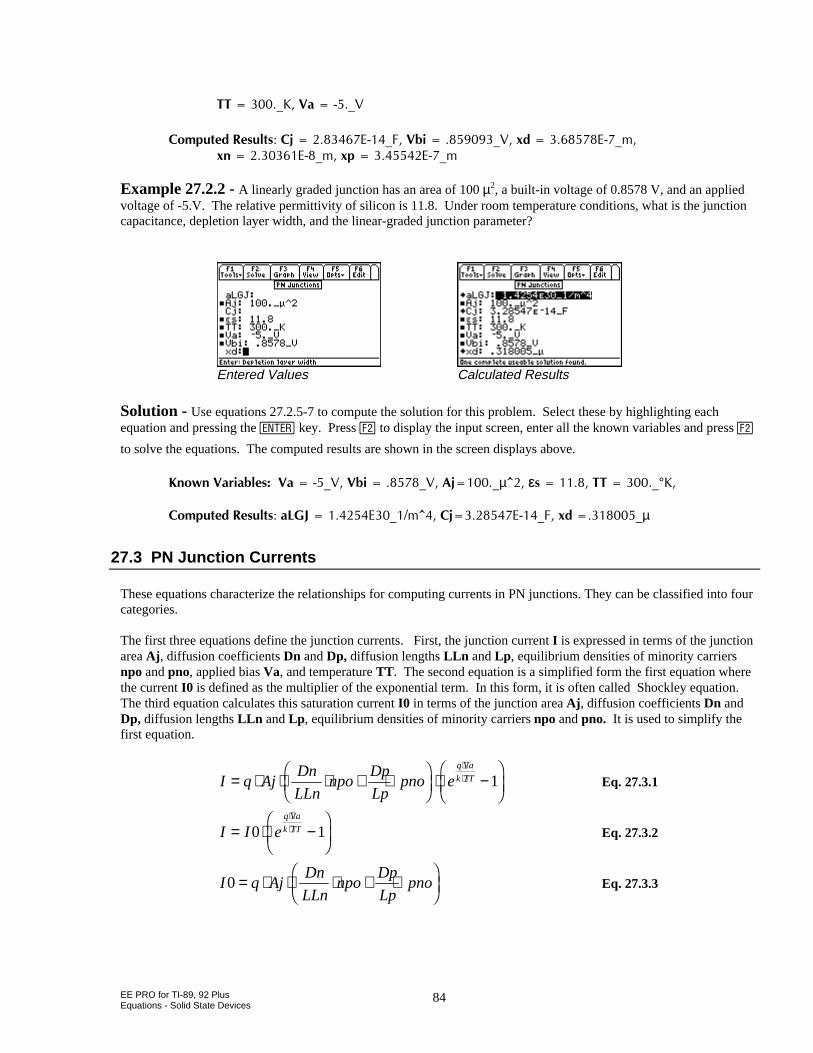
EE PRO for TI-89, 92 PlusEquations - Solid State Devices
84
66A-8CA8
%QORWVGF4GUWNVU%L'A(8DKA8ZF'AOZP'AOZR'AO
Example 27.2.2 - A linearly graded junction has an area of 100 µ2, a built-in voltage of 0.8578 V, and an appliedvoltage of -5.V. The relative permittivity of silicon is 11.8. Under room temperature conditions, what is the junctioncapacitance, depletion layer width, and the linear-graded junction parameter?
Entered Values Calculated Results
Solution - Use equations 27.2.5-7 to compute the solution for this problem. Select these by highlighting eachequation and pressing the key. Press „ to display the input screen, enter all the known variables and press „
to solve the equations. The computed results are shown in the screen displays above.
-PQYP8CTKCDNGU8CA88DKA8#LAµ@εεU66A°-
%QORWVGF4GUWNVUC.),'AO@%L'A(ZFAµ
27.3 PN Junction Currents
These equations characterize the relationships for computing currents in PN junctions. They can be classified into fourcategories.
The first three equations define the junction currents. First, the junction current I is expressed in terms of the junctionarea Aj , diffusion coefficients Dn and Dp, diffusion lengths LLn and Lp, equilibrium densities of minority carriersnpo and pno, applied bias Va, and temperature TT . The second equation is a simplified form the first equation wherethe current I0 is defined as the multiplier of the exponential term. In this form, it is often called Shockley equation.The third equation calculates this saturation current I0 in terms of the junction area Aj , diffusion coefficients Dn andDp, diffusion lengths LLn and Lp, equilibrium densities of minority carriers npo and pno. It is used to simplify thefirst equation.
I q AjDn
LLnnpo
Dp
Lppno e
q Va
k TT= ⋅ ⋅ ⋅ + ⋅FHG
IKJ ⋅ −FHG
IKJ
⋅⋅ 1 Eq. 27.3.1
I I eq Va
k TT= ⋅ −FHG
IKJ
⋅⋅0 1 Eq. 27.3.2
I q AjDn
LLnnpo
Dp
Lppno0 = ⋅ ⋅ ⋅ + ⋅
FHG
IKJ Eq. 27.3.3
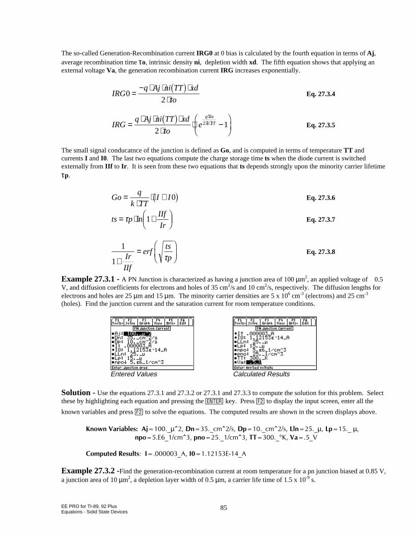
EE PRO for TI-89, 92 PlusEquations - Solid State Devices
85
The so-called Generation-Recombination current IRG0 at 0 bias is calculated by the fourth equation in terms of Aj ,average recombination time τo, intrinsic density ni, depletion width xd. The fifth equation shows that applying anexternal voltage Va, the generation recombination current IRG increases exponentially.
IRGq Aj ni TT xd
o0
2=
− ⋅ ⋅ ⋅⋅b g
τEq. 27.3.4
IRGq Aj ni TT xd
oe
q Va
k TT=⋅ ⋅ ⋅
⋅⋅ −FHG
IKJ
⋅⋅ ⋅b g
212
τEq. 27.3.5
The small signal conducatnce of the junction is defined as Go, and is computed in terms of temperature TT andcurrents I and I0. The last two equations compute the charge storage time ts when the diode current is switchedexternally from IIf to Ir . It is seen from these two equations that ts depends strongly upon the minority carrier lifetimeτp.
Goq
k TTI I=
⋅⋅ + 0b g Eq. 27.3.6
ts pIIf
Ir= ⋅ +F
HGIKJτ ln 1 Eq. 27.3.7
1
1+=
FHG
IKJIr
IIf
erfts
pτEq. 27.3.8
Example 27.3.1 - A PN Junction is characterized as having a junction area of 100 µm2, an applied voltage of 0.5V, and diffusion coefficients for electrons and holes of 35 cm2/s and 10 cm2/s, respectively. The diffusion lengths forelectrons and holes are 25 µm and 15 µm. The minority carrier densities are 5 x 106 cm-3 (electrons) and 25 cm-3
(holes). Find the junction current and the saturation current for room temperature conditions.
Entered Values Calculated Results
Solution - Use the equations 27.3.1 and 27.3.2 or 27.3.1 and 27.3.3 to compute the solution for this problem. Selectthese by highlighting each equation and pressing the key. Press „ to display the input screen, enter all the
known variables and press „ to solve the equations. The computed results are shown in the screen displays above.
-PQYP8CTKCDNGU#LAµ@&PAEO@U&[email protected]µ.RAµPRQ'AEO@RPQAEO@66A°-8CA8
%QORWVGF4GUWNVU+A#+'A#
Example 27.3.2 -Find the generation-recombination current at room temperature for a pn junction biased at 0.85 V,a junction area of 10 µm2, a depletion layer width of 0.5 µm, a carrier life time of 1.5 x 10⁻⁹ s.
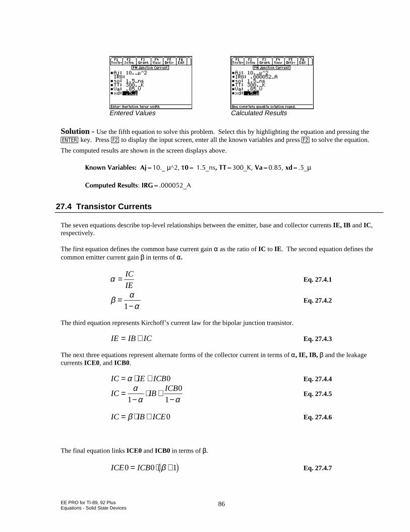
EE PRO for TI-89, 92 PlusEquations - Solid State Devices
86
Entered Values Calculated Results
Solution - Use the fifth equation to solve this problem. Select this by highlighting the equation and pressing the¸ key. Press „ to display the input screen, enter all the known variables and press „ to solve the equation.
The computed results are shown in the screen displays above.
-PQYP8CTKCDNGU#LA µ^ττAPU66A-8CZFAµ
%QORWVGF4GUWNVU+4)A#
27.4 Transistor Currents
The seven equations describe top-level relationships between the emitter, base and collector currents IE, IB and IC ,respectively.
The first equation defines the common base current gain α as the ratio of IC to IE . The second equation defines thecommon emitter current gain β in terms of α.
α = IC
IEEq. 27.4.1
β αα
=−1
Eq. 27.4.2
The third equation represents Kirchoff’s current law for the bipolar junction transistor.
IE IB IC= + Eq. 27.4.3
The next three equations represent alternate forms of the collector current in terms of α, IE, IB, β and the leakagecurrents ICE0, and ICB0.
IC IE ICB= ⋅ +α 0 Eq. 27.4.4
IC IBICB=
−⋅ +
−α
α α1
0
1Eq. 27.4.5
IC IB ICE= ⋅ +β 0 Eq. 27.4.6
The final equation links ICE0 and ICB0 in terms of β.
ICE ICB0 0 1= ⋅ +βb g Eq. 27.4.7
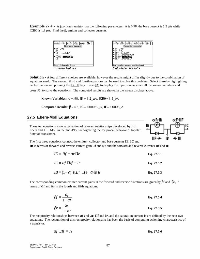
EE PRO for TI-89, 92 PlusEquations - Solid State Devices
87
Example 27.4 - A junction transistor has the following parameters: α is 0.98, the base current is 1.2 µA whileICBO is 1.8 pA. Find the β, emitter and collector currents.
Entered Values Calculated Results
Solution - A few different choices are available, however the results might differ slightly due to the combination ofequations used. The second, third and fourth equations can be used to solve this problem. Select these by highlightingeach equation and pressing the key. Press „ to display the input screen, enter all the known variables and
press „ to solve the equations. The computed results are shown in the screen displays above.
-PQYP8CTKCDNGUα+$Aµ#+%$AR#
%QORWVGF4GUWNVUβ+%A#+'A#
27.5 Ebers-Moll Equations
These ten equations show a collection of relevant relationships developed by J. J.Ebers and J. L. Moll in the mid-1950s recognizing the reciprocal behavior of bipolarfunction transistors.
The first three equations connect the emitter, collector and base currents IE, IC andIB in terms of forward and reverse current gain αf and αr and the forward and reverse currents IIf and Ir.
IE IIf r Ir= − ⋅α Eq. 27.5.1
IC f IIf Ir= ⋅ −α Eq. 27.5.2
IB f IIf r Ir= − ⋅ + − ⋅1 1α αb g b g Eq. 27.5.3
The corresponding common emitter current gains in the forward and reverse directions are given by βf and βr , interms of αf and αr in the fourth and fifth equations.
β αα
ff
f=
−1Eq. 27.5.4
β αα
rr
r=
−1Eq. 27.5.5
The reciprocity relationships between αf and αr , IIf and Ir , and the saturation current Is are defined by the next twoequations. The recognition of this reciprocity relationship has been the basis of computing switching characteristics ofa transistor.
αf IIf Is⋅ = Eq. 27.5.6
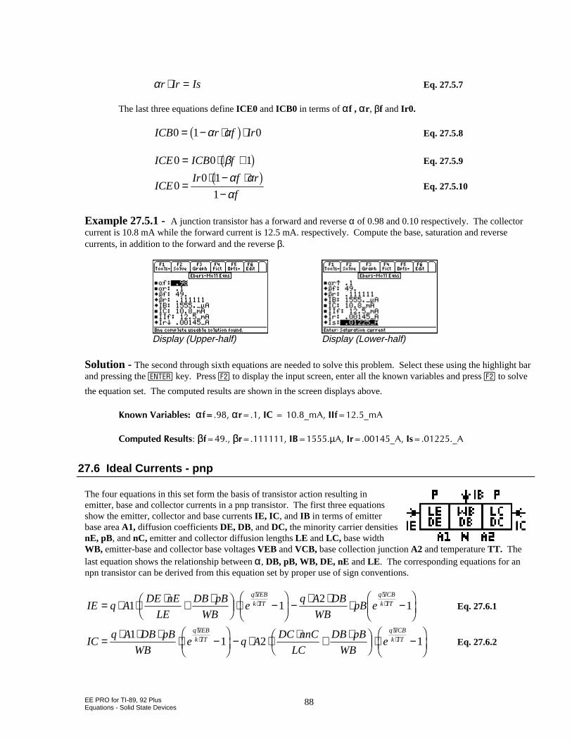
EE PRO for TI-89, 92 PlusEquations - Solid State Devices
88
αr Ir Is⋅ = Eq. 27.5.7
The last three equations define ICE0 and ICB0 in terms of ααf , ααr , βf and Ir0.
ICB r f Ir0 1 0= − ⋅ ⋅α αb g Eq. 27.5.8
ICE ICB f0 0 1= ⋅ +βb g Eq. 27.5.9
ICEIr f r
f0
0 1
1=
⋅ − ⋅−
α αα
b gEq. 27.5.10
Example 27.5.1 - A junction transistor has a forward and reverse α of 0.98 and 0.10 respectively. The collectorcurrent is 10.8 mA while the forward current is 12.5 mA. respectively. Compute the base, saturation and reversecurrents, in addition to the forward and the reverse β.
Display (Upper-half) Display (Lower-half)
Solution - The second through sixth equations are needed to solve this problem. Select these using the highlight barand pressing the key. Press „ to display the input screen, enter all the known variables and press „ to solve
the equation set. The computed results are shown in the screen displays above.
-PQYP8CTKCDNGUααHαT+%AO#++HAO#
%QORWVGF4GUWNVUβHβT+$µ#+TA#+UA#
27.6 Ideal Currents - pnp
The four equations in this set form the basis of transistor action resulting inemitter, base and collector currents in a pnp transistor. The first three equationsshow the emitter, collector and base currents IE, IC , and IB in terms of emitterbase area A1, diffusion coefficients DE, DB, and DC, the minority carrier densitiesnE, pB, and nC, emitter and collector diffusion lengths LE and LC, base widthWB, emitter-base and collector base voltages VEB and VCB, base collection junction A2 and temperature TT. Thelast equation shows the relationship between α, DB, pB, WB, DE, nE and LE. The corresponding equations for annpn transistor can be derived from this equation set by proper use of sign conventions.
IE q ADE nE
LE
DB pB
WBe
q A DB
WBpB e
q VEB
k TT
q VCB
k TT= ⋅ ⋅ ⋅ + ⋅FHG
IKJ ⋅ −FHG
IKJ − ⋅ ⋅ ⋅ −
FHG
IKJ
⋅⋅
⋅⋅1 1
21 Eq. 27.6.1
ICq A DB pB
WBe q A
DC nnC
LC
DB pB
WBe
q VEB
k TT
q VCB
k TT= ⋅ ⋅ ⋅ ⋅ −FHG
IKJ − ⋅ ⋅ ⋅ + ⋅F
HGIKJ ⋅ −FHG
IKJ
⋅⋅
⋅⋅1
1 2 1 Eq. 27.6.2
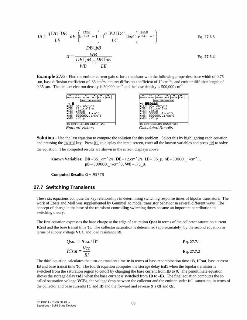
EE PRO for TI-89, 92 PlusEquations - Solid State Devices
89
IBq A DE
LEnE e
q A DC
LCnnC e
q VBE
k TT
q VCB
k TT= ⋅ ⋅ ⋅ ⋅ −FHG
IKJ + ⋅ ⋅ ⋅ −
FHG
IKJ
⋅⋅
⋅⋅1
12
1 Eq. 27.6.3
α =
⋅
⋅ + ⋅
DB pB
WBDB pB
WB
DE nE
LE
Eq. 27.6.4
Example 27.6 - Find the emitter current gain α for a transistor with the following properties: base width of 0.75µm, base diffusion coefficient of 35 cm2/s, emitter diffusion coefficient of 12 cm2/s, and emitter diffusion length of0.35 µm. The emitter electron density is 30,000 cm-3 and the base density is 500,000 cm-3.
Entered Values Calculated Results
Solution - Use the last equation to compute the solution for this problem. Select this by highlighting each equationand pressing the key. Press „ to display the input screen, enter all the known variables and press „ to solve
the equation. The computed results are shown in the screen displays above.
-PQYP8CTKCDNGU&$AEO@U&'EO@U.'AµP'AEO@
R$AEO@9$Aµ
%QORWVGF4GUWNVUαα
27.7 Switching Transients
These six equations compute the key relationships in determining switching response times of bipolar transistors. Thework of Ebers and Moll was supplemented by Gummel to model transistor behavior in several different ways. Theconcept of charge in the base of the transistor controlling switching times became an important contribution toswitching theory.
The first equation expresses the base charge at the edge of saturation Qsat in terms of the collector saturation currentICsat and the base transit time ττt. The collector saturation is determined (approximately) by the second equation interms of supply voltage VCC and load resistance Rl.
Qsat ICsat t= ⋅τ Eq. 27.7.1
ICsatVcc
Rl= Eq. 27.7.2
The third equation calculates the turn-on transient time tr in terms of base recombination time ττB, ICsat, base currentIB and base transit time ττt. The fourth equation computes the storage delay tsd1 when the bipolar transistor isswitched from the saturation region to cutoff by changing the base current from IB to 0. The penultimate equationshows the storage delay tsd2 when the base current is switched from IB to -IB . The final equation computes the socalled saturation voltage VCEs, the voltage drop between the collector and the emitter under full saturation, in terms ofthe collector and base currents IC and IB and the forward and reverse α’s ααf and ααr .
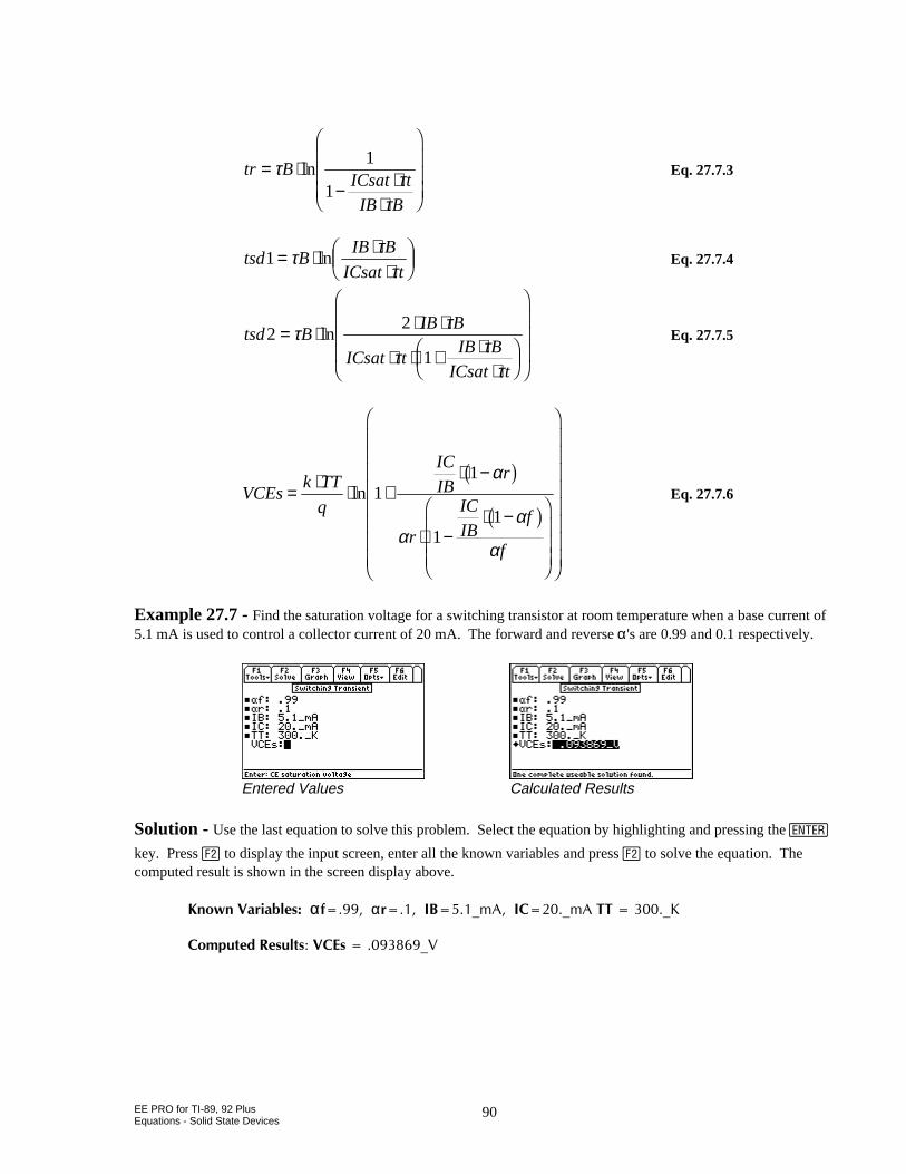
EE PRO for TI-89, 92 PlusEquations - Solid State Devices
90
tr BICsat t
IB B
= ⋅− ⋅
⋅
F
H
GGG
I
K
JJJ
τ ττ
ln1
1Eq. 27.7.3
tsd BIB B
ICsat t1= ⋅ ⋅
⋅FHG
IKJτ τ
τln Eq. 27.7.4
tsd BIB B
ICsat tIB B
ICsat t
22
1= ⋅ ⋅ ⋅
⋅ ⋅ + ⋅⋅
FHG
IKJ
F
H
GGG
I
K
JJJ
τ τ
τ ττ
ln Eq. 27.7.5
VCEsk TT
q
IC
IBr
r
IC
IBf
f
= ⋅ ⋅ +⋅ −
⋅ −⋅ −F
HGGG
I
KJJJ
F
H
GGGGGGGG
I
K
JJJJJJJJ
ln 11
11
α
αα
α
b g
b gEq. 27.7.6
Example 27.7 - Find the saturation voltage for a switching transistor at room temperature when a base current of5.1 mA is used to control a collector current of 20 mA. The forward and reverse α's are 0.99 and 0.1 respectively.
Entered Values Calculated Results
Solution - Use the last equation to solve this problem. Select the equation by highlighting and pressing the ¸
key. Press „ to display the input screen, enter all the known variables and press „ to solve the equation. Thecomputed result is shown in the screen display above.
-PQYP8CTKCDNGUααHαT+$AO#+%AO#66A-
%QORWVGF4GUWNVU8%'UA8
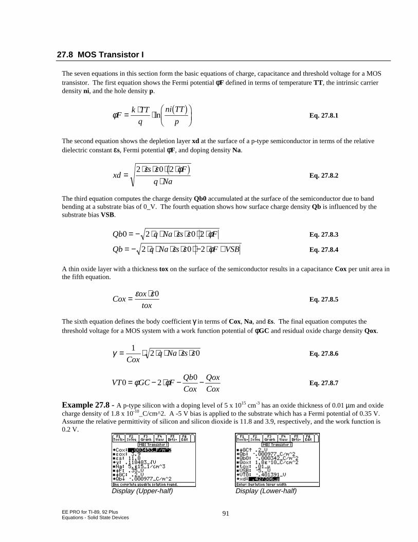
EE PRO for TI-89, 92 PlusEquations - Solid State Devices
91
27.8 MOS Transistor I
The seven equations in this section form the basic equations of charge, capacitance and threshold voltage for a MOStransistor. The first equation shows the Fermi potential φF defined in terms of temperature TT , the intrinsic carrierdensity ni, and the hole density p.
φFk TT
q
ni TT
p= ⋅ ⋅
FHG
IKJln
b gEq. 27.8.1
The second equation shows the depletion layer xd at the surface of a p-type semiconductor in terms of the relativedielectric constant εs, Fermi potential φF, and doping density Na.
xds F
q Na=
⋅ ⋅ ⋅ ⋅⋅
2 0 2ε ε φb gEq. 27.8.2
The third equation computes the charge density Qb0 accumulated at the surface of the semiconductor due to bandbending at a substrate bias of 0_V. The fourth equation shows how surface charge density Qb is influenced by thesubstrate bias VSB.
Qb q Na s F0 2 0 2= − ⋅ ⋅ ⋅ ⋅ ⋅ ⋅ε ε φ Eq. 27.8.3
Qb q Na s F VSB= − ⋅ ⋅ ⋅ ⋅ ⋅ − ⋅ +2 0 2ε ε φ Eq. 27.8.4
A thin oxide layer with a thickness tox on the surface of the semiconductor results in a capacitance Cox per unit area inthe fifth equation.
Coxox
tox= ⋅ε ε0
Eq. 27.8.5
The sixth equation defines the body coefficient γ in terms of Cox, Na, and εs. The final equation computes thethreshold voltage for a MOS system with a work function potential of φGC and residual oxide charge density Qox.
γ ε ε= ⋅ ⋅ ⋅ ⋅ ⋅12 0
Coxq Na s Eq. 27.8.6
VT GC FQb
Cox
Qox
Cox0 2
0= − ⋅ − −φ φ Eq. 27.8.7
Example 27.8 - A p-type silicon with a doping level of 5 x 1015 cm-3 has an oxide thickness of 0.01 µm and oxidecharge density of 1.8 x 10⁻¹⁰_C/cm^2. A -5 V bias is applied to the substrate which has a Fermi potential of 0.35 V.Assume the relative permittivity of silicon and silicon dioxide is 11.8 and 3.9, respectively, and the work function is0.2 V.
Display (Upper-half) Display (Lower-half)
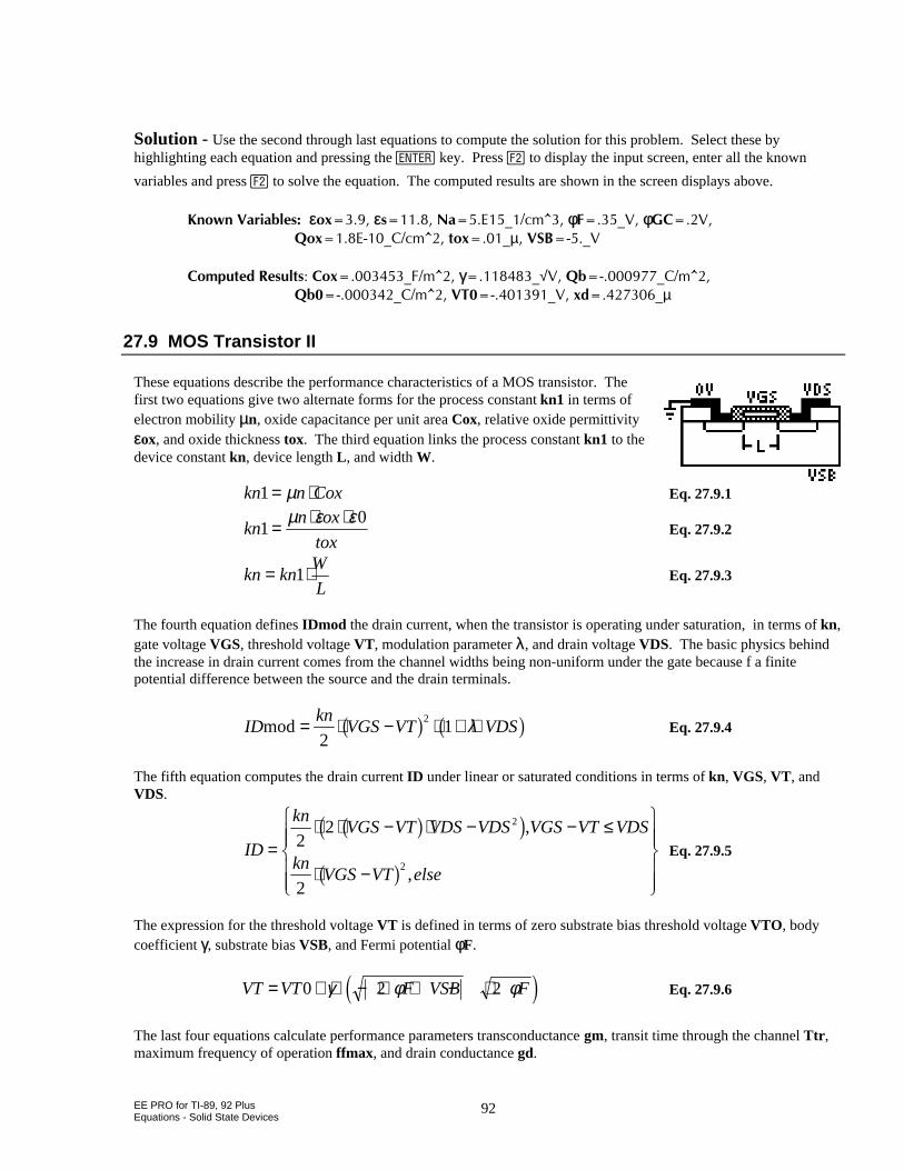
EE PRO for TI-89, 92 PlusEquations - Solid State Devices
92
Solution - Use the second through last equations to compute the solution for this problem. Select these byhighlighting each equation and pressing the key. Press „ to display the input screen, enter all the known
variables and press „ to solve the equation. The computed results are shown in the screen displays above.
-PQYP8CTKCDNGUεQZεU0C'AEO@φ(A8φ)%8
3QZ'A%EO@VQZAµ85$A8
%QORWVGF4GUWNVU%QZA(O@γA√83DA%O@
3DA%O@86A8ZFAµ
27.9 MOS Transistor II
These equations describe the performance characteristics of a MOS transistor. Thefirst two equations give two alternate forms for the process constant kn1 in terms ofelectron mobility µn, oxide capacitance per unit area Cox, relative oxide permittivityεox, and oxide thickness tox. The third equation links the process constant kn1 to thedevice constant kn, device length L , and width W.
kn n Cox1= ⋅µ Eq. 27.9.1
knn ox
tox1
0= ⋅ ⋅µ ε εEq. 27.9.2
kn knW
L= ⋅1 Eq. 27.9.3
The fourth equation defines IDmod the drain current, when the transistor is operating under saturation, in terms of kn,gate voltage VGS, threshold voltage VT , modulation parameter λ, and drain voltage VDS. The basic physics behindthe increase in drain current comes from the channel widths being non-uniform under the gate because f a finitepotential difference between the source and the drain terminals.
IDkn
VGS VT VDSmod= ⋅ − ⋅ + ⋅2
12b g b gλ Eq. 27.9.4
The fifth equation computes the drain current ID under linear or saturated conditions in terms of kn, VGS, VT , andVDS.
ID
knVGS VT VDS VDS VGS VT VDS
knVGS VT else
=⋅ ⋅ − ⋅ − − ≤
⋅ −
RS||
T||
UV||
W||
22
2
2
2
b gc h
b g
,
,Eq. 27.9.5
The expression for the threshold voltage VT is defined in terms of zero substrate bias threshold voltage VTO , bodycoefficient γγ, substrate bias VSB, and Fermi potential φφF.
VT VT F VSB F= + ⋅ − ⋅ + − ⋅0 2 2γ φ φe j Eq. 27.9.6
The last four equations calculate performance parameters transconductance gm, transit time through the channel Ttr ,maximum frequency of operation ffmax, and drain conductance gd.
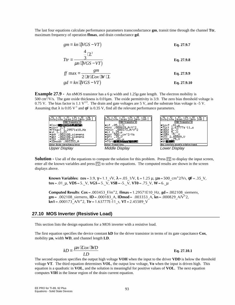
EE PRO for TI-89, 92 PlusEquations - Solid State Devices
93
The last four equations calculate performance parameters transconductance gm, transit time through the channel Ttr ,maximum frequency of operation ffmax, and drain conductance gd.
gm kn VGS VT= ⋅ −b g Eq. 27.9.7
TtrL
n VGS VT=
⋅
⋅ −
43
2
µ b g Eq. 27.9.8
ffgm
Cox W Lmax=
⋅ ⋅ ⋅ ⋅2 πEq. 27.9.9
gd kn VGS VT= ⋅ −b g Eq. 27.9.10
Example 27.9 - An nMOS transistor has a 6 µ width and 1.25µ gate length. The electron mobility is500 cm2/V/s. The gate oxide thickness is 0.01µm. The oxide permittivity is 3.9. The zero bias threshold voltage is0.75 V. The bias factor is 1.1 V1/2. The drain and gate voltages are 5 V, and the substrate bias voltage is -5 V.Assuming that λ is 0.05 V-1 and φF is 0.35 V, find all the relevant performance parameters.
Upper Display Middle Display Lower Display
Solution - Use all of the equations to compute the solution for this problem. Press „ to display the input screen,enter all the known variables and press „ to solve the equations. The computed results are shown in the screendisplays above.
-PQYP8CTKCDNGUεQZγγA√8λλA8.µµµPAEO@8Uφφ(A8
VQZAµ8&5A88)5A885$A886A89Aµ
%QORWVGF4GUWNVU%QZA(O@HHOCZ'A*\IFAUKGOGPUIOAUKGOGPU+&A#+&OQFA#MPA#8@MPA#8@6VT'AU86A8
27.10 MOS Inverter (Resistive Load)
This section lists the design equations for a MOS inverter with a resistive load.
The first equation specifies the device constant kD for the driver transistor in terms of its gate capacitance Cox,mobility µn, width WD, and channel length LD .
kDn Cox WD
LD= ⋅ ⋅µ
Eq. 27.10.1
The second equation specifies the output high voltage VOH when the input to the driver VDD is below the thresholdvoltage VT . The third equation determines VOL , the output low voltage, Vo when the input is driven high. Thisequation is a quadratic in VOL , and the solution is meaningful for positive values of VOL . The next equationcomputes VIH in the linear region of the drain current equation.
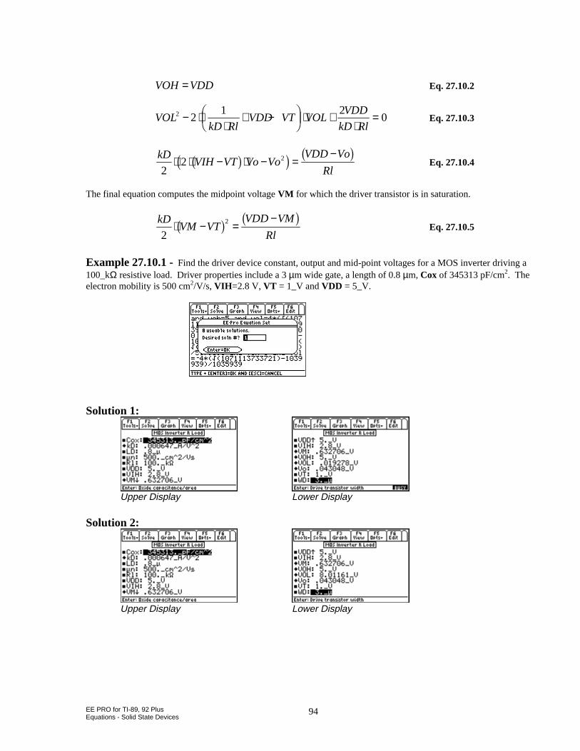
EE PRO for TI-89, 92 PlusEquations - Solid State Devices
94
VOH VDD= Eq. 27.10.2
VOLkD Rl
VDD VT VOLVDD
kD Rl2 2
1 20− ⋅
⋅+ −F
HGIKJ ⋅ +
⋅= Eq. 27.10.3
kDVIH VT Vo Vo
VDD Vo
Rl22 2⋅ ⋅ − ⋅ − =
−b gc h b gEq. 27.10.4
The final equation computes the midpoint voltage VM for which the driver transistor is in saturation.
kDVM VT
VDD VM
Rl22⋅ − =
−b g b gEq. 27.10.5
Example 27.10.1 - Find the driver device constant, output and mid-point voltages for a MOS inverter driving a100_kΩ resistive load. Driver properties include a 3 µm wide gate, a length of 0.8 µm, Cox of 345313 pF/cm2. Theelectron mobility is 500 cm2/V/s, VIH =2.8 V, VT = 1_V and VDD = 5_V.
Solution 1:
Upper Display Lower Display
Solution 2:
Upper Display Lower Display
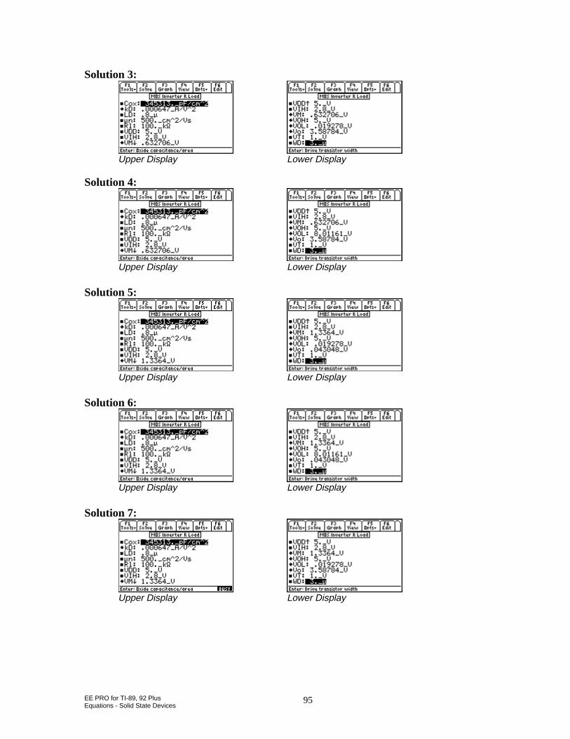
EE PRO for TI-89, 92 PlusEquations - Solid State Devices
95
Solution 3:
Upper Display Lower Display
Solution 4:
Upper Display Lower Display
Solution 5:
Upper Display Lower Display
Solution 6:
Upper Display Lower Display
Solution 7:
Upper Display Lower Display
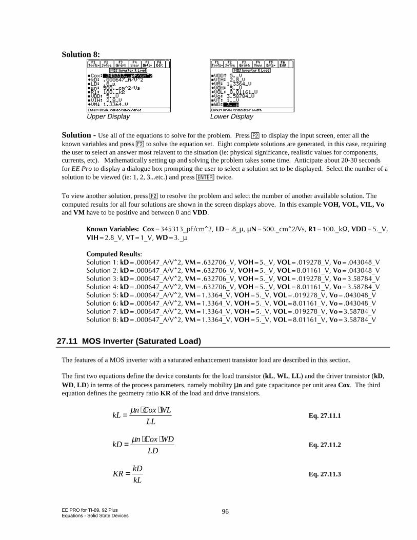
EE PRO for TI-89, 92 PlusEquations - Solid State Devices
96
Solution 8:
Upper Display Lower Display
Solution - Use all of the equations to solve for the problem. Press „ to display the input screen, enter all theknown variables and press „ to solve the equation set. Eight complete solutions are generated, in this case, requiringthe user to select an answer most relavent to the situation (ie: physical significance, realistic values for components,currents, etc). Mathematically setting up and solving the problem takes some time. Anticipate about 20-30 secondsfor EE¹Pro to display a dialogue box prompting the user to select a solution set to be displayed. Select the number of asolution to be viewed (ie: 1, 2, 3...etc.) and press twice.
To view another solution, press „ to resolve the problem and select the number of another available solution. Thecomputed results for all four solutions are shown in the screen displays above. In this example VOH, VOL, VIL, Voand VM have to be positive and between 0 and VDD.
-PQYP8CTKCDNGU%QZAR(EO@.&Aµµ0AEO@8U4AMΩ8&&A8
8+*A886A89&Aµ
%QORWVGF4GUWNVU5QNWVKQPM&A#8@8/A881*A881.A88QA85QNWVKQPM&A#8@8/A881*A881.A88QA85QNWVKQPM&A#8@8/A881*A881.A88QA85QNWVKQPM&A#8@8/A881*A881.A88QA85QNWVKQPM&A#8@8/A881*A881.A88QA85QNWVKQPM&A#8@8/A881*A881.A88QA85QNWVKQPM&A#8@8/A881*A881.A88QA85QNWVKQPM&A#8@8/A881*A881.A88QA8
27.11 MOS Inverter (Saturated Load)
The features of a MOS inverter with a saturated enhancement transistor load are described in this section.
The first two equations define the device constants for the load transistor (kL , WL , LL ) and the driver transistor (kD,WD, LD ) in terms of the process parameters, namely mobility µn and gate capacitance per unit area Cox. The thirdequation defines the geometry ratio KR of the load and drive transistors.
kLn Cox WL
LL= ⋅ ⋅µ
Eq. 27.11.1
kDn Cox WD
LD= ⋅ ⋅µ
Eq. 27.11.2
KRkD
kL= Eq. 27.11.3
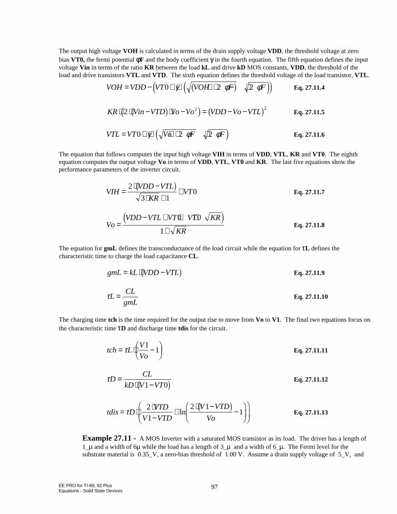
EE PRO for TI-89, 92 PlusEquations - Solid State Devices
97
The output high voltage VOH is calculated in terms of the drain supply voltage VDD, the threshold voltage at zerobias VT0, the fermi potential φF and the body coefficient γ in the fourth equation. The fifth equation defines the inputvoltage Vin in terms of the ratio KR between the load kL and drive kD MOS constants, VDD, the threshold of theload and drive transistors VTL and VTD . The sixth equation defines the threshold voltage of the load transistor, VTL .
VOH VDD VT VOH F F= − + ⋅ + ⋅ − ⋅0 2 2γ φ φb ge je j Eq. 27.11.4
KR Vin VTD Vo Vo VDD Vo VTL⋅ ⋅ − ⋅ − = − −2 2 2b gc h b g Eq. 27.11.5
VTL VT Vo F F= + ⋅ + ⋅ − ⋅0 2 2γ φ φd i Eq. 27.11.6
The equation that follows computes the input high voltage VIH in terms of VDD, VTL , KR and VT0. The eighthequation computes the output voltage Vo in terms of VDD, VTL , VT0 and KR . The last five equations show theperformance parameters of the inverter circuit.
VIHVDD VTL
KRVT=
⋅ −⋅ +
+2
3 10
b gEq. 27.11.7
VoVDD VTL VT VT KR
KR=
− + + ⋅
+
0 0
1
d iEq. 27.11.8
The equation for gmL defines the transconductance of the load circuit while the equation for τL defines thecharacteristic time to charge the load capacitance CL .
gmL kL VDD VTL= ⋅ −b g Eq. 27.11.9
τLCL
gmL= Eq. 27.11.10
The charging time tch is the time required for the output rise to move from Vo to V1. The final two equations focus onthe characteristic time τD and discharge time tdis for the circuit.
tch LV
Vo= ⋅ −F
HGIKJτ 1
1 Eq. 27.11.11
τDCL
kD V VT=
⋅ −1 0b g Eq. 27.11.12
tdis DVTD
V VTD
V VTD
Vo= ⋅ ⋅
−+
⋅ −−
FHG
IKJ
FHG
IKJτ 2
1
2 11ln
b gEq. 27.11.13
Example 27.11 - A MOS Inverter with a saturated MOS transistor as its load. The driver has a length of1_µ and a width of 6µ while the load has a length of 3_µ and a width of 6_µ. The Fermi level for thesubstrate material is 0.35_V, a zero-bias threshold of 1.00 V. Assume a drain supply voltage of 5_V, and
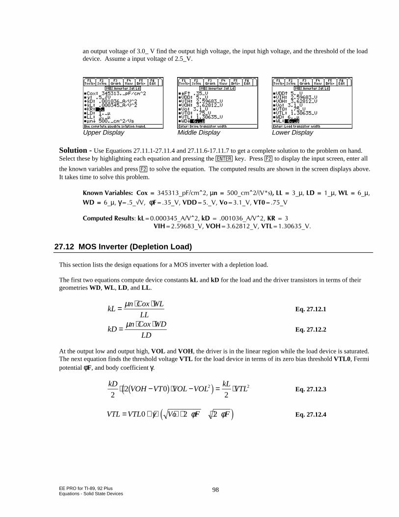
EE PRO for TI-89, 92 PlusEquations - Solid State Devices
98
an output voltage of 3.0_ V find the output high voltage, the input high voltage, and the threshold of the loaddevice. Assume a input voltage of 2.5_V.
Upper Display Middle Display Lower Display
Solution - Use Equations 27.11.1-27.11.4 and 27.11.6-17.11.7 to get a complete solution to the problem on hand.Select these by highlighting each equation and pressing the key. Press „ to display the input screen, enter all
the known variables and press „ to solve the equation. The computed results are shown in the screen displays above.It takes time to solve this problem.
-PQYP8CTKCDNGU%QZAR(EO@µ[email protected]µ.&Aµ9.Aµ9&AµγA√8φφ(A88&&A88QA886A8
%QORWVGF4GUWNVUM.A#8@M&A#8@-48+*A881*A886.A8
27.12 MOS Inverter (Depletion Load)
This section lists the design equations for a MOS inverter with a depletion load.
The first two equations compute device constants kL and kD for the load and the driver transistors in terms of theirgeometries WD, WL , LD , and LL .
kLn Cox WL
LL= ⋅ ⋅µ
Eq. 27.12.1
kDn Cox WD
LD= ⋅ ⋅µ
Eq. 27.12.2
At the output low and output high, VOL and VOH , the driver is in the linear region while the load device is saturated.The next equation finds the threshold voltage VTL for the load device in terms of its zero bias threshold VTL0 , Fermipotential φφF, and body coefficient γγ.
kDVOH VT VOL VOL
kLVTL
22 0
22 2⋅ − ⋅ − = ⋅b gc h Eq. 27.12.3
VTL VTL Vo F F= + ⋅ + ⋅ − ⋅0 2 2γ φ φd i Eq. 27.12.4
EE PRO for TI-89, 92 PlusEquations - Solid State Devices
99
The charging time tch for the CL is defined next. The current in the depletion load I0 is given by the last equation.
tchCL VL
I= ⋅
0Eq. 27.12.5
I kL VTL0 2= ⋅ Eq. 27.12.6
Example 27.12 - A MOS inverter with a depletion mode transistor as the load has a driver transistor 5_µ wide and1_µ long while the load is a depletion mode device with a 0 bias threshold of -4_V, 3_µ long and 3_µ wide. Given anelectron mobility of 500_cm^2/(V*s) and a depletion threshold of -4_V; for the load device, compute VOH and VTLwhen the output voltage is 2.5_V. Assume VOL to be .4_V and .5 for γ.
Solution 1: Upper Display Solution 1: Lower Display
Solution 2: Upper Display Solution 2: Lower Display
Solution - The problem can be solved when equations 27.12.1 - 27.12.4 are selected. Highlight each of these andpress . Press „ to display the input screen, enter all the known variables and press „ to solve the equations.
Two complete solutions are computed for this case and are shown in the screen displays above.
-PQYP8CTKCDNGU%QZAR(EO@γA8@.&Aµ..AµµPAEO@8Uφ(A881*A88QA886A8
86.A89&Aµ9.Aµ
%QORWVGF4GUWNVU5QNWVKQPM&A#[email protected]#[email protected]&A#[email protected]#[email protected]
27.13 CMOS Transistor Pair
These five equations describe the properties of a CMOS inverter. The first twoequations compute device parameters for n and p channel devices. The second pairof equations compute input voltages VIH and VIL . The last equation computes Vinwhen the n-channel driver is in saturation and the p-channel device is in the linearregion.
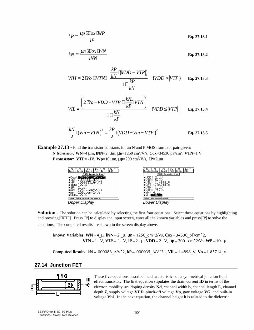
EE PRO for TI-89, 92 PlusEquations - Solid State Devices
100
kPp Cox WP
lP= ⋅ ⋅µ
Eq. 27.13.1
kNn Cox WN
lNN= ⋅ ⋅µ
Eq. 27.13.2
VIH Vo VTN
kP
kNVDD VTP
kP
kN
= ⋅ + +⋅ −
+2
1
c h VDD VTP> Eq. 27.13.3
VILVo VDD VTP
kN
kPVTN
kN
kP
=⋅ − − + ⋅F
HGIKJ
+
2
1 VDD VTP≤ Eq. 27.13.4
kNVin VTN
kPVDD Vin VTP
2 22 2
⋅ − = ⋅ − −b g c h Eq. 27.13.5
Example 27.13 - Find the transistor constants for an N and P MOS transistor pair given:N transistor: WN=4 µm, lNN=2. µm, µµn=1250 cm2/V/s, Cox=34530 pF/cm2, VTN=1 VP transistor: VTP= -1V, Wp=10 µm, µµp=200 cm2/V/s, lP=2µm
Upper Display Lower Display
Solution - The solution can be calculated by selecting the first four equations. Select these equations by highlightingand pressing . Press „ to display the input screen, enter all the known variables and press „ to solve the
equations. The computed results are shown in the screen display above.
-PQYP8CTKCDNGU90AµN00AµµµPAEO@8U%QZAR(EO@
860A8862A8N2Aµ8&&A8µµRAEO@8U92Aµ
%QORWVGF4GUWNVUM0A#8@M2A#8@8+.A88QA8
27.14 Junction FET
These five equations describe the characteristics of a symmetrical junction fieldeffect transistor. The first equation stipulates the drain current ID in terms of theelectron mobility µµn, doping density Nd, channel width b, channel length L , channeldepth Z, supply voltage VDD, pinch-off voltage Vp, gate voltage VG, and built-involtage Vbi . In the next equation, the channel height b is related to the dielectric
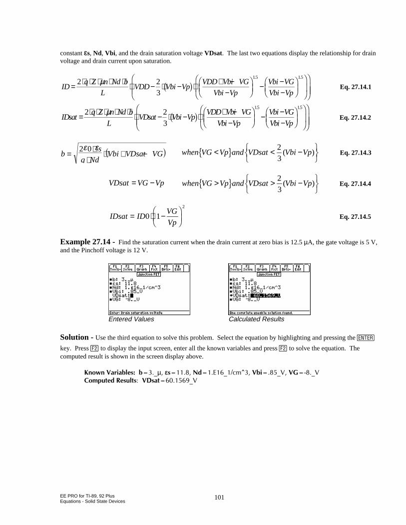
EE PRO for TI-89, 92 PlusEquations - Solid State Devices
101
constant εs, Nd, Vbi , and the drain saturation voltage VDsat. The last two equations display the relationship for drainvoltage and drain current upon saturation.
IDq Z n Nd b
LVDD Vbi Vp
VDD Vbi VG
Vbi Vp
Vbi VG
Vbi Vp= ⋅ ⋅ ⋅ ⋅ ⋅ ⋅ − ⋅ − ⋅ + −
−FHG
IKJ − −
−FHG
IKJ
FHG
IKJ
FHGG
IKJJ
2 2
3
15 15µ b g
. .
Eq. 27.14.1
IDsatq Z n Nd b
LVDsat Vbi Vp
VDD Vbi VG
Vbi Vp
Vbi VG
Vbi Vp= ⋅ ⋅ ⋅ ⋅ ⋅ ⋅ − ⋅ − ⋅ + −
−FHG
IKJ − −
−FHG
IKJ
FHG
IKJ
FHGG
IKJJ
2 2
3
15 15µ b g
. .
Eq. 27.14.2
bs
q NdVbi VDsat VG= ⋅
⋅⋅ + −
2 0ε ε1 6 when VG Vp and VDsat Vbi Vp< < −RST
UVWl q 2
3( ) Eq. 27.14.3
VDsat VG Vp= − when VG Vp and VDsat Vbi Vp> > −RSTUVWl q 2
3( ) Eq. 27.14.4
IDsat IDVG
Vp= ⋅ −
FHG
IKJ0 1
2
Eq. 27.14.5
Example 27.14 - Find the saturation current when the drain current at zero bias is 12.5 µA, the gate voltage is 5 V,and the Pinchoff voltage is 12 V.
Entered Values Calculated Results
Solution - Use the third equation to solve this problem. Select the equation by highlighting and pressing the ¸
key. Press „ to display the input screen, enter all the known variables and press „ to solve the equation. Thecomputed result is shown in the screen display above.
-PQYP8CTKCDNGUDAµεU0F'AEO@8DKA88)A8%QORWVGF4GUWNVU8&UCVA8
EE PRO for TI - 89, 92 PlusEquations - Linear Amplifiers
102
Chapter 28 Linear AmplifiersThis section covers linear circuit models (i.e., small signal models) used in making first order calculations usingbipolar or junction transistors in amplifier circuits. These circuit models are referred to by many different namessuch as small signal circuit model, AC circuit model, linear circuit model. In addition, popular deviceconfigurations such as the Darlington pair, emitter-coupled pair, differential amplifier, and a source-coupled pairtopics have been included.
BJT (Common Base)BJT (Common Emitter)BJT (Common Collector)FET (Common Gate)FET (Common Source)FET (Common Drain)
Darlington (CC-CC)Darlington (CC-CE)Emitter-Coupled AmplifierDifferential AmplifierSource-Coupled JFET Pair
Variables
The table lists all variables used in this section along with a description and appropriate units.
Variable Description Unitα0 Current gain, CE unitlessAc Common mode gain unitlessAd Differential mode gain unitlessAi Current gain, CB unitlessAov Overall voltage gain unitlessAv Voltage gain, CC/CD unitlessβ0 Current gain, CB unitlessCMRR Common mode reject ratio unitlessgm Transconductance Sµ Amplification factor unitlessrb Base resistance Ωrrc Collector resistance Ωrd Drain resistance Ωre Emitter resistance ΩRBA External base resistance ΩRCA External collector resistance ΩRDA External drain resistance ΩREA External emitter resistance ΩRG External gate resistance ΩRic Common mode input resistance ΩRid Differential input resistance Ω
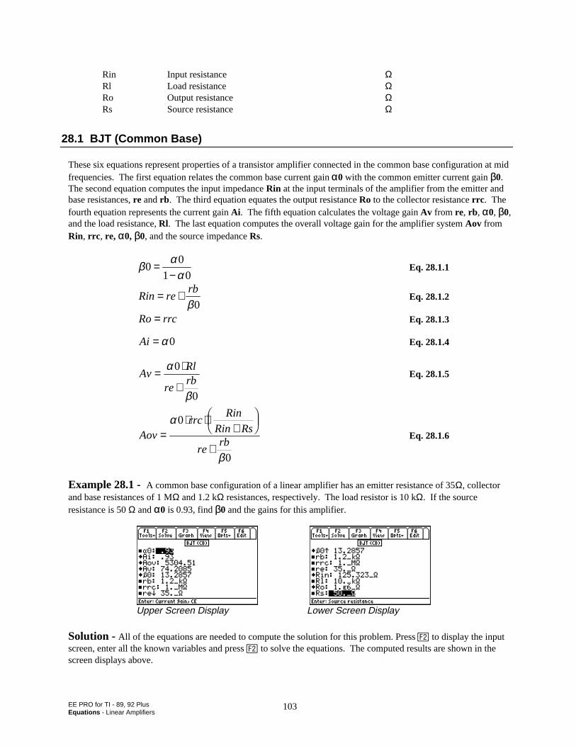
EE PRO for TI - 89, 92 PlusEquations - Linear Amplifiers
103
Rin Input resistance ΩRl Load resistance ΩRo Output resistance ΩRs Source resistance Ω
28.1 BJT (Common Base)
These six equations represent properties of a transistor amplifier connected in the common base configuration at midfrequencies. The first equation relates the common base current gain α0 with the common emitter current gain β0.The second equation computes the input impedance Rin at the input terminals of the amplifier from the emitter andbase resistances, re and rb . The third equation equates the output resistance Ro to the collector resistance rrc . Thefourth equation represents the current gain Ai . The fifth equation calculates the voltage gain Av from re, rb , α0, β0,and the load resistance, Rl. The last equation computes the overall voltage gain for the amplifier system Aov fromRin, rrc , re, α0, β0, and the source impedance Rs.
β αα
00
1 0=
−Eq. 28.1.1
Rin rerb= +β0
Eq. 28.1.2
Ro rrc= Eq. 28.1.3
Ai = α0 Eq. 28.1.4
AvRl
rerb
= ⋅
+
α
β
0
0
Eq. 28.1.5
Aovrrc
Rin
Rin Rs
rerb
=⋅ ⋅
+FHG
IKJ
+
α
β
0
0
Eq. 28.1.6
Example 28.1 - A common base configuration of a linear amplifier has an emitter resistance of 35Ω, collectorand base resistances of 1 MΩ and 1.2 kΩ resistances, respectively. The load resistor is 10 kΩ. If the sourceresistance is 50 Ω and αα0 is 0.93, find ββ0 and the gains for this amplifier.
Upper Screen Display Lower Screen Display
Solution - All of the equations are needed to compute the solution for this problem. Press „ to display the inputscreen, enter all the known variables and press „ to solve the equations. The computed results are shown in thescreen displays above.
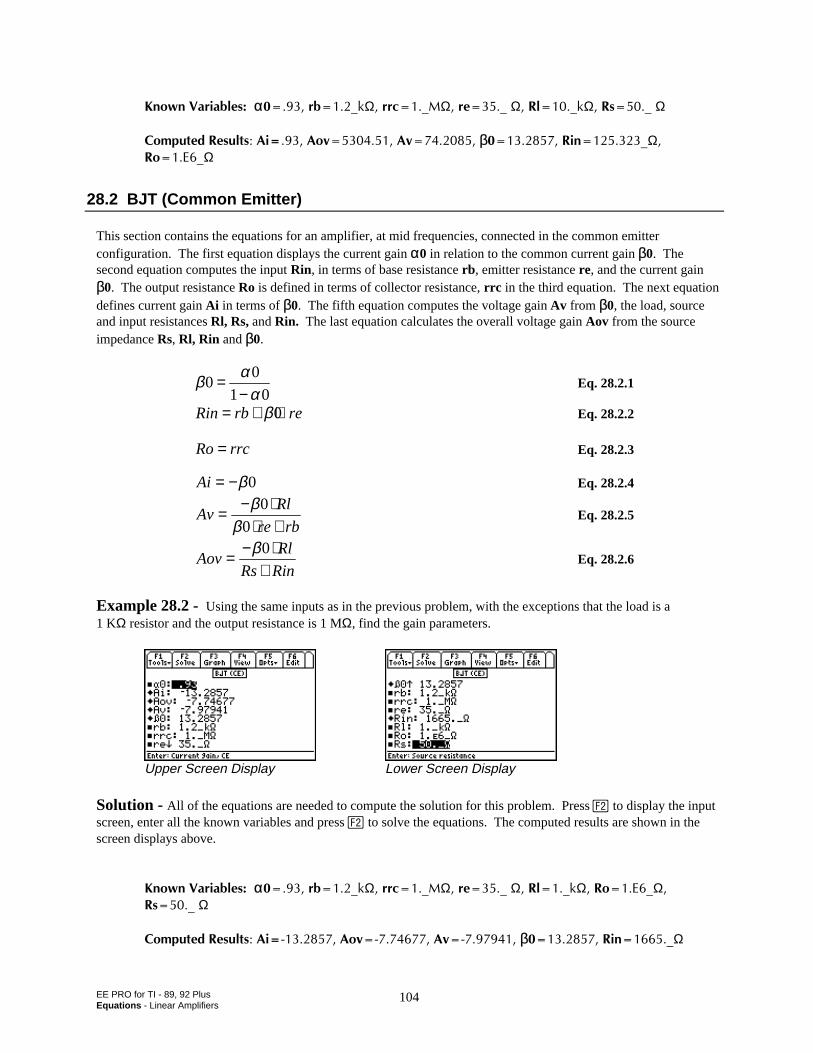
EE PRO for TI - 89, 92 PlusEquations - Linear Amplifiers
104
-PQYP8CTKCDNGUαTDAMΩTTEA/ΩTGAΩ4NAMΩ4UAΩ
%QORWVGF4GUWNVU#K#QX#Xβ4KPAΩ
4Q'AΩ
28.2 BJT (Common Emitter)
This section contains the equations for an amplifier, at mid frequencies, connected in the common emitterconfiguration. The first equation displays the current gain αα0 in relation to the common current gain ββ0. Thesecond equation computes the input Rin, in terms of base resistance rb , emitter resistance re, and the current gainββ0. The output resistance Ro is defined in terms of collector resistance, rrc in the third equation. The next equationdefines current gain Ai in terms of ββ0. The fifth equation computes the voltage gain Av from ββ0, the load, sourceand input resistances Rl, Rs, and Rin. The last equation calculates the overall voltage gain Aov from the sourceimpedance Rs, Rl, Rin and ββ0.
β αα
00
1 0=
−Eq. 28.2.1
Rin rb re= + ⋅β0 Eq. 28.2.2
Ro rrc= Eq. 28.2.3
Ai = −β0 Eq. 28.2.4
AvRl
re rb= − ⋅
⋅ +β
β0
0Eq. 28.2.5
AovRl
Rs Rin= − ⋅
+β0
Eq. 28.2.6
Example 28.2 - Using the same inputs as in the previous problem, with the exceptions that the load is a1 KΩ resistor and the output resistance is 1 MΩ, find the gain parameters.
Upper Screen Display Lower Screen Display
Solution - All of the equations are needed to compute the solution for this problem. Press „ to display the inputscreen, enter all the known variables and press „ to solve the equations. The computed results are shown in thescreen displays above.
-PQYP8CTKCDNGUααTDAMΩTTEA/ΩTGAΩ4NAMΩ4Q'AΩ
4UAΩ
%QORWVGF4GUWNVU#K#QX#Xβ4KPAΩ
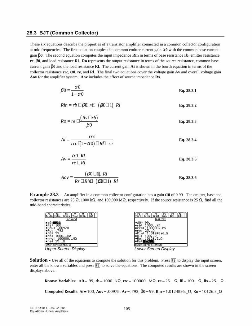
EE PRO for TI - 89, 92 PlusEquations - Linear Amplifiers
105
28.3 BJT (Common Collector)
These six equations describe the properties of a transistor amplifier connected in a common collector configurationat mid frequencies. The first equation couples the common emitter current gain α0 with the common base currentgain β0. The second equation computes the input impedance Rin in terms of base resistance rb , emitter resistancere, β0, and load resistance Rl. Ro represents the output resistance in terms of the source resistance, common basecurrent gain β0 and the load resistance Rl. The current gain Ai is shown in the fourth equation in terms of thecollector resistance rrc , α0, re, and Rl. The final two equations cover the voltage gain Av and overall voltage gainAov for the amplifier system. Aov includes the effect of source impedance Rs.
β αα
00
1 0=
−Eq. 28.3.1
Rin rb re Rl= + ⋅ + + ⋅β β0 0 1b g Eq. 28.3.2
Ro reRs rb
= ++b g
β0Eq. 28.3.3
Airrc
rrc Rl re=
⋅ − + +1 0αb g Eq. 28.3.4
AvRl
re Rl= ⋅
+α0
Eq. 28.3.5
AovRl
Rs Rin Rl=
+ ⋅+ + + ⋅
ββ
0 1
0 1
b gb g Eq. 28.3.6
Example 28.3 - An amplifier in a common collector configuration has a gain α0 of 0.99. The emitter, base andcollector resistances are 25 Ω, 1000 kΩ, and 100,000 MΩrespectively. If the source resistance is 25 Ωfind all themid-band characteristics.
Upper Screen Display Lower Screen Display
Solution - Use all of the equations to compute the solution for this problem. Press „ to display the input screen,enter all the known variables and press „ to solve the equations. The computed results are shown in the screendisplays above.
-PQYP8CTKCDNGUαTDAMΩTTEA/ΩTGAΩ4NAΩ4UAΩ
%QORWVGF4GUWNVU#K#QX#Xβ4KP'AΩ4QAΩ
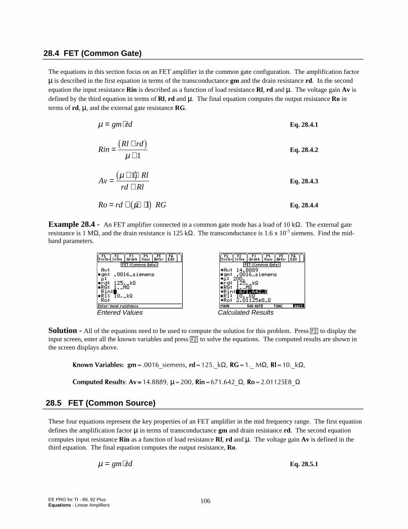
EE PRO for TI - 89, 92 PlusEquations - Linear Amplifiers
106
28.4 FET (Common Gate)
The equations in this section focus on an FET amplifier in the common gate configuration. The amplification factorµ is described in the first equation in terms of the transconductance gm and the drain resistance rd . In the secondequation the input resistance Rin is described as a function of load resistance Rl, rd and µ. The voltage gain Av isdefined by the third equation in terms of Rl, rd and µ. The final equation computes the output resistance Ro interms of rd , µ, and the external gate resistance RG.
µ = ⋅gm rd Eq. 28.4.1
RinRl rd
=++
b gµ 1
Eq. 28.4.2
AvRl
rd Rl=
+ ⋅+
µ 1b gEq. 28.4.3
Ro rd RG= + + ⋅µ 1b g Eq. 28.4.4
Example 28.4 - An FET amplifier connected in a common gate mode has a load of 10 kΩ. The external gateresistance is 1 MΩ, and the drain resistance is 125 kΩ. The transconductance is 1.6 x 10⁻³ siemens. Find the mid-band parameters.
Entered Values Calculated Results
Solution - All of the equations need to be used to compute the solution for this problem. Press „ to display theinput screen, enter all the known variables and press „ to solve the equations. The computed results are shown inthe screen displays above.
-PQYP8CTKCDNGUIOAUKGOGPUTFAMΩ4)A/Ω4NAMΩ
%QORWVGF4GUWNVU#Xµµ4KPAΩ4Q'AΩ
28.5 FET (Common Source)
These four equations represent the key properties of an FET amplifier in the mid frequency range. The first equationdefines the amplification factor µµ in terms of transconductance gm and drain resistance rd . The second equationcomputes input resistance Rin as a function of load resistance Rl, rd and µµ. The voltage gain Av is defined in thethird equation. The final equation computes the output resistance, Ro.
µ = ⋅gm rd Eq. 28.5.1
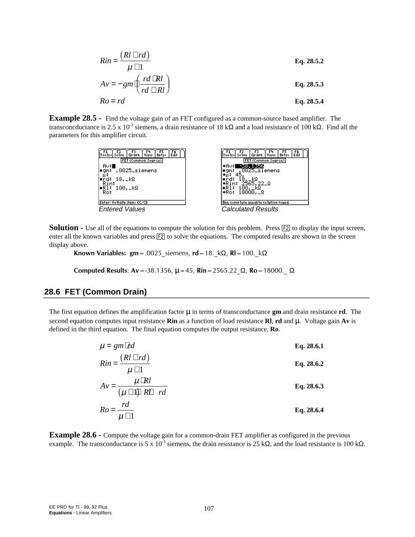
EE PRO for TI - 89, 92 PlusEquations - Linear Amplifiers
107
RinRl rd
=++
b gµ 1
Eq. 28.5.2
Av gmrd Rl
rd Rl= − ⋅ ⋅
+FHG
IKJ Eq. 28.5.3
Ro rd= Eq. 28.5.4
Example 28.5 - Find the voltage gain of an FET configured as a common-source based amplifier. Thetransconcductance is 2.5 x 10⁻³ siemens, a drain resistance of 18 kΩ and a load resistance of 100 kΩ. Find all theparameters for this amplifier circuit.
Entered Values Calculated Results
Solution - Use all of the equations to compute the solution for this problem. Press „ to display the input screen,enter all the known variables and press „ to solve the equations. The computed results are shown in the screendisplay above.
-PQYP8CTKCDNGUIOAUKGOGPUTFAMΩ4NAMΩ
%QORWVGF4GUWNVU#Xµµ4KPAΩ4QAΩ
28.6 FET (Common Drain)
The first equation defines the amplification factor µµ in terms of transconductance gm and drain resistance rd . Thesecond equation computes input resistance Rin as a function of load resistance Rl, rd and µµ. Voltage gain Av isdefined in the third equation. The final equation computes the output resistance, Ro.
µ = ⋅gm rd Eq. 28.6.1
RinRl rd
=++
b gµ 1
Eq. 28.6.2
AvRl
Rl rd= ⋅
+ ⋅ +µ
µ 1b g Eq. 28.6.3
Rord=+µ 1
Eq. 28.6.4
Example 28.6 - Compute the voltage gain for a common-drain FET amplifier as configured in the previousexample. The transconductance is 5 x 10⁻³ siemens, the drain resistance is 25 kΩ, and the load resistance is 100 kΩ.
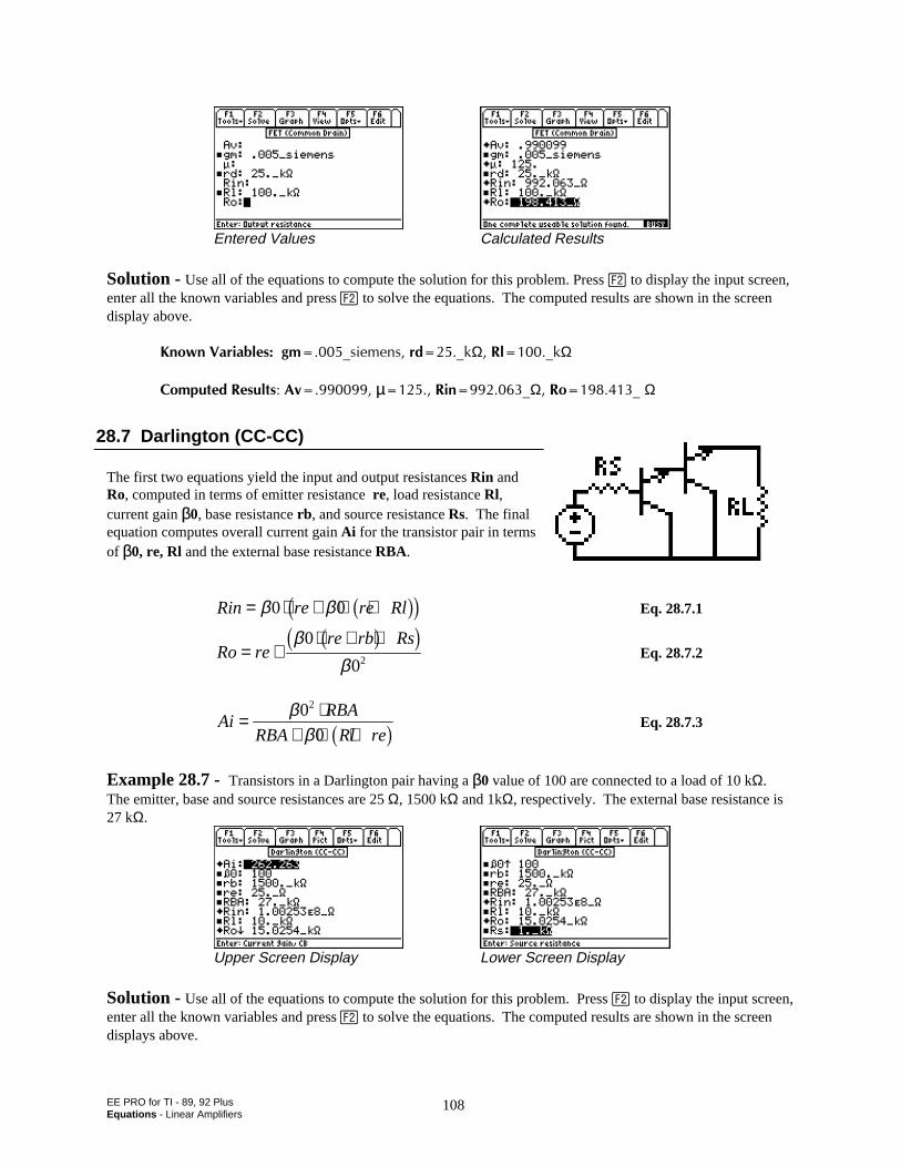
EE PRO for TI - 89, 92 PlusEquations - Linear Amplifiers
108
Entered Values Calculated Results
Solution - Use all of the equations to compute the solution for this problem. Press „ to display the input screen,enter all the known variables and press „ to solve the equations. The computed results are shown in the screendisplay above.
-PQYP8CTKCDNGUIOAUKGOGPUTFAMΩ4NAMΩ
%QORWVGF4GUWNVU#Xµµ4KPAΩ4QAΩ
28.7 Darlington (CC-CC)
The first two equations yield the input and output resistances Rin andRo, computed in terms of emitter resistance re, load resistance Rl,current gain ββ0, base resistance rb , and source resistance Rs. The finalequation computes overall current gain Ai for the transistor pair in termsof ββ0, re, Rl and the external base resistance RBA.
Rin re re Rl= ⋅ + ⋅ +β β0 0 b gc h Eq. 28.7.1
Ro rere rb Rs
= +⋅ + +β
β0
02
b gc hEq. 28.7.2
AiRBA
RBA Rl re= ⋅
+ ⋅ +β
β0
0
2
b g Eq. 28.7.3
Example 28.7 - Transistors in a Darlington pair having a ββ0 value of 100 are connected to a load of 10 kΩ.The emitter, base and source resistances are 25 Ω, 1500 kΩ and 1kΩ, respectively. The external base resistance is27 kΩ.
Upper Screen Display Lower Screen Display
Solution - Use all of the equations to compute the solution for this problem. Press „ to display the input screen,enter all the known variables and press „ to solve the equations. The computed results are shown in the screendisplays above.
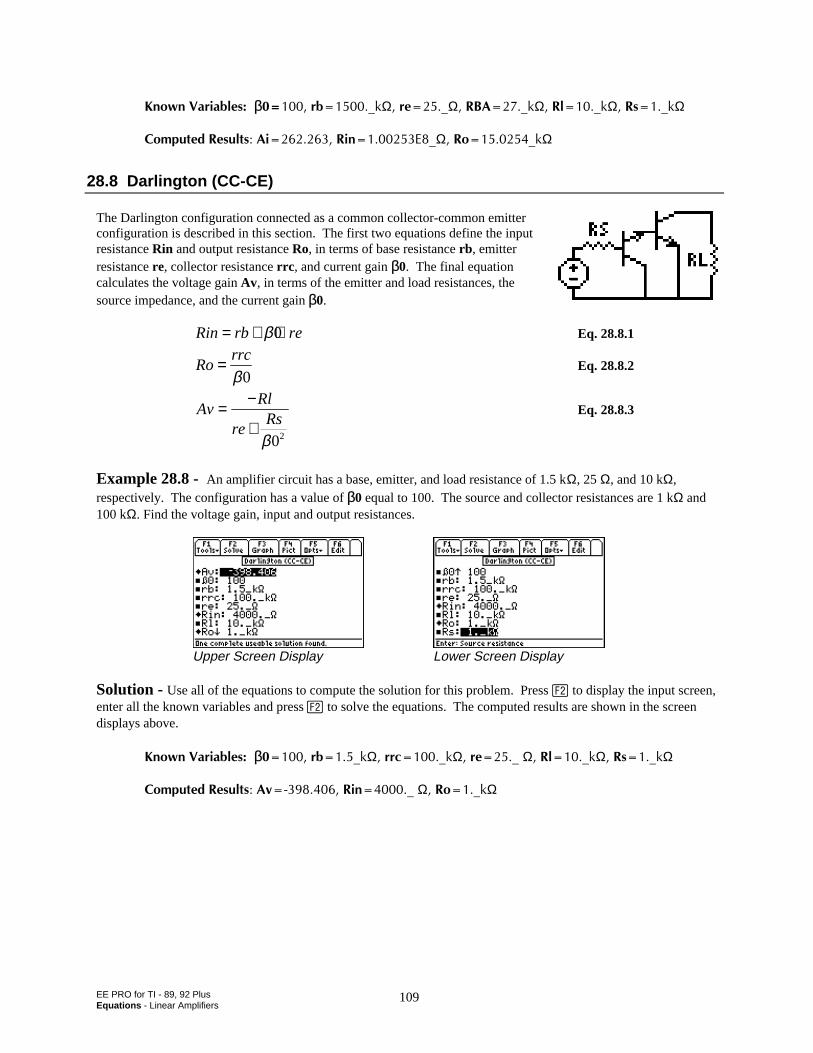
EE PRO for TI - 89, 92 PlusEquations - Linear Amplifiers
109
-PQYP8CTKCDNGUβTDAMΩTGAΩ4$#AMΩ4NAMΩ4UAMΩ
%QORWVGF4GUWNVU#K4KP'AΩ4QAMΩ
28.8 Darlington (CC-CE)
The Darlington configuration connected as a common collector-common emitterconfiguration is described in this section. The first two equations define the inputresistance Rin and output resistance Ro, in terms of base resistance rb , emitterresistance re, collector resistance rrc , and current gain ββ0. The final equationcalculates the voltage gain Av, in terms of the emitter and load resistances, thesource impedance, and the current gain ββ0.
Rin rb re= + ⋅β0 Eq. 28.8.1
Rorrc=β0
Eq. 28.8.2
AvRl
reRs
= −
+β02
Eq. 28.8.3
Example 28.8 - An amplifier circuit has a base, emitter, and load resistance of 1.5 kΩ, 25 Ω, and 10 kΩ,respectively. The configuration has a value of ββ0 equal to 100. The source and collector resistances are 1 kΩ and100 kΩ. Find the voltage gain, input and output resistances.
Upper Screen Display Lower Screen Display
Solution - Use all of the equations to compute the solution for this problem. Press „ to display the input screen,enter all the known variables and press „ to solve the equations. The computed results are shown in the screendisplays above.
-PQYP8CTKCDNGUββTDAMΩTTEAMΩTGAΩ4NAMΩ4UAMΩ
%QORWVGF4GUWNVU#X4KPAΩ4QAMΩ
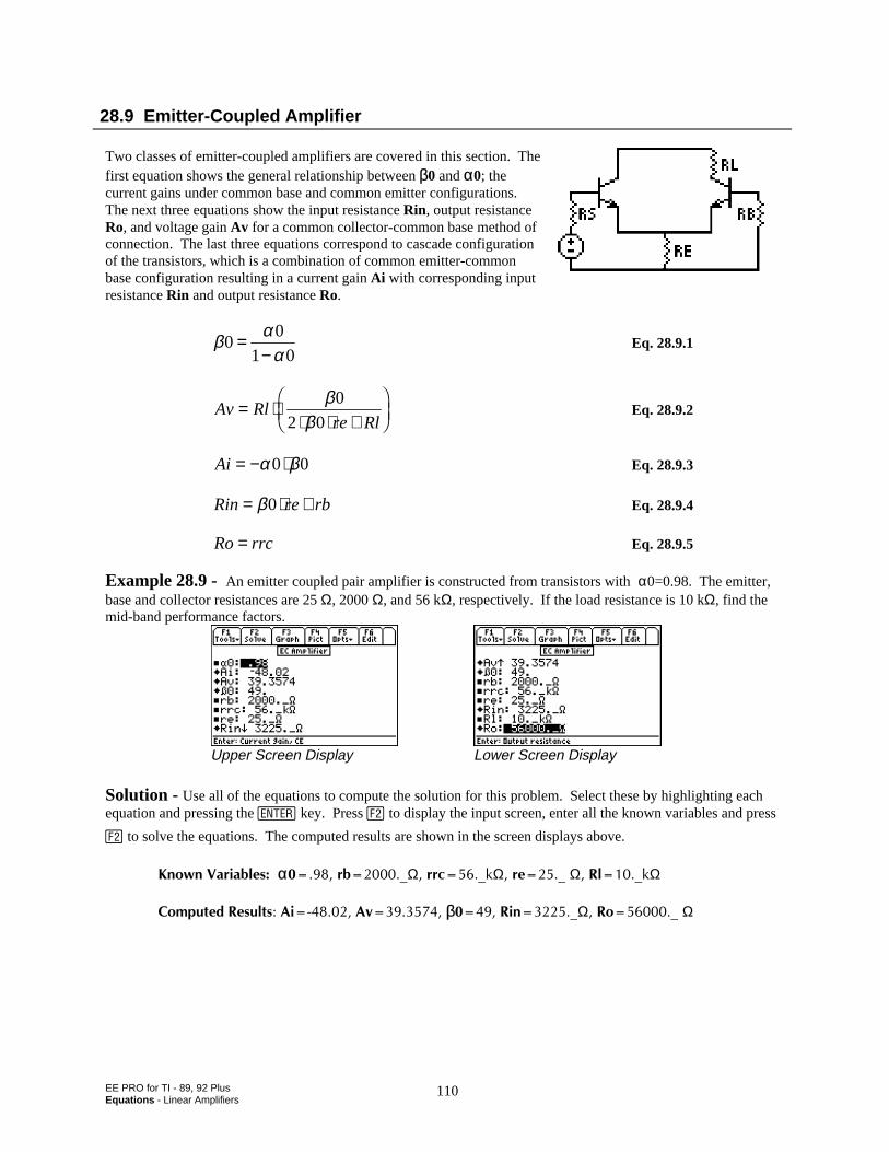
EE PRO for TI - 89, 92 PlusEquations - Linear Amplifiers
110
28.9 Emitter-Coupled Amplifier
Two classes of emitter-coupled amplifiers are covered in this section. Thefirst equation shows the general relationship between β0 and α0; thecurrent gains under common base and common emitter configurations.The next three equations show the input resistance Rin, output resistanceRo, and voltage gain Av for a common collector-common base method ofconnection. The last three equations correspond to cascade configurationof the transistors, which is a combination of common emitter-commonbase configuration resulting in a current gain Ai with corresponding inputresistance Rin and output resistance Ro.
β αα
00
1 0=
−Eq. 28.9.1
Av Rlre Rl
= ⋅⋅ ⋅ +
FHG
IKJ
ββ
0
2 0Eq. 28.9.2
Ai = − ⋅α β0 0 Eq. 28.9.3
Rin re rb= ⋅ +β0 Eq. 28.9.4
Ro rrc= Eq. 28.9.5
Example 28.9 - An emitter coupled pair amplifier is constructed from transistors with α0=0.98. The emitter,base and collector resistances are 25 Ω, 2000 Ω, and 56 kΩ, respectively. If the load resistance is 10 kΩ, find themid-band performance factors.
Upper Screen Display Lower Screen Display
Solution - Use all of the equations to compute the solution for this problem. Select these by highlighting eachequation and pressing the key. Press „ to display the input screen, enter all the known variables and press
„ to solve the equations. The computed results are shown in the screen displays above.
-PQYP8CTKCDNGUαTDAΩTTEAMΩTGAΩ4NAMΩ
%QORWVGF4GUWNVU#K#Xβ4KPAΩ4QAΩ
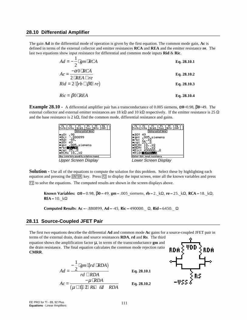
EE PRO for TI - 89, 92 PlusEquations - Linear Amplifiers
111
28.10 Differential Amplifier
The gain Ad in the differential mode of operation is given by the first equation. The common mode gain, Ac isdefined in terms of the external collector and emitter resistances RCA and REA and the emitter resistance re. Thelast two equations show input resistance for differential and common mode inputs Rid & Ric.
Ad gm RCA= − ⋅ ⋅1
2Eq. 28.10.1
AcRCA
REA re= − ⋅
⋅ +α0
2Eq. 28.10.2
Rid rb re= ⋅ + ⋅2 0βb g Eq. 28.10.3
Ric REA= ⋅β0 Eq. 28.10.4
Example 28.10 - A differential amplifier pair has a transconductance of 0.005 siemens, αα0=0.98, ββ0=49. Theexternal collector and external emitter resistances are 18 kΩ and 10 kΩ respectively. If the emitter resistance is 25 Ωand the base resistance is 2 kΩ, find the common mode, differential resistance and gains.
Upper Screen Display Lower Screen Display
Solution - Use all of the equations to compute the solution for this problem. Select these by highlighting eachequation and pressing the key. Press „ to display the input screen, enter all the known variables and press
„ to solve the equations. The computed results are shown in the screen displays above.
-PQYP8CTKCDNGUααββIOAUKGOGPUTDAMΩTGAMΩ4%#AMΩ
4'#AMΩ
%QORWVGF4GUWNVU#E#F4KEAΩ4KFAΩ
28.11 Source-Coupled JFET Pair
The first two equations describe the differential Ad and common mode Ac gains for a source-coupled JFET pair interms of the external drain, drain and source resistances RDA, rd and Rs. The thirdequation shows the amplification factor µµ, in terms of the transconductance gm andthe drain resistance. The final equation calculates the common mode rejection ratioCMRR .
Adgm rd RDA
rd RDA=
− ⋅ ⋅ ⋅
+
12
b gEq. 28.10.1
AcRDA
Rs rd RDA= − ⋅
+ ⋅ ⋅ + +µ
µ 1 2b g Eq. 28.10.2
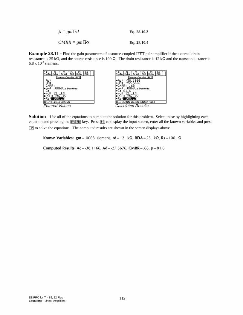
EE PRO for TI - 89, 92 PlusEquations - Linear Amplifiers
112
µ = ⋅gm rd Eq. 28.10.3
CMRR gm Rs= ⋅ Eq. 28.10.4
Example 28.11 - Find the gain parameters of a source-coupled JFET pair amplifier if the external drainresistance is 25 kΩ, and the source resistance is 100 Ω. The drain resistance is 12 kΩ and the transconductance is6.8 x 10-3 siemens.
Entered Values Calculated Results
Solution - Use all of the equations to compute the solution for this problem. Select these by highlighting eachequation and pressing the key. Press „ to display the input screen, enter all the known variables and press
„ to solve the equations. The computed results are shown in the screen displays above.
-PQYP8CTKCDNGUIOAUKGOGPUTFAMΩ4&#AMΩ4UAΩ
%QORWVGF4GUWNVU#E#F%/44µ
EE PRO for TI - 89, 92 PlusEquations - Class A, B, C Amplifiers
113
Chapter 29 Class A, B and C AmplifiersThis chapter covers the section called Class A, B and C Amplifiers. These amplifier circuits forms the basis of aclass of power amplifiers used in a variety of applications in the industry.
Read this!Note: The equations in this section are grouped under topics which describe general properties of Class A, B, and Camplifiers. Equations for a variety of specific cases and are listed together under a sub-topic heading and are notnecessarily a set of consistent equations which can be solved together. Choosing equations in a subtopic w/o regardas to whether the equations represent actual relationships could generate erroneous results or no solution at all. Readthe description of each equation set to determine which equations in a sub-topic form a consistent subset beforeattempting to compute a solution.
Class A AmplifierPower TransistorPush-Pull Principle
Class B AmplifierClass C Amplifier
Variables
The variables used in this section are listed along with a brief description and units.
Variable Description Unitgm Transconductance ShFE CE current gain unitlesshOE CE output conductance SI Current AIB Base current AIC Collector Current A∆IC Current swing from operating pt. AICBO Collector current EB open AICQ Current at operating point AIdc DC current AImax Maximum current AK Constant unitlessm Constant 1/Kς Efficiency unitlessn Turns ratio unitlessN1 # turns in primary unitlessN2 # turns in secondary unitlessPd Power dissipated WPdc DC power input to amp W
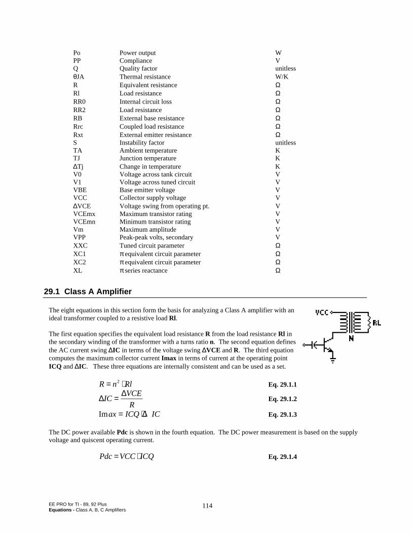
EE PRO for TI - 89, 92 PlusEquations - Class A, B, C Amplifiers
114
Po Power output WPP Compliance VQ Quality factor unitlessθJA Thermal resistance W/KR Equivalent resistance ΩRl Load resistance ΩRR0 Internal circuit loss ΩRR2 Load resistance ΩRB External base resistance ΩRrc Coupled load resistance ΩRxt External emitter resistance ΩS Instability factor unitlessTA Ambient temperature KTJ Junction temperature K∆Tj Change in temperature KV0 Voltage across tank circuit VV1 Voltage across tuned circuit VVBE Base emitter voltage VVCC Collector supply voltage V∆VCE Voltage swing from operating pt. VVCEmx Maximum transistor rating VVCEmn Minimum transistor rating VVm Maximum amplitude VVPP Peak-peak volts, secondary VXXC Tuned circuit parameter ΩXC1 π equivalent circuit parameter ΩXC2 π equivalent circuit parameter ΩXL π series reactance Ω
29.1 Class A Amplifier
The eight equations in this section form the basis for analyzing a Class A amplifier with anideal transformer coupled to a resistive load Rl.
The first equation specifies the equivalent load resistance R from the load resistance Rl inthe secondary winding of the transformer with a turns ratio n. The second equation definesthe AC current swing ∆IC in terms of the voltage swing ∆VCE and R. The third equationcomputes the maximum collector current Imax in terms of current at the operating pointICQ and ∆IC . These three equations are internally consistent and can be used as a set.
R n Rl= ⋅2 Eq. 29.1.1
∆ ∆IC
VCE
R= Eq. 29.1.2
Imax ICQ IC= + ∆ Eq. 29.1.3
The DC power available Pdc is shown in the fourth equation. The DC power measurement is based on the supplyvoltage and quiscent operating current.
Pdc VCC ICQ= ⋅ Eq. 29.1.4
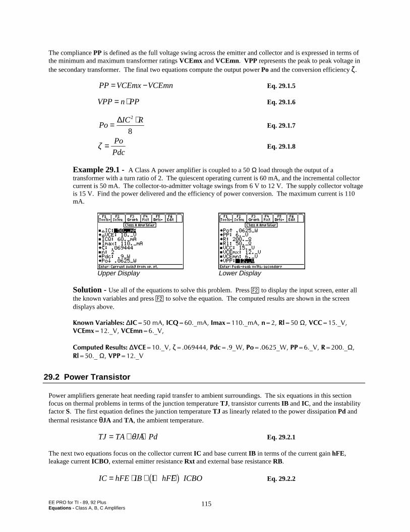
EE PRO for TI - 89, 92 PlusEquations - Class A, B, C Amplifiers
115
The compliance PP is defined as the full voltage swing across the emitter and collector and is expressed in terms ofthe minimum and maximum transformer ratings VCEmx and VCEmn. VPP represents the peak to peak voltage inthe secondary transformer. The final two equations compute the output power Po and the conversion efficiency ζ.
PP VCEmx VCEmn= − Eq. 29.1.5
VPP n PP= ⋅ Eq. 29.1.6
PoIC R= ⋅∆ 2
8Eq. 29.1.7
ζ = Po
PdcEq. 29.1.8
Example 29.1 - A Class A power amplifier is coupled to a 50 Ω load through the output of atransformer with a turn ratio of 2. The quiescent operating current is 60 mA, and the incremental collectorcurrent is 50 mA. The collector-to-admitter voltage swings from 6 V to 12 V. The supply collector voltageis 15 V. Find the power delivered and the efficiency of power conversion. The maximum current is 110mA.
Upper Display Lower Display
Solution - Use all of the equations to solve this problem. Press „ to display the input screen, enter allthe known variables and press „ to solve the equation. The computed results are shown in the screendisplays above.
-PQYP8CTKCDNGU∆+%O#+%3AO#+OCZAO#P4NΩ8%%A88%'OZA88%'OPA8
%QORWVGF4GUWNVU∆8%'A8ζ2FEA92QA922A84AΩ
4NAΩ822A8
29.2 Power Transistor
Power amplifiers generate heat needing rapid transfer to ambient surroundings. The six equations in this sectionfocus on thermal problems in terms of the junction temperature TJ, transistor currents IB and IC , and the instabilityfactor S. The first equation defines the junction temperature TJ as linearly related to the power dissipation Pd andthermal resistance θθJA and TA , the ambient temperature.
TJ TA JA Pd= + ⋅θ Eq. 29.2.1
The next two equations focus on the collector current IC and base current IB in terms of the current gain hFE,leakage current ICBO , external emitter resistance Rxt and external base resistance RB.
IC hFE IB hFE ICBO= ⋅ + + ⋅1b g Eq. 29.2.2
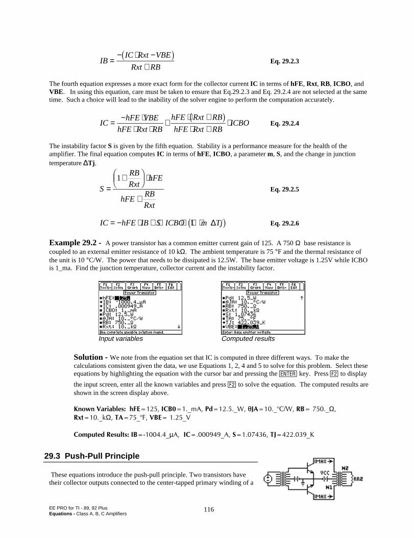
EE PRO for TI - 89, 92 PlusEquations - Class A, B, C Amplifiers
116
IBIC Rxt VBE
Rxt RB=
− ⋅ −+
b gEq. 29.2.3
The fourth equation expresses a more exact form for the collector current IC in terms of hFE, Rxt, RB, ICBO , andVBE. In using this equation, care must be taken to ensure that Eq.29.2.3 and Eq. 29.2.4 are not selected at the sametime. Such a choice will lead to the inability of the solver engine to perform the computation accurately.
IChFE VBE
hFE Rxt RB
hFE Rxt RB
hFE Rxt RBICBO= − ⋅
⋅ ⋅+
⋅ +⋅ +
⋅b gEq. 29.2.4
The instability factor S is given by the fifth equation. Stability is a performance measure for the health of theamplifier. The final equation computes IC in terms of hFE, ICBO , a parameter m, S, and the change in junctiontemperature ∆∆Tj .
S
RB
RxthFE
hFERB
Rxt
=+F
HGIKJ ⋅
+
1Eq. 29.2.5
IC hFE IB S ICBO m Tj= − ⋅ + ⋅ ⋅ + ⋅1 ∆b g Eq. 29.2.6
Example 29.2 - A power transistor has a common emitter current gain of 125. A 750 Ω base resistance iscoupled to an external emitter resistance of 10 kΩ. The ambient temperature is 75 °F and the thermal resistance ofthe unit is 10 °C/W. The power that needs to be dissipated is 12.5W. The base emitter voltage is 1.25V while ICBOis 1_ma. Find the junction temperature, collector current and the instability factor.
Input variables Computed results
Solution - We note from the equation set that IC is computed in three different ways. To make thecalculations consistent given the data, we use Equations 1, 2, 4 and 5 to solve for this problem. Select theseequations by highlighting the equation with the cursor bar and pressing the ¸ key. Press „ to display
the input screen, enter all the known variables and press „ to solve the equation. The computed results areshown in the screen display above.
-PQYP8CTKCDNGUJ('+%$AO#2FA9θ,#AQ%94$AΩ
4ZVAMΩ6#AQ(8$'A8
%QORWVGF4GUWNVU+$Aµ#+%A#56,A-
29.3 Push-Pull Principle
These equations introduce the push-pull principle. Two transistors havetheir collector outputs connected to the center-tapped primary winding of a
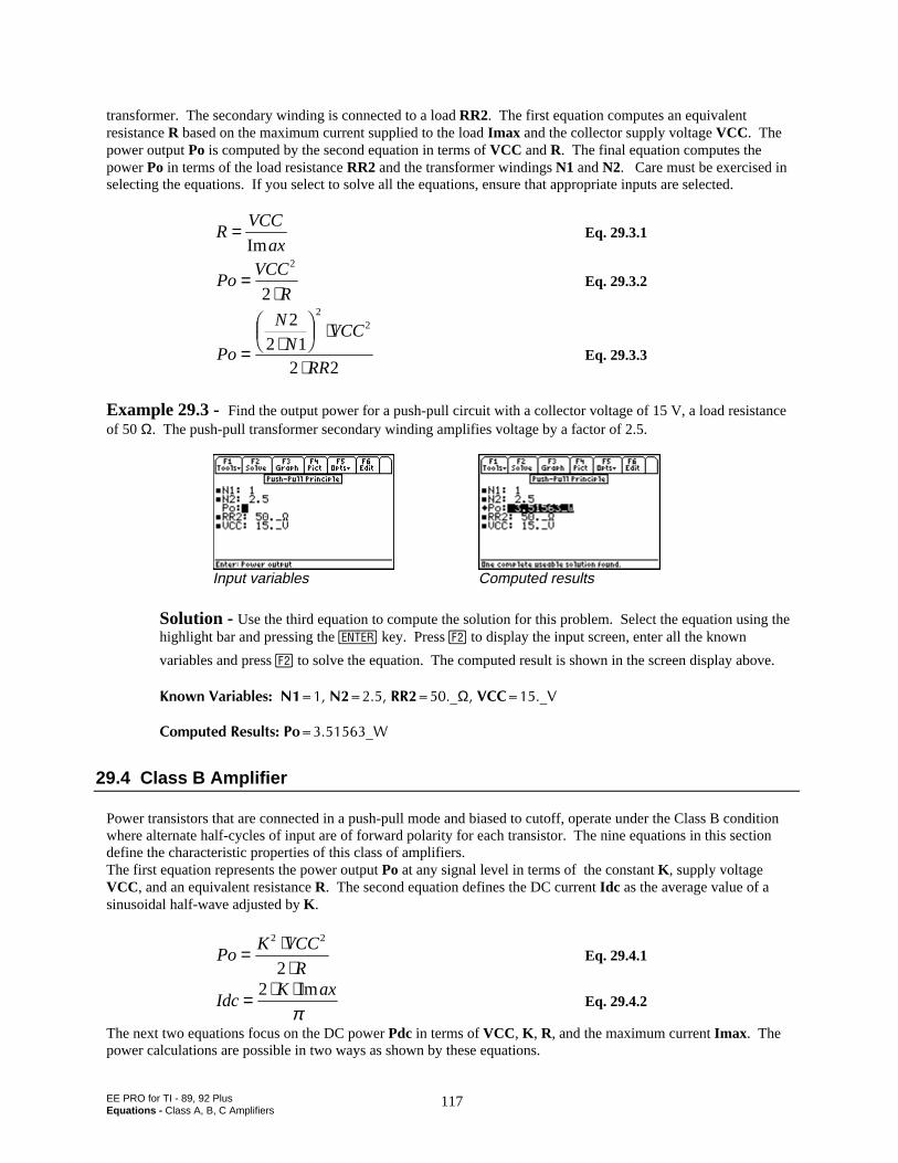
EE PRO for TI - 89, 92 PlusEquations - Class A, B, C Amplifiers
117
transformer. The secondary winding is connected to a load RR2. The first equation computes an equivalentresistance R based on the maximum current supplied to the load Imax and the collector supply voltage VCC. Thepower output Po is computed by the second equation in terms of VCC and R. The final equation computes thepower Po in terms of the load resistance RR2 and the transformer windings N1 and N2. Care must be exercised inselecting the equations. If you select to solve all the equations, ensure that appropriate inputs are selected.
RVCC
ax=
ImEq. 29.3.1
PoVCC
R=
⋅
2
2Eq. 29.3.2
Po
N
NVCC
RR= ⋅FHG
IKJ ⋅
⋅
22 1
2 2
22
Eq. 29.3.3
Example 29.3 - Find the output power for a push-pull circuit with a collector voltage of 15 V, a load resistanceof 50 Ω. The push-pull transformer secondary winding amplifies voltage by a factor of 2.5.
Input variables Computed results
Solution - Use the third equation to compute the solution for this problem. Select the equation using thehighlight bar and pressing the key. Press „ to display the input screen, enter all the known
variables and press „ to solve the equation. The computed result is shown in the screen display above.
-PQYP8CTKCDNGU0044AΩ8%%A8
%QORWVGF4GUWNVU2QA9
29.4 Class B Amplifier
Power transistors that are connected in a push-pull mode and biased to cutoff, operate under the Class B conditionwhere alternate half-cycles of input are of forward polarity for each transistor. The nine equations in this sectiondefine the characteristic properties of this class of amplifiers.The first equation represents the power output Po at any signal level in terms of the constant K , supply voltageVCC, and an equivalent resistance R. The second equation defines the DC current Idc as the average value of asinusoidal half-wave adjusted by K .
PoK VCC
R= ⋅
⋅
2 2
2Eq. 29.4.1
IdcK ax= ⋅ ⋅2 Im
πEq. 29.4.2
The next two equations focus on the DC power Pdc in terms of VCC, K , R, and the maximum current Imax. Thepower calculations are possible in two ways as shown by these equations.
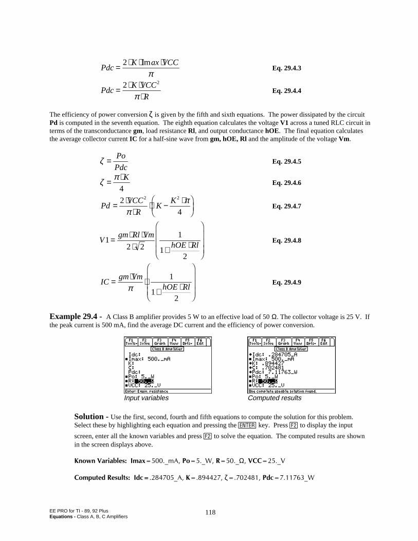
EE PRO for TI - 89, 92 PlusEquations - Class A, B, C Amplifiers
118
PdcK ax VCC= ⋅ ⋅ ⋅2 Im
πEq. 29.4.3
PdcK VCC
R= ⋅ ⋅
⋅2 2
πEq. 29.4.4
The efficiency of power conversion ζζ is given by the fifth and sixth equations. The power dissipated by the circuitPd is computed in the seventh equation. The eighth equation calculates the voltage V1 across a tuned RLC circuit interms of the transconductance gm, load resistance Rl, and output conductance hOE. The final equation calculatesthe average collector current IC for a half-sine wave from gm, hOE, Rl and the amplitude of the voltage Vm.
ζ = Po
PdcEq. 29.4.5
ζ π= ⋅ K
4Eq. 29.4.6
PdVCC
RK
K= ⋅⋅
⋅ − ⋅FHG
IKJ
2
4
2 2
ππ
Eq. 29.4.7
Vgm Rl Vm
hOE Rl1
2 2
1
12
= ⋅ ⋅⋅ + ⋅
F
HGGG
I
KJJJ
Eq. 29.4.8
ICgm Vm
hOE Rl= ⋅ ⋅
+ ⋅
F
HGGG
I
KJJJπ
1
12
Eq. 29.4.9
Example 29.4 - A Class B amplifier provides 5 W to an effective load of 50 Ω. The collector voltage is 25 V. Ifthe peak current is 500 mA, find the average DC current and the efficiency of power conversion.
Input variables Computed results
Solution - Use the first, second, fourth and fifth equations to compute the solution for this problem.Select these by highlighting each equation and pressing the key. Press „ to display the input
screen, enter all the known variables and press „ to solve the equation. The computed results are shownin the screen displays above.
-PQYP8CTKCDNGU+OCZAO#2QA94AΩ8%%A8
%QORWVGF4GUWNVU+FEA#-ζ2FEA9
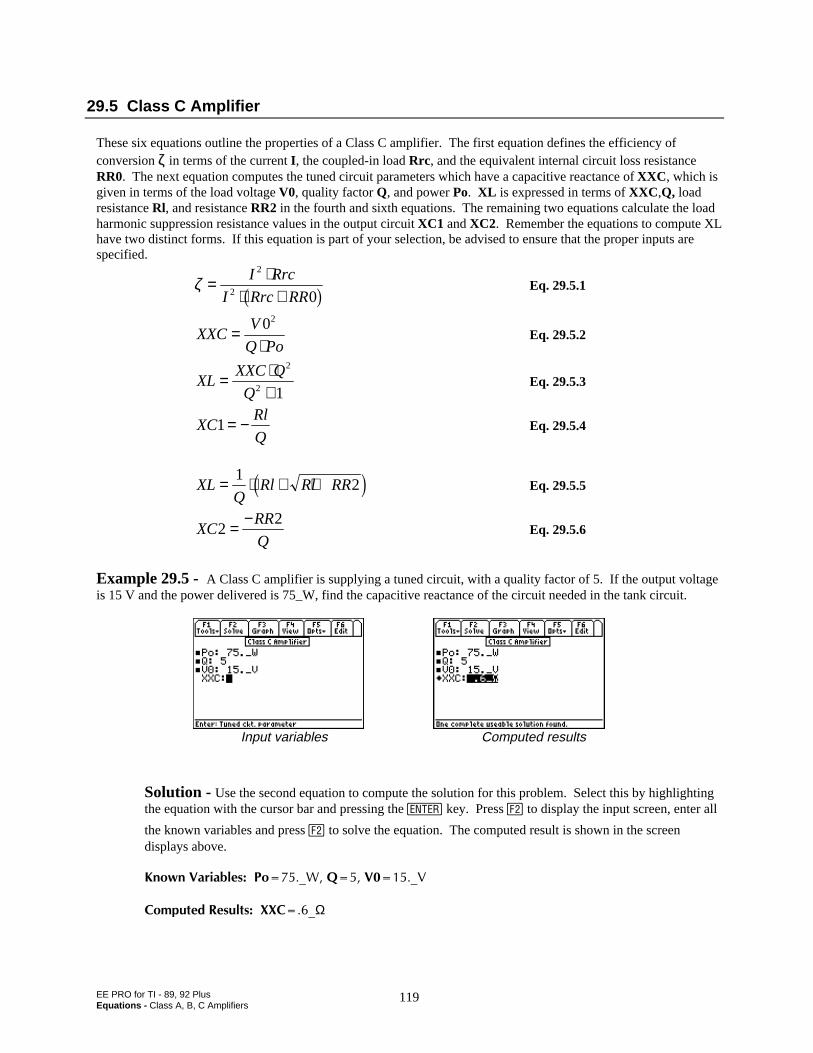
EE PRO for TI - 89, 92 PlusEquations - Class A, B, C Amplifiers
119
29.5 Class C Amplifier
These six equations outline the properties of a Class C amplifier. The first equation defines the efficiency ofconversion ζ in terms of the current I , the coupled-in load Rrc, and the equivalent internal circuit loss resistanceRR0. The next equation computes the tuned circuit parameters which have a capacitive reactance of XXC , which isgiven in terms of the load voltage V0, quality factor Q, and power Po. XL is expressed in terms of XXC ,Q, loadresistance Rl, and resistance RR2 in the fourth and sixth equations. The remaining two equations calculate the loadharmonic suppression resistance values in the output circuit XC1 and XC2. Remember the equations to compute XLhave two distinct forms. If this equation is part of your selection, be advised to ensure that the proper inputs arespecified.
ζ = ⋅⋅ +
I Rrc
I Rrc RR
2
2 0b g Eq. 29.5.1
XXCV
Q Po=
⋅02
Eq. 29.5.2
XLXXC Q
Q= ⋅
+
2
2 1Eq. 29.5.3
XCRl
Q1= − Eq. 29.5.4
XLQ
Rl Rl RR= ⋅ + +12d i Eq. 29.5.5
XCRR
Q2
2= −Eq. 29.5.6
Example 29.5 - A Class C amplifier is supplying a tuned circuit, with a quality factor of 5. If the output voltageis 15 V and the power delivered is 75_W, find the capacitive reactance of the circuit needed in the tank circuit.
Input variables Computed results
Solution - Use the second equation to compute the solution for this problem. Select this by highlightingthe equation with the cursor bar and pressing the key. Press „ to display the input screen, enter all
the known variables and press „ to solve the equation. The computed result is shown in the screendisplays above.
-PQYP8CTKCDNGU2QA938A8
%QORWVGF4GUWNVU::%AΩ
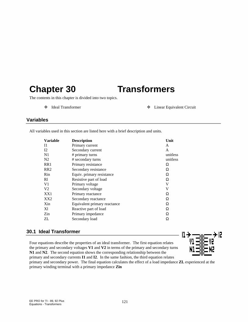
EE PRO for TI - 89, 92 PlusEquations - Transformers
121
Chapter 30 TransformersThe contents in this chapter is divided into two topics.
Ideal Transformer Linear Equivalent Circuit
Variables
All variables used in this section are listed here with a brief description and units.
Variable Description UnitI1 Primary current AI2 Secondary current AN1 # primary turns unitlessN2 # secondary turns unitlessRR1 Primary resistance ΩRR2 Secondary resistance ΩRin Equiv. primary resistance ΩRl Resistive part of load ΩV1 Primary voltage VV2 Secondary voltage VXX1 Primary reactance ΩXX2 Secondary reactance ΩXin Equivalent primary reactance ΩXl Reactive part of load ΩZin Primary impedance ΩZL Secondary load Ω
30.1 Ideal Transformer
Four equations describe the properties of an ideal transformer. The first equation relatesthe primary and secondary voltages V1 and V2 in terms of the primary and secondary turnsN1 and N2. The second equation shows the corresponding relationship between theprimary and secondary currents I1 and I2. In the same fashion, the third equation relatesprimary and secondary power. The final equation calculates the effect of a load impedance ZL experienced at theprimary winding terminal with a primary impedance Zin
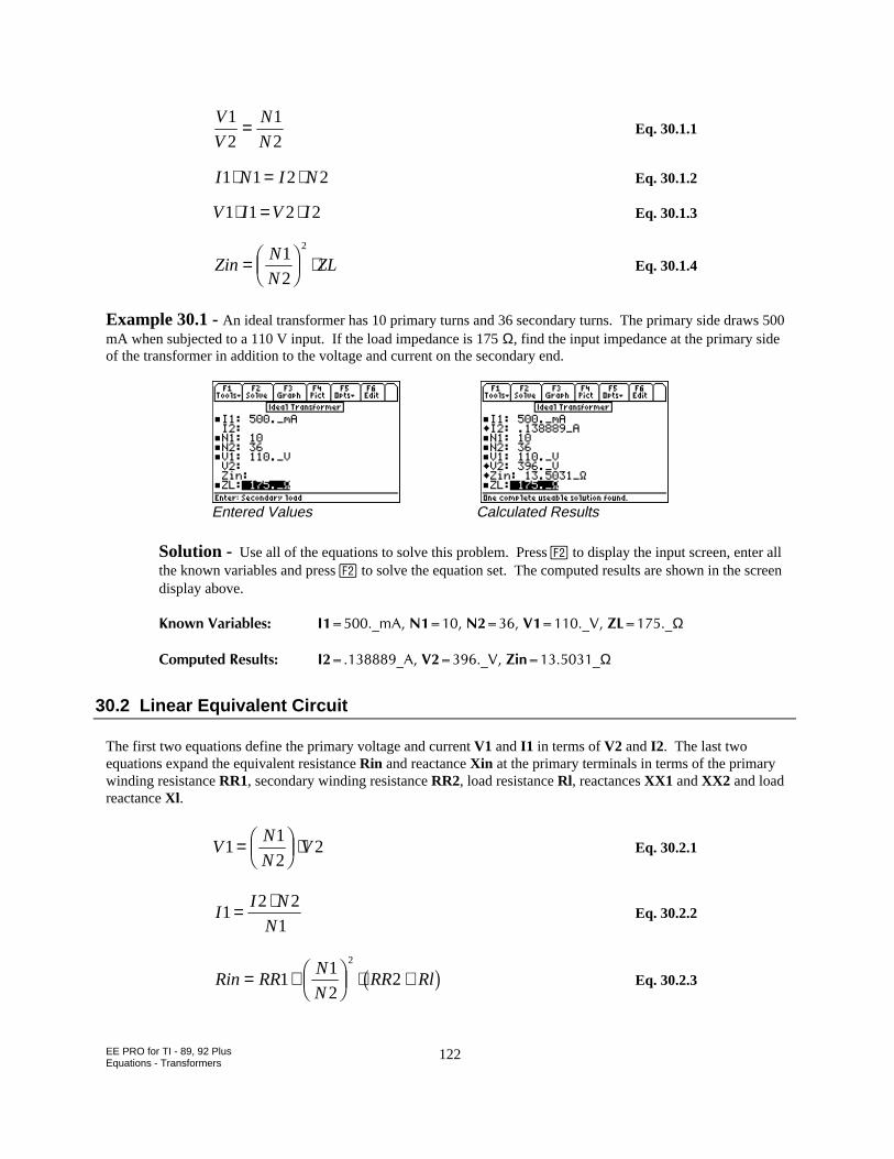
EE PRO for TI - 89, 92 PlusEquations - Transformers
122
V
V
N
N
1
2
1
2= Eq. 30.1.1
I N I N1 1 2 2⋅ = ⋅ Eq. 30.1.2
V I V I1 1 2 2⋅ = ⋅ Eq. 30.1.3
ZinN
NZL= F
HGIKJ ⋅1
2
2
Eq. 30.1.4
Example 30.1 - An ideal transformer has 10 primary turns and 36 secondary turns. The primary side draws 500mA when subjected to a 110 V input. If the load impedance is 175 Ω, find the input impedance at the primary sideof the transformer in addition to the voltage and current on the secondary end.
Entered Values Calculated Results
Solution - Use all of the equations to solve this problem. Press „ to display the input screen, enter allthe known variables and press „ to solve the equation set. The computed results are shown in the screendisplay above.
-PQYP8CTKCDNGU +AO#008A8<.AΩ
%QORWVGF4GUWNVU +A#8A8<KPAΩ
30.2 Linear Equivalent Circuit
The first two equations define the primary voltage and current V1 and I1 in terms of V2 and I2. The last twoequations expand the equivalent resistance Rin and reactance Xin at the primary terminals in terms of the primarywinding resistance RR1, secondary winding resistance RR2, load resistance Rl, reactances XX1 and XX2 and loadreactance Xl .
VN
NV1
1
22= F
HGIKJ ⋅ Eq. 30.2.1
II N
N1
2 2
1= ⋅
Eq. 30.2.2
Rin RRN
NRR Rl= + F
HGIKJ ⋅ +1
1
22
2
b g Eq. 30.2.3
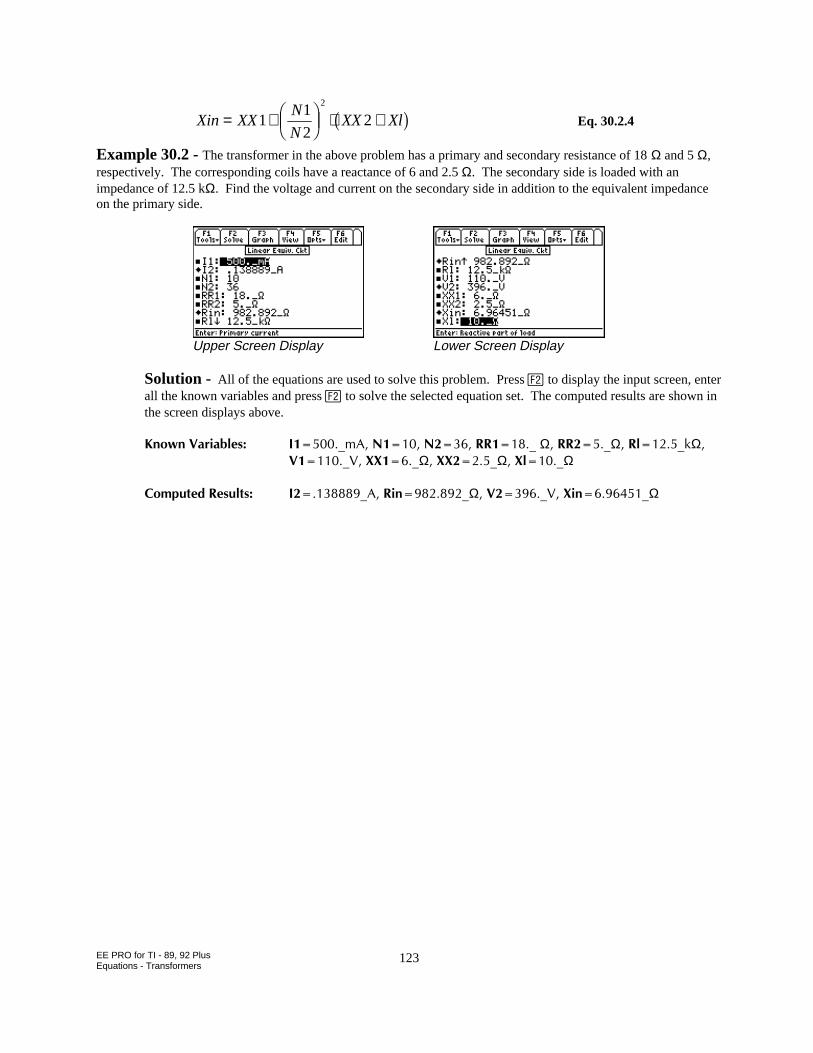
EE PRO for TI - 89, 92 PlusEquations - Transformers
123
Xin XXN
NXX Xl= + F
HGIKJ ⋅ +1
1
22
2
b g Eq. 30.2.4
Example 30.2 - The transformer in the above problem has a primary and secondary resistance of 18 Ω and 5 Ω,respectively. The corresponding coils have a reactance of 6 and 2.5 Ω. The secondary side is loaded with animpedance of 12.5 kΩ. Find the voltage and current on the secondary side in addition to the equivalent impedanceon the primary side.
Upper Screen Display Lower Screen Display
Solution - All of the equations are used to solve this problem. Press „ to display the input screen, enterall the known variables and press „ to solve the selected equation set. The computed results are shown inthe screen displays above.
-PQYP8CTKCDNGU +AO#0044AΩ44AΩ4NAMΩ
8A8::AΩ::AΩ:NAΩ
%QORWVGF4GUWNVU +A#4KPAΩ8A8:KPAΩ
EE Pro for TI-89, 92 PlusEquations - Motors and Generators
124
Chapter 31 Motors and GeneratorsThis section has thirteen topics covering various aspects of motors and generators. The topics are organized underthese headings.
Read this!Note: The equations in this section are grouped under topics which describe general properties of semiconductors ordevices. Equations for a variety of specific cases and are listed together under a sub-topic heading and are notnecessarily a set of consistent equations which can be solved together. Choosing equations in a subtopic w/o regardas to whether the equations represent actual relationships could generate erroneous results or no solution at all. Readthe description of each equation set to determine which equations in a sub-topic form a consistent subset beforeattempting to compute a solution.
Energy ConversionDC GeneratorSeparately-Excited DC GeneratorDC Shunt GeneratorDC Series GeneratorSeparately-Excited DC MotorDC Shunt Motor
DC Series MotorPermanent Magnet MotorInduction Motor IInduction Motor IISingle-Phase Induction MotorSynchronous Machines
Variables
All the variables used in this section are listed with a brief description and units.
Variable Description Unit
A Area m2
ap # parallel paths unitlessB Magnetic induction TEa Average emf induced in armature VEf Field voltage VEma Phase voltage VEs Induced voltage VEta Average emf induced per turn VF Magnetic pressure PaH Magnetic field intensity A/mIa Armature current AIIf Field current AIL Load current AIr Rotor current per phase A

EE Pro for TI-89, 92 PlusEquations - Motors and Generators
125
Isb Backward stator current AIsf Forward stator current AK Machine constant unitlessKf Field coefficient A/WbKM Induction motor constant unitlessL Length of each turn mθ Phase delay rN Total # armature coils unitlessNs # stator coils unitlessρ Resistivity Ω/mφ Flux Wbp # poles unitlessP Power WPa Mechanical power WPma Power in rotor per phase WPme Mechanical power WPr Rotor power per phase WRR1 Rotor resistance per phase ΩRa Armature resistance ΩRd Adjustable resistance ΩRe Ext. shunt resistance ΩRel Magnetic reluctance A/WbRf Field coil resistance ΩRl Load resistance ΩRr Equivalent rotor resistance ΩRs Series field resistance ΩRst Stator resistance Ωs Slip unitlesssf Slip for forward flux unitlesssm Maximum slip unitlessT Internal torque N*mTb Backward torque N*mTf Forward torque N*mTgmax Breakdown torque N*mTL Load torque N*mTloss Torque loss N*mTmmax Maximum positive torque N*mTTmax Pullout torque N*mTs Shaft torque N*mVa Applied voltage VVf Field voltage VVfs Field voltage VVt Terminal voltage Vωm Mechanical radian frequency r/sωme Electrical radian frequency r/sωr Electrical rotor speed r/sωs Electrical stator speed r/sWf Magnetic energy JXL Inductive reactance Ω
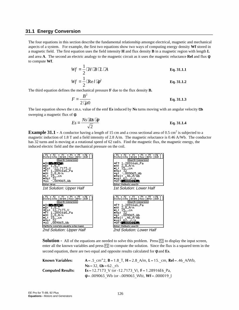
EE Pro for TI-89, 92 PlusEquations - Motors and Generators
126
31.1 Energy Conversion
The four equations in this section describe the fundamental relationship amongst electrical, magnetic and mechanicalaspects of a system. For example, the first two equations show two ways of computing energy density Wf stored ina magnetic field. The first equation uses the field intensity H and flux density B in a magnetic region with length Land area A. The second an electric analogy to the magnetic circuit as it uses the magnetic reluctance Rel and flux φto compute Wf .
Wf H B L A= ⋅ ⋅ ⋅ ⋅1
2Eq. 31.1.1
Wf l= ⋅ ⋅1
22Re φ Eq. 31.1.2
The third equation defines the mechanical pressure F due to the flux density B.
FB=⋅
2
2 0µEq. 31.1.3
The last equation shows the r.m.s. value of the emf Es induced by Ns turns moving with an angular velocity ωssweeping a magnetic flux of φ.
EsNs s= ⋅ ⋅ω φ
2Eq. 31.1.4
Example 31.1 - A conductor having a length of 15 cm and a cross sectional area of 0.5 cm2 is subjected to amagnetic induction of 1.8 T and a field intensity of 2.8 A/m. The magnetic reluctance is 0.46 A/Wb. The conductorhas 32 turns and is moving at a rotational speed of 62 rad/s. Find the magnetic flux, the magnetic energy, theinduced electric field and the mechanical pressure on the coil.
1st Solution: Upper Half 1st Solution: Lower Half
2nd Solution: Upper Half 2nd Solution: Lower Half
Solution - All of the equations are needed to solve this problem. Press „ to display the input screen,enter all the known variables and press „ to compute the solution. Since the flux is a squared term in the
second equation, there are two equal and opposite results calculated for φ and Es.
-PQYP8CTKCDNGU #AEO@$A6*A#O.AEO4GNA#9D
0UωUATU%QORWVGF4GUWNVU 'UA8QTA8('A2C
φA9DQTA9D9HA,
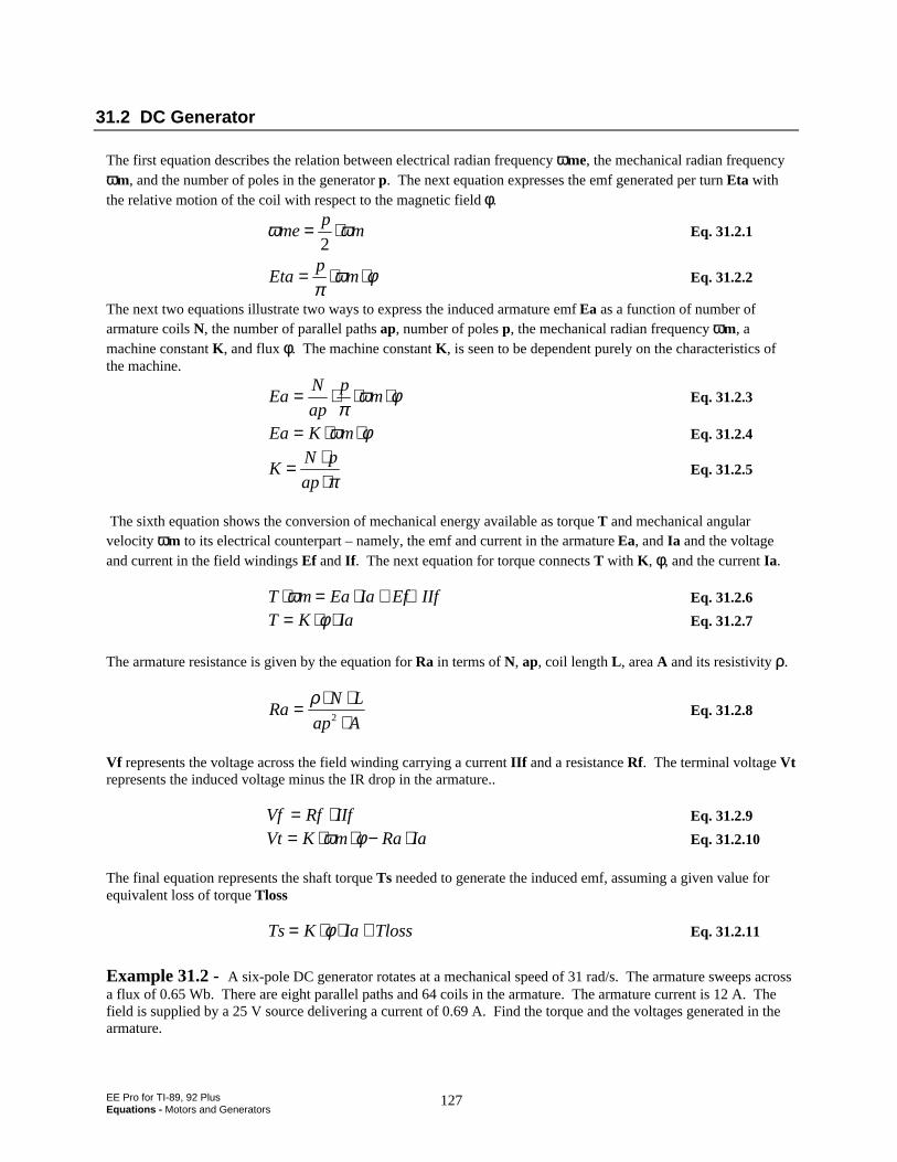
EE Pro for TI-89, 92 PlusEquations - Motors and Generators
127
31.2 DC Generator
The first equation describes the relation between electrical radian frequency ωme, the mechanical radian frequencyωm, and the number of poles in the generator p. The next equation expresses the emf generated per turn Eta withthe relative motion of the coil with respect to the magnetic field φ.
ω ωmep
m= ⋅2
Eq. 31.2.1
Etap
m= ⋅ ⋅π
ω φ Eq. 31.2.2
The next two equations illustrate two ways to express the induced armature emf Ea as a function of number ofarmature coils N, the number of parallel paths ap, number of poles p, the mechanical radian frequency ωm, amachine constant K , and flux φ. The machine constant K , is seen to be dependent purely on the characteristics ofthe machine.
EaN
ap
pm= ⋅ ⋅ ⋅
πω φ Eq. 31.2.3
Ea K m= ⋅ ⋅ω φ Eq. 31.2.4
KN p
ap= ⋅
⋅πEq. 31.2.5
The sixth equation shows the conversion of mechanical energy available as torque T and mechanical angularvelocity ωm to its electrical counterpart – namely, the emf and current in the armature Ea, and Ia and the voltageand current in the field windings Ef and If . The next equation for torque connects T with K , φ, and the current Ia.
T m Ea Ia Ef IIf⋅ = ⋅ + ⋅ω Eq. 31.2.6
T K Ia= ⋅ ⋅φ Eq. 31.2.7
The armature resistance is given by the equation for Ra in terms of N, ap, coil length L , area A and its resistivity ρ.
RaN L
ap A= ⋅ ⋅
⋅ρ
2Eq. 31.2.8
Vf represents the voltage across the field winding carrying a current IIf and a resistance Rf. The terminal voltage Vtrepresents the induced voltage minus the IR drop in the armature..
Vf Rf IIf= ⋅ Eq. 31.2.9
Vt K m Ra Ia= ⋅ ⋅ − ⋅ω φ Eq. 31.2.10
The final equation represents the shaft torque Ts needed to generate the induced emf, assuming a given value forequivalent loss of torque Tloss
Ts K Ia Tloss= ⋅ ⋅ +φ Eq. 31.2.11
Example 31.2 - A six-pole DC generator rotates at a mechanical speed of 31 rad/s. The armature sweeps acrossa flux of 0.65 Wb. There are eight parallel paths and 64 coils in the armature. The armature current is 12 A. Thefield is supplied by a 25 V source delivering a current of 0.69 A. Find the torque and the voltages generated in thearmature.
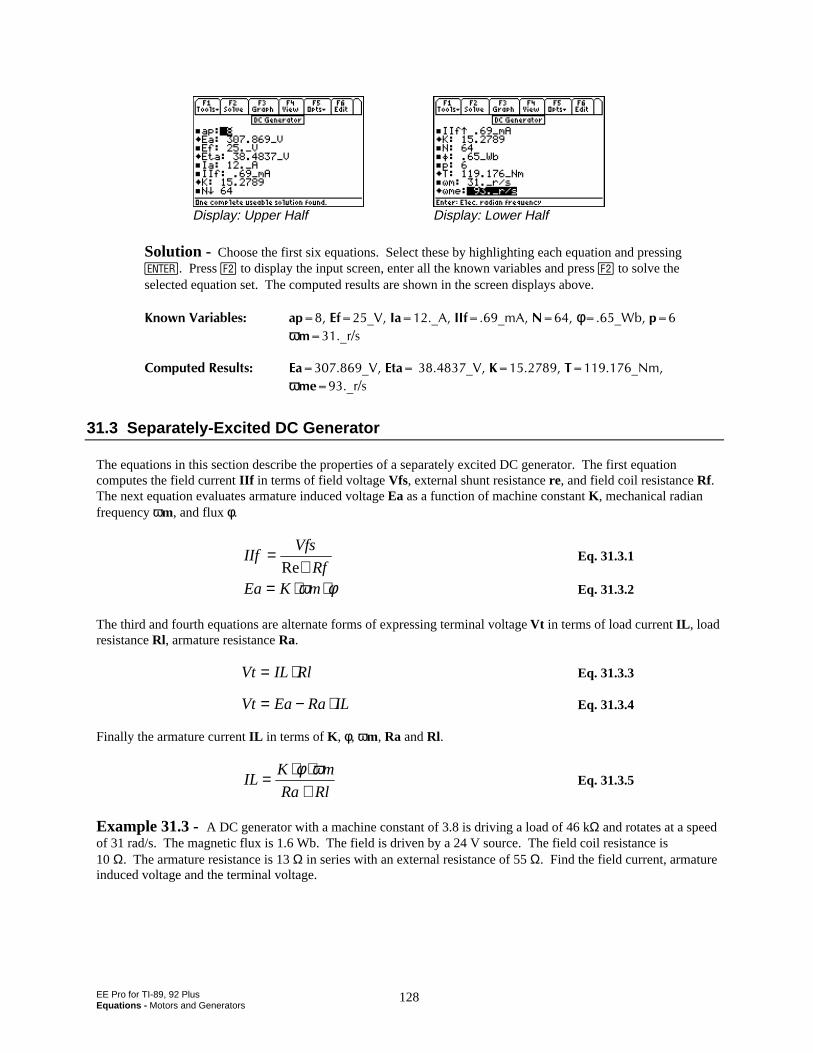
EE Pro for TI-89, 92 PlusEquations - Motors and Generators
128
Display: Upper Half Display: Lower Half
Solution - Choose the first six equations. Select these by highlighting each equation and pressing¸. Press „ to display the input screen, enter all the known variables and press „ to solve theselected equation set. The computed results are shown in the screen displays above.
-PQYP8CTKCDNGU CR'HA8+CA#++HAO#0φA9DR
ωOATU
%QORWVGF4GUWNVU 'CA8'VCA8-6A0O
ωOGATU
31.3 Separately-Excited DC Generator
The equations in this section describe the properties of a separately excited DC generator. The first equationcomputes the field current IIf in terms of field voltage Vfs, external shunt resistance re, and field coil resistance Rf.The next equation evaluates armature induced voltage Ea as a function of machine constant K , mechanical radianfrequency ωm, and flux φ.
IIfVfs
Rf=
+ReEq. 31.3.1
Ea K m= ⋅ ⋅ω φ Eq. 31.3.2
The third and fourth equations are alternate forms of expressing terminal voltage Vt in terms of load current IL , loadresistance Rl, armature resistance Ra.
Vt IL Rl= ⋅ Eq. 31.3.3
Vt Ea Ra IL= − ⋅ Eq. 31.3.4
Finally the armature current IL in terms of K , φ, ωm, Ra and Rl.
ILK m
Ra Rl= ⋅ ⋅
+φ ω
Eq. 31.3.5
Example 31.3 - A DC generator with a machine constant of 3.8 is driving a load of 46 kΩ and rotates at a speedof 31 rad/s. The magnetic flux is 1.6 Wb. The field is driven by a 24 V source. The field coil resistance is10 Ω. The armature resistance is 13 Ω in series with an external resistance of 55 Ω. Find the field current, armatureinduced voltage and the terminal voltage.
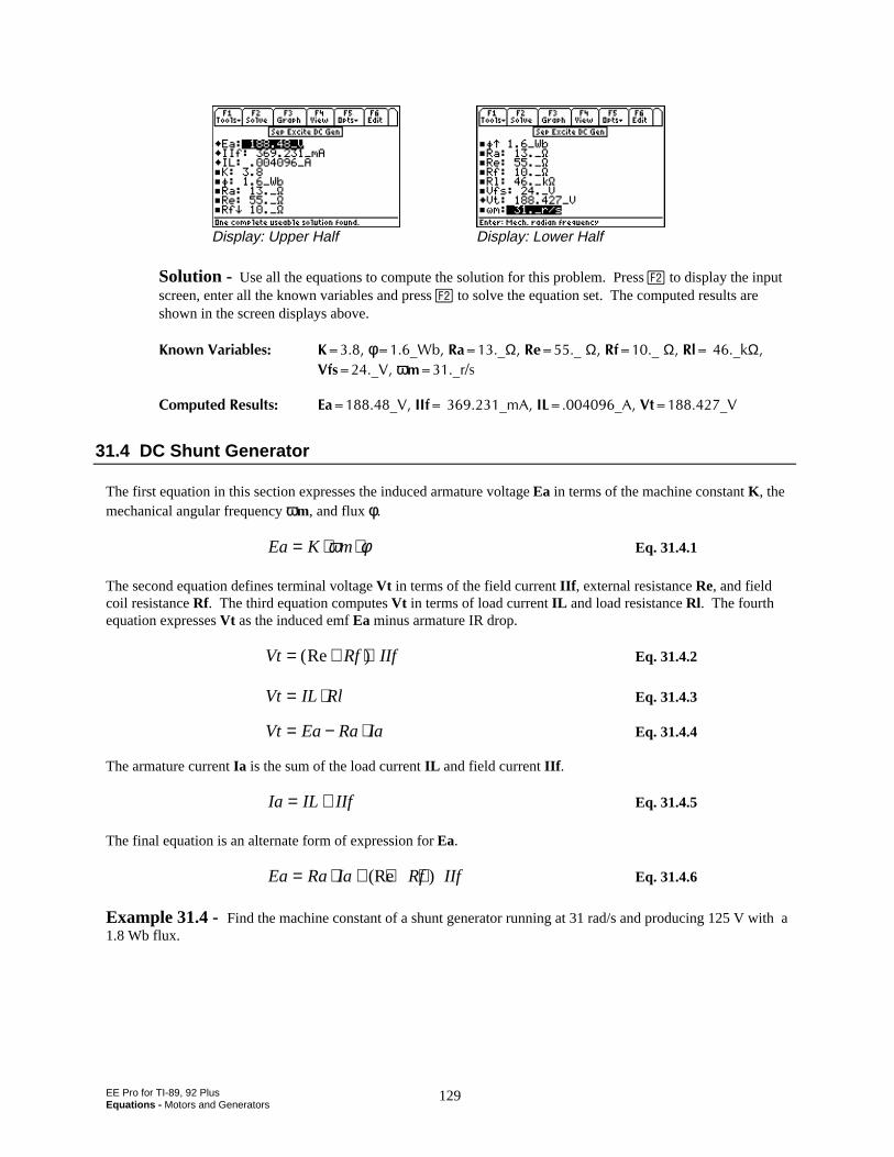
EE Pro for TI-89, 92 PlusEquations - Motors and Generators
129
Display: Upper Half Display: Lower Half
Solution - Use all the equations to compute the solution for this problem. Press „ to display the inputscreen, enter all the known variables and press „ to solve the equation set. The computed results areshown in the screen displays above.
-PQYP8CTKCDNGU -φA9D4CAΩ4GAΩ4HAΩ4NAMΩ
8HUA8ωωOATU
%QORWVGF4GUWNVU 'CA8++HAO#+.A#8VA8
31.4 DC Shunt Generator
The first equation in this section expresses the induced armature voltage Ea in terms of the machine constant K , themechanical angular frequency ωωm, and flux φφ.
Ea K m= ⋅ ⋅ω φ Eq. 31.4.1
The second equation defines terminal voltage Vt in terms of the field current IIf , external resistance Re, and fieldcoil resistance Rf. The third equation computes Vt in terms of load current IL and load resistance Rl. The fourthequation expresses Vt as the induced emf Ea minus armature IR drop.
Vt Rf IIf= + ⋅( )Re Eq. 31.4.2
Vt IL Rl= ⋅ Eq. 31.4.3
Vt Ea Ra Ia= − ⋅ Eq. 31.4.4
The armature current Ia is the sum of the load current IL and field current IIf .
Ia IL IIf= + Eq. 31.4.5
The final equation is an alternate form of expression for Ea.
Ea Ra Ia Rf IIf= ⋅ + + ⋅(Re ) Eq. 31.4.6
Example 31.4 - Find the machine constant of a shunt generator running at 31 rad/s and producing 125 V with a1.8 Wb flux.
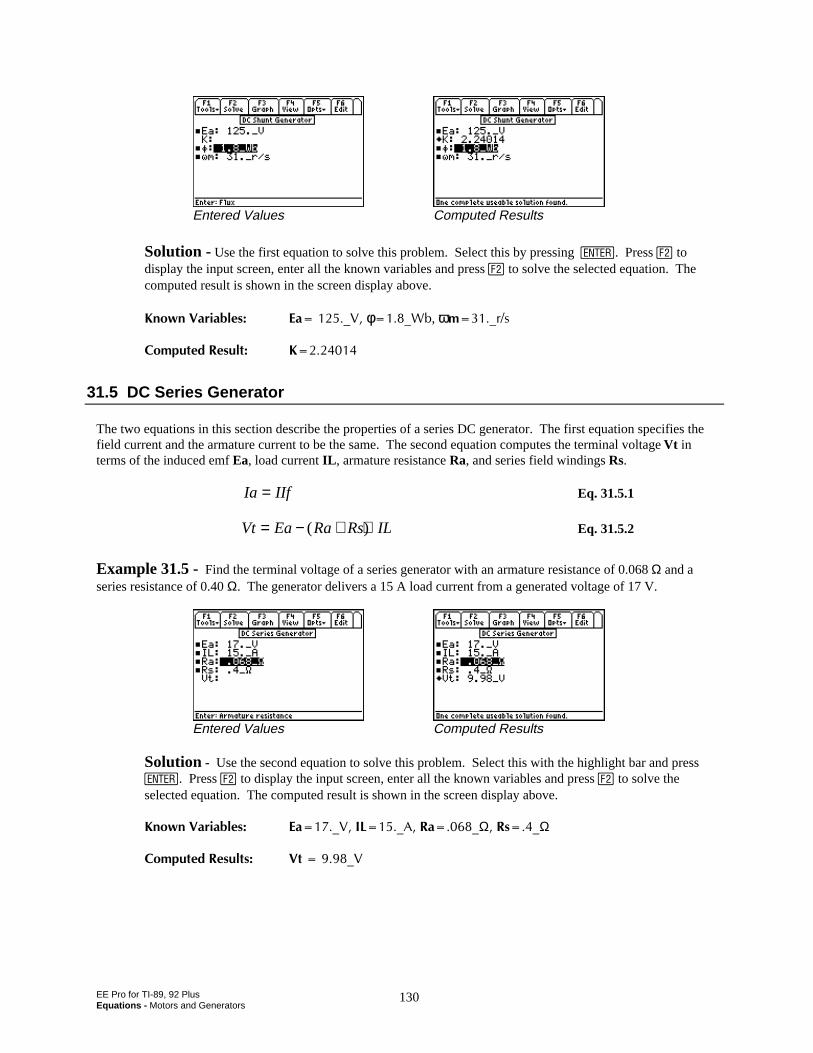
EE Pro for TI-89, 92 PlusEquations - Motors and Generators
130
Entered Values Computed Results
Solution - Use the first equation to solve this problem. Select this by pressing ¸. Press „ todisplay the input screen, enter all the known variables and press „ to solve the selected equation. Thecomputed result is shown in the screen display above.
-PQYP8CTKCDNGU 'CA8φA9D, ωOATU
%QORWVGF4GUWNV -
31.5 DC Series Generator
The two equations in this section describe the properties of a series DC generator. The first equation specifies thefield current and the armature current to be the same. The second equation computes the terminal voltage Vt interms of the induced emf Ea, load current IL , armature resistance Ra, and series field windings Rs.
Ia IIf= Eq. 31.5.1
Vt Ea Ra Rs IL= − + ⋅( ) Eq. 31.5.2
Example 31.5 - Find the terminal voltage of a series generator with an armature resistance of 0.068 Ω and aseries resistance of 0.40 Ω. The generator delivers a 15 A load current from a generated voltage of 17 V.
Entered Values Computed Results
Solution - Use the second equation to solve this problem. Select this with the highlight bar and press¸. Press „ to display the input screen, enter all the known variables and press „ to solve theselected equation. The computed result is shown in the screen display above.
-PQYP8CTKCDNGU 'CA8+.A#4CAΩ4UAΩ
%QORWVGF4GUWNVU 8VA8
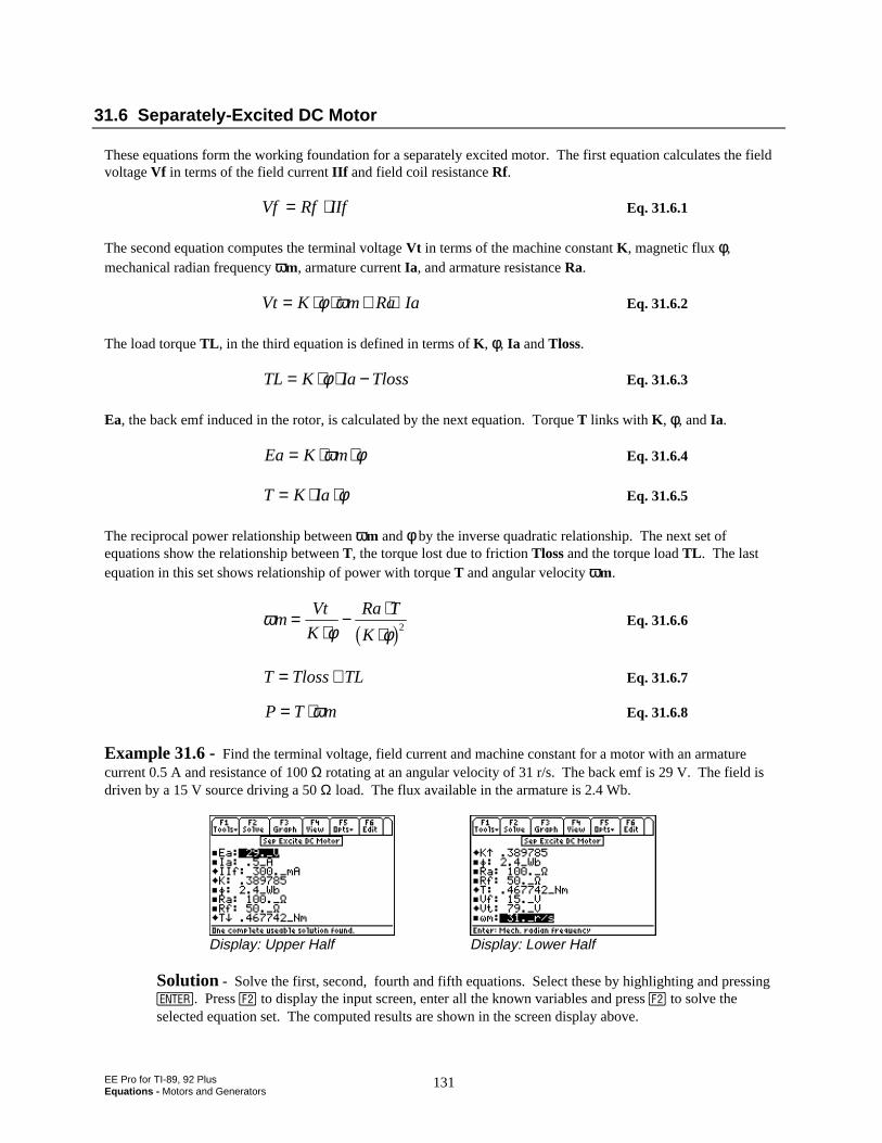
EE Pro for TI-89, 92 PlusEquations - Motors and Generators
131
31.6 Separately-Excited DC Motor
These equations form the working foundation for a separately excited motor. The first equation calculates the fieldvoltage Vf in terms of the field current IIf and field coil resistance Rf.
Vf Rf IIf= ⋅ Eq. 31.6.1
The second equation computes the terminal voltage Vt in terms of the machine constant K , magnetic flux φφ,mechanical radian frequency ωωm, armature current Ia, and armature resistance Ra.
Vt K m Ra Ia= ⋅ ⋅ + ⋅φ ω Eq. 31.6.2
The load torque TL , in the third equation is defined in terms of K , φφ, Ia and Tloss.
TL K Ia Tloss= ⋅ ⋅ −φ Eq. 31.6.3
Ea, the back emf induced in the rotor, is calculated by the next equation. Torque T links with K , φφ, and Ia.
Ea K m= ⋅ ⋅ω φ Eq. 31.6.4
T K Ia= ⋅ ⋅φ Eq. 31.6.5
The reciprocal power relationship between ωωm and φφ by the inverse quadratic relationship. The next set ofequations show the relationship between T, the torque lost due to friction Tloss and the torque load TL . The lastequation in this set shows relationship of power with torque T and angular velocity ωωm.
ωφ φ
mVt
K
Ra T
K=
⋅− ⋅
⋅b g2 Eq. 31.6.6
T Tloss TL= + Eq. 31.6.7
P T m= ⋅ω Eq. 31.6.8
Example 31.6 - Find the terminal voltage, field current and machine constant for a motor with an armaturecurrent 0.5 A and resistance of 100 Ω rotating at an angular velocity of 31 r/s. The back emf is 29 V. The field isdriven by a 15 V source driving a 50 Ωload. The flux available in the armature is 2.4 Wb.
Display: Upper Half Display: Lower Half
Solution - Solve the first, second, fourth and fifth equations. Select these by highlighting and pressing¸. Press „ to display the input screen, enter all the known variables and press „ to solve theselected equation set. The computed results are shown in the screen display above.
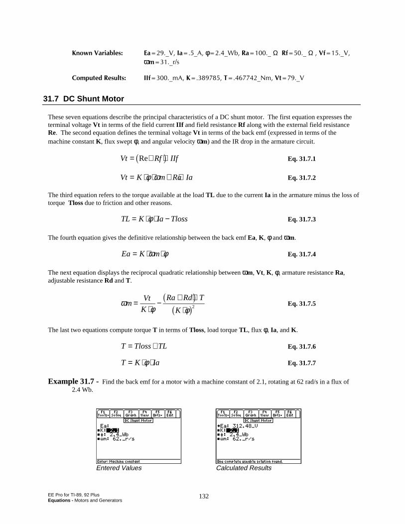
EE Pro for TI-89, 92 PlusEquations - Motors and Generators
132
-PQYP8CTKCDNGU 'CA8+CA#φA9D4CAΩ4HAΩ8HA8
ωωOATU
%QORWVGF4GUWNVU ++HAO#-6A0O8VA8
31.7 DC Shunt Motor
These seven equations describe the principal characteristics of a DC shunt motor. The first equation expresses theterminal voltage Vt in terms of the field current IIf and field resistance Rf along with the external field resistanceRe. The second equation defines the terminal voltage Vt in terms of the back emf (expressed in terms of themachine constant K , flux swept φ, and angular velocity ωm) and the IR drop in the armature circuit.
Vt Rf IIf= + ⋅Reb g Eq. 31.7.1
Vt K m Ra Ia= ⋅ ⋅ + ⋅φ ω Eq. 31.7.2
The third equation refers to the torque available at the load TL due to the current Ia in the armature minus the loss oftorque Tloss due to friction and other reasons.
TL K Ia Tloss= ⋅ ⋅ −φ Eq. 31.7.3
The fourth equation gives the definitive relationship between the back emf Ea, K , φφ and ωωm.
Ea K m= ⋅ ⋅ω φ Eq. 31.7.4
The next equation displays the reciprocal quadratic relationship between ωωm, Vt , K , φφ, armature resistance Ra,adjustable resistance Rd and T.
ωφ φ
mVt
K
Ra Rd T
K=
⋅−
+ ⋅⋅
b gb g2 Eq. 31.7.5
The last two equations compute torque T in terms of Tloss, load torque TL , flux φφ, Ia, and K .
T Tloss TL= + Eq. 31.7.6
T K Ia= ⋅ ⋅φ Eq. 31.7.7
Example 31.7 - Find the back emf for a motor with a machine constant of 2.1, rotating at 62 rad/s in a flux of2.4 Wb.
Entered Values Calculated Results
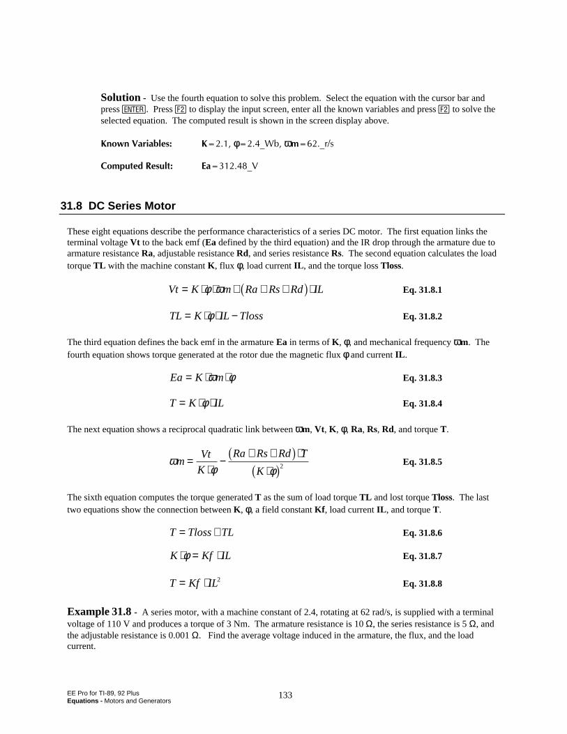
EE Pro for TI-89, 92 PlusEquations - Motors and Generators
133
Solution - Use the fourth equation to solve this problem. Select the equation with the cursor bar andpress . Press „ to display the input screen, enter all the known variables and press „ to solve theselected equation. The computed result is shown in the screen display above.
-PQYP8CTKCDNGU -φA9DωOATU
%QORWVGF4GUWNV 'CA8
31.8 DC Series Motor
These eight equations describe the performance characteristics of a series DC motor. The first equation links theterminal voltage Vt to the back emf (Ea defined by the third equation) and the IR drop through the armature due toarmature resistance Ra, adjustable resistance Rd, and series resistance Rs. The second equation calculates the loadtorque TL with the machine constant K , flux φ, load current IL , and the torque loss Tloss.
Vt K m Ra Rs Rd IL= ⋅ ⋅ + + + ⋅φ ω b g Eq. 31.8.1
TL K IL Tloss= ⋅ ⋅ −φ Eq. 31.8.2
The third equation defines the back emf in the armature Ea in terms of K , φ, and mechanical frequency ωm. Thefourth equation shows torque generated at the rotor due the magnetic flux φ and current IL .
Ea K m= ⋅ ⋅ω φ Eq. 31.8.3
T K IL= ⋅ ⋅φ Eq. 31.8.4
The next equation shows a reciprocal quadratic link between ωm, Vt , K , φ, Ra, Rs, Rd, and torque T.
ωφ φ
mVt
K
Ra Rs Rd T
K=
⋅−
+ + ⋅⋅
b gb g2 Eq. 31.8.5
The sixth equation computes the torque generated T as the sum of load torque TL and lost torque Tloss. The lasttwo equations show the connection between K , φ, a field constant Kf , load current IL , and torque T.
T Tloss TL= + Eq. 31.8.6
K Kf IL⋅ = ⋅φ Eq. 31.8.7
T Kf IL= ⋅ 2 Eq. 31.8.8
Example 31.8 - A series motor, with a machine constant of 2.4, rotating at 62 rad/s, is supplied with a terminalvoltage of 110 V and produces a torque of 3 Nm. The armature resistance is 10 Ω, the series resistance is 5 Ω, andthe adjustable resistance is 0.001 Ω. Find the average voltage induced in the armature, the flux, and the loadcurrent.
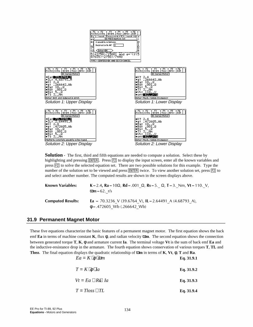
EE Pro for TI-89, 92 PlusEquations - Motors and Generators
134
Solution 1: Upper Display Solution 1: Lower Display
Solution 2: Upper Display Solution 2: Lower Display
Solution - The first, third and fifth equations are needed to compute a solution. Select these byhighlighting and pressing . Press „ to display the input screen, enter all the known variables andpress „ to solve the selected equation set. There are two possible solutions for this example. Type thenumber of the solution set to be viewed and press twice. To view another solution set, press „ toand select another number. The computed results are shown in the screen displays above.
-PQYP8CTKCDNGU -4CΩ4FAΩ4UAΩ6A0O8VA8
ωωOATU
%QORWVGF4GUWNVU 'CA8A8+.A#A#
φφA9DA9D
31.9 Permanent Magnet Motor
These five equations characterize the basic features of a permanent magnet motor. The first equation shows the backemf Ea in terms of machine constant K , flux φφ, and radian velocity ωωm. The second equation shows the connectionbetween generated torque T, K , φφ and armature current Ia. The terminal voltage Vt is the sum of back emf Ea andthe inductive-resistance drop in the armature. The fourth equation shows conservation of various torques T, TL andTloss. The final equation displays the quadratic relationship of ωωm in terms of K , Vt , φφ, T and Ra.
Ea K m= ⋅ ⋅φ ω Eq. 31.9.1
T K Ia= ⋅ ⋅φ Eq. 31.9.2
Vt Ea Ra Ia= + ⋅ Eq. 31.9.3
T Tloss TL= + Eq. 31.9.4
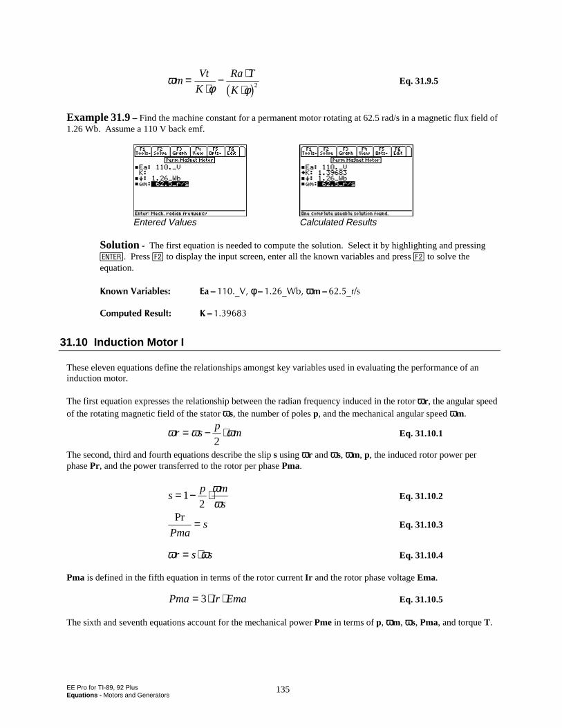
EE Pro for TI-89, 92 PlusEquations - Motors and Generators
135
ωφ φ
mVt
K
Ra T
K=
⋅− ⋅
⋅b g2 Eq. 31.9.5
Example 31.9 – Find the machine constant for a permanent motor rotating at 62.5 rad/s in a magnetic flux field of1.26 Wb. Assume a 110 V back emf.
Entered Values Calculated Results
Solution - The first equation is needed to compute the solution. Select it by highlighting and pressing¸. Press „ to display the input screen, enter all the known variables and press „ to solve theequation.
-PQYP8CTKCDNGU 'CA8φφA9DωωOATU
%QORWVGF4GUWNV -
31.10 Induction Motor I
These eleven equations define the relationships amongst key variables used in evaluating the performance of aninduction motor.
The first equation expresses the relationship between the radian frequency induced in the rotor ωωr , the angular speedof the rotating magnetic field of the stator ωωs, the number of poles p, and the mechanical angular speed ωωm.
ω ω ωr sp
m= − ⋅2
Eq. 31.10.1
The second, third and fourth equations describe the slip s using ωωr and ωωs, ωωm, p, the induced rotor power perphase Pr, and the power transferred to the rotor per phase Pma.
sp m
s= − ⋅1
2
ωω
Eq. 31.10.2
Pr
Pmas= Eq. 31.10.3
ω ωr s s= ⋅ Eq. 31.10.4
Pma is defined in the fifth equation in terms of the rotor current Ir and the rotor phase voltage Ema.
Pma Ir Ema= ⋅ ⋅3 Eq. 31.10.5
The sixth and seventh equations account for the mechanical power Pme in terms of p, ωωm, ωωs, Pma, and torque T.
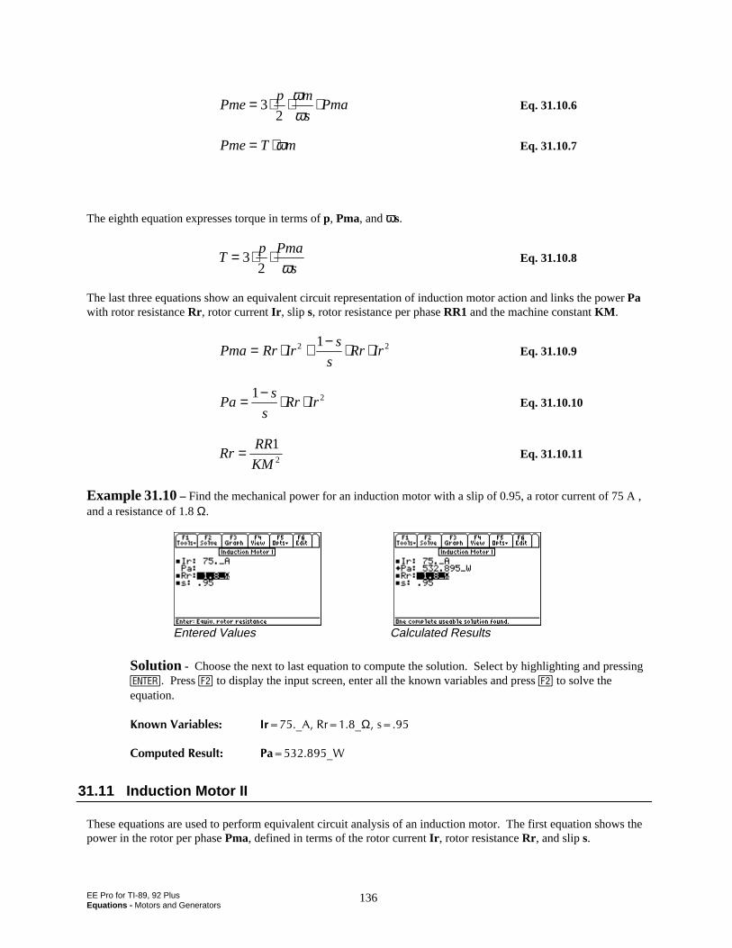
EE Pro for TI-89, 92 PlusEquations - Motors and Generators
136
Pmep m
sPma= ⋅ ⋅ ⋅3
2
ωω
Eq. 31.10.6
Pme T m= ⋅ω Eq. 31.10.7
The eighth equation expresses torque in terms of p, Pma, and ωωs.
Tp Pma
s= ⋅ ⋅3
2 ωEq. 31.10.8
The last three equations show an equivalent circuit representation of induction motor action and links the power Pawith rotor resistance Rr , rotor current Ir , slip s, rotor resistance per phase RR1 and the machine constant KM .
Pma Rr Irs
sRr Ir= ⋅ + − ⋅ ⋅2 21
Eq. 31.10.9
Pas
sRr Ir= − ⋅ ⋅1 2 Eq. 31.10.10
RrRR
KM= 1
2Eq. 31.10.11
Example 31.10 – Find the mechanical power for an induction motor with a slip of 0.95, a rotor current of 75 A ,and a resistance of 1.8 Ω.
Entered Values Calculated Results
Solution - Choose the next to last equation to compute the solution. Select by highlighting and pressing¸. Press „ to display the input screen, enter all the known variables and press „ to solve theequation.
-PQYP8CTKCDNGU +TA#4TAΩU
%QORWVGF4GUWNV 2CA9
31.11 Induction Motor II
These equations are used to perform equivalent circuit analysis of an induction motor. The first equation shows thepower in the rotor per phase Pma, defined in terms of the rotor current Ir , rotor resistance Rr , and slip s.
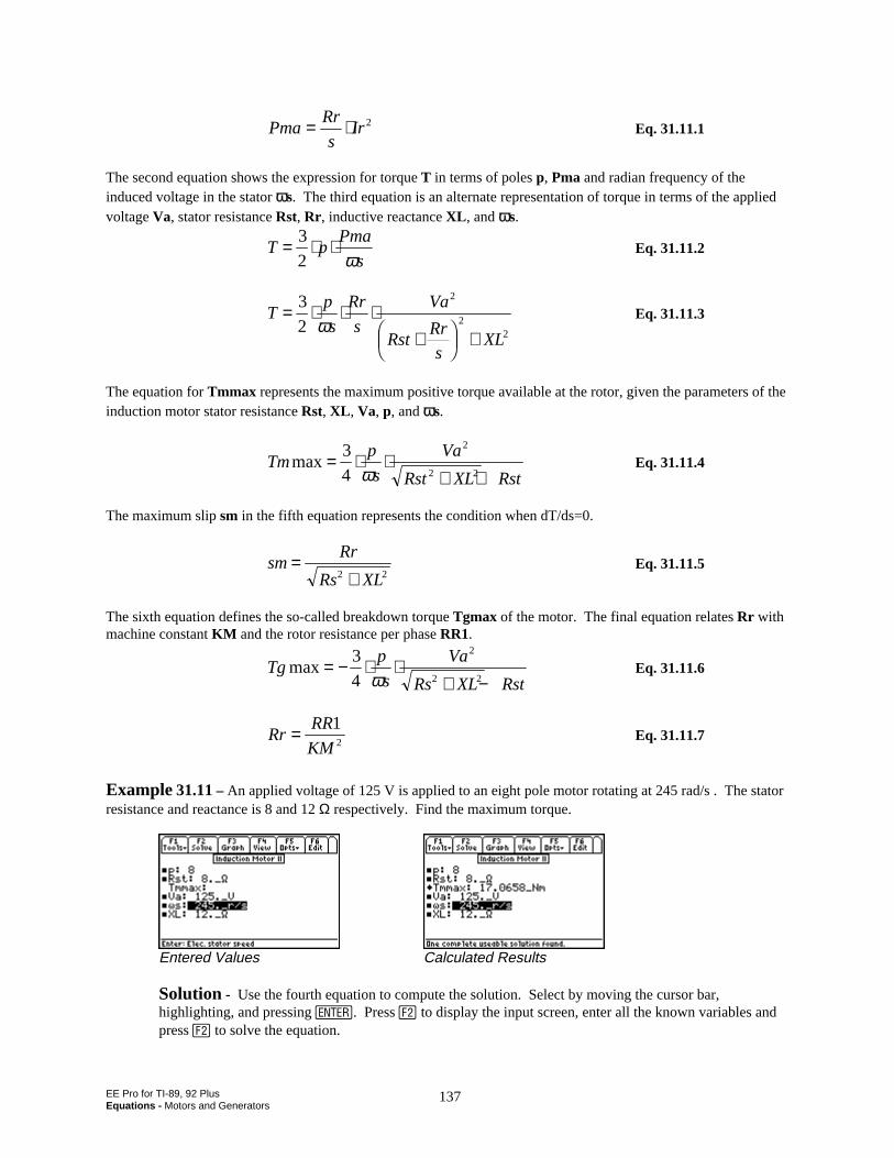
EE Pro for TI-89, 92 PlusEquations - Motors and Generators
137
PmaRr
sIr= ⋅ 2 Eq. 31.11.1
The second equation shows the expression for torque T in terms of poles p, Pma and radian frequency of theinduced voltage in the stator ωωs. The third equation is an alternate representation of torque in terms of the appliedvoltage Va, stator resistance Rst, Rr , inductive reactance XL , and ωωs.
T pPma
s= ⋅ ⋅3
2 ωEq. 31.11.2
Tp
s
Rr
s
Va
RstRr
sXL
= ⋅ ⋅ ⋅+F
HGIKJ +
3
2
2
22ω
Eq. 31.11.3
The equation for Tmmax represents the maximum positive torque available at the rotor, given the parameters of theinduction motor stator resistance Rst, XL , Va, p, and ωωs.
Tmp
s
Va
Rst XL Rstmax= ⋅ ⋅
+ +3
4
2
2 2ωEq. 31.11.4
The maximum slip sm in the fifth equation represents the condition when dT/ds=0.
smRr
Rs XL=
+2 2Eq. 31.11.5
The sixth equation defines the so-called breakdown torque Tgmax of the motor. The final equation relates Rr withmachine constant KM and the rotor resistance per phase RR1.
Tgp
s
Va
Rs XL Rstmax= − ⋅ ⋅
+ −3
4
2
2 2ωEq. 31.11.6
RrRR
KM= 1
2Eq. 31.11.7
Example 31.11 – An applied voltage of 125 V is applied to an eight pole motor rotating at 245 rad/s . The statorresistance and reactance is 8 and 12 Ω respectively. Find the maximum torque.
Entered Values Calculated Results
Solution - Use the fourth equation to compute the solution. Select by moving the cursor bar,highlighting, and pressing . Press „ to display the input screen, enter all the known variables andpress „ to solve the equation.
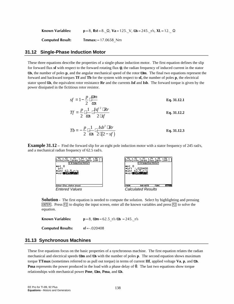
EE Pro for TI-89, 92 PlusEquations - Motors and Generators
138
-PQYP8CTKCDNGU R4UVAΩ8CA8ωωUATU:.AΩ
%QORWVGF4GUWNV 6OOCZA0O
31.12 Single-Phase Induction Motor
These three equations describe the properties of a single-phase induction motor. The first equation defines the slipfor forward flux sf with respect to the forward rotating flux φ, the radian frequency of induced current in the statorωs, the number of poles p, and the angular mechanical speed of the rotor ωm. The final two equations represent theforward and backward torques Tf and Tb for the system with respect to sf, the number of poles p, the electricalstator speed ωs, the equivalent rotor resistance Rr and the currents Isf and Isb. The forward torque is given by thepower dissipated in the fictitious rotor resistor.
sfp m
s= − ⋅1
2
ωω
Eq. 31.12.1
Tfp
s
Isf Rr
sf= ⋅ ⋅ ⋅
⋅2
1
2
2
ωEq. 31.12.2
Tbp
s
Isb Rr
sf= − ⋅ ⋅ ⋅
⋅ −2
1
2 2
2
ω b g Eq. 31.12.3
Example 31.12 – Find the forward slip for an eight pole induction motor with a stator frequency of 245 rad/s,and a mechanical radian frequency of 62.5 rad/s.
Entered Values Calculated Results
Solution - The first equation is needed to compute the solution. Select by highlighting and pressing¸. Press „ to display the input screen, enter all the known variables and press „ to solve theequation.
-PQYP8CTKCDNGU RωOATUωU ATU
%QORWVGF4GUWNVU UH
31.13 Synchronous Machines
These five equations focus on the basic properties of a synchronous machine. The first equation relates the radianmechanical and electrical speeds ωm and ωs with the number of poles p. The second equation shows maximumtorque TTmax (sometimes referred to as pull out torque) in terms of current IIf , applied voltage Va, p, and ωs.Pma represents the power produced in the load with a phase delay of θ. The last two equations show torquerelationships with mechanical power Pme, ωm, Pma, and ωs.
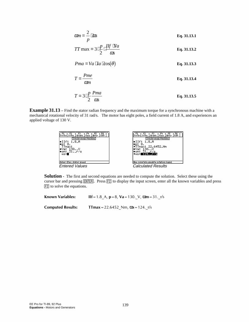
EE Pro for TI-89, 92 PlusEquations - Motors and Generators
139
ω ωmp
s= ⋅2Eq. 31.13.1
TTp IIf Va
smax= ⋅ ⋅ ⋅
32 ω
Eq. 31.13.2
Pma Va Ia= ⋅ ⋅cosθb g Eq. 31.13.3
TPme
m=
ωEq. 31.13.4
Tp Pma
s= ⋅3
2 ωEq. 31.13.5
Example 31.13 – Find the stator radian frequency and the maximum torque for a synchronous machine with amechanical rotational velocity of 31 rad/s. The motor has eight poles, a field current of 1.8 A, and experiences anapplied voltage of 130 V.
Entered Values Calculated Results
Solution - The first and second equations are needed to compute the solution. Select these using thecursor bar and pressing . Press „ to display the input screen, enter all the known variables and press„ to solve the equations.
-PQYP8CTKCDNGU ++HA#R8CA8ωωOATU
%QORWVGF4GUWNVU 66OCZA0OωωUATU
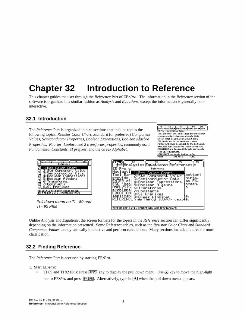
EE Pro for TI - 89, 92 PlusReference - Introduction to Reference Section
1
Chapter 32 Introduction to ReferenceThis chapter guides the user through the Reference Part of EE•Pro. The information in the Reference section of thesoftware is organized in a similar fashion as Analysis and Equations, except the information is generally non-interactive.
32.1 Introduction
The Reference Part is organized in nine sections that include topics thefollowing topics: Resistor Color Chart, Standard (or preferred) ComponentValues, Semiconductor Properties, Boolean Expressions, Boolean AlgebraProperties, Fourier, Laplace and z transforms properties, commonly usedFundamental Constants, SI prefixes, and the Greek Alphabet.
Pull down menu on TI - 89 andTI - 92 Plus
Unlike Analysis and Equations, the screen formats for the topics in the Reference section can differ significantly,depending on the information presented. Some Reference tables, such as the Resistor Color Chart and StandardComponent Values, are dynamically interactive and perform calculations. Many sections include pictures for moreclarification.
32.2 Finding Reference
The Reference Part is accessed by starting EE•Pro.
1. Start EE•Pro:• TI 89 and TI 92 Plus: Press O key to display the pull down menu. Use D key to move the high-light
bar to EE•Pro and press . Alternatively, type in [A] when the pull down menu appears.
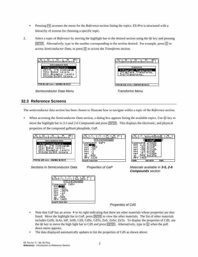
EE Pro for TI - 89, 92 PlusReference - Introduction to Reference Section
2
• Pressing † accesses the menu for the Reference section listing the topics. EE•Pro is structured with a
hierarchy of screens for choosing a specific topic. 2. Select a topic of Reference by moving the highlight bar to the desired section using the D key and pressing
¸. Alternatively, type in the number corresponding to the section desired. For example, press ª to
access Semiconductor Data, or press to access the Transforms section.
Semiconductor Data Menu Transforms Menu
32.3 Reference Screens
The semiconductor data section has been chosen to illustrate how to navigate within a topic of the Reference section.
• When accessing the Semiconductor Data section, a dialog box appears listing the available topics. Use D key to
move the highlight bar to 3-5 and 2-6 Compounds and press . This displays the electronic, and physical
properties of the compound gallium phosphide, GaP.
Sections in Semiconductor Data Properties of GaP Materials available in 3-5, 2-6 Compounds section
Properties of CdS
• Note that GaP has an arrow ! to its right indicating that there are other materials whose properties are alsolisted. Move the highlight bar to GaP, press to view the other materials. The list of other materialsincludes GaSb, InAs, InP, InSb, CdS, CdSe, CdTe, ZnS, ZnSe, ZnTe. To display the properties of CdS, usethe D key to move the high light bar to CdS and press . Alternatively, type in when the pulldown menu appears.
• The data displayed automatically updates to list the properties of CdS as shown above.
EE Pro for TI - 89, 92 PlusReference - Introduction to Reference Section
3
• Other properties available in the section include Donor and Acceptor levels in Silicon shown in the screen
displays below.
Silicon Donor Level Silicon Acceptor Levels
The last topic in Semiconductor Properties includes the colors observed for Silicon dioxide and Silicon Nitridethickness. These colors are arranged in order of thickness (µm). Some colors appear multiple times due to multiplediffraction orders.
SiO2/Si3N4 Color Choices Properties of SiO2/Si3N4(thickness in µm)
32.4 Using Reference Tables
The Transform section is used as an example of viewing reference tables. Transforms allows the user to inspectFourier, Laplace or z-transforms. Each of these topics are divided into three sub-topics, Definitions, Properties andTransform Pairs. For example, navigate from Transforms → Fourier Transforms → Transform Properties. Ascreen display below shows the lists the equations displaying the fundamental properties of Fourier transform pairs.Note that the name of the selected transform equation appears in the status line. For example, if the highlight bar ismoved to the sixth equation, the status line displays "Rectangular Pulse" as the description of the property.
Normal View Inverse View (press †)
To view the equation in Pretty Print format, press B. The contents on the right side of the colon (:) are displayed in
Pretty Print, while the contents to the left of the colon are displayed in regular type above the status line. To reversethis display (display the inverse of the property), press N to exit Pretty Print mode, press † to display the inverse
form of the transform property, and B to view the inverse transform in PrettyPrint.

EE Pro for TI - 89, 92 PlusReference - Introduction to Reference Section
4
Regular View of Laplace Transform Inverse View of Laplace Transform

EE Pro for TI - 89, 92 PlusReference - Resistor Color Chart
5
Chapter 33 Resistor Color Chart
This section of EE•Pro allows the user to enter the color sequence of aphysical resistor and compute its value and tolerance. Most physicalresistors come with a band of colors to help identify its value. There are 3variations of color bands used in practice: 3, 4 or 5 band of colors. Thetable below identifies the hierarchy used in practice. A picture of thecolor chart is included in the software and is displayed when the functionkey † is pressed.
Table 33-1 Description of Colors in resistors
Band positions represent:3-Band 4-Band 5-Band
Band 1 digit digit digitBand 2 digit digit digitBand 3 multiplier multiplier digitBand 4 N/A tolerance multiplier
Band positions represent:3-Band 4-Band 5-Band
Band 1 digit digit digitBand 2 digit digit digitBand 3 multiplier multiplier digitBand 4 N/A tolerance multiplierBand 5 N/A N/A tolerance
Colors represent:DIGIT MULTIPLIER TOLERANCE
SILVER - ÷E2 10%GOLD - ÷E1 5%BLACK 0 xE0 -BROWN 1 xE1 1%RED 2 xE2 2%ORANGE 3 xE3 -YELLOW 4 xE4 -GREEN 5 xE5 0.5%
EE Pro for TI - 89, 92 PlusReference - Resistor Color Chart
6
BLUE 6 xE6 0.25%VIOLET 7 xE7 0.1%GREY 8 xE8 0.05%WHITE 9 xE9 -
Field DescriptionInput FieldsNum. of Bands : (Number of Bands) Pressing displays choice of 3, 4, or 5 bands.Band 1 : (see table above) Pressing displays choice of colors.Band 2 : (see table above) Pressing displays choice of colors.Band 3 : (see table above) Pressing displays choice of colors.Band 4 : (see table above) Pressing displays choice of colors.Band 5 : (see table above) Pressing displays choice of colors.
Output FieldsValue : (Resistor Value) Returns a Resistor Value.Tolerance : (Resistor Tolerance) Returns a percent.
33.1 Using the Resistor Color Chart
Select this topic from the Reference section and press .
1. Select the number of bands on the resistor (display automatically updates for the entry).2. In each Band field , select a color using B and pressing .
3. The results are displayed in the Value and Tolerance lines of the display.
Example 33.1- Find the value and tolerance of a resistor with band colors yellow, black, red and gold.Using the steps outlined above.
1. Enter 4 for Num. of Bands .2. For the 1st Digit Band , select Yellow color.3. For the 2nd Digit Band , select Black color.4. For the Multiplier Band , select Red color.5. For Tolerance Band , select Gold.6. The results show 4000_Ω in the Value field, and ±
5% in the Tolerance field as shown to the right.
EE Pro for TI - 89, 92 PlusReference - Standard Component Values
7
Chapter 34 Standard Component ValuesIn this section, the software computes the inverse of the color chart computation described in the previous chapter(i.e.: given a value and a tolerance for a resistor, a color sequence is generated). As a side benefit the calculationalgorithm also allows the user to estimate suitable “off-the-shelf” standard components for needed resistors,inductors and capacitors. These are also referred to as "Preferred Values" of components available frommanufacturers.
Field DescriptionsInput FieldValue : (Desired Value or Design Spec.) Enter a real number.Tolerance : (Tolerance of Component) Press to display selection.
The values range from tolerance ±20% down to±.0.05%.
Component : (Type of Component) Press to display component choices: Resistor,Inductor, or Capacitor.
Output FieldValue : (Closest Standard Value to the Desired Value) Returns a "Preferred Value".Bands : (Resistor Color Bands - if the Component is a Resistor ) Returns the color bands in a resistor.
Example 34.1 - A design calculation yields 2.6 microfarads for a capacitor. Find the closest preferred value witha tolerance of 1%.
Use the following directions:
1. Press the 3 setting and set Display Digits to FLOAT 8, press ¸.
2. In the Value field, enter 2.6E-6.3. In the Tolerance field, press to display choices; use D key
to move the highlight bar ±1 % and press .4. In the Component field, press to display; use D key to
move the highlight bar to "Capacitor" and press to select.5. The Standard Component Value is displayed as 2.61E-6_F.
EE Pro for TI-89, 92 PlusReference - Semiconductor data
8
Chapter 35 Semiconductor DataPhysical, chemical, electrical, electronic and mechanical properties of common semiconductors are presented in thissection. The information is organized under five (5) topics listed in detail in Table 35-1. All properties are listed at300 °K, unless otherwise specifically stated. Details of how to access the information is included in the table.
Table 35-1 Semiconductor DataSection Label Data Fields DescriptionSemiconductors Input Field:
Semiconductor:
Atoms: (Atoms)At Wt: (Atomic Weight) Br Fld: (Breakdown Field)xtal: (Crystal Structure)ρ: (Density) εr: (Relative permittivity) Nc: (Density of states, CB)Nv: (Density of states, VB)mle: (Longitudinal e- mass)mte: (Transverse e-mass) mlh: (Light hole mass)mhh: (Heavy hole mass) φ: (Electron affinity)EG:(Band gap)ni: (Intrinsic Density)a: (Lattice constant)αth: (Thermal expansion coefficient)MP:(Melting Point) τ: (Carrier lifetime)µn: (Electron mobility)µp: (Hole Mobility)Raman E: (Raman Photon Energy)Sp Ht: (Specific heat)Th. Cond: (Thermal conductivity)Diff Cons: (Diffusion Constant)Vapor Pr: (Vapor Pressure 1600°C)Vapor Pr: (Vapor Pressure 930°C)Work Fn: (Work Function)
Press ¸ to display options (Sior GaAs), use D to move thehighlighter to Si or GaAs and press¸ to select1/cm3
g/molV/cmstructure nameg/cm 3
unitless1/cm3
1/cm3
unitless###VeV1/cm3
nm1/°K°Cscm2/(V*s)cm2/(V*s)eVJ/gW/(cm*°K)cm2/storrtorrV
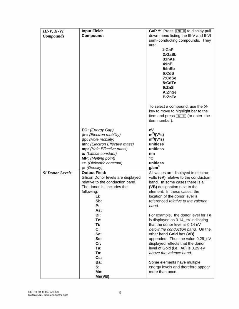
EE Pro for TI-89, 92 PlusReference - Semiconductor data
9
III-V, II-VICompounds
Input Field:Compound:
EG: (Energy Gap)µn: (Electron mobility)µp: (Hole mobility)mn: (Electron Effective mass)mp: (Hole Effective mass)a: (Lattice constant)MP: (Melting point)εr: (Dielectric constant)ρ: (Density)
GaP ! Press ¸ to display pulldown menu listing the III-V and II-VIsemi-conducting compounds. Theyare: 1:GaP
2:GaSb3:InAs4:InP5:InSb6:CdS7:CdSe8:CdTeœ
9:ZnSA:ZnSeB:ZnTe
To select a compound, use the Dkey to move to highlight bar to theitem and press ¸ (or enter theitem number).
eVm2/(V*s)m2/(V*s)unitlessunitlessnm°Cunitlessg/cm 3
Si Donor Levels Output Field:Silicon Donor levels are displayedrelative to the conduction band.The donor list includes thefollowing:
Li:Sb:P:As:Bi:Te:Ti:C:Se:Se:Cr:Ta:Ta:Cs:Ba:S:Mn:Mn(VB):
All values are displayed in electronvolts (eV) relative to the conductionband. In some cases there is a(VB) designation next to theelement. In these cases, thelocation of the donor level isreferenced relative to the valenceband.
For example, the donor level for Teis displayed as 0.14_eV indicatingthat the donor level is 0.14 eVbelow the conduction band. On theother hand Gold has (VB)appended. Thus the value 0.29_eVdisplayed reflects that the donorlevel of Gold (i.e., Au) is 0.29 eVabove the valence band.
Some elements have multipleenergy levels and therefore appearmore than once.

EE Pro for TI-89, 92 PlusReference - Semiconductor data
10
Ag(VB):Pt(VB):Si(VB):Si(VB):Na(VB):Au(VB):V:Mo:Mo(VB):Mo(VB):Hg(VB):Hg(VB):Sr:Sr(VB):Ge:Ge(VB):K:K(VB):Sn:W:W:W:W(VB):W(VB):Pb:O:O:Fe:Fe:Fe(VB):
Acceptor Levels Output Field:Silicon Acceptor levels aredisplayed relative to the valenceband. The acceptor list includesthe following:
Mg(CB):Mg(CB):Cs:Ba:S:Mn:Ag(CB):Cd(CB):Cd(CB):Cd:Pt(CB):Pt:Si:B:Al:Ga:In:Tl:
All values in are in electron volts(eV) relative to the valence band.For some elements, there is a (CB)appended to the element name. Inthese cases, the location of theacceptor level is referenced relativeto the conduction band.
For example, the acceptor level forMg is displayed as 0.11_eV. (CB)follows the element name Mgindicating that the acceptor level is0.11_eV below the conductionband.
On the other hand, Platinum (Pt)has a value of 0.36 eV, with noadditional information. This is anindicator that Pt produces anacceptor level 0.36 eV above thevalence band.
Some elements have multiple levels

EE Pro for TI-89, 92 PlusReference - Semiconductor data
11
Pd:Be:Be:Zn(CB):Zn:Au(CB):Co(CB):Co:Co:V:Ni(CB):Hg(CB):Hg(CB):Cu:Cu:Cu:Sn:Pb:O(CB):O:
and appear more than once.
SiO2/Si3N4 Colors Input Field:Compound:
Once the specific color choice hasbeen made, the display fields showthe information for the followingparameters:
SiO2: Value in µmSi3N4: Value in µmOrder: Value as a number
Silicon ! Press ¸ to displaythe pull down menu listing the colorof silicon with SiO2 or Si3N4deposited on the surface.
1:Silicon2:Brown3:Golden brown4:Red5:Deep Blue6:Blue7:Pale Blue8:Very Pale Blue œ
9:SiliconA: Light Yellow ZnSeB: YellowC: Orange-RedD: RedE: Dark redF: BlueG: Blue GreenH: Light GreenI: Orange YellowJ: Red
To select a specific compound,enter the item number (or use Dkey) and press ¸
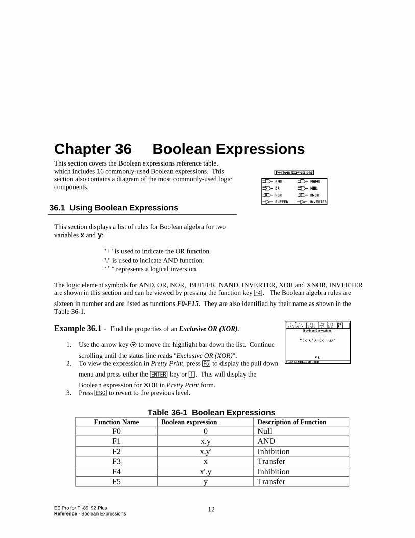
EE Pro for TI-89, 92 PlusReference - Boolean Expressions
12
Chapter 36 Boolean ExpressionsThis section covers the Boolean expressions reference table,which includes 16 commonly-used Boolean expressions. Thissection also contains a diagram of the most commonly-used logiccomponents.
36.1 Using Boolean Expressions
This section displays a list of rules for Boolean algebra for twovariables x and y:
"+" is used to indicate the OR function."." is used to indicate AND function." ' " represents a logical inversion.
The logic element symbols for AND, OR, NOR, BUFFER, NAND, INVERTER, XOR and XNOR, INVERTERare shown in this section and can be viewed by pressing the function key †. The Boolean algebra rules are
sixteen in number and are listed as functions F0-F15. They are also identified by their name as shown in theTable 36-1.
Example 36.1 - Find the properties of an Exclusive OR (XOR).
1. Use the arrow key D to move the highlight bar down the list. Continue
scrolling until the status line reads "Exclusive OR (XOR)".2. To view the expression in Pretty Print, press ‡ to display the pull down
menu and press either the key or . This will display the
Boolean expression for XOR in Pretty Print form.3. Press N to revert to the previous level.
Table 36-1 Boolean ExpressionsFunction Name Boolean expression Description of Function
F0 0 NullF1 x.y ANDF2 x.y' InhibitionF3 x TransferF4 x'.y InhibitionF5 y Transfer
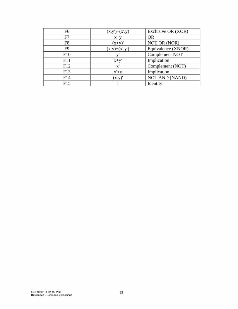
EE Pro for TI-89, 92 PlusReference - Boolean Expressions
13
F6 (x.y')+(x'.y) Exclusive OR (XOR)F7 x+y ORF8 (x+y)' NOT OR (NOR)F9 (x.y)+(x'.y') Equivalence (XNOR)F10 y' Complement NOTF11 x+y' ImplicationF12 x' Complement (NOT)F13 x'+y ImplicationF14 (x.y)' NOT AND (NAND)F15 1 Identity
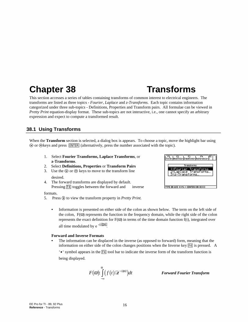
EE Pro for TI - 89, 92 PlusReference - Transforms
16
Chapter 38 TransformsThis section accesses a series of tables containing transforms of common interest to electrical engineers. Thetransforms are listed as three topics - Fourier, Laplace and z-Transforms. Each topic contains informationcategorized under three sub-topics - Definitions, Properties and Transform pairs. All formulae can be viewed inPretty Print equation-display format. These sub-topics are not interactive, i.e., one cannot specify an arbitraryexpression and expect to compute a transformed result.
38.1 Using Transforms
When the Transform section is selected, a dialog box is appears. To choose a topic, move the highlight bar usingD or Ckeys and press (alternatively, press the number associated with the topic).
1. Select Fourier Transforms, Laplace Transforms, or z-Transforms.2. Select Definitions, Properties or Transform Pairs3. Use the D or C keys to move to the transform line
desired.4. The forward transforms are displayed by default.
Pressing † toggles between the forward and inverse
formats.5. Press B to view the transform property in Pretty Print.
• Information is presented on either side of the colon as shown below. The term on the left side ofthe colon, F(ω) represents the function in the frequency domain, while the right side of the colonrepresents the exact definition for F(ω) in terms of the time domain function f(t), integrated over
all time modulated by e -i⋅ω⋅t. Forward and Inverse Formats• The information can be displaced in the inverse (as opposed to forward) form, meaning that the
information on either side of the colon changes positions when the Inverse key † is pressed. A
‘é‘ symbol appears in the † tool bar to indicate the inverse form of the transform function is
being displayed.
F f t e dti tω ωb g b gc h: ⋅ − ⋅ ⋅
−∞
+∞
z Forward Fourier Transform
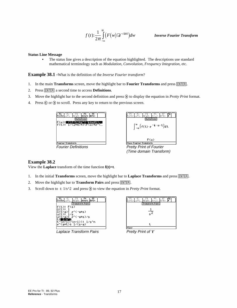
EE Pro for TI - 89, 92 PlusReference - Transforms
17
f t F w e dwi t( ):1
2πωb gc h⋅ − ⋅ ⋅
−∞
+∞
z Inverse Fourier Transform
Status Line Message
• The status line gives a description of the equation highlighted. The descriptions use standardmathematical terminology such as Modulation, Convolution, Frequency Integration, etc.
Example 38.1 -What is the definition of the Inverse Fourier transform?
1. In the main Transforms screen, move the highlight bar to Fourier Transforms and press .
2. Press a second time to access Definitions.
3. Move the highlight bar to the second definition and press B to display the equation in Pretty Print format.
4. Press A or B to scroll. Press any key to return to the previous screen.
Fourier Definitions Pretty Print of Fourier(Time domain Transform)
Example 38.2View the Laplace transform of the time function f(t)=t .
1. In the initial Transforms screen, move the highlight bar to Laplace Transforms and press .
2. Move the highlight bar to Transform Pairs and press .
3. Scroll down to t: 1/s^2 and press B to view the equation in Pretty Print format.
Laplace Transform Pairs Pretty Print of ‘t’
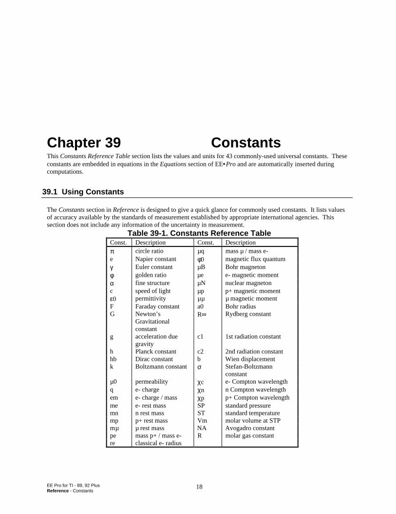
EE Pro for TI - 89, 92 PlusReference - Constants
18
Chapter 39 ConstantsThis Constants Reference Table section lists the values and units for 43 commonly-used universal constants. Theseconstants are embedded in equations in the Equations section of EE•Pro and are automatically inserted duringcomputations.
39.1 Using Constants
The Constants section in Reference is designed to give a quick glance for commonly used constants. It lists valuesof accuracy available by the standards of measurement established by appropriate international agencies. Thissection does not include any information of the uncertainty in measurement.
Table 39-1. Constants Reference TableConst. Description Const. Descriptionπ circle ratio µq mass µ / mass e-e Napier constant φ0 magnetic flux quantumγ Euler constant µB Bohr magnetonφ golden ratio µe e- magnetic momentα fine structure µN nuclear magnetonc speed of light µp p+ magnetic momentε0 permittivity µµ µ magnetic momentF Faraday constant a0 Bohr radiusG Newton’s
Gravitationalconstant
R∞ Rydberg constant
g acceleration duegravity
c1 1st radiation constant
h Planck constant c2 2nd radiation constanthb Dirac constant b Wien displacementk Boltzmann constant σ Stefan-Boltzmann
constantµ0 permeability χc e- Compton wavelengthq e- charge χn n Compton wavelengthem e- charge / mass χp p+ Compton wavelengthme e- rest mass SP standard pressuremn n rest mass ST standard temperaturemp p+ rest mass Vm molar volume at STPmµ µ rest mass NA Avogadro constantpe mass p+ / mass e- R molar gas constantre classical e- radius

EE Pro for TI - 89, 92 PlusReference - Constants
19
These constants were arranged in the following order: universal mathematical constants lead the list followed byuniversal physical constants, atomic and quantum mechanical constants, radiation constants, standard temperatureand pressure, universal gas constant and molar constants. To view a constant, use the arrow key D key to move the
highlight bar to the value and press the View key †. The status line at the bottom of the screen gives a verbal
description of the constant.
Example 39.1- Look up the value of π.
1. Pi is the first value to appear in the constant sections. Make sure it is selected by the highlight bar using thearrow keys.
2. Access the View function by pressing key †.
3. Press any key to return to the constants screen.
The number of significant digits displayed in Pretty Print can be changed in the 3 setting.
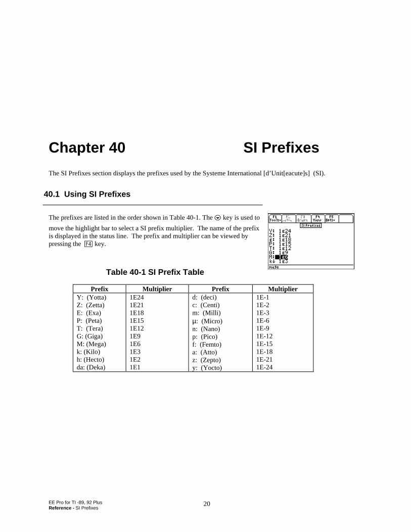
EE Pro for TI -89, 92 PlusReference - SI Prefixes
20
Chapter 40 SI Prefixes
The SI Prefixes section displays the prefixes used by the Systeme International [d’Unit[eacute]s] (SI).
40.1 Using SI Prefixes
The prefixes are listed in the order shown in Table 40-1. The D key is used to
move the highlight bar to select a SI prefix multiplier. The name of the prefixis displayed in the status line. The prefix and multiplier can be viewed bypressing the † key.
Table 40-1 SI Prefix Table
Prefix Multiplier Prefix MultiplierY: (Yotta)Z: (Zetta)E: (Exa)P: (Peta)T: (Tera)G: (Giga)M: (Mega)k: (Kilo)h: (Hecto)da: (Deka)
1E241E211E181E151E121E91E61E31E21E1
d: (deci)c: (Centi)m: (Milli)µ: (Micro)n: (Nano)p: (Pico)f: (Femto)a: (Atto)z: (Zepto)y: (Yocto)
1E-11E-21E-31E-61E-91E-121E-151E-181E-211E-24
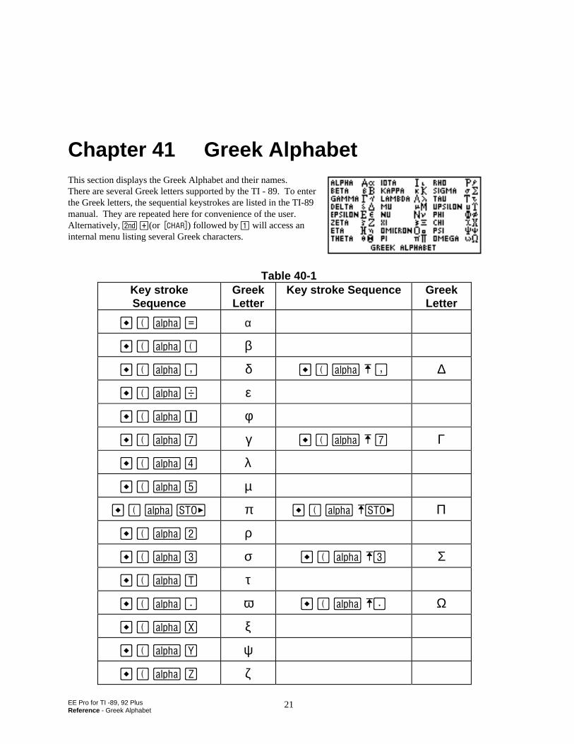
EE Pro for TI -89, 92 PlusReference - Greek Alphabet
21
Chapter 41 Greek AlphabetThis section displays the Greek Alphabet and their names.There are several Greek letters supported by the TI - 89. To enterthe Greek letters, the sequential keystrokes are listed in the TI-89manual. They are repeated here for convenience of the user.Alternatively, 2 «(or ¿) followed by will access aninternal menu listing several Greek characters.
Table 40-1Key strokeSequence
GreekLetter
Key stroke Sequence GreekLetter
¥ c j Á α
¥ c j c β
¥ c j b δ ¥ c j Î b ∆
¥ c j e ε
¥ c j Í φ
¥ c j m γ ¥ c j Î m Γ
¥ c j y λ
¥ c j z µ
¥ c j § π ¥ c j Χ Π
¥ c j © ρ
¥ c j ª σ ¥ c j Ϊ Σ
¥ c j Ü τ
¥ c j ¶ ω ¥ c j ζ Ω
¥ c j Ù ξ
¥ c j Ú ψ
¥ c j Û ζ

EE Pro for TI-89, 92 PlusAppendix A - Frequently Asked Questions
1
Appendix A Frequently Asked QuestionsA complete list of commonly asked questions about the EE•Pro are listed here. Review this list for your questionsprior to calling for Technical support. You might save yourself a phone call! The material is covered under fourgeneral headings.
A.1 Questions and Answers
General QuestionsAnalysis Questions
Equations QuestionsReference Questions
A.2 General Questions
The following is a list of questions about the general features of EE•Pro: Q. Where can I find additional information about a variable?A. A brief description of a highlighted variable appears in the status line at the bottom of the screen. Moreinformation, including its allowable entry parameters (i.e.: whether complex, symbolic or negative values can beentered, etc.) can be accessed by pressing ‡/Opts and 2:Type .
Q. What does the underscore “_” next to a variable mean?A. This designates a variable which allows entry or expression of complex values.
Q . I am in the middle of a computation and nothing seems to be occurring. How can I halt this process? A. Some computations can take a long time, particular if many equations and unknowns are being solved or acomplex analysis function has been entered. Notice if the message in the status line at the bottom-right of thescreen reads BUSY. This indicates that the TI math engine is attempting to solve the problem. Pressing the ´
key usually halts a computation and allows the user to regain control of the software. If, for some reason, thecalculator locks up and does not allow user intervention, a “cold start” will have to be performed. This can bedone by holding down the three keys; 2, A, and B, and pressing . WARNING: This will delete folders
containing any defined variables or stored programs. Use it as a last resort. A "cold start" will not delete EE•Profrom your calculator. Q What do three dots (...) mean at the end of an item on the screen? A. The three dots (an ellipsis) indicate the item is too wide to fit on the available screen area. To view an item inits entirety, select it by moving the highlight bar and press † (or B, in some cases) to view the item in Pretty
Print. Press A or B to scroll the item back and forth across the screen to view the entire object.
Q. How can I recall, or view values of a previously computed problem?
EE Pro for TI-89, 92 PlusAppendix A - Frequently Asked Questions
2
A. EE•Pro automatically stores its variables in the current folder specified by the user in 3 or the HOME
screens. The current folder name is displayed in the lower left corner of the screen (default is “Main”). To createa new folder to store values for a particular session of EE•Pro, press ƒ:/TOOLS, ª:/NEW and type the name of
the new folder (see Chapter 5 of the TI-89 Guidebook for the complete details of creating and managing folders). There are several ways to display or recall a value:
• The contents of variables in any folder can be displayed using the °, moving the cursor to the
variable name and pressing to display the contents of a particular variable.
• Variables in a current folder can be recalled in the HOME screen by typing the variable name.• Finally, values and units can be copied and recalled using the ƒ/Tools 5:COPY and 6:PASTE
feature.
All inputs and calculated results from Analysis and Equations section are saved as variable names. Previouslycalculated, or entered values for variables in a folder are replaced when equations are solved using new valuesfor inputs.
Q. Why is it that some of the values of variables saved earlier are cleared when I graph an equation or analysisfunction which uses the variable name(s)?
A. When an equation or analysis function is graphed, EE•Pro creates a function for the TI grapher which expressesthe dependent variable in terms of the independent variable. This function is stored under the variable namepro(x). When the EE•Pro’s equation grapher is executed, values are inserted into the independent variable forpro(x) and values for the dependent value are calculated. Whatever values which previously existed in either ofthe dependent and independent variables in the current folder are cleared. To preserve data under variable nameswhich may conflict with EE•Pro’s variables, run EE•Pro in a separate folder using the guidelines above.
Q. An item which is supposed to be displayed in a menu doesn’t appear.A. Some menus have more than eight items. If an arrow ï appears next to the digit 8, use the arrow key D to
scroll the menu and view the remaining topics or press 2 D jump to the bottom of the menu.
Q. Is there a help section in the software?A. There is a short series (slides) of general hints which can be accessed from the main screen of EE•Pro under‡/Info . A different message appears each time ‡ is pressed. We’ve attempted to keep most of the explanation
of certain topics to the manual in an effort to keep the software compact. Consult the chapter corresponding to theappropriate section of the software. If your are still in need of clarification, contact Texas Instruments (contactinformation in the Warranty and Technical Support section of the manual) A compiled list of the receivedquestions and answers will be posted periodically on the da Vinci website. http://www.dvtg.com/faq/eepro
A.3 Analysis Questions
These are some commonly asked questions about the Analysis section of EE•Pro.
Q. The screen display of computed results does not look identical to the example in the manual.A. The 3 setting, which controls the number of floating point digits displayed in a value and whether an
answer appears in exact or approximate form, may have been set differently on the calculator used to make thescreen displays for the example problem. Press the 3 key to view or change the mode settings. The first page
will display the number of floating point digits, whether the display is in NORMAL, SCIENTIFIC, ORENGINEERING exponential formats. Pressing „will display whether computed answers are displayed in
APPROXIMATE or EXACT formats. The default mode setting for EE•Pro is Float 6, Radian and Approximatecalculations.
EE Pro for TI-89, 92 PlusAppendix A - Frequently Asked Questions
3
Q. The calculated angle or radian frequency result isn’t correct.A. Check to be sure the 3 settings list degrees or radians for angle units and make sure it matches the units
of your entered value or desired value. Secondly, if the result is greater than 2π or less than -2π (result ≥ 360o),the TI solve(...) function may be generating a non principal solution. A principal solution is defined as a valuebetween 0 and 2π (or between 0 and 360o). A non principal solution can be converted to a principal solution byadding or subtracting integer multiples of 2π (or 360o) until the remainder is within the range of 0 and 2π (or 0 and360o). The remainder is the principal solution.
Example: Imagine solving the equation sin( ) .x = 0 5. Non principle solutions include: 30°, 390°, -330°, 750°, etc.,but the principal solution is 30°.
Q. The solution for an analysis function is expressed in symbolic terms or variables, whereas a numerical valuewas expected. Why?A. If a variable name is entered as an input, EE•Pro will calculate a solution in symbolic form. In cases where aparameter entry is left blank, the variable’s name will be used in a symbolic computation. A name cannot beentered which is identical to the variable name (i.e.: C for capacitance) instead, leave the entry blank.
Q. Units are not displayed in Analysis computations. Why?A. The Analysis section incorporates methods for calculation which are unique to each topic in analysis (asopposed to Equations which uses similar methods of calculation in all of the sections). Unit management wasomitted for simplicity. All entries and computed results in Analysis are assumed to be in common SI units (F, m,A, Ω, etc.) which are stated in the status line for each parameter. In some cases, variables will be expressed inunits arbitrarily chosen by the user (example: The variable len in Transmission Lines can be entered in km, m,miles however the answers will be expressed in units of len).
If a value is entered that is inconsistent with the expected data type, an error dialog will appear which lists theentry name, the description, and the expected data type(s). See Appendix E for details on error messages.
Q. What is the multiple graph feature in Capital Budgeting and how do I get it to plot several projectssimultaneously?A. Activating the multiple graph feature allows successive graphs to be overlayed on the same. To do this, thegraphing execution must be repeated each time a new project is plotted.1. Make sure the cash flows for all the named projects have been entered.2. Enable the Multiple Graphs feature by highlighting and pressing the key.
3. Select the name of a project you wish to graph and press ….
4. To overlay a second project on the first, select a different project name and press … to graph.
5. Repeat step 4 each time a new project is to be graphed on top of previously plotted functions.
A.4 Equations Questions
These are some common questions about the Equations section of EE•Pro. Q. There are already values stored in some of my variables. How do I clear or use those values? A. These values remain from previous solving operations. It is okay to ignore the values. As long as they aren’tselected ‘é‘ they will be overwritten by new solutions. If you want to reset the values, clear one or all of the
variables. A value can be re-used in a computation by highlighting the displayed value and pressing ¸ twice.
Q. Why do the values of the entered or calculated results change when the Units feature is deactivated in the ‡
options menu?
EE Pro for TI-89, 92 PlusAppendix A - Frequently Asked Questions
4
A. When the Units feature is on, values can be entered and saved in any unit. When units are off, values can beentered in any unit, but the values will automatically be displayed on the screen in the default SI units. This isnecessary so that when a series of equations are solved, all the values are consistent. Q. When solving a set of equations “Too many unknowns to finish solving.” is displayed. Why? A. Sometimes the solver doesn’t have enough to solve for all the remaining, unknown variables. In some cases, aPartial Solution set will be displayed. If the unknown value(s) is not calculated, more known values (or selectedequations) will need to be selected to compute the solution. Q. If I view the value of a variable in Pretty Print, I notice that the units contain an extra character (such as ‘∆‘). A. In a few cases EE•Pro and the TI-89 and TI-92 operating systems use slightly different conventions fordisplaying units. The unit system in EE•Pro is designed to conform to the convention established by SI, however,in order to CUT and PASTE a value and units from EE•Pro to another area of the TI operating system, EE•Promust insert extra characters in the units to match TI’s syntax. This causes extra characters to appear or symbols toappear differently in Pretty Print. Q. There are already values stored in some of my variables. How do I clear those values? A. The values can be accessed via VAR-LINK menu. To delete variables in VAR-LINK, use the file managementtool provided (use ƒ key to access file management tools), check † the variables you want deleted and delete
the variables. Q. The solution to my problem is clearly wrong! An angle might be negative or unreasonably large. Why? A. This is most likely to happen when angles are involved in the equation(s) you are solving. The TI 89 may havefound a non-principal solution to your equation, or may have displayed the angle in radians (see the answer to thesecond question in the Analysis section). If a non-principal solution is found, it may then be used to solve other equations, leading to strange results.Example: Imagine solving the equation x y+ = °90 . If x is 30°, then y should be 60°. But if a non-principalsolution for x was found, such as 750°, then the value of y will be -660°, which although technically correct, is alsonot a principal solution.
A.5 Reference
For more information, see Chapter 33, “Reference: Navigation Guide” and your TI 89 User’s Guide.
Reference : Standard Component Values
• The message "Out of range" will occur if an entered component value is not in the range of 10±23.

EE Pro for TI - 89, 92 PlusAppendix B: Warranty and Technical Support
5
Appendix B Warranty, Technical Support
B.1 da Vinci License Agreement
By downloading/installing the software and/or documentation you agree to abide by the followingprovisions.
1. License: da Vinci Technologies Group, Inc. (“da Vinci”) grants you a license to use and copy the softwareprogram(s) and documentation from the linked web/CD page (“Licensed Materials”).
2. Restrictions: You may not reverse-assemble or reverse-compile the software program portion of the LicensedMaterials that are provided in object code format. You may not sell, rent or lease copies that you make.
3. Support: Limited technical support is provided through Texas Instruments Incorporated. Details are listedbelow.
4. Copyright: The Licensed Materials are copyrighted. Do not delete the copyright notice, trademarks orprotective notice from any copy you make.
5. Warranty: da Vinci does not warrant that the program or Licensed Materials will be free from errors or willmeet your specific requirements. The Licensed Materials are made available “AS IS” to you are anysubsequent user.
Although no warranty is given for the License Material, the media (if any) will be replaced if found to bedefective during the first three (3) months of use. For specific instructions, contact the TI webstore viawww.ti.com. THIS PARAGRAPH EXPRESSES da Vinci’s MAXIMUM LIABILITY AND YOUR SOLEAND EXCLUSIVE REMEDY.
6. Limitations: da Vinci makes no warranty or condition, either express or implied, including but notlimited to any implied warranties of merchantability and fitness for a particular purpose, regarding theLicensed Materials.
7. Restricted Rights: The Licensed Materials are provided with Restricted Rights. Use, duplication or disclosureby the United States Government is subject to restrictions as set forth in subparagraph [c](1)(ii) of the Rightsin Technical Data and Computer Software clause at DFARS 252.227-7013 or in subparagraph [c](1) and (2)of the Commercial Computer Software – Restricted Rights at 48 CFR 52.227-19, as applicable.
In no event shall da Vinci or its suppliers, licensers, or sublicensees be liable for any indirect, incidentalor consequential damages, lost of profits, loss of use or data, or interruption of business, whether thealleged damages are labeled in tort, contract or indemnity.

EE Pro for TI - 89, 92 PlusAppendix B: Warranty and Technical Support
6
Some states do not allow the exclusion or limitation of incidental or consequential damages, so theabove limitation may not apply.
B.2 How to Contact Customer Support
Customers in the U.S., Canada, Puerto Rico, and the Virgin IslandsFor questions that are specific to the purchase, download and installation of EE•Pro, or questions regarding theoperation of your TI calculator, contact Texas Instruments Customer Support:
phone: 1.800.TI.CARES (1-800-842-2737)e-mail: [email protected]
For questions specific to the use and features of EE•Pro, contact da Vinci Technologies Group, Inc.phone: 1-541-757-8416 Ext. 109, 9 AM-3 PM, P.S.T. (Pacific Standard Time), Monday
thru Friday (except holidays).email: [email protected]
Customers outside the U.S., Canada, Puerto Rico, and the Virgin IslandsFor questions that are specific to the purchase, download and installation of EE•Pro, or questions regarding theoperation of your TI calculator, contact Texas Instruments Customer Support:
e-mail: [email protected]: www.ti.com
For questions specific to the use and features of EE•Pro, contact da Vinci Technologies Group, Inc.e-mail: [email protected]: www.dvtg.com

EE Pro for TI - 89, 92 PlusAppendix C: Bibliography
7
Appendix C BibliographyIn developing EE•Pro a number of resources were used. The primary sources we used are listed below. In addition,a large list of publications, too many to list here, were used as additional references.
1. Campsey, B. J., and Eugene F. Brigham, Introduction to Financial Management, Dryden Press, 1985, pp. 392-400
2. Van Horne, James C., Financial management and Policy, 8th Edition, Prentice-Hall, 1989, pp. 126-132
3. Edminister, Joseph A., Electric Circuits, 2nd Edition, Schaum’s Outline Series in Engineering, McGraw-Hill Book
Company, 1983
4. Nilsson, James W., Electric Circuits, 2nd Edition, Addison-Wesley Publishing Company, Reading MA 1987
5. Plonsey, Robert and Collins, Robert E., Principles and Applications of Electromagnetic Fields, McGraw-Hill Book
Company, Inc. 1961.
6. Ryder, John D., Electronic Fundamentals and Applications, 5th Edition, Prentice-Hall Inc., Englewood Cliffs, NJ, 1980
7. Smith, Ralph J., Electronic Circuits and Devices, 2nd Edition, John Wiley and Sons, New York, NY 1980
8. Boylestad, Robert L., Introduction to Circuit Analysis, 3rd Edition, Charles E Merrill Publishing Company, Columbus, OH
1977
9. Jordan, Edward C., Reference Data for Radio Engineers: Radio Electronics, Computers and Communications, 7th Edition,
Howard and Sams, Indianapolis IN 1985.
10. Coughlin, Robert F and Driscoll, Frederick F.., Operational Amplifiers and Linear Integrated Circuits, Prentice-Hall,
Englewood Cliffs, NJ 1991.
11. Johnson, David E., and Jayakumar, V., Operational Amplifier Circuits - Design and Applications, Prentice-Hall,
Englewood Cliffs, 1982
12. Stout, David F., Handbook of Operational Amplifier Design, McGraw-Hill Book Company, New York, 1976
13. Ghausi, Mohammed S., Electronic Devices and Circuits: Discrete and Integrated, Holt, Rienhard and Winston, New York,
NY 1985
14. Slemon G. R., and Straughen, A., Electric Machines, Addison-Wesley, Reading, MA 1980
15. Mano, M.M., Digital Logic and Computer Design, Prentice-Hall Inc., Englewood Cliffs, NJ 1979
16. Cohen and Taylor, Rev. Modern Physics, Vol. 59, No. 4, October 1987, pp. 1139-1145
17. Sze, Simon, Physics of Semiconductors, John Wiley and Son, New Jersey, 1981
18. Mueller, Richard S., and Kamins, Theodore I., Device Electronics for Integrated Circuits, 2nd Edition, John Wiley and
Son, New jersey, 1986
19. Hodges, David A., Jackson, Horace A., Analysis of Digital Integrated Circuits, McGraw-Hill, New York, 1988

EE Pro for TI - 89, 92 PlusAppendix C: Bibliography
8
20. Elmasry, Mohamed I., Editor, Digital MOS Integrated Circuits, IEEE Press, New York, 1981
21. Kuo, Benjamin C., Automatic Control Systems, Prentice Hall, New jersey, 1991
22. Stevenson Jr., William D., Elements of Power Systems Analysis, McGraw-Hill International, New York, 1982
23. Wildi, Theodore, Electrical Power Technology, John Wiley and Son, New Jersey, 1981
24. Yarborough, Raymond B., Electrical Engineering Reference Manual, Professional Publications, Belmont, CA 1990
25. Schroeder, Dieter K., Advanced MOS Devices, Addison Wesley, Reading MA 1987
26. Neudeck, Gerold W., The PN Junction Diode, Addison Wesley, Reading MA 1983
27. Pierret, Robert F., Semiconductor Fundamentals, Addison Wesley, Reading MA 1983
28. Pierret, Robert F., Field Effect Devices, Addison Wesley, Reading MA 1983
29. Neudeck, Gerold W., The Bipolar Junction Transistor, Addison Wesley, Reading MA 1983
30. Irwin, David J., Engineering Circuit Analysis, McGraw-Hill, New York, 1987

EE Pro for TI - 89, 92 PlusAppendix D: TI-89 &TI 92 Plus: Display and Keystrokes Differences
9
Appendix D: TI-89 & TI-92 Plus-Keystroke and Display Differences
D.1 Display Property Differences between the TI-89 and TI-92 Plus
The complete display specifications for both the TI-89 and TI-92 Plus calculators are displayed below.
Table D-1 TI-89 and TI-92 Plus display specifications.Property TI-89 TI-92 Plus
Display size Pixel Aspect ratio
160 x 1001.60
240 x 1281.88
Full Screen 26 characters/line10 lines
40 characters/line13 Lines
Horizontal Split Screen 156 x 39 pixels25 characters
4 lines
236 x 51 pixels39 characters, 6 lines
Vertical Split Screen 77 x 80 pixels12 characters
10 lines
117 x 104 pixels19 characters, 13 lines
Vertical Split Screen (1/3rd) Not supported 236 x 33 pixels39 characters, 4 lines
Vertical Split screen (2/3rd) Not supported 236 x 69 pixels39 characters, 8 lines
Horizontal Split Screen (1/3rd) Not supported 77 x 104 pixels12 characters, 13 lines
Horizontal Split Screen (2/3rd) Not supported 157 x 104 pixels26 characters, 13 lines
Key legends 16 pixel rows 20 pixel row
D.2 Keyboard Differences Between TI-89 and TI-92 Plus
The keystrokes in the manual for EE•Pro are written for the TI-89. The equivalent keystrokes for the TI-92Plus are listed in the following tables.
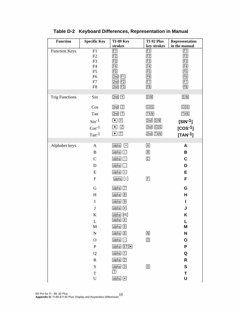
EE Pro for TI - 89, 92 PlusAppendix D: TI-89 &TI 92 Plus: Display and Keystrokes Differences
10
Table D-2 Keyboard Differences, Representation in Manual
Function Specific Key TI-89 Keystrokes
TI-92 Pluskey strokes
Representationin the manual
Function Keys F1 ƒ ƒ ƒ
F2 „ „ „
F3 … … …
F4 † † †
F5 ‡ ‡ ‡
F6 2 ƒ ˆ ˆ
F7 2 „ ‰ ‰
F8 2 … Š Š
Trig Functions Sin 2 Ú W W
Cos 2 Û X X
Tan 2 Ü Y Y
Sin-1 ¥ Ú 2 W [SIN-1]
Cos-1 ¥ Û 2 X [COS-1]
Tan-1 ¥ Ü 2 Y [TAN-1]
Alphabet keys A j Á Ñ A
B j c Ò B
C j d Ó C
D j b D
E j e E
F j Í Ô F
G j m G
H j n H
I j o I
J j p J
K j ^ K
L j y LM j z M
N j Õ N
O j | Ö O
P j § P
Q j ¨ Q
R j © R
S j ª × S
T Ü TU j « U
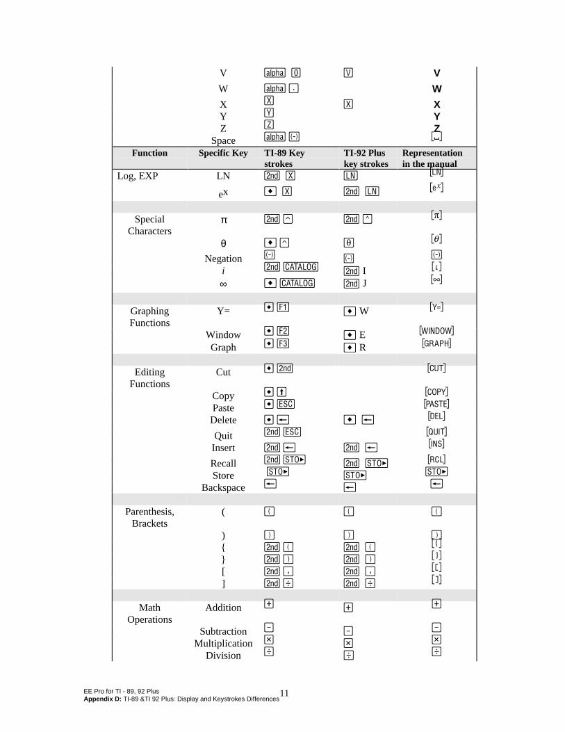
EE Pro for TI - 89, 92 PlusAppendix D: TI-89 &TI 92 Plus: Display and Keystrokes Differences
11
V j µ Ø V
W j ¶ W
X Ù Ù XY Ú YZ Û Z
Space j ·
Function Specific Key TI-89 Keystrokes
TI-92 Pluskey strokes
Representationin the manual
Log, EXP LN 2 Ù x x
ex ¥ Ù 2 x s
SpecialCharacters
π 2 Z 2 Z T
θ ¥ Z Ï Ï
Negation · · ·
i 2 ½ 2 I )
∞ ¥ ½ 2 J *
GraphingFunctions
Y= ¥ ƒ ¥ W #
Window ¥ „ ¥ E $
Graph ¥ … ¥ R %
EditingFunctions
Cut ¥ 2 5
Copy ¥ ¤ 6
Paste ¥ N 7
Delete ¥ 0 ¥ 0 8
Quit 2 N K
Insert 2 0 2 0 /
Recall 2 § 2 § £
Store § § §
Backspace 0 0 0
Parenthesis,Brackets
( c c c
) d d d
2 c 2 c [
2 d 2 d \
[ 2 b 2 b g
] 2 e 2 e h
MathOperations
Addition « « «
Subtraction | | |
Multiplication p p p
Division e e e
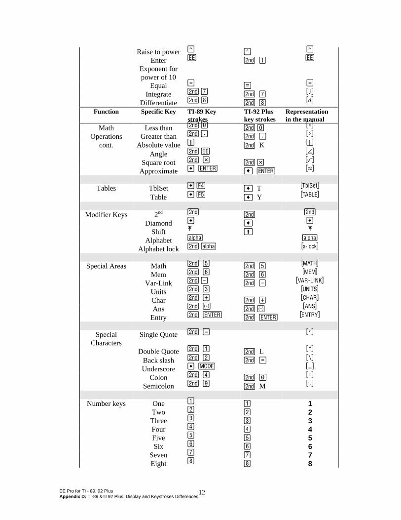
EE Pro for TI - 89, 92 PlusAppendix D: TI-89 &TI 92 Plus: Display and Keystrokes Differences
12
Raise to power Z Z Z
EnterExponent forpower of 10
^ 2 ^
Equal Á Á Á
Integrate 2 m 2 m <
Differentiate 2 n 2 n =
Function Specific Key TI-89 Keystrokes
TI-92 Pluskey strokes
Representationin the manual
Math Less than 2 µ 2 µ Â
Operations Greater than 2 ¶ 2 ¶ Ã
cont. Absolute value Í 2 K Í
Angle 2 ^ ’
Square root 2 p 2 p ]
Approximate ¥ ¥ ‘
Tables TblSet ¥ † ¥ T &
Table ¥ ‡ ¥ Y '
Modifier Keys 2nd 2 2 2
Diamond ¥ ¥ ¥
Shift Î ¤ Î
Alphabet j j
Alphabet lock 2 j ™
Special Areas Math 2 z 2 z I
Mem 2 2 ¯
Var-Link 2 | 2 | °
Units 2 ª 9
Char 2 « 2 « ¿
Ans 2 · 2 · ±
Entry 2 2 ²
SpecialCharacters
Single Quote 2 Á È
Double Quote 2 2 L É
Back slash 2 © 2 Á Ì
Underscore ¥ 3
Colon 2 y 2 Ï Ë
Semicolon 2 o 2 M Ê
Number keys One ¨ ¨ 1Two © © 2Three ª ª 3Four y y 4Five z z 5Six 6
Seven m m 7Eight n n 8
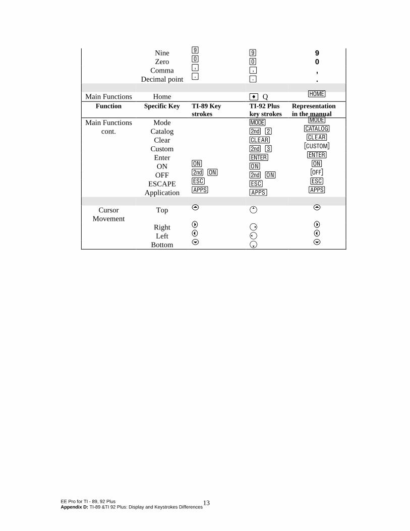
EE Pro for TI - 89, 92 PlusAppendix D: TI-89 &TI 92 Plus: Display and Keystrokes Differences
13
Nine o o 9Zero µ µ 0
Comma b b ,Decimal point ¶ ¶ .
Main Functions Home ¥ Q "
Function Specific Key TI-89 Keystrokes
TI-92 Pluskey strokes
Representationin the manual
Main Functions Mode 3 3
cont. Catalog 2 © ½
Clear M M
Custom 2 ª ¾
Enter ¸ ¸
ON ´ ´ ´
OFF 2 2 ®
ESCAPE N N N
Application O O O
CursorMovement
Top C C C
Right B B B
Left A A A
Bottom D D D
EE Pro for TI-89, 92 PlusAppendix E - Error Messages
14
Appendix E Error Messages
General Error MessagesAnalysis Error Messages
Equations Error MessagesReference Error Messages
E.1 General Error Messages
1. NOTE: Make sure the settings in the 3 screen do not have the following configuration.
Angle: DEGREE Complex Format: POLAR EE•Pro works best in the default mode settings of your calculator (ie. Complex Format: REAL , or Angle:
RADIAN ). If one of a set of error messages appears which includes “An error has occurred whileconverting....”, Data Error” , “Domain Error” , and/or “Internal Error” , check to see if the abovesettings in the 3 screen exists. If it does, change the or reset your calculator to the default mode settings
(2 ¯ ƒ ª ¸).
2. “Syntax Error ” -- occurs if the entered information does not meet the syntax requirements of the expected
entry. Check to make sure extra parenthesis are removed and the entered value meets the legal rules fornumber entry.
3. "Insufficient Table Space " or "Insufficient Memory " can occur when the system is low on available
memory resources. Consult your TI-89 manual on methods of viewing memory status and procedures fordeleting variables and folders to make more memory available.
4. The message "Unable to save EE •Pro data " will be displayed if EE•Pro is unable to save information of
its last location in the program before exiting due to low memory availability. Consult your TI-89 manualunder the index heading: Memory-manage.
5. "The variable prodata1 was not created by EE •Pro... " EE•Pro uses a variable called “prodata1” to
recall its last location in the program when it is re-accessed. If this variable list is changed to a format whichis non-recognizable to EE•Pro, it displays this message before overwriting.
6. "Data length exceeds buffer size. The variable name will be displayed instead. The variable's
value may be viewed with VAR-LINK using ˆ or recalled to the author line of the HOME
screen." 7. "An error has occurred while converting this variable's data for display . (The name of the
variable is in the title of this dialog box.) There may be something stored in the variable thatEE•Pro can't make sense of. You may be able to correct the problem by deleting thevariable ."

EE Pro for TI-89, 92 PlusAppendix E - Error Messages
15
8. “storage error...” This message is set to occur if the user attempts to enter a value into a variable which is
locked or archived, or a memory error has occured. Check the current status of the variable by pressing° and scrolling to the variable name, or check the memory parameters by pressing ¯.
9. “Invalid variable reference. Conflict with system variable or reserved name.” This can occur if
a variable name is entered which is reserved by the TI operating system. A list of reserved variable names isincluded in Appendix F.
E.2 Analysis Error Messages
AC Circuits Error Messages1. “No impedances/admittances defined” This message is displayed if an entry for impedance
ZZ_or YY_admittance is not a real, complex number or a defined variable in the Voltage Dividerand Current Divider sections of AC Circuits .
Ladder Network Error Messages1. When displaying a list of ladder network elements, an element may be named "Unknown
Element" if it contains erroneous element-type information. This may occur if the variable "ladnet",which contains information of the components and arrangement of the ladder network, has beenaltered or corrupted. View "ladnet" in °, and delete it if necessary. If deleted, the user will
need to re-enter the ladder network information.2. A dialog displaying "LadNet invalid. Delete and try again." may occur if a ladder network
contains one or more elements with erroneous data. See above.3. A dialog displaying "No ladder elements exist." will occur if an attempt is made to solve a
ladder network that contains no defined elements. Add elements to the network by pressing ‰.
4. “Invalid variable reference. Conflict with system variable or reserved name.” Thiserror is displayed if a variable name is entered as an input which is identical to a variable name usedby EE•Pro. This message is also displayed if an entered variable name is a reserved system variable.A complete list of variables reserved by the TI operating system is listed in Appendix F.
Filter Design Error Messages5. A dialog displaying " Invalid freq. ratios. " will occur if an attempt is made to design a passive
filter using frequency data that does not apply to the particular filter topology. Check your enteredvalues, you may need to try a different filter design.
Gain and Frequency: Transfer Function/Bode Diagrams6. The computed transfer function H(s) may contain “[Entry error]” rather than an actual transfer
function. This will occur when the number of zero (or numerator) terms greater than or equal to thenumber of pole (or denominator) terms.
7. An empty plot or the following dialogue may occur if an attempt is made to graph the transferfunction before one has been defined: "Undefined variable. Usually this error is caused bygraphing the Bode diagram before the transfer function Hs has been defined.F2:Analysis 5:Gain and Frequency/1:Transfer Function calculates Hs."
Computer Engineering:7. An "Invalid number format” message will be displayed if an entered number does not follow the
legal rules of the number base, or if a decimal term is entered. The format of numbers in theComputer Engineering section of EE•Pro is (p)nnnn…, where p is the letter prefix b, o, d, or hindicating binary, octal, decimal, and hexadecimal, number systems and n represents the legal digits
EE Pro for TI-89, 92 PlusAppendix E - Error Messages
16
for the number base. If a number does not begin with a letter prefix in parenthesis, then it is assumedto be in the number base set in the †/Mode dialog.
8. “Entry truncated ” will appear if an entered value exceeds the binary word size allocated in the
†/Mode dialog. For example, the decimal number 100 is expressed as a 7 bit binary
number:1100100. If a word size of 6 bits is designated in the †/Mode dialog, the latter six digits
of the number (100100) will be entered into the available word space.
Computer Engineering : Binary Arithmetic9. The message "Undefined Result" will be displayed if an attempt is made to divide by zero.
Computer Engineering: Karnaugh Map10. “Two few unique letters in Vars.” This occurs when n, the number of unique, single-letter
variables in Vars does not meet the criteria that 2n must be greater than the largest number appearingin the Minterms or Don’t Care series. Thus if the largest number is 15, there must be no less thanfour unique, single-letter variables since 24>15.
Capital Budgeting11. When changing the name of a project, the error "Duplicate project variable name." will occur if
the entered name is already in use by an existing project.12. The "Too few cash flows" message will be displayed if an attempt is made to solve a project
which contains too few or no cash flow entries.13. The message "Data Error. Reinitializing project." will occur if the project data has been altered
or is inconsistent with current state. EE•Pro will restart.
E.3 Equation Messages
If a value is entered that is inconsistent with the expected data type, an error dialog will appear which lists theentry name, the description, and the expected data type(s), and the expected units.
If an error occurs during a computation that involves temperature, "temp conversion err" or
"deg/watt conversion err" will be displayed. When solving equation sets, several messages can be displayed. These messages include: • “One or more equations has no unknowns.....” This message occurs if one or more of the
selected equations in a solution set has all of its variables defined by the user. This can be remedied bypressing N, deselecting the equation(s) where all of the variables are defined and resolving the solution
set by pressing „ twice. To determine which equation has all of its variables defined, press N to view
the equations, select an equation in question by highlighting the equation and pressing ¸, and
pressing „ to view the list of variables. A ‘é‘ next to a variable indicates a value has been specified for
that variable by the user. If all of the variables in an equation are marked with a ‘é‘, no unknown
variables exist for that equation. This equation should not be included in the solution set. Press N to
view the list of equations. Select the equations to be solved, excluding the equation with no unknowns,and press „ twice to resolve the set of equations.
EE Pro for TI-89, 92 PlusAppendix E - Error Messages
17
• "Unable to find a solution in the time allowed. Examine variables eeinput and eeprob tosee the exact statement of the problem. EE\xB7Pro sets Exact/Approx mode to AUTOduring solve.”
• “No equations have been selected. Please select either a single equation to solve byitself, or several equations to solve simultaneously.”
• "Too many unknowns to finish solving"- generally occurs if the number of equations is less thanthe number of unknowns
• "It may take a long time to find a complete solution, if one can be found at all. You may
abort the calculation at any time by pressing the ON key." -this occurs if there are manyunknowns or multiple solutions.
• “No input values provided....” occurs if none of the variables have values designated when solvingan equation set.
• "The nsolve command will be used. The existing value for the unknown, if any, will be
used as an initial guess." The nsolve function is used when a single unknown exists in the equationand the unknown variable is an input in a user defined function (an example is the error function erf inSemiconductor Basics of Solid State or the eegalv in Wheatstone Bridge in Meters and Bridges). Thensolve function will not generate multiple solutions and the solution which nsolve converges upon maynot be unique. It may be possible to find a solution starting from a different initial guess. To specify aninitial guess, enter a value for the unknown and then use F5:Opts/7:Want to designate it as the variable tosolve for. More information on the differences between the solve, nsolve and csolve functions is listed inthe TI-89 manual.
• "One complete useable solution found." All of the unknown variables were able to be solved inthe selected equations.
• "One partial useable solution found." Only some of the variables in the selected equations wereable to be solved.
• “Multiple complete useable solns found ." One or more variables in the selected equations havetwo possible values
• "Multiple partial useable solns found." One or more variables in the selected equations have twopossible values, however not all of the unknown variables were able to be solved.
The following messages can appear when attempting to graph equation set functions:
• "Independent and dependent variables are the same."• "Unable to define Pro(x)"- cannot resolve the dependent and independent variables.• "Undefined variable" too many dependent variables or dependent variable unable to be defined in
terms of the independent variable.• "Error while graphing."
E.4 Reference Error Messages
For more information, see Chapter 33, “Reference: Navigation Guide” and your TI 89 User’s Guide.
Reference : Standard Component Values
• The message "Out of range" will occur if an entered component value is not in the range of 10±23.

18
Appendix F: System Variables and reserved names
The TI-89 and TI-92 Plus has a number of variable names that are reserved for the Operating System. The tablebelow lists all the reserved names that are not allowed for use as variables or algebraic names.
Graph y1(x)-y99(x)*xt(t)-xt99(t)*ui1-ui99*tcxfactxmaxymax∆xzsc1ncontourtmintplotEstepnmax
y1’(t)-y99’(t)*yt(1)-y99(t)*xcrcyfactxsc1ysc1∆yeye0θmintmaxncurvesfldpicplotStrt
Yi1-yi99*z1(x,y)-z99(x,y)ycθczfactxridygridzmineyeφθmaxtstepdifto1fldresplotStep
r1(θ)-r99(θ)*u1(n)-u99(n)*zcncxminyminxreszmaxeyeϕθstept0dtimenminsysMath
Graph Zoom ZxminZyminZxresZtminZtmaxdeZmaxzeyeϕzpltstep
ZxmaxZymaxzθminztmaxztstepdezzsc1znmin
ZxsclZysclzθmaxztstepztplotdezeyeθznmax
ZxgridZygridzθstepzt0dezzminzeyeφzpltstrt
Statistics ü
Σx2
Σy2
medStatmedylminYregCoefSx
ý
Σxycorrmedx1medy2nStatregEq(x)*Sy
ΣxΣymaxXmedx2medy3q1seedlR2
σxσymaxYmedx3minXq3seed2
Table tblStart ∆tbl tblInputData/Matrix C1-c99 SysDataMiscellaneous Main Ok ErrornumSolver Eqn* Exp*


![INHALT - CONTENTS - MATIÈRE · RHZ(DW10ATED); (66kW-120kW) 1.6 HDi; 1.6 HDi 110; 1.6 HDi 110 FAP; 1.6 HDi 110 FAP [04]; 1.6 HDi 110FAP; 1.6 HDi 90; 1.6 HDi 90 [04]; 2.0 HDi; 2.0](https://img.pdfslide.us/doc/110x75/605cc6e9948bf00b8613e09d/inhalt-contents-matire-rhzdw10ated-66kw-120kw-16-hdi-16-hdi-110-16.jpg)


![DRAGON'S LAIR G e n e v i e v e D i d i o n K - 8 M a y 2 ... · upcoming events ee]a ee]a a ee]a a ee]a ee]a a a ee]a ee]a ee]a ee]a ee]a ee]a ee]a ee]a ee]a dragon's lair g e n](https://img.pdfslide.us/doc/110x75/5edb079c09ac2c67fa68b1f0/dragons-lair-g-e-n-e-v-i-e-v-e-d-i-d-i-o-n-k-8-m-a-y-2-upcoming-events-eea.jpg)