Embed Size (px)
Citation preview

UPS Cont.& Applications
Louis Scudiero
http://www.wsu.edu/~pchemlab; 5-2669
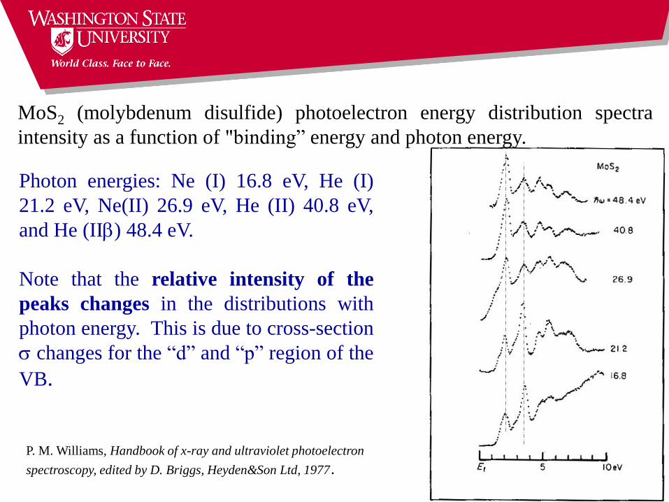
MoS2 (molybdenum disulfide) photoelectron energy distribution spectra
intensity as a function of "binding” energy and photon energy.
Photon energies: Ne (I) 16.8 eV, He (I)
21.2 eV, Ne(II) 26.9 eV, He (II) 40.8 eV,
and He (II) 48.4 eV.
Note that the relative intensity of the
peaks changes in the distributions with
photon energy. This is due to cross-section
changes for the “d” and “p” region of the
VB.
P. M. Williams, Handbook of x-ray and ultraviolet photoelectron
spectroscopy, edited by D. Briggs, Heyden&Son Ltd, 1977.
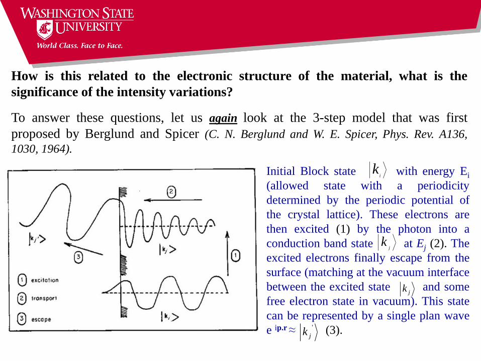
How is this related to the electronic structure of the material, what is the
significance of the intensity variations?
To answer these questions, let us again look at the 3-step model that was first
proposed by Berglund and Spicer (C. N. Berglund and W. E. Spicer, Phys. Rev. A136,
1030, 1964).
Initial Block state with energy Ei
(allowed state with a periodicity
determined by the periodic potential of
the crystal lattice). These electrons are
then excited (1) by the photon into a
conduction band state at Ej (2). The
excited electrons finally escape from the
surface (matching at the vacuum interface
between the excited state and some
free electron state in vacuum). This state
can be represented by a single plan wave
e ip.r≈ (3).
ik
jk
jk
'
jk
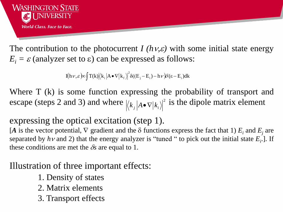
The contribution to the photocurrent I (h,) with some initial state energy
Ei = (analyzer set to ) can be expressed as follows:
Where T (k) is some function expressing the probability of transport and
escape (steps 2 and 3) and where is the dipole matrix element
expressing the optical excitation (step 1).[A is the vector potential, gradient and the functions express the fact that 1) Ei and Ej are
separated by h and 2) that the energy analyzer is “tuned “ to pick out the initial state Ei.]. If
these conditions are met the s are equal to 1.
Illustration of three important effects:
1. Density of states
2. Matrix elements
3. Transport effects
)dkE(εh)Eδ((EkAkT(k),hI iij
2
fi
2
ij kAk
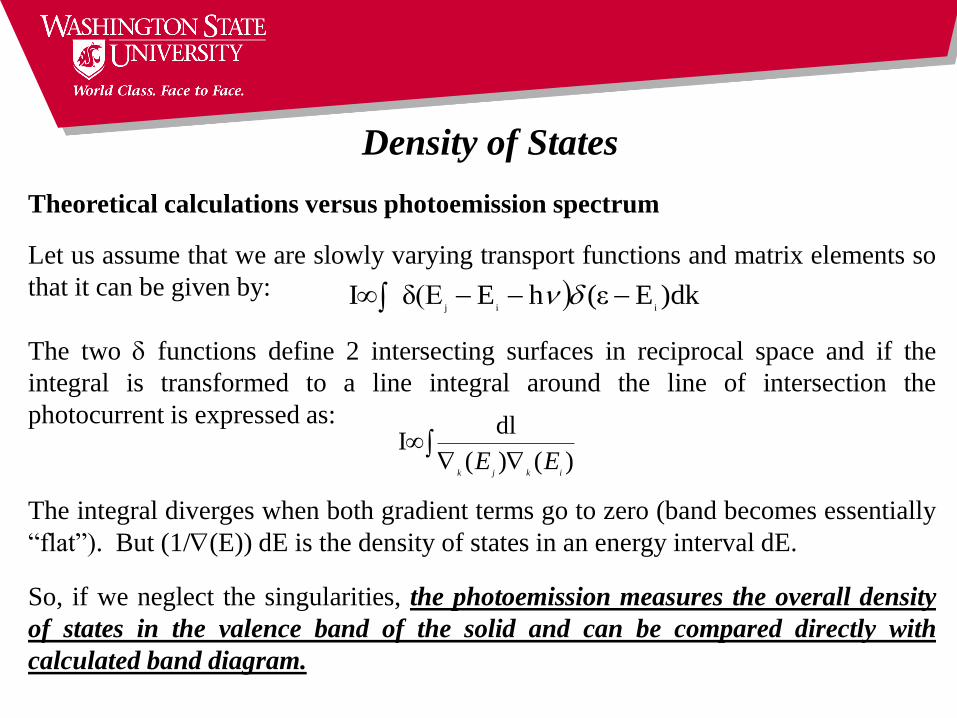
Theoretical calculations versus photoemission spectrum
Let us assume that we are slowly varying transport functions and matrix elements so
that it can be given by:
The two functions define 2 intersecting surfaces in reciprocal space and if the
integral is transformed to a line integral around the line of intersection the
photocurrent is expressed as:
The integral diverges when both gradient terms go to zero (band becomes essentially
“flat”). But (1/(E)) dE is the density of states in an energy interval dE.
So, if we neglect the singularities, the photoemission measures the overall density
of states in the valence band of the solid and can be compared directly with
calculated band diagram.
Density of States
)dkE(εhEδ(EIiij
)()(
dlI
ikjkEE
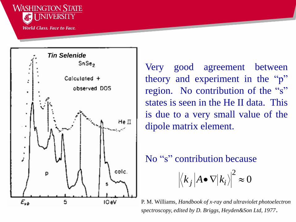
Very good agreement between
theory and experiment in the “p”
region. No contribution of the “s”
states is seen in the He II data. This
is due to a very small value of the
dipole matrix element.
No “s” contribution because
02 ij kAk
P. M. Williams, Handbook of x-ray and ultraviolet photoelectron
spectroscopy, edited by D. Briggs, Heyden&Son Ltd, 1977.
Tin Selenide
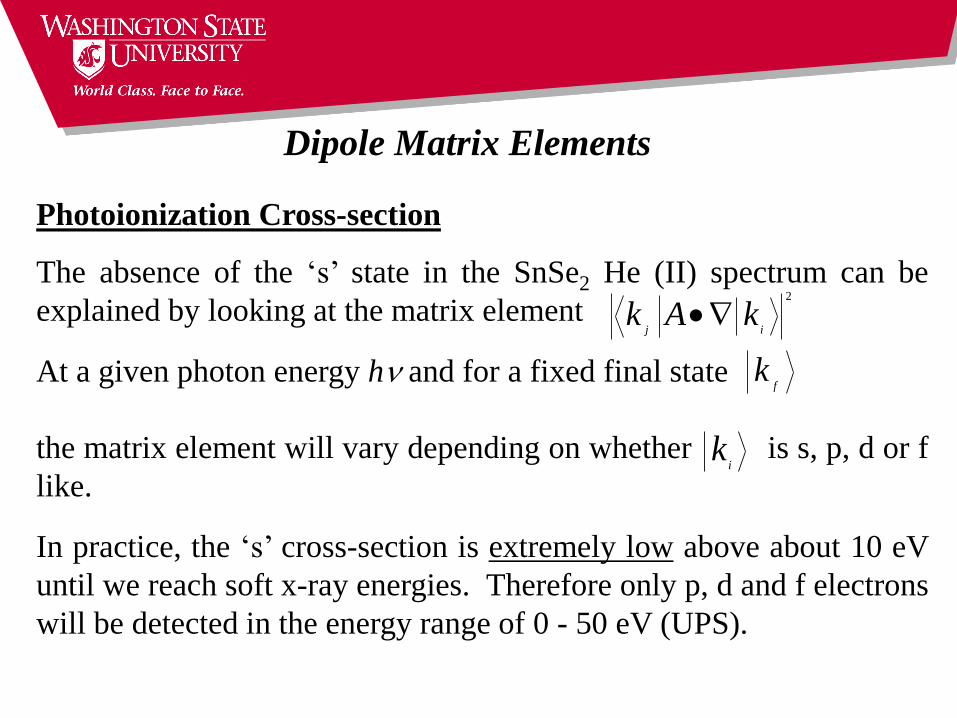
Dipole Matrix Elements
Photoionization Cross-section
The absence of the ‘s’ state in the SnSe2 He (II) spectrum can be
explained by looking at the matrix element
At a given photon energy h and for a fixed final state
the matrix element will vary depending on whether is s, p, d or f
like.
In practice, the ‘s’ cross-section is extremely low above about 10 eV
until we reach soft x-ray energies. Therefore only p, d and f electrons
will be detected in the energy range of 0 - 50 eV (UPS).
2
ijkAk
fk
ik
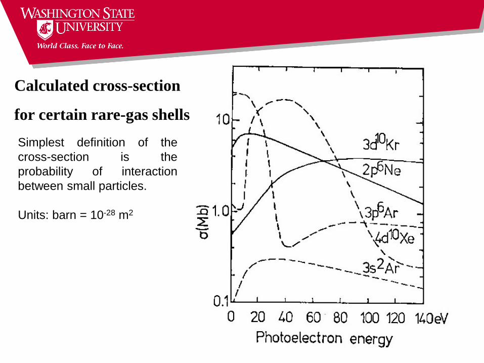
Calculated cross-section
for certain rare-gas shells
Simplest definition of the
cross-section is the
probability of interaction
between small particles.
Units: barn = 10-28 m2
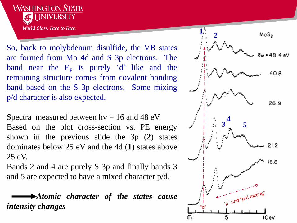
So, back to molybdenum disulfide, the VB states
are formed from Mo 4d and S 3p electrons. The
band near the EF is purely ‘d’ like and the
remaining structure comes from covalent bonding
band based on the S 3p electrons. Some mixing
p/d character is also expected.
Spectra measured between h = 16 and 48 eV
Based on the plot cross-section vs. PE energy
shown in the previous slide the 3p (2) states
dominates below 25 eV and the 4d (1) states above
25 eV.
Bands 2 and 4 are purely S 3p and finally bands 3
and 5 are expected to have a mixed character p/d.
Atomic character of the states cause
intensity changes
54
3
21
“d”
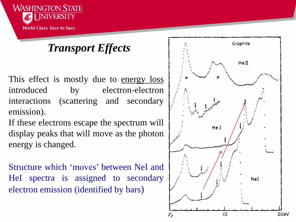
This effect is mostly due to energy loss
introduced by electron-electron
interactions (scattering and secondary
emission).
If these electrons escape the spectrum will
display peaks that will move as the photon
energy is changed.
Structure which ‘moves’ between NeI and
HeI spectra is assigned to secondary
electron emission (identified by bars)
Transport Effects
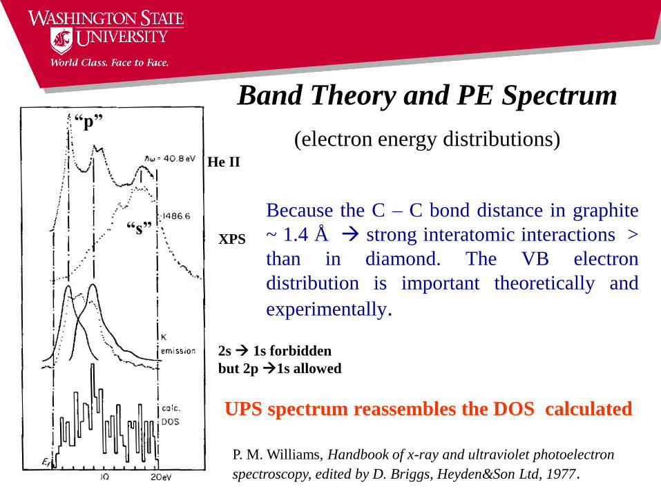
Band Theory and PE Spectrum
(electron energy distributions)
He II
“s”
2s 1s forbidden
but 2p 1s allowed
“p”
XPS
Because the C – C bond distance in graphite
~ 1.4 Å strong interatomic interactions >
than in diamond. The VB electron
distribution is important theoretically and
experimentally.
UPS spectrum reassembles the DOS calculated
P. M. Williams, Handbook of x-ray and ultraviolet photoelectron
spectroscopy, edited by D. Briggs, Heyden&Son Ltd, 1977.
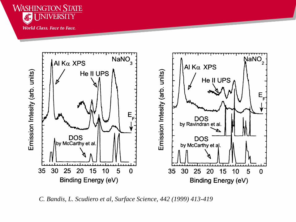
C. Bandis, L. Scudiero et al, Surface Science, 442 (1999) 413-419
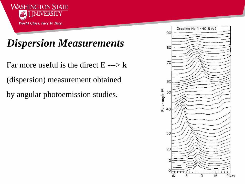
Dispersion Measurements
Far more useful is the direct E ---> k
(dispersion) measurement obtained
by angular photoemission studies.
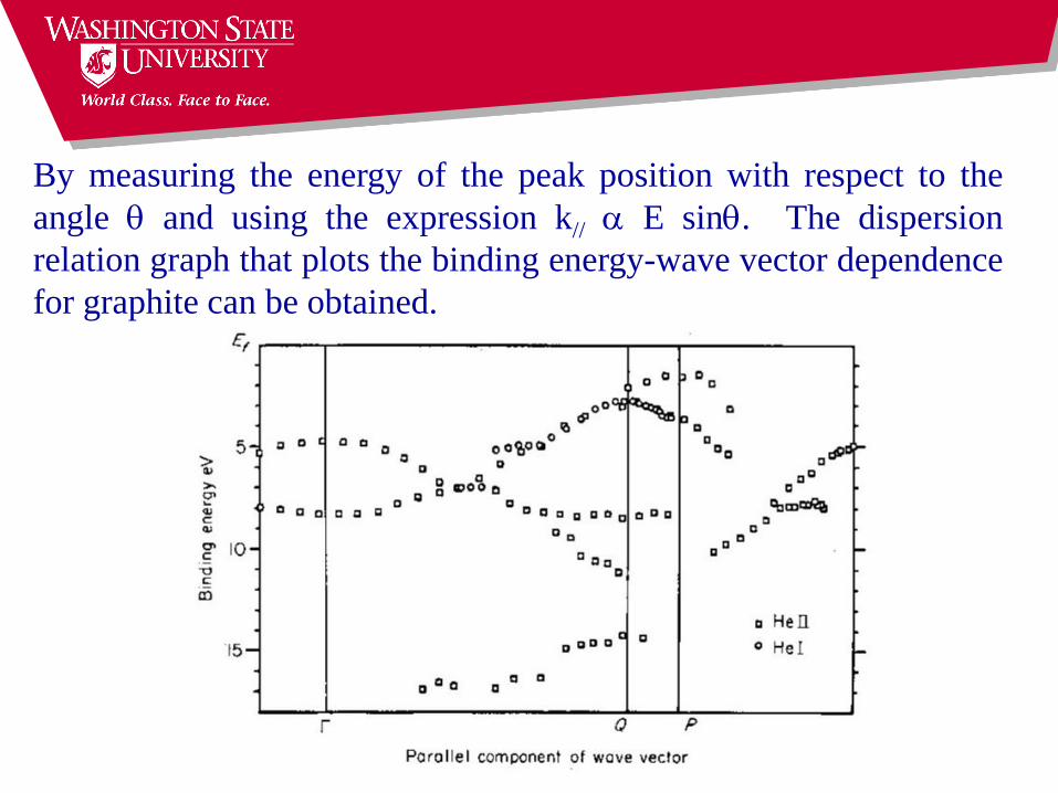
By measuring the energy of the peak position with respect to the
angle and using the expression k// E sin. The dispersion
relation graph that plots the binding energy-wave vector dependence
for graphite can be obtained.
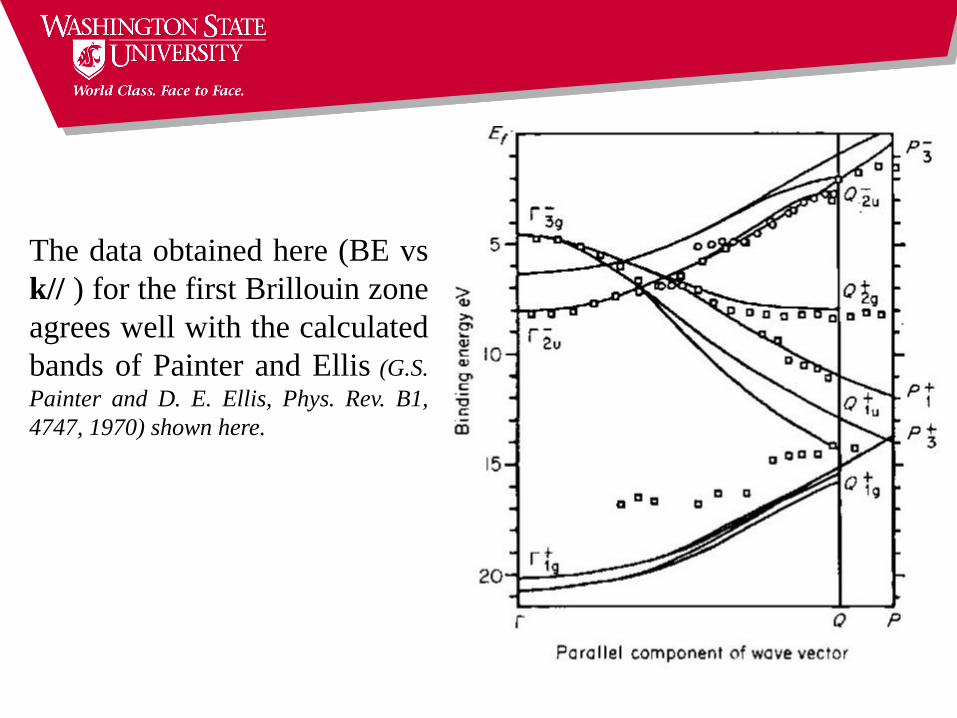
The data obtained here (BE vs
k// ) for the first Brillouin zone
agrees well with the calculated
bands of Painter and Ellis (G.S.
Painter and D. E. Ellis, Phys. Rev. B1,
4747, 1970) shown here.
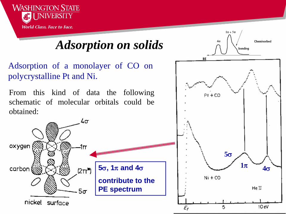
Adsorption on solids
Adsorption of a monolayer of CO on
polycrystalline Pt and Ni.
From this kind of data the following
schematic of molecular orbitals could be
obtained:
5
1 45, 1 and 4
contribute to the
PE spectrum
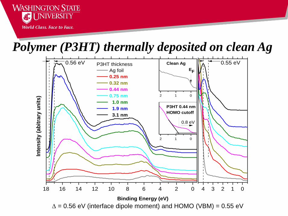
Polymer (P3HT) thermally deposited on clean Ag
18 16 14 12 10 8 6 4 2 0
2 1 0
2 1 0
Inte
ns
ity
(a
bit
rary
un
its
)
Binding Energy (eV)
P3HT thickness
Ag foil
0.25 nm
0.32 nm
0.44 nm
0.75 nm
1.0 nm
1.9 nm
3.1 nm
0.56 eV
EF
Clean Ag
P3HT 0.44 nm
HOMO cutoff
0.8 eV
4 3 2 1 0
0.55 eV
= 0.56 eV (interface dipole moment) and HOMO (VBM) = 0.55 eV
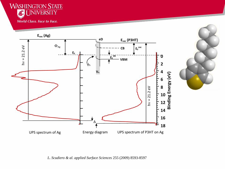
Evac (P3HT)
Bin
din
g En
erg
y (e
V)
EF
Ag
h
= 2
1.2
eV
eD Evac (Ag)
Vb
h
UPS spectrum of Ag Energy diagram UPS spectrum of P3HT on Ag
EFvac
CB
VBM
18
16
14
12
10
8
6
4
2
0 EFVB
h
= 2
1.2
eV
L. Scudiero & al. applied Surface Sciences 255 (2009) 8593-8597
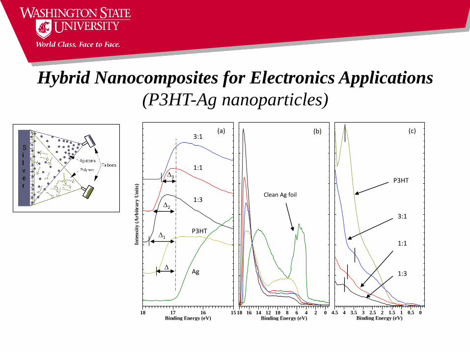
Hybrid Nanocomposites for Electronics Applications
(P3HT-Ag nanoparticles)
Washington State University --Chemistry department
Vb-a-40A/48
4.5 4 3.5 3 2.5 2 1.5 1 0.5 0Binding Energy (eV)
Washington State University --Chemistry department
Vb-matrix 3:1/5
Inte
nsi
ty (
Arb
itra
ry
Un
its)
18 17 16 15Binding Energy (eV)
Washington State University --Chemistry department
Vb-matrix 3:1/5
18 16 14 12 10 8 6 4 2 0Binding Energy (eV)
P3HT
Clean Ag foil
3
P3HT
(c)
2
1
3:1
1:1
1:3
3:1
1:1
1:3
Ag
(b)(a)
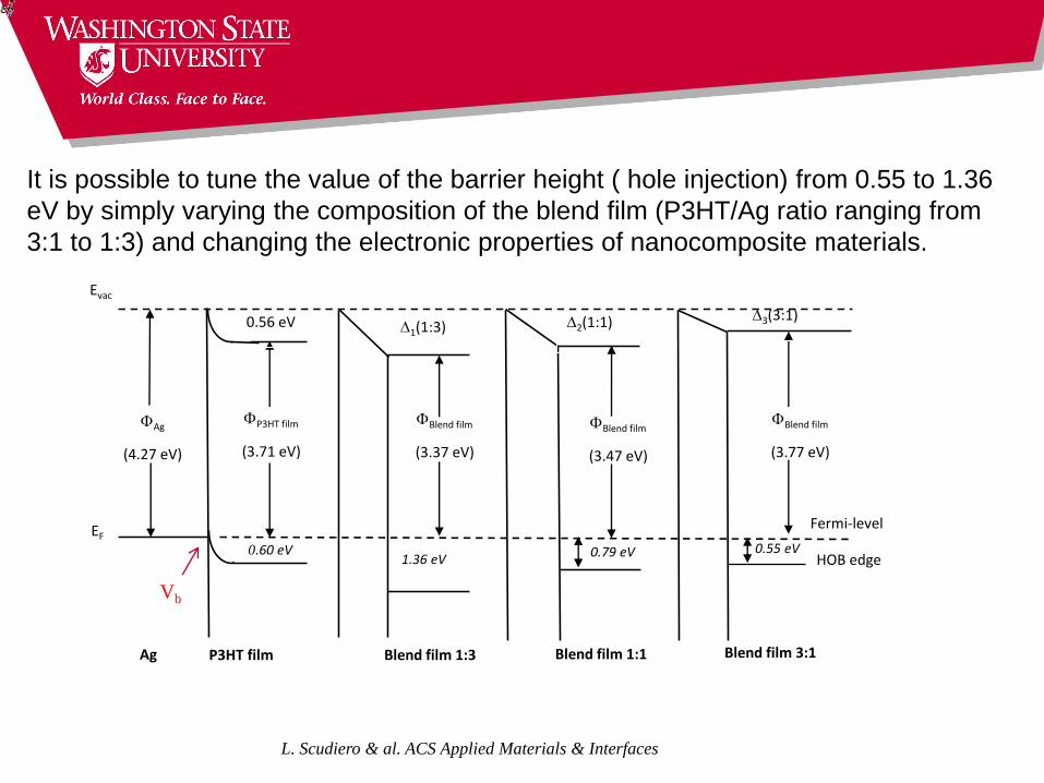
Blend film 3:1Blend film 1:1Blend film 1:3
0.55 eVHOB edge
Fermi-level
3(3:1)
Blend film
(3.77 eV)
0.79 eV
2(1:1)
Blend film
(3.47 eV)
1.36 eV
1(1:3)
Blend film
(3.37 eV)
P3HT film
(3.71 eV)
P3HT film
0.60 eV
0.56 eV
EF
Ag
Evac
Ag
(4.27 eV)
It is possible to tune the value of the barrier height ( hole injection) from 0.55 to 1.36
eV by simply varying the composition of the blend film (P3HT/Ag ratio ranging from
3:1 to 1:3) and changing the electronic properties of nanocomposite materials.
L. Scudiero & al. ACS Applied Materials & Interfaces
Vb
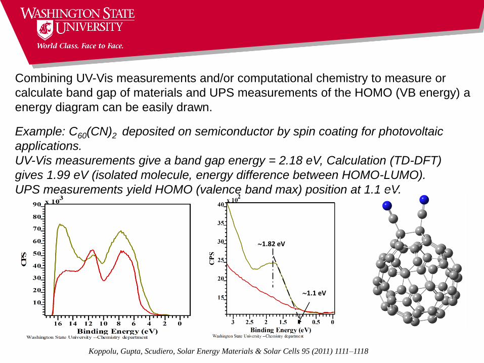
Combining UV-Vis measurements and/or computational chemistry to measure or
calculate band gap of materials and UPS measurements of the HOMO (VB energy) a
energy diagram can be easily drawn.
Example: C60(CN)2 deposited on semiconductor by spin coating for photovoltaic
applications.
UV-Vis measurements give a band gap energy = 2.18 eV, Calculation (TD-DFT)
gives 1.99 eV (isolated molecule, energy difference between HOMO-LUMO).
UPS measurements yield HOMO (valence band max) position at 1.1 eV.
1.1 eV
1.82 eV
Koppolu, Gupta, Scudiero, Solar Energy Materials & Solar Cells 95 (2011) 1111–1118
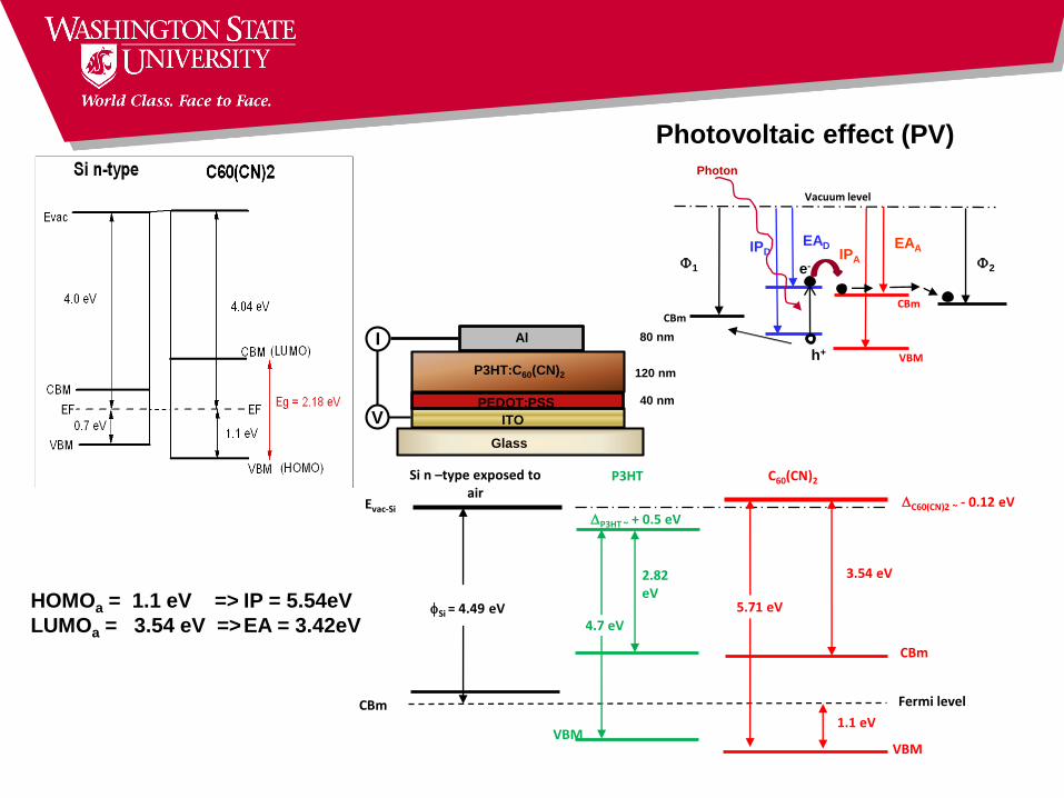
CBm
Vacuum level
VBM
CBm
1 2
IPD IPA
EAD EAA
Photon
e-
h+
VBM
P3HT C60(CN)2Si n –type exposed to air
Fermi level
Si = 4.49 eV
Evac-Si
CBm
C60(CN)2 ~ - 0.12 eV
5.71 eV
1.1 eV
3.54 eV
4.7 eV
2.82 eV
P3HT ~ + 0.5 eV
VBM
CBm
Photovoltaic effect (PV)
HOMOa = 1.1 eV => IP = 5.54eV
LUMOa = 3.54 eV =>EA = 3.42eV
Glass
ITO
PEDOT:PSS
P3HT:C60(CN)2
Al
40 nm
120 nm
80 nmI
V
UPS-HeI
DFT-GGA (generalized gradient
approximation)
d-band center
Pd
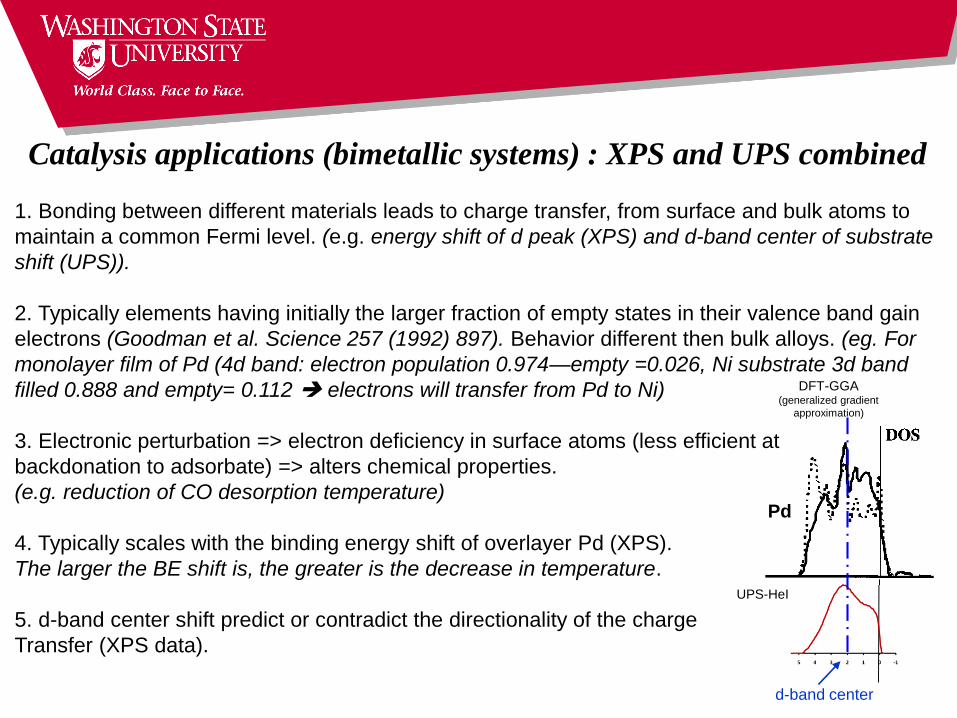
Catalysis applications (bimetallic systems) : XPS and UPS combined
1. Bonding between different materials leads to charge transfer, from surface and bulk atoms to
maintain a common Fermi level. (e.g. energy shift of d peak (XPS) and d-band center of substrate
shift (UPS)).
2. Typically elements having initially the larger fraction of empty states in their valence band gain
electrons (Goodman et al. Science 257 (1992) 897). Behavior different then bulk alloys. (eg. For
monolayer film of Pd (4d band: electron population 0.974—empty =0.026, Ni substrate 3d band
filled 0.888 and empty= 0.112 electrons will transfer from Pd to Ni)
3. Electronic perturbation => electron deficiency in surface atoms (less efficient at
backdonation to adsorbate) => alters chemical properties.
(e.g. reduction of CO desorption temperature)
4. Typically scales with the binding energy shift of overlayer Pd (XPS).
The larger the BE shift is, the greater is the decrease in temperature.
5. d-band center shift predict or contradict the directionality of the charge
Transfer (XPS data).
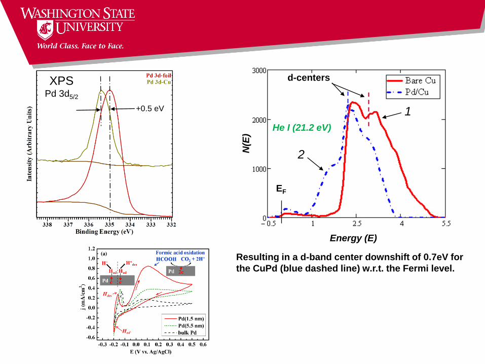
+0.5 eV
XPS Pd 3d5/2
EF
d-centers
He I (21.2 eV)
Energy (E)N
(E)
2
1
Resulting in a d-band center downshift of 0.7eV for
the CuPd (blue dashed line) w.r.t. the Fermi level.
2nd Edition E. H. Rhoderick and
R. H. Williams Oxford Science
Publications
Metal- Semiconductor Contacts
Electron states in solids and at surfaces
Density of states for n-type Si (a)
and band structure as a function of
distance (b).
The important surface parameter for
semi-conductor is the electron
affinity s defined as the difference
in energy between an electron at rest
outside the surface and an electron at
the bottom of the conduction band
just inside the surface
I is the minimum energy needed to remove an electron from the VB.gs
EI
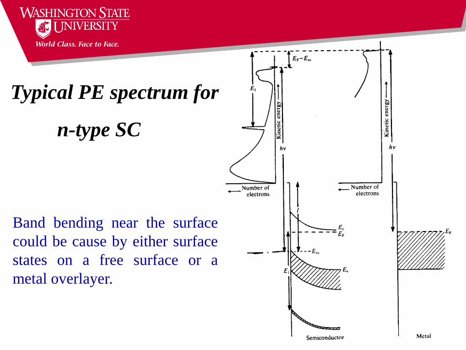
Band bending near the surface
could be cause by either surface
states on a free surface or a
metal overlayer.
Typical PE spectrum for
n-type SC
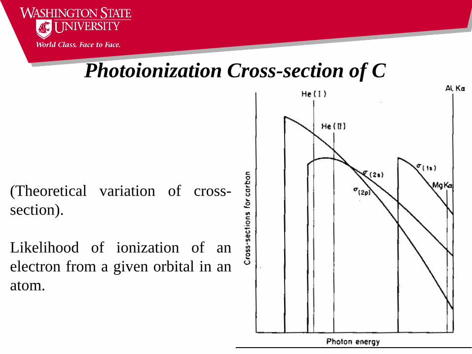
(Theoretical variation of cross-
section).
Likelihood of ionization of an
electron from a given orbital in an
atom.
Photoionization Cross-section of C
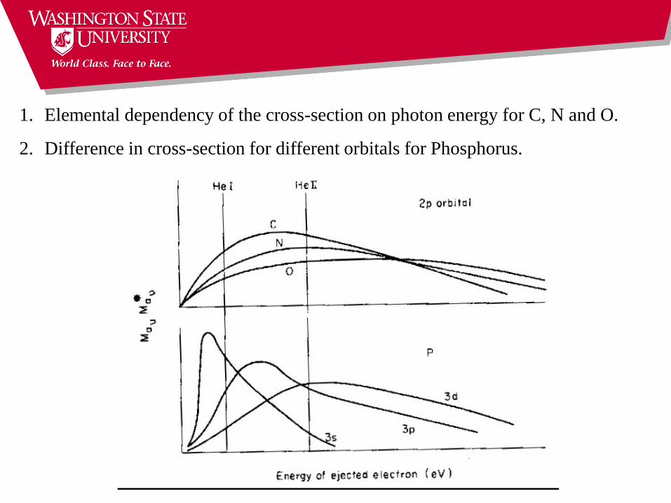
1. Elemental dependency of the cross-section on photon energy for C, N and O.
2. Difference in cross-section for different orbitals for Phosphorus.
References
• Handbook of x-ray and ultraviolet photoelectron spectroscopy,
edited by D. Briggs, Heyden&Son Ltd, 1977.
• P.M. Williams same Handbook. p.313 – 340
• M. Thompson, P.A. Hewitt and D. S. Wooliscroft same
Handbook, p341 -379
• B. L. Sharma, Plenum Press, New York