Embed Size (px)
Citation preview
UNIVERSITY OF CALIFORNIA
Los Angeles
Modification of spontaneous emission in photonic crystals
A dissertation submitted in partial satisfaction of the
requirements for the degree Doctor of Philosophy
in Physics
by
Mikhail Boroditsky
1999
ii
The dissertation of Mikhail Boroditsky is approved.
____________________________________________
Steven Kivelson
____________________________________________
Karoly Holczer
____________________________________________
Eli Yablonovitch, Committee Co-Chair
____________________________________________
Stuart Brown, Committee Co-Chair
University of California, Los Angeles
1999
iii
Table of Contents
1. INTRODUCTION............................................................................................................................... 1
2. THEORY ............................................................................................................................................. 4
3. ELECTROMAGNETIC COMPUTATIONS................................................................................. 12
4. SURFACE RECOMBINATION MEASUREMENTS ON CANDIDATE MATERIALS FOR
NANO-CAVITY LIGHT EMITTING DIODES ..................................................................................... 28
5. PHOTOLUMINESCENCE MEASUREMENTS ON PHOTONIC CRYSTALS....................... 45
6. THIN SLAB PHOTONIC CRYSTALS FOR LED APPLICATIONS......................................... 78
7. SUMMARY ....................................................................................................................................... 83
APPENDIX A: MODELING OF LIGHT-EXTRACTION EFFICIENCY OF LIGHT-EMITTING
DIODES....................................................................................................................................................... 85
APPENDIX B: ABSORPTION ENHANCEMENT IN TEXTURED AlGaAs FILMS FOR SOLAR
CELLS......................................................................................................................................................... 98
APENDIX C: SOME SOLUTIONS OF THE DIFFUSION EQUATION. ......................................... 110
REFERENCES ......................................................................................................................................... 114
Table of Figures
Figure 1. (a) A small section of an infinite dielectric slab with a triangular
array of through holes resting on a glass substrate; (b) Unit cell used for the
computation of the frequency ν vs. wave-vector k dispersion relationship.
Figure 2. Dispersion diagram of TE-like modes of the infinite photonic crystal
shown in Fig. 1(a).
Figure 3. Four different cavity configurations in the finite size photonic crystal
that were analyzed: (a) A defect is introduced by adding extra material to the
bridge between two holes; (b) A defect is introduced in the spot between three
holes; (c) The defect consists of added material in the center of a hole; (d) A
dielectric cylinder resting on a glass slab (for comparison).
Figure 4. Evolution of the localized mode frequency, effective volume and
cavity Q for the defect placed on the bridge between two holes: (a) Resonant
frequency of the mode; (b) Effective mode volume in units of (λ/2n)3;
(c) Cavity Q-factor
Figure 5. Same as Fig. 4 for the defect placed between three holes.
Figure 6. Evolution of the localized mode frequency, effective volume and
cavity Q for the defect placed on the center of a hole: (a) Resonant frequency
of the mode; (b) Effective mode volume in units of (λ/2n)3; (c) Cavity Q-
factor.
Figure 7. Mode pattern of resonant modes, in the plane of the structure, for the
modes with the smallest effective mode volume.
16
17
20
21
22
24
25
v
Figure 8. Experimental setup for photoluminescence measurements. The
absolute external quantum efficiency is measured by calibrating the measured
photoluminescence from the sample aginst the reading measured from the laser
scattered off a perfect white Lambertian reflector.
Figure 9a. The semicinductor structure corresponding to the radiative transport
model consists of a thin semiconductor film sitting on a sapphire substrate.
Figure 9b. The schematics of the AlGaN/InGaN MQW structure grown by
MOCVD on a C-plane sapphire substrate.
Figure 10. a) The InGaAlP sample consists of 0.7µm thick
In0.5(Ga0.92Al 0.08)0.5P (λ=630nm) active region doped at n=1017cm-3 level
sandwiched between n-type InAlP cladding layers grown on absorbing GaAs
substrate.b) When the top InAlP cladding layer is etched away, the
nonradiative surface recombination on the exposed surface of the active region
becomes the dominant recombination process.
Figure 11. a) An n-type In0.53Ga0.47As single quantum well structure with InP
cladding layers was grown on a InP b) A set of mesas of widths ranging from
0.12 to 2µm was etched so that the edges of the active region were exposed.
Figure 12. Inverse quantum efficiency plotted versus inverse mesa width. The
slope of the fitted line is equal to 2sτR.
Figure 13. A triangular array of holes in the thin film on InGaAs/InP double
hetero-structure.
29
31
35
39
41
42
46
vi
Figure 14. Experimental setup for angular resolved photoluminescence
measurements.
Figure 15. Experimental setup for angular resolved photoluminescence
measurements.
Figure 16. The angle of the incoming beam allows us to calculate the emission
angle from geometrical properties of the ellipse
Figure 17. Photoluminescence from a thin slab photonic crystal with a
triangular lattice. Thickness of a crystal is t=0.42nm.
Figure 18. Photoluminescence from a thin slab photonic crystal with a
triangular lattice. Thickness of a crystal is t=0.42nm.
Figure 19. Photoluminescence from a thin slab photonic crystal with a
triangular lattice. Thickness of the photonic crystal is t=240nm.
Figure 20. Photoluminescence of the bare lattice is considerably different from
that of the reference sample. PL peaks are shifted according to the lattice
constant.
Figure 21. Evolution of the spectra of the plugged lattice.
Figure 22. Shift of the photoluminescence peaks with the lattice constant.
Figure 23. Spectra of photoluminescence corresponding to sequential masks.
Figure 24. The measured bandstructure of thin slab photonic crystal with
lattice constant a=720nm and thickness t=420nm.
Figure 25. Some modes are clearly polarized while others are mixed.
Figure 26: A branch of the dispersion diagram with polarization resolution.
49
57
53
54
55
56
58
59
59
61
62
63
63
vii
Figure 27. The band structure of a plugged lattice shows nicely evolving peaks
which are nonetheless very difficult to match with the theory.
Figure 28. Experimentally measured band structure of a photonic crystal.
Lattice constant a=783nm, radius of the holes r=260nm, thickness of the slab
t=240nm.
Figure 29. Theoretical bands for the photonic crystal from Figure 28. Red lines
correspond to TM-like modes, blue lines are TE like modes.
Figure 30. Measured angular resolved spectra have relatively high Q.
Figure 31. Electric energy distribution in the Γ point of the Brillouin zone. All
energy is concentrated in the dielectric veins.
Figure 32. (a)Photoluminescence from a thin slab photonic crystal with a
triangular lattice (raw data). Thickness of the photonic crystal is t=240nm; (b)
same with efficiency calibrated to the reference sample.
Figure 33. Dependence of the Purcell enhancement factor on the value of the
non-radiative recombination rate N/R for different values external efficiency.
Figure 34. A schematic of an LED structures. Structure consists of an unetched
region surrounded by a thin slab photonic crystal which scatters guided light.
Figure 35. Spectra of the LED structure. The peak wavelength is red-shifter for
larger lattice constants.
Figure 36. Comparison of PL efficiencies from LED structures with different
lattice constants.
64
65
66
67
71
73
75
79
80
81
viii
Figures to Appendices:
Figure A1: (a) Transmission of light within the escape cone. (b) In the
presence of an anti-reflection coating, there are two successive escape cones,
but net escape angle is the same as in (a).
Figure A2: The total efficiency is the product of the internal quantum
efficiency times the light extraction efficiency. However the light extraction
efficiency is itself dependent on the internal quantum efficiency due to the
inevitable re-absorption of some of the light. In thin LED’s the re-absorption
effect is less severe.
Figure A3: The extraction efficiency versus LED chip height. For the highest
internal quantum yield (IQE) material, the LED should be a thin film, but for
lower IQE a thick LED is better because the light escapes more readily from
the edges.
Figure A4: Scaling properties of the light extraction efficiency.
Figure A5: Dependence of light extraction efficiency on position of the active
layer for a device with a sheet bottom contact and a small circular top contact.
Figure A6: Monte-Carlo results. Top and side views of light escaping from an
LED. The white areas have more light emission than the dark ones.
Figure A7: Variation of the size around commercial dimensions.
Figures A8(a,b) : Effect of additional texturing on light extraction efficiency.
86
91
92
93
93
94
95
96
ix
Figure B1: Variation of sphere density with angular velocity. The
concentration of polystyrene spheres solution in methanol solution is 1.5% by
weight. The darker area represents spheres. A) Sphere distribution for 1800
rpm; B) Sphere distribution for 1700 rpm; C) Sphere distribution for 1600 rpm;
D) Sphere distribution for 1550 rpm.
Figure B2: Experimental configuration and definition of the variables used in
the modeling.
Figure B3: Sample with the sparse distribution of spheres. The light trapping
absorption enhancement effect is minimal.
Figure B4: Sample with 50% of the surface area covered with spheres. A large
absorption enhancement is obtained near the band edge.
Figure B5: Comparison between the theoretical absorption for an optically
textured film and the best values obtained experimentally.
Figure C1: The carriers are generated close to the surface with surface
recombination velocity S and diffuse towards the quantum well.
Figure C2: Carrier are injected uniformly, and can either recombine radiatively
in the bulk or non-radiatively at the surface.
100
101
104
105
106
108
110

Acknowledgements
The author is very grateful to everyone he worked with during this project and discussed
its various aspects. Special thanks to Roberto Coccioli for help with computer
simulations, Thomas Krauss for nanofabrication, and Rutger Vrijen for help in
measurements. Different stages of this work were supported by ARO, NSF, and Hewlett-
Packard MICRO grants.
xi
VITA
10/09/68 Born
03/93 M.S. in Physics, St. Petersburg Technical University
12/96 M.S. in Physics, University of California Los Angeles
10/94-04/96 Teaching Associate
10/94-12/98 Graduate Research Assistant,
University of California Los Angeles
xii
Publications and Presentations
M. Boroditsky, R. Ragan, E. Yablonovitch, "Absorption enhancement in Ultra-
thin textured AlGaAs films", to be published in Solar Energy and Solar Cell Materials.
M. Boroditsky, R. Coccioli, E. Yablonovitch, “Analysis of photonic crystals for
light-emitting diodes using the finite difference time domain technique”, Proceedings of
Photonics West ’98, San Jose, CA, Jan 20-24, 1998 (in print)
M. Boroditsky, E. Yablonovitch, ”Spontaneous Emission Engineering in Light
Emitting Diodes”, Proceedings of LEOS ’97, 2, p 7.
M. Boroditsky, E. Yablonovitch, “Photonic Crystals Boost Light Emission”,
Physics World, July 1997, p.53.
M. Boroditsky, E. Yablonovitch, “Light extraction efficiency from light-emitting
diodes”, SPIE, 3002 (1997), p.119-22.
M. Boroditsky, E. Yablonovitch “Light extraction efficiency from visible light-
emitting diodes”, Conference on Lasers and Electro-Optics, Technical Digest Series,
9 (1996), p.141-2.
M.L.Boroditsky, A.E.Dul`kin, I.V.Kochnev, D.A.Livshits, N.O.Sokolova,
E.U.Rafailov, I.S.Tarasov, Yu.M.Shernyakov, B.S.Yavich. “High Power Single-Mode
InGaAsP/GaAs Lasers (λ=0.98mm) MOCVD grown,” Pis`ma v ZhTF, 20(6), pp.62-66
(1994).
M.L.Boroditsky, D.Z.Garbuzov, A.Y.Gorbachov, N.D.Ilinskaya, D.A.Livshits,
D.N.Marinsky, E.U.Rafailov, A.L.Stankevich, I.S.Tarasov. “High Power Single-Mode
Buried InGaAsP/GaAs SC DHS Lasers,” Pis`ma v ZhTF, 19(21), pp.78-81 (1993).
xiii
M.L.Boroditsky, D.Z.Garbuzov, D.A.Livshits, E.U.Rafailov, “Mode composition
control in high power buried InGaAsP/GaAslasers”, SPIE's OE/LASE '94, January 22-29,
1994, Los-Angeles.
R. Coccioli, M. Boroditsky, K. Kim, Y. Rahmat-Samii, E. Yablonovitch, “What
is the Smallest Possible Electromagnetic Mode Volume in a Dielectric Cavity?” to be
published in IEE Proceedings – Optoelectronics, January 1999.
R. Coccioli, M. Boroditsky, E. Yablonovitch, T. Itoh, “Planar Geometry
Electromagnetic Crystals for Optical and Millimeter-Wave Applications” (invited)
International workshop on Contemporary Photonic Technology, January 12-14, 1999,
Sendai Japan.
D. Garbuzov, G.-J. Shiau, V. Bulovic, M. Boroditsky, C.-P. Chao, S.R. Forrest,
“Photoluminescence study of excess carrier spillover in 1.3 µm wavelength strained
multi-quantum-well InGaAsP/InP laser structures,” Applied Physics Letters, 66, (1995),
p.1307.
D.Z.Garbuzov, M.L.Boroditsky, N.D.Il'inskaya, D.A.Livshits, D.N.Marinskiy,
E.U.Rafailov, “Controlling the mode composition of high-power buried InGaAsP/GaAs
lasers with a wavelength of 0.8µm,” Semiconductors 28(2), pp.191-194 (1994).
T. Krauss, M. Boroditsky, R. Coccioli, O. Painter, A. Scherer and E.
Yablonovitch, "Photonic crystal microcavity enhanced LEDs", CLEO/Europe, Paper
CWA4, Glasgow, September 1998.
xiv
ABSTRACT OF THE DISSERTATION
Modification of spontaneous emission in photonic crystals
by
Mikhail Boroditsky
Doctor of Philosophy in Physics
University of California, Los Angeles, 1999
Professor Eli Yablonovitch, Co-chair
Professor Stewart Brown, Co-Chair
The modification of spontaneous emission in a semiconductor photonic crystal
and in a semiconductor microcavity at room temperature is the subject of this thesis. The
broad spectral linewidth of semiconductors together with large surface recombination
velocities make the observation of these effects an interesting and challenging task.
A quantum electrodynamical model is used to estimate enhancement of
spontaneous radiation rates in photonic crystals and microcavities. Extensive numerical
computations were employed to calculate the band structure of thin slab photonic crystals
and the properties of microcavities. The minimal achievable effective mode volume, a
xv
crucial parameter for cavity enhancement of spontaneous emission was shown to be
§λ/2n)3 where λ is the resonant wavelength and n is the refractive index. Five-fold
enhancement of spontaneous emission was shown to be physically possible in InGaAs
nanocavities.
Photoluminescence measurements of surface recombination velocity were used in
the search of material system most suitable for fabrication of such a photonic crystal. The
InGaAs and InGaN material systems were shown to be good candidates for luminescent
photonic bandgap structures.
Angular resolved photoluminescence measurements were used to experimentally
measure the band structure of so-called electromagnetic conduction bands of such a
photonic crystal.
The enhancement of spontaneous emission extraction from a thin slab photonic
crystal was demonstrated. It was shown that emission into the leaky bands of the
photonic crystal has the same benefit as cavity-enhanced spontaneous emission, provided
these bands are flat enough relatively to the spectral emission bandwidth of the material.
Recommendations for novel LED designs were worked out based on the results of this
study.
1
1. Introduction
For a long time the spontaneous emission rates were believed to be an intrinsic
property of a material. It was later understood that spontaneous emission also depends
strongly on the surrounding environment through the density of states and local strength
of the electromagnetic modes1. First works on enhancement and suppression of
spontaneous emission in the microwave regime were performed in 1980’s by Haroche
and Kleppner2.
It was predicted by Purcell3 that an atom in a wavelength-size cavity can radiate much
faster than in the free space. This effect was measured in a cavity formed by two parallel
mirrors by Haroche et al.4. All these measurements were performed on single atoms. A
similar effect can be observed in semiconductor materials, even though a smallest chunk
of the semiconductor we can imagine consists of thousands of atoms. Enhancement of the
spontaneous emission rate was recently observed at low temperature in Vertcal Cavity
Surface Emittin Laser (VCSEL) structures of small lateral dimensions5.
Photonic crystals, artificially created, multi-dimensionally periodic structures are
known for a forbidden electromagnetic bandgap. For that reason, they can be used to
modify spontaneous emission. Initially, it was proposed to use photonic crystals to inhibit
spontaneous emission6, but they can be employed to enhance it as well.
Modification of spontaneous emission in photonic crystal and enhancement of
spontaneous emission in a semiconductor microcavity making use of photonic crystal at
room temperature is the subject of this thesis.
2
In the second chapter the quantum theory of spontaneous emission will be
presented. The behavior of an atom in a cavity will be discussed, and Purcell's
enhancement factor will be re-derived for the particular case of the quantum well active
material in a microcavity.
Electromagnetic simulations of photonic bandgap materials will be discussed in
the third chapter including band structure calculations and the study of defect modes.
Enhancement of the spontaneous emission rate in the resonant mode of a microcavity is
inversely proportional to the volume occupied by this mode. This makes cavity
optimization an important part of this project, requiring extensive numerical work. It will
be shown that a single-mode nanocavity can be built with semiconductor material with
cavity volume as low as ≈2(λ/2n)3, where n is the refractive index of the semiconductor,
and λ is the resonant wavelength.
Observation of spontaneous emission from such cavities require relatively low
non-radiative surface recombination. Identification of suitable material systems using
photoluminescence measurements on samples with exposed edges is described in detail
in the fourth chapter.
Chapter five of the thesis is about photoluminescence from photonic crystals
without nanocavities. The relative frequency of the photonic and electron bandgap is
shown to change the photoluminescence spectrum and directionality of the spontaneous
emission from the sample compared to an unetched reference sample.
3
The results of photoluminescence measurements on thin film photonic crystal will
be presented in the chapter five. In this way, the band structure of the photonic crystal can
be directly measured.
Enhancement of spontaneous emission from the nanocavities is of considerable
practical interest. Indeed, Light-Emitting Diodes (LED's) are a class of opto-electronic
devices based on spontaneous electron-hole recombination in semiconductors. The
biggest problem in design of such a device is the difficulty of extracting light from the
high-refractive index material. The principle of resonant-cavity enhancement can be used
to enhance light emission. The use of one-dimensional Distributed Bragg Reflectors to
realize high efficiency planar microcavity LEDs was proposed by F. Schubert et al .7, and
was most successfully realized by De Neve et al.8. However, only three-dimensional
cavities can provide a really significant improvement in the light extraction. We will
show in chapter five that even though a five-fold spontaneous emission enhancement is
possible in a 3-d nanocavity, a similar enhancement can be obtained from a thin slab
photonic crystal, if the spontaneous emission from the active material is tuned to the
leaky conduction bands of the photonic crystal.
Thin film photonic crystals are also a possible tool for efficient light extraction.
We studied the external scattering of guided waves by photonic crystal and their potential
application in the light-emitting diodes in the chapter six.
4
2. Theory
2.1. Two-level systems
Spontaneous recombination in semiconductors is a complicated process. The
consideration of a simple two level system gives many good insights into this process.
Downward transition in a simple two-level system can be spontaneous or stimulated. It is
easy to see that spontaneous emission accounts for most of the radiative recombination in
thermal equilibrium at room temperature. Indeed, the detailed balance for such a system
is:
0)()( 221022101121 =++−= NANBNBN ωρωρ . (1)
A12 and B21 and are Einstein's coefficients and ρ(ω) is the density of electromagnetic
modes.
Using B12=B21 and TeN
N /
2
1 ω!−= we get
30/
221
0221 ~1
1)(
sSpontaneou
Stimulated −
−== e
eNA
NBTω
ωρ!
, (2)
with kT=0.27eV and hω=1eV. So the world we live in is mostly the world of
spontaneous emission and it is interesting to see if we can tailor the properties of this
process according to our needs.
2.2. Quantization of the electromagnetic field
Quantization of the electromagnetic field is necessary for a correct understanding
of the nature or spontaneous emission and its engineering. The quantization procedure in
5
the case of a media with a non-uniform distribution of the dielectric constant ε(r) is the
same as for the free space, but the vector potential operator A(r,t) does not consist of
plane waves anymore.
The classical Maxwell equations
01
01
0))()((
0
=∂∂−∂×∇
=∂∂+×∇
=⋅∇
=⋅∇
t
E
cB
t
B
cE
rEr
B
&&
&&
&&&
*
ε
(3)
can be transformed by introduction of a vector-potential A&
such that t
A
cE
∂∂−=&
& 1 and
AB&&
×∇= . It yields the wave equation in the form of
0)( 2 =−∇−∇∇ AkAA&&&
ε (4)
In the case of the uniform dielectric constant, its solutions are plane waves, however,
these solutions can be quite complicated function in the arbitrary cases. Nonetheless, the
canonical quantization procedure still can be applied by the introduction of operators
satisfying the commutation relations.
Then, the operator of the vector-potential for a given mode becomes
)]()()()([2
),( *00
2 21
rAtarAtac
trA&&&&!&&
++
=
ωπ
(5)
where operators a(t) and a+(t) are photon annihilation and creation operators
correspondingly, and A0(r) describes the spatial distribution of the classical eigenmode of
6
frequency ω. Operators of electric and magnetic fields are readily derived from the
definition of A(r,t):
( ))(),(
.].)()([2),(
0
02
1
rAtrB
ccrAtaitrE&&&&
&!
&&
×∇=
−= ωπ. (6)
Obviously, for any state with n photons the diagonal matrix elements of the
electromagnetic field operators are equal to zero:
0)()( == nrBnnrEn&&&&
(7)
While diagonal matrix elements of the square of the electric field is
)()(4)( 21
2
02 += nrAnrEn
&&!
&&ωπ , (8)
and can be rewritten as a sum of a classical part, corresponding to n photons in the mode
and a purely quantum mechanical contribution, called also zero-point fluctuations of the
field:
0
22
02 )()(4)( rEnrAnrEn
&&&&!
&&+= ωπ . (9)
That means that even when the system is in the state with no photons, the net mean
square fluctuations of the electric field are not zero.
The Hamiltonian HF of the electromagnetic field becomes that of a harmonic oscillator
after we plug Eq (6) into )(8
1 ++ += HHEEHπ
:
)( 21+= +aaH F ω! . (10)
If we work with a classical multi-mode system, its quantum Hamiltonian is just a sum
over allowed electromagnetic modes, including the polarization:
7
∑ ++
=
nnn rAtarAta
ctrA )]()()()([
2),( *
2 21
&&!&
ωπ
(11)
In this way the Hamiltonian of the field becomes a sum of the photon energy in all
modes. Importantly, from the viewpoint of spontaneous emission, even when the average
electric field is zero when there are no photons in the mode, the mean square of the
electric field is not zero but equals to 2
0212 )(4)( rAnrEn
&!
&&ωπ= . That is we can say
that fluctuations in the mean square of the field are distributed in the same way as the
classical field.
Many important features of spontaneous emission in semiconductors can be obtained
from the analysis of a two level system coupled to one or many electromagnetic mode(s).
For a single mode system:
],][[021 +++ −+++= σσωσω aaCiaaH z !!! (12)
The coupling constant 12
21
12
21
0
2ˆ2d
Vxe
VC
&
!
&
!
≈Ε⋅
=
ωπ
ωπω is Rabi frequency and it
sets an important time scale in the atom-light interaction.
For the near-resonant interactions, the rotating wave approximation can be used. The
higher order terms (the ones that do not explicitly preserve the energy of the system) are
omitted and the Hamiltonian can then be diagonalized:
],[021 +++ −++= σσωσω aaCiaaH z !!! (13)
The solution for the simplest case when ω=ω0 is so-called vacuum Rabi oscillations, that
is a photon is emitted into the modes and then reabsorbed and re-emitted again.
8
When the atom is coupled to a continuum of modes, so that the interaction Hamiltonian is
,][,
,,int ,∑ ++ −=λ
λλ σσλ
kkk aaCiH
k! then the exited state 0002 ,..,, shows exponential
decay 3
2
1230
212 3
4 where,)( 21
c
dAetP tA
!
&ω
== − , which is exactly the classical expression
for the spontaneous emission rate. It's interesting to see that this emission rate can be
found approximately from dimensional considerations as A21~C2ρ(ω).
For a dipole located at the arbitrary point r of the mode, the transition rate would be
VrAc
dnrA
2
03
32
12 )(3
4)(
&
!
& ω= (14)
with normaization 1)()( 32
0 =∫ rdrAr&
ε .
Placing an atom in a lossy (leaking or absorbing) cavity can produce different
effect on the spontaneous emission process. The cavity by itself brings in another time
scale 0ω
τ Qav = describing the photon lifetime in the cavity, with Q being the quality
factor of the cavity and ω0 being its resonant frequency. Depending on the relation
between the cavity lifetime, and the vacuum Rabi oscillations period in the same cavity
without losses there can be two simple extreme cases:
τ>>tR Damped Rabi oscillations
Leakage from the cavity is much slower then the Rabi oscillation so that the exponential
decay is an envelope for the Rabi oscillations: CePt
Q2
2 cosω−
=
9
τ<<tR Overdamped cavity (E.Purcell, 1946)
This case is of special interest for us, so we will derive recombination rate below and
then will apply the results to the semiconductor's emission in order to estimate the
maximum achievable spontaneous emission enhancement in a dielectric microcavity.
2.3. Purcell effect
The Purcell enhancement factor2 needs to be modified when considering generation of
light in semiconductor quantum well (QW) structures.
The classical electric field of the cavity mode)(rE has to be normalized EE α→
with the normalization factor α so that
( )2
)()(41 032 ωαεπ
!=∫ rrEr d , (15)
where ε is the material dielectric constant and ω0 is the resonant frequency of the cavity.
This gives the normalization factor
∫=
rrEr 3202
)()(
2
dεωπα !
(16)
In the above equations the integration extends over the quantization volume. The
spontaneous emission rate at frequency ω, into the resonant mode cantered at ω0, at a
given point r , follows from Fermi’s golden rule and equals to
( )))2/()((2
)(2
)( 220
2
ωωωπωαπ
∆
∆
+−⋅=Γ
!!
grEdr , (17)
10
where d denotes the atomic moment dipole, ∆ω is the cavity linewidth, and g is the
degeneracy of the cavity mode. The last term in Equation (17) represents the Lorentzian
lineshape of electromagnetic modes – there are g modes in the frequency range ∆ω. The
dot product (d⋅αE(r )) has to be averaged over the possible orientations of the atomic
dipole moment. At this point we need to take the specific account of optical transition in
semiconductor quantum wells. First, electron-heavy hole transitions are the major
contributor to the spontaneous emission. Second, these transitions are only allowed if the
dipole moment of the transition lies in the plane of the quantum well, so that
<dx2>=<dy
2>=d2/2, <dz2>=0. Then, if the mode’s electric field is also in the QW plane, as
happens for TE modes, the average ( ) 222))(()2/1()( rEdrEd αα =⋅ . Note that in the
case of bulk semiconductor, or for interaction with random modes, the pre-factor above
would have been 1/3.
If the active material is placed in the point of maximum electric field of the mode,
the emission rate is
( )))2/()((22
222
0
2max
2
ωωωπωαπ
∆
∆
+−=Γ
!!
gE
d(18)
If the linewidth of the cavity ∆ω is much smaller than emission spectrum width of
the active material ∆ωm, integration over the frequencies leads to
( )m
g
ωαπ
∆=Γ
!!
2max
2
2
2E
d (19)
Plugging in the value of the normalization factor α2 gives
11
∫∆=Γ
rrEr
Ed32
2max
220
)()(
2
d
g
m επ
ωω
! (20)
The unenhanced spontaneous emission rate in the bulk can be calculated using the
classical formula9
3
32
3
32
03
84
3
4
λπω
!!
dd n
c
n ==Γ (21)
Thus, the overall enhancement factor, which can be used as a figure of merit for
optimization of a resonant-cavity structure becomes
∫=
ΓΓ
rrEr
E32
2max
3
0 )()(16
3
dngQm επ
λ, (22)
where we callm
mQωω
∆= 0 is the material quality factor. Introducing the mode volume Veff
( )max2
32
)()(
)()(
rEr
rrEr
ε
ε∫=d
Veff, (23)
the enhancement of spontaneous emission rate can be recast in the following form:
( )eff
m
V
ngQ
πλ
2
2/3 3
0
=ΓΓ
(24)
This expression differs from the one originally derived by Purcell by a degeneracy factor
g and a factor of π/4 which follows from integrating over the Lorentzian cavity lineshape,
and polarization averaging in the quantum well structures.
It will be shown in chapter 5, surprisingly, that a plain photonic crystal without any
nanocavities gives rise to the same effect. This requires weak dispersion of the photonic
conduction bands, and their coupling of spontaneous emission to external plane waves.
12
3. Electromagnetic computations
The spontaneous emission rate of an atom can be increased or decreased by changing its
environment. It has been known since 1946 that the enhancement of spontaneous
emission rate, or Purcell effect, can be achieved in very tiny electromagnetic cavities10. It
is tempting to apply the Purcell effect to the spontaneous emission of opto-electronic
materials11, such as III-IV semiconductors. Several examples has recently appeared: a
five-fold increase in the radiative rate was demonstrated at low temperatures in VCSEL-
type micro-cavities by Gerard et al5. Likewise, layered 1-dimensional Bragg micro-
cavities increase the efficiency of planar light emitting diodes (LED’s) as proposed by F.
Schubert et al .7, and most successfully realized by De Neve et al8. It was shown in the
chapter 2 that the enhancement of spontaneous emission rate in a semiconductor
nanocavity structure with a quantum well active region is:
( )effV
nQgπλ
22/3 3
0
=ΓΓ
, (25)
where Q is the quality factor of the cavity, n is the refractive index of the semiconductor,
λ is the mode’s wavelength, g is the mode degeneracy factor, and Veff is the mode
volume defined as
( )max2
32
)()(
)()(
rEr
rrEr
ε
ε∫=d
Veff. (26)
The integration in Equation (26) is performed over the quantization volume.
13
It is possible to build a very high Q dielectric cavity using photonic crystals, but once the
spectral width ∆ν= ν/Q of a resonant cavity is smaller than the spontaneous emission
linedwidth ∆νm there is no further significant increase in the spectrally integrated
spontaneous emission rate. The normal spontaneous emission bandwidth of opto-
electronic semiconductors at room temperature limits the useable cavity Q to Q>10 or
Q>40 depending on the specific material. Looking at Equation (26), a significant
enhancement of spontaneous emission rate in semiconductors at room temperature
requires building the smallest possible electromagnetic cavities, or, in other words,
reducing the effective volume Veff . This makes the search for the smallest mode volume
achievable with the dielectric material an important question. The value of
Veff=2.55(λ/2n)3 was previously reported by Foresi et al.12,13 for a 1-dimensional bridge
photonic crystal. Is it possible to do better?
The minimal size of a dielectric cavity mode is the subject of this chapter. We have used
the Finite Difference Time Domain (FDTD) method to compute the smallest achievable
effective volume. The FDTD method has been chosen, among the many available,
because of its capability to deal with complicated structures such as those analyzed here.
Using different kinds of boundary conditions, the method allows one to deal with many
different types of problems: computation of the dispersion diagram, computation of
resonant frequency, effective mode volume, Q, and mode pattern in the nanocavity.
FDTD was used by Sakoda14 to study modal properties of defects in infinite 2D photonic
crystals without considering mode volume. Indeed, the method proved to be very
effective in this calculation because it provides a wealth of data from which it is possible
14
to derive all the quantities of interest for the design of nanocavities. The code
implemented in our work has been extensively tested against data available in the
literature. Using this valuable numerical tool, we will show that an effective volume as
low as Veff ≈2(λ/2n)3 is achievable. As a complementary result, Painter et al.15 have
demonstrated that very high Q≈4000 can be achieved in similar thin-slab PBG cavities at
the price of slightly larger mode volume.
We have thoroughly analyzed numerous possible configurations of the dielectric cavity
created by introduction of a defect into a 2-dimensional photonic crystal. Our baseline
2-D photonic crystal consisted of a thin slab with a triangular array of holes. Our choice
of such a structure in Fig. 1(a) is justified by the following considerations: This type of
2-D photonic crystal structure shows a large bandgap for TE polarization, providing good
horizontal confinement. Guided modes in such a structure are well confined vertically by
the slab refractive index and total internal reflection, so the vertical dimension of the
mode is small. This structure is much easier to fabricate at the optical wavelength scale
than three-dimensional photonic crystals.
We have considered only donor modes, that is modes created by adding some
extra material to the photonic crystal. In such donor mode cavities, the electromagnetic
field tends to be concentrated in the regions where dielectric material has been added. For
spontaneous emission there has to be a good overlap between the electromagnetic field
and the semiconductor light emitter. Thus donor mode cavities are preferred. In all our
computations we considered a thin semiconductor slab with refractive index 3.5 bonded
on a glass substrate with refractive index 1.5.
15
In the following Section we will consider the problem of computing the
dispersion diagram frequency, ν versus wave vector k of the structure shown in Figure
1(a). In Section 3 we will show how, by introducing a defect, we can create a nanocavity
whose resonant frequency is in the forbidden gap of the photonic crystal structure.
Conclusions are drawn in Section 4.
3.1. Numerical Results: Dispersion Diagram
Computation of the dispersion diagram of the photonic crystal shown in Figure 1(a)
requires electromagnetic wave propagation in the infinite space, tiled with identical cells
in the xy-plane. The solution of Maxwell’s equations must satisfy Bloch periodic
conditions:
akrEarE ⋅=+ iett ),(),( akrHarH ⋅=+ iett ),(),( (27)
with a standing for a primitive lattice vector, and k denoting the wave vector. At any
instant of time, the phase shift eik⋅a is the only difference between the eigenmode’s fields
at corresponding points in different cells. Consequently, the computational domain for
the analysis may be restricted to a single unit cell of the crystal, delimited by the constant
coordinate surfaces 2/ax ±= , 0=y , and 2/3ay = (Fig. 1b). At those surfaces, the
periodic Bloch boundary conditions (27) must be applied to the tangential component of
the electric and magnetic fields, where now the lattice vector a connects corresponding
points at the opposite sides of the unit cell. The thin dielectric film with a triangular
lattice of holes (Fig. 1a), is infinite in the vertical direction. To simulate that, the
16
computational domain shown in Fig. 1(b) is terminated using Absorbing Boundary
Conditions (ABC) at the surfaces dz ±= . Both Mur’s first order boundary conditions16
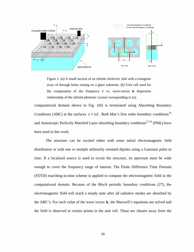
and Anisotropic Perfectly Matched Layer absorbing boundary conditions17,18 (PML) have
been used in this work.
The structure can be excited either with some initial electromagnetic field
distribution or with one or mutiple arbitrarily oriented dipoles using a Gaussian pulse in
time. If a localized source is used to excite the structure, its spectrum must be wide
enough to cover the frequency range of interest. The Finite Difference Time Domain
(FDTD) marching-in-time scheme is applied to compute the electromagnetic field in the
computational domain. Because of the Bloch periodic boundary conditions (27), the
electromagnetic field will reach a steady state after all radiative modes are absorbed by
the ABC’s. For each value of the wave vector k , the Maxwell’s equations are solved and
the field is observed at certain points in the unit cell. These are chosen away from the
Figure 1. (a) A small section of an infinite dielectric slab with a triangular
array of through holes resting on a glass substrate; (b) Unit cell used for
the computation of the frequency ν vs. wave-vector k dispersion
relationship of the infinite photonic crystal corresponding to (a).
17
symmetry planes of the lattice, (unless some particular symmetry class of the modes is
under consideration,) to avoid the possibility of probing the field in the node of a mode.
The Fourier Transform of the computed signal has peaks at frequencies of the vertically
confined modes that can propagate in the structure with the given wave vector k . The
computational time must be long enough to allow the desired frequency resolution.
We have computed the dispersion diagram ν versus k, of a perforated dielectric
slab (ε=12) sitting on a glass substrates (ε=2.25) sketched in Fig. 1(a) using this
technique. Wave propagation in a similar freestanding structure was previously
calculated using the plane wave expansion method with the super-cell approach19.
ΓΓ0
0.1
0.2
0.3
0.4
0.5
0.6F
requ
ency
in u
nits
of (
c/a)
M K
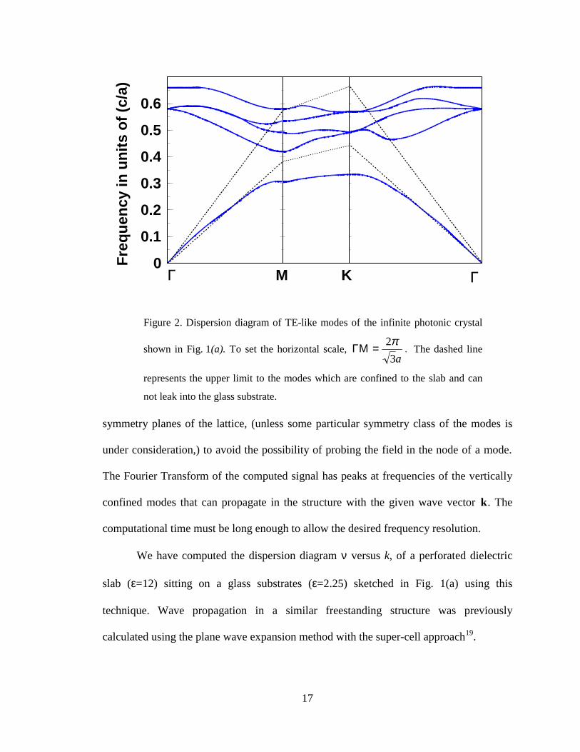
Figure 2. Dispersion diagram of TE-like modes of the infinite photonic crystal
shown in Fig. 1(a). To set the horizontal scale, a3
2π=ΓΜ . The dashed line
represents the upper limit to the modes which are confined to the slab and can
not leak into the glass substrate.
18
Figure 2 shows the dispersion diagram for the TE-like guided modes of the structure
when the propagation vector k lies in the x-y plane. The ratio between the thickness t of
the slab and the lattice constant a was chosen to be t/a = 0.333, while the radius r of the
holes was chosen to be r = 0.40a. These parameters seem to give the smallest possible
mode volume. A wide forbidden gap for the TE-like modes exists in the range of
normalized frequencies 0.33c/a≤ν≤0.43c/a. As will be shown below, this 2-dimensional
photonic band-structure can be used as a reflecting medium to create a cavity with a very
small mode volume.
Another important feature of the band structure is that all upper bands are
relatively flat. We can say that modes with different values of the wave vector are have
limited disperison. As will be discussed in the Chapter 5, this leads to the angle-
integrated resonant enhancement of the emission into the leaky modes.
3.2. Numerical Results: Investigation of candidate nano-cavities
Introduction of an irregularity in the periodic structure of a photonic crystal, often
referred to as a defect, may cause localization of one or more electromagnetic modes
around the defect itself. To completely characterize these localized resonant modes, we
have considered a finite sized photonic crystal with a defect close to its center, and we
have employed the FDTD using absorbing boundary conditions on all boundaries of the
computational domain.
The Fourier Transform of the electromagnetic field at observation points inside the
cavity gives the resonant frequencies of the cavity, while the Q of each mode can be
19
estimated from the decay rate of the energy stored in the cavity. It must be noted that the
numerical computation of the cavity Q is very sensitive to several parameters. In
particular, to the value of the dielectric material, the kind of absorbing boundary
conditions used to terminate the computational domain, and to the distance between the
open dielectric cavity and the boundary of the computational domain.
As was mentioned before, to achieve high enhancement of spontaneous emission
rate the resonant mode of a cavity must have the smallest possible volume while its Q
must be larger than Qm=νm/∆νm of the active material20, where νm and ∆νm are the
frequency and linewidth of the material transition. A Figure-of-Merit for the cavity
optimization is the mode’s effective volume normalized to the cubic half wavelength of
the resonant mode (λ/2n)3 in the medium of refractive index n:
( )max23
32
3 )()()2/(
)()(
)2/( rEr
rrEr
ελ
ε
λ n
d
n
Veff ∫= (28)
The FDTD algorithm allows the computation of the effective volume either in the time
domain or in the frequency domain by post-processing the computed data. Particular care
must be exercised to deal with some numerical issues when computing the effective
mode volume. The integration in equation (28) must be performed over a volume
enclosing the geometrical defect and large enough to enclose also the mode’s
electromagnetic energy that spills outside the slab. Also, the search for the maximum
value of the electric energy must be carried out in the same volume and preferably along
the symmetry planes of the structure. This is to avoid the numerical artifact of high
20
electric field at certain dielectric interfaces
due to the discretization of geometry
necessary for the Finite Difference
computation.
When these considerations are kept
in mind, the FDTD technique is a flexible
tool to calculate resonant frequencies, field
and energy distribution of resonant modes,
as well as their Q and effective volume.
All this information is necessary for a
proper design of efficient cavity-enhanced
light-emitting diodes.
3.3. Analyzed structures
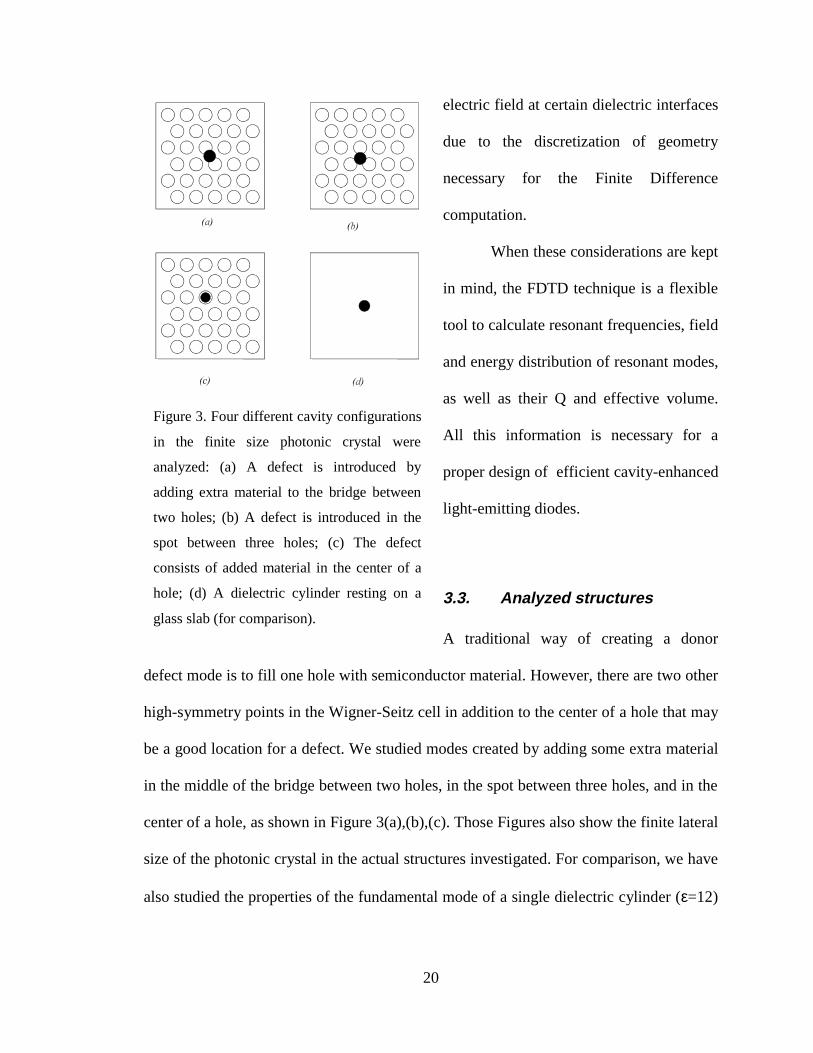
A traditional way of creating a donor
defect mode is to fill one hole with semiconductor material. However, there are two other
high-symmetry points in the Wigner-Seitz cell in addition to the center of a hole that may
be a good location for a defect. We studied modes created by adding some extra material
in the middle of the bridge between two holes, in the spot between three holes, and in the
center of a hole, as shown in Figure 3(a),(b),(c). Those Figures also show the finite lateral
size of the photonic crystal in the actual structures investigated. For comparison, we have
also studied the properties of the fundamental mode of a single dielectric cylinder (ε=12)
Figure 3. Four different cavity configurations
in the finite size photonic crystal were
analyzed: (a) A defect is introduced by
adding extra material to the bridge between
two holes; (b) A defect is introduced in the
spot between three holes; (c) The defect
consists of added material in the center of a
hole; (d) A dielectric cylinder resting on a
glass slab (for comparison).
21
located on the same glass substrate (ε=2.25) supporting the 2-D photonic crystal (Figure
3d). These structures can be described by three independent dimensionless parameters:
normalized thickness t/a, normalized radius of the holes r/a and normalized radius of the
0 0.2 0.4 0.6 0.8 1
Defect Volume / Hole Volume
0102030405060708090
100
Cav
ity Q
012345678
Mod
e E
ffect
ive
Vol
ume
i
n un
its o
f (λ
/2n)
3
0.3
0.33
0.36
0.39
0.42
0.45
0.48
Res
onan
t Fre
quen
cy
in
uni
ts o
f (c/
a)
Conduction Band
Valence Band (a)
(b)
(c)
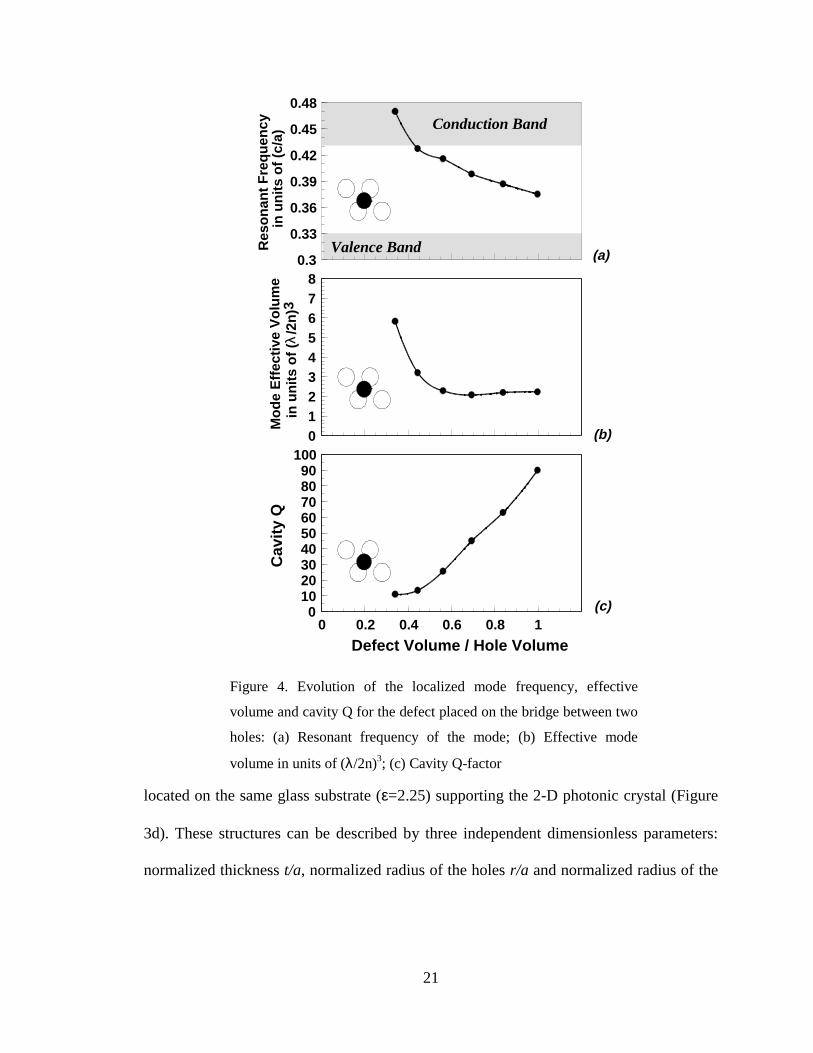
Figure 4. Evolution of the localized mode frequency, effective
volume and cavity Q for the defect placed on the bridge between two
holes: (a) Resonant frequency of the mode; (b) Effective mode
volume in units of (λ/2n)3; (c) Cavity Q-factor
22
defect rd/a. Therefore, optimization of the dimensionless effective volume f has to be
performed in the three-dimensional parameter space.
0 0.2 0.4 0.6 0.8 1
Defect Volume / Hole Volume
0102030405060708090
100
Cav
ity Q
012345678
Mod
e E
ffect
ive
Vol
ume
in
uni
ts o
f (λ
/2n)
30.3
0.33
0.36
0.39
0.42
0.45
0.48
Res
onan
t Fre
quen
cy
in
uni
ts o
f (c/
a)
Conduction Band
Valence Band(a)
(b)
(c)
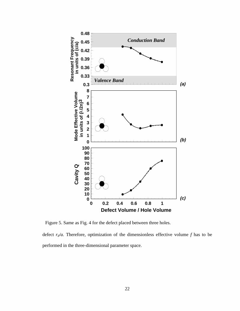
Figure 5. Same as Fig. 4 for the defect placed between three holes.
23
3.4. Cavity Characteristics
Relative thickness, t/a, of the structure did not influence the mode volume results
much. For all the studied geometries, the best effective volume was achieved at t/a~1/3.
For technological reasons, the walls between holes should not be too thin. We have
chosen r/a=0.4, even though larger values of r/a may produce slightly better results.
Figures 4, 5 and 6 show the variation of frequency, the normalized effective volume, and
the Q of the lowest order resonant modes versus the defect size for the different cavity
geometries. Typically for all donor modes, the frequency of the mode emerges from the
conduction band-edge at 0.43c/a and decreases towards the frequency of 0.33c/a of the
valence band. As can be seen from these Figures, the resonant frequencies of all
structures with the same defect size are roughly the same. This suggests an alternative
viewpoint: The defect mode is the mode of a single cylindrical resonator “tuned” to the
forbidden gap of the photonic crystal, to provide additional mode confinement and higher
Q. For small defect size, quality factors are normally on the order of 10. As the mode
volume reaches its minimum, Q goes up to 40 or even up 90 as in the case of the bridge
defects. It is typical for all modes to have cavity Q increasing as mode volume goes
down. Indeed, the more tightly localized the mode, the smaller its tails outside of a finite
sized photonic crystal. By comparison, the cavity Q of an isolated cylinder21 is
0.016×n3≈7 and mode volume is 4.52(λ/2n)3, under our conditions. Probably the most
interesting feature is that the minimum of the effective volumes is about Veff≈2(λ/2n)3 for
all three defect types. This make us wonder if there is a fundamental lower limit on the
volume size achievable with a certain dielectric material! We believe the mode volume
24
results for 3-d photonic crystal structures with full 3-d confinement would actually be
quite similar, since index guiding provides commensurate vertical confinement. In
addition, the case of 1-d periodicity with index guiding in the other two dimensions leads
to a volume only 25% higher than 2(λ/2n)3. Computation of the flux of the Poynting
0 0.2 0.4 0.6 0.8 1
Defect Volume / Hole Volume
0102030405060708090
100
Cav
ity Q
012345678
Mod
e E
ffect
ive
Vol
ume
in
uni
ts o
f (λ
/2n)
30.3
0.33
0.36
0.39
0.42
0.45
0.48
Res
onan
t Fre
quen
cy
in u
nits
of (
c/a)
Conduction Band
Valence Band (a)
(b)
(c)
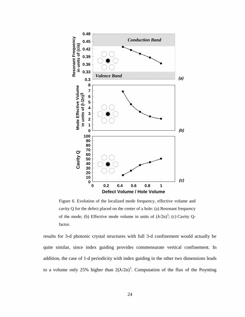
Figure 6. Evolution of the localized mode frequency, effective volume and
cavity Q for the defect placed on the center of a hole: (a) Resonant frequency
of the mode; (b) Effective mode volume in units of (λ/2n)3; (c) Cavity Q-
factor.
25
vector through a surface enclosing the slab reveals that most of the energy of the defect
mode leaks in the vertical direction, rather than being guided by the slab. Therefore
increasing the lateral size of the crystal is not likely to increase the cavity Q by much.
(a)(b)
(c) (d)
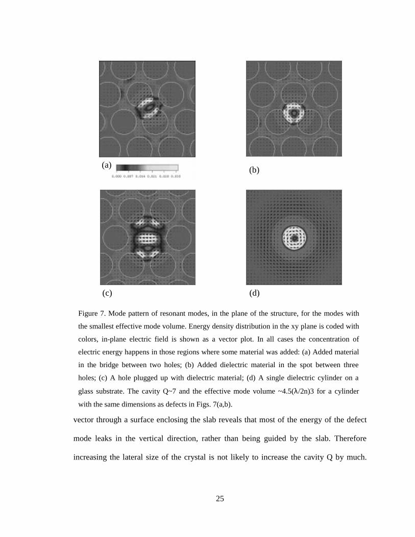
Figure 7. Mode pattern of resonant modes, in the plane of the structure, for the modes with
the smallest effective mode volume. Energy density distribution in the xy plane is coded with
colors, in-plane electric field is shown as a vector plot. In all cases the concentration of
electric energy happens in those regions where some material was added: (a) Added material
in the bridge between two holes; (b) Added dielectric material in the spot between three
holes; (c) A hole plugged up with dielectric material; (d) A single dielectric cylinder on a
glass substrate. The cavity Q~7 and the effective mode volume ~4.5(λ/2n)3 for a cylinder
with the same dimensions as defects in Figs. 7(a,b).
26
The limited required size is a valuable feature in view of possible applications of this type
of resonant cavity in light emitting diode, where many such cavities might need to be
crowded together.
Figure 7 shows the electric field and energy density distribution of the modes with
the smallest effective volumes for all studied configurations, along a z=const plane in the
middle of the slab. The electric energy density reaches its maximum almost in the center
of the dielectric slab. Electric energy density is coded with colors in Fig. 7, and the
corresponding projection of the electric field onto the horizontal plane is shown as a
vector plot. All these modes are predominantly TE, that is electric field mostly oscillates
in the xy plane. Due to different locations of the defect, these modes have different
symmetries. Structures with a defect introduced into the bridge between two and tree
holes, have C2v and C3v symmetry respectively, and their resonant modes are not
degenerate. These modes bear close resemblance with the “donut” mode TE01δ of a
cylindrical cavity, shown in Figure 7d.
Considering the case of a defect created by adding material to the center of a hole,
the smallest effective mode volume is surprisingly achieved for rd/a=0.4, that is when the
hole is completely plugged. The electric energy distribution of the resonant mode (Figure
7c) has a maximum in the center, which makes the mode a prospective candidate for use
in resonant-cavity LED applications, where the active material is placed in the center of
the filled hole. Moreover, since this structure has C6v symmetry, the resonant mode is
doubly degenerate. According to Equation (25), this fact implies g=2 into the formula of
the enhancement factor. For example, in the semiconductor light emitter In0.53Ga0.47As,
27
with Qm=10 at room temperature, plugging Veff=2(λ/2n)3 into Equation (25) gives a five-
fold spontaneous emission enhancement Γ/Γ0=5.
3.5. Summary of numerical results
In this chapter we have described how the band structure of the thin slab photonic
crystal was calculated. It was shown that the photonic conduction bands of the photonic
crystal are above the light cone and are relatively flat. The defect modes in a dielectric
slab photonic crystal have been numerically optimized with respect to the mode volume
using the Finite Difference Time Domain algorithm. A record low value of only 2(λ/2n)3
is shown to be achievable in either of three different configurations. This small mode
volume can lead to a significant enhancement of spontaneous emission rates in
semiconductor nano-cavities due to the Purcell effect. As will be shown later, a similar
effect can be achieved in a perfectly periodic photonic crystal without defects when the
emission line of the material is tuned to the leaky conduction bands above the photonic
bandgap.
28
4. Surface Recombination Measurements on Candidate Materials
for Nano-cavity Light Emitting Diodes
As the size of opto-electronic devices becomes smaller, surface effects begin to
influence their performance. Surface recombination imposes limitations on the efficiency
of nanocavity light-emitting diodes, VCSEL’s with oxidized apertures, and other devices
which require the size of the active region to be comparable to the diffusion length of
minority carriers. In this study we concentrated on surface characterization of different
material systems, and we identified those suitable for the fabrication of active opto-
electronic devices. This chapter is organized as follows: first we describe the
experimental setup and the absolute calibration technique, then we introduce the
recombination properties we are measuring or modeling. A radiative transport model
based on the photon gas22 approximation is used to extract internal quantum efficiency
from the photoluminescence measurements in the context of an InxGa1-xN sample. The
same model with slight modification was used for two other systems - In0.5(Ga1-xAl x)0.5P
and InxGa1-xAs. Gallium nitride and chemically passivated InGaAs will be shown to
possess a relatively low surface recombination velocity (on the order of 104cm/s) while
the InGaAlP material system has surface recombination velocity an order of magnitude
higher. We show also that surface damage produced by chemically-assisted ion beam
etching can be cured by a gentle wet etching and chemical passivation.
29
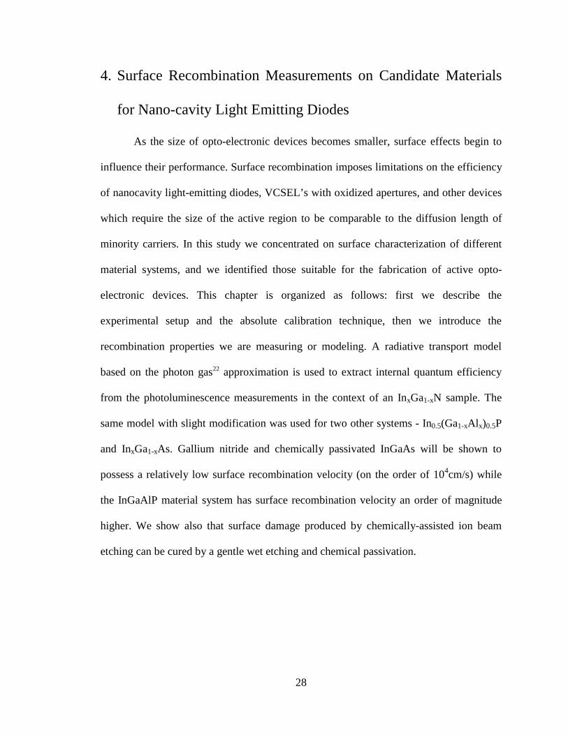
4.1. Experimental setup
Values of surface recombination velocity were determined by absolute
photoluminescence efficiency measuremets, using a setup as shown in Figure 8. Samples
are optically pumped with the appropriate laser photon energy above the bandgap. The
absolute external quantum efficiency is calibrated by referencing the measured
photoluminescence against the scattered light reading from a perfect white Lambertian
reflector25. In this way, the collection cone of the photodetector is identical in both
measurements. Corrections are made for different transmission through the optical setup
and the detector quantum efficiency ratio at the photoluminescence and pump
Figure 8. Experimental setup for photoluminescence measurements. The
absolute external quantum efficiency is measured by calibrating the measured
photoluminescence from the sample against the reading measured from the
laser scattered off a perfect white Lambertian reflector. The collection cone is
the same for both measurements, so that only a correction for the system
wavelength dependence of detector quantum efficiency has to be taken into
account.
30
wavelengths. A radiative transport model is used to obtain the internal quantum
efficiency of the active material from the measured external quantum efficiency.
Furthermore, comparison of the internal quantum efficiency from double heterostructure
samples against that from the samples with an exposed active region provides
information on the surface recombination velocity of exposed surfaces.
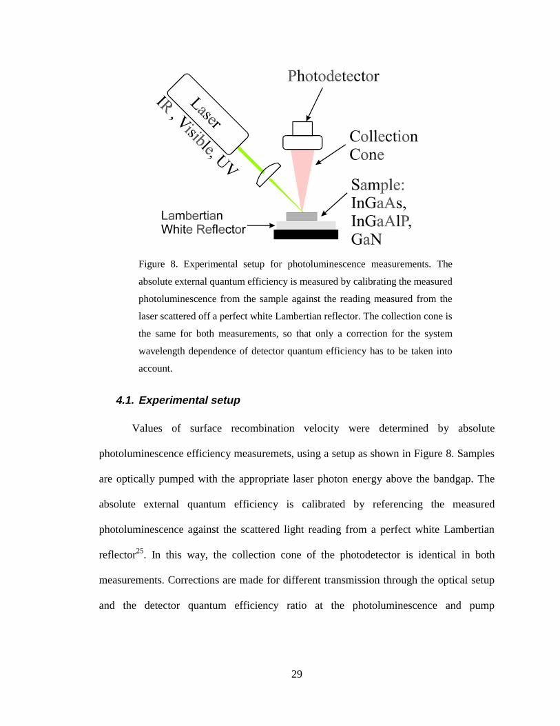
4.2. Radiative transport model
We begin with some definitions:
1) External quantum efficiency ηext is defined as a ratio of the number of PL photons
coming out of the sample to the number of photons absorbed in the sample. This is a
quantity we can measure.
2) Internal quantum efficiency ηint is the probability that an electron-hole pair created in
the active region will recombine radiatively. Internal radiative quantum efficiency is a
Figure-of-merit for an opto-electronic material.
3) Light extraction efficiency ηextraction is the fraction of internally generated PL photons
that manage to escape from the sample. It depends strongly on the geometry of the
sample. It also depends on the internal quantum efficiency if reabsorption in the active
region has to be taken into account. For certain simple geometries, light extraction
efficiency can be easily calculated.
4) Finally, if optical pumping creates electron-hole pairs outside of the active region, we
define collection efficiency ηcoll as a fraction of carriers that diffuse to the active region.
31
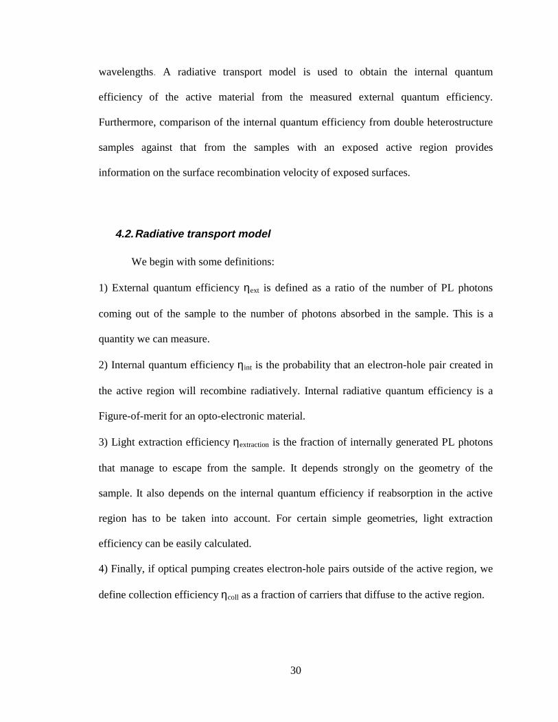
If all carriers are collected in the active region ηcoll =1.
Combining all these definitions, external quantum efficiency can be expressed in terms of
three other quantities, which can be measured or calculated:
extractcollexternal ηηηη int= (29)
Initially we will describe radiative transport model used to calculate internal
quantum efficiency in GaN. (For InGaAlP and InGaAs the models employed are almost
identical, except they take into account sample’s structure such as an absorbing substrate
in the case of InGaAlP.) As can be seen from the Figure 9a, the InGaN model considers a
film of (refractive index nGaN=2.3) grown on the sapphire substrate with refractive index
nS=1.8 . There are two critical angles and two escape cones associated with them: total
2θc2
2θc1
Sapphiren=1.8
InGaNn=2.3
Air, n=1
White reflector or black wax
MQW region
Figure 9a. The semicinductor structure corresponding to the radiative
transport model consists of a thin semiconductor film sitting on a sapphire
substrate.
32
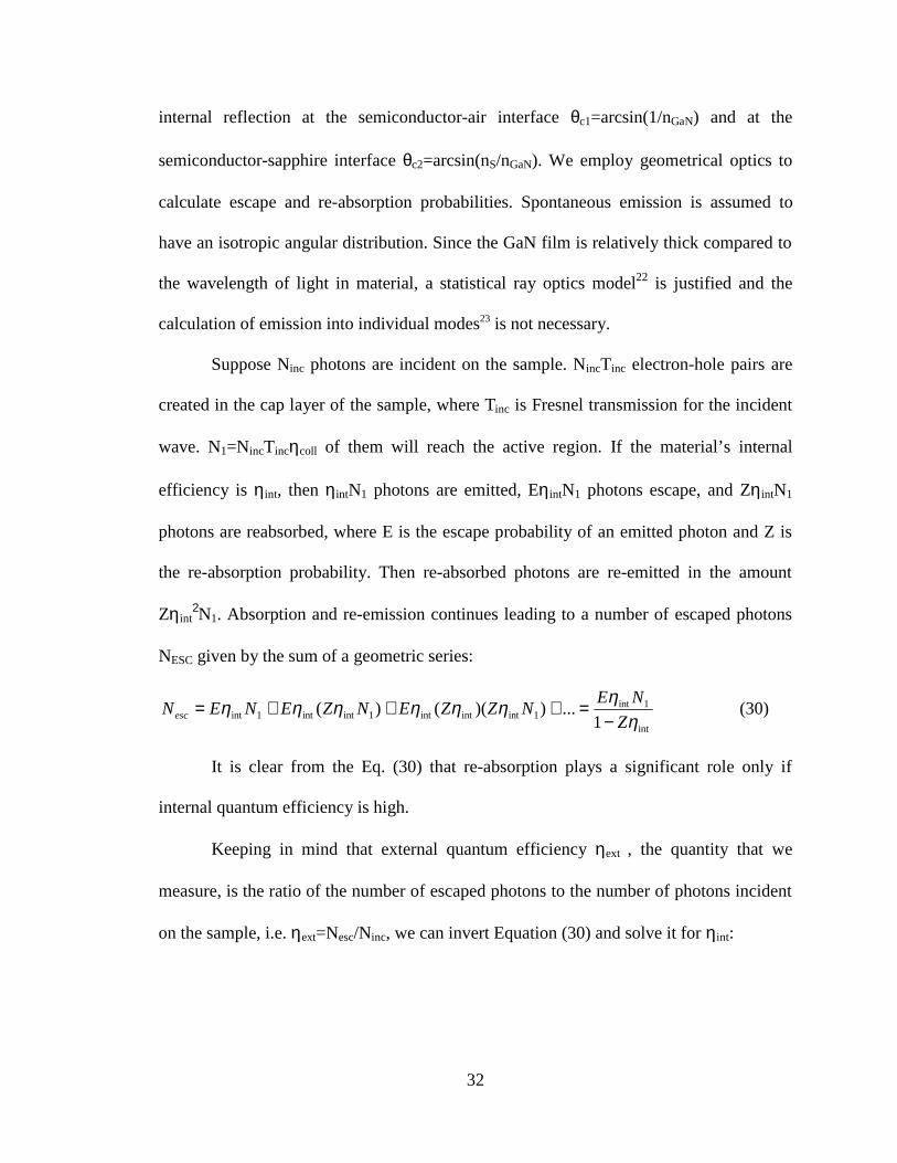
internal reflection at the semiconductor-air interface θc1=arcsin(1/nGaN) and at the
semiconductor-sapphire interface θc2=arcsin(nS/nGaN). We employ geometrical optics to
calculate escape and re-absorption probabilities. Spontaneous emission is assumed to
have an isotropic angular distribution. Since the GaN film is relatively thick compared to
the wavelength of light in material, a statistical ray optics model22 is justified and the
calculation of emission into individual modes23 is not necessary.
Suppose Ninc photons are incident on the sample. NincTinc electron-hole pairs are
created in the cap layer of the sample, where Tinc is Fresnel transmission for the incident
wave. N1=NincTincηcoll of them will reach the active region. If the material’s internal
efficiency is ηint, then ηintN1 photons are emitted, EηintN1 photons escape, and ZηintN1
photons are reabsorbed, where E is the escape probability of an emitted photon and Z is
the re-absorption probability. Then re-absorbed photons are re-emitted in the amount
Zηint2N1. Absorption and re-emission continues leading to a number of escaped photons
NESC given by the sum of a geometric series:
int
1int1intintint1intint1int 1
...))(()(η
ηηηηηηηZ
NENZZENZENENesc −
=+++= (30)
It is clear from the Eq. (30) that re-absorption plays a significant role only if
internal quantum efficiency is high.
Keeping in mind that external quantum efficiency ηext , the quantity that we
measure, is the ratio of the number of escaped photons to the number of photons incident
on the sample, i.e. ηext=Nesc/Ninc, we can invert Equation (30) and solve it for ηint:
33
,)/(
)/(int
incextcoll
incext
ETZ
ET
ηηη
η+
= (31)
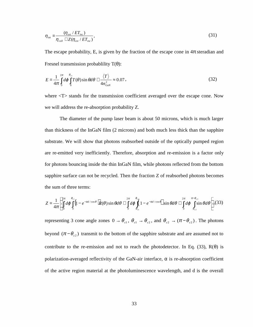
The escape probability, E, is given by the fraction of the escape cone in 4π steradian and
Fresnel transmission probablility T(θ):
07.04
sin)(4
1 2
0 02
1
≈≅= ∫ ∫π θ
θθθϕπ
c
GaNn
TdTdE , (32)
where <T> stands for the transmission coefficient averaged over the escape cone. Now
we will address the re-absorption probability Z.
The diameter of the pump laser beam is about 50 microns, which is much larger
than thickness of the InGaN film (2 microns) and both much less thick than the sapphire
substrate. We will show that photons reabsorbed outside of the optically pumped region
are re-emitted very inefficiently. Therefore, absorption and re-emission is a factor only
for photons bouncing inside the thin InGaN film, while photons reflected from the bottom
sapphire surface can not be recycled. Then the fraction Z of reabsorbed photons becomes
the sum of three terms:
( ) ( )
+−+−= ∫ ∫∫ ∫∫ ∫
−−−
π θπ
θ
π θ
θ
θαπ θ
θα θθϕθθϕθθθϕπ
2
0
2
0
cos/2
0 0
cos/2
2
2
1
1
sinsin1sin)(14
1dddeddRedZ
c
c
c
c
c
dd ,(33)
representing 3 cone angle zones 10 cθ→ , 21 cc θθ → , and )( 22 cc θπθ −→ . The photons
beyond )( 2cθπ − transmit to the bottom of the sapphire substrate and are assumed not to
contribute to the re-emission and not to reach the photodetector. In Eq. (33), R(θ) is
polarization-averaged reflectivity of the GaN-air interface, α is re-absorption coefficient
of the active region material at the photoluminescence wavelength, and d is the overall
34
thickness of the absorbing quantum wells. The first term in Eq. (33) describes to the re-
absorption within the inner escape cone θc1. The second term corresponds to re-
absorption of photons emitted within the second escape cone θc2 but outside of the first.
These photons cross the active region once before they go into the substrate. The third
term refers to re-absorption of totally internally reflected light in the semiconductor film.
This last term dominates re-absorption and is simply Znn GaNs ≈≅− 62.0/1 22 , while the
two other terms are merely corrections. In this analysis we have assumed that light
reflected from the sapphire-air interface is re-absorbed outside of the optically pumped
region and does not contribute efficiently to further photoluminescence.
There is a problem with Eq. (31), since the ηcoll on the right hand side is not exactly
known, but is surely less then 1. Therefore Eq. (31) is merely a lower limit to ηint:
,)/(1
)/(int
incext
incext
ETZ
ET
ηη
η+
≥ (34)
Likewise, Eq. (31) can be solved for the collection efficiency ηcoll:
,)1)(/(
int
int
ηηη
ηZETincext
coll
−= (35)
Once again, ηint on the right hand side of Eq. (35) is not exactly known, but it’s surely
less then 1. Therefore Eq. (35) places a lower limit on carrier collection efficiency:
35
)1)(/( ZETincextcoll −≥ ηη (36)
Thus a measurement of ηext can place a lower limit on ηint through Eq. (34) and a lower
limit on ηcoll through Eq. (36). This procedure will be useful if the experimental results
for ηext point to limits on ηint and ηcoll that are reasonably close to 1. For InGaN for
example, the limits are 0.87<ηint <1 and 0.87<ηcoll<1, constraining the experimental
values very tightly.
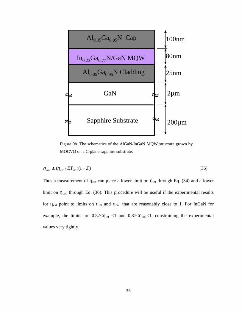
Al 0.05Ga0.95N Cap
In0.23Ga0.77N/GaN MQW
GaN
Sapphire Substrate
Al0.05Ga0.95N Cladding
100nm
80nm
25nm
2µm
200µm
Figure 9b. The schematics of the AlGaN/InGaN MQW structure grown by
MOCVD on a C-plane sapphire substrate.
36
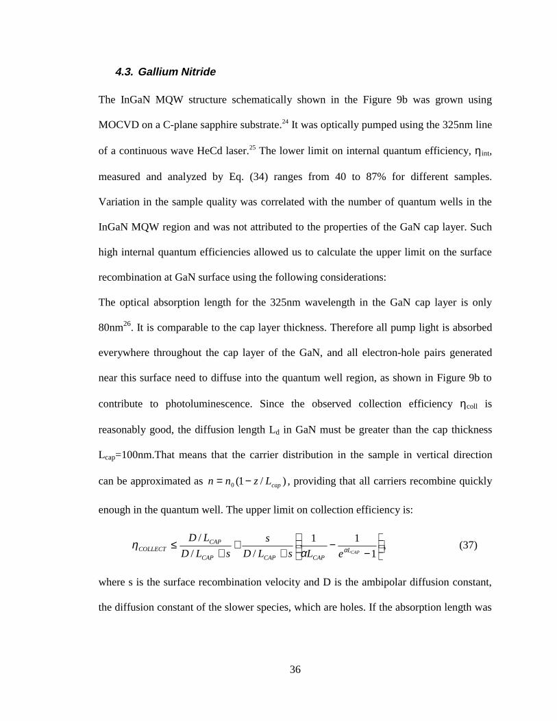
4.3. Gallium Nitride
The InGaN MQW structure schematically shown in the Figure 9b was grown using
MOCVD on a C-plane sapphire substrate.24 It was optically pumped using the 325nm line
of a continuous wave HeCd laser.25 The lower limit on internal quantum efficiency, ηint,
measured and analyzed by Eq. (34) ranges from 40 to 87% for different samples.
Variation in the sample quality was correlated with the number of quantum wells in the
InGaN MQW region and was not attributed to the properties of the GaN cap layer. Such
high internal quantum efficiencies allowed us to calculate the upper limit on the surface
recombination at GaN surface using the following considerations:
The optical absorption length for the 325nm wavelength in the GaN cap layer is only
80nm26. It is comparable to the cap layer thickness. Therefore all pump light is absorbed
everywhere throughout the cap layer of the GaN, and all electron-hole pairs generated
near this surface need to diffuse into the quantum well region, as shown in Figure 9b to
contribute to photoluminescence. Since the observed collection efficiency ηcoll is
reasonably good, the diffusion length Ld in GaN must be greater than the cap thickness
Lcap=100nm.That means that the carrier distribution in the sample in vertical direction
can be approximated as )/1(0 capLznn −= , providing that all carriers recombine quickly
enough in the quantum well. The upper limit on collection efficiency is:
−
−+
++
≤1
11
//
/CAPL
CAPCAPCAP
CAPCOLLECT
eLsLD
s
sLD
LDαα
η , (37)
where s is the surface recombination velocity and D is the ambipolar diffusion constant,
the diffusion constant of the slower species, which are holes. If the absorption length was
37
smaller than the cap thickness, that is αLcapI1 this equation would reduce to a simpler
expression corresponding to having all carriers generated at the surface:
sLD
LD
CAP
CAPCOLLECT +
≤/
/η
Combining Eqs. (33) and (37) yields an upper limit on the surface recombination velocity
in GaN to be S<0.28D/L~28000 cm/s with diffusion constant assumed27 to be 1 cm2/s in
undoped InGaN.
The optical model described above neglects reflections from the bottom surface of the
sapphire substrate since most of those photons are reflected and absorbed outside of the
optically pumped region, and can not be re-emitted. To verify this assumption we
compared photoluminescence from a sample with the bottom surface and edges coated
with the absorbing black wax to that of the same sample sitting on the white reflecting
surface. As expected, results of these measurements did not differ.
The pump level for these experiments was 10mW onto a 25µm diameter spot, or
~1000A/cm2. At lower pumping intensities the internal photoluminescence goes down,
explaining why absorption and emission outside of the pumped region is so inefficient
and can be neglected.
Fabrication of the miniature devices often involves dry etching. To see the effect of the
dry etching on the surface recombination velocity we exposed the top surface of the one
of the best samples to chemically assisted ion beam etching (Ar+ + Cl2). After etching
about 10 nanometers of the cap layer away, the measured quantum efficiency dropped by
a factor of 5, which corresponds to the surface recombination velocity s=105cm/s on the
38
damaged surface. However, subsequent short wet etch cleaning in the hot KOH which
removed another 5-10nm of the AlGaN cap brought the sample’s efficiency back to about
80% of the initial efficiency. That indicates that ion damage in nitride materials
introduced by the dry etching can be effectively removed.
4.4. InGaAlP
In this case we studied samples consisting of 0.75µm thick In0.5(Ga1-xAl x)0.5P (λ=615nm,
λ=630nm) active region doped at n=1017cm-3 level sandwiched between n-type InAlP
cladding layers grown on an absorbing GaAs substrate (Figure 10a). The sample was
optically pumped with the CW 568nm argon-krypton laser which is not absorbed by the
InAlP cladding layer. The iso-type double hetero-structure allowed us to be un-concerned
about effects related to a p-n junction. Internal quantum efficiency of the as-grown
double hetero-structure sample was measured to be 80%. After the top cladding was
removed with the H3PO4:H2O2:H2O(5:1:1), as shown in Fig. 10b, the surface of the active
region was exposed to air. The PL signal, and hence internal quantum efficiency, dropped
by a factor of 30. Since thickness of the active region is less than the typical diffusion
length in this material system, and there is a potential barrier at the bottom of the active
layer, the carrier density distribution is constant, even though electron-hole generation
occurs mostly at the top interface (see Appendix). For that reason internal quantum
efficiency or an as-grown structure and a structure with an exposed active region is
simply determined by competition between the rates of radiative and non-radiative
recombination. The efficiency of intact double hetero-structure is:
39
RNR
RGROWNAS ττ
τη/1/1
/1
+=− (38)
The efficiency when the InAlP cap of the double hetero-structure is etched away is:
LsRNR
RETCHED //1/1
/1
++=
τττη , (39)
where τR and τNR are radiative and non-radiative minority carrier lifetimes and L is the
thickness of the active region. We can estimate the surface recombination velocity from
the doping level of the active region ND=1017cm-3 and a typical value of the radiative
recombination constant28 B~4⋅10-10 cm3/s using the Equation (38). The recombination
rates would be 1/τR=BND=4⋅107s-1, 1/ τNR=107 s-1. Surface recombination velocity is
easily obtained from (39) and equals to s=105cm/s. This is about twice the surface
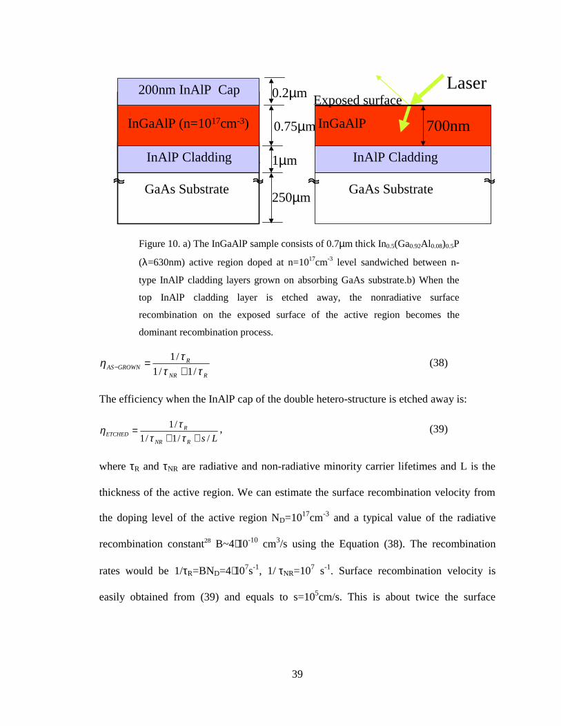
Laser
700nm
Exposed surface200nm InAlP Cap
InAlP Cladding
InGaAlP
GaAs Substrate
InAlP Cladding
InGaAlP (n=1017cm-3)
GaAs Substrate
0.2µm
0.75µm
1µm
250µm
Figure 10. a) The InGaAlP sample consists of 0.7µm thick In0.5(Ga0.92Al 0.08)0.5P
(λ=630nm) active region doped at n=1017cm-3 level sandwiched between n-
type InAlP cladding layers grown on absorbing GaAs substrate.b) When the
top InAlP cladding layer is etched away, the nonradiative surface
recombination on the exposed surface of the active region becomes the
dominant recombination process.
40
recombination velocity previously reported for InGaP29. Surface treatment with
ammonium sulfide used in Ref. 29 did not show any increase in PL signal. The poor
surface properties could be attributed to the presence of aluminum and its oxidation.
Measured surface recombination velocity, although significantly higher than in GaN, is
still an order of magnitude lower than that of a GaAs surface. Still there is a chance that
some chemical treatment or re-growth technique might be established for the InGaAlP
material system. Increasing the doping level may increase radiative recombination, thus
making spontaneous emission more competitive with non-radiative recombination, as
necessary for fabrication of microcavity LED’s. In our PL measurements on the exposed
active region, the surface degraded over a 30s period for an 8mW laser beam focussed in
a 50µm diameter spot. Every time the laser beam was moved to a new location on the
sample, PL refreshed, and then decayed again. At lower pump power, the surface
degraded more slowly. This observation suggests a possibility of sealing or passivation of
the surface before it gets oxidized.
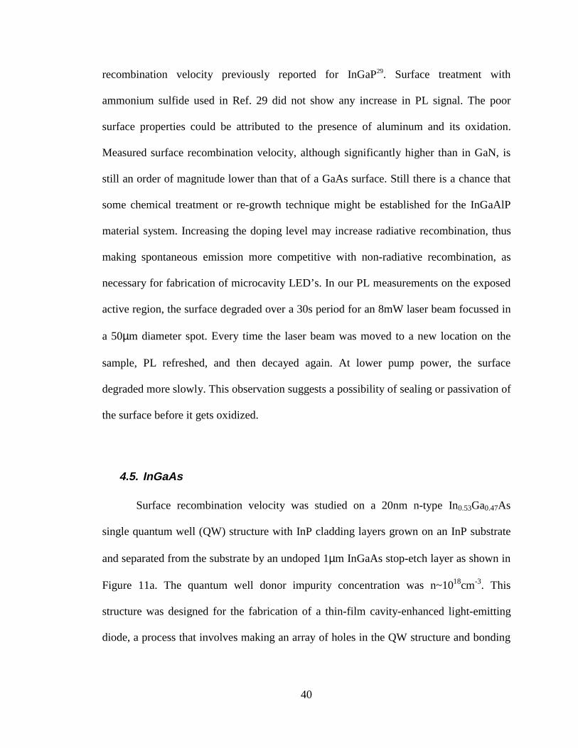
4.5. InGaAs
Surface recombination velocity was studied on a 20nm n-type In0.53Ga0.47As
single quantum well (QW) structure with InP cladding layers grown on an InP substrate
and separated from the substrate by an undoped 1µm InGaAs stop-etch layer as shown in
Figure 11a. The quantum well donor impurity concentration was n~1018cm-3. This
structure was designed for the fabrication of a thin-film cavity-enhanced light-emitting
diode, a process that involves making an array of holes in the QW structure and bonding
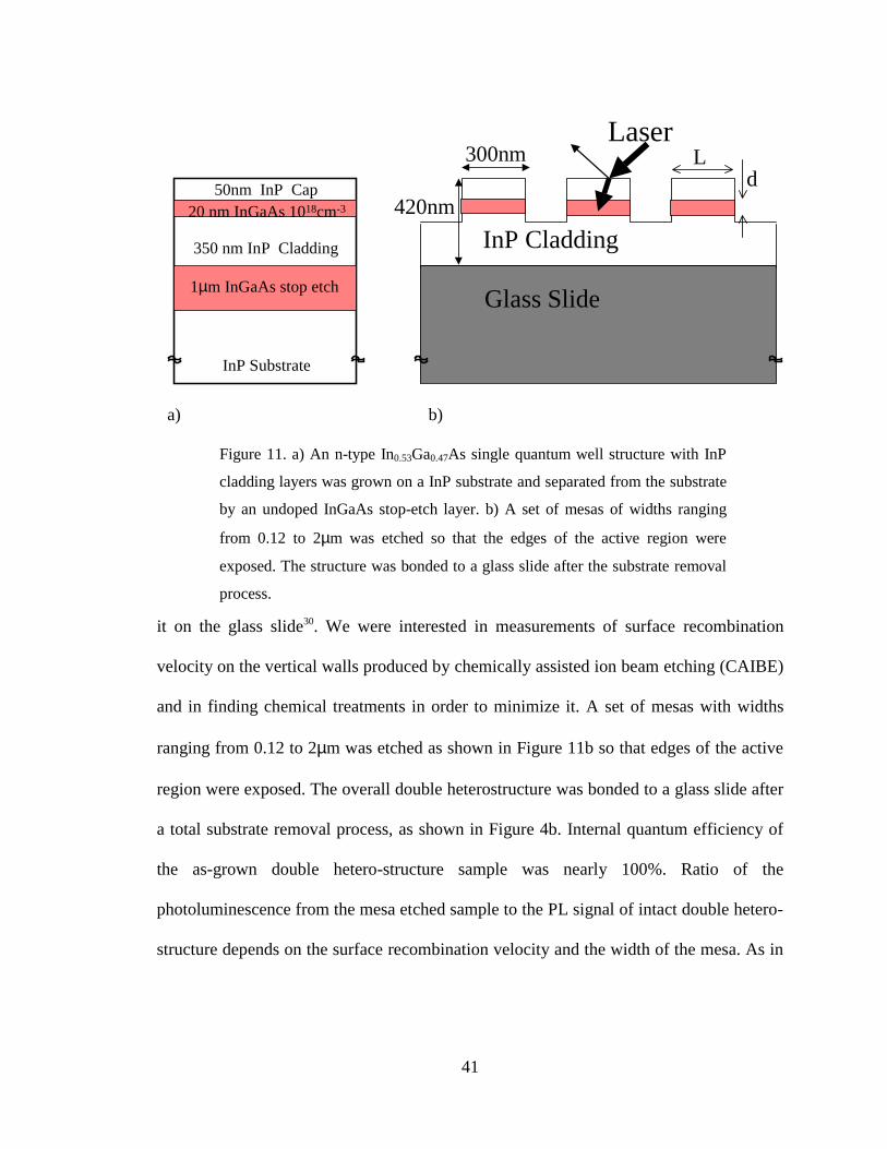
41
it on the glass slide30. We were interested in measurements of surface recombination
velocity on the vertical walls produced by chemically assisted ion beam etching (CAIBE)
and in finding chemical treatments in order to minimize it. A set of mesas with widths
ranging from 0.12 to 2µm was etched as shown in Figure 11b so that edges of the active
region were exposed. The overall double heterostructure was bonded to a glass slide after
a total substrate removal process, as shown in Figure 4b. Internal quantum efficiency of
the as-grown double hetero-structure sample was nearly 100%. Ratio of the
photoluminescence from the mesa etched sample to the PL signal of intact double hetero-
structure depends on the surface recombination velocity and the width of the mesa. As in
350 nm InP Cladding
1µm InGaAs stop etch
InP Substrate
InP Cladding
Laser
20 nm InGaAs 1018cm-3 420nm
Glass Slide
300nm
50nm InP Cap
Ld
a) b)
Figure 11. a) An n-type In0.53Ga0.47As single quantum well structure with InP
cladding layers was grown on a InP substrate and separated from the substrate
by an undoped InGaAs stop-etch layer. b) A set of mesas of widths ranging
from 0.12 to 2µm was etched so that the edges of the active region were
exposed. The structure was bonded to a glass slide after the substrate removal
process.
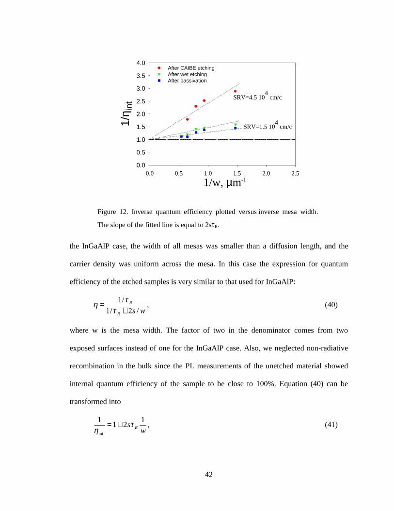
42
the InGaAlP case, the width of all mesas was smaller than a diffusion length, and the
carrier density was uniform across the mesa. In this case the expression for quantum
efficiency of the etched samples is very similar to that used for InGaAlP:
wsR
R
/2/1
/1
+=
ττη , (40)
where w is the mesa width. The factor of two in the denominator comes from two
exposed surfaces instead of one for the InGaAlP case. Also, we neglected non-radiative
recombination in the bulk since the PL measurements of the unetched material showed
internal quantum efficiency of the sample to be close to 100%. Equation (40) can be
transformed into
ws R
121
1
int
τη
+= , (41)
1/w, µm-10.0 0.5 1.0 1.5 2.0 2.5
1/η i
nt
0.0
0.5
1.0
1.5
2.0
2.5
3.0
3.5
4.0After CAIBE etchingAfter wet etchingAfter passivation
SRV=4.5 104 cm/c
SRV=1.5 104 cm/c
Figure 12. Inverse quantum efficiency plotted versus inverse mesa width.
The slope of the fitted line is equal to 2sτR.
43
so that slope of the 1/η vs. 1/w gives value of 2sτR as shown in Figure 12. Fitting data
into the equation is straightforward since the intercept in the Eq. (41) is fixed and equals
to one. The value of the radiative constant “B” was assumed the same as in the InGaAlP
case. We observed surface recombination velocity equal to 4.5⋅104cm/s after the mesas
were etched using CAIBE technique (shown in circles in Fig. 12). After the surface
damage was removed using the gentle wet etch in H2SO4:H2O2:H2O=1:8:5000 solution
(triangles in Fig. 12) SRV decreased to 1.7⋅104cm/s. Further improvement was observed
after the 5 minute long passivation in a solution of ammonium sulfide (NH4)2S (squares,
SRV=1.5⋅104cm/s). It turned out that surface damage depends on the ion energy of the
etching process. The reported results correspond to 500V Ar+ accelerating potential in
CAIBE process. The ion damage seems to be significantly deeper when 1500V voltage is
employed, resulting in larger surface recombination velocities and requiring more
intensive cleaning.
4.6. Summary of material properties
In this chapter we studied surface recombination velocities in InGaN, InGaAlP
and InGaAs material systems using absolute calibration photoluminescence
measurements. Surface recombination velocity is shown to be less than 28000 cm/s in
GaN, 15000cm/s in passivated InGaAs and 105cm/s in InGaAlP. We also showed that
residual surface damage caused by dry etching could be removed by proper surface
44
treatment. These results suggested InGaAs to be the most favorable material system for
nanofabrication of active devices based on photonic crystals.
45
5. Photoluminescence measurements on photonic crystals
5.1. Fabrication of thin film photonic crystals
Two MOCVD-grown In0.47Ga0.53As/InP single quantum well double hetero-structures of
same composition but different thickness were used for these experiments. The samples’
dimensions are shown in the table below.
Structure 1 Structure 2
InP top cladding layer 200nm 90nm
In0.47Ga0.53As, n=1018cm-3 , active region 20nm 60nm
InP bottom cladding layer 200nm 90nm
InGaAs stop etch layer 1000nm 1000nm
InP substrate 300µm 300µm
A standard substrate removal technique was used to fabricate thin films for the
photoluminescence experiments:
The wafer was cleaved in square pieces about 5mm×5mm, and glued to the glass slide
upside down using the UV-curable optical adhesive (Norland 73). The samples were
etched with 70% hydrochloric acid for approximately 2 hours to remove the InP
46
substrate. HCl is a selective etchant for InP with respect to InGaAs. However a special
care should be exercised in order to protect edges of the sample and prevent the etchant
from attacking the InP cladding layer. For this reason it is better to remove the sample
from the solution as soon as the active reaction ceases.
After the InP substrate is removed, the H2SO4:H2O2:H2O (1:8:500) is used to remove the
1µm thick InGaAs stop etch layer. This solution is selective with respect to InP and does
not attack the cladding layer. Its etching rate of InGaAs is approximately 15A per second,
and it takes about 10 minlutes to remove it.
After the substrate removal is complete the sample’s PL is tested using the setup
described in the chapter on surface recombination velocity. Normally the quantum
Figure 13. A triangular array of holes in the thin film on InGaAs/InP double
hetero-structure. The spongy gray substance inside the holes is the optical glue.
Lattice spacing is 720nm, film thickness is 420nm and hole diameter is 550nm.
47
efficiency of the material does not change during the substrate removal procedure and we
end up with a less than half a micron thick, semitransparent film, reliably bonded to the
glass slide. It would be useful to bond the sample to sapphire instead of glass for heat-
sinking considerations, but that would be limited by the thermal conductivity ot the
adhesive in any case.
A set of photonic crystal structures was etched into the thin film samples using
electron-beam lithography and ion beam etching. Normally, each sample had numerous
structures spanning a lattice constant range sufficient for the spontaneous emission band
to overlap with both the photonic bandgap and with conduction band modes. In our case
of emission wavelength centered at λ=1650nm, the photonic crystal’s lattice constant was
made to vary from a=550nm to a=900nm. Correspondingly, the center of the photon band
gap varied from λ=1300nm to λ=1900nm. An SEM picture of a typical structure with
a=720nm, t=420nm and r/a=0.4 is shown in Figure 13.
The etching is performed as follows: A layer of SiO2 is deposited on the sample surface
using plasma chemical vapor deposition. This will be the mask. Next a PMMA resist
(350K molecular weight) for e-beam lithography is spun to a 200nm thickness, and a
desired pattern is written using a Leika EBPG5 e-beam writer running at approximately
5MHz. The pattern is transferred from photoresist to SiO2 mask using directional
chemically assisted ion beam etching (CAIBE) with CHF3 for 6 minute. Finally, the
pattern is transferred into the semiconductor in the same CAIBE machine using CCl4 at
200oC with 200nm/min etch rate. The residual ion damage is cleaned, as discussed in the
chapter 4 by a gentle wet etching in H2SO4:H2O2:H2O (1:8:500) and subsequent surface
48
passivation in a stinking (NH4)2S solution. The effect of passivation on the surface
recombination velocity of InGaAs was discussed in the Chapter 4.
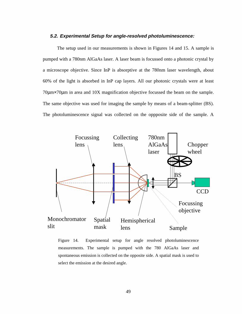
49
5.2. Experimental Setup for angle-resolved photoluminescence:
The setup used in our measurements is shown in Figures 14 and 15. A sample is
pumped with a 780nm AlGaAs laser. A laser beam is focussed onto a photonic crystal by
a microscope objective. Since InP is absorptive at the 780nm laser wavelength, about
60% of the light is absorbed in InP cap layers. All our photonic crystals were at least
70µm×70µm in area and 10X magnification objective focussed the beam on the sample.
The same objective was used for imaging the sample by means of a beam-splitter (BS).
The photoluminescence signal was collected on the oppposite side of the sample. A
780nmAlGaAslaser
CCD
BS
Focussingobjective
SampleHemisphericallens
Collectinglens
Focussinglens
Spatial mask
Monochromatorslit
Chopperwheel
Figure 14. Experimental setup for angle resolved photoluminescence
measurements. The sample is pumped with the 780 AlGaAs laser and
spontaneous emission is collected on the opposite side. A spatial mask is used to
select the emission at the desired angle.
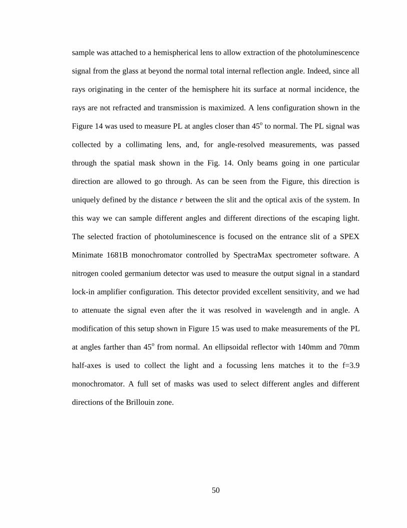
50
sample was attached to a hemispherical lens to allow extraction of the photoluminescence
signal from the glass at beyond the normal total internal reflection angle. Indeed, since all
rays originating in the center of the hemisphere hit its surface at normal incidence, the
rays are not refracted and transmission is maximized. A lens configuration shown in the
Figure 14 was used to measure PL at angles closer than 45o to normal. The PL signal was
collected by a collimating lens, and, for angle-resolved measurements, was passed
through the spatial mask shown in the Fig. 14. Only beams going in one particular
direction are allowed to go through. As can be seen from the Figure, this direction is
uniquely defined by the distance r between the slit and the optical axis of the system. In
this way we can sample different angles and different directions of the escaping light.
The selected fraction of photoluminescence is focused on the entrance slit of a SPEX
Minimate 1681B monochromator controlled by SpectraMax spectrometer software. A
nitrogen cooled germanium detector was used to measure the output signal in a standard
lock-in amplifier configuration. This detector provided excellent sensitivity, and we had
to attenuate the signal even after the it was resolved in wavelength and in angle. A
modification of this setup shown in Figure 15 was used to make measurements of the PL
at angles farther than 45o from normal. An ellipsoidal reflector with 140mm and 70mm
half-axes is used to collect the light and a focussing lens matches it to the f=3.9
monochromator. A full set of masks was used to select different angles and different
directions of the Brillouin zone.
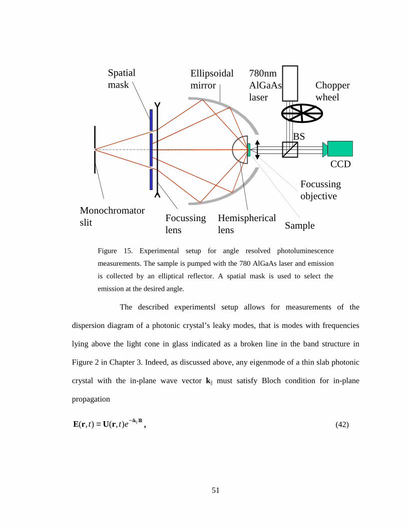
51
The described experimentsl setup allows for measurements of the
dispersion diagram of a photonic crystal’s leaky modes, that is modes with frequencies
lying above the light cone in glass indicated as a broken line in the band structure in
Figure 2 in Chapter 3. Indeed, as discussed above, any eigenmode of a thin slab photonic
crystal with the in-plane wave vector k || must satisfy Bloch condition for in-plane
propagation
RkrUrE ⋅−= ||),(),( iett , (42)
Chopperwheel
CCD
BS
Focussingobjective
Sample
Ellipsoidalmirror
Focussinglens
Spatial mask
Monochromatorslit
780nmAlGaAslaser
Hemisphericallens
Figure 15. Experimental setup for angle resolved photoluminescence
measurements. The sample is pumped with the 780 AlGaAs laser and emission
is collected by an elliptical reflector. A spatial mask is used to select the
emission at the desired angle.
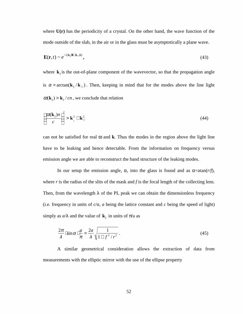
52
where U(r) has the periodicity of a crystal. On the other hand, the wave function of the
mode outside of the slab, in the air or in the glass must be asymptotically a plane wave.
)( ||~),( rkRkrE ⋅+⋅− ⊥iet , (43)
where ||k is the out-of-plane component of the wavevector, so that the propagation angle
is )/arctan( || ⊥= kkα . Then, keeping in mind that for the modes above the line light
cn/)( |||| kk >ω , we conclude that relation
22
2
||
||
)(⊥+>
kk
k
c
nω(44)
can not be satisfied for real ω and k. Thus the modes in the region above the light line
have to be leaking and hence detectable. From the information on frequency versus
emission angle we are able to reconstruct the band structure of the leaking modes.
In our setup the emission angle, α, into the glass is found and as α=atan(r/f),
where r is the radius of the slits of the mask and f is the focal length of the collecting lens.
Then, from the wavelength λ of the PL peak we can obtain the dimensionless frequency
(i.e. frequency in units of c/a, a being the lattice constant and c being the speed of light)
simply as a/λ and the value of ||k in units of π/a as
22 /1
12sin
2rf
aa
+=⋅⋅
λπα
λπ
. (45)
A similar geometrical consideration allows the extraction of data from
measurements with the elliptic mirror with the use of the ellipse property
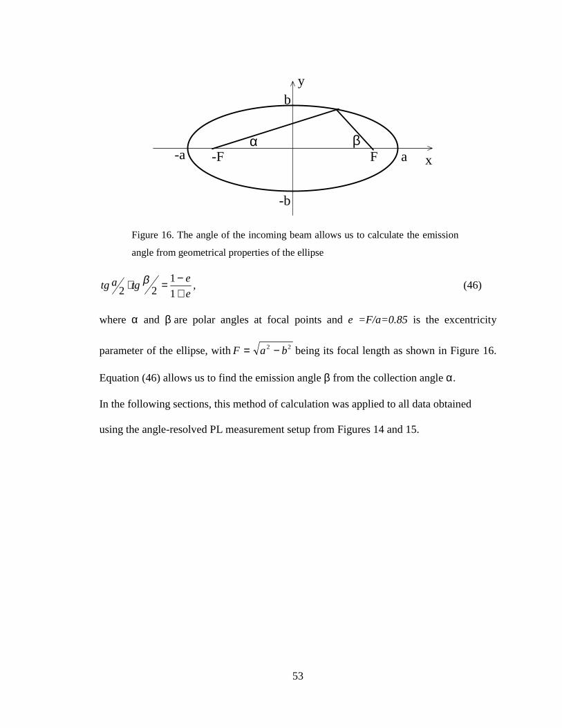
53
e
etgatg
+−=⋅
1
122
β , (46)
where α and β are polar angles at focal points and e =F/a=0.85 is the excentricity
parameter of the ellipse, with 22 baF −= being its focal length as shown in Figure 16.
Equation (46) allows us to find the emission angle β from the collection angle α.
In the following sections, this method of calculation was applied to all data obtained
using the angle-resolved PL measurement setup from Figures 14 and 15.
x
y
F a-a
b
-b
-Fα β
Figure 16. The angle of the incoming beam allows us to calculate the emission
angle from geometrical properties of the ellipse
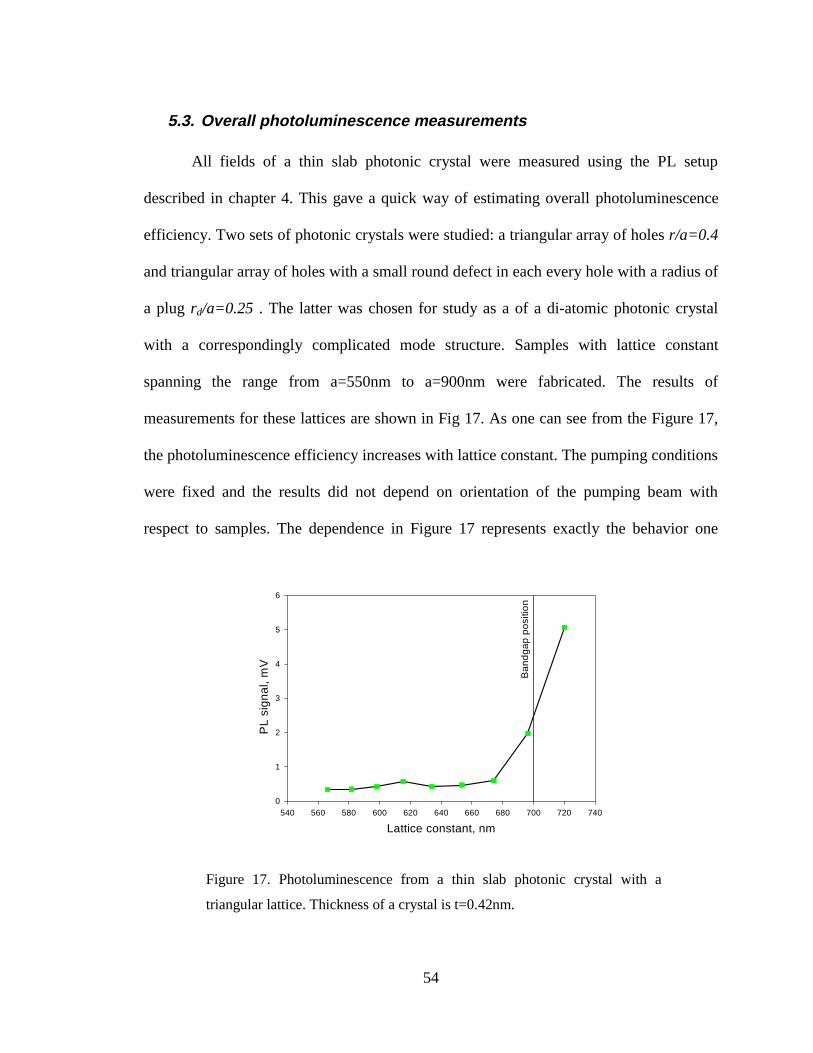
54
5.3. Overall photoluminescence measurements
All fields of a thin slab photonic crystal were measured using the PL setup
described in chapter 4. This gave a quick way of estimating overall photoluminescence
efficiency. Two sets of photonic crystals were studied: a triangular array of holes r/a=0.4
and triangular array of holes with a small round defect in each every hole with a radius of
a plug rd/a=0.25 . The latter was chosen for study as a of a di-atomic photonic crystal
with a correspondingly complicated mode structure. Samples with lattice constant
spanning the range from a=550nm to a=900nm were fabricated. The results of
measurements for these lattices are shown in Fig 17. As one can see from the Figure 17,
the photoluminescence efficiency increases with lattice constant. The pumping conditions
were fixed and the results did not depend on orientation of the pumping beam with
respect to samples. The dependence in Figure 17 represents exactly the behavior one
Lattice constant, nm540 560 580 600 620 640 660 680 700 720 740
PL
sign
al, m
V
0
1
2
3
4
5
6
Ba
ndga
p p
ositi
on
Figure 17. Photoluminescence from a thin slab photonic crystal with a
triangular lattice. Thickness of a crystal is t=0.42nm.
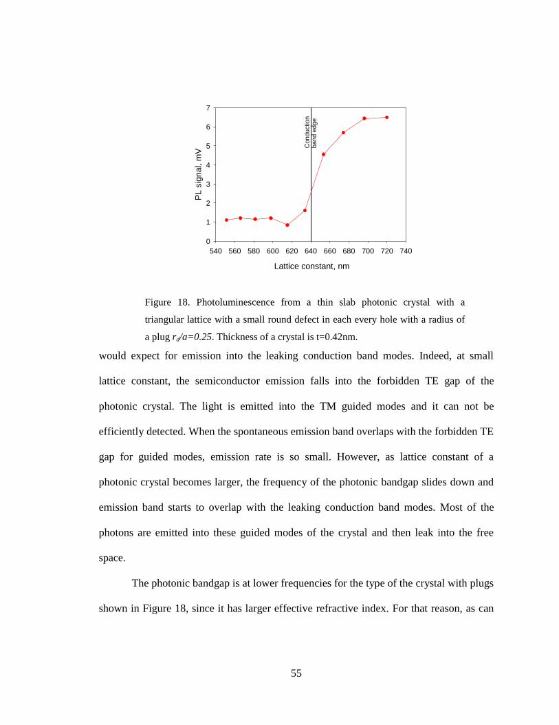
55
would expect for emission into the leaking conduction band modes. Indeed, at small
lattice constant, the semiconductor emission falls into the forbidden TE gap of the
photonic crystal. The light is emitted into the TM guided modes and it can not be
efficiently detected. When the spontaneous emission band overlaps with the forbidden TE
gap for guided modes, emission rate is so small. However, as lattice constant of a
photonic crystal becomes larger, the frequency of the photonic bandgap slides down and
emission band starts to overlap with the leaking conduction band modes. Most of the
photons are emitted into these guided modes of the crystal and then leak into the free
space.
The photonic bandgap is at lower frequencies for the type of the crystal with plugs
shown in Figure 18, since it has larger effective refractive index. For that reason, as can
Lattice constant, nm
540 560 580 600 620 640 660 680 700 720 740
PL
sign
al, m
V
0
1
2
3
4
5
6
7
Con
duct
ion
band
edg
e
Figure 18. Photoluminescence from a thin slab photonic crystal with a
triangular lattice with a small round defect in each every hole with a radius of
a plug rd/a=0.25. Thickness of a crystal is t=0.42nm.
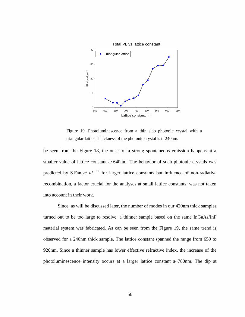
56
be seen from the Figure 18, the onset of a strong spontaneous emission happens at a
smaller value of lattice constant a~640nm. The behavior of such photonic crystals was
predicted by S.Fan et al. 19 for larger lattice constants but influence of non-radiative
recombination, a factor crucial for the analyses at small lattice constants, was not taken
into account in their work.
Since, as will be discussed later, the number of modes in our 420nm thick samples
turned out to be too large to resolve, a thinner sample based on the same InGaAs/InP
material system was fabricated. As can be seen from the Figure 19, the same trend is
observed for a 240nm thick sample. The lattice constant spanned the range from 650 to
920nm. Since a thinner sample has lower effective refractive index, the increase of the
photoluminescence intensity occurs at a larger lattice constant a~780nm. The dip at
Total PL vs lattice constant
Lattice constant, nm
550 600 650 700 750 800 850 900 950
Pl s
igna
l, m
V
0
10
20
30
40
triangular lattice
Figure 19. Photoluminescence from a thin slab photonic crystal with a
triangular lattice. Thickness of the photonic crystal is t=240nm.

57
a=670nm is most probably a fabrication defect. It’s worth noting however that the slight
increase in the PL efficiency at smallest lattice constants is repeatable. We attribute it to
external scattering of the guided modes at the interface between the photonic crystal and
the surrounding unetched area of the experimental film.
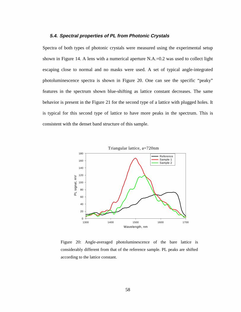
58
5.4. Spectral properties of PL from Photonic Crystals
Spectra of both types of photonic crystals were measured using the experimental setup
shown in Figure 14. A lens with a numerical aperture N.A.=0.2 was used to collect light
escaping close to normal and no masks were used. A set of typical angle-integrated
photoluminescence spectra is shown in Figure 20. One can see the specific “peaky”
features in the spectrum shown blue-shifting as lattice constant decreases. The same
behavior is present in the Figure 21 for the second type of a lattice with plugged holes. It
is typical for this second type of lattice to have more peaks in the spectrum. This is
consistent with the denset band structure of this sample.
Triangular lattice, a=720nm
Wavelength, nm
1300 1400 1500 1600 1700
PL
sig
na
l, m
V
0
20
40
60
80
100
120
140
160
180Reference Sample 1Sample 2
Figure 20: Angle-averaged photoluminescence of the bare lattice is
considerably different from that of the reference sample. PL peaks are shifted
according to the lattice constant.
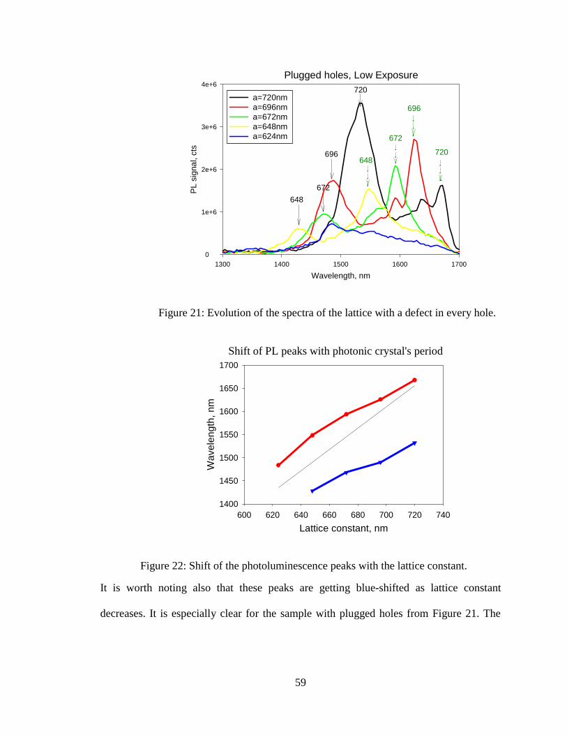
59
It is worth noting also that these peaks are getting blue-shifted as lattice constant
decreases. It is especially clear for the sample with plugged holes from Figure 21. The
Plugged holes, Low Exposure
Wavelength, nm
1300 1400 1500 1600 1700
PL
sign
al, c
ts
0
1e+6
2e+6
3e+6
4e+6
a=720nm a=696nma=672nma=648nma=624nm
720
696
672
648
720
696
648
672
Figure 21: Evolution of the spectra of the lattice with a defect in every hole.
Shift of PL peaks with photonic crystal's period
Lattice constant, nm600 620 640 660 680 700 720 740
Wav
elen
gth,
nm
1400
1450
1500
1550
1600
1650
1700
Figure 22: Shift of the photoluminescence peaks with the lattice constant.
60
wavelengths of the major PL peaks for this sample set are plotted versus lattice constant
in Figure 22. The wavelengths versus lattice constant nearly follow a straight line. It can
be seen also that the spectral shape evolves gradually, with respect to the lattice constant.
The complicated structure of the PL spectra in Figures 20 and 21 is a good evidence of
the spontaneous emission modification.
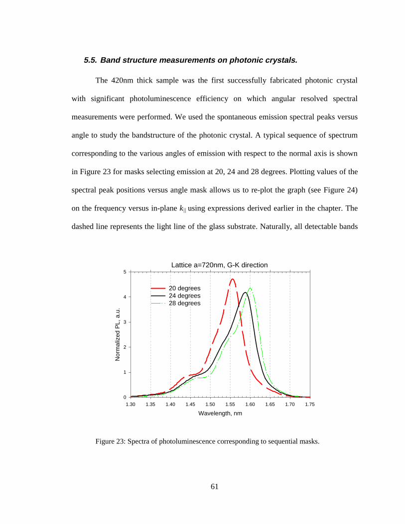
61
Lattice a=720nm, G-K direction
Wavelength, nm
1.30 1.35 1.40 1.45 1.50 1.55 1.60 1.65 1.70 1.75
Nor
mal
ized
PL,
a.u
.
0
1
2
3
4
5
20 degrees24 degrees28 degrees
Figure 23: Spectra of photoluminescence corresponding to sequential masks.
5.5. Band structure measurements on photonic crystals.
The 420nm thick sample was the first successfully fabricated photonic crystal
with significant photoluminescence efficiency on which angular resolved spectral
measurements were performed. We used the spontaneous emission spectral peaks versus
angle to study the bandstructure of the photonic crystal. A typical sequence of spectrum
corresponding to the various angles of emission with respect to the normal axis is shown
in Figure 23 for masks selecting emission at 20, 24 and 28 degrees. Plotting values of the
spectral peak positions versus angle mask allows us to re-plot the graph (see Figure 24)
on the frequency versus in-plane k|| using expressions derived earlier in the chapter. The
dashed line represents the light line of the glass substrate. Naturally, all detectable bands
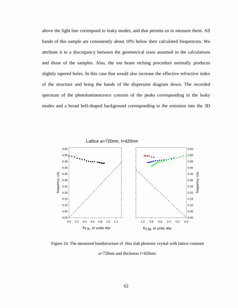
62
above the light line correspond to leaky modes, and that permits us to measure them. All
bands of this sample are consistently about 10% below their calculated frequencies. We
attribute it to a discrepancy between the geometrical sizes assumed in the calculations
and those of the samples. Also, the ion beam etching procedure normally produces
slightly tapered holes. In this case that would also increase the effective refractive index
of the structure and bring the bands of the dispersion diagram down. The recorded
spectrum of the photoluminescence consists of the peaks corresponding to the leaky
modes and a broad bell-shaped background corresponding to the emission into the 3D
KΓΚ, in units π/a,0.0 0.2 0.4 0.6 0.8 1.0 1.2
freq
uenc
y, c
/a
0.00
0.05
0.10
0.15
0.20
0.25
0.30
0.35
0.40
0.45
0.50
0.55
Lattice a=720nm, t=420nm
KΓΜ, in units π/a,
0.00.20.40.60.81.0
freq
uenc
y, c
/a
0.00
0.05
0.10
0.15
0.20
0.25
0.30
0.35
0.40
0.45
0.50
0.55
Figure 24. The measured bandstructure of thin slab photonic crystal with lattice constant
a=720nm and thickness t=420nm.
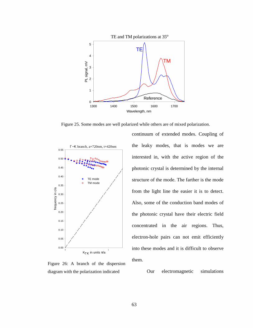
63
continuum of extended modes. Coupling of
the leaky modes, that is modes we are
interested in, with the active region of the
photonic crystal is determined by the internal
structure of the mode. The farther is the mode
from the light line the easier it is to detect.
Also, some of the conduction band modes of
the photonic crystal have their electric field
concentrated in the air regions. Thus,
electron-hole pairs can not emit efficiently
into these modes and it is difficult to observe
them.
Our electromagnetic simulations
TE and TM polarizations at 35o
Wavelength, nm
1300 1400 1500 1600 1700
PL
sign
al, m
V
0
1
2
3
4
5
TE
TM
Reference
Figure 25. Some modes are well polarized while others are of mixed polarization.
Γ−Κ branch, a=720nm, t=420nm
KΓΚ in units π/a0 1
freq
uenc
y in
c/a
0.00
0.05
0.10
0.15
0.20
0.25
0.30
0.35
0.40
0.45
0.50
0.55
TE modeTM mode
Figure 26: A branch of the dispersion
diagram with the polarization indicated
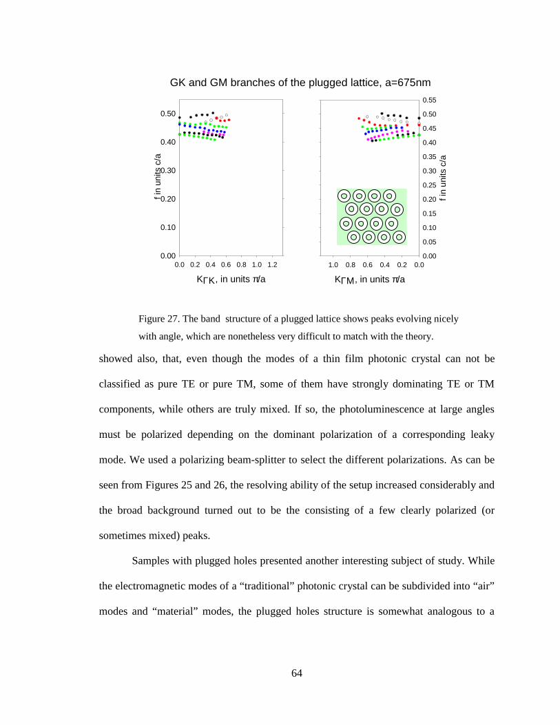
64
showed also, that, even though the modes of a thin film photonic crystal can not be
classified as pure TE or pure TM, some of them have strongly dominating TE or TM
components, while others are truly mixed. If so, the photoluminescence at large angles
must be polarized depending on the dominant polarization of a corresponding leaky
mode. We used a polarizing beam-splitter to select the different polarizations. As can be
seen from Figures 25 and 26, the resolving ability of the setup increased considerably and
the broad background turned out to be the consisting of a few clearly polarized (or
sometimes mixed) peaks.
Samples with plugged holes presented another interesting subject of study. While
the electromagnetic modes of a “traditional” photonic crystal can be subdivided into “air”
modes and “material” modes, the plugged holes structure is somewhat analogous to a
KΓΚ, in units π/a
0.0 0.2 0.4 0.6 0.8 1.0 1.2
f in
units
c/a
0.00
0.10
0.20
0.30
0.40
0.50
GK and GM branches of the plugged lattice, a=675nm
KΓΜ, in units π/a
0.00.20.40.60.81.0
f in
units
c/a
0.00
0.05
0.10
0.15
0.20
0.25
0.30
0.35
0.40
0.45
0.50
0.55
Figure 27. The band structure of a plugged lattice shows peaks evolving nicely
with angle, which are nonetheless very difficult to match with the theory.
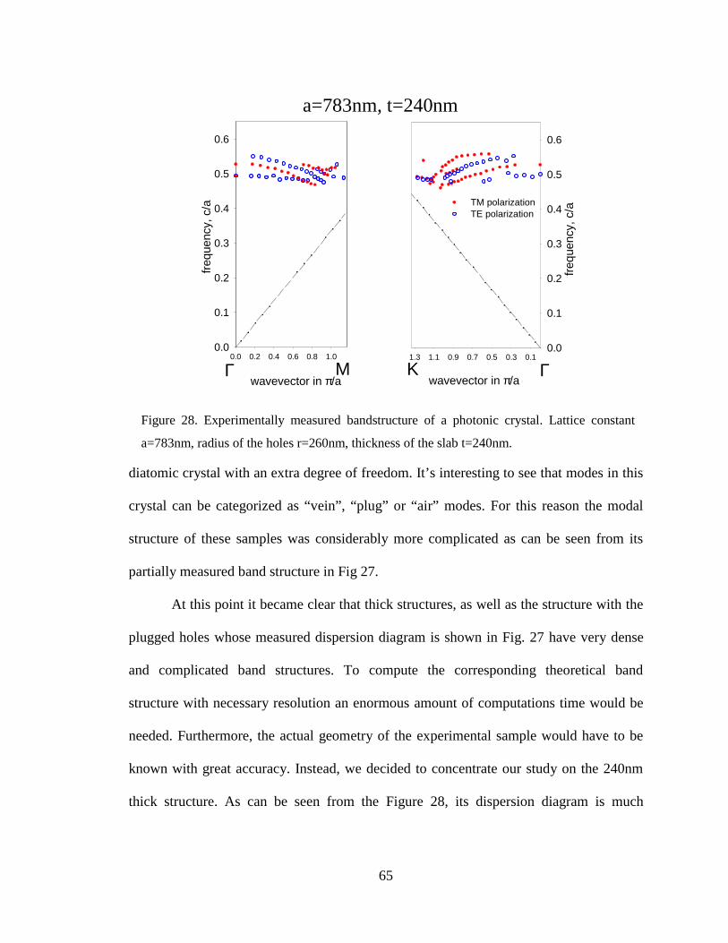
65
diatomic crystal with an extra degree of freedom. It’s interesting to see that modes in this
crystal can be categorized as “vein”, “plug” or “air” modes. For this reason the modal
structure of these samples was considerably more complicated as can be seen from its
partially measured band structure in Fig 27.
At this point it became clear that thick structures, as well as the structure with the
plugged holes whose measured dispersion diagram is shown in Fig. 27 have very dense
and complicated band structures. To compute the corresponding theoretical band
structure with necessary resolution an enormous amount of computations time would be
needed. Furthermore, the actual geometry of the experimental sample would have to be
known with great accuracy. Instead, we decided to concentrate our study on the 240nm
thick structure. As can be seen from the Figure 28, its dispersion diagram is much
wavevector in π/a
0.0 0.2 0.4 0.6 0.8 1.0
freq
uenc
y, c
/a
0.0
0.1
0.2
0.3
0.4
0.5
0.6
a=783nm, t=240nm
wavevector in π/a
0.10.30.50.70.91.11.3
freq
uenc
y, c
/a
0.0
0.1
0.2
0.3
0.4
0.5
0.6
Γ Κ ΓΜ
TE polarizationTM polarization
Figure 28. Experimentally measured bandstructure of a photonic crystal. Lattice constant
a=783nm, radius of the holes r=260nm, thickness of the slab t=240nm.
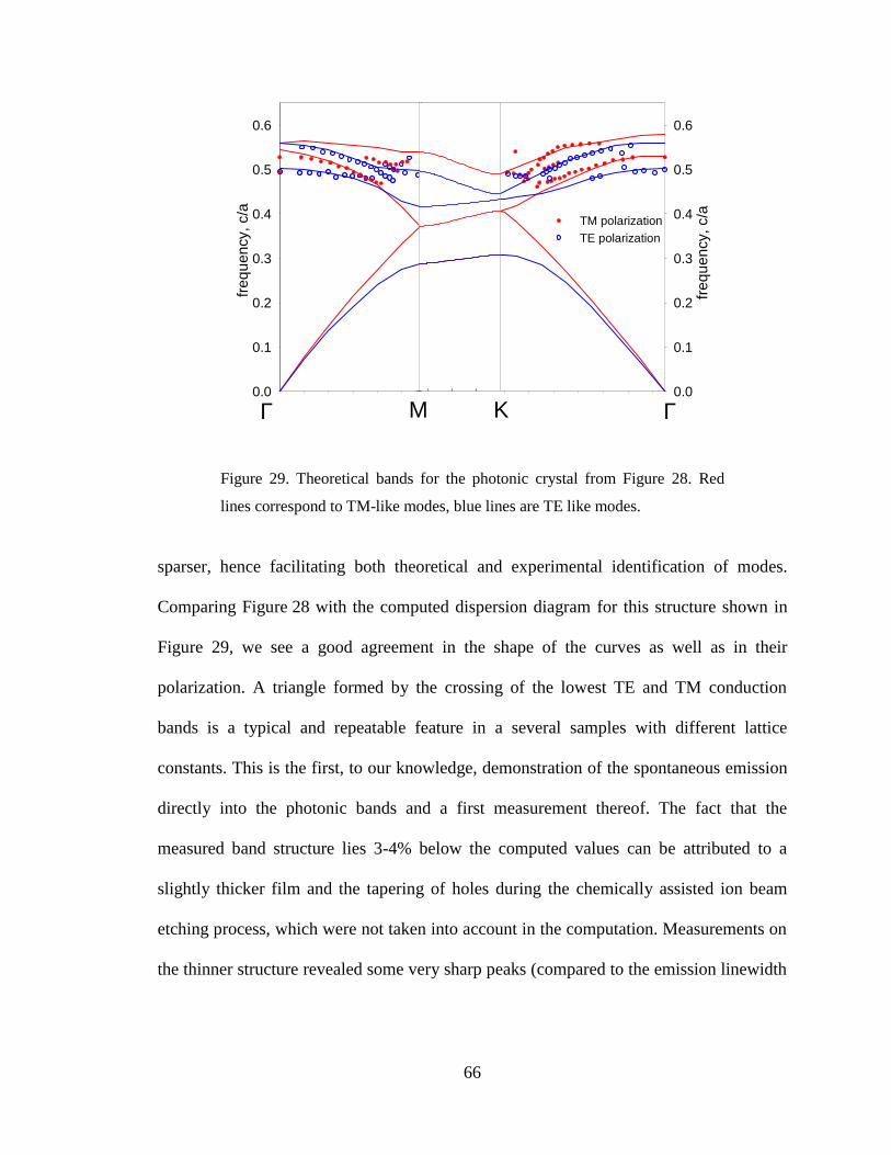
66
sparser, hence facilitating both theoretical and experimental identification of modes.
Comparing Figure 28 with the computed dispersion diagram for this structure shown in
Figure 29, we see a good agreement in the shape of the curves as well as in their
polarization. A triangle formed by the crossing of the lowest TE and TM conduction
bands is a typical and repeatable feature in a several samples with different lattice
constants. This is the first, to our knowledge, demonstration of the spontaneous emission
directly into the photonic bands and a first measurement thereof. The fact that the
measured band structure lies 3-4% below the computed values can be attributed to a
slightly thicker film and the tapering of holes during the chemically assisted ion beam
etching process, which were not taken into account in the computation. Measurements on
the thinner structure revealed some very sharp peaks (compared to the emission linewidth
freq
uenc
y, c
/a
0.0
0.1
0.2
0.3
0.4
0.5
0.6
freq
uenc
y, c
/a
0.0
0.1
0.2
0.3
0.4
0.5
0.6
Γ Κ ΓΜ
TE polarizationTM polarization
Figure 29. Theoretical bands for the photonic crystal from Figure 28. Red
lines correspond to TM-like modes, blue lines are TE like modes.
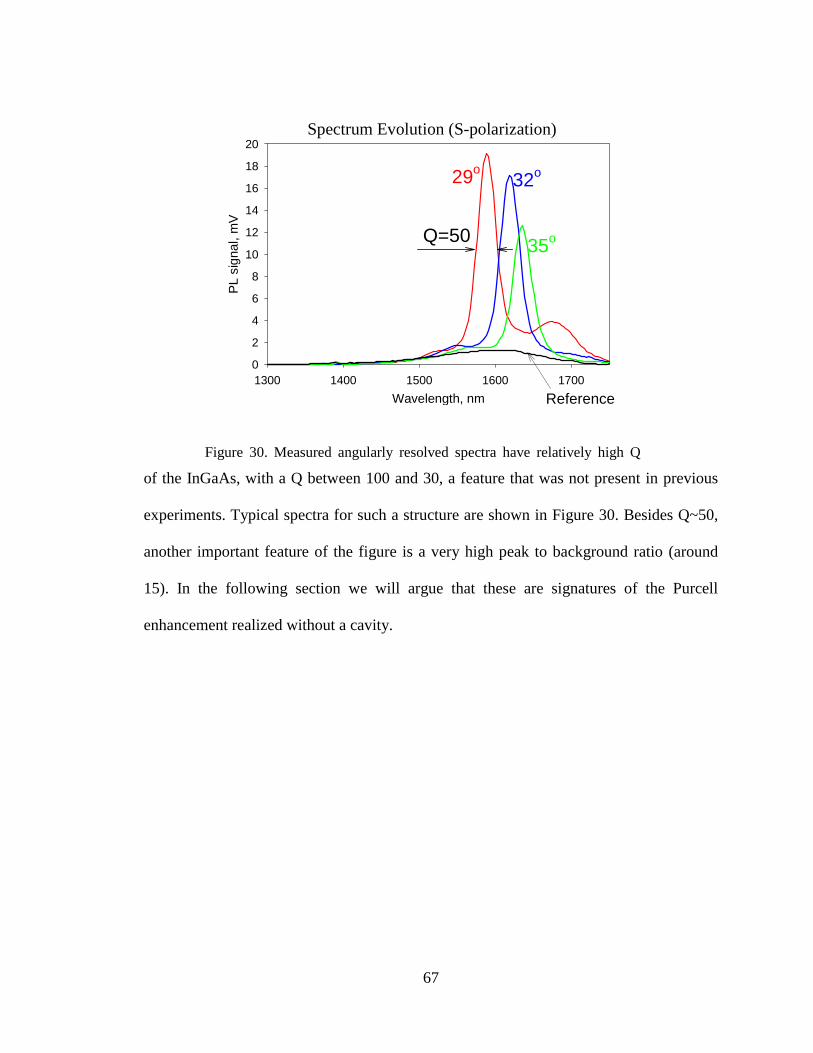
67
of the InGaAs, with a Q between 100 and 30, a feature that was not present in previous
experiments. Typical spectra for such a structure are shown in Figure 30. Besides Q~50,
another important feature of the figure is a very high peak to background ratio (around
15). In the following section we will argue that these are signatures of the Purcell
enhancement realized without a cavity.
Spectrum Evolution (S-polarization)
Wavelength, nm
1300 1400 1500 1600 1700
PL
sign
al, m
V
0
2
4
6
8
10
12
14
16
18
20
32o
35o
Reference
29o
Q=50
Figure 30. Measured angularly resolved spectra have relatively high Q
68
5.6. Resonant enhancement in thin-slab photonic crystals
It was shown in the chapter 2 that spontaneous emission in a small cavity happens faster
than in the bulk material. Crucial parameters for the speedup were cavity Q and effective
volume Veff of the resonant mode:
( )eff
m
V
ngQ
πλ
2
2/3 3
0
=ΓΓ
(47)
In the photonic crystals studied in the previous section, the measured Q’s of modes were
comparable to that of a dielectric cavity. Since these modes are large in volume, local
field enhancement is much smaller. But since the band structure of upper modes is nearly
flat as can be seen from both theoretical and experimental results (Figures 28 and 29),
these modes pick up a large degeneracy factor, g, compensating the loss in the local field
enhancement.
Now we will derive the enhancement of spontaneous emission in a particular direction:
Suppose we have selected a narrow solid angle sinθdθdφ and a frequency range dω.
Then, similarly to the derivation in Chapter 3, we have to compare the density of modes
and local fields of the emission into a 3-d continuum of modes to that of the emission into
the leaky guided modes.
The spontaneous emission rate is proportional to the local field of the mode E2(r )
(normalized to hν/2) and to the number of modes ∆N emitting into the given solid angle
in given frequency range.
For emission into the 3-d continuum of modes,
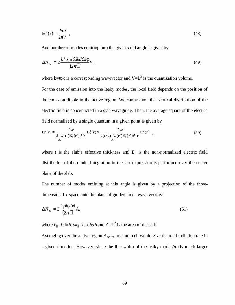
69
nV2)(2 ω!=rE , (48)
And number of modes emitting into the given solid angle is given by
( )V
ddkdkN d 3
2
32
sin2
πφθθ
=∆ , (49)
where k=ω/c is a corresponding wavevector and V=L3 is the quantization volume.
For the case of emission into the leaky modes, the local field depends on the position of
the emission dipole in the active region. We can assume that vertical distribution of the
electric field is concentrated in a slab waveguide. Then, the average square of the electric
field normalized by a single quantum in a given point is given by
)(')'()'()2/(2
)(')'()'(2
)( 2022
0
2032
0
2 rErrEr
rErrEr
rE∫∫
≈=
slabslab
dtd εω
εω !!
, (50)
where t is the slab’s effective thickness and E0 is the non-normalized electric field
distribution of the mode. Integration in the last expression is performed over the center
plane of the slab.
The number of modes emitting at this angle is given by a projection of the three-
dimensional k-space onto the plane of guided mode wave vectors:
( ) Addkk
N d 2
||||3
22
πφ
=∆ , (51)
where k||=ksinθ, dk||=kcosθdθ and A=L2 is the area of the slab.
Averaging over the active region Aactive in a unit cell would give the total radiation rate in
a given direction. However, since the line width of the leaky mode ∆ω is much larger
70
than specified spectral resolution dω, only ωω
π ∆d2
of the radiation will be in the spectral
range. The 2/π pre-factor comes from the Lorentzian lineshape of the leaky mode, similar
to the derivation in Chapter 3.
Thus, rate of background radiation would be given by
( ) active
active
dd AnV
Vddkdk
rdN ⋅⋅=∆∝Γ ∫ 22
sin2)( 3
22
32
3
ωπ
φθθ !rE (52)
And, in the same way, emission into the leaky modes is
( ) rdAddkkd
dtrdN
active
slab
active
dd22
02220
22
22 )(
2
)cos)(sin(2
')'()'()2/(2)( ∫∫∫ ∆
⋅=∆∝Γ rErrEr
rEπ
φθθθωπω
εω! (53)
Taking a ratio and simplifying we get:
θλω
ωε
επcos
)(
')'()'(
122
0
2203
2
ntA
rd
d
A
active
active
slab
slab
d
d ⋅∆
⋅⋅=ΓΓ ∫
∫
rE
rrEr. (54)
Introducing mode’s Q=ω/∆ω, and a parameter γ to characterize electric energy overlap
with the active region:
active
active
slab
slab
A
d
d
ArrE
rrEr
220
220
)(
')'()'(
∫∫
⋅=ε
εγ (55)
enhancement of spontaneous emission rate at a given frequency can be transformed into a
familiar structure of a Purcell number in 1 dimension:
θλπγω
cos2
2)(
3
2
ntQ
d
d ⋅=Γ
Γ (56)
71
In semiconductors, the emission band is normaly wider than the cavity linewidth. For that
reason Lorentizan in Equation (56) has to be convolved with the semiconductor emission
spectrum, as it was done in derivation of Equation (24). This integrates out the 2/π in the
Lorentzian and substitutes Q with the material’s Qm (10 for InGaAs in our case). Then
spectrally integrated enhancement in a given direction becomes
θλγ cos23
2
ntQm
d
d ⋅=ΓΓ
(57)
In the structure we have studied, the active region covers approximately half of the
sample area. In the optimal case, when all electric energy of the mode is concentrated in
the semiconductor, the overlap parameter is simpl y γ≈2. This happens close to the Γ
point of the Brillouin zone, as can be seen from the computed energy distribution plot in
Figure 31. Then, expected peak enhancement, i.e the peak to background ratio of the
spectra in Figure 30, in a direction close to the normal would be QQd
d ≈⋅
⋅⋅≤ΓΓ
2407
165022
3
2
π ,
i.e. approximately the modal Q. The
observed peak to background ratio is
smaller, about 15 to 20. We attribute
this discrepancy to two factors: First,
the background may be higher due to
the contribution of other modal peaks,
and, second, the structure
imperfections may cause some
Figure 31. Electric energy distribution in the Γ
point of the Brillouin zone. All energy is
concentrated in the dielectric veins.
72
additional scattering of the mode.
If the photonic bands could be engineered to be flat compared to the frequency variation
across the Brillouin zone, this enhancement would be almost the same for all directions.
As can be seen from the experimental and theoretical band structures of the photonic
crystal that we considered, the variation of the lowest “conduction” band is
approximately twice the spontaneous emission band. Then intergrated over all the angles,
the enhancement becomes much smaller, between 3 and five. If the band can be made
flat, the radiative lifetime can be made substantially shorter.
In the best of the thin slab photonic crystals, the photoluminescence efficiency
was considerably greater than in unpatterned samples. Absolute efficiency calibration can
be made by referencing the emission to the reflection (100%) froom a white surface.
Such calibration generally show that InGaAs double heterostructures grown by raj Bhat,
have an internal quantum efficiency near 100%.
An unpatterned thin film between two glass hemispheres has an optical escape
probability of 11.0~)/(4
12
2gf nn , where nf=3.2 and ng=1.5 are refractive indices of the
semiconductor film and glass correspondingly. In our ultra-thin films, the effective
refractive index is probably slightly smaller than that of the bulk material. Also, the high
internal efficiency of the InGaAs active layer allows the photon recycling to boost the
external efficiency of the film even higher. With all these benefits combined, we
conservatively estimate that a thin film, when encapsulated in glass, can have 12-14%
external efficiency. This sets an absolute efficiency scale for the photonic crystal samples
shown in the Figure 32b, which were all measured under identical pump and collection
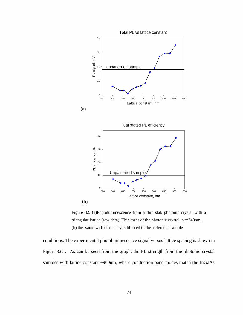
73
conditions. The experimental photoluminescence signal versus lattice spacing is shown in
Figure 32a . As can be seen from the graph, the PL strength from the photonic crystal
samples with lattice constant ~900nm, where conduction band modes match the InGaAs
(a)
Total PL vs lattice constant
Lattice constant, nm550 600 650 700 750 800 850 900 950
PL
sign
al, m
V0
10
20
30
40
Unpatterned sample
(b)
Calibrated PL efficiency
Lattice constant, nm550 600 650 700 750 800 850 900 950
PL
effic
ienc
y, %
0
12
24
36
48
Unpatterned sample
Figure 32. (a)Photoluminescence from a thin slab photonic crystal with a
triangular lattice (raw data). Thickness of the photonic crystal is t=240nm.
(b) the same with efficiency calibrated to the reference sample
74
emission frequency, is twice as large as that from an unpatterned sample. Taking into
account that there is only half as much surface area in the patterned PBG samples to
absorb light (at least in the geometrical optics approximation), this gives the external
efficiency of 48-56%.There are three factors influencing the measured external quantum
efficiency of photonic crystal samples:
1. In principle, the extraction efficiency can be unity since all modes are leaky.
2. By drilling the holes through the active region, we introduce a non-radiative
recombination. We will show below that non-radiative recombination rate N is
comparable to the radiative emission rate R: N/R~1, where R is the radiative emission
rate in bulk semiconductor material in which there is no Purcell effect.
3. The radiative emission rate in the patterned film is enhanced by the Purcell
factor F, a quantity we would like to determine: R→FR.
Then, the external quantum efficiency of the sample emitting into the conduction
band modes of the photonic crystal would be given by the fractional rates:
RNF
F
NFR
FR
/+=
+=η , (58)
which can be solved for the Purcell enhancement factor F:
R
NF ⋅
−=
ηη
1 (59)
It follows from the Equation (59) that the knowledge of non-radiative
recombination rate is necessary to determine the Purcell factor.
We can use the 600-700nm samples emitting into the forbidden photonic bandgap
to estimate the non-radiative recombination rate. Indeed, as can be seen from the
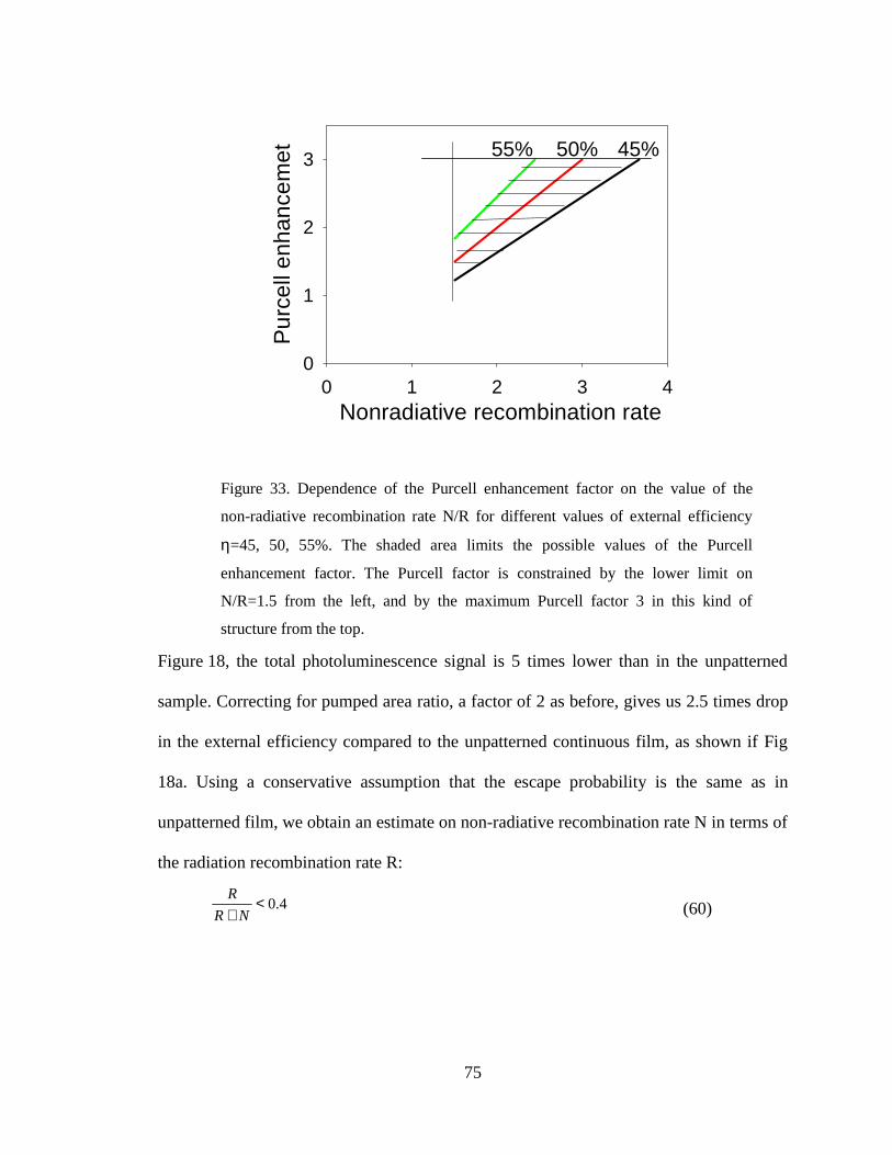
75
Figure 18, the total photoluminescence signal is 5 times lower than in the unpatterned
sample. Correcting for pumped area ratio, a factor of 2 as before, gives us 2.5 times drop
in the external efficiency compared to the unpatterned continuous film, as shown if Fig
18a. Using a conservative assumption that the escape probability is the same as in
unpatterned film, we obtain an estimate on non-radiative recombination rate N in terms of
the radiation recombination rate R:
4.0<+ NR
R(60)
N/R=3
2
1
Nonradiative recombination rate0 1 2 3 4
Pur
cell
enha
ncem
et
0
1
2
3 55% 50% 45%
Figure 33. Dependence of the Purcell enhancement factor on the value of the
non-radiative recombination rate N/R for different values of external efficiency
η=45, 50, 55%. The shaded area limits the possible values of the Purcell
enhancement factor. The Purcell factor is constrained by the lower limit on
N/R=1.5 from the left, and by the maximum Purcell factor 3 in this kind of
structure from the top.
76
from which follows N/R>1.5. This implies a nonradiative recombination velocity
S>20000cm/s, since the absolute rate R is known to be R=1/τ=Bn with B=5 10-10cm3/s
and n=1018cm-3, which is consistent with out previous measurement on surface
recombination velocity.
The factor 1.5 is a lower limit on the non-radiative/radiative recombination rate because
the extraction efficiency of the sample with holes is more likely to increase due to the
presence of additional surfaces. Plotted in Figure 33, is a family of curves showing the
dependence of Purcell enhancement factor versus (N/R) for different efficiencies from
Eqn. (59). As one can see from the Figure 33, the Purcell factor is constrained by our
measurements to be above 1.5 but less than the ideal Purcell factor 3 which would occur
in the ideal case.
Certainly, we will need to perform lifetime measurements on our samples to verfy
the exact value of the Purcell factor for spontaneous emission into conduction band
modes.
The expressions for Purcell factor obtained in this section resemble the results for
the VCSEL-type structures, the only difference is in the number of resonant modes. In the
VCSEL structures the resonator is comprised of a pair of mirrors while in our case the
structure provides a standing wave due to its periodicity. Unlike the microcavities with
tiny mode volume and correspondingly small active region that we considered in the
Chapter 3, the flat photonic conduction bands relatively to the broad emission spectra at
room temperature, makes the control over spontaneous emission technologically possible.
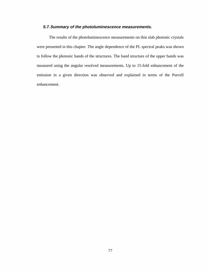
77
5.7. Summary of the photoluminescence measurements.
The results of the photoluminescence measurements on thin slab photonic crystals
were presented in this chapter. The angle dependence of the PL spectral peaks was shown
to follow the photonic bands of the structures. The band structure of the upper bands was
measured using the angular resolved measurements. Up to 15-fold enhancement of the
emission in a given direction was observed and explained in terms of the Purcell
enhancement.
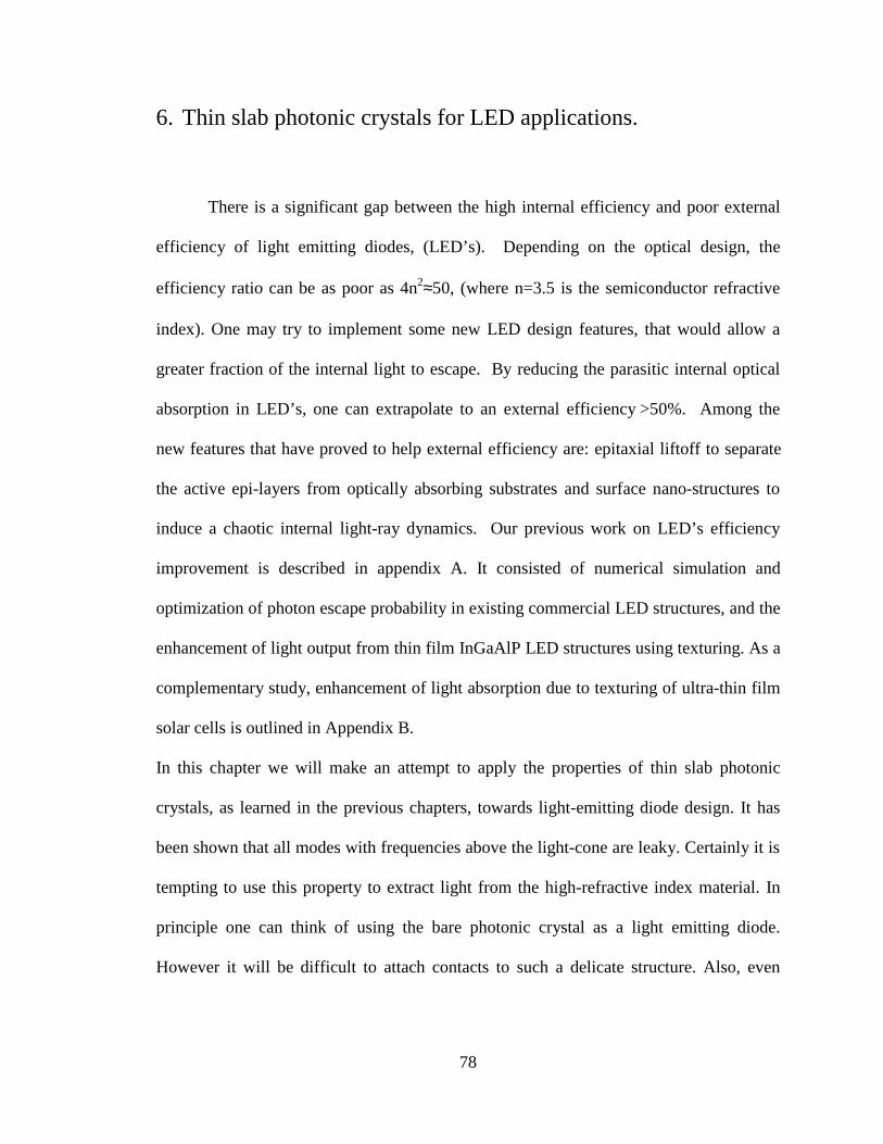
78
6. Thin slab photonic crystals for LED applications.
There is a significant gap between the high internal efficiency and poor external
efficiency of light emitting diodes, (LED’s). Depending on the optical design, the
efficiency ratio can be as poor as 4n2≈50, (where n=3.5 is the semiconductor refractive
index). One may try to implement some new LED design features, that would allow a
greater fraction of the internal light to escape. By reducing the parasitic internal optical
absorption in LED’s, one can extrapolate to an external efficiency >50%. Among the
new features that have proved to help external efficiency are: epitaxial liftoff to separate
the active epi-layers from optically absorbing substrates and surface nano-structures to
induce a chaotic internal light-ray dynamics. Our previous work on LED’s efficiency
improvement is described in appendix A. It consisted of numerical simulation and
optimization of photon escape probability in existing commercial LED structures, and the
enhancement of light output from thin film InGaAlP LED structures using texturing. As a
complementary study, enhancement of light absorption due to texturing of ultra-thin film
solar cells is outlined in Appendix B.
In this chapter we will make an attempt to apply the properties of thin slab photonic
crystals, as learned in the previous chapters, towards light-emitting diode design. It has
been shown that all modes with frequencies above the light-cone are leaky. Certainly it is
tempting to use this property to extract light from the high-refractive index material. In
principle one can think of using the bare photonic crystal as a light emitting diode.
However it will be difficult to attach contacts to such a delicate structure. Also, even
79
though the photoluminescence from the photonic crystals studied in Chapter 5 is larger
than in a planar sample, it would be much better to have an active region free from the
non-radiative surface recombination losses. In other words, it is a reasonable idea to
separate regions where the light is extracted from those where the light is generated. The
structure shown in Fig. 34 is a hexagon of unetched material surrounded by the photonic
crystal. The light is generated in the center region, small 1/2n2 fraction of it is emitted and
the rest is trapped in the waveguide. It is easy to estimate that the re-absorption length in
the 0.4µm thick film, with a 200Å active region, is about 15µm. In high-quality
materials, this length can be even larger due to the re-emission process. If the dimensions
of the photonic crystal are chosen such that spontaneous emission band of the active
Figure 34. A schematic of an LED structures. The structure consists of an
unetched region surrounded by a thin slab photonic crystal, which scatters
guided light. into the space.
80
material overlaps with the leaking modes of the photonic conduction band the light can
be efficiently scattered out of the semiconductor. The leakage length of the guided modes
has to be shorter than re-absorption length in the photonic crystal. Voids reduce the
effective absorption of the photonic crystal, and the leakage length of conduction band
modes decreases as the bands move up away from the escape cone. Thus, for sufficiently
large lattice spacing guided modes can escape before being re-absorbed.
In these experiments, we compared spontaneous emission from an unpatterned
optically pumped region surrounded by a few rows of photonic crystal. The lattice
spacing, a, of the photonic crystal was 600, 760 or 900nm. According to our band
wavelength, nm
1300 1400 1500 1600 1700
PL
sign
al, m
V
0
20
40
60
80
100
900nm
760nm
600nm
Reference
Figure 35. Angle-integrated spectra of the LED structure. The peak
wavelength is red-shifted for larger lattice constants.
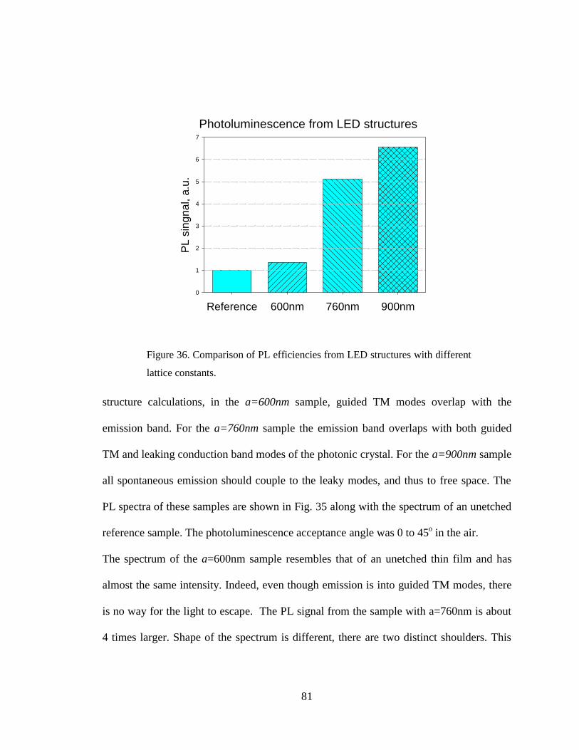
81
structure calculations, in the a=600nm sample, guided TM modes overlap with the
emission band. For the a=760nm sample the emission band overlaps with both guided
TM and leaking conduction band modes of the photonic crystal. For the a=900nm sample
all spontaneous emission should couple to the leaky modes, and thus to free space. The
PL spectra of these samples are shown in Fig. 35 along with the spectrum of an unetched
reference sample. The photoluminescence acceptance angle was 0 to 45o in the air.
The spectrum of the a=600nm sample resembles that of an unetched thin film and has
almost the same intensity. Indeed, even though emission is into guided TM modes, there
is no way for the light to escape. The PL signal from the sample with a=760nm is about
4 times larger. Shape of the spectrum is different, there are two distinct shoulders. This
Photoluminescence from LED structures
Reference 600nm 760nm 900nm
PL
sing
nal,
a.u.
0
1
2
3
4
5
6
7
Figure 36. Comparison of PL efficiencies from LED structures with different
lattice constants.
82
measurement was done without angular resolution, so some finer spectral features may be
missing.
Finally, the sample with the a=900nm hole spacing showed even higher overall
efficiency. It is worth noting, that in this measurement, only the unpatterned center area
was pumped, and thus pumping condition remained identical for all samples. The
spectrally integrated areas are summarized in Figure 36. More than six-fold improvement
in light extraction was achieved using the photonic crystal around the edges of an active
semiconductor film. This result on periodic structures complements the previous work on
random texturing described in Appendix B. One of the advantages of photonic crystals is
that, due to the coherent scattering, they provide a shorter escape length. That means that
this method can be used in materials with internal quantum efficiencies too low to
tolerate re-absorption.
83
7. Summary
Let me summarize the work described in this thesis:
We studied experimentally and theoretically the modification of spontaneous
emission in semiconductor photonic crystals at room temperature. Small material Qm of
semiconductors together with the large surface recombination velocities make
observation of these effects an interesting and challenging task.
A quantum electro-dynamical model was developed to estimate enhancement of
spontaneous radiation rates in photonic crystals and microcavities. Extensive numerical
computations were employed to calculate the band structure of thin slab photonic crystals
and modal properties of microcavities. The minimal effective mode volume, a parameter
crucial for cavity enhancement of spontaneous emission was found to be 2(λ/2n)3 where
λ is the resonant wavelength and n is the refractive index. A possible 5-fold enhancement
of spontaneous emission rate (Purcell effect) was shown to be possible in InGaAs
microcavities at room temperature under the most optimistic conditions.
Photoluminescence measurements were used in the search of the material system
most suitable for fabrication of such a photonic crystal. It was shown that the InGaAs/InP
and InGaN material systems are good candidates for opto-electronically active photonic
bandgap structures.
Angularly resolved photoluminescence measurements were used to measure
experimentally the band structure of conductions band of such a photonic crystal and
overall enhancement of spontaneous emission.
84
Spontaneous emission enhancement in thin slab photonic crystals was
demonstrated. It was shown that emission into the leaky conduction bands of the crystal
has the same effect as cavity-enhanced spontaneous emission provided these bands are
flat enough relative to the emission band of the material.
Structures described in Chapters 5 and 6 have a good potential to be used in real-
world light-emitting diode designs. Issues of ohmic contacts and packaging were not
addressed in this work, although these are important aspects of a final product
fabrication.
Recommendations for novel LED designs were worked out based on the results of
this study.
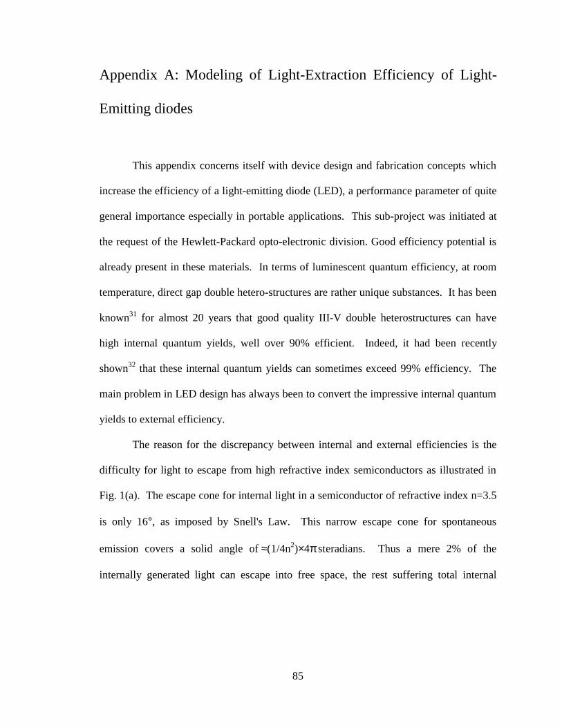
85
Appendix A: Modeling of Light-Extraction Efficiency of Light-
Emitting diodes
This appendix concerns itself with device design and fabrication concepts which
increase the efficiency of a light-emitting diode (LED), a performance parameter of quite
general importance especially in portable applications. This sub-project was initiated at
the request of the Hewlett-Packard opto-electronic division. Good efficiency potential is
already present in these materials. In terms of luminescent quantum efficiency, at room
temperature, direct gap double hetero-structures are rather unique substances. It has been
known31 for almost 20 years that good quality III-V double heterostructures can have
high internal quantum yields, well over 90% efficient. Indeed, it had been recently
shown32 that these internal quantum yields can sometimes exceed 99% efficiency. The
main problem in LED design has always been to convert the impressive internal quantum
yields to external efficiency.
The reason for the discrepancy between internal and external efficiencies is the
difficulty for light to escape from high refractive index semiconductors as illustrated in
Fig. 1(a). The escape cone for internal light in a semiconductor of refractive index n=3.5
is only 16°, as imposed by Snell's Law. This narrow escape cone for spontaneous
emission covers a solid angle of ≈(1/4n2)×4π steradians. Thus a mere 2% of the
internally generated light can escape into free space, the rest suffering total internal
86
reflection and risking re-absorption. An unsophisticated LED design would be only 2%
externally efficient, even when the internal efficiency is 100%.
There is no easy solution to the total internal reflection problem. For example, if
an anti-reflection coating is applied to the semiconductor surface, then the escape cone
would apparently be broadened. But then
there would be a second escape cone from
the coating material into free space as
illustrated in Fig. 1(b). Some of the rays
would escape from the semiconductor only
to be trapped by the anti-reflection coating.
The net effect of a 2-fold hierarchy of
escape cones is that the same fraction
(1/4n2)×4π steradians of the light manages
to escape. The determining parameter is
the overall refractive index ratio (n÷1)
between medium in which the light is
generated, and the medium where we want
the light to end up, (free space).
It is paradoxical that total internal
reflection can co-exist with an anti-
reflection coating. Indeed the anti-
reflection coating has no net effect on the
Figure A1: (a) Transmission of light within
the escape cone. (b) In the presence of an
anti-reflection coating, there are two
successive escape cones, but net escape
angle is the same as in (a).
87
overall total internal reflection. An anti-reflection coating merely reduces the Fresnel
reflectivity for those rays inside the narrow escape cone, rays which are capable of
escaping in any case. On the other hand, those rays outside the escape cone are totally
internally reflected irrespective of any thin coating on the surface.
To effectively address the problem of the narrow escape cone requires a change in
the geometry of the high index material. Early on, it was recognized that a hemispherical
dome33 made of high index semiconductor material, centered on the LED, would allow
all the light to exit the surface at normal incidence. Unfortunately, a lens made of low
index material such as epoxy, is only partially and incompletely effective.
Until now, the cost of a hemispherical semiconductor lens has been such that they
have not been used commercially. Instead, a different physical principle allows light to
escape from inside an LED. This principle, of chaotic propagation of light, is illustrated
in Fig. 2. The idea is that a light ray experiencing chaotic dynamics inside a
semiconductor will eventually find the escape cone. Sometimes this form of optics34 is
called “Statistical Ray Optics”, and it was originally developed for understanding the
trapping of light inside solar cells. Today, all record-breaking solar cells make use35 of
this concept. An LED is an inverse solar cell, and similar ideas were put forth for LED’s
by Joyce et al36 over two decades ago.
In a plane parallel semiconductor sheet light is spontaneously emitted beyond the
angle of total internal reflection. Such internally reflected light bounces back and forth
endlessly between the two surfaces, never escaping. If one of the surfaces is textured, the
light ray direction is randomized with each reflection off the textured surface. Each such
88
random reflection allows a 2% probability that the light will happen to catch the escape
cone on the next pass. In this way the light eventually escapes. Chaotic dynamics is
simply restored by a deviation from perfect symmetry, allowing internally generated light
to escape! The lesson is break the symmetry and you will help the LED efficiency. An
intentional texture on the semiconductor surfaces of the LED is one of the simplest ways
of helping the light to escape.
1. Statement of Problem.
The chaotic dynamics approach for allowing light to escape from an LED imposes
certain design requirements. The most important is, the long internal path length
required, before the light escapes. Given the (1/4n2)≈1/50 probability of escaping per
surface reflection, the internal path length is required to be at least 50 times larger than
the thickness of the semiconductor. Thus the main requirement for high LED efficiency,
once chaotic dynamics is achieved, is a very low parasitic absorption as the light scatters
around internally in the device. Optical design for low parasitics emerges as one of the
main requirements for LED efficiency. Indeed one of the worst practices is to build an
LED on optically absorbing substrate, e.g. a visible LED on a GaAs substrate. There is a
current trend toward transparent superstrates and transparent substrates, by strained
hetero-epitaxy37 and by wafer bonding38 respectively.
The leading manufacturers such as HP have commercialized red LED’s having
external efficiencies above 20%, and occasionally reaching 30%. These high brightness
LED’s represent a major improvement over the original generation of LED’s, but there is
room for further optical sophistication in getting the light out of these materials.
89
2. Photon gas simulations
A model of optical processes in LED’s was created that takes into account device
geometry, light absorption in contacts and cladding layers, photon recycling, light
randomization due to surface scattering and the benefit from encapsulation of the device
into epoxy. Here we report results of the light extraction efficiency modeling using the
photon gas method and Monte-Carlo simulations.
Based on the results of our modeling, an optimized LED design was proposed.
Also, to determine parameters for the model, photoluminescence measurements of
internal quantum efficiency were performed on the epi-layers used for LED fabrication.
A photon gas model37 based on the statistical properties of the completely
randomized photons in the semiconductor device, allows one to make estimates of the
dependence of the LED light extraction efficiency. This will depend on quality of the
active layer material and geometric parameters such as aspect ratio and thickness of
active layer. We consider a square chip with dimensions width L and height H, with the
active layer of thickness d in the middle and reflecting electrical contacts on the top and
bottom surfaces covering area Acontact. Top and bottom surfaces are assumed to be
polished while four side edges are rough saw-cut. This design is similar to that used by
HP Opto-Electronics Division in fabrication of visible LED’s based on InGaAlP
quaternary alloys38, with L~200µm, H~250µm and d~1µm.
The photon flux inside the LED is:
I=[Density of photons inside LED]⋅c
n,
90
where n is the refractive index of the semiconductor,
There are four ways for a photon to disappear from an LED:
a) For the portion of photon whose direction falls in the escape cone, the escape rate will
be proportional to the surface area and the escape fraction 1/(4n2):
A(λ)= +( )( )
2 4
4
2
2
L LH Tn
I λ
b) There is a chance that photon traveling in the bulk of the device is absorbed in the
cladding layers or in the current spreading window due to free carrier absorption in the
volume:
B(λ) = L H I2 α λ λ( ) ( ) ,
Where αfc is free carrier absorption coefficient in the bulk
c) Some of the photons can be reabsorbed in the active region. Some part of the photons,
proportional to the internal quantum efficiency, can be re-emitted. The balance produces
electron hole-pairs which recombine non-radiatively:
C(λ) = − − ⋅−
∫Ld e I
d2
41 1
πθ η θ λ
αθΩ( ) cos ( ) sin ( )cos
int
where T is average transmission coefficient (within the escape cone), α(λ) - absorption
coefficient of the active layer and ηint - internal quantum efficiency.
d). Finally, since contacts are not very good reflectors, there will be losses due to
absorption in contacts. The absorption rate due to this process is:
D(λ) = − ⋅∫Ad R Icontact
contact41
πθ θ λΩcos ( ) sin ( )
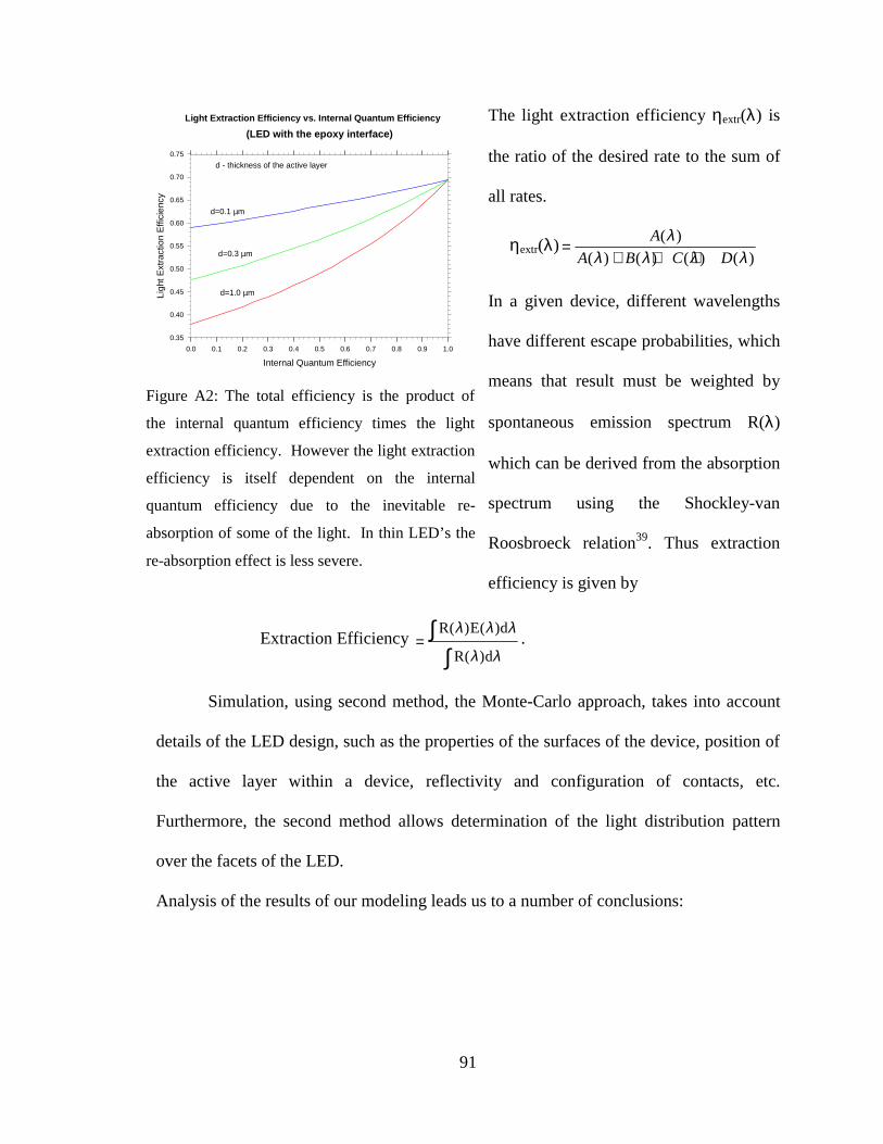
91
The light extraction efficiency ηextr(λ) is
the ratio of the desired rate to the sum of
all rates.
ηextr(λ) =+ + +
A
A B C D
( )
( ) ( ) ( ) ( )
λλ λ λ λ
In a given device, different wavelengths
have different escape probabilities, which
means that result must be weighted by
spontaneous emission spectrum R(λ)
which can be derived from the absorption
spectrum using the Shockley-van
Roosbroeck relation39. Thus extraction
efficiency is given by
Extraction Efficiency =∫
∫R E d
R d
( ) ( )
( )
λ λ λ
λ λ.
Simulation, using second method, the Monte-Carlo approach, takes into account
details of the LED design, such as the properties of the surfaces of the device, position of
the active layer within a device, reflectivity and configuration of contacts, etc.
Furthermore, the second method allows determination of the light distribution pattern
over the facets of the LED.
Analysis of the results of our modeling leads us to a number of conclusions:
Light Extraction Efficiency vs. Internal Quantum Efficiency
Internal Quantum Efficiency
0.0 0.1 0.2 0.3 0.4 0.5 0.6 0.7 0.8 0.9 1.0
Ligh
t Ext
ract
ion
Effi
cien
cy
0.35
0.40
0.45
0.50
0.55
0.60
0.65
0.70
0.75
d=1.0 µm
d=0.1 µm
d=0.3 µm
d - thickness of the active layer
(LED with the epoxy interface)
Figure A2: The total efficiency is the product of
the internal quantum efficiency times the light
extraction efficiency. However the light extraction
efficiency is itself dependent on the internal
quantum efficiency due to the inevitable re-
absorption of some of the light. In thin LED’s the
re-absorption effect is less severe.
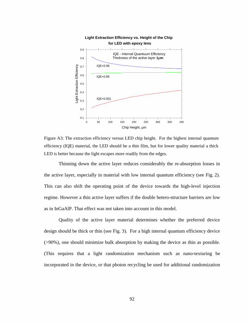
92
Thinning down the active layer reduces considerably the re-absorption losses in
the active layer, especially in material with low internal quantum efficiency (see Fig. 2).
This can also shift the operating point of the device towards the high-level injection
regime. However a thin active layer suffers if the double hetero-structure barriers are low
as in InGaAlP. That effect was not taken into account in this model.
Quality of the active layer material determines whether the preferred device
design should be thick or thin (see Fig. 3). For a high internal quantum efficiency device
(>90%), one should minimize bulk absorption by making the device as thin as possible.
(This requires that a light randomization mechanism such as nano-texturing be
incorporated in the device, or that photon recycling be used for additional randomization
Light Extraction Efficiency vs. Height of the Chip
Chip Height, µm
0 50 100 150 200 250 300 350 400
Ligh
t Ext
ract
ion
Effi
cien
cy
0.1
0.2
0.3
0.4
0.5
0.6
0.7
0.8
0.9
IQE - Internal Quantuum Efficiency
IQE=0.85
IQE=0.001
IQE=0.96
Thickness of the active layer 1µm
for LED with epoxy lens
Figure A3: The extraction efficiency versus LED chip height. For the highest internal quantum
efficiency (IQE) material, the LED should be a thin film, but for lower quality material a thick
LED is better because the light escapes more readily from the edges.
93
of light.). On the other hand, if the
active layer has a low (<90%)
internal efficiency, it’s better to
make a thick substrate device which
allows the photons to see the device
edges where four additional escape
cones are present. This increases the
photon to escape probability from
the semiconductor on the very first
surface bounce.
3. Monte-Carlo Simulations of light extraction efficiency
The photon gas model is a good
approximation when the average
photon path consists of many bounces
inside the LED. When low quality
contacts are introduced on the top and
bottom surfaces of the LED, a
comparison of the photon gas model
with the Monte-Carlo simulation
shows a difference (Fig. 4).
Nonetheless the qualitative scaling
Scaling Properties of Light Extraction Efficiency (air interface)
Chip Length, µm
0.00 0.01 0.02 0.03 0.04 0.05
Ligh
t Ext
ract
ion
Effi
cien
cy
0.0
0.1
0.2
0.3
0.4
0.5
0.6
0.7
0.8
0.9
1.0
Monte Carlo, 4 textured surfaces
Monte Carlo, 6 textured surfacesPhoton Gas Model
H=300µm;IQE=0.3
d=1um
R1=0.6, R2=0.5
Figure A4: Scaling properties of the light extraction
efficiency. When imperfect contacts are introduced
into the LED design, photon gas model gives
overestimated results for light extraction efficiency.
LED with one bottom contact
Position of the Active Layer
-H -3H/4 -H/2 -H/4 0 H/4 H/2 3H/4 H
Ligh
t Ext
ract
ion
Effi
cien
cy
0.40
0.42
0.44
0.46
0.48
0.50
0.52
0.54
0.56
0.58
0.60
0.62
0.64
0.66
0.68
0.70
R=0.3; QE=0.6
R=0.9; QE=0.6
Thickness of active layer - 0.1µm
Figure A5: Dependence of light extraction efficiency on
position of the active layer for a device with a sheet
bottom contact and a small circular top contact
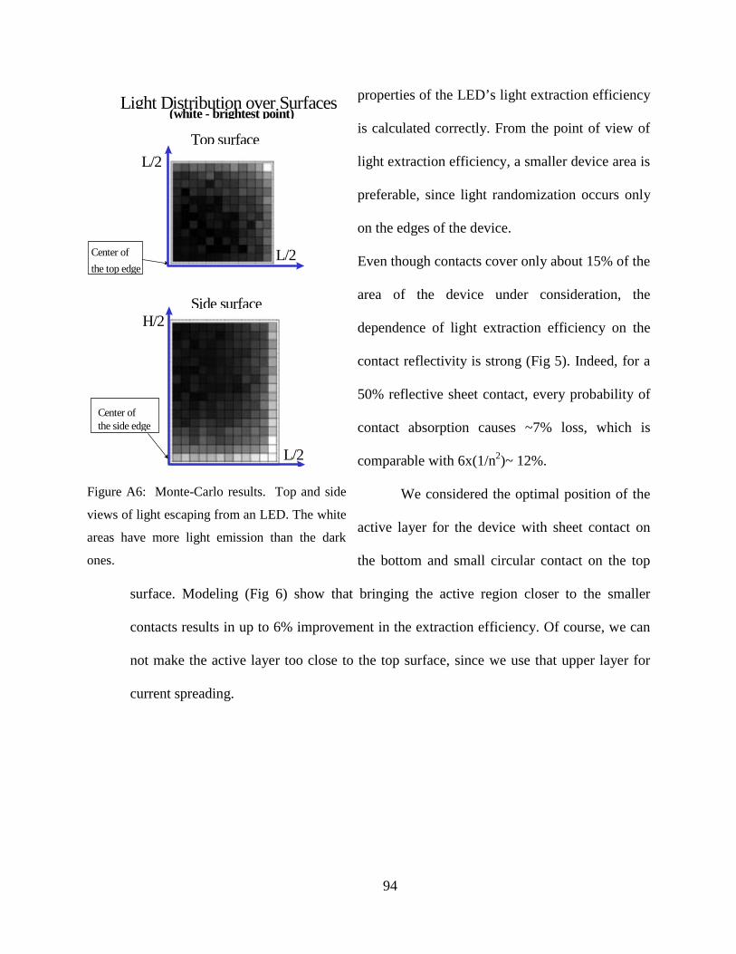
94
properties of the LED’s light extraction efficiency
is calculated correctly. From the point of view of
light extraction efficiency, a smaller device area is
preferable, since light randomization occurs only
on the edges of the device.
Even though contacts cover only about 15% of the
area of the device under consideration, the
dependence of light extraction efficiency on the
contact reflectivity is strong (Fig 5). Indeed, for a
50% reflective sheet contact, every probability of
contact absorption causes ~7% loss, which is
comparable with 6x(1/n2)~ 12%.
We considered the optimal position of the
active layer for the device with sheet contact on
the bottom and small circular contact on the top
surface. Modeling (Fig 6) show that bringing the active region closer to the smaller
contacts results in up to 6% improvement in the extraction efficiency. Of course, we can
not make the active layer too close to the top surface, since we use that upper layer for
current spreading.
Light Distribution over Surfaces
Top surface
(white - brightest point)
Side surface
Center of
the top edge
Center ofthe side edge
L/2
L/2
H/2
L/2
Figure A6: Monte-Carlo results. Top and side
views of light escaping from an LED. The white
areas have more light emission than the dark
ones.
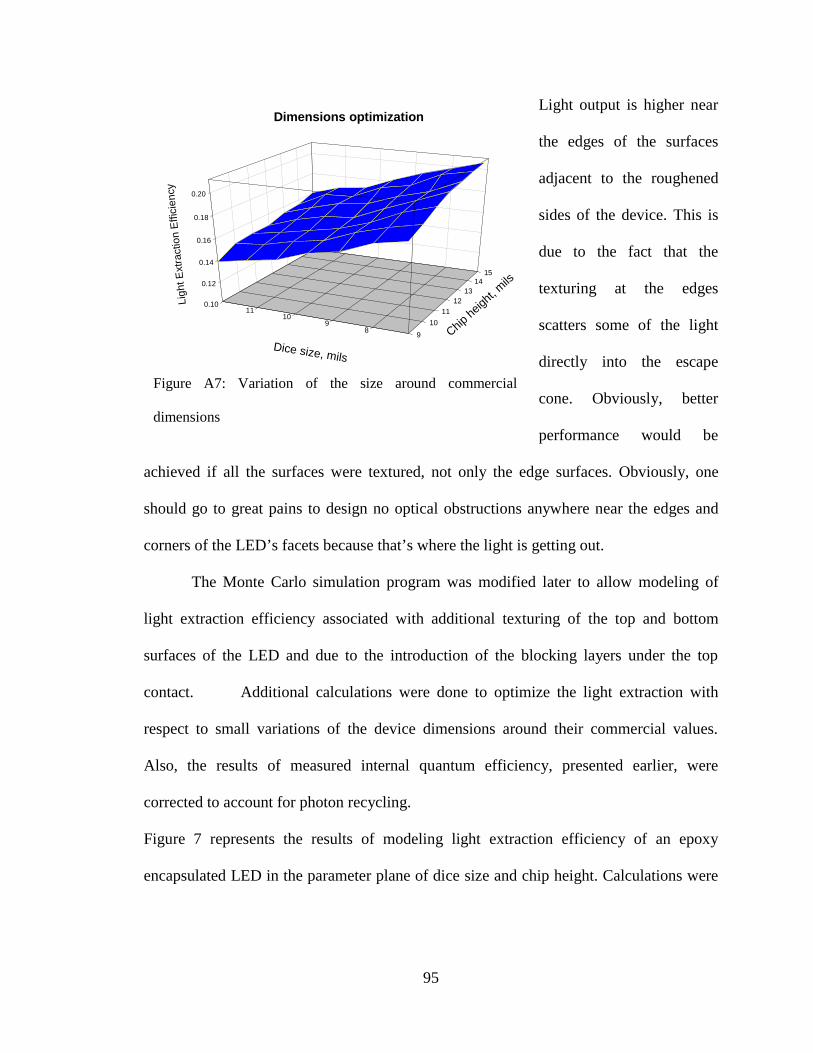
95
Light output is higher near
the edges of the surfaces
adjacent to the roughened
sides of the device. This is
due to the fact that the
texturing at the edges
scatters some of the light
directly into the escape
cone. Obviously, better
performance would be
achieved if all the surfaces were textured, not only the edge surfaces. Obviously, one
should go to great pains to design no optical obstructions anywhere near the edges and
corners of the LED’s facets because that’s where the light is getting out.
The Monte Carlo simulation program was modified later to allow modeling of
light extraction efficiency associated with additional texturing of the top and bottom
surfaces of the LED and due to the introduction of the blocking layers under the top
contact. Additional calculations were done to optimize the light extraction with
respect to small variations of the device dimensions around their commercial values.
Also, the results of measured internal quantum efficiency, presented earlier, were
corrected to account for photon recycling.
Figure 7 represents the results of modeling light extraction efficiency of an epoxy
encapsulated LED in the parameter plane of dice size and chip height. Calculations were
0.10
0.12
0.14
0.16
0.18
0.20
9
10
11
1213
1415
89
1011
Ligh
t Ext
ract
ion
Effi
cien
cy
Chip he
ight, m
ils
Dice size, mils
Dimensions optimization
Figure A7: Variation of the size around commercial
dimensions
96
done for an LED with internal quantum efficiency 0.7, with circular top contact of radius
55 microns and reflectivity 0.6 and sheet bottom contact with reflectivity 0.5. Bulk
absorption was taken to be 6
cm-1 and absorption in the
active layer was taken to be
104 cm-1. One can see that
light extraction efficiency
increases monotonically with
the height of the chip and
decreases with the length.
Figures 9a and 9b show the
effect of additional texturing
on the light extraction
efficiency. If light can be
scattered from the top and
bottom surfaces of the
device, it may significantly
increase escape probability
of photons. According to our
modeling, this texturing can
boost device efficiency by
10-15% of its initial value.
Scaling of light extraction efficiency
Height of the chip, mils
8 9 10 11 12 13 14 15 16
Ligh
t Ext
ract
ion
Effi
cien
cy
0.20
0.21
0.22
0.23
0.24
0.25
0.26
0.27
0.28
Only side surfaces are rough
Top and bottom surfaces textured
(a)
Scaling of light extraction efficiency
Dice size, mils
6 7 8 9 10 11 12 13
Ligh
t Ext
ract
ion
Effi
cien
cy
0.18
0.20
0.22
0.24
0.26
0.28
0.30
Only side surfaces are rough
Top and bottom surfaces textured
(b)
Figures A8(a,b) : Effect of additional texturing on
light extraction efficiency
97
Finally, we studied the possible change in LED performance due to incorporation of
current blocking layer under the top contact. However, modeling did not show any
significant improvement in the light extraction efficiency if blocking layers can absorb
light.
4. Conclusions
Light extraction efficiency of LED’s were calculated using photon gas model and Monte-
Carlo simulations. Recommendations were made to HP’s Opto-electrocnic division for
the design optimization, based on the results of the modeling.
98
Appendix B: Absorption Enhancement in Textured AlGaAs
Films for Solar Cells
Introduction:
We have studied light randomization and the absorption enhancement in textured ultra-
thin AlxGa1-xAs films, with a thickness corresponding to a few optical wavelengths. We
call this the “wave limit” of light trapping as opposed to the geometrical optics limit
that was studied before. A correlation between the degree of light randomization and
trapping, with the scale length of the texturization geometry was found. The observed
absorption enhancement corresponds to 90% randomization, or 90% of the best
possible theoretical value. A modified photon gas model is proposed to calculate the
light trapping and absorption at the band edge in the textured ultra-thin films.
It was proposed in late 1970s and early 1980’s that light trapping by total
internal reflection could be used to increase light absorption in semiconductor wafers.
Several techniques were developed, such as natural lithography40, metal islands41 and
anodical etch of the porous silicon42 to texturize thin silicon sheets for light trapping.
Yablonovitch34 showed, that in the low absorption limit, total randomization of the light
leads to the enhancement of absorption by the factor of 2nf2, where nf is film’s
refractive index. These results were confirmed experimentally by Deckman et al43 by
applying the natural lithography technique to amorphous silicon films. However, at the
moment there is no theory for angular dependence of light scattering from surfaces
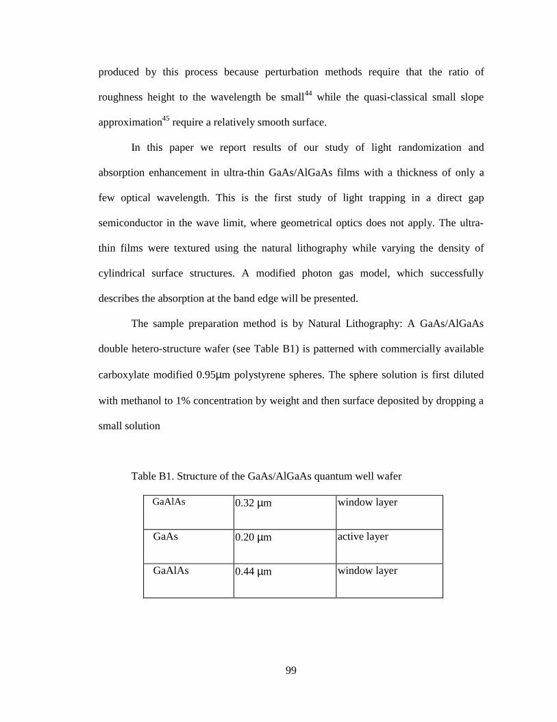
99
produced by this process because perturbation methods require that the ratio of
roughness height to the wavelength be small44 while the quasi-classical small slope
approximation45 require a relatively smooth surface.
In this paper we report results of our study of light randomization and
absorption enhancement in ultra-thin GaAs/AlGaAs films with a thickness of only a
few optical wavelength. This is the first study of light trapping in a direct gap
semiconductor in the wave limit, where geometrical optics does not apply. The ultra-
thin films were textured using the natural lithography while varying the density of
cylindrical surface structures. A modified photon gas model, which successfully
describes the absorption at the band edge will be presented.
The sample preparation method is by Natural Lithography: A GaAs/AlGaAs
double hetero-structure wafer (see Table B1) is patterned with commercially available
carboxylate modified 0.95µm polystyrene spheres. The sphere solution is first diluted
with methanol to 1% concentration by weight and then surface deposited by dropping a
small solution
Table B1. Structure of the GaAs/AlGaAs quantum well wafer
GaAlAs 0.32 µm window layer
GaAs 0.20 µm active layer
GaAlAs 0.44 µm window layer

100
AlAs 0.05 µm sacrificial layer
GaAs >100 µm substrate
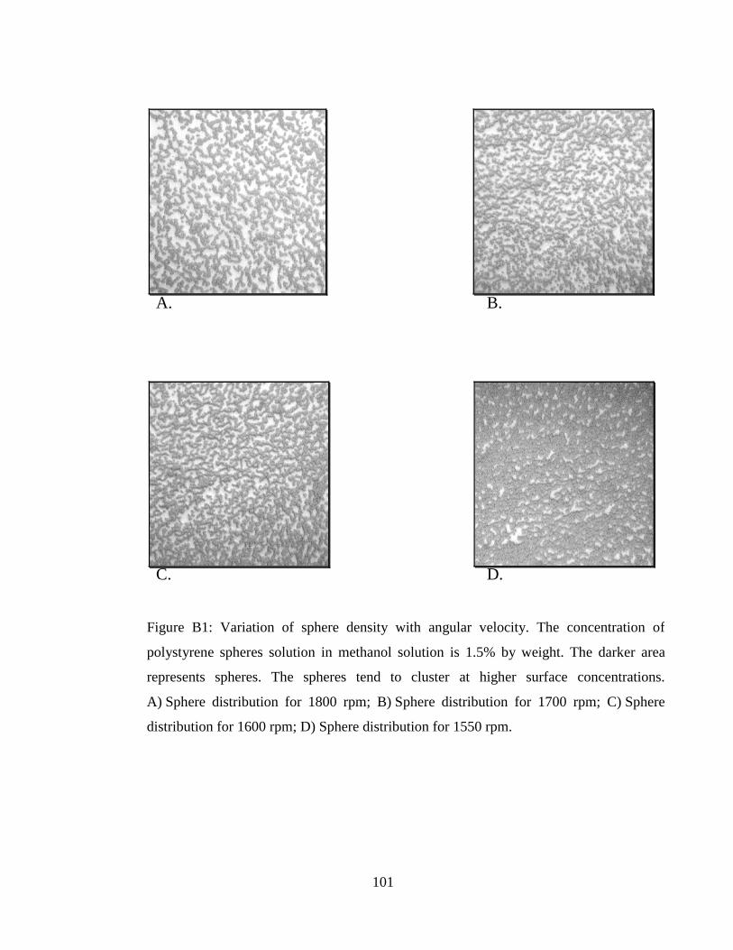
101
D.C.
A. B.
Figure B1: Variation of sphere density with angular velocity. The concentration of
polystyrene spheres solution in methanol solution is 1.5% by weight. The darker area
represents spheres. The spheres tend to cluster at higher surface concentrations.
A) Sphere distribution for 1800 rpm; B) Sphere distribution for 1700 rpm; C) Sphere
distribution for 1600 rpm; D) Sphere distribution for 1550 rpm.
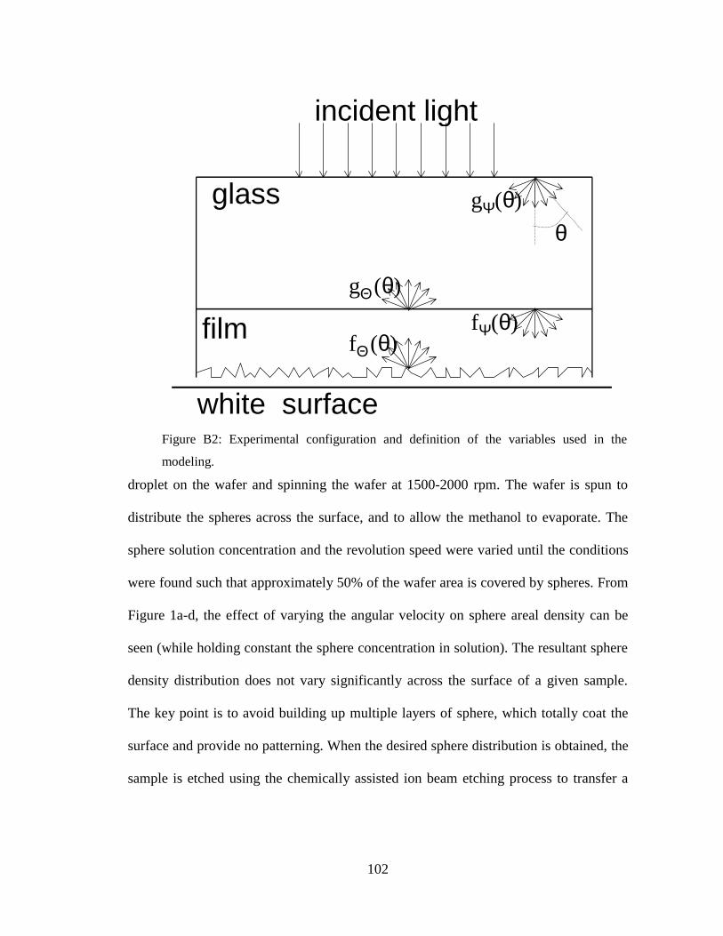
102
droplet on the wafer and spinning the wafer at 1500-2000 rpm. The wafer is spun to
distribute the spheres across the surface, and to allow the methanol to evaporate. The
sphere solution concentration and the revolution speed were varied until the conditions
were found such that approximately 50% of the wafer area is covered by spheres. From
Figure 1a-d, the effect of varying the angular velocity on sphere areal density can be
seen (while holding constant the sphere concentration in solution). The resultant sphere
density distribution does not vary significantly across the surface of a given sample.
The key point is to avoid building up multiple layers of sphere, which totally coat the
surface and provide no patterning. When the desired sphere distribution is obtained, the
sample is etched using the chemically assisted ion beam etching process to transfer a
glass
film
incident light
white surface
fΨ(θ)fΘ (θ)
gΘ (θ)
gΨ(θ)
θ
Figure B2: Experimental configuration and definition of the variables used in the
modeling.
103
pattern, using the spheres as a lithographic mask. In our work the transferred pattern
consists of 0.25µm high mesas, which is approximately 3/4 of the thickness of the top
AlGaAs layer. Following etching, the top three epitaxial layers (~1µm) of the wafer,
containing the active layer of the device, are removed from the substrate using the
epitaxial lift-off procedure (ELO)46. The wax supported sample is then bonded to a
glass slide with the untextured side against the glass by using a UV curable
polyurethane adhesive. The spectral reflectance, R(λ), of the textured and untextured
film was measured over a white surface using a standard integrating sphere setup. Then,
absorbance of the sample simply becomes:
A(λ)=1-R(λ), (1)
since there is no transmission outside of the sphere. Samples were held horizontally by
gravity so that no optically absorbing adhesive materials were necessary inside the
sphere. In all our measurements, the probe beam was incident on the glass side with the
semiconductor film on the rear, as shown in Figure 2. In this configuration specular
reflections from the glass-air and the semiconductor/glass interfaces were identical for
the textured and untextured samples. Thus, reflectivity at the front surface was
unchanged, since the texturing was at the rear surface. In all the textured samples,
an increase in absorption was measured in comparison with the untextured films (see
Figures 3&4). The maximum theoretical absorption, which can be attained is ≈80% due
to incident beam reflectivity from the glass/air (4%) and semiconductor/glass (16%)
interfaces. The best results were attained for samples, which were coated by
approximately 50% area coverage of polystyrene spheres and the corresponding
104
0.25µm high mesas. An absorbance increase from 45% up to ≈75% of a maximally
achievable result occurs for the sample in Figure 4 near the band edge. In our best
samples, the experimental value nearly reaches the maximum absorbance predicted by
theory, as can be seen in Figure 5. The absorbance oscillations, which occur for photon
energies above the bandgap, are due to Fabry-Perot fringes. The damping of these
Fabry-Perot oscillations in the textured film is an additional evidence of light
randomization produced through surface texturization. At energies below the bandgap,
free carrier absorption is enhanced from <1% up to the level of ≈20%. Unfortunately,
this produces heat rather then electron-hole pairs.We now describe the photon gas
model:
Consider a system consisting of the semiconductor film of thickness d with absorption
coefficient α and refractive index nf attached to a glass slide with the index of
refraction ng (as in Fig. 2 ). One surface of the film (opposite to the glass) is textured
and lies adjacent to the white reflecting surface so that incident monochromatic light
enters the film after passing through the glass slide. We assume that all photons which
reach the textured surface and white backing are scattered in all upward directions with
distribution function S(θ), where θ is the polar angle. If scattering is perfectly
Lambertian, S(θ)∝cosθ. Further, let us call f↑(θ) the flux density of photons in the film
near the textured surface, which are traveling up at angle θ. Due to symmetry, f↑
depends only on θ. Also, let f↓(θ) be a flux of photons in the film near the film/glass
interface, which are traveling down at angle θ. In the same manner, g↑(χ) and g↓(χ) are
defined as the photon flux densities in the glass at the film/glass interface going up and
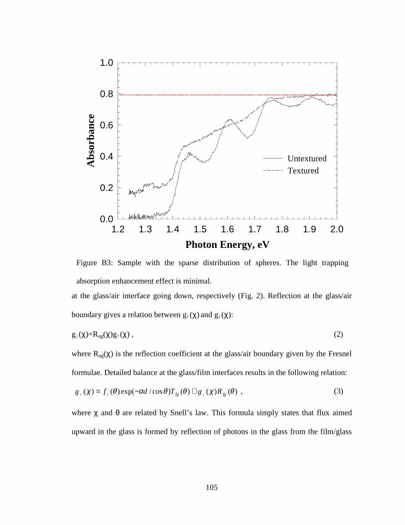
105
at the glass/air interface going down, respectively (Fig. 2). Reflection at the glass/air
boundary gives a relation between g↑(χ) and g↓(χ):
g↓(χ)=Rag(χ)g↑(χ) , (2)
where Rag(χ) is the reflection coefficient at the glass/air boundary given by the Fresnel
formulae. Detailed balance at the glass/film interfaces results in the following relation:
)()()()cos/exp()()( θχθθαθχ fgfg RgTdfg ↓↑↑ +−= , (3)
where χ and θ are related by Snell’s law. This formula simply states that flux aimed
upward in the glass is formed by reflection of photons in the glass from the film/glass
Photon Energy, eV
1.2 1.3 1.4 1.5 1.6 1.7 1.8 1.9 2.0
Abs
orba
nce
0.0
0.2
0.4
0.6
0.8
1.0
UntexturedTextured
Figure B3: Sample with the sparse distribution of spheres. The light trapping
absorption enhancement effect is minimal.
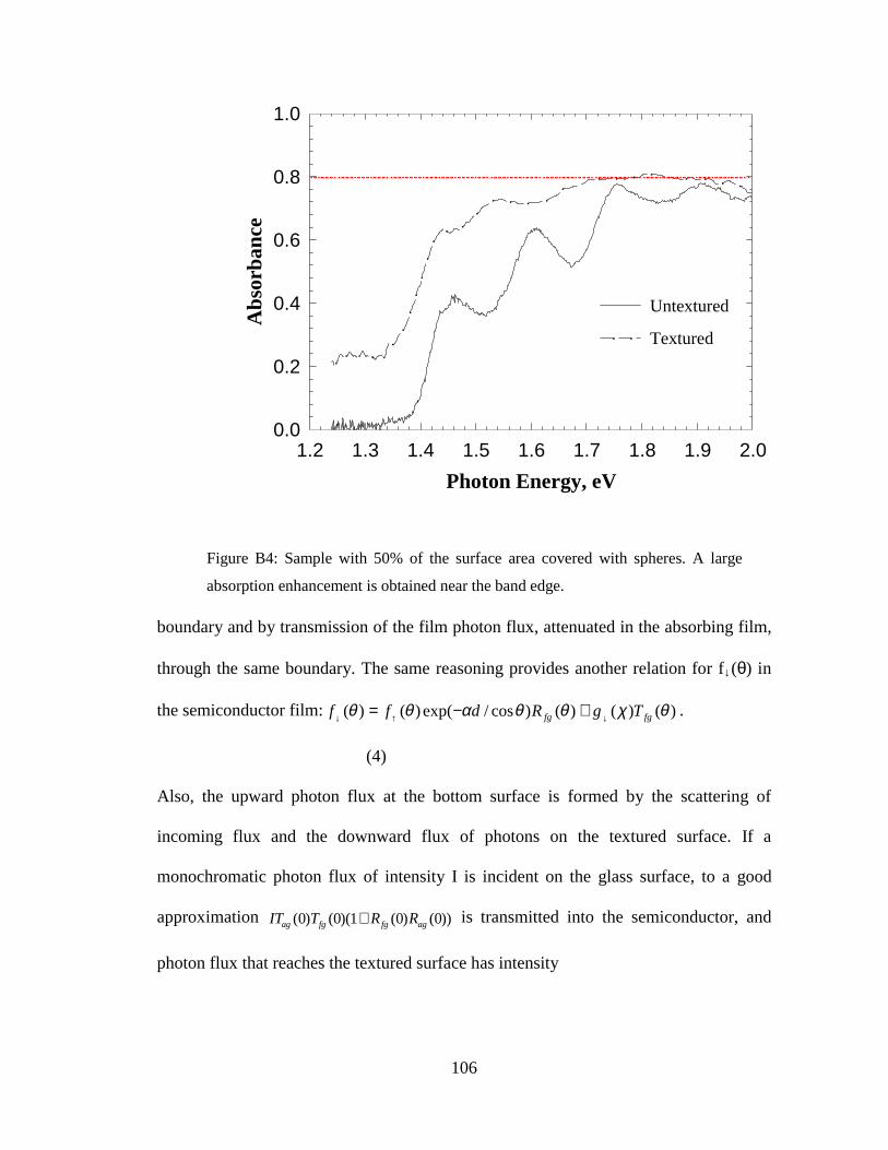
106
boundary and by transmission of the film photon flux, attenuated in the absorbing film,
through the same boundary. The same reasoning provides another relation for f↓(θ) in
the semiconductor film: )()()()cos/exp()()( θχθθαθθ fgfg TgRdff ↓↑↓ +−= .
(4)
Also, the upward photon flux at the bottom surface is formed by the scattering of
incoming flux and the downward flux of photons on the textured surface. If a
monochromatic photon flux of intensity I is incident on the glass surface, to a good
approximation IT T R Rag fg fg ag( ) ( )( ( ) ( ))0 0 1 0 0+ is transmitted into the semiconductor, and
photon flux that reaches the textured surface has intensity
Photon Energy, eV
1.2 1.3 1.4 1.5 1.6 1.7 1.8 1.9 2.0
Abs
orba
nce
0.0
0.2
0.4
0.6
0.8
1.0
Untextured
Textured
Figure B4: Sample with 50% of the surface area covered with spheres. A large
absorption enhancement is obtained near the band edge.
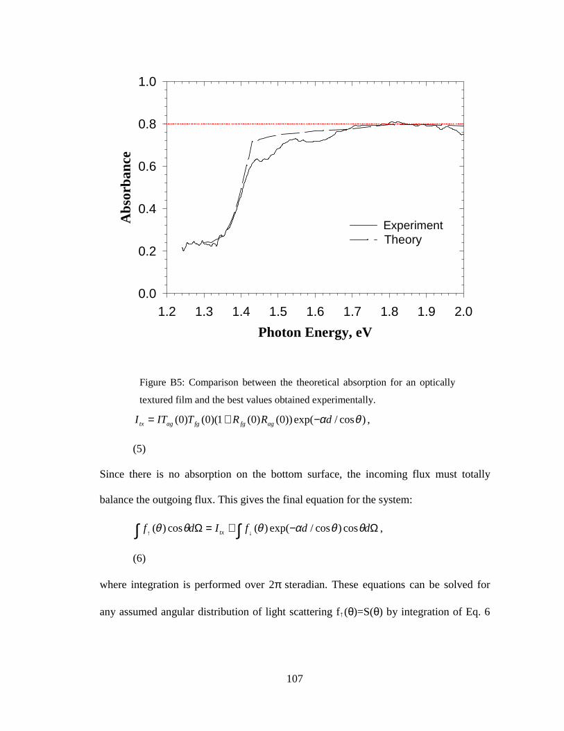
107
)cos/exp())0()0(1)(0()0( θαdRRTITI agfgfgagtx −+= ,
(5)
Since there is no absorption on the bottom surface, the incoming flux must totally
balance the outgoing flux. This gives the final equation for the system:
∫∫ Ω−+=Ω ↓↑ ddfIdf tx θθαθθθ cos)cos/exp()(cos)( ,
(6)
where integration is performed over 2π steradian. These equations can be solved for
any assumed angular distribution of light scattering f↑(θ)=S(θ) by integration of Eq. 6
Photon Energy, eV
1.2 1.3 1.4 1.5 1.6 1.7 1.8 1.9 2.0
Abs
orba
nce
0.0
0.2
0.4
0.6
0.8
1.0
ExperimentTheory
Figure B5: Comparison between the theoretical absorption for an optically
textured film and the best values obtained experimentally.
108
over the solid angles. In the photon gas model in the work of Deckman et al43, an
average Lambertian length for absorption is used. This is not valid for the strongly
nonlinear dependence of absorption on the propagation angle. Our theory, being more
general, explicitly takes into account absorption of photons scattered at different angles.
Instead of assumption of totally randomized photons, the model can deal with any
angular dependence of scattering, such as Lambertian in this paper. It can also
accommodate a dependence on incoming beam incidence angle. Instead of treating the
freestanding film, the sample is treated as bonded on the glass or sapphire slide, thus
taking into account a practical problem of the light trapping in the supporting slide.
Given this photon gas model, the amounts of reflected and absorbed light can be
calculated. Knowing the absorption spectrum of the film and its dispersion, one can
obtain the full spectral dependence of absorbance of the textured semiconductor film
bonded to a glass slide. Since the samples we studied contained various AlxGa1-xAs
alloy layers, the absorption coefficient α and the refractive index nf in the above
formulas are average values weighted by the thickness of the corresponding layers. The
calculated absorbance dependence for perfect Lambertian texturing is presented in
Figure 5 along with the experimental curve. Two curves show good agreement leading
us to believe that in the samples which have approximately 50% of the surface area
covered by 0.25µm high mesas at least 90% perfect light randomization has been
achieved.
We have studied light randomization and absorption in AlGaAs films textured by
means of natural lithography. A reproducible thin film fabrication process was
109
developed that provides 90% of ideally predicted band-edge absorption relative to our
theoretical model. Since the 1µm diameter spheres are visible in the optical microscope,
natural lithography with this sphere size is easy to monitor and optimize. Our technique
is applicable for fabrication of thin film solar cells and LED’s based on III-V
compounds. Epitaxial lift-off technology allows us to fabricate very thin AlGaAs solar
cells47, making them lighter and cheaper and providing higher operating point voltages.
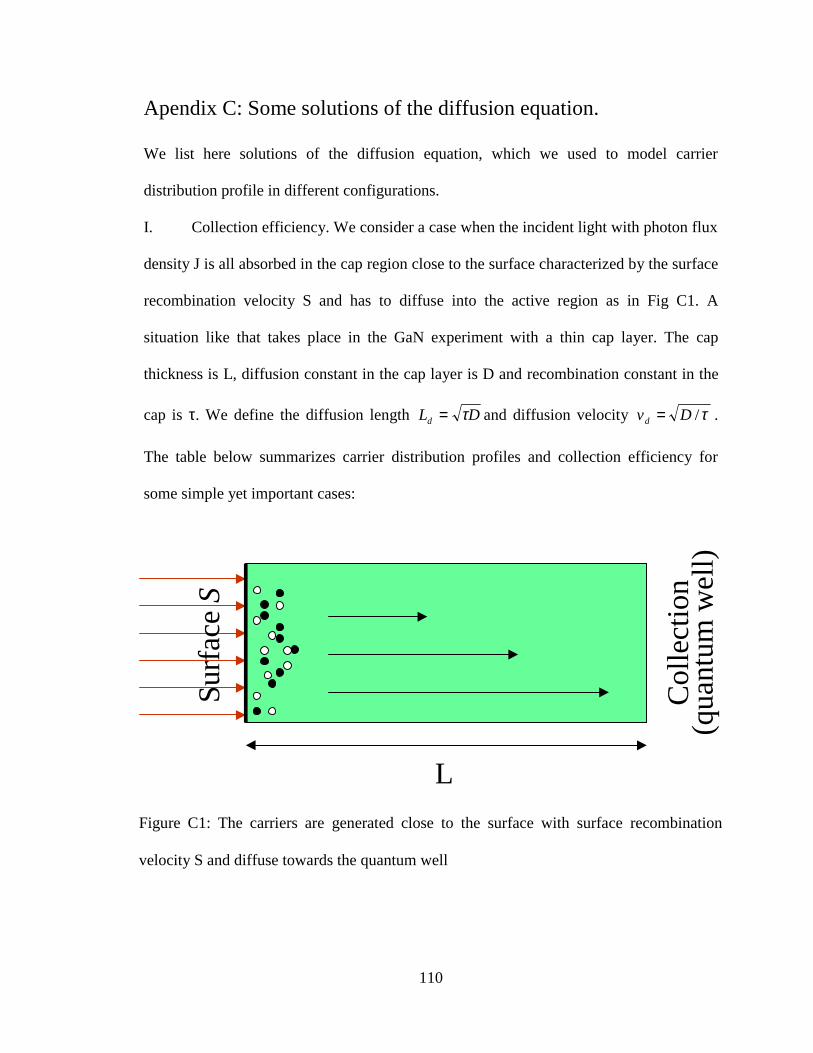
110
Apendix C: Some solutions of the diffusion equation.
We list here solutions of the diffusion equation, which we used to model carrier
distribution profile in different configurations.
I. Collection efficiency. We consider a case when the incident light with photon flux
density J is all absorbed in the cap region close to the surface characterized by the surface
recombination velocity S and has to diffuse into the active region as in Fig C1. A
situation like that takes place in the GaN experiment with a thin cap layer. The cap
thickness is L, diffusion constant in the cap layer is D and recombination constant in the
cap is τ. We define the diffusion length DLd τ= and diffusion velocity τ/Dvd = .
The table below summarizes carrier distribution profiles and collection efficiency for
some simple yet important cases:
Col
lect
ion
(qua
ntum
wel
l)
Sur
face
S
L
Figure C1: The carriers are generated close to the surface with surface recombination
velocity S and diffuse towards the quantum well
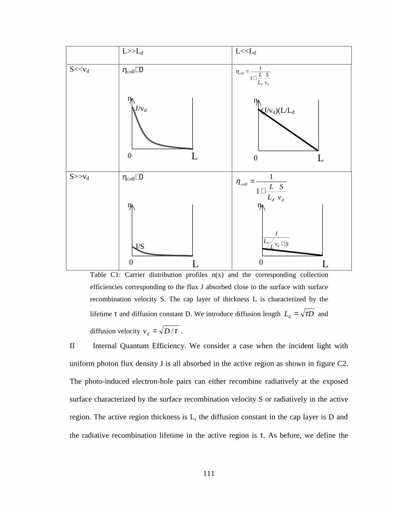
111
L>>Ld L<<Ld
S<<vd ηcoll∼0
dd
coll
v
S
L
L+=
1
1η
S>>vd ηcoll∼0
dd
coll
v
S
L
L+=
1
1η
Table C1: Carrier distribution profiles n(x) and the corresponding collection
efficiencies corresponding to the flux J absorbed close to the surface with surface
recombination velocity S. The cap layer of thickness L is characterized by the
lifetime τ and diffusion constant D. We introduce diffusion length DLd τ= and
diffusion velocity τ/Dvd = .
II Internal Quantum Efficiency. We consider a case when the incident light with
uniform photon flux density J is all absorbed in the active region as shown in figure C2.
The photo-induced electron-hole pairs can either recombine radiatively at the exposed
surface characterized by the surface recombination velocity S or radiatively in the active
region. The active region thickness is L, the diffusion constant in the cap layer is D and
the radiative recombination lifetime in the active region is τ. As before, we define the
n(J/vd)(L/Ld
0 L
n
SvLL
J
dd +
0 L
n
J/S
0 L
0
nJ/vd
L
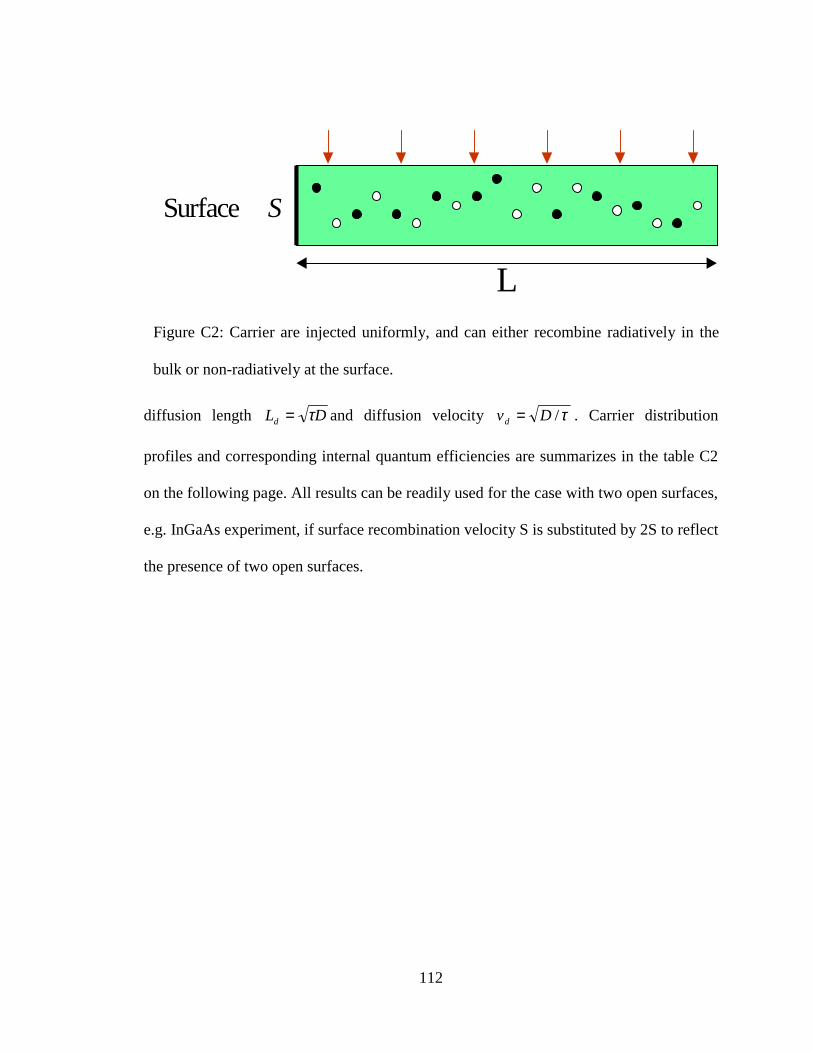
112
diffusion length DLd τ= and diffusion velocity τ/Dvd = . Carrier distribution
profiles and corresponding internal quantum efficiencies are summarizes in the table C2
on the following page. All results can be readily used for the case with two open surfaces,
e.g. InGaAs experiment, if surface recombination velocity S is substituted by 2S to reflect
the presence of two open surfaces.
Surface S
LFigure C2: Carrier are injected uniformly, and can either recombine radiatively in the
bulk or non-radiatively at the surface.
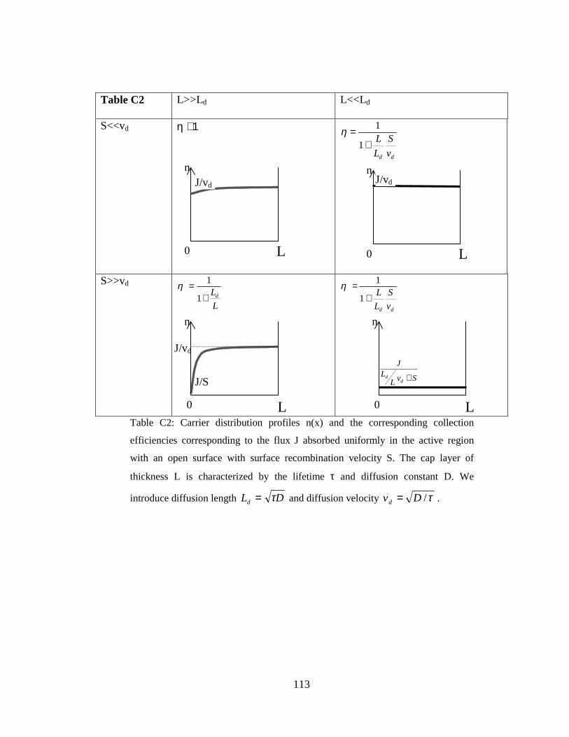
113
Table C2 L>>Ld L<<Ld
S<<vd η ∼1
dd v
S
L
L+=
1
1η
S>>vd
L
Ld+=
1
1η
dd v
S
L
L+=
1
1η
Table C2: Carrier distribution profiles n(x) and the corresponding collection
efficiencies corresponding to the flux J absorbed uniformly in the active region
with an open surface with surface recombination velocity S. The cap layer of
thickness L is characterized by the lifetime τ and diffusion constant D. We
introduce diffusion length DLd τ= and diffusion velocity τ/Dvd = .
n
0 L
n
SvLL
J
dd +
0 L
n
J/vd
0 L
0
nJ/vd
L
J/S
J/vd
114
References:
[1] P. Selenyi, Phys. Rev. 56, 477-480 (1939)
[2] R.G.Hulet, E.S. Hilfer, D. Kleppner, Phys. Rev. Lett, 59, 2955 (1955)
[3] E.M. Purcell, Phys. Rev. 69, 681(1946)
[4] P. Goy, J.M. Raimond, M. Gross, S. Haroche, Phys. Rev. Lett. 50, 1903 (1983)
[5] J. Gérard, B. Sermage, B. Gayral, B. Legrand, E. Costard, V. Tierry-Mieg,
“Enhanced spontaneous emission by quantum boxes in a monolithic optical microcavity,
”Phys. Rev. Lett., 1998, 91(5), pp. 1110-1113.
[6] E. Yablonovitch, ‘Inhibited spontaneous emission in solid-state physics and
electronics,’ Phys. Rev. Lett.,1987, 58 (20), pp. 2059-2062.
[7] Schubert, F., Wang, Y.-H., Cho, A.Y., Tu, L.-W., Zydzik, G.J.: ‘Resonant cavity
light-emitting diode,’ Appl. Phys. Lett., 1992, 60 (8), pp. 921-923.
[8] De Neve, H., Blondelle, J., Baets, R., Demeester, P., Van daele, P., Borghs, G.:
‘High efficiency planar microcavities LEDs’, International Conference on Physics of
Semiconductors (ICPS), July 1996, Berlin, Germany.
[9] P. Milonni, ‘The quantum vacuum: an introduction to quantum electrodynamics’
(Academic Press, Boston, 1994).
[10] E.M. Purcell, ’Spontaneous emission probabilities at radio frequencies,’ Phys.
Rev., 1946, 69, pp. 681-686.
115
[11] M. Boroditsky, R. Coccioli, E. Yablonovitch, ‘Analysis of photonic crystals for
light emitting diodes using the finite difference time domain technique,’ Photonics West
1998, January 28-29, 1998, San Jose, CA.
[12] J. Foresi, P. R. Villeneuve, J. Ferrera, E. R. Thoen, G. Steinmeyer, S. Fan,
J. D. Joannopoulos, L. C. Kimerling, H. I. Smith, E. P. Ippen, ‘Photonic-bandgap
microcavities in optical waveguides,’ Nature 390, 6656, pp.143-145 (1997).
[13] The mode volume given in [12] is twice as large due to a different definition. We
chose the definition in Eq. (26) as it agrees with the implicit definition given in Purcell,
Ref. 10.
[14] K. Sakoda, “Numerical study on localized defect modes in two-dimensional
triangular photonic crystals,” Journal of Appl. Phys., 1998, 84(3), pp. 1210-1214.
[15] O. Painter, J. Vuckovic, A. Scherer, “Defect modes of a two-dimensional
photonic rystal in a optically thin dielectric slab,” to be published in JOSA A.
[16] G. Mur, ‘Absorbing Boundary Conditions for the Finite-Difference approximation
of the time-domain electromagnetic-field equations,’ IEEE Trans. Eletromagnetic Comp.,
1991, 23 (4), pp. 377-382.
[17] S. Gedney, ‘An anisotropic perfectly matched layer-absorbing medium for the
truncation of FDTD-Lattices,’ IEEE Trans. Antennas Propagat., 1996, 44 (12), pp. 1630-
1639.
[18] J.-P. Berenger, ‘A perfectly matched layer for the absorption of electromagnetic
waves,’ J. Comp. Phys., 1994, 114 (2), pp.185-200.
116
[19] S.Fan, P.Villeneuve, J.Joannopoulos, E.F. Schubert,’ Phys. Rev. Lett., 1997, 78,
pp. 3295-3298.
[20] M. Boroditsky, E. Yablonovitch, "Photonic crystals boost light emission", Physics
World, 1997, 7, pp. 53-54.
[21] R. De Smedt, ‘Correction due to a finite permittivity for a ring resonator in free
space,’ IEEE Transactions on Microwave Theory and Techniques, 1984, MTT-32 , (10),
pp. 1288-1293.
[22] E. Yablonovitch, “Statistical Ray Optics”, J. Opt. Soc. Am 72(7), 1982, pp. 899-907
[23] H.R. Stuart, D.G. Hall, “Thermodynamic limit to light trapping in planar structures
J. Opt. Soc. Am A, 14(11), pp.3001-8.
[24] S. Keller, B. Keller, H. Maui, D. Kapolnek, A. Abare, U.Mishra, L. Coldren, and S.
DenBaars, International Symposium on Blue Lasers and Light Emitting Diodes, Chiba
University, Chiba, Japan, 1996
[25] C. Reese, M. Boroditsky, E. Yablonovitch, S. Keller, B.Keller, S. DenBaars,
“Absolute internal quantum efficiency of InGaN/GaN quantum wells”, 1996 CLEO
Conference, Technical Digest, Anaheim, California, p. 141.
[26] J.F. Muth, J.H. Lee, I..K. Shmagin, R.M. Kolbas, H.C. Casey, B,P .Keller,
U.K. Mishra, S.B. DenBaars, “Absorption coefficient, energy gap, exciton binding
energy, and recombination lifetime of GaN obtained from transmission measurements,”
Appl. Phys. Lett. 71, pp. 2572-2574 (1997); D. Brunner, H. Angerer, E. Brustarret,
F. Freudenberg, R. Hopler, R. dimitrov, O. Ambacher, M. Stutzmann, “Optical Constants
117
of epitaxial AlGaN films and their temperature dependence,” J. Appl. Phys., 82, pp5090-
96 (1997).
[27] I. Eliashevich, Y. Li, A. Osinsky, C. Tran, M. Brown, R. Karlicek, ”InGaN blue
light-emitting diodes with optimized n-GaN layer,” to be published in Proc. Photonics
West, Jan 23-29, 1999.
[28] E.Yablonovitch, T.J.Gmitter, R.Bhat, “Inhibited and enhanced spontaneous emission
from optically thin AlGaAs/GaAs double heterostructures,” Phys. Rev. Lett. 61(22),
pp. 2546-9 (1988).
[29] S.J.Pearton, F Ren; W.S.Hobson, C.R Abernathy; U.K. Chakrabarti, “Effects of wet
and dry etching and sulphide passivation on surface recombination velocities of InGaPp-
n junctions,” Proc. IEEE 6th International Conference on Indium Phosphide and Related
Materials, NewYork, USA: IEEE, 1994. p.186-9.
[30] M.Boroditsky, E.Yablonovitch, "Photonic crystals boost light emission", Physics
World No. 7, 1997 pp.53-54.
[31] A. J. Nelson and R. G. Sobers, J. Appl. Phys. 49, 6103 (1978).
[32] "Ultra-High Spontaneous Emission Quantum Efficiency, 99.7% Internally and 72%
Externally, From AlGaAs/GaAs/AlGaAs Double Heterostructures" I. Schnitzer,
E. Yablonovitch, C. Caneau, and T. J. Gmitter, Appl. Phys. Lett. 62, 131 (1993).
[33] W. N. Carr and G. E. Pittman, Appl. Phys. Lett. 3, 173 (1963).
[34] E. Yablonovitch, J. Opt. Soc. Am. 72, 899 (1982). E. Yablonovitch and G. D. Cody,
IEEE Trans. Elec. Dev. ED-29, 300 (1982).
118
[35] M. Green, M. Garcia-Parajo, F. Khaleque, and R. Murray, Appl. Phys. Lett. 62, 264
(1993).
[36] W. B. Joyce, R. Z. Bachrach, R. W. Dixon, and D. A. Sealer, J. Appl. Phys. 45, 2229
(1974).
[37] I. Schnitzer, E. Yablonovitch, C. Caneau, T.J Gmitter, J.Appl. Phys. Lett. 62, 131
(1993).
[38] “Very High-Efficiency Semiconductor Wafer-Bonded Transparent Substrate
(AlGa)InP/GaP Light-Emitting Diodes”, F. A. Kish, F. M. Steranka, D. C. DeFevere, D.
A. Vanderwater, K. G. Park, C. P. Kuo, T. D. Osentowski, M. J. Peanasky, J. G. Yu, R.
M. Fletcher, D. A. Steigerwald, M. G. Craford, and V. M. Robbins, Appl. Phys. Lett. 64,
2839 (1994).
[39] J. Pankove “Optical processes in semiconductors”, Dover Publications, New York,
1975.
[40] Deckman, J.N. Dunsmuir, “Natural lithography,” Appl. Phys. Lett 41, 377-379
(1982)
[41] H.Stewart, D. Hall, “Absorption enhancement in silicon-on-insulator waveguides
using metal island films,” Appl. Phys. Lett 69, 2327-29 (1996)
[42] A. Krotcus. V. Pacebutas, J. Kavaliauskas, I. Subacius, K. Grigoras, I. Simkiene,
“Light trapping effect in silicon wafers with anodically etched surfaces”, Applied physics
A, 64, pp.357-60, Springer-Vesrlag, April 1997.
119
[43] H.W.Deckman, C.R.Wronsky, H.Witzke, E.Yablonovitch, “Optically enhanced
amourphous silicon solar cells,” Appl. Phys. Lett. 42, 968-970(1982),
[44] P.M. van den Berg, T.J.Fokkema, “The Rayleigh hypothesis in the theory of
reflection by a grating,” J.Opt.Soc.Am. 69,27-31(1979).
[45] A.G.Voronovitch, Sov. “Small slope approximation in wave scattering by rough
surfaces”, Sov. Phys. JETP 62, 65-70(1985).
[46] E. Yablonovitch, R. Gmitter, J.P.Haribson, R.Bhat “Extreme selectivity in the
epitaxial lift-off GaAs films“, Appl. Phys. Lett. 51, 2222-24(1987).
[47] X.Y.Lee, A.K.Verma, C.Q.Wu, M.Goertemiller, E.Yablonovitch, ”Thin film GaAs
solar cells on glass substrates by epitaxial lift-off”, Procedings of 25th PVSC, May 13-17
1996, Washington D.C., pp.53-55.