Embed Size (px)
Citation preview
EECS150 Fall 2007 Checkpoint 2
UNIVERSITY OF CALIFORNIA AT BERKELEYCOLLEGE OF ENGINEERING
DEPARTMENT OF ELECTRICAL ENGINEERING AND COMPUTER SCIENCE
Checkpoint 2Video Encoder and Basic User Interface
1.0 MotivationThe goal of this semester’s project is to build an interactive audio conferencing
system. In order to do that, you will need to develop modules that allow us to not only see, but also interact with the conferencing system beyond the LEDs and buttons available on the FPGA.
In this checkpoint, you will build the modules that determine the “look and feel” of the project. It is divided into three milestones:
1. A video encoder module that uses the NTSC (TV) standard to communicate with the LCD monitors hooked up to each station.
2. A video display module that determines the video data to be read by the video encoder, with the ability to display ASCII text.
3. A user interface module that uses button presses from a Nintendo 64 game controller to interact with the video display module.
Keep in mind that you will be using these modules in future checkpoints, so be sure to design your Verilog ahead of time, comment you code and test everything thoroughly. Because you will be keeping and relying on this code for months, it will actually save you many stressful hours to ensure it works well now, rather than when you are about to finish the project.
Many of you will be at least reasonably familiar with video as it is used on computer systems, with standard VGA or DVI interfaces, complicated video cards and high-resolution data grade CRT or LCD monitors. In this checkpoint you will be introduced to the far older and more universal world of broadcast video. You will be working with NTSC standard video, as used in the U.S. broadcast TV industry, and in fact on your TV at home.
NTSC is a reasonably simple standard, which is widely used and readily available. But one of the primary reasons to use it is that despite advances such as DVI and HDTV, the video standards we will be using (which have survived from the invention of black-and-white television) will continue to affect video for a long time to come.
“BECAUSE YOU WILL BE KEEPING AND RELYING ON THIS CODE FOR MONTHS, IT WILL ACTUALLY SAVE YOU MANY STRESSFUL HOURS TO ENSURE IT WORKS WELL NOW, RATHER THAN WHEN YOU ARE ABOUT TO FINISH THE PROJECT”
2.0 IntroductionThe video encoder module you will building for this checkpoint is a simple
protocol bridge, connecting a memory structure, in this case a simple ROM-like module,
UCB 1 2007
EECS150 Fall 2007 Checkpoint 2
to a byte wide video data stream. In the second phase of the phase of the project, you will replace the given ROM-like module with a module of your own that displays video data that you define.
The primary responsibilities of the video encoder are:1. Request the video data to be transmitted
a. Must track which line and pixel is being sent when2. Generate video framing signals
a. Start-of-active-video and end-of-active-video (SAV and EAV) signals to delineate row boundaries
b. Blanking and field control to indicate what type of data will be sentc. Black data to fill blanking periods
3. Clip the video data to the allowable value rangea. Data values less than 0x10 or more than 0xF0 must be clipped
4. Initialize and control the Analog Devices ADV7194 hardwarea. The ADV7194 is a digital-to-analog converter which generates
analog video signalsb. Use I2C to initialize the ADV7194 to the proper mode
The video encoder will be responsible for abstracting away all the complexities of dealing with the ADV7194 and properly framing the data, leaving only the task of supplying valid video data, which for the first phase will be provided by a simple ROM-like module to generate a test pattern of solid color bars.
2.1 ITU-R BT.601 VideoWhen television broadcasts were slated to move from black-and-white to color,
there was a significant concern over the existing investments in black-and-white sets. Not only were engineers concerned that old TV sets would be unable to receive newer signals, making old equipment useless, but they were worried that signals from older stations would not be received by the new color sets, preventing the adoption and sales of color TVs. As such a compromise was made resulting in the color scheme outlined below.
2.1.1 RGB Coloring & Human PerceptionThe standard color scheme used when dealing with light, as we are in video
applications, is based on the three primary colors: Red, Green and Blue.Human eyes have two sets of photoreceptors which detect incoming light:
Rods cannot detect color, but they are very sensitive to brightness Cones can detect color, but they are significantly less sensitive
The primary colors Red, Green and Blue derive from the fact that cones come in three colors: Red, Green and Blue. This means that rather than generating any possible color, it is enough to be able to mix varying proportions of Red, Green and Blue, as our eyes perceive every other color in terms of the RGB proportions in them.
Just as important is the relative sensitivity of the rods and cones in our eyes, for example, because cones are not particularly sensitive, it is more than sufficient to store 8bits of intensity for each color in RGB, leading to the widespread use of 24bit color.
UCB 2 2007
EECS150 Fall 2007 Checkpoint 2
Less known but even more important is the fact that the rods in our eyes, which are sensitive only to brightness, are much more sensitive. This means that while we can easily perceive slight differences in brightness using our cones, it is more difficult to perceive subtle shades of color.
2.1.2 YUV ColoringAs a result of the economic pressures to maintain compatibility between older
black and white TVs and the newer color models, as well as the way in which humans perceive light, engineers designed a video format which would transmit intensity, or luminance, and color, or chrominance, separately.
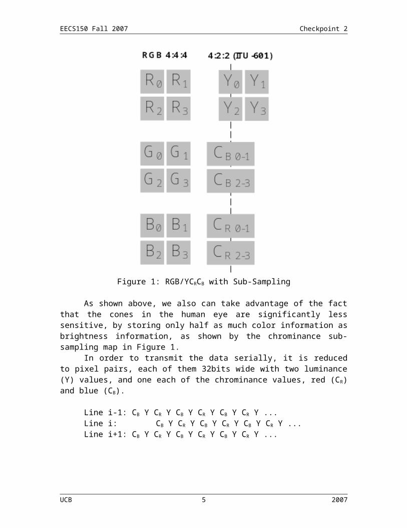
This means that instead of storing the Red, Green and Blue content of a pixel in our video, we will store its luminance (Y) or brightness and its red (CR/V) and blue (CB/U) chrominance, or color.
Figure 1: RGB/YCRCB with Sub-Sampling
As shown above, we also can take advantage of the fact that the cones in the human eye are significantly less sensitive, by storing only half as much color information as brightness information, as shown by the chrominance sub-sampling map in Figure 1.
In order to transmit the data serially, it is reduced to pixel pairs, each of them 32bits wide with two luminance (Y) values, and one each of the chrominance values, red (CR) and blue (CB).
UCB 3 2007
EECS150 Fall 2007 Checkpoint 2
Line i-1: CB Y CR Y CB Y CR Y CB Y CR Y ...Line i: CB Y CR Y CB Y CR Y CB Y CR Y ...Line i+1: CB Y CR Y CB Y CR Y CB Y CR Y ...
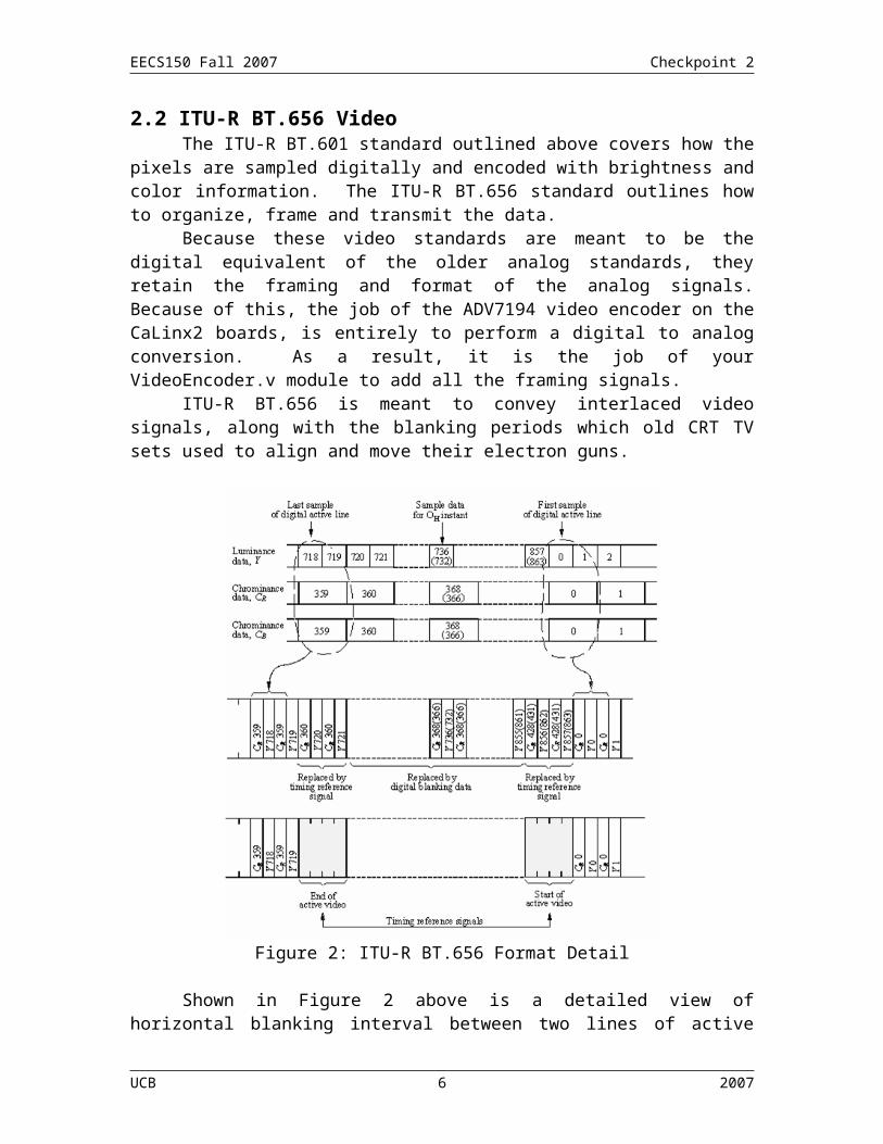
2.2 ITU-R BT.656 VideoThe ITU-R BT.601 standard outlined above covers how the pixels are sampled
digitally and encoded with brightness and color information. The ITU-R BT.656 standard outlines how to organize, frame and transmit the data.
Because these video standards are meant to be the digital equivalent of the older analog standards, they retain the framing and format of the analog signals. Because of this, the job of the ADV7194 video encoder on the CaLinx2 boards, is entirely to perform a digital to analog conversion. As a result, it is the job of your VideoEncoder.v module to add all the framing signals.
ITU-R BT.656 is meant to convey interlaced video signals, along with the blanking periods which old CRT TV sets used to align and move their electron guns.
Figure 2: ITU-R BT.656 Format Detail
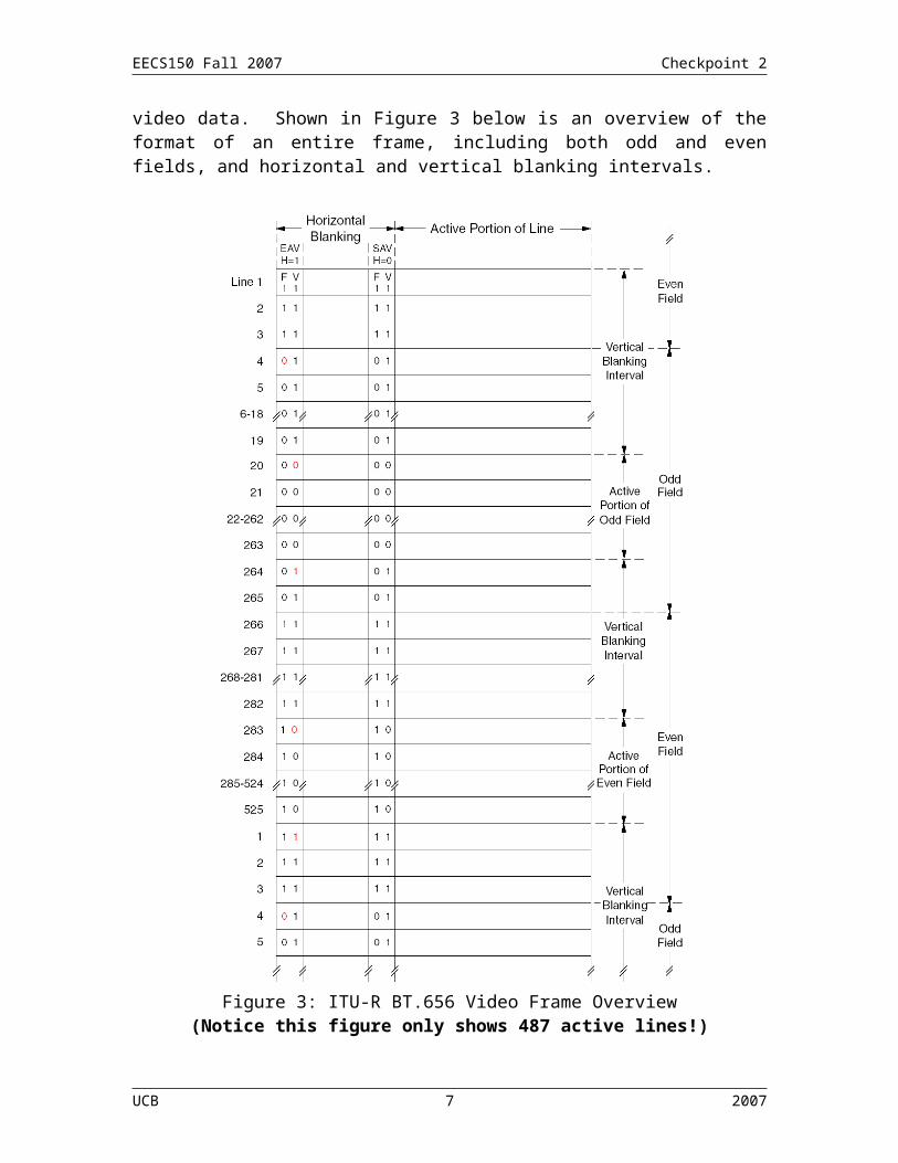
Shown in Figure 2 above is a detailed view of horizontal blanking interval between two lines of active video data. Shown in Figure 3 below is an overview of the format of an entire frame, including both odd and even fields, and horizontal and vertical blanking intervals.
UCB 4 2007
EECS150 Fall 2007 Checkpoint 2
Figure 3: ITU-R BT.656 Video Frame Overview(Notice this figure only shows 487 active lines!)
ITU-R BT.656 Video is essentially a stream of lines of video, as shown in Figure 3 above. Each line begins with an EAV (counter intuitively), followed by a horizontal blanking interval, followed by an SAV and then, if the line is not in a vertical blanking interval 720 pixels (1440 bytes) of active video data.
UCB 5 2007
EECS150 Fall 2007 Checkpoint 2
The EAV and SAV codes are detailed in the Video in a Nutshell document on the EECS150 website. Please refer to that or the lab lecture for more details.
3.0 PrelabPlease make sure to complete the prelab before you attend your lab section. You
will not be able to finish this checkpoint in 3hrs!1. Read this handout thoroughly.
a. Pay particular attention to section 4.0 Lab Procedure as it describes what you will be doing in detail.
2. Examine the documents page of the websitea. You will need to get used to reading datasheets, like these.
They form the core of information available to hardware designers.
b. http://www-inst.eecs.berkeley.edu/~cs150/fa04/ Documents.htm#Video
c. Read the ADV7194 Datasheetd. Read Video in a Nutshell by Tom Oberheime. Read the ITU-R BT.656 Standardf. Read the ITU-R BT.601 Standard
3. Examine the Verilog provided for this checkpointa. There isn’t much, so it should be pretty clearb. You do not need to understand the I2C module in full detail
4. Start your design ahead of time.a. Begin with schematics and bubble-and-arc diagramsb. Come prepared for your design reviewc. VideoEncoder.v will require significant debugging to finish.
Make sure to write at least a draft of it ahead of time.d. Start building your testbench early
i. Perhaps have one person design the module and the other design the testbench
5. You will need at least the entire 3hr lab!a. You will need to test and debug your verilog thoroughly.b. You must build a reliable interface with a real hardware
component!
4.0 Lab ProcedureRemember to manage your Verilog, projects and folders well. Doing a poor
job of managing your files can cost you hours of rewriting code, if you accidentally delete your files.
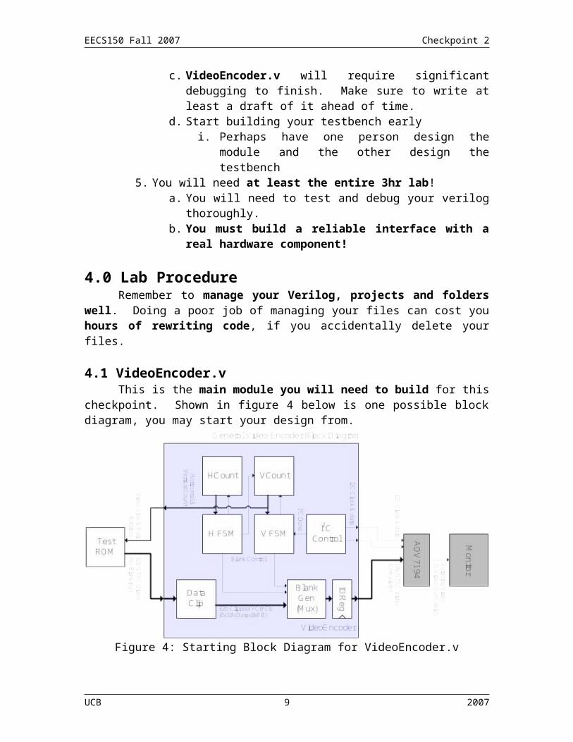
4.1 VideoEncoder.vThis is the main module you will need to build for this checkpoint. Shown in
figure 4 below is one possible block diagram, you may start your design from.
UCB 6 2007
EECS150 Fall 2007 Checkpoint 2
Figure 4: Starting Block Diagram for VideoEncoder.v
The essential functions of you module are listed in section 2.0 Introduction, above. Note that out of this list, we have provided you with the I2C interface, in an effort to keep the checkpoint manageable. The primary reason for this is that if the ADV7194 chip is improperly initialized, you will not see ANY video on the board, making debugging rather difficult.
Shown in Table 1 below is the port specification list for VideoEncoder.v.
Signal Width Dir DescriptionVE_P 10 O Outgoing NTSC Video (Use {Data, 2’b00})VE_SCLK 1 O I2C Clock (For Initialization)VE_SDA 1 O I2C Data (For Initialization)VE_PAL_NTSC 1 O PAL/NTSC Mode Select (Always 1’b0)VE_RESET_B_ 1 O Active low reset out the ADV7194VE_HSYNC_B_ 1 O Manual sync control (Always 1’b1)VE_VSYNC_B_ 1 O Manual sync control (Always 1’b1)VE_BLANK_B_ 1 O Manual sync control (Always 1’b1)VE_SCRESET 1 O Manual sync control (Always 1’b0)VE_CLKIN 1 O Clock (27MHz, Clock Signal)Clock 1 I The Clock signalReset 1 I Reset all counters and registers (Not necessarily
to 0)Din 32 I Requested video data YCRYCB
InRequest 1 O Request signal, should be high for one out four cycles during active video periods. DIn will be valid after the riding edge where this is 1’b1.
InRequestLine 9 O The line from which you are requesting video data, (Use {Line, Field})
UCB 7 2007
EECS150 Fall 2007 Checkpoint 2
InRequestPair 9 O The pair of pixels which you are requesting from the video ROM. Notice that this address should go up by one for each 4-byte pixel pair.
Table 1: Port Specification for VideoEncoder.v
During the blanking interval, you should fill the video data with black (Luma 0x10, Chroma 0x80)
It is not necessary to start transmitting an EAV immediately when the I2C interface is done, as indicated by the I2CDone signal.
o The ADV7194 will wait until it gets an EAV (0xFF, 0x00, 0x00, code) before it begins decoding your data.
Once you do begin sending, there is a very tight constraint on what you send on which cycle, check your counters carefully as even a small mistake may cause major problems.
o A shaky or scrolling picture most likely means one of your many counters is off by a few cycles. Check your state machine/counter logic.
o You may wish to design your testbench to count cycles too, in an effort to automatically double check your work.
Weird colors most likely mean that you are transmitting the Y, CR and CB values in the wrong order.
o Lots of green and purple means you have swapped the luma and chroma values.
o Wrong values of Y,Cb and Cr could also result in the monitor losing sync, make sure to clip all actual video data to the range 0x10 – 0xF0.
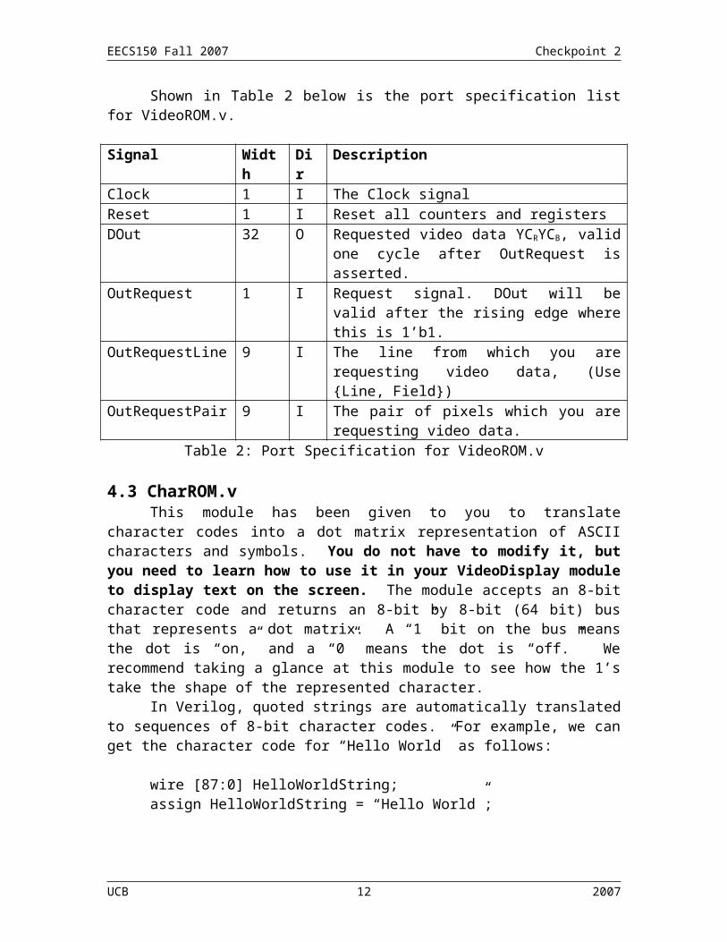
4.2 VideoROM.vWe have given you this ROM-like module to test the video encoder. You do not
have to modify it. It has a very simple interface that provides video data to the encoder based on the requested coordinates. We suggest looking at this module to find out how to divide the screen into sections – it will help you get started on VideoDisplay.v.
Shown in Table 2 below is the port specification list for VideoROM.v.
Signal Width Dir DescriptionClock 1 I The Clock signalReset 1 I Reset all counters and registersDOut 32 O Requested video data YCRYCB, valid one cycle
after OutRequest is asserted.OutRequest 1 I Request signal. DOut will be valid after the rising
edge where this is 1’b1.OutRequestLine 9 I The line from which you are requesting video
data, (Use {Line, Field})OutRequestPair 9 I The pair of pixels which you are requesting video
data.
UCB 8 2007
EECS150 Fall 2007 Checkpoint 2
Table 2: Port Specification for VideoROM.v
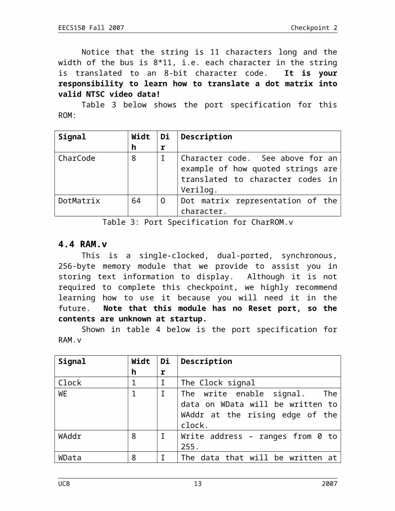
4.3 CharROM.vThis module has been given to you to translate character codes into a dot matrix
representation of ASCII characters and symbols. You do not have to modify it, but you need to learn how to use it in your VideoDisplay module to display text on the screen. The module accepts an 8-bit character code and returns an 8-bit by 8-bit (64 bit) bus that represents a dot matrix. A “1” bit on the bus means the dot is “on,” and a “0” means the dot is “off.” We recommend taking a glance at this module to see how the 1’s take the shape of the represented character.
In Verilog, quoted strings are automatically translated to sequences of 8-bit character codes. For example, we can get the character code for “Hello World” as follows:
wire [87:0] HelloWorldString;assign HelloWorldString = “Hello World”;
Notice that the string is 11 characters long and the width of the bus is 8*11, i.e. each character in the string is translated to an 8-bit character code. It is your responsibility to learn how to translate a dot matrix into valid NTSC video data!
Table 3 below shows the port specification for this ROM:
Signal Width Dir DescriptionCharCode 8 I Character code. See above for an example of how
quoted strings are translated to character codes in Verilog.
DotMatrix 64 O Dot matrix representation of the character.Table 3: Port Specification for CharROM.v
4.4 RAM.vThis is a single-clocked, dual-ported, synchronous, 256-byte memory module that
we provide to assist you in storing text information to display. Although it is not required to complete this checkpoint, we highly recommend learning how to use it because you will need it in the future. Note that this module has no Reset port, so the contents are unknown at startup.
Shown in table 4 below is the port specification for RAM.v
Signal Width Dir DescriptionClock 1 I The Clock signalWE 1 I The write enable signal. The data on WData will
be written to WAddr at the rising edge of the clock.
WAddr 8 I Write address – ranges from 0 to 255.WData 8 I The data that will be written at the positive edge
of the clock when WE is 1’b1.
UCB 9 2007
EECS150 Fall 2007 Checkpoint 2
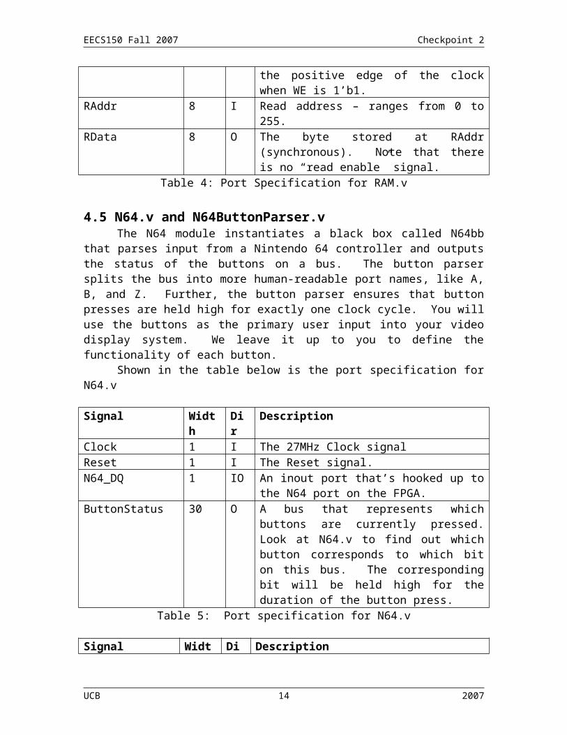
RAddr 8 I Read address – ranges from 0 to 255.RData 8 O The byte stored at RAddr (synchronous). Note
that there is no “read enable” signal.Table 4: Port Specification for RAM.v
4.5 N64.v and N64ButtonParser.vThe N64 module instantiates a black box called N64bb that parses input from a
Nintendo 64 controller and outputs the status of the buttons on a bus. The button parser splits the bus into more human-readable port names, like A, B, and Z. Further, the button parser ensures that button presses are held high for exactly one clock cycle. You will use the buttons as the primary user input into your video display system. We leave it up to you to define the functionality of each button.
Shown in the table below is the port specification for N64.v
Signal Width Dir DescriptionClock 1 I The 27MHz Clock signalReset 1 I The Reset signal.N64_DQ 1 IO An inout port that’s hooked up to the N64 port on
the FPGA.ButtonStatus 30 O A bus that represents which buttons are currently
pressed. Look at N64.v to find out which button corresponds to which bit on this bus. The corresponding bit will be held high for the duration of the button press.
Table 5: Port specification for N64.v
Signal Width Dir DescriptionClock 1 I The 27Mhz Clock signalReset 1 I The Reset signal.ButtonStatus 30 I From output of N64.vA 1 O A button pressed (high for 1 cycle)B 1 O B button pressed (high for 1 cycle)Z 1 O Z button pressed (high for 1 cycle)Start 1 O Start button pressed (high for 1 cycle)DU 1 O D-pad Up button pressed (high for 1 cycle)DD 1 O D-pad Down button pressed (high for 1 cycle)DL 1 O D-pad Left button pressed (high for 1 cycle)DR 1 O D-pad Right button pressed (high for 1 cycle)L 1 I L button pressed (high for 1 cycle)R 1 I R button pressed (high for 1 cycle)CU 1 I C-Up button pressed (high for 1 cycle)CD 1 O C-Down button pressed (high for 1 cycle)CL 1 O C-Left button pressed (high for 1 cycle)CR 1 O C-Right button pressed (high for 1 cycle)Joystick 16 O Analog Joystick
UCB 10 2007
EECS150 Fall 2007 Checkpoint 2
[15:8] – Left/Center/Right (-/0/+) [7:0] – Up/Center/Down (+/0/-)
Table 6: Port Specification for N64ButtonParser.v
4.6 UserInputParser.vYou will use this module to give meaning to the N64 button presses. For this
checkpoint, you will only use it to control the volume, wireless channel, and menu focus. Don’t worry about what the channel means right now. Just know that you will need to be able to take any value between 0 and 15, inclusive. Be aware that the functionality this module will be extended in the future, so you want to keep it clean and extensible. We leave it to you to decide how the buttons change these values.
Signal Width Dir DescriptionClock 1 I The 27Mhz Clock signalReset 1 I The Reset signal.(N64 Buttons) 30 I Buttons from UserInputParser.vSpeakerVolume 5 O Speaker volume to displaySpeakerMute 1 O Speaker mute signalMicVolume 5 O Mic volume to displayMicMute 1 O Mic mute signalChannel 4 O Wireless channel to be displayedFocus 2 O Region focus (see VideoDisplay.v for further
explanation)Table 7: Port Specification for UserInputParser.v
4.7 VideoDisplay.v Do not start working on this module until you have completed
VideoEncoder.v. After you have completed VideoEncoder.v, you will use this module in place of VideoROM.v for video data to display. It will also take input from your input parser to display volume, the wireless channel, and highlight the section of the screen the user is currently focused on. The following is a preview of what your display will eventually look like:
UCB 11 2007
EECS150 Fall 2007 Checkpoint 2
Figure 5: Display Preview
For this checkpoint, your tasks for the video display module are simple:1. Split the screen into three distinct regions with borders – one for users in the
channel, one for users you are connected with, and one for the console. When determining the width and height of these regions, keep in mind the following restrictions:
a. No more than 8 users can be displayed in region 0.b. No more than 8 users can be displayed in region 1.c. User names are no more than 8 characters long.
2. Graphically display the speaker and mic volume at the bottom of the screen. Do something sensible when these are muted.
3. Display the wireless channel at the lower right hand corner of the screen. Keep in mind that this value can change.
4. Highlight the appropriate region based on the Focus value.5. Display your team name (no more than 8 characters) at the top of the screen.6. Store and display 8 other user names of your choice in region 0. Keep in
mind that in the future, users will be dropping in and out of the channel, so your registry of users needs to be able to robust enough to handle these changes. We suggest using the provided RAM module to hold these user names. Again, it is your responsibility to user your knowledge of NTSC, CharROM.v and RAM.v to display text to the screen.
We are leaving the choice of specific colors and aspect ratios to you. The following is the port specification for VideoDisplay.v:
Signal Width Dir DescriptionClock 1 I The 27Mhz Clock signal
UCB 12 2007
EECS150 Fall 2007 Checkpoint 2
Reset 1 I The Reset signal.OutRequestLine 9 I The line from which you are requesting video
data, (Use {Line, Field})OutRequestPair 9 I The pair of pixels which you are requesting video
data.OutRequest 1 I Request signal. DOut will be valid after the rising
edge where this is 1’b1.DOut 32 O Requested video data YCRYCB, valid one cycle
after OutRequest is asserted.SpeakerVolume 5 I Speaker volume to displaySpeakerMute 1 I Speaker mute signalMicVolume 5 I Mic volume to displayMicMute 1 I Mic mute signalChannel 4 I Wireless channel to be displayedFocus 2 I Region to highlight
Table 8: Port Specification for VideoDisplay.v
Keep in mind that this module will be heavily extended in a future checkpoint, so keep your design clean and extensible!
UCB 13 2007
EECS150 Fall 2007 Checkpoint 2
5.0 Checkpoint2 Checkoff
Name: ____________________________ SID: ____________________________Name: ____________________________ SID: ____________________________Team: ____________________________ Section: _________________________
I Design Review __________ (10%)II Video Encoder Demo __________ (50%)III ASCII Text __________ (20%)IV User Input from Nintendo 64 __________ (10%)V Verilog __________ (10%)
VI Hours Spent: __________
VII Total: __________VIII TA: __________
RevB – 10/22/2007 Allen Lee Added requirements for video display and user input parser.RevA Greg Gibeling Created a new checkpoint
UCB 14 2007