Embed Size (px)
Citation preview
- p. 1 of 66 -
University f Prtland
Schl f Engineering
EE 271Electrical Circuits Laboratory
Spring 2014
Laboratory Manual (Copyright by University of Portland)
- p. 2 of 66 -
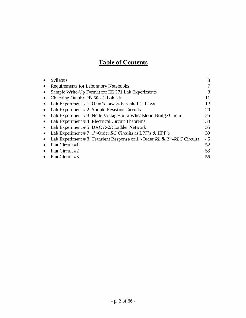
Table of Contents
Syllabus 3
Requirements for Laboratory Notebooks 7
Sample Write-Up Format for EE 271 Lab Experiments 8
Checking Out the PB-503-C Lab Kit 11
Lab Experiment # 1: Ohm’s Law & Kirchhoff’s Laws 12
Lab Experiment # 2: Simple Resistive Circuits 20
Lab Experiment # 3: Node Voltages of a Wheatstone-Bridge Circuit 25
Lab Experiment # 4: Electrical Circuit Theorems 30
Lab Experiment # 5: DAC R-2R Ladder Network 35
Lab Experiment # 7: 1st-Order RC Circuits as LPF’s & HPF’s 39
Lab Experiment # 8: Transient Response of 1st-Order RL & 2
nd-RLC Circuits 46
Fun Circuit #1 52
Fun Circuit #2 53
Fun Circuit #3 55
- p. 3 of 66 -
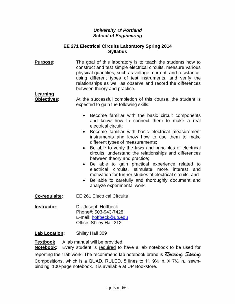
University f Portland School of Engineering
EE 271 Electrical Circuits Laboratory Spring 2014
Syllabus Purpose: The goal of this laboratory is to teach the students how to
construct and test simple electrical circuits, measure various physical quantities, such as voltage, current, and resistance, using different types of test instruments, and verify the relationships as well as observe and record the differences between theory and practice.
Learning Objectives: At the successful completion of this course, the student is
expected to gain the following skills:
Become familiar with the basic circuit components and know how to connect them to make a real electrical circuit;
Become familiar with basic electrical measurement instruments and know how to use them to make different types of measurements;
Be able to verify the laws and principles of electrical circuits, understand the relationships and differences between theory and practice;
Be able to gain practical experience related to electrical circuits, stimulate more interest and motivation for further studies of electrical circuits; and
Be able to carefully and thoroughly document and analyze experimental work.
Co-requisite: EE 261 Electrical Circuits
Instructor: Dr. Joseph Hoffbeck Phone#: 503-943-7428
E-mail: [email protected] Office: Shiley Hall 212
Lab Location: Shiley Hall 309
Textbook A lab manual will be provided. Notebook: Every student is required to have a lab notebook to be used for
reporting their lab work. The recommend lab notebook brand is Roaring Spring
Compositions, which is a QUAD. RULED, 5 lines to 1”, 9¾ in. X 7½ in., sewn-binding, 100-page notebook. It is available at UP Bookstore.
- p. 4 of 66 -
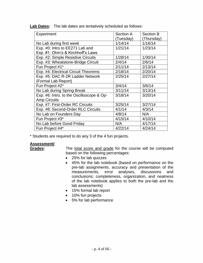
Lab Dates: The lab dates are tentatively scheduled as follows:
Experiment Section A (Tuesday)
Section B (Thursday)
No Lab during first week 1/14/14 1/16/14
Exp. #0: Intro to EE271 Lab and Exp. #1: Ohm’s & Kirchhoff’s Laws
1/21/14 1/23/14
Exp. #2: Simple Resistive Circuits 1/28/14 1/30/14
Exp. #3: Wheatstone-Bridge Circuit 2/4/14 2/6/14
Fun Project #1* 2/11/14 2/13/14
Exp. #4: Electrical Circuit Theorems 2/18/14 2/20/14
Exp. #5: DAC R-2R Ladder Network (Formal Lab Report)
2/25/14 2/27/14
Fun Project #2* 3/4/14 3/6/14
No Lab during Spring Break 3/11/14 3/13/14
Exp. #6: Intro. to the Oscilloscope & Op-Amp Circuits
3/18/14 3/20/14
Exp. #7: First-Order RC Circuits 3/25/14 3/27/14
Exp. #8: Second-Order RLC Circuits 4/1/14 4/3/14
No Lab on Founders Day 4/8/14 N/A
Fun Project #3* 4/15/14 4/10/14
No Lab before Good Friday N/A 4/17/14
Fun Project #4* 4/22/14 4/24/14
* Students are required to do any 3 of the 4 fun projects.
Assessment/ Grades: The total score and grade for the course will be computed
based on the following percentages:
25% for lab quizzes
45% for the lab notebook (based on performance on the pre-lab assignments, accuracy and presentation of the measurements, error analyses, discussions and conclusions; completeness, organization, and neatness of the lab notebook applies to both the pre-lab and the lab assessments)
15% formal lab report
10% fun projects
5% for lab performance
- p. 5 of 66 -
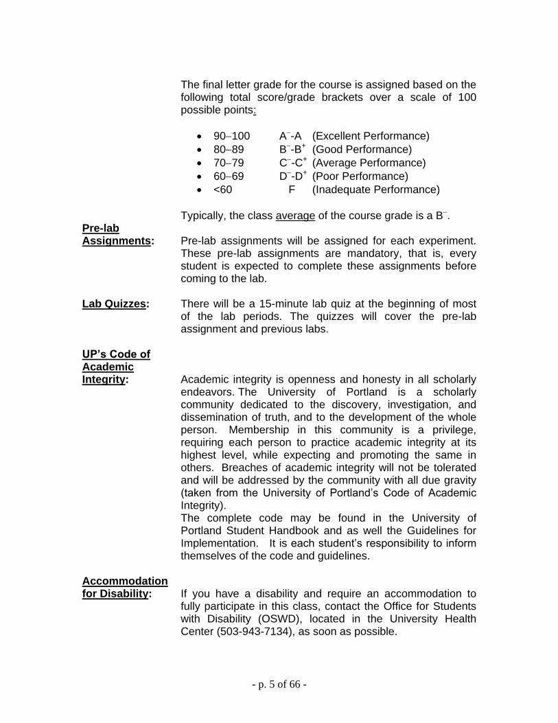
The final letter grade for the course is assigned based on the following total score/grade brackets over a scale of 100 possible points:
90100 A-A (Excellent Performance)
8089 B-B+ (Good Performance)
7079 C-C+ (Average Performance)
6069 D-D+ (Poor Performance)
<60 F (Inadequate Performance)
Typically, the class average of the course grade is a B. Pre-lab Assignments: Pre-lab assignments will be assigned for each experiment.
These pre-lab assignments are mandatory, that is, every student is expected to complete these assignments before coming to the lab.
Lab Quizzes: There will be a 15-minute lab quiz at the beginning of most
of the lab periods. The quizzes will cover the pre-lab assignment and previous labs.
UP’s Code of Academic Integrity: Academic integrity is openness and honesty in all scholarly
endeavors. The University of Portland is a scholarly community dedicated to the discovery, investigation, and dissemination of truth, and to the development of the whole person. Membership in this community is a privilege, requiring each person to practice academic integrity at its highest level, while expecting and promoting the same in others. Breaches of academic integrity will not be tolerated and will be addressed by the community with all due gravity (taken from the University of Portland’s Code of Academic Integrity). The complete code may be found in the University of Portland Student Handbook and as well the Guidelines for Implementation. It is each student’s responsibility to inform themselves of the code and guidelines.
Accommodation for Disability: If you have a disability and require an accommodation to
fully participate in this class, contact the Office for Students with Disability (OSWD), located in the University Health Center (503-943-7134), as soon as possible.
- p. 6 of 66 -
Assessment Disclosure: Student work products for this course may be used by the
University for educational quality assurance purposes. Diversity and Green Dot Statement: All persons should feel safe to express their opinions in my
class, regardless of their race, religion, political philosophy, gender, sexual orientation, or disability. In addition, I encourage anyone to speak up on behalf of themselves or others, if the classroom environment becomes uncomfortable for any reason.
Lab Safety: No one is allowed to work in the shops or labs without
appropriate training from the shop technician and without instructor permission. No food or beverages are allowed in the lab.
- p. 7 of 66 -
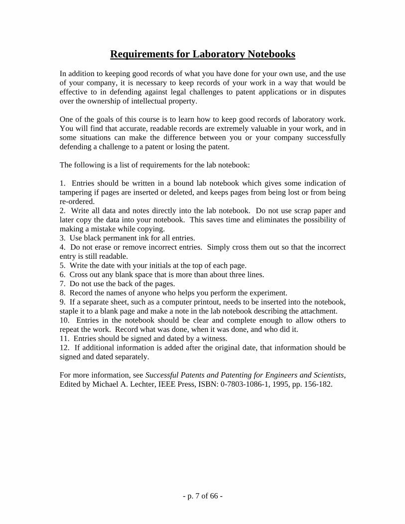
Requirements for Laboratory Notebooks
In addition to keeping good records of what you have done for your own use, and the use
of your company, it is necessary to keep records of your work in a way that would be
effective to in defending against legal challenges to patent applications or in disputes
over the ownership of intellectual property.
One of the goals of this course is to learn how to keep good records of laboratory work.
You will find that accurate, readable records are extremely valuable in your work, and in
some situations can make the difference between you or your company successfully
defending a challenge to a patent or losing the patent.
The following is a list of requirements for the lab notebook:
1. Entries should be written in a bound lab notebook which gives some indication of
tampering if pages are inserted or deleted, and keeps pages from being lost or from being
re-ordered.
2. Write all data and notes directly into the lab notebook. Do not use scrap paper and
later copy the data into your notebook. This saves time and eliminates the possibility of
making a mistake while copying.
3. Use black permanent ink for all entries.
4. Do not erase or remove incorrect entries. Simply cross them out so that the incorrect
entry is still readable.
5. Write the date with your initials at the top of each page.
6. Cross out any blank space that is more than about three lines.
7. Do not use the back of the pages.
8. Record the names of anyone who helps you perform the experiment.
9. If a separate sheet, such as a computer printout, needs to be inserted into the notebook,
staple it to a blank page and make a note in the lab notebook describing the attachment.
10. Entries in the notebook should be clear and complete enough to allow others to
repeat the work. Record what was done, when it was done, and who did it.
11. Entries should be signed and dated by a witness.
12. If additional information is added after the original date, that information should be
signed and dated separately.
For more information, see Successful Patents and Patenting for Engineers and Scientists,
Edited by Michael A. Lechter, IEEE Press, ISBN: 0-7803-1086-1, 1995, pp. 156-182.
- p. 8 of 66 -
Sample Write-Up Format for EE 271 Lab Experiments
The following is a sample write-up format for the EE 271 lab experiments. Please follow
this format for all your write-ups in your lab notebooks this semester. Note that the write-
up is provided in italics form.
SAMPLE LAB REPORT WRITE-UP
PROVIDE THE DATE! January 17, 2013 PROVIDE YOUR INITIALS!BF
PROVIDE THE TITLE! Experiment # 1: Ohm's Law and
Kirchhoff's Laws
I. Objective PROVIDE SUBTITLES!
In this experiment, the student will learn how to read resistor color codes and how to
measure voltage, current, and resistance with the digital multimeter (DMM). The student
will also build circuits and take measurements to verify Ohm's law, Kirchhoff's laws, and
the conservation of energy.
1(a)-Prelab Assignment:PROVIDE SUBTITLES! The color code for a 10 k
resistor with 5% tolerance will be Brown-Black-Orange-Gold.
VS=5 V R = 10 k
I
V
+
_
DRAW EACH CIRCUIT, PROVIDE
VOLTAGES (WITH POLARITIES),
CURRENTS (WITH DIRECTIONS), &
RESISTORS AS VARIABLES,
PROVIDE ALSO THEIR VALUES,
ETC. CLEARLY!I
ASSIGN FIGURE NUMBER AND
FIGURE TITLE (CAPTION) FOR
EACH FIGURE!
Figure 1. Circuit for pre-lab 1(a).
SHOW THE
REFERENCE NODE IN
EACH CIRCUIT!
Note that in Figure 1, the resistor voltage V=5 V based on KVL. In addition, note that the
currents of the voltage source and the resistor are equal based on KCL. Using Ohm’s
law, we can find the current I as (next page)
UNITS!EAPPROPRIAT PROVIDE 5.0 10
5 mA
kΩ
V
R
VI
- p. 9 of 66 -
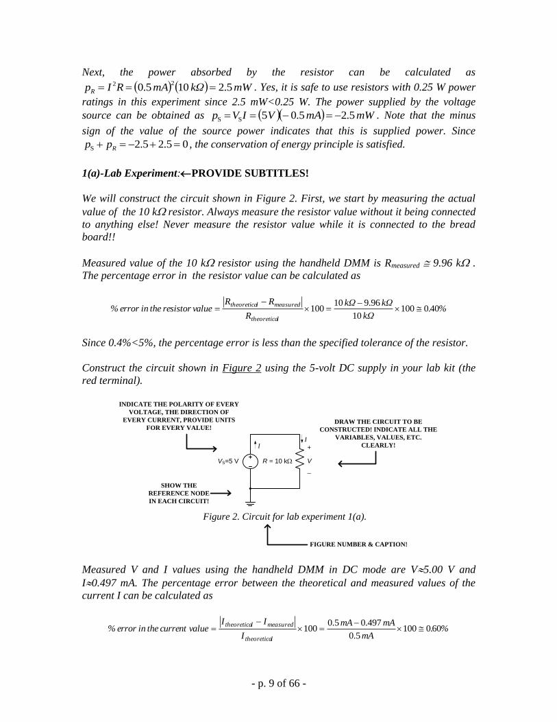
Next, the power absorbed by the resistor can be calculated as
mWkΩmARIpR 5.2 10 5.022 . Yes, it is safe to use resistors with 0.25 W power
ratings in this experiment since 2.5 mW<0.25 W. The power supplied by the voltage
source can be obtained as mWmAVIVp 5.2 5.0 5SS . Note that the minus
sign of the value of the source power indicates that this is supplied power. Since
05.25.2S Rpp , the conservation of energy principle is satisfied.
1(a)-Lab Experiment:PROVIDE SUBTITLES!
We will construct the circuit shown in Figure 2. First, we start by measuring the actual
value of the 10 k resistor. Always measure the resistor value without it being connected
to anything else! Never measure the resistor value while it is connected to the bread
board!!
Measured value of the 10 k resistor using the handheld DMM is Rmeasured 9.96 k .
The percentage error in the resistor value can be calculated as
%.kΩ
kΩkΩ
R
RRvalueresistortheinerror%
ltheoretica
measuredltheoretica400100
10
96.9 10100
Since 0.4%<5%, the percentage error is less than the specified tolerance of the resistor.
Construct the circuit shown in Figure 2 using the 5-volt DC supply in your lab kit (the
red terminal).
VS=5 V R = 10 k
I
V
+
_
DRAW THE CIRCUIT TO BE
CONSTRUCTED! INDICATE ALL THE
VARIABLES, VALUES, ETC.
CLEARLY!I
INDICATE THE POLARITY OF EVERY
VOLTAGE, THE DIRECTION OF
EVERY CURRENT, PROVIDE UNITS
FOR EVERY VALUE!
SHOW THE
REFERENCE NODE
IN EACH CIRCUIT!
Figure 2. Circuit for lab experiment 1(a).
FIGURE NUMBER & CAPTION!
Measured V and I values using the handheld DMM in DC mode are V5.00 V and
I0.497 mA. The percentage error between the theoretical and measured values of the
current I can be calculated as
%.mA
mAmA
I
IIvaluecurrenttheinerror%
ltheoretica
measuredltheoretica600100
5.0
497.0 5.0100
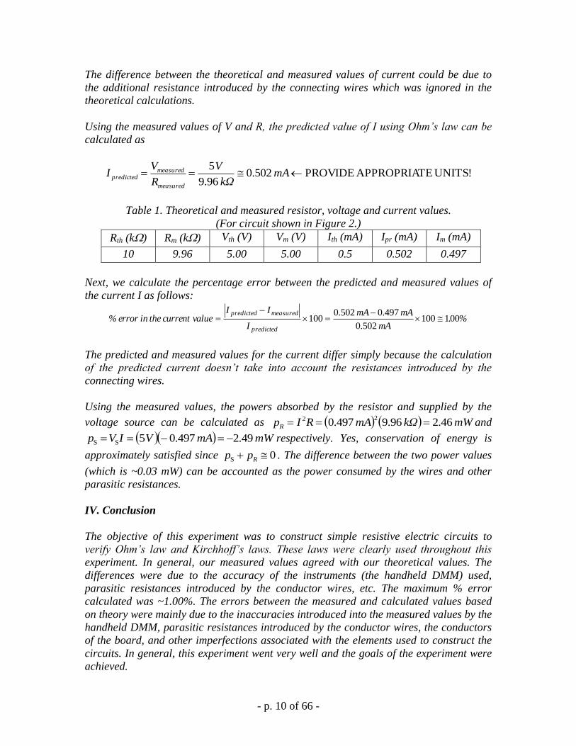
- p. 10 of 66 -
The difference between the theoretical and measured values of current could be due to
the additional resistance introduced by the connecting wires which was ignored in the
theoretical calculations.
Using the measured values of V and R, the predicted value of I using Ohm’s law can be
calculated as
UNITS! TE APPROPRIAPROVIDE 502.0 .969
5 mA
kΩ
V
R
VI
measured
measuredpredicted
Table 1. Theoretical and measured resistor, voltage and current values.
(For circuit shown in Figure 2.)
Rth (k) Rm (k) Vth (V) Vm (V) Ith (mA) Ipr (mA) Im (mA)
10 9.96 5.00 5.00 0.5 0.502 0.497
Next, we calculate the percentage error between the predicted and measured values of
the current I as follows:
%.mA
mAmA
I
IIvaluecurrenttheinerror%
predicted
measuredpredicted001100
502.0
497.0 502.0100
The predicted and measured values for the current differ simply because the calculation
of the predicted current doesn’t take into account the resistances introduced by the
connecting wires.
Using the measured values, the powers absorbed by the resistor and supplied by the
voltage source can be calculated as mWkΩmARIpR 46.2 .969 497.022 and
mWmAVIVp 49.2 497.0 5SS respectively. Yes, conservation of energy is
approximately satisfied since 0S Rpp . The difference between the two power values
(which is ~0.03 mW) can be accounted as the power consumed by the wires and other
parasitic resistances.
IV. Conclusion
The objective of this experiment was to construct simple resistive electric circuits to
verify Ohm’s law and Kirchhoff’s laws. These laws were clearly used throughout this
experiment. In general, our measured values agreed with our theoretical values. The
differences were due to the accuracy of the instruments (the handheld DMM) used,
parasitic resistances introduced by the conductor wires, etc. The maximum % error
calculated was ~1.00%. The errors between the measured and calculated values based
on theory were mainly due to the inaccuracies introduced into the measured values by the
handheld DMM, parasitic resistances introduced by the conductor wires, the conductors
of the board, and other imperfections associated with the elements used to construct the
circuits. In general, this experiment went very well and the goals of the experiment were
achieved.
- p. 11 of 66 -
Checking Out the PB-503-C Lab Kit
In order to become familiar with the lab kit, and to ensure that it is operating properly, please
read pages 4 and 5 in the PB-503-C Instruction Manual, do the following tests, and record
your measurements and results in your lab notebook:
Record the Kit number that is on the outside of the lab kit.
Measure the voltage between the terminal indicated as +5 V (it’s the red-colored
terminal near the upper right hand corner) and the ground terminal (black-colored
terminal near the upper right hand corner).
Measure the minimum and maximum voltages available between the yellow-colored
terminal near the upper right hand corner (labeled either +5 to 15 V or +1.3 to 15 V)
and ground terminal while adjusting the +15 V adjustment knob (small black-colored
knob near the top).
Measure the minimum and maximum voltages available between the blue-colored
terminal near the upper right hand corner (labeled either 5 to 15 V or 1.3 to 15
V) and ground terminal while adjusting the 15 V adjustment knob (small black-
colored knob near the top).
Test each LED by simply connecting its input to the +5 V terminal. Note that the
other terminals of the LED's are connected to ground internally.
Test the function generator by connecting the output (use the output on the right side,
NOT the TTL output) to one of the speaker inputs, and connect the other speaker
input to the ground terminal. Set the function generator switch on the left to KHz and
the switch on the right to 1. Slide the FREQ control to 1.0 and slide the amplitude
control to the top. Do you hear a tone? Switch the lower switch between square,
triangle, and sine waveforms. Do you hear a difference? (You may want to display
the different waveforms on the oscilloscope and measure the frequency.)
Test the 10K potentiometer (labeled as 10K POT) by measuring the minimum and
maximum resistance values between pins 1 and 2 while adjusting the knob. Also
measure the minimum and maximum resistance between pins 2 and 3, and between
pins 1 and 3.
Test the 1K potentiometer (labeled as 1K POT) by measuring the minimum and
maximum resistances available between pins 1 and 2 while adjusting the knob.
Similarly, measure the minimum and maximum resistances between pins 2 and 3, and
between pins 1 and 3.
Are you finished early? Try these optional experiments:
Measure the maximum frequency that an LED can flash and still perceived to be as
flashing by connecting the TTL output of the function generator to one of the LED's.
Find the minimum and maximum frequencies that you can hear from the speaker by
connecting the function generator output (use the output on the right side, NOT the
TTL output) to one of the speaker inputs, connect the other speaker input to ground,
and set the waveform to sine.
- p. 12 of 66 -
University f Prtland
Schl f Engineering
EE 271Electrical Circuits Laboratory
Lab Experiment #1: Ohm's Law and
Kirchhoff's Laws
- p. 13 of 66 -
Ohm's Law and Kirchhoff's Laws
I. Objective
In this experiment, the student will learn how to read resistor color codes and how to
measure voltage, current, and resistance with the digital multimeter (DMM). The student
will also build circuits and take measurements to verify Ohm's law, Kirchhoff's laws, and
the conservation of energy.
II. Background: Resistor Color Codes
Standard resistors are labeled with a color code which indicates their resistance values.
The value indicated by each color band is listed in Tables 1, 2, and 3, and the resistor's
value can be computed by the following equation:
1st Digit 10 2nd Digit MultiplierR
Consider a resistor that has the following color bands: brown, green, orange, and silver.
We first recognize that the silver band must be the tolerance band since the 1st Digit
cannot be silver (see Tables 1 and 2). So the brown band must be the 1st band, which
indicates that the value of the 1st Digit equals 1 (see Table 2). The second band, then, is
green, which indicates that the value of the 2nd Digit equals 5 (see Table 2). The
multiplier band is orange which indicates a value of 1 k (see Table 3). So the value of
this resistor is 1 10 5 1k 15 kR . Furthermore, the silver tolerance band
indicates that the actual value of the resistance might deviate by %10 (see Table 1).
A resistor with the bands red, violet, red, gold, would have a value of
2 10 7 100 2700 2.7 kR with a tolerance of %5 .
A resistor with the bands orange, orange, brown, gold, would have a value of
3 10 3 10 330R with a tolerance of %5 .
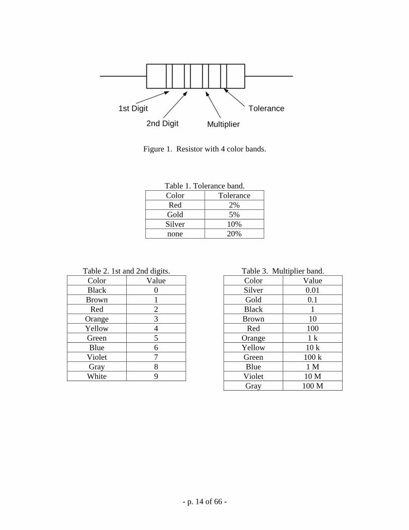
- p. 14 of 66 -
Tolerance1st Digit
2nd Digit Multiplier
Figure 1. Resistor with 4 color bands.
Table 1. Tolerance band.
Color Tolerance
Red 2%
Gold 5%
Silver 10%
none 20%
Table 2. 1st and 2nd digits.
Color Value
Black 0
Brown 1
Red 2
Orange 3
Yellow 4
Green 5
Blue 6
Violet 7
Gray 8
White 9
Table 3. Multiplier band.
Color Value
Silver 0.01
Gold 0.1
Black 1
Brown 10
Red 100
Orange 1 k
Yellow 10 k
Green 100 k
Blue 1 M
Violet 10 M
Gray 100 M
- p. 15 of 51-
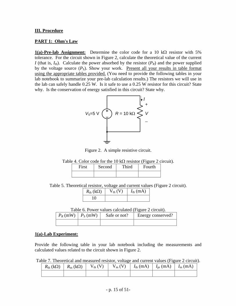
III. Procedure
PART 1: Ohm's Law
1(a)-Pre-lab Assignment: Determine the color code for a 10 k resistor with 5%
tolerance. For the circuit shown in Figure 2, calculate the theoretical value of the current
I (that is, Ith). Calculate the power absorbed by the resistor (PR) and the power supplied
by the voltage source (PS). Show your work. Present all your results in table format
using the appropriate tables provided. (You need to provide the following tables in your
lab notebook to summarize your pre-lab calculation results.) The resistors we will use in
the lab can safely handle 0.25 W. Is it safe to use a 0.25 W resistor for this circuit? State
why. Is the conservation of energy satisfied in this circuit? State why.
VS=5 V R = 10 k
I
V
+
_
Figure 2. A simple resistive circuit.
Table 4. Color code for the 10 k resistor (Figure 2 circuit).
First Second Third Fourth
Table 5. Theoretical resistor, voltage and current values (Figure 2 circuit).
Rth (k) Vth (V) Ith (mA)
10
Table 6. Power values calculated (Figure 2 circuit).
PR (mW) PS (mW) Safe or not? Energy conserved?
1(a)-Lab Experiment:
Provide the following table in your lab notebook including the measurements and
calculated values related to the circuit shown in Figure 2.
Table 7. Theoretical and measured resistor, voltage and current values (Figure 2 circuit).
Rth (k) Rm (k) Vth (V) Vm (V) Ith (mA) Ipr (mA) Im (mA)
- p. 16 of 51-
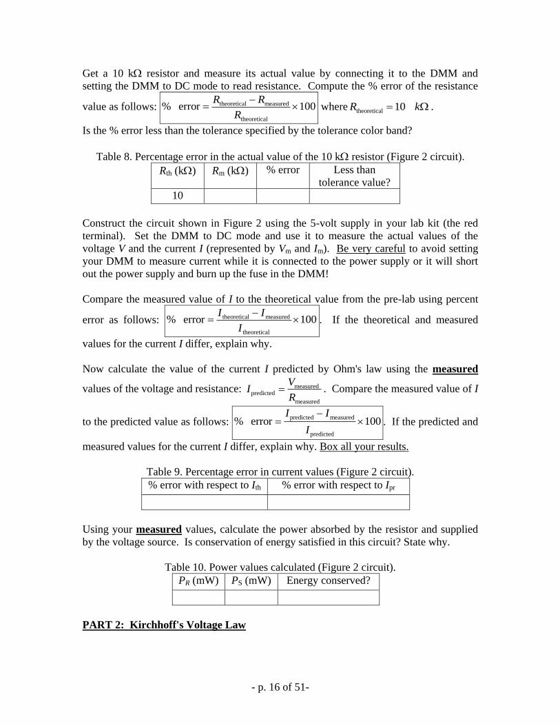
Get a 10 k resistor and measure its actual value by connecting it to the DMM and
setting the DMM to DC mode to read resistance. Compute the % error of the resistance
value as follows: theoretical measured
theoretical
% error 100R R
R
where
theoretical 10R k .
Is the % error less than the tolerance specified by the tolerance color band?
Table 8. Percentage error in the actual value of the 10 k resistor (Figure 2 circuit).
Rth (k) Rm (k) % error Less than
tolerance value?
10
Construct the circuit shown in Figure 2 using the 5-volt supply in your lab kit (the red
terminal). Set the DMM to DC mode and use it to measure the actual values of the
voltage V and the current I (represented by Vm and Im). Be very careful to avoid setting
your DMM to measure current while it is connected to the power supply or it will short
out the power supply and burn up the fuse in the DMM!
Compare the measured value of I to the theoretical value from the pre-lab using percent
error as follows: theoretical measured
theoretical
% error 100I I
I
. If the theoretical and measured
values for the current I differ, explain why.
Now calculate the value of the current I predicted by Ohm's law using the measured
values of the voltage and resistance: measuredpredicted
measured
VI
R . Compare the measured value of I
to the predicted value as follows: predicted measured
predicted
% error 100I I
I
. If the predicted and
measured values for the current I differ, explain why. Box all your results.
Table 9. Percentage error in current values (Figure 2 circuit).
% error with respect to Ith % error with respect to Ipr
Using your measured values, calculate the power absorbed by the resistor and supplied
by the voltage source. Is conservation of energy satisfied in this circuit? State why.
Table 10. Power values calculated (Figure 2 circuit).
PR (mW) PS (mW) Energy conserved?
PART 2: Kirchhoff's Voltage Law
- p. 17 of 51-
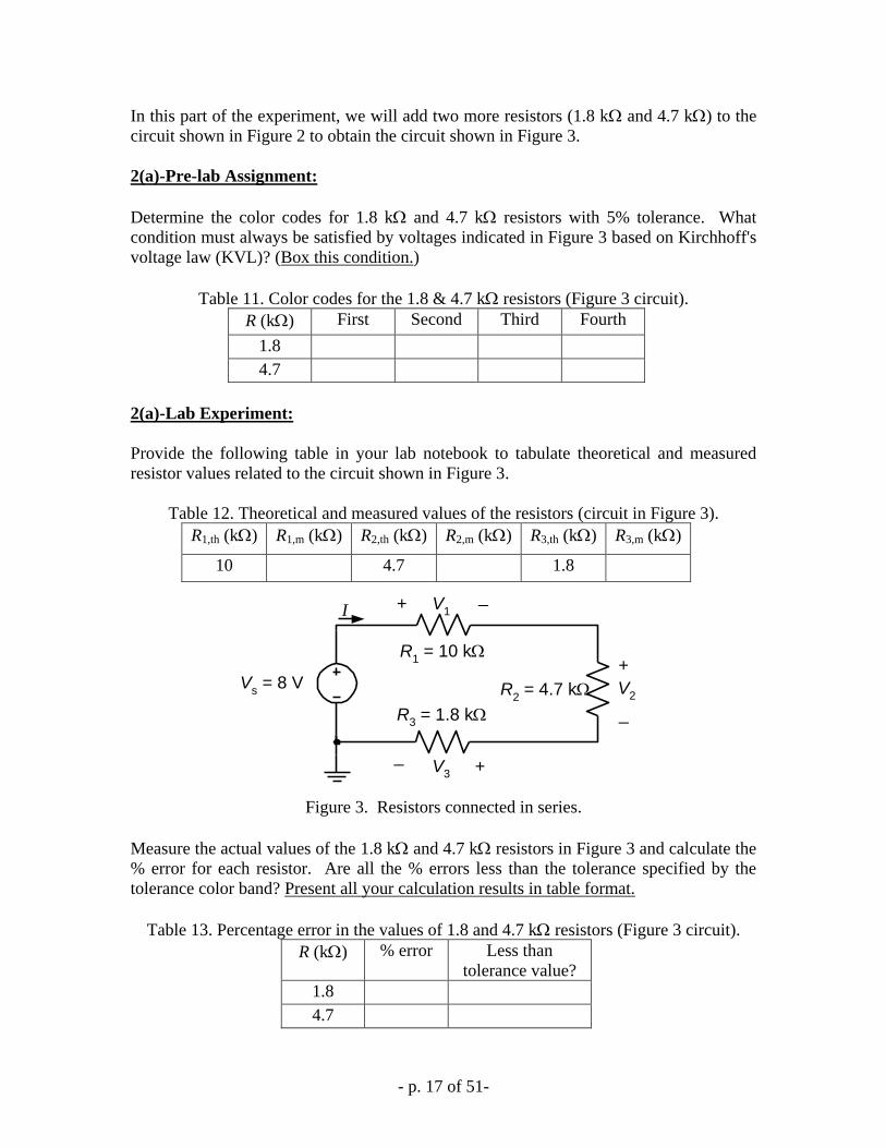
In this part of the experiment, we will add two more resistors (1.8 k and 4.7 k) to the
circuit shown in Figure 2 to obtain the circuit shown in Figure 3.
2(a)-Pre-lab Assignment:
Determine the color codes for 1.8 k and 4.7 k resistors with 5% tolerance. What
condition must always be satisfied by voltages indicated in Figure 3 based on Kirchhoff's
voltage law (KVL)? (Box this condition.)
Table 11. Color codes for the 1.8 & 4.7 k resistors (Figure 3 circuit).
R (k) First Second Third Fourth
1.8
4.7
2(a)-Lab Experiment:
Provide the following table in your lab notebook to tabulate theoretical and measured
resistor values related to the circuit shown in Figure 3.
Table 12. Theoretical and measured values of the resistors (circuit in Figure 3).
R1,th (k) R1,m (k) R2,th (k) R2,m (k) R3,th (k) R3,m (k)
10 4.7 1.8
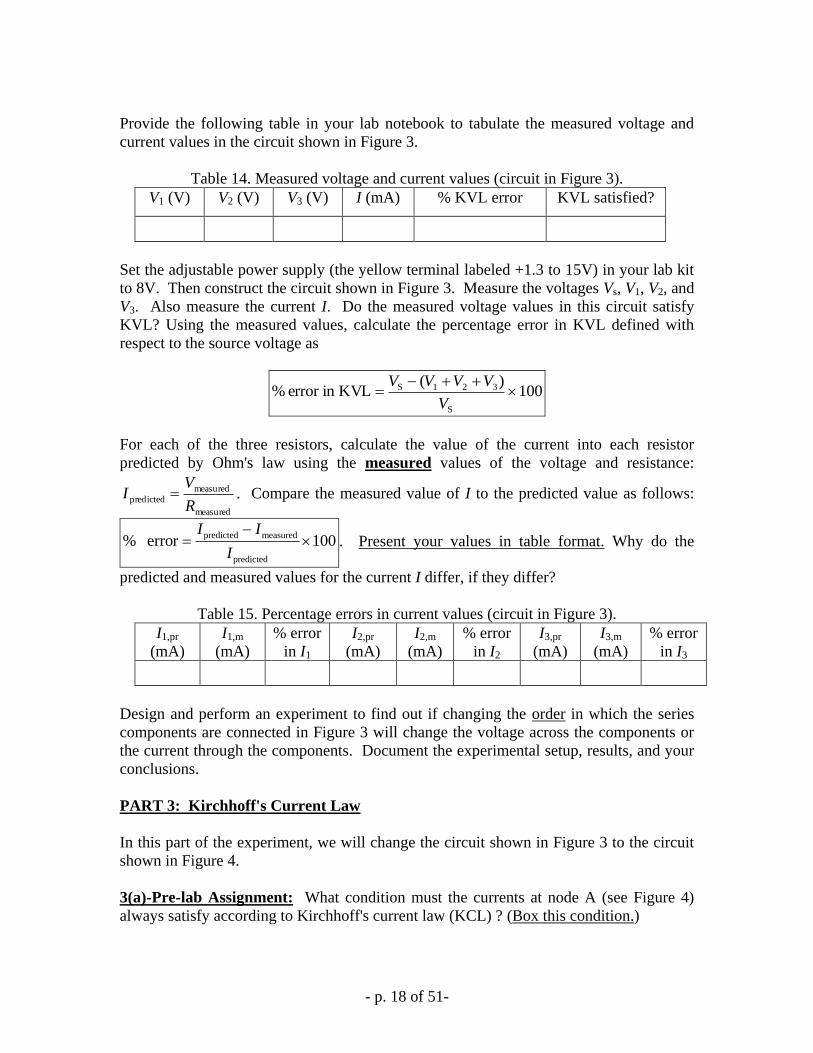
Vs = 8 V
R1 = 10 k
R2 = 4.7 k
R3 = 1.8 k
I V1
V3
V2
+ _
+
_
+_
Figure 3. Resistors connected in series.
Measure the actual values of the 1.8 k and 4.7 k resistors in Figure 3 and calculate the
% error for each resistor. Are all the % errors less than the tolerance specified by the
tolerance color band? Present all your calculation results in table format.
Table 13. Percentage error in the values of 1.8 and 4.7 k resistors (Figure 3 circuit).
R (k) % error Less than
tolerance value?
1.8
4.7
- p. 18 of 51-
Provide the following table in your lab notebook to tabulate the measured voltage and
current values in the circuit shown in Figure 3.
Table 14. Measured voltage and current values (circuit in Figure 3).
V1 (V) V2 (V) V3 (V) I (mA) % KVL error KVL satisfied?
Set the adjustable power supply (the yellow terminal labeled +1.3 to 15V) in your lab kit
to 8V. Then construct the circuit shown in Figure 3. Measure the voltages Vs, V1, V2, and
V3. Also measure the current I. Do the measured voltage values in this circuit satisfy
KVL? Using the measured values, calculate the percentage error in KVL defined with
respect to the source voltage as
100)(
KVLinerror %S
321S
V
VVVV
For each of the three resistors, calculate the value of the current into each resistor
predicted by Ohm's law using the measured values of the voltage and resistance:
measured
measured
predictedR
VI . Compare the measured value of I to the predicted value as follows:
predicted measured
predicted
% error 100I I
I
. Present your values in table format. Why do the
predicted and measured values for the current I differ, if they differ?
Table 15. Percentage errors in current values (circuit in Figure 3).
I1,pr
(mA)
I1,m
(mA)
% error
in I1
I2,pr
(mA)
I2,m
(mA)
% error
in I2
I3,pr
(mA)
I3,m
(mA)
% error
in I3
Design and perform an experiment to find out if changing the order in which the series
components are connected in Figure 3 will change the voltage across the components or
the current through the components. Document the experimental setup, results, and your
conclusions.
PART 3: Kirchhoff's Current Law
In this part of the experiment, we will change the circuit shown in Figure 3 to the circuit
shown in Figure 4.
3(a)-Pre-lab Assignment: What condition must the currents at node A (see Figure 4)
always satisfy according to Kirchhoff's current law (KCL) ? (Box this condition.)
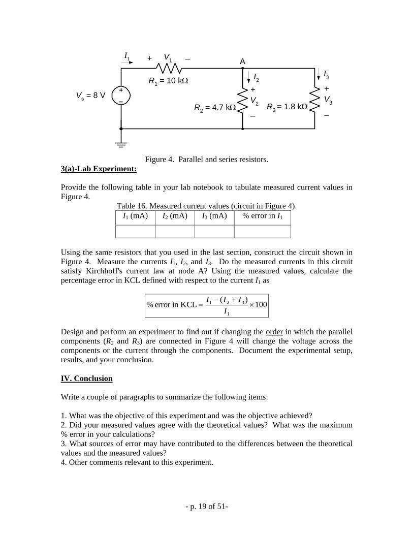
- p. 19 of 51-
Vs = 8 V
R1 = 10 k
R2 = 4.7 k
I1 V
1
V2
+ _
+
_R
3 = 1.8 k
V3
+
_
I2
I3
A
Figure 4. Parallel and series resistors.
3(a)-Lab Experiment:
Provide the following table in your lab notebook to tabulate measured current values in
Figure 4.
Table 16. Measured current values (circuit in Figure 4).
I1 (mA) I2 (mA) I3 (mA) % error in I1
Using the same resistors that you used in the last section, construct the circuit shown in
Figure 4. Measure the currents I1, I2, and I3. Do the measured currents in this circuit
satisfy Kirchhoff's current law at node A? Using the measured values, calculate the
percentage error in KCL defined with respect to the current I1 as
100)(
KCLinerror %1
321
I
III
Design and perform an experiment to find out if changing the order in which the parallel
components (R2 and R3) are connected in Figure 4 will change the voltage across the
components or the current through the components. Document the experimental setup,
results, and your conclusion.
IV. Conclusion
Write a couple of paragraphs to summarize the following items:
1. What was the objective of this experiment and was the objective achieved?
2. Did your measured values agree with the theoretical values? What was the maximum
% error in your calculations?
3. What sources of error may have contributed to the differences between the theoretical
values and the measured values?
4. Other comments relevant to this experiment.
- p. 20 of 51-
University f Prtland
Schl f Engineering
EE 271Electrical Circuits Laboratory
Lab Experiment #2: Simple Resistive
Circuits
- p. 21 of 51-
Simple Resistive Circuits
I. Objective
In this experiment, the students will design, build and/or experiment simple
resistive electrical circuits to gain some experience in using Ohm’s law,
Kirchhoff’s laws, and their extensions such as voltage and current divider
principles to analyze circuits consisting of series- and parallel-connected resistors.
II. Procedure
PART 1: Voltage and Current Divider Principles
Part 1(a): Verification of the Voltage Divider Circuit
1(a)Pre-lab Assignment: For the circuit shown in Fig. 1(a), using the voltage
divider principle, provide a general equation for Vout and calculate its numerical
value. Box your answer.
1(a)Lab Experiment: Construct the circuit shown in Fig. 1(a). Using the
handheld DMM in DC mode set to read resistance, measure and record the actual
values of the resistors R1 and R2 used in your circuit in Table 1. Calculate the %
error in each resistor value as follows:
100 value inerror %ltheoretica
measuredltheoretica
R
RRR
Table 1. Resistor values and percentage errors. (Circuit in Figure 1(a).)
R1 (k)
(theoretical)
R1 (k)
(measured)
% error in
R1 R2 (k)
(theoretical)
R2 (k)
(measured)
% error in
R2
Provide the calculated percentage errors in the resistor values in Table 1. Measure
and record the output voltage Vout. Also calculate the % error of the Vout value as
follows:
100 value inerror %prelab out,
measured out,prelab out,
out
V
VVV
Box your results. Comment on the differences between the theoretical and
measured values.
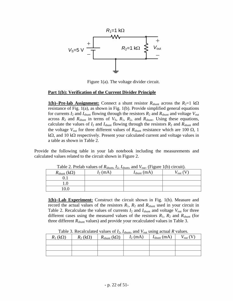
- p. 22 of 51-
VS=5 V
R1=1 k
R2=1 k Vout
Figure 1(a). The voltage divider circuit.
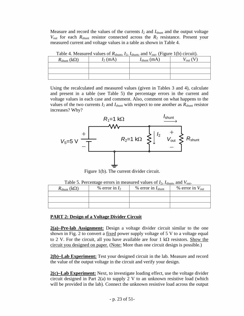
Part 1(b): Verification of the Current Divider Principle
1(b)Pre-lab Assignment: Connect a shunt resistor Rshunt across the R2=1 k
resistance of Fig. 1(a), as shown in Fig. 1(b). Provide simplified general equations
for currents I2 and Ishunt flowing through the resistors R2 and Rshunt and voltage Vout
across R2 and Rshunt in terms of VS, R1, R2, and Rshunt. Using these equations,
calculate the values of I2 and Ishunt flowing through the resistors R2 and Rshunt and
the voltage Vout for three different values of Rshunt resistance which are 100 , 1
k, and 10 k respectively. Present your calculated current and voltage values in
a table as shown in Table 2.
Provide the following table in your lab notebook including the measurements and
calculated values related to the circuit shown in Figure 2.
Table 2. Prelab values of Rshunt, I2, Ishunt, and Vout. (Figure 1(b) circuit).
Rshunt (k) I2 (mA) Ishunt (mA) Vout (V)
0.1
1.0
10.0
1(b)Lab Experiment: Construct the circuit shown in Fig. 1(b). Measure and
record the actual values of the resistors R1, R2 and Rshunt used in your circuit in
Table 2. Recalculate the values of currents I2 and Ishunt and voltage Vout for three
different cases using the measured values of the resistors R1, R2 and Rshunt (for
three different Rshunt values) and provide your recalculated values in Table 3.
Table 3. Recalculated values of I2, Ishunt, and Vout using actual R values.
R1 (k) R2 (k) Rshunt (k) I2 (mA) Ishunt (mA) Vout (V)
- p. 23 of 51-
Measure and record the values of the currents I2 and Ishunt and the output voltage
Vout for each Rshunt resistor connected across the R2 resistance. Present your
measured current and voltage values in a table as shown in Table 4.
Table 4. Measured values of Rshunt, I2, Ishunt, and Vout. (Figure 1(b) circuit).
Rshunt (k) I2 (mA) Ishunt (mA) Vout (V)
Using the recalculated and measured values (given in Tables 3 and 4), calculate
and present in a table (see Table 5) the percentage errors in the current and
voltage values in each case and comment. Also, comment on what happens to the
values of the two currents I2 and Ishunt with respect to one another as Rshunt resistor
increases? Why?
VS=5 V
R1=1 k
R2=1 k RshuntVout
Ishunt
I2
Figure 1(b). The current divider circuit.
Table 5. Percentage errors in measured values of I2, Ishunt, and Vout.
Rshunt (k) % error in I2 % error in Ishunt % error in Vout
PART 2: Design of a Voltage Divider Circuit
2(a)Pre-lab Assignment: Design a voltage divider circuit similar to the one
shown in Fig. 2 to convert a fixed power supply voltage of 5 V to a voltage equal
to 2 V. For the circuit, all you have available are four 1 k resistors. Show the
circuit you designed on paper. (Note: More than one circuit design is possible.)
2(b)Lab Experiment: Test your designed circuit in the lab. Measure and record
the value of the output voltage in the circuit and verify your design.
2(c)Lab Experiment: Next, to investigate loading effect, use the voltage divider
circuit designed in Part 2(a) to supply 2 V to an unknown resistive load (which
will be provided in the lab). Connect the unknown resistive load across the output
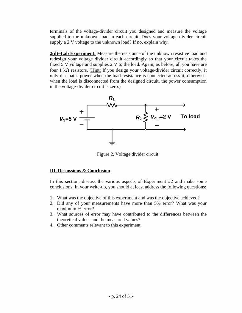
- p. 24 of 51-
terminals of the voltage-divider circuit you designed and measure the voltage
supplied to the unknown load in each circuit. Does your voltage divider circuit
supply a 2 V voltage to the unknown load? If no, explain why.
2(d)Lab Experiment: Measure the resistance of the unknown resistive load and
redesign your voltage divider circuit accordingly so that your circuit takes the
fixed 5 V voltage and supplies 2 V to the load. Again, as before, all you have are
four 1 k resistors. (Hint: If you design your voltage-divider circuit correctly, it
only dissipates power when the load resistance is connected across it, otherwise,
when the load is disconnected from the designed circuit, the power consumption
in the voltage-divider circuit is zero.)
VS=5 V
R1
R2 Vout=2 V To load
Figure 2. Voltage divider circuit.
III. Discussions & Conclusion
In this section, discuss the various aspects of Experiment #2 and make some
conclusions. In your write-up, you should at least address the following questions:
1. What was the objective of this experiment and was the objective achieved?
2. Did any of your measurements have more than 5% error? What was your
maximum % error?
3. What sources of error may have contributed to the differences between the
theoretical values and the measured values?
4. Other comments relevant to this experiment.
- p. 25 of 51-
University f Prtland
Schl f Engineering
EE 271Electrical Circuits Laboratory
Lab Experiment #3: Node Voltages of a
Wheatstone Bridge Circuit
- p. 26 of 51-
Node Voltages of a Wheatstone Bridge Circuit
I. Objective
In this experiment, the students will construct and test a Wheatstone bridge
circuit. In addition, they will use a Wheatstone bridge circuit to measure the value
of an unknown resistance.
II. History
Wheatstone bridge is an electrical circuit that can be used for measuring the value
of an electrical resistance in a circuit. This circuit is named after Sir Charles
Wheatstone (1802-1875), an English physicist and inventor who was a major
figure in Victorian science. Wheatstone studied electricity and became a professor
of experimental philosophy at King’s College, University of London in 1834. He
worked with William Cooke to produce the electric telegraph (1837), which some
people refer to as the “Victorian Internet”! In 1838, he invented the stereoscope.
Wheatstone is best remembered for the Wheatstone bridge circuit. The
Wheatstone bridge circuit was first described by Samuel Hunter Christie (1784-
1865) in his paper Experimental Determination of the Laws of Magneto-electric
Induction published in 1833. Wheatstone introduced this circuit in his Bakerian
Lecture on electrical measurements in 1843 and called it a Differential Resistance
Measurer. In his lecture, although Wheatstone publicly stated that the principle of
this circuit was not his own invention but it was rather an adaptation of a device
originally suggested by Christie, the circuit was still named after him because he
was the one who popularized it and put it in practical use. One such practical use
is measurements using strain gauges that exhibit small changes in electrical
resistance when strained as a result of stress.
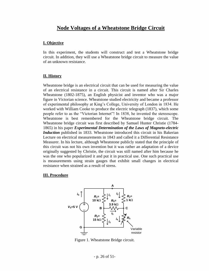
III. Procedure
R1=
10 k
VS=5 V
R2=
1 k
R3=
15 kR4
R5=
3.9 k
A
B C
G
iS i1i2
i3i4
i5
Variable
resistor
Figure 1. Wheatstone Bridge circuit.
- p. 27 of 51-
Pre-lab Assignment 1: A Wheatstone bridge circuit is shown in Fig. 1. This
circuit is said to be balanced Wheatstone bridge circuit when the current i5=0.
Determine the required relationship between the resistors R1, R2, R3, R4 and R5
needed to achieve this balanced circuit. (Hint: Note that i5=0 means VB=VC. That
is, resistor R5 acts like an open circuit. This means one can remove resistor R5
from the circuit as if nodes B and C are not connected at all. This removal will
simply the circuit and make it much easier to determine the relationship needed
between resistors R1, R2, R3, and R4 to achieve VB=VC.)
Lab Experiment 1: Constructing and testing a Wheatstone bridge circuit.
Construct the Wheatstone bridge circuit shown in Fig. 1 on your circuit board.
Record the actual values of all the resistors used in your circuit. Note that the
resistor R4 is a variable resistor. Use the following values for R4 (measure and
record their actual values): (a) R4=150 , (b) R4=1.5 k, and (c) R4=15 k. For
each R4 value used, do the following:
1. Use your handheld DMM available in your lab-kit to measure and record the
node voltages VA, VB, and VC. Present your measurements in table form as
shown.
2. Use the node voltages measured along with Ohm’s law and the actual resistor
values measured to calculate the currents i1, i2, i3, i4, and i5. For example, the
current i2 through the R2 resistance is given in terms of the node voltages as
2 A C 2i V V R . Present your calculated values in table form as shown.
3. Use the current values calculated in part 2 to verify Kirchhoff’s current law
(KCL) at nodes B and C.
Table 1. Measured node voltage and calculated current values (Figure 1 circuit
with R4 = 150 ).
VA (V) VB (V) VC (V) i1 (mA) i2 (mA) i3 (mA) i4 (mA) i5 (mA)
Table 2. Measured node voltage and calculated current values (Figure 1 circuit
with R4 = 1.5 k).
VA (V) VB (V) VC (V) i1 (mA) i2 (mA) i3 (mA) i4 (mA) i5 (mA)
Table 3. Measured node voltage and calculated current values (Figure 1 circuit
with R4 = 15 k).
VA (V) VB (V) VC (V) i1 (mA) i2 (mA) i3 (mA) i4 (mA) i5 (mA)
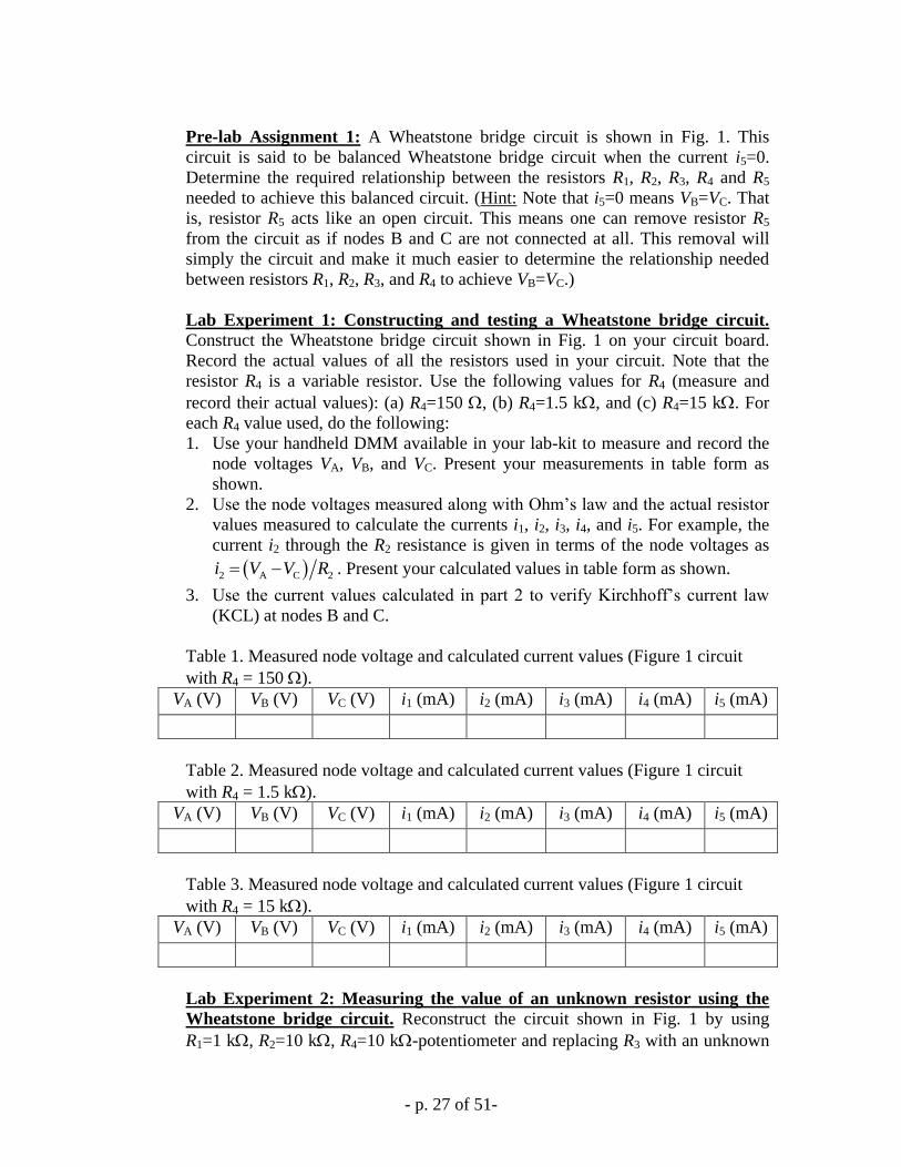
Lab Experiment 2: Measuring the value of an unknown resistor using the
Wheatstone bridge circuit. Reconstruct the circuit shown in Fig. 1 by using
R1=1 k, R2=10 k, R4=10 k-potentiometer and replacing R3 with an unknown
- p. 28 of 51-
resistor to be provided, as shown in Fig. 2. Keep the resistor R5 the same. Vary the
potentiometer resistance R4 until i5=0. Measure and record the value of R4 that
balances the bridge. Compute the value of the resistor R3 as determined by the
Wheatstone bridge. Measure R3 using the handheld DMM and compare it with the
calculated value. Calculate the percentage error in the R3 value using
100 value inerror %bridge3,
DMM3,bridge,3
3
R
RRR
R1=
1 k
VS=5 V
R2=
10 k
R3=? R4
R5=
3.9 k
A
B C
G
iS i1i2
i3i4
i5
10 k
potentiometer
Figure 2. Wheatstone Bridge circuit for Lab Experiment 2.
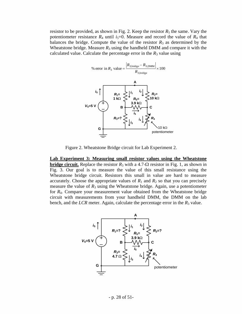
Lab Experiment 3: Measuring small resistor values using the Wheatstone
bridge circuit. Replace the resistor R3 with a 4.7- resistor in Fig. 1, as shown in
Fig. 3. Our goal is to measure the value of this small resistance using the
Wheatstone bridge circuit. Resistors this small in value are hard to measure
accurately. Choose the appropriate values of R1 and R2 so that you can precisely
measure the value of R3 using the Wheatstone bridge. Again, use a potentiometer
for R4. Compare your measurement value obtained from the Wheatstone bridge
circuit with measurements from your handheld DMM, the DMM on the lab
bench, and the LCR meter. Again, calculate the percentage error in the R3 value.
R1=?
VS=5 V
R2=?
R3=
4.7 R4
R5=
3.9 k
A
B C
G
iS i1i2
i3i4
i5
potentiometer
- p. 29 of 51-
Figure 3. Wheatstone Bridge circuit for Lab Experiment 3.
IV. Discussions & Conclusion
In this section, discuss the various aspects of Experiment #3 and make some
conclusions. In your write-up, you should at least address the following questions:
1. What was the objective of this experiment and was the objective achieved?
2. Did any of your measurements have more than 5% error? What was your
maximum % error?
3. What sources of error may have contributed to the differences between the
theoretical values and the measured values?
4. Other comments relevant to this experiment.
- p. 30 of 51-
University f Prtland
Schl f Engineering
EE 271Electrical Circuits Laboratory
Lab Experiment #4: Electrical Circuit
Theorems
- p. 31 of 51-
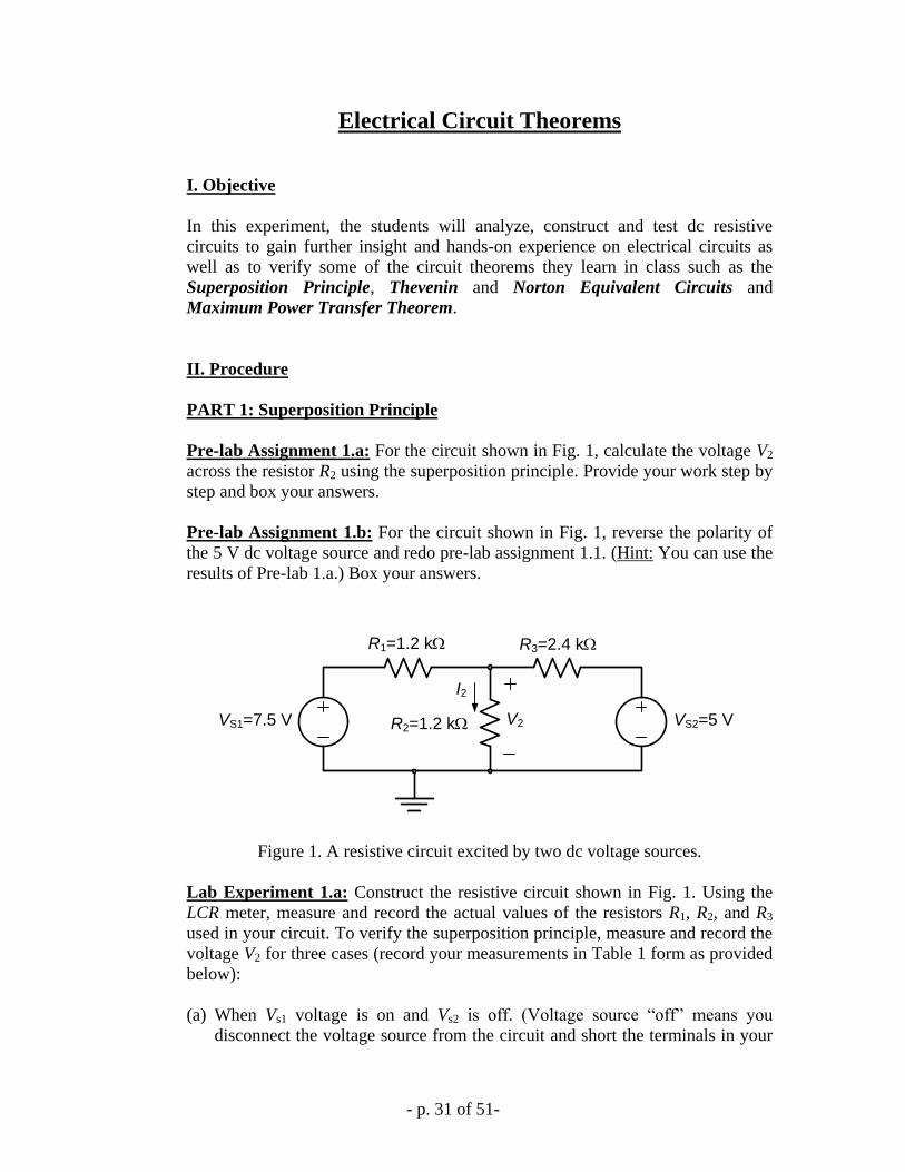
Electrical Circuit Theorems
I. Objective
In this experiment, the students will analyze, construct and test dc resistive
circuits to gain further insight and hands-on experience on electrical circuits as
well as to verify some of the circuit theorems they learn in class such as the
Superposition Principle, Thevenin and Norton Equivalent Circuits and
Maximum Power Transfer Theorem.
II. Procedure
PART 1: Superposition Principle
Pre-lab Assignment 1.a: For the circuit shown in Fig. 1, calculate the voltage V2
across the resistor R2 using the superposition principle. Provide your work step by
step and box your answers.
Pre-lab Assignment 1.b: For the circuit shown in Fig. 1, reverse the polarity of
the 5 V dc voltage source and redo pre-lab assignment 1.1. (Hint: You can use the
results of Pre-lab 1.a.) Box your answers.
VS1=7.5 V VS2=5 V
R1=1.2 k R3=2.4 k
R2=1.2 k
I2
V2
Figure 1. A resistive circuit excited by two dc voltage sources.
Lab Experiment 1.a: Construct the resistive circuit shown in Fig. 1. Using the
LCR meter, measure and record the actual values of the resistors R1, R2, and R3
used in your circuit. To verify the superposition principle, measure and record the
voltage V2 for three cases (record your measurements in Table 1 form as provided
below):
(a) When Vs1 voltage is on and Vs2 is off. (Voltage source “off” means you
disconnect the voltage source from the circuit and short the terminals in your
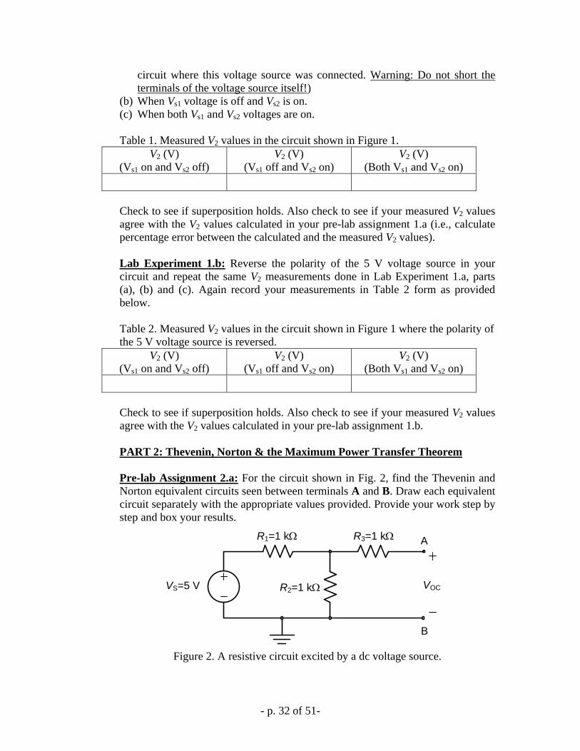
- p. 32 of 51-
circuit where this voltage source was connected. Warning: Do not short the
terminals of the voltage source itself!)
(b) When Vs1 voltage is off and Vs2 is on.
(c) When both Vs1 and Vs2 voltages are on.
Table 1. Measured V2 values in the circuit shown in Figure 1.
V2 (V)
(Vs1 on and Vs2 off)
V2 (V)
(Vs1 off and Vs2 on)
V2 (V)
(Both Vs1 and Vs2 on)
Check to see if superposition holds. Also check to see if your measured V2 values
agree with the V2 values calculated in your pre-lab assignment 1.a (i.e., calculate
percentage error between the calculated and the measured V2 values).
Lab Experiment 1.b: Reverse the polarity of the 5 V voltage source in your
circuit and repeat the same V2 measurements done in Lab Experiment 1.a, parts
(a), (b) and (c). Again record your measurements in Table 2 form as provided
below.
Table 2. Measured V2 values in the circuit shown in Figure 1 where the polarity of
the 5 V voltage source is reversed.
V2 (V)
(Vs1 on and Vs2 off)
V2 (V)
(Vs1 off and Vs2 on)
V2 (V)
(Both Vs1 and Vs2 on)
Check to see if superposition holds. Also check to see if your measured V2 values
agree with the V2 values calculated in your pre-lab assignment 1.b.
PART 2: Thevenin, Norton & the Maximum Power Transfer Theorem
Pre-lab Assignment 2.a: For the circuit shown in Fig. 2, find the Thevenin and
Norton equivalent circuits seen between terminals A and B. Draw each equivalent
circuit separately with the appropriate values provided. Provide your work step by
step and box your results.
VS=5 V
R1=1 k R3=1 k
R2=1 k VOC
A
B
Figure 2. A resistive circuit excited by a dc voltage source.
- p. 33 of 51-
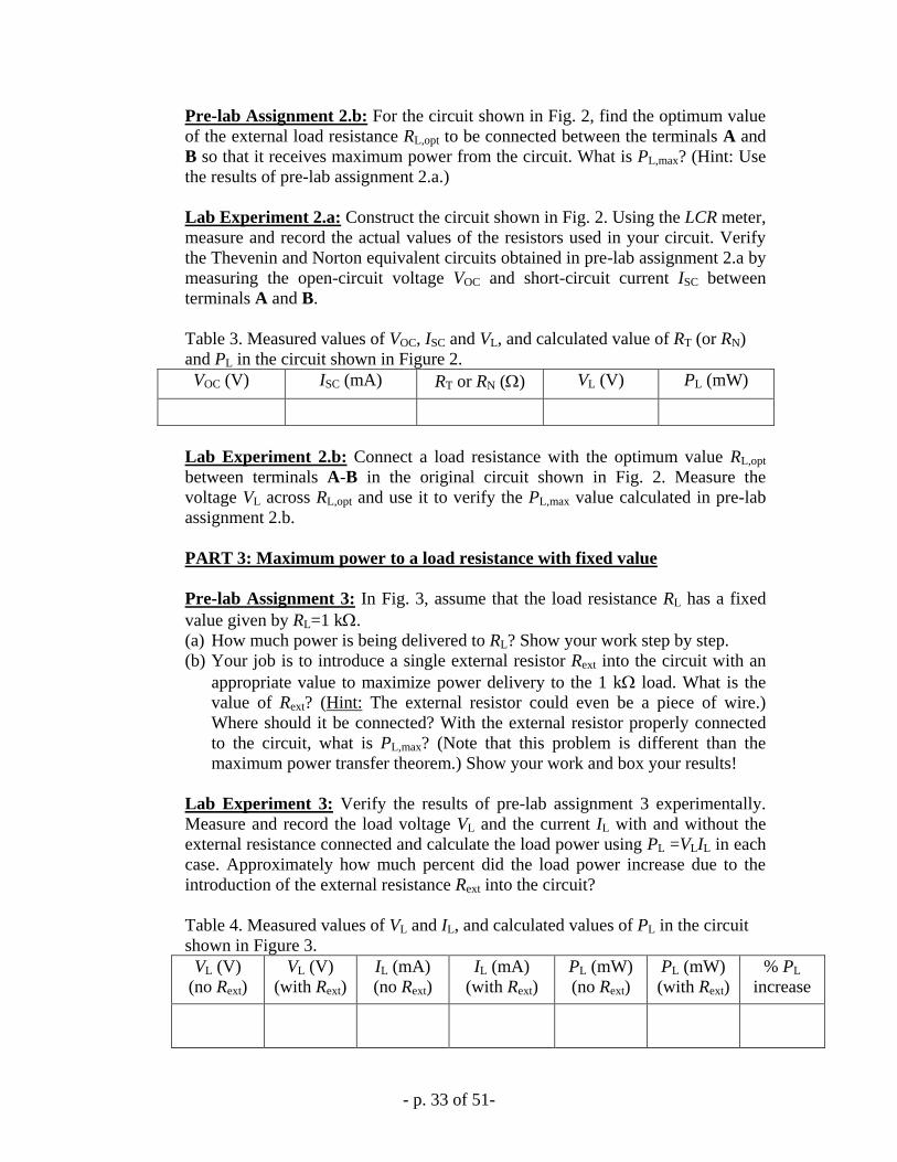
Pre-lab Assignment 2.b: For the circuit shown in Fig. 2, find the optimum value
of the external load resistance RL,opt to be connected between the terminals A and
B so that it receives maximum power from the circuit. What is PL,max? (Hint: Use
the results of pre-lab assignment 2.a.)
Lab Experiment 2.a: Construct the circuit shown in Fig. 2. Using the LCR meter,
measure and record the actual values of the resistors used in your circuit. Verify
the Thevenin and Norton equivalent circuits obtained in pre-lab assignment 2.a by
measuring the open-circuit voltage VOC and short-circuit current ISC between
terminals A and B.
Table 3. Measured values of VOC, ISC and VL, and calculated value of RT (or RN)
and PL in the circuit shown in Figure 2.
VOC (V) ISC (mA) RT or RN () VL (V) PL (mW)
Lab Experiment 2.b: Connect a load resistance with the optimum value RL,opt
between terminals A-B in the original circuit shown in Fig. 2. Measure the
voltage VL across RL,opt and use it to verify the PL,max value calculated in pre-lab
assignment 2.b.
PART 3: Maximum power to a load resistance with fixed value
Pre-lab Assignment 3: In Fig. 3, assume that the load resistance RL has a fixed
value given by RL=1 k.
(a) How much power is being delivered to RL? Show your work step by step.
(b) Your job is to introduce a single external resistor Rext into the circuit with an
appropriate value to maximize power delivery to the 1 k load. What is the
value of Rext? (Hint: The external resistor could even be a piece of wire.)
Where should it be connected? With the external resistor properly connected
to the circuit, what is PL,max? (Note that this problem is different than the
maximum power transfer theorem.) Show your work and box your results!
Lab Experiment 3: Verify the results of pre-lab assignment 3 experimentally.
Measure and record the load voltage VL and the current IL with and without the
external resistance connected and calculate the load power using PL =VLIL in each
case. Approximately how much percent did the load power increase due to the
introduction of the external resistance Rext into the circuit?
Table 4. Measured values of VL and IL, and calculated values of PL in the circuit
shown in Figure 3.
VL (V)
(no Rext)
VL (V)
(with Rext)
IL (mA)
(no Rext)
IL (mA)
(with Rext)
PL (mW)
(no Rext)
PL (mW)
(with Rext)
% PL
increase
- p. 34 of 51-
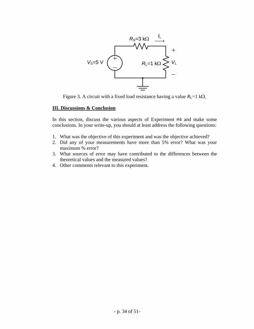
VS=5 V
RS=3 k
RL=1 k VL
IL
Figure 3. A circuit with a fixed load resistance having a value RL=1 k.
III. Discussions & Conclusion
In this section, discuss the various aspects of Experiment #4 and make some
conclusions. In your write-up, you should at least address the following questions:
1. What was the objective of this experiment and was the objective achieved?
2. Did any of your measurements have more than 5% error? What was your
maximum % error?
3. What sources of error may have contributed to the differences between the
theoretical values and the measured values?
4. Other comments relevant to this experiment.
- p. 35 of 51-
University f Prtland
Schl f Engineering
EE 271Electrical Circuits Laboratory
Lab Experiment #5: DAC R-2R
Ladder Network
- p. 36 of 51-
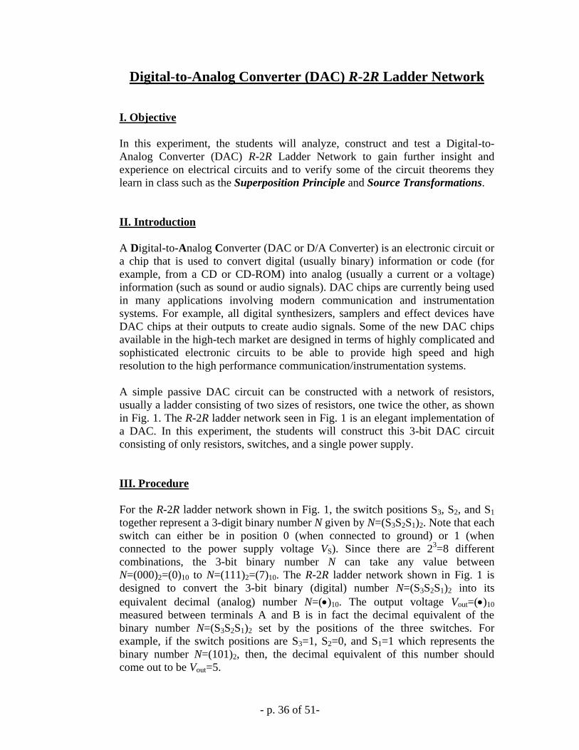
Digital-to-Analog Converter (DAC) R-2R Ladder Network
I. Objective
In this experiment, the students will analyze, construct and test a Digital-to-
Analog Converter (DAC) R-2R Ladder Network to gain further insight and
experience on electrical circuits and to verify some of the circuit theorems they
learn in class such as the Superposition Principle and Source Transformations.
II. Introduction
A Digital-to-Analog Converter (DAC or D/A Converter) is an electronic circuit or
a chip that is used to convert digital (usually binary) information or code (for
example, from a CD or CD-ROM) into analog (usually a current or a voltage)
information (such as sound or audio signals). DAC chips are currently being used
in many applications involving modern communication and instrumentation
systems. For example, all digital synthesizers, samplers and effect devices have
DAC chips at their outputs to create audio signals. Some of the new DAC chips
available in the high-tech market are designed in terms of highly complicated and
sophisticated electronic circuits to be able to provide high speed and high
resolution to the high performance communication/instrumentation systems.
A simple passive DAC circuit can be constructed with a network of resistors,
usually a ladder consisting of two sizes of resistors, one twice the other, as shown
in Fig. 1. The R-2R ladder network seen in Fig. 1 is an elegant implementation of
a DAC. In this experiment, the students will construct this 3-bit DAC circuit
consisting of only resistors, switches, and a single power supply.
III. Procedure
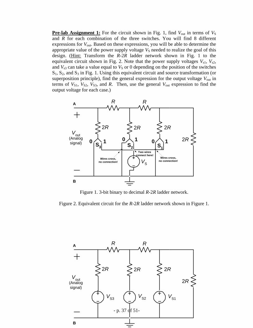
For the R-2R ladder network shown in Fig. 1, the switch positions S3, S2, and S1
together represent a 3-digit binary number N given by N=(S3S2S1)2. Note that each
switch can either be in position 0 (when connected to ground) or 1 (when
connected to the power supply voltage VS). Since there are 23=8 different
combinations, the 3-bit binary number N can take any value between
N=(000)2=(0)10 to N=(111)2=(7)10. The R-2R ladder network shown in Fig. 1 is
designed to convert the 3-bit binary (digital) number N=(S3S2S1)2 into its
equivalent decimal (analog) number N=()10. The output voltage Vout=()10
measured between terminals A and B is in fact the decimal equivalent of the
binary number N=(S3S2S1)2 set by the positions of the three switches. For
example, if the switch positions are S3=1, S2=0, and S1=1 which represents the
binary number N=(101)2, then, the decimal equivalent of this number should
come out to be Vout=5.
- p. 37 of 51-
Pre-lab Assignment 1: For the circuit shown in Fig. 1, find Vout in terms of VS
and R for each combination of the three switches. You will find 8 different
expressions for Vout. Based on these expressions, you will be able to determine the
appropriate value of the power supply voltage VS needed to realize the goal of this
design. (Hint: Transform the R-2R ladder network shown in Fig. 1 to the
equivalent circuit shown in Fig. 2. Note that the power supply voltages Vs1, Vs2,
and Vs3 can take a value equal to VS or 0 depending on the position of the switches
S1, S2, and S3 in Fig. 1. Using this equivalent circuit and source transformation (or
superposition principle), find the general expression for the output voltage Vout in
terms of VS1, VS2, VS3, and R. Then, use the general Vout expression to find the
output voltage for each case.)
Figure 1. 3-bit binary to decimal R-2R ladder network.
Figure 2. Equivalent circuit for the R-2R ladder network shown in Figure 1.
RA
B
VS
R
2R 2R 2R
2R
Vout
(Analog
signal) 0 1 0 1 0 1S
3 S2 S
1
Wires cross,
no connection!Wires cross,
no connection!
Two wires
connect here!
RA
B
VS3
R
2R 2R 2R
2RV
out(Analog
signal)
VS2 V
S1
- p. 38 of 51-
Pre-lab Assignment 2: Can you redesign the circuit shown in Fig. 1 to be able to
convert any 4-bit binary number into its decimal equivalent? If so, how many
additional elements would you need and what will be the new value of the power
supply voltage VS?
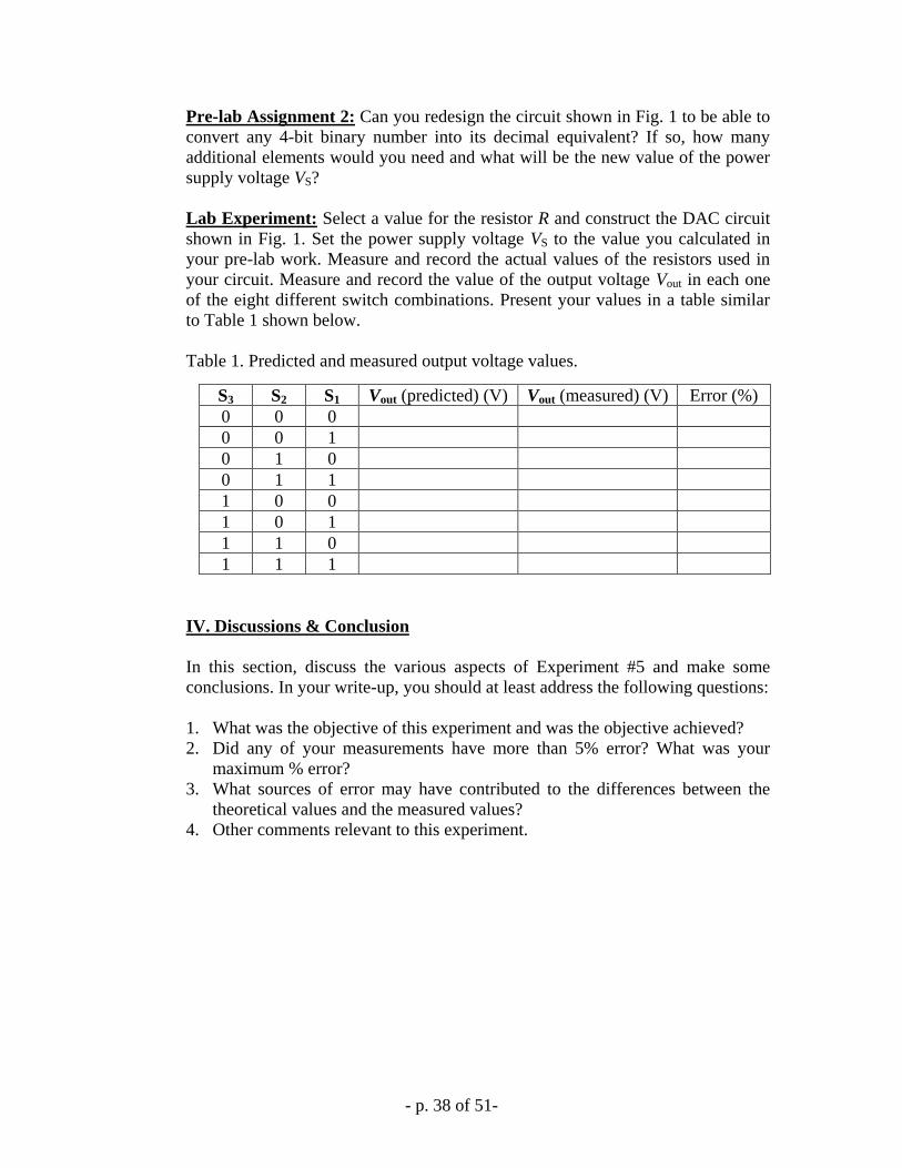
Lab Experiment: Select a value for the resistor R and construct the DAC circuit
shown in Fig. 1. Set the power supply voltage VS to the value you calculated in
your pre-lab work. Measure and record the actual values of the resistors used in
your circuit. Measure and record the value of the output voltage Vout in each one
of the eight different switch combinations. Present your values in a table similar
to Table 1 shown below.
Table 1. Predicted and measured output voltage values.
S3 S2 S1 Vout (predicted) (V) Vout (measured) (V) Error (%)
0 0 0
0 0 1
0 1 0
0 1 1
1 0 0
1 0 1
1 1 0
1 1 1
IV. Discussions & Conclusion
In this section, discuss the various aspects of Experiment #5 and make some
conclusions. In your write-up, you should at least address the following questions:
1. What was the objective of this experiment and was the objective achieved?
2. Did any of your measurements have more than 5% error? What was your
maximum % error?
3. What sources of error may have contributed to the differences between the
theoretical values and the measured values?
4. Other comments relevant to this experiment.
- p. 39 of 51-
University f Prtland
Schl f Engineering
EE 271Electrical Circuits Laboratory
Lab Experiment #7:
First-Order RC Circuits as Low-Pass and
High-Pass Filters
- p. 40 of 51-
First-Order RC Circuits as Low-Pass & High-Pass Filters
I. Objective
In this experiment, the students will make measurements and observations on the
step and sinusoidal steady-state responses of simple first-order RC circuits. They
will also understand how first-order RC circuits can be used as low-pass or high-
pass filters.
II. Procedure
PART 1: Step Excitation of First-Order RC Circuits
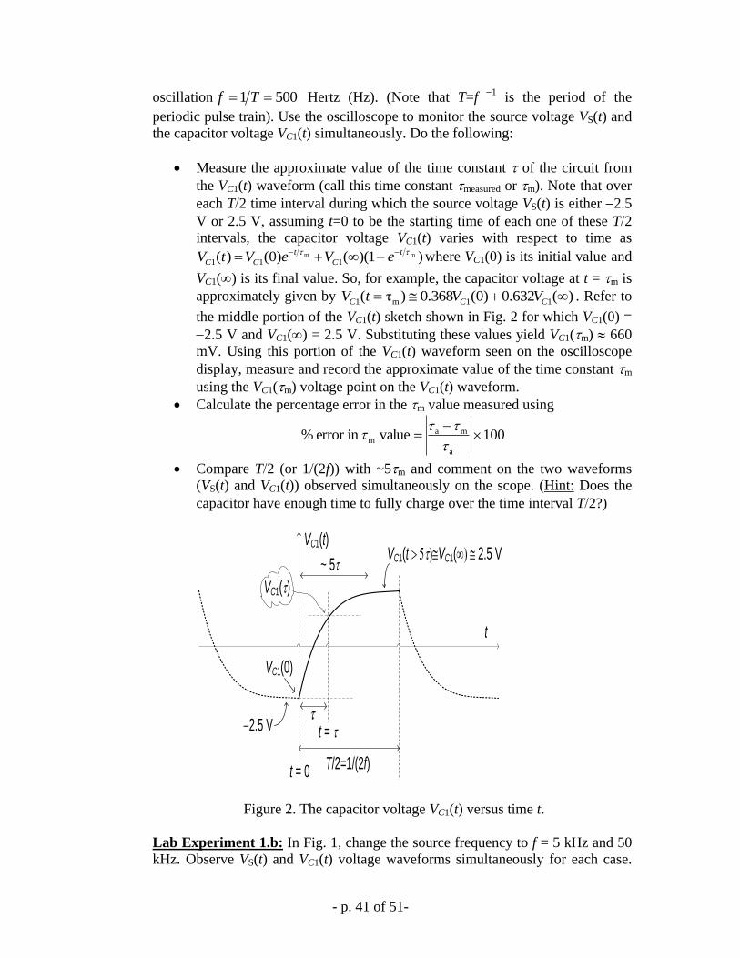
Pre-lab Assignment 1.a: A first-order capacitive circuit is excited by a periodic
rectangular pulse train as shown in Fig. 1. The element values of the circuit are
given by R1=10 k and C1=10 nF respectively. Calculate the following:
The time constant of this circuit (call this time constant pre-lab or p).
Approximate time it takes for the capacitor to fully charge or discharge.
(The time for the capacitor to fully charge or discharge corresponds to the
time it takes for the capacitor voltage to reach approximately 99% of its
final value.)
VC1VS
R1=
10 k
C1=
10 nF
2.5 V
2.5 V
Scope
Channel 2
Output
Signal
Scope
Channel 1
Input
Signal
LPF
Figure 1. First-order RC circuit connected like a Low-Pass Filter (LPF).
Lab Experiment 1.a: Construct the first-order RC circuit shown in Fig. 1 using
R1=10 k and C1=10 nF. Using the digital LCR meter, measure and record the
actual values of the resistor and the capacitor used in your circuit. Use these
actual element values measured to recalculate the time constant (call this time
constant actual or a). Use the function generator available on your bench to supply
the periodic rectangular pulse train to the circuit. Set the function generator to
provide the rectangular pulse train represented with source voltage VS(t) which
oscillates between 2.5 V and 2.5 V (i.e., 5 V peak-to-peak) with frequency of
- p. 41 of 51-
oscillation 5001 Tf Hertz (Hz). (Note that T=f 1
is the period of the
periodic pulse train). Use the oscilloscope to monitor the source voltage VS(t) and
the capacitor voltage VC1(t) simultaneously. Do the following:
Measure the approximate value of the time constant of the circuit from
the VC1(t) waveform (call this time constant measured or m). Note that over
each T2 time interval during which the source voltage VS(t) is either 2.5
V or 2.5 V, assuming t=0 to be the starting time of each one of these T2
intervals, the capacitor voltage VC1(t) varies with respect to time as
)1)(()0()( mm
111
t
C
t
CC eVeVtV
where VC1(0) is its initial value and
VC1() is its final value. So, for example, the capacitor voltage at t = m is
approximately given by )(632.0)0(368.0)τ( 11m1 CCC VVtV . Refer to
the middle portion of the VC1(t) sketch shown in Fig. 2 for which VC1(0) =
2.5 V and VC1() = 2.5 V. Substituting these values yield VC1(m) 660
mV. Using this portion of the VC1(t) waveform seen on the oscilloscope
display, measure and record the approximate value of the time constant m
using the VC1(m) voltage point on the VC1(t) waveform.
Calculate the percentage error in the m value measured using
100 value inerror %a
mam
Compare T2 (or 1(2f)) with ~5m and comment on the two waveforms
(VS(t) and VC1(t)) observed simultaneously on the scope. (Hint: Does the
capacitor have enough time to fully charge over the time interval T2?)
2.5 V
VC1(t > 5VC1( 2.5 V
VC1(0)
t = 0
t =
VC1()
t
VC1(t)
T/2=1/(2f)
~ 5
Figure 2. The capacitor voltage VC1(t) versus time t.
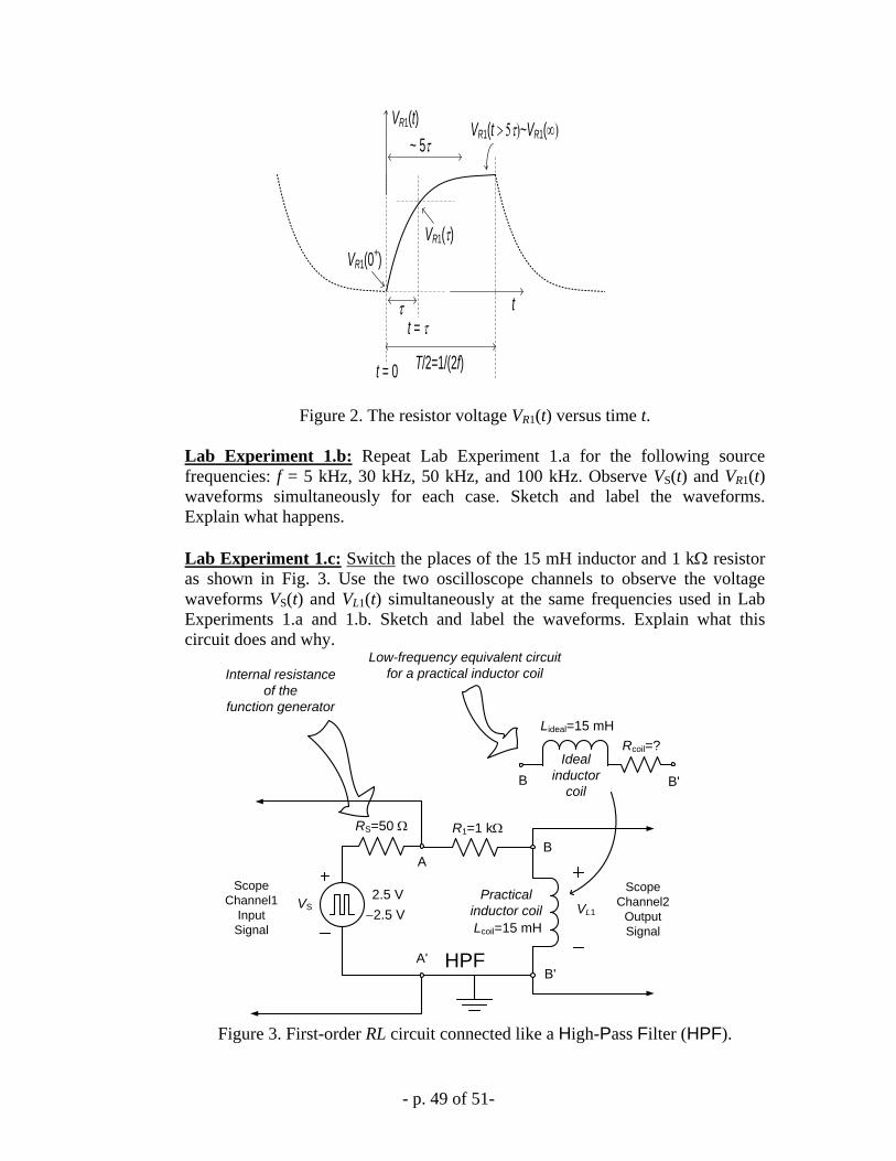
Lab Experiment 1.b: In Fig. 1, change the source frequency to f = 5 kHz and 50
kHz. Observe VS(t) and VC1(t) voltage waveforms simultaneously for each case.
- p. 42 of 51-
Sketch and label the waveforms. Based on your observations, explain what
happens and why this circuit is referred to as a Low-Pass Filter (LPF).
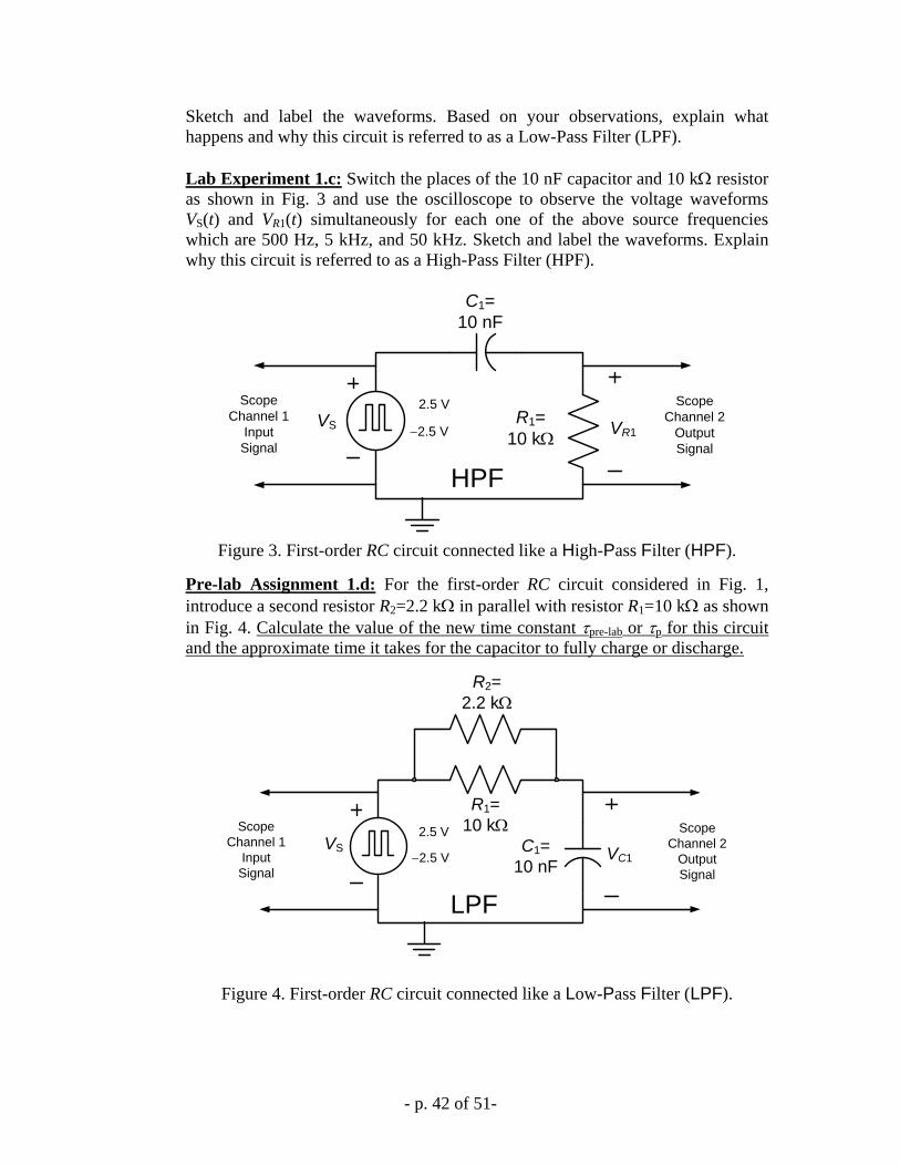
Lab Experiment 1.c: Switch the places of the 10 nF capacitor and 10 k resistor
as shown in Fig. 3 and use the oscilloscope to observe the voltage waveforms
VS(t) and VR1(t) simultaneously for each one of the above source frequencies
which are 500 Hz, 5 kHz, and 50 kHz. Sketch and label the waveforms. Explain
why this circuit is referred to as a High-Pass Filter (HPF).
VR1VS
C1=
10 nF
R1=
10 k
2.5 V
2.5 V
Scope
Channel 1
Input
Signal
Scope
Channel 2
Output
Signal
HPF
Figure 3. First-order RC circuit connected like a High-Pass Filter (HPF).
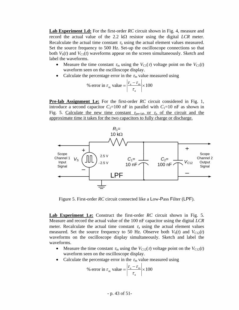
Pre-lab Assignment 1.d: For the first-order RC circuit considered in Fig. 1,
introduce a second resistor R2=2.2 k in parallel with resistor R1=10 k as shown
in Fig. 4. Calculate the value of the new time constant pre-lab or p for this circuit
and the approximate time it takes for the capacitor to fully charge or discharge.
VC1VS
R1=
10 k
C1=
10 nF
R2=
2.2 k
2.5 V
2.5 V
Scope
Channel 2
Output
Signal
Scope
Channel 1
Input
Signal
LPF
Figure 4. First-order RC circuit connected like a Low-Pass Filter (LPF).
- p. 43 of 51-
Lab Experiment 1.d: For the first-order RC circuit shown in Fig. 4, measure and
record the actual value of the 2.2 k resistor using the digital LCR meter.
Recalculate the actual time constant a using the actual element values measured.
Set the source frequency to 500 Hz. Set-up the oscilloscope connections so that
both VS(t) and VC1(t) waveforms appear on the screen simultaneously. Sketch and
label the waveforms.
Measure the time constant m using the VC1() voltage point on the VC1(t)
waveform seen on the oscilloscope display.
Calculate the percentage error in the m value measured using
100 value inerror %a
mam
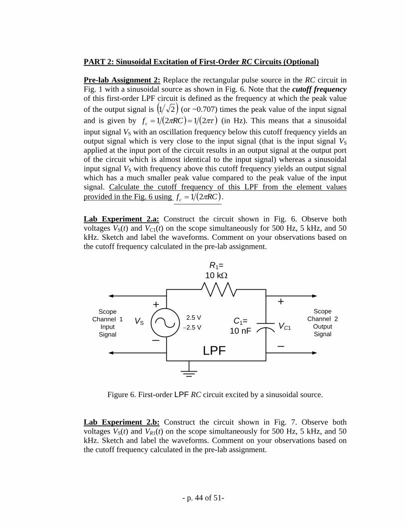
Pre-lab Assignment 1.e: For the first-order RC circuit considered in Fig. 1,
introduce a second capacitor C2=100 nF in parallel with C1=10 nF as shown in
Fig. 5. Calculate the new time constant pre-lab or p of the circuit and the
approximate time it takes for the two capacitors to fully charge or discharge.
Scope
Channel 2
Output
Signal
VC12VS
R1=
10 k
C1=
10 nF
C2=
100 nF
2.5 V
2.5 V
Scope
Channel 1
Input
Signal
LPF
Figure 5. First-order RC circuit connected like a Low-Pass Filter (LPF).
Lab Experiment 1.e: Construct the first-order RC circuit shown in Fig. 5.
Measure and record the actual value of the 100 nF capacitor using the digital LCR
meter. Recalculate the actual time constant a using the actual element values
measured. Set the source frequency to 50 Hz. Observe both VS(t) and VC12(t)
waveforms on the oscilloscope display simultaneously. Sketch and label the
waveforms.
Measure the time constant m using the VC12() voltage point on the VC12(t)
waveform seen on the oscilloscope display.
Calculate the percentage error in the m value measured using
100 value inerror %a
mam
- p. 44 of 51-
PART 2: Sinusoidal Excitation of First-Order RC Circuits (Optional)
Pre-lab Assignment 2: Replace the rectangular pulse source in the RC circuit in
Fig. 1 with a sinusoidal source as shown in Fig. 6. Note that the cutoff frequency
of this first-order LPF circuit is defined as the frequency at which the peak value
of the output signal is 21 (or ~0.707) times the peak value of the input signal
and is given by 2121 RCfc (in Hz). This means that a sinusoidal
input signal VS with an oscillation frequency below this cutoff frequency yields an
output signal which is very close to the input signal (that is the input signal VS
applied at the input port of the circuit results in an output signal at the output port
of the circuit which is almost identical to the input signal) whereas a sinusoidal
input signal VS with frequency above this cutoff frequency yields an output signal
which has a much smaller peak value compared to the peak value of the input
signal. Calculate the cutoff frequency of this LPF from the element values
provided in the Fig. 6 using RCfc 21 .
Lab Experiment 2.a: Construct the circuit shown in Fig. 6. Observe both
voltages VS(t) and VC1(t) on the scope simultaneously for 500 Hz, 5 kHz, and 50
kHz. Sketch and label the waveforms. Comment on your observations based on
the cutoff frequency calculated in the pre-lab assignment.
VC1VS
R1=
10 k
C1=
10 nF
2.5 V
2.5 V
Scope
Channel 2
Output
Signal
Scope
Channel 1
Input
Signal
LPF
Figure 6. First-order LPF RC circuit excited by a sinusoidal source.
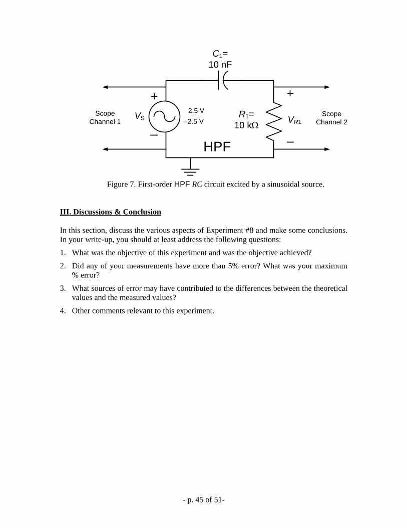
Lab Experiment 2.b: Construct the circuit shown in Fig. 7. Observe both
voltages VS(t) and VR1(t) on the scope simultaneously for 500 Hz, 5 kHz, and 50
kHz. Sketch and label the waveforms. Comment on your observations based on
the cutoff frequency calculated in the pre-lab assignment.
- p. 45 of 51-
VR1VS
C1=
10 nF
R1=
10 k
2.5 V
2.5 VScope
Channel 1Scope
Channel 2
HPF
Figure 7. First-order HPF RC circuit excited by a sinusoidal source.
III. Discussions & Conclusion
In this section, discuss the various aspects of Experiment #8 and make some conclusions.
In your write-up, you should at least address the following questions:
1. What was the objective of this experiment and was the objective achieved?
2. Did any of your measurements have more than 5% error? What was your maximum
% error?
3. What sources of error may have contributed to the differences between the theoretical
values and the measured values?
4. Other comments relevant to this experiment.
- p. 46 of 51-
University f Prtland
Schl f Engineering
EE 271Electrical Circuits Laboratory
Lab Experiment #8:
Transient Response of First-Order RL
and Second-Order RLC Circuits
- p. 47 of 51-
Transient Response of First-Order RL and
Second-Order RLC Circuits
I. Objective
In this experiment, the students will make measurements and observations on the
transient step response of simple RL and RLC circuits.
II. Procedure
PART 1: Step Excitation of First-Order RL Circuits
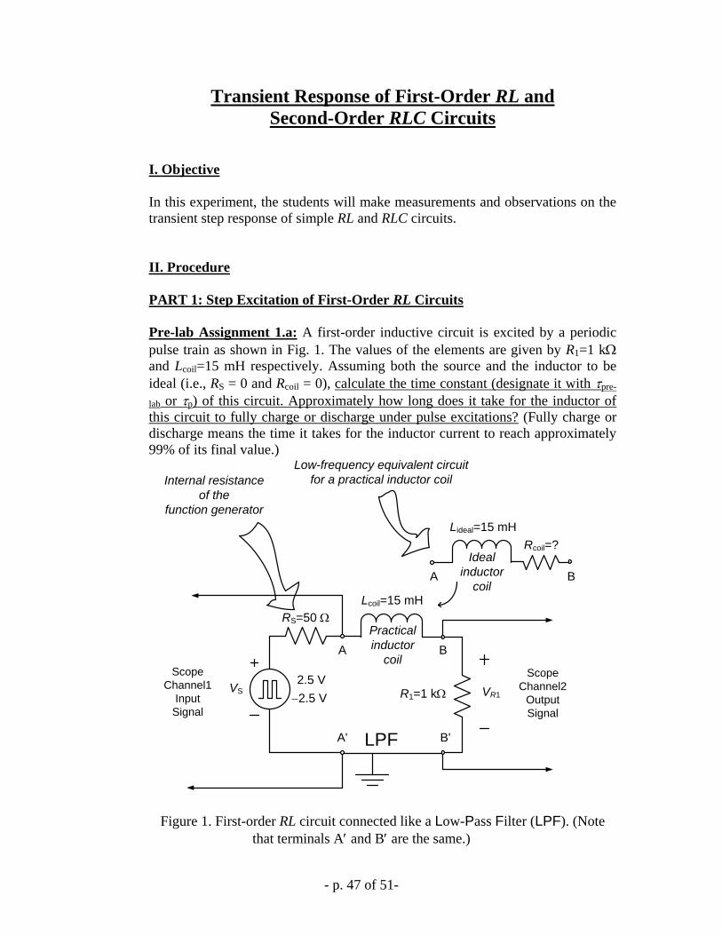
Pre-lab Assignment 1.a: A first-order inductive circuit is excited by a periodic
pulse train as shown in Fig. 1. The values of the elements are given by R1=1 k
and Lcoil=15 mH respectively. Assuming both the source and the inductor to be
ideal (i.e., RS = 0 and Rcoil = 0), calculate the time constant (designate it with pre-
lab or p) of this circuit. Approximately how long does it take for the inductor of
this circuit to fully charge or discharge under pulse excitations? (Fully charge or
discharge means the time it takes for the inductor current to reach approximately
99% of its final value.)
VR1
2.5 V
2.5 VVS
Scope
Channel2
Output
Signal
Scope
Channel1
Input
Signal
R1=1 k
LPF
Lcoil=15 mH
Practical
inductor
coil
Ideal
inductor
coil
Rcoil=?
Lideal=15 mH
Low-frequency equivalent circuit
for a practical inductor coil
RS=50
A B
A B
Internal resistance
of the
function generator
A' B'
Figure 1. First-order RL circuit connected like a Low-Pass Filter (LPF). (Note
that terminals A and B are the same.)
- p. 48 of 51-
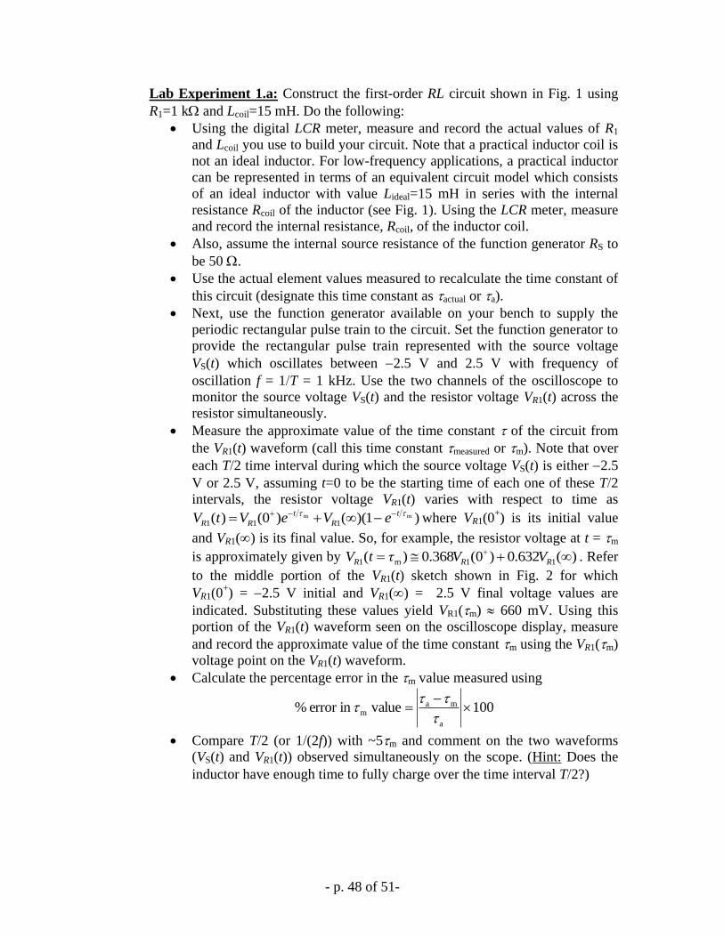
Lab Experiment 1.a: Construct the first-order RL circuit shown in Fig. 1 using
R1=1 k and Lcoil=15 mH. Do the following:
Using the digital LCR meter, measure and record the actual values of R1
and Lcoil you use to build your circuit. Note that a practical inductor coil is
not an ideal inductor. For low-frequency applications, a practical inductor
can be represented in terms of an equivalent circuit model which consists
of an ideal inductor with value Lideal=15 mH in series with the internal
resistance Rcoil of the inductor (see Fig. 1). Using the LCR meter, measure
and record the internal resistance, Rcoil, of the inductor coil.
Also, assume the internal source resistance of the function generator RS to
be 50 .
Use the actual element values measured to recalculate the time constant of
this circuit (designate this time constant as actual or a).
Next, use the function generator available on your bench to supply the
periodic rectangular pulse train to the circuit. Set the function generator to
provide the rectangular pulse train represented with the source voltage
VS(t) which oscillates between 2.5 V and 2.5 V with frequency of
oscillation f = 1T = 1 kHz. Use the two channels of the oscilloscope to
monitor the source voltage VS(t) and the resistor voltage VR1(t) across the
resistor simultaneously.
Measure the approximate value of the time constant of the circuit from
the VR1(t) waveform (call this time constant measured or m). Note that over
each T2 time interval during which the source voltage VS(t) is either 2.5
V or 2.5 V, assuming t=0 to be the starting time of each one of these T2
intervals, the resistor voltage VR1(t) varies with respect to time as
)1)(()0()( mm
111
t
R
t
RR eVeVtV where VR1(0
+) is its initial value
and VR1() is its final value. So, for example, the resistor voltage at t = m
is approximately given by )(632.0)0(368.0)( 11m1
RRR VVτtV . Refer
to the middle portion of the VR1(t) sketch shown in Fig. 2 for which
VR1(0+) = 2.5 V initial and VR1() = 2.5 V final voltage values are
indicated. Substituting these values yield VR1(m) 660 mV. Using this
portion of the VR1(t) waveform seen on the oscilloscope display, measure
and record the approximate value of the time constant m using the VR1(m)
voltage point on the VR1(t) waveform.
Calculate the percentage error in the m value measured using
100 value inerror %a
mam
Compare T2 (or 1(2f)) with ~5m and comment on the two waveforms
(VS(t) and VR1(t)) observed simultaneously on the scope. (Hint: Does the
inductor have enough time to fully charge over the time interval T2?)
- p. 49 of 51-
VR1(t > 5~VR1(
VR1(0+)
t = 0
t =
VR1()
t
VR1(t)
T/2=1/(2f)
~ 5
Figure 2. The resistor voltage VR1(t) versus time t.
Lab Experiment 1.b: Repeat Lab Experiment 1.a for the following source
frequencies: f = 5 kHz, 30 kHz, 50 kHz, and 100 kHz. Observe VS(t) and VR1(t)
waveforms simultaneously for each case. Sketch and label the waveforms.
Explain what happens.
Lab Experiment 1.c: Switch the places of the 15 mH inductor and 1 k resistor
as shown in Fig. 3. Use the two oscilloscope channels to observe the voltage
waveforms VS(t) and VL1(t) simultaneously at the same frequencies used in Lab
Experiments 1.a and 1.b. Sketch and label the waveforms. Explain what this
circuit does and why.
VL1
2.5 V
2.5 VVS
Scope
Channel2
Output
Signal
Scope
Channel1
Input
Signal
R1=1 k
HPF
Lcoil=15 mH
Practical
inductor coil
Ideal
inductor
coil
Rcoil=?
Lideal=15 mH
Low-frequency equivalent circuit
for a practical inductor coil
RS=50
AB
B
Internal resistance
of the
function generator
A'B'
B'
Figure 3. First-order RL circuit connected like a High-Pass Filter (HPF).
- p. 50 of 51-
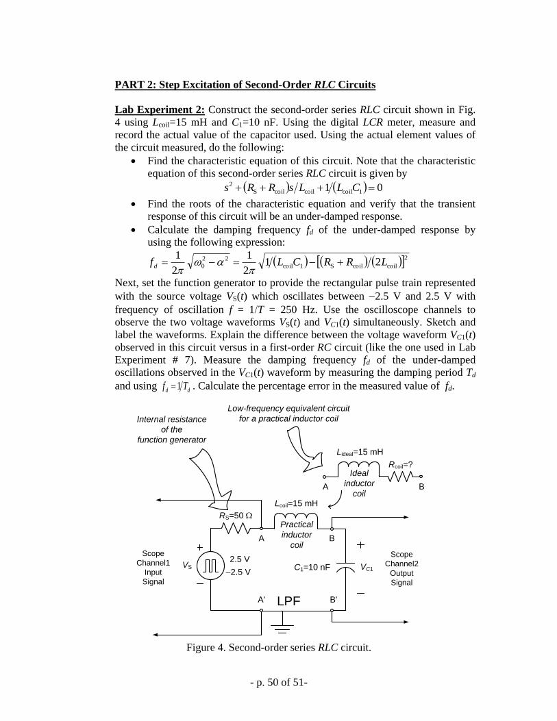
PART 2: Step Excitation of Second-Order RLC Circuits
Lab Experiment 2: Construct the second-order series RLC circuit shown in Fig.
4 using Lcoil=15 mH and C1=10 nF. Using the digital LCR meter, measure and
record the actual value of the capacitor used. Using the actual element values of
the circuit measured, do the following:
Find the characteristic equation of this circuit. Note that the characteristic
equation of this second-order series RLC circuit is given by
01 1coilcoilcoilS
2 CLLsRRs
Find the roots of the characteristic equation and verify that the transient
response of this circuit will be an under-damped response.
Calculate the damping frequency fd of the under-damped response by
using the following expression:
2
coilcoilS1coil
22
0 212
1
2
1LRRCLfd
Next, set the function generator to provide the rectangular pulse train represented
with the source voltage VS(t) which oscillates between 2.5 V and 2.5 V with
frequency of oscillation f = 1T = 250 Hz. Use the oscilloscope channels to
observe the two voltage waveforms VS(t) and VC1(t) simultaneously. Sketch and
label the waveforms. Explain the difference between the voltage waveform VC1(t)
observed in this circuit versus in a first-order RC circuit (like the one used in Lab
Experiment # 7). Measure the damping frequency fd of the under-damped
oscillations observed in the VC1(t) waveform by measuring the damping period Td
and using dd Tf 1 . Calculate the percentage error in the measured value of fd.
2.5 V
2.5 VVS
Scope
Channel2
Output
Signal
Scope
Channel1
Input
Signal
LPF
Lcoil=15 mH
Practical
inductor
coil
Ideal
inductor
coil
Rcoil=?
Lideal=15 mH
Low-frequency equivalent circuit
for a practical inductor coil
RS=50
A B
A B
Internal resistance
of the
function generator
A' B'
C1=10 nF VC1
Figure 4. Second-order series RLC circuit.
- p. 51 of 51-
Repeat this experiment at 5 kHz, 10 kHz, and 20 kHz and observe the two voltage
waveforms on the oscilloscope simultaneously in each case. Sketch and label the
waveforms. Provide an explanation as to what happens to the two waveforms as
the source frequency increases.
III. Discussions & Conclusion
In this section, discuss the various aspects of Experiment # 8 and state some conclusions.
In your write-up, you should at least address the following questions:
1. What was the objective of this experiment and was the objective achieved?
2. Explain how the output resistance of the function generator affected some of the
waveforms observed on the scope and why. Why was this effect not observed in
the first-order RC experiment (i.e., Experiment # 7)?
3. Did any of your measurements have more than 5% error? What was your
maximum % error?
4. What sources of error may have contributed to the differences between the
theoretical values and the measured values?
5. Other comments relevant to this experiment.
- p. 52 of 51-
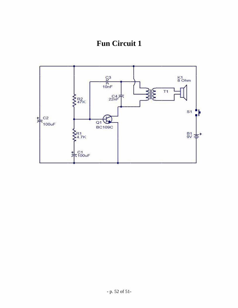
Fun Circuit 1
- p. 53 of 51-
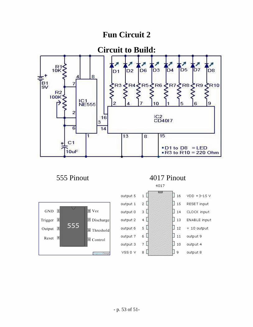
Fun Circuit 2
Circuit to Build:
555 Pinout 4017 Pinout
- p. 54 of 51-
- p. 55 of 51-
Fun Circuit 3
The following is an excerpt of a lab from:
Worcester Polytechnic Institute
Department of Electrical and Computer Engineering
ECE3601 – Intro to Electrical Engineering
Laboratory Project 5: Operational amplifier I
- 11 -
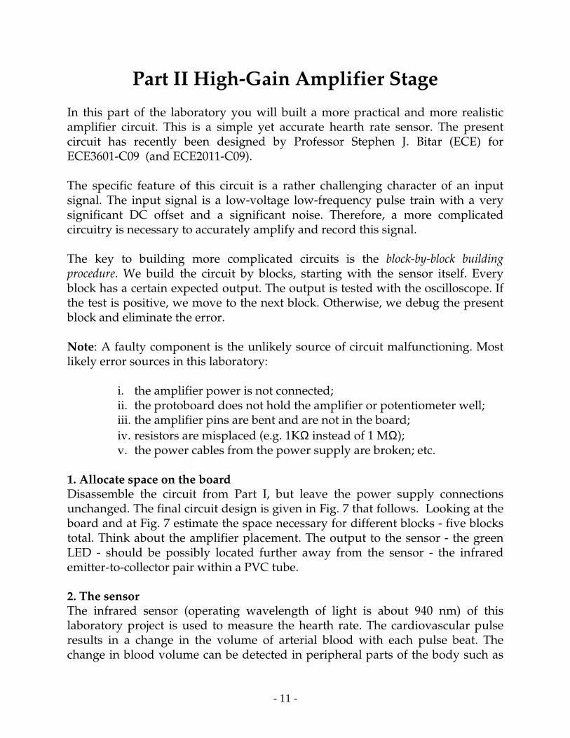
Part II High-Gain Amplifier Stage
In this part of the laboratory you will built a more practical and more realistic amplifier circuit. This is a simple yet accurate hearth rate sensor. The present circuit has recently been designed by Professor Stephen J. Bitar (ECE) for ECE3601-C09 (and ECE2011-C09). The specific feature of this circuit is a rather challenging character of an input signal. The input signal is a low-voltage low-frequency pulse train with a very significant DC offset and a significant noise. Therefore, a more complicated circuitry is necessary to accurately amplify and record this signal. The key to building more complicated circuits is the block-by-block building procedure. We build the circuit by blocks, starting with the sensor itself. Every block has a certain expected output. The output is tested with the oscilloscope. If the test is positive, we move to the next block. Otherwise, we debug the present block and eliminate the error. Note: A faulty component is the unlikely source of circuit malfunctioning. Most likely error sources in this laboratory:
i. the amplifier power is not connected; ii. the protoboard does not hold the amplifier or potentiometer well; iii. the amplifier pins are bent and are not in the board;
iv. resistors are misplaced (e.g. 1KΩ instead of 1 MΩ); v. the power cables from the power supply are broken; etc.
1. Allocate space on the board Disassemble the circuit from Part I, but leave the power supply connections unchanged. The final circuit design is given in Fig. 7 that follows. Looking at the board and at Fig. 7 estimate the space necessary for different blocks - five blocks total. Think about the amplifier placement. The output to the sensor - the green LED - should be possibly located further away from the sensor - the infrared emitter-to-collector pair within a PVC tube. 2. The sensor The infrared sensor (operating wavelength of light is about 940 nm) of this laboratory project is used to measure the hearth rate. The cardiovascular pulse results in a change in the volume of arterial blood with each pulse beat. The change in blood volume can be detected in peripheral parts of the body such as
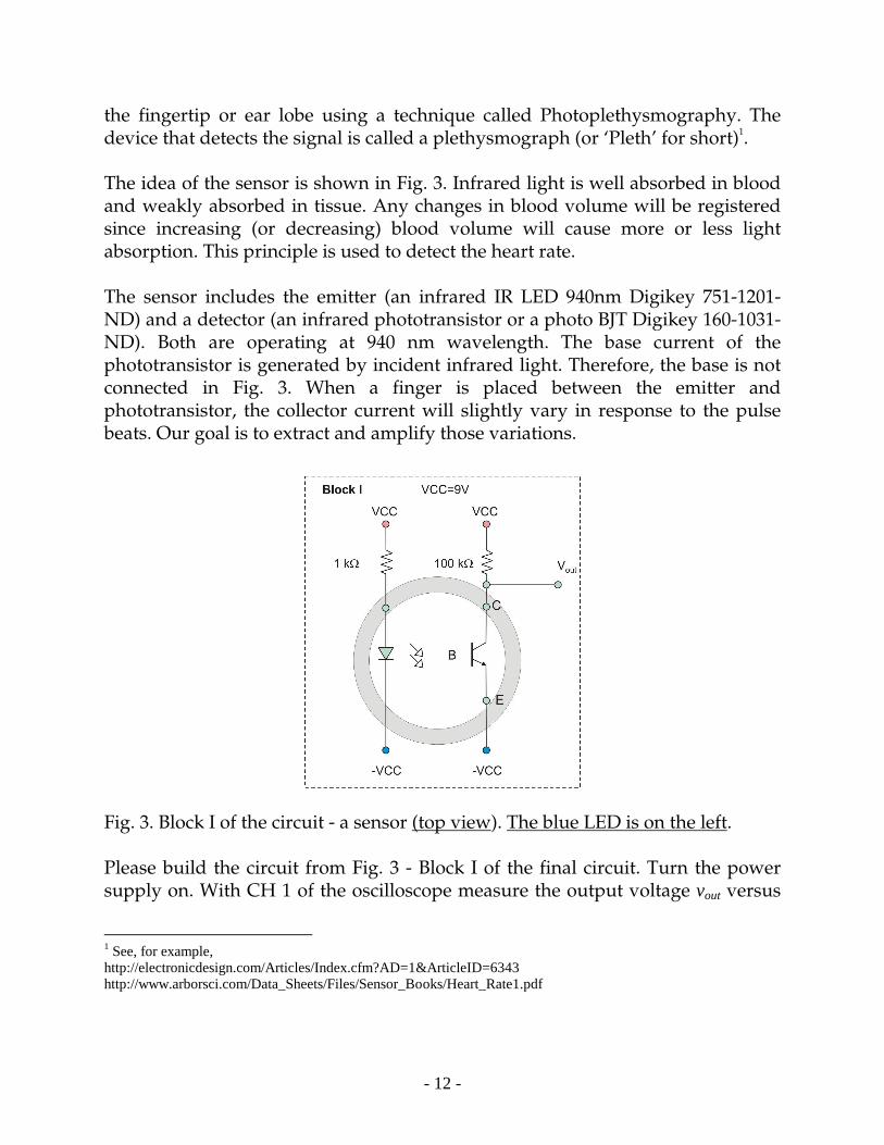
- 12 -
the fingertip or ear lobe using a technique called Photoplethysmography. The device that detects the signal is called a plethysmograph (or ‘Pleth’ for short)1. The idea of the sensor is shown in Fig. 3. Infrared light is well absorbed in blood and weakly absorbed in tissue. Any changes in blood volume will be registered since increasing (or decreasing) blood volume will cause more or less light absorption. This principle is used to detect the heart rate. The sensor includes the emitter (an infrared IR LED 940nm Digikey 751-1201-ND) and a detector (an infrared phototransistor or a photo BJT Digikey 160-1031-ND). Both are operating at 940 nm wavelength. The base current of the phototransistor is generated by incident infrared light. Therefore, the base is not connected in Fig. 3. When a finger is placed between the emitter and phototransistor, the collector current will slightly vary in response to the pulse beats. Our goal is to extract and amplify those variations.
Fig. 3. Block I of the circuit - a sensor (top view). The blue LED is on the left. Please build the circuit from Fig. 3 - Block I of the final circuit. Turn the power supply on. With CH 1 of the oscilloscope measure the output voltage vout versus
1 See, for example, http://electronicdesign.com/Articles/Index.cfm?AD=1&ArticleID=6343 http://www.arborsci.com/Data_Sheets/Files/Sensor_Books/Heart_Rate1.pdf
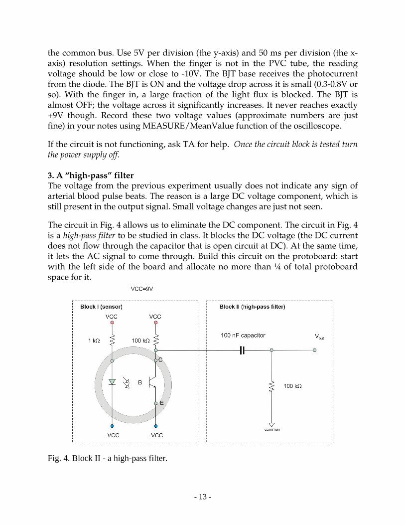
- 13 -
the common bus. Use 5V per division (the y-axis) and 50 ms per division (the x-axis) resolution settings. When the finger is not in the PVC tube, the reading voltage should be low or close to -10V. The BJT base receives the photocurrent from the diode. The BJT is ON and the voltage drop across it is small (0.3-0.8V or so). With the finger in, a large fraction of the light flux is blocked. The BJT is almost OFF; the voltage across it significantly increases. It never reaches exactly +9V though. Record these two voltage values (approximate numbers are just fine) in your notes using MEASURE/MeanValue function of the oscilloscope.
If the circuit is not functioning, ask TA for help. Once the circuit block is tested turn the power supply off. 3. A “high-pass” filter The voltage from the previous experiment usually does not indicate any sign of arterial blood pulse beats. The reason is a large DC voltage component, which is still present in the output signal. Small voltage changes are just not seen.
The circuit in Fig. 4 allows us to eliminate the DC component. The circuit in Fig. 4 is a high-pass filter to be studied in class. It blocks the DC voltage (the DC current does not flow through the capacitor that is open circuit at DC). At the same time, it lets the AC signal to come through. Build this circuit on the protoboard: start with the left side of the board and allocate no more than ¼ of total protoboard space for it.
Fig. 4. Block II - a high-pass filter.
- 14 -
The present capacitor (the tantalum capacitor) is not the electrolytic one: the polarity does not matter. The high-pass filter in this circuit has only one function: it eliminates a DC voltage offset from the voltage tVou . Only a pure AC signal
ideally passes through it. Turn power supply on. With CH 1 of the oscilloscope measure the output voltage versus the common port after the second block. Use 50mV per division (the y-axis) and 500 ms per division (the x-axis) resolution settings. When the finger is in the PVC tube, the reading voltage should be close to zero. It should have small but usually visible noisy beats corresponding to the heart rate. If this is not the case, ask TA for help. Once Block II is tested turn the power supply off. 4. Amplification After the sensor output is conditioned with the high-pass filer, we should amplify it. To do so, a non-inverting amplifier shown in Fig. 5 is employed. Please build the corresponding block (Block III). Turn the power supply on. With CH 1 of the oscilloscope we still measure the input voltage to the amplifier (output voltage of Block II) versus the common port. Use 50mV per division (the y-axis) and 500 ms per division (the x-axis) resolution settings. With CH 2 of the oscilloscope we now measure the output voltage to the amplifier (output voltage of Block III) versus the common port. Use 1V per division (the y-axis) and 500 ms per division (the x-axis) resolution settings for CH 2. The strong amplification of the input voltage signal should be observed. If this is not the case, ask TA for help. Once the circuit block is tested turn the power supply off. 5. A potential problem with the high-gain amplifier A potential problem with the high-gain amplifier in Fig. 5 is the input offset voltage. This voltage appears internally, even if the input voltage to terminals + and - is exactly zero Volts. It is an internal property of the real amplifier chip. For
LM1458, the input offset voltage may have any value between ±1 mV and ±6 mV. The offset voltage is also amplified, along with useful signal. If the amplifier has a high gain, the corresponding DC offset at the output may be quite large. This DC offset voltage at the output (with no finger in the sensor) should be observed in the previous experiment and should be recorded in your notes (an approximate value is fine). To solve this problem we introduce one more circuit block (Block IV) shown in Fig. 6.
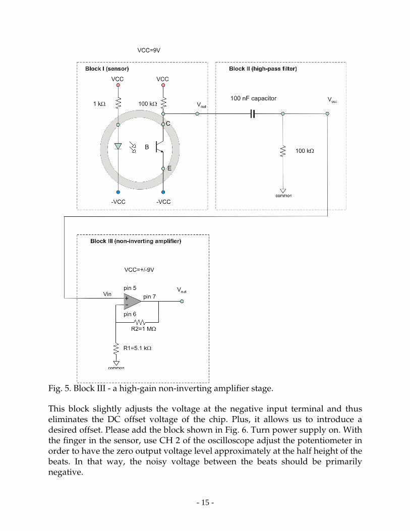
- 15 -
Fig. 5. Block III - a high-gain non-inverting amplifier stage. This block slightly adjusts the voltage at the negative input terminal and thus eliminates the DC offset voltage of the chip. Plus, it allows us to introduce a desired offset. Please add the block shown in Fig. 6. Turn power supply on. With the finger in the sensor, use CH 2 of the oscilloscope adjust the potentiometer in order to have the zero output voltage level approximately at the half height of the beats. In that way, the noisy voltage between the beats should be primarily negative.
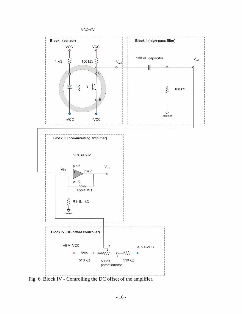
- 16 -
Fig. 6. Block IV - Controlling the DC offset of the amplifier.
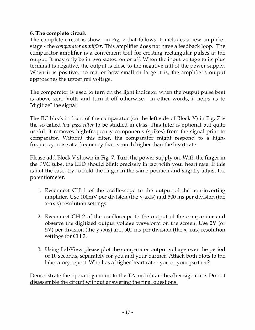
- 17 -
6. The complete circuit The complete circuit is shown in Fig. 7 that follows. It includes a new amplifier stage - the comparator amplifier. This amplifier does not have a feedback loop. The comparator amplifier is a convenient tool for creating rectangular pulses at the output. It may only be in two states: on or off. When the input voltage to its plus terminal is negative, the output is close to the negative rail of the power supply. When it is positive, no matter how small or large it is, the amplifier's output approaches the upper rail voltage. The comparator is used to turn on the light indicator when the output pulse beat is above zero Volts and turn it off otherwise. In other words, it helps us to "digitize" the signal. The RC block in front of the comparator (on the left side of Block V) in Fig. 7 is the so called low-pass filter to be studied in class. This filter is optional but quite useful: it removes high-frequency components (spikes) from the signal prior to comparator. Without this filter, the comparator might respond to a high-frequency noise at a frequency that is much higher than the heart rate. Please add Block V shown in Fig. 7. Turn the power supply on. With the finger in the PVC tube, the LED should blink precisely in tact with your heart rate. If this is not the case, try to hold the finger in the same position and slightly adjust the potentiometer.
1. Reconnect CH 1 of the oscilloscope to the output of the non-inverting amplifier. Use 100mV per division (the y-axis) and 500 ms per division (the x-axis) resolution settings.
2. Reconnect CH 2 of the oscilloscope to the output of the comparator and
observe the digitized output voltage waveform on the screen. Use 2V (or 5V) per division (the y-axis) and 500 ms per division (the x-axis) resolution settings for CH 2.
3. Using LabView please plot the comparator output voltage over the period
of 10 seconds, separately for you and your partner. Attach both plots to the laboratory report. Who has a higher heart rate - you or your partner?
Demonstrate the operating circuit to the TA and obtain his/her signature. Do not disassemble the circuit without answering the final questions.
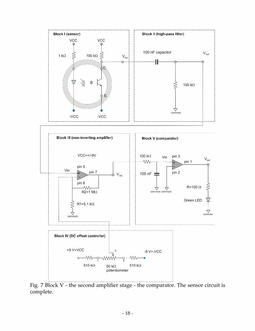
- 18 -
Fig. 7 Block V - the second amplifier stage - the comparator. The sensor circuit is complete.
- 19 -
NOTE: General way of tuning the circuit without the oscilloscope (if necessary): 1. Put the finger in the PVC tube and hold it in the same position; 2. Using the potentiometer, adjust to the maximum reading when the LED is
on during the largest period of time; 3. By slowly rotating the potentiometer knob in the opposite direction
achieve the state when the LED blinks synchronously with the heart rate.
Part III Questions
1. Why the sensor output voltage in Fig. 3 is high when the finger is in the
sensor and why is it low otherwise?
2. Why do we need the high-pass filter in the heart-rate sensor circuit from Fig. 7. Do you think the circuit without the filter will still function? Hint: short out the filter and observe the circuit operation.
3. What is the gain of the first amplifier stage (Block III) in Fig. 7?
4. What is the gain of the second amplifier stage (Block V) in Fig. 7?
5. The input voltage to the comparator amplifier is a sinusoidal function with
the amplitude of 1V. The amplifier rails are at ±10V. Assuming the ideal amplifier please plot the input and output voltages to scale over one period.
6. All electronic parts for the present laboratory cost about $6.50 total. A very similar in operation heart rate sensor from Pasco Scientific (http://www.pasco.com/) costs $80.00. It is listed in Appendix B. What do you think we are paying for?
7. Could you think of some possible applications of the present sensor concept?
8. This question is worth only one point of the laboratory grade. Please do not attempt this question if your time is limited. With the help of the present circuit and the built-in LabView signal processing tools, could you please try to precisely measure the heart rate for you and your partner? Consider the time duration of 30 sec as the base sampling window.
GT/SJB /SNM 09