Embed Size (px)
Citation preview

UNIVERSITI PUTRA MALAYSIA
DIGITAL SIGNAL PROCESSOR (DSP) DESIGN USING VERY LONG INSTRUCTION WORD (VLIW) ARCHITECTURE
LEE LINI @ LINI LEE
FK 2001 42

DIGITAL SIGNAL PROCESSOR (DSP) DESIGN USING VERY LONG INSTRUCTION WORD (VLIW) ARCIDTECTURE
By
LEE LINI @ LINI LEE
Thesis submitted in Fulfilment of the Requirement for the Degree of Master of Science in the Faculty of Engineering
Universiti Putra Malaysia
March 2001

Abstract of thesis presented to the Senate of Universiti Putra Malaysia in fulfilment of the requirement for the degree of Master of Science.
DIGITAL SIGNAL PROCESSOR (DSP) DESIGN USING VERY LONG INSTRUCTION WORD (VLIW) ARCHITECTURE
By
LEE LINI @ LINI LEE
March 2001
Chairman : Dr Bambang Sunaryo Suparjo
Faculty : Engineering
Programmable digital signal processors (PDSP) are microprocessors that
are specialized to perfonn well in digital signal processing-intensive
applications. A standard microprocessor can do most pDSP operations.
However, the pDSP chip has better ability to perfonn number crunching
algorithms simultaneously.
The objective of this research is to design and implement a general-
purpose programmable DSP (Digital Signal Processor) core. The architecture
of the pDSP core must be designed in such a way that parallel processing can be
carried out and computational units can be integrated into the core with ease. In
order to gain most benefit from the architecture, "Field Programmable Gate
Array" (FPGA) technology can be used. FPGA technology is a technology,
which gives the designer high flexibility in pDSP design. In order to fulfill the
requirement of pDSP, "Very Long Instruction Word" (VLIW) architecture
concept is used. Using, VHDL (Very-High-Speed-Integrated-Circuit Hardware
ii

Description Language) as design tool has the advantage in optimizing the pDSP
hardware requirement with ease where varying the size of units such as register
files (RF), program sequencer (PS), data address generator (DAG), arithmetic
logic unit (ALU), multiply-accumulator (MAC) and shifter can be done by
changing the data width or bit values. This flexibility of changing the data
width or bit values is suitable in VLIW architecture approach.
Based on the functional verification, the designed pDSP is able to
perform mathematical operations required in signal processing. The speed of
the operation is dependent on the size of the datapath as well as the type of
FPGA chips. It has been shown that changing the data width or bit values in the
VHDL source code of the subsystem can easily change the subsystems' sizes.
Thus, the time for redesign is significandy shorten.
Based on the verification done on Programmable Logic Device (PLO) of
MAX 7000s family, the operation can be executed in 40 MIPS (Million
instructions per second). However, higher MIPS value can be achieved by
using higher performance FPGAIPLO chip. Therefore, it is shown that VUW
architecture concept is suitable for microprocessor architecture and the pDSP
core is proven to be flexible in terms of size variation of the subsystems
consequently the variation of the operation speed.
iii

Abstrak tesis yang dikemukakan kepada Senat Universiti Putra Malaysia sebagai memenuhi keperluan untuk ijazah Master Sains
REKACIPT A PEMPROSES ISY ARA T DIGIT (DSP) MENGGUNAKAN SENIBINA VLIW
Oleh
LEE LINI @ LINI LEE
Mac 2001
Pengerusi : Dr Bambang Sunaryo Suparjo
Fakulti : Kejuruteraan
Pemproses isyarat digit bolehprogram merupakan pemprosesmikro yang
khusus dibina bagi memproses isyarat digit secara intensif. Pada lazimnya,
suatu pemprosesmikro biasa boleh melakukan kebanyakan operasi pemproses
isyarat digit bolehprogram. Walau bagaimanapun. pemproses isyarat digit
mempunyai Ic.eupayaan yang lebih baik untuk menjalankan banyak algoritma
secara serentak.
Objelc.tif penyelidikan ini adalah untuk merelc.abentuk satu pemproses
isyarat digit bolehprogram (pDSP) yang umum. Senibina pDSP ini perlu
direkabentuk agar pemprosesan secara selari boleh dijalankan dan unit
pengiraan boleh digabunglc.an ke dalam "core" dengan mudahnya. Pen&,ounaan
telc.nologi "Field Programmable Gate Array" (FPGA) boleh memaksimakan
Icelebihan yang terdapat dalam senibina pDSP. Telc.nologi FPGA merupakan
telc.nologi yang memberi pereka kebolehan mudahubah atau "flexibility" dalam
senibina pDSP. Bagi memenuhi keperluan pDSP tersebut. konsep senibina
iv

"Very Long Instruction Word" (VLIW) digunakan. Dengan menggunakan
"Very-High-Speed-Integrated-Circuit Hardware Description Language"
(VHDL) sebagai alat rekabentuk, ia mempunyai kelebihan untuk
memaksimakan keperluan perkakasan suatu pDSP dengan mUdahnya di mana
dengan mengubah saiz unit-unit seperti fail pendaftar (RF), penurut program
(PS), penjana alamat data (DAG), unit aritmetik logik (ALU), pendarab
pengumpul (MAC) dan pepindah, dan ini boleh dilakukan dengan mengubah
lebar data atau bilangan bit. Kelebihan untuk mengubah lebar data atau
bilangan bit ini adalah sesuai menggunakan pendekatan senibina VLIW.
Berpandukan pengesahan kefungsian sistem tersebut yang telah
dijalankan. pDSP yang telah direlcabentulc berlcebolehan untulc melakulcan
operasi Matematik seperti terdapat dalam pemprosesan isyarat. Kelajuan
operasi ini bergantung pada saiz "datapath" dan juga jenis cip FPGA yang
digunakan. Ia juga menunjukkan bahawa dengan mengubah lebar data atau
bilangan bit dalam kod-kod VHDL bagi subsistem pDSP, ianya mampu
menukar saiz subsistem tersebut dengan mUdahnya. Justeru itu, masa yang
diperlukan untuk merekabentuk semula suatu pDSP boleh dipendekkan.
Dengan menggunakan "Programmable Logic Device" (PLD) daripada
keluarga MAX 7000s sebagai pengesahan kefungsian, satu operasi boleh
terlaksana dalam 40 MIPS (Million instruction per second). Walau
bagaimanapun. bilangan MIPS yang lebih tinggi boleh dicapai dengan
menggunakan cip FPGAlPLD yang lebih berkemampuan untuk menghasilkan
v

prestasi yang lebih baik. Dengan itu, jelas ditunjukkan bahawa konsep senibina
VLIW adalah sesuai bagi senibina pemprosesmikro dan pDSP "core" ini dan
terbukti mempunyai sifat mudah diubahsuai dari segi perubahan saiz bagi
subsistem mahupun perubahan bagi keJajuan operas ian.
vi

ACKNOWLEDGEMENTS
First and foremost. I would like to express my utmost gratitude to my
project supervisor. Dr Bambang Sunaryo Suparjo, En Rahman Wagiran and Dr
Roslina Sidek for their invaluable guidance. constructive suggestion and
encouragement throughout the duration of the project.
My sincere gratitude goes to my group of friends who have directly and
indirectly help me to get through these years of study. W. B. Puah. P.B.Y. Tan.
G. H. Tan and C. L. Lee. thanks for lending your hands all this while. Not
forgetting my supportive group of friends (11). staff and consultants of the
Engineering Faculty. and people who have help made my years in University
more interesting and meaningful.
Words cannot express my deepest appreciation to my family especially
my parents and a very special friend of mine (P. L. Leong) for their undying
love. patience and support which have enable me to complete the project
successfully. Thank you very much for believing in me!
vii

I certify that an Examination Committee have met on 28th March 200 1 to conduct the final examination of Lee Lini @ Lini Lee on her Master of Science thesis entitled "Digital Signal Processor (DSP) Design using Very Long Instruction Word (VLIW) Architecture" in accordance with Universiti Pertanian Malaysia (Higher Degree) Act 1980 and Universiti Pertanian Malaysia (Higher Degree) Regulations 1981. The Committee recommends that the candidate be awarded the relevant degree. Members of the Examination Committee are as follows:
Norman Mariun. Ph.D. PEngo Associate Professor Faculty of Engineering. Universiti Putra Malaysia. (Chairman)
Bambang Sunaryo Suparjo. Ph.D. Faculty of Engineering. Universiti Putra Malaysia. (Member)
Rahman Wagiran. MSc. Faculty of Engineering. Universiti Putra Malaysia. (Member)
Roslina Sidek, Ph.D. Faculty of Engineering. Universiti Putra M:llaysia. (Member)
G� MOHA YIDIN. Ph.D. sor/Deputy Dean of Graduate School.
Universiti Putra Malaysia.
Date: 1 4 WAY 2DIJ1(
viii

This thesis submitted to the Senate of Universiti Putra Malaysia has been accepted as fulfilment of the requirement for the degree of Master of Science.
Date: 1 4 JUN 2001
ix

DECLARATION
I hereby declare that the thesis is based on my original work except for quotations and citations. which have been duly acknowledged. I declare that this thesis has not been previously or concurrentJy submitted for any other degree at UPM or other institutions.
(tEE J.i:� LEm
Date: Id·ry. dOD I
x

TABLE OF CONTENTS
ABSTRACT ABSTRAK ACKNOWLEDGEMENTS APPROV AL SHEETS DECLARATION FORM LIST OF TABLES LIST OF FIGURES LIST OF ABBREVIATIONS
CHAPTER
Page
ii iv vii viii x xiii XIV xv
1 INTRODUcrION ................................................................ .... 1 Digital Signal Processor ........................ ......... ................................................. 2
Programmable Digital Signal Processor (pDSP) and Field Programmable Gate A1:ray (FPGA) ................................................. .......... ..................... ......... 3
Objectives ........................................................................................................ 6
2 LITERATURE REVIEW .•••.....•........•.•••...•....•...••...•.•...•.•.......•. 8 Von Neumann Architecture ....... ......................................... ..................... ...... 10
Harvard architecture . ......................... ......... ....... ............ ...... ............ ............... 1 2
VLSI Computer Architecture for DSP .................................. ..... ................... 1 4
General Purpose Digital Signal Processor: Design Issues ..... ........................ 16
Very Long Instruction Word (VLlW) Architecture ......................... ............. 20
On--chip Memory .................. ......................................................................... 23
Summary ........................................................................................................ 24
3 DESIGN OF THE PDSP CORE .•.••.••. ••..•••...•••.•....•.•..•..•••.•.•...•• 25 Very High Speed Integrated Circuit (VHSIC) Hardware Description Language (VHDL) . ............................... . ........................................... ............. 27
Instruction Set Architecture ..................................... ......... ......... .................... 29
Methodology ......................................... ........... . ................................... ....... ... 33
Computational Units . .......... ............................................. .............................. 35 Arithmetic Logic Unit (ALU) ................................................................ 36 Multiplier Accumulator (MAC) .................................... ........................ 41
Shifter (with divider) module ....... ....................... .................................. 43
Data Address Generator (DAG) .............. ........... ........... ................................ 46
Register File ...................................... ................ .......... . ......... .. ............... ........ 51 Program Sequencer (PS) . ................. ................... .. . .... .......... . ............. . .......... . 52
The Fetch Unit ....................... ............................. ................................... 53
The Dispatch Units ............................... ................................................. 54
The Program Control Unit ...................................................... ..... .......... 55
xi

4 RESULTS AND DISCUSSION .•.•..•.......•....•..................••..•.•..• ..57 Arithmetic Logic Unit (ALU) ........................................................................ 57 8-bit Multiplier .............................................................................................. 62 8-bit Shifter .................................................................................................... 62 Data Address Generator (DAG) module ....................................................... 63 Register File ................................................................................................... 65 Instruction set architecture ............................................................................. 67 Example 1 ...................................................................................................... 71 Example 2 ...................................................................................................... 72 Discussion ...................................................................................................... 94
5 CONCLUSION AND FUTURE DEVELOPMENT .••••••••....•.••••.•.••. 96 Conclusion ..................................................................................................... 96 Future Development ...................................................................................... 98
REFERENCES .............. .................... . . . ................................ _ .. 100
APPENDICES
A B
c
VHDL source cooes ....................................... . . ....... 102 A divider module in Maxplus II environment . ....... " .... " ....... ""." .... " ....... " ................ " ........... 1 16 A datapatb module in Maxplus II environment." .................................. ...................................... " .............. " ..................... 1 17
D pDSP core including datapath A, datapatb B, shifter (with divider) module, DAG module and register files •.•.••..•..•• 1 18
E Datapath A and B (VLIW architecture) .•••••.•...•.•....•...•• 1 19
BIODATA OF THE AUTHOR •••.•..•.•..•••.••.••••....•••.••......•.••••.••.••• 120
xii
LIST OF TABLES
Page Table 3.1: ALU instructions . ........................................................................... 39
Table 4. 1 : Instruction cycles involved in Example 1 . ... ...................... ............ 7 1
Table 4. 2: Instruction cycles involved in Example 2 ...................................... 72
Table 4. 3: Organization of the timing diagram in Figure 4.3 . . ........................ 75
xiii
LIST OF FIGURES
Page Figure 1.1 Gate Array design flow . ................................................................... 5
Figure 2. 1: The "von Neumann" architecture . ....... .......................................... 11
Figure 2. 2: The Harvard architecture ................................................................ 12
Figure 2. 3: Parallel instruction and data stream ................................................ 1 3
Figure 2. 4: Space-time diagram for pipeline . ................................................... 17
Figure 2. 5: VLIW instruction word . ................................................................. 21
Figure 3. 1 : The core architecture of a DSP ....................................................... 25
Figure 3. 2: A single instruction set .................................................................. 31
Figure 3. 3: A general instruction format.. .... ................................. .................... 32
Figure 3. 4: The structure of ALU . ............................... ..................................... 36
Figure 3. 5: The ALU instruction format. .......................................................... 40 Figure 3. 6: Datapath with MAC module and separate ALU . .......................... . 41 Figure 3. 7: Datapath module ............................................................................. 42
Figure 3. 8: The instruction format of a shifter operation ....................... ........... 44 Figure 3. 9: A divider module . ........................................................................... 45
Figure 3. 1 0: General scheme of data address generator . ............................... . 47
Figure 3. 1 1 : The different DAG instructions .... . ............................................. 50
Figure 3. 1 2: Structure of a register file . .......................................................... 51 Figure 3. 1 3: Overviev. of a Program Sequencer ............................................. 53
Figure 3. 14: The instruction fetch unit. .......................................................... 54
Figure 3. 15: Overview of the dispatch units . .................................................. 55
Figure 4. 1: VLIW architecture with datapath A and B ..................................... 70
Figure 4. 2: Division algorithm . ......................................................................... 74
Figure 4.3: Output wavefonn simulation from the datapath . ............................ 76
xiv

LIST OF ABBREVIATIONS
AC -Carry out
AMOp -Specifies the ALU @ MAC operation
ALU -Arithmetic Logic Unit
AV -Overflow
AZ -Zero
CAD -Computer Aided Design
CI -Carry-in
COND -Condition
DAG -Data Address Generator
DMA -Data memory address
DMD -Data memory data
DSP -Digital Signal Processor
EX -Execute
FPGA -Field Programmable Gate Array
Funct -Variant of operation
HDL -Hardware Description Language
I/O -Input I Output
ID -Instruction Decode
ID field -Identifier field
IF -Instruction Fetch
L -Length
M -Modification
x.v

MAC -Multiply-Accumulator
MF -Multiplier feedback
MR -Multiplier result
Mux -Multiplexer
OF -Operands Fetch
Op -Operation code
PC -Program counter
pDSP -programmable Digital Signal Processor
PLD -Programmable Logic Device
PMA -Program memory address
PMD -Program memory data
PS -Program Sequencer
PSC unit -Program Sequencer Control unit
R -Result
Rd -Destination operand
RF -Register File
Rs -First SO{1rc� operands
Rt -Second S9urce operands
RT-DSP -Real Time Digital Signal Processing
Shamt -Shift amount
VHDL -Very-High-Sp--...ed-Integrated-Circuit Hardware Description Language
VHSIC -Very High Speed Integrated Circuit
VUW -Very Long Instruction Word
VLSI -Very Large Scale Integration
xvi

WR -Write
Xop -X operand
Y op -Y operand
Z -Destination register
xvii

CHAPTER 1
INTRODUCTION
With the introduction of new VLSI (Very Large Scale Integration)
techniques, it is now possible to implement entire systems in a single chip.
These new techniques and levels of integration allow the implementation of
specialized processors, which optimizes towards specific application. During
mid 1970's, Real-time Digital Signal Processing (RT-DSP) was an area whose
requirements were not achievable. Obviously, the requirements for real-time
digital signal processing are dependent of the application, but nomtally are large
enough for state of the art general-purpose microprocessors. One of the
proposed solutions, was the use of array processors, which achieved high
perfomtance levels through parallelism of most Digital Signal Processing
algorithm [Alers N. R. M., 1997].
In the early 19805, the first commercially successful DSP processors
were introduced. With that, there had been dozens of new processors
developed, offering system designers a vast array of choices. Today, DSPs are
widely used in multimedia applications, modems, cellular phones and disk-drive
controllers.
1

Digital Signal Processor
Basically, a digital signal processor is a microprocessor that has been
highly optimized for digital signal processing applications. A standard
microprocessor can do most DSP operations. However, the DSP chip has better
ability to perfonn number of algorithms in real time. In order to provide real
time processing, most DSPs have the ability to perfonn a multiply-and
accumulate (MAC) operation in a single instruction cycle. This MAC
operation, probably the most often cited feature of a DSP is highly useful in
many digital signal-processing applications such as digital filters, correlation
and Fourier Transfonns [Jensen T. 0., Holm 1. S. and Baltzersen F., 1998].
For signal processing tasks with moderate demands on the throughput, a
flexible hardware is desired that makes sequential processing of the subtasks
possible. In tenns of flexibility, there are various categories: from a hardware
structure controlled by few parameter line that allows a limited number of
different functions to a configuration programmed in a higher language that can
implement all algorithms practically.
Few of the fundamentals of DSPs have changed since the development
of the first DSP. The design of a nsp is affected by four factors: available
technology, targeted DSP algorithms, architectural optimizations, and
programming support. There is no doubt that technology is the driven force
behind the improvements to digital signal processor [Alers N. R. M., 1997].
2

Therefore a more flexible DSP should be introduced to overcome the limitations
faced by the present DSP chips.
The DSP core consists of three main parameterized functional units:
program control unit (PCU), datapath and data address generator. All the three
main units are able to access data memories through dedicated buses. The
datapath that accommodate a MAC unit, a shifter and an ALU are able to
execute all the core's data processing operations. Data address generator or
DAG provides data addresses and postmodifies the index registers if necessary.
The Program Control Unit or PCU, which consists of the execution control and
the instruction address generator controls operation of all core units and
additional off-core functional units. It usually obtains the program memory
address from either the program counter or the immediate address [Kuulusa M.,
Nunni J., Takala 1., Ojala P. and Herranen H., 1997].
Programmaole D;gital Signal Processor (PDSP) and Field Programmable Gate Array (FPGA)
Programmable Digital Signal Processors (PDSPs) are microprocessors
that are specialized to perform well in digital signal processing-intensive
applications. pDSPs are highly flexible because it can be reprogrammed.
Typically a pDSP contains several functional units to process the signal stream.
A designer encodes the algorithm into a program, which is executed by the
pDSP and is limited to a theoretical maximum data rate based on the speed and
the number of mUltipliers or accumulators in the device. Applications that
3

require several computations must be broken up into a sequential stream of
computations.
Programmable DSP chips are intrinsically limited in perfonnance. The
more data sample to be processed, the more cycles are needed and the slower
data is processed. One way to overcome this limitation is to use the Field
Programmable Gate Arrays (FPGA) technology, a technology which gives
designer a combination benefit of both gate array solution and the ease of pDSP
design [Xilinx Inc., 1997].
A FPGA design starts with a circuit schematic or high-level design
description. Gate Array technology offers the ability to do many things in
parallel. A Gate Array is a custom chip that allows very specific
implementations of digital circuits to be constructed. It is an open grid of sites,
which can be occupied by logic cells selected from a library. A schematic
diagram can be drawn and then automatic tools of the FPGA technology will
place the components of the circuit into the Gate Array sites.
Advantages of FPGAs include that parts of the design may be
reprogrammed over and if there is a need to upgrade the design, what it needed
is only reprogramming. FPGAs are pre-tested, which means that the traditional
Gate Array design methodology requires costly manufacturing test suites unlike
FPGAs. FPGAs are commodity part and therefore, production volume results
in a lower per part cost. FPGAs can be dynamically reconfigured within the
4

system. Systems can be built adapting to changing conditions by altering the
circuit configured within the FPGA. This re-configurable approach is popular
since many systems need to perfonn several different functions [Xilinx Inc.,
1997] ..
Schematic or .. Translation ... Gate array HDL
r- r description
" Gate
Fabrication ... array r'
chip
Figure 1. 1 Gate Array design flow.
An alternative to using a schematic for the design description is to use a
Hardware Description Language (HDL). HDL is a high level description of
circuit behavior. These higher level descriptions are easier to create and
understand than schematics and it looks like programming language. Very High
Speed Integrated Circuit (VHSIC) HDL or VHDL as it is commonly known
supports the design, documentation and efficient simulation of hardware from
the digital system level to the gate level. It is used to model digital hardware
and the synthesized code can be used as input to hardware synthesis tool.
5
With the limitations faced by the present DSP chips, programmable DSP
chips are introduced. However, there are still performance limitations in the
pDSPs. Therefore, with the combination of both FPGA technology and the
VHDL synthesized codes, one flexible pDSP can be designed which will
compromise all the factors that affect the improvement of a DSP.
Objectives
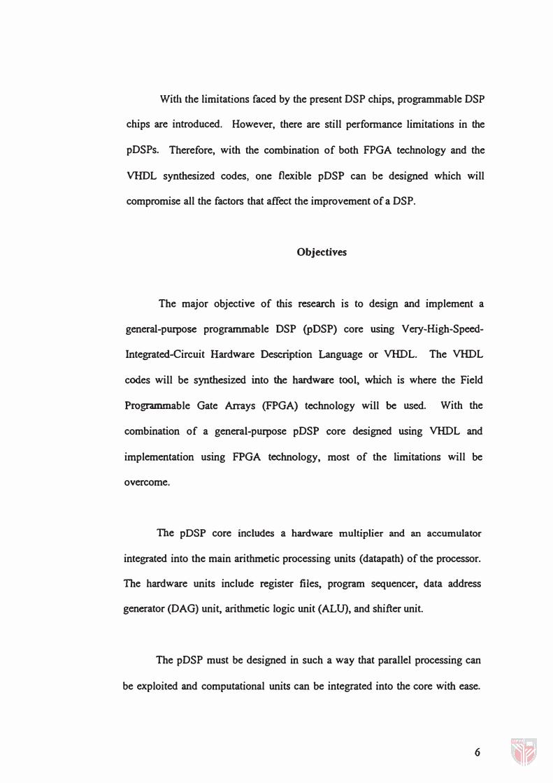
The major objective of this research is to design and implement a
general-purpose programmable DSP (PDSP) core using Very-High-Speed
Integrated-Circuit Hardware Description Language or VHDL. The VHDL
codes will be synthesized into the hardware tool, which is where the Field
Programmable Gate Arrays (FPGA) technology will be used. With the
combination of a general-purpose pDSP core designed using VHDL and
implementation using FPGA technology, most of the limitations will be
overcome.
The pDSP core includes a hardware multiplier and an accumulator
integrated into the main arithmetic processing units (datapath) of the processor.
The hardware units include register files, program sequencer, data address
generator (DAG) unit, arithmetic logic unit (ALU), and shifter unit.
The pDSP must be designed in such a way that parallel processing can
be exploited and computational units can be integrated into the core with ease.
6

The idea of this work is to utilize the concept of Very Long Instruction Word
(VLIW) architecture into the pDSP architecture. The attraction of the VLIW
architecture is the ability to execute multiple instructions per cycle.
7