Embed Size (px)
Citation preview
MSP430 Family USART Peripheral Interface
12-I
12
13
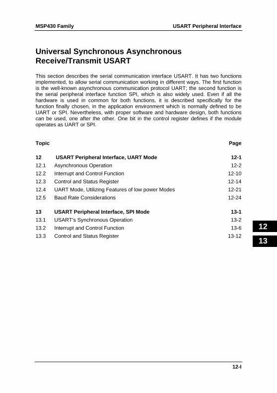
Universal Synchronous AsynchronousReceive/Transmit USART
This section describes the serial communication interface USART. It has two functionsimplemented, to allow serial communication working in different ways. The first functionis the well-known asynchronous communication protocol UART; the second function isthe serial peripheral interface function SPI, which is also widely used. Even if all thehardware is used in common for both functions, it is described specifically for thefunction finally chosen, in the application environment which is normally defined to beUART or SPI. Nevertheless, with proper software and hardware design, both functionscan be used, one after the other. One bit in the control register defines if the moduleoperates as UART or SPI.
Topic Page
12 USART Peripheral Interface, UART Mode 12-1
12.1 Asynchronous Operation 12-2
12.2 Interrupt and Control Function 12-10
12.3 Control and Status Register 12-14
12.4 UART Mode, Utilizing Features of low power Modes 12-21
12.5 Baud Rate Considerations 12-24
13 USART Peripheral Interface, SPI Mode 13-1
13.1 USART’s Synchronous Operation 13-2
13.2 Interrupt and Control Function 13-6
13.3 Control and Status Register 13-12
USART Peripheral Interface MSP430 Family
12-II
12
13
MSP430 Family USART Peripheral Interface
12-III
12
13
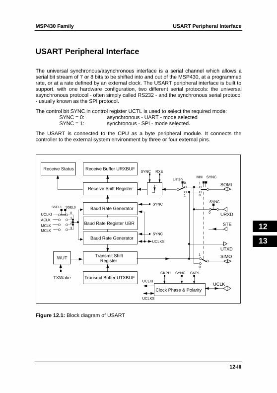
USART Peripheral Interface
The universal synchronous/asynchronous interface is a serial channel which allows aserial bit stream of 7 or 8 bits to be shifted into and out of the MSP430, at a programmedrate, or at a rate defined by an external clock. The USART peripheral interface is built tosupport, with one hardware configuration, two different serial protocols: the universalasynchronous protocol - often simply called RS232 - and the synchronous serial protocol- usually known as the SPI protocol.
The control bit SYNC in control register UCTL is used to select the required mode:SYNC = 0: asynchronous - UART - mode selectedSYNC = 1: synchronous - SPI - mode selected.
The USART is connected to the CPU as a byte peripheral module. It connects thecontroller to the external system environment by three or four external pins.
Receive Buffer URXBUF
Receive Shift Register
Baud Rate Generator
Transmit ShiftRegister
Transmit Buffer UTXBUF
Receive Status
WUT
TXWake
RXE
CKPL
UCLKI
MCLK
ACLK
SSEL1 SSEL0
0
12
3MCLK
Baud Rate Generator
Baud Rate Register UBR
SYNC
Listen0 1 SOMI
1 0
1 SIMO
0
MM
UCLKClock Phase & Polarity
CKPH
UCLKI
UCLKS
SYNC
UCLKS
SYNC
SYNC
URXD
UTXD
SYNC
0
SYNC
STE
Figure 12.1: Block diagram of USART

USART Peripheral Interface MSP430 Family
12-IV
12
13
MSP430 Family USART Peripheral Interface, UART Mode
12-1
12
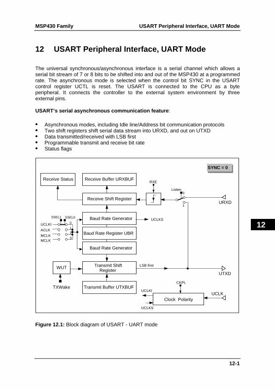
12 USART Peripheral Interface, UART Mode
The universal synchronous/asynchronous interface is a serial channel which allows aserial bit stream of 7 or 8 bits to be shifted into and out of the MSP430 at a programmedrate. The asynchronous mode is selected when the control bit SYNC in the USARTcontrol register UCTL is reset. The USART is connected to the CPU as a byteperipheral. It connects the controller to the external system environment by threeexternal pins.
USART’s serial asynchronous communication feature :
•• Asynchronous modes, including Idle line/Address bit communication protocols•• Two shift registers shift serial data stream into URXD, and out on UTXD•• Data transmitted/received with LSB first•• Programmable transmit and receive bit rate•• Status flags
Receive Buffer URXBUF
Receive Shift Register
Baud Rate Generator
Transmit ShiftRegister
Transmit Buffer UTXBUF
Receive Status
WUT
TXWake
RXE
CKPL
UCLKI
MCLK
ACLK
SSEL1 SSEL0
0
12
3MCLK
Baud Rate Generator
Baud Rate Register UBR
Listen0
1
UCLKClock Polarity
UCLKI
UCLKS
UCLKS
URXD
UTXD
LSB first
SYNC = 0
Figure 12.1: Block diagram of USART - UART mode
USART Peripheral Interface, UART Mode MSP430 Family
12-2
12
12.1 Asynchronous Operation
In the asynchronous mode, the receiver synchronizes itself to frames, but the externaltransmitting and receiving devices do not use the same clock source; the baud rate isgenerated locally.
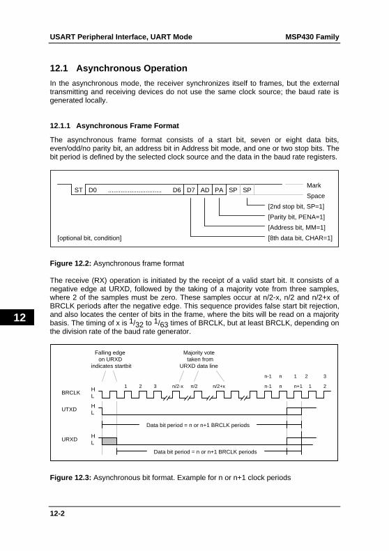
12.1.1 Asynchronous Frame Format
The asynchronous frame format consists of a start bit, seven or eight data bits,even/odd/no parity bit, an address bit in Address bit mode, and one or two stop bits. Thebit period is defined by the selected clock source and the data in the baud rate registers.
[Address bit, MM=1]
[Parity bit, PENA=1]
D0
[8th data bit, CHAR=1]
ST D7D6..............................
[2nd stop bit, SP=1]
Mark
SpacePA SP SP
[optional bit, condition]
AD
Figure 12.2: Asynchronous frame format
The receive (RX) operation is initiated by the receipt of a valid start bit. It consists of anegative edge at URXD, followed by the taking of a majority vote from three samples,where 2 of the samples must be zero. These samples occur at n/2-x, n/2 and n/2+x ofBRCLK periods after the negative edge. This sequence provides false start bit rejection,and also locates the center of bits in the frame, where the bits will be read on a majoritybasis. The timing of x is 1/32 to 1/63 times of BRCLK, but at least BRCLK, depending onthe division rate of the baud rate generator.
1 2 3
Falling edgeon URXD
indicates startbit
Majority votetaken from
URXD data line
1 2
Data bit period = n or n+1 BRCLK periods
BRCLKHL
UTXDHL
Data bit period = n or n+1 BRCLK periods
URXDHL
n/2n/2-x n/2+x n n+1
1 2n-1 n 3
n-1
Figure 12.3: Asynchronous bit format. Example for n or n+1 clock periods
MSP430 Family USART Peripheral Interface, UART Mode
12-3
12
12.1.2 Baud rate generation in asynchronous communication format
The baud rate generation in the MSP430 differs from other standard serialcommunication interface implementations.
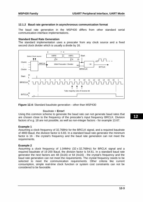
Standard Baud Rate GenerationThe standard implementation uses a prescaler from any clock source and a fixedsecond clock divider which is usually a divide by 16.
16bit Prescaler / Divider
15
UBR0 UBR1
0 7 0 7
8 8
Clock1
Select Clock source
BRSCLKHL
StartHL
BRCLK
BITCLK
BITCLKHL
Start
:Clockn
: RC : 16
1 2 3 4 5 6 7 8 9 10 11 12 13 14 15 16 1
Take majority vote of receive bit
BRSCLK
Figure 12.4: Standard baudrate generation - other than MSP430
Baudrate = Error!Using this common scheme to generate the baud rate can not generate baud rates thatare chosen close to the frequency of the prescaler’s input frequency BRCLK. Divisionfactors of e.g. 18 are not possible, as well as non-integer factors - for example 13.67.
Example 1Assuming a clock frequency of 32,768Hz for the BRCLK signal, and a required baudrateof 4800 Baud, the division factor is 6.83. In a standard baud rate generator the minimumfactor is 16 - the crystal’s frequency and the baud rate generation can not meet therequirements.
Example 2Assuming a clock frequency of 1.04MHz (32 x 32,768Hz) for BRCLK signal and arequired baudrate of 19 200 Baud, the division factor is 54.61. In a standard baud rategenerator the next factors are 48 (3x16) or 64 (4x16) - the crystal’s frequency and thebaud rate generation can not meet the requirements. The crystal frequency needs to beselected to meet the communication requirements. Other criteria like currentconsumption, simple real-time clock function or system cost constraints can not beconsidered to be favorable.
USART Peripheral Interface, UART Mode MSP430 Family
12-4
12
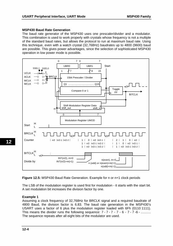
MSP430 Baud Rate GenerationThe baud rate generator of the MSP430 uses one prescaler/divider and a modulator.This combination is used to work properly with crystals whose frequency is not a multipleof the standard baud rates, but allows the protocol to run at maximum baud rate. Usingthis technique, even with a watch crystal (32,768Hz) baudrates up to 4800 (9600) baudare possible. This gives power advantages, since the selection of sophisticated MSP430operation in low power mode is possible.
1n/2 n/2-1
15bit Prescaler / Divider
151
UBR0 UBR1
0 7 0 7
Q1 ...................................... Q15
Compare 0 or 1
7 8
Shift Modulation Register Data
Modulation Register UMOD
UCLK
MCLK
ACLK
SSEL1 SSEL0
0
1
2
3MCLK
BRCLKHL
StartHL
Counter
BRCLK
BITCLK
BITCLKHL
0 7
m
Divide by
0n/2-2
n/2
n/2
n/2-1
12 0n/2
n/2
n/2-11 0n/2 n/2-1 n/2 n/2-1
11
n(even), m=0n (odd) or n(even)+m(=1)
n(odd)+m(=1)
Start
INT(n/2), m=0INT(n/2)+m(=1)
n/2-21
n/2-1
n/2-2
n/2-2
shift_inshift_out
ToggleFF
Figure 12.5: MSP430 Baud Rate Generation. Example for n or n+1 clock periods
The LSB of the modulation register is used first for modulation - it starts with the start bit.A set modulation bit increases the division factor by one.
Example 1Assuming a clock frequency of 32,768Hz for BRCLK signal and a required baudrate of4800 Baud, the division factor is 6.83. The baud rate generation in the MSP430’sUSART uses a factor of 6 plus the modulation register loaded with 6Fh (0110 1111).This means the divider runs the following sequence: 7 - 7 - 7 - 7 - 6 - 7 - 7 -6 - ...........The sequence repeats after all eight bits of the modulator are used.
MSP430 Family USART Peripheral Interface, UART Mode
12-5
12
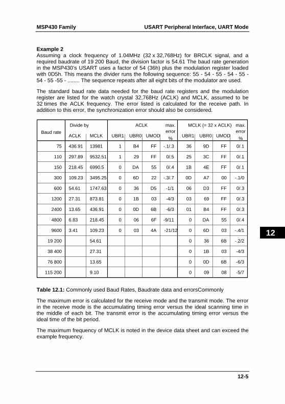
Example 2Assuming a clock frequency of 1.04MHz (32 x 32,768Hz) for BRCLK signal, and arequired baudrate of 19 200 Baud, the division factor is 54.61 The baud rate generationin the MSP430’s USART uses a factor of 54 (36h) plus the modulation register loadedwith 0D5h. This means the divider runs the following sequence: 55 - 54 - 55 - 54 - 55 -54 - 55 -55 - ........ The sequence repeats after all eight bits of the modulator are used.
The standard baud rate data needed for the baud rate registers and the modulationregister are listed for the watch crystal 32,768Hz (ACLK) and MCLK, assumed to be32 times the ACLK frequency. The error listed is calculated for the receive path. Inaddition to this error, the synchronization error should also be considered.
Baud rateUBR1
Divide by
UBR0 UMOD
75
110
150
300
600
1200
2400
4800
9600
19 200
38 400
76 800
115 200
ACLK MCLK
436.91
297.89
218.45
109.23
54.61
27.31
13.65
6.83
3.41
13981
9532.51
6990.5
3495.25
1747.63
873.81
436.91
218.45
109.23
54.61
27.31
13.65
9.10
ACLK
UBR1 UBR0 UMOD
MCLK (= 32 x ACLK)errormax.
errormax.
1 B4
1 29
0 DA
0 6D
0 36
0 1B
0 0D
0 06
0 03
01 B4
03 69
0 DA
0 6D
0 36
0 1B
0 09
36 9D
25 3C
1B 4E
0D A7
06 D3
0 0D
FF
FF
55
22
D5
03
6B
6F
4A
-9/11
-6/3
-4/3
-1/1
-.3/.7
0/.4
0/.5
-.1/.3
-21/12
FF
FF
55
03
6B
03
08
FF
FF
FF
00
FF
6B
0/.3
0/.3
0/.4
-.4/1
-.2/2
-4/3
-5/7
-6/3
0/.3
-.1/0
0/.1
0/.1
0/.1
%%
Table 12.1: Commonly used Baud Rates, Baudrate data and errorsCommonly
The maximum error is calculated for the receive mode and the transmit mode. The errorin the receive mode is the accumulating timing error versus the ideal scanning time inthe middle of each bit. The transmit error is the accumulating timing error versus theideal time of the bit period.
The maximum frequency of MCLK is noted in the device data sheet and can exceed theexample frequency.
USART Peripheral Interface, UART Mode MSP430 Family
12-6
12
12.1.3 Asynchronous Communication Formats
The USART module supports two multiprocessor communication modes when theasynchronous mode is used. These formats can be used to transfer informationbetween many microcomputers on the same serial link. Information is transferred as ablock of frames from a particular source to one or more destinations. The USART hasfeatures to identify the start of blocks, and to suppress interrupts and status informationfrom the receiver, until a block start is identified. In both multiprocessor modes, thesequence of data exchange with the USART module could be based on polling of data,or using the receive interrupt features.
Both asynchronous multiprocessor protocols, the idle line and the address bitmultiprocessor mode allow efficient data transfer between multiple communicationsystems. They also can be used to minimize activity of the system, whether to savecurrent consumption or processing resources. The MM bit in the control register definesthe address bit or idle line multiprocessor protocol mode. Both formats use the wake upon transmitting, using the address feature function (TXWake bit), and on activating theRXWake bit. The URXWIE and URXIE bits control the transmit and receive features ofthese modes.
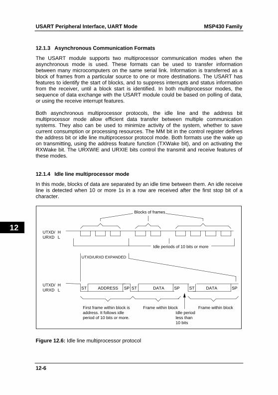
12.1.4 Idle line multiprocessor mode
In this mode, blocks of data are separated by an idle time between them. An idle receiveline is detected when 10 or more 1s in a row are received after the first stop bit of acharacter.
Blocks of frames
UTXD/ HURXD L
Idle periods of 10 bits or more
ST ADDRESS SP ST DATA SP ST DATA SP
UTXD/URXD EXPANDED
UTXD/ HURXD L
First frame within block isaddress. It follows idleperiod of 10 bits or more.
Frame within blockIdle periodless than10 bits
Frame within block
Figure 12.6: Idle line multiprocessor protocol
MSP430 Family USART Peripheral Interface, UART Mode
12-7
12
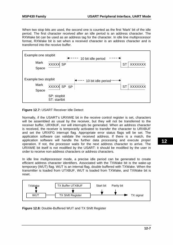
When two stop bits are used, the second one is counted as the first 'Mark' bit of the idleperiod. The first character received after an idle period is an address character. TheRXWake bit can be used as an address tag for the character. In idle line multiprocessorformat, RXWake bit is set when a received character is an address character and istransferred into the receive buffer.
Example:one stopbit
XXXXX SP
10 bit idle period
ST XXXXXXX
XXXXX SP ST XXXXXXXSP
Mark
Space
Mark
Space
SP: stopbitST: startbit
10 bit idle periodExample:two stopbit
Figure 12.7: USART Receiver Idle Detect
Normally, if the USART’s URXWIE bit in the receive control register is set, characterswill be assembled as usual by the receiver, but they will not be transferred to thereceiver buffer, URXBUF, nor will interrupts be generated. When an address characteris received, the receiver is temporarily activated to transfer the character to URXBUFand set the URXIFG interrupt flag. Appropriate error status flags will be set. Theapplication software can validate the received address. If there is a match, theapplication software will handle the further data processing and execute properoperation. If not, the processor waits for the next address character to arrive. TheURXWIE bit itself is not modified by the USART: it should be modified by the user inorder to receive non-address characters or address characters.
In idle line multiprocessor mode, a precise idle period can be generated to createefficient address character identifiers. Associated with the TXWake bit is the wake-uptemporary (WUT) flag. WUT is an internal flag, double buffered with TXWake. When thetransmitter is loaded from UTXBUF, WUT is loaded from TXWake, and TXWake bit isreset.
TXWake TX Buffer UTXBUF
TX signal
Start bit Parity bit
WUT TX Shift Register
Figure 12.8: Double-Buffered WUT and TX Shift Register
USART Peripheral Interface, UART Mode MSP430 Family
12-8
12
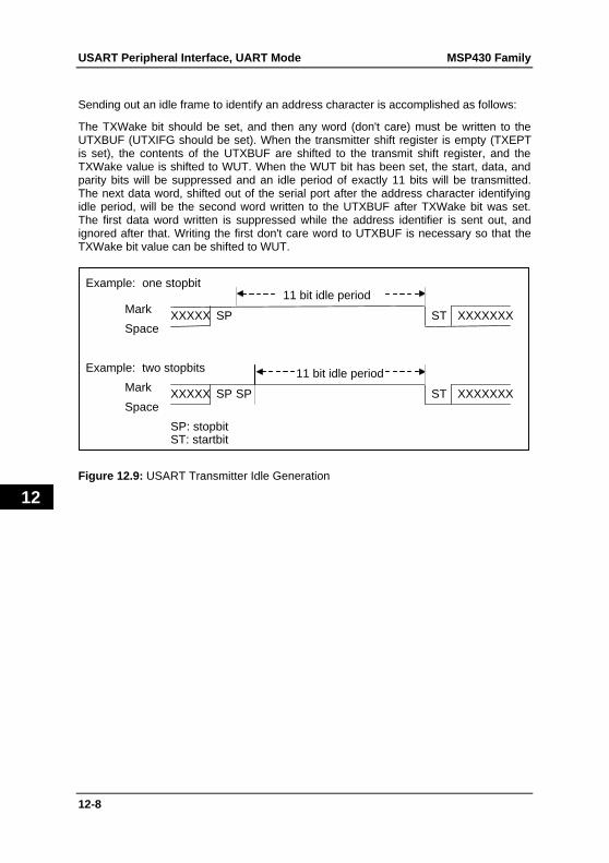
Sending out an idle frame to identify an address character is accomplished as follows:
The TXWake bit should be set, and then any word (don't care) must be written to theUTXBUF (UTXIFG should be set). When the transmitter shift register is empty (TXEPTis set), the contents of the UTXBUF are shifted to the transmit shift register, and theTXWake value is shifted to WUT. When the WUT bit has been set, the start, data, andparity bits will be suppressed and an idle period of exactly 11 bits will be transmitted.The next data word, shifted out of the serial port after the address character identifyingidle period, will be the second word written to the UTXBUF after TXWake bit was set.The first data word written is suppressed while the address identifier is sent out, andignored after that. Writing the first don't care word to UTXBUF is necessary so that theTXWake bit value can be shifted to WUT.
Example: one stopbit
XXXXX SP
11 bit idle period
ST XXXXXXX
XXXXX SP ST XXXXXXXSP
Mark
Space
Mark
Space
SP: stopbitST: startbit
11 bit idle periodExample: two stopbits
Figure 12.9: USART Transmitter Idle Generation
MSP430 Family USART Peripheral Interface, UART Mode
12-9
12
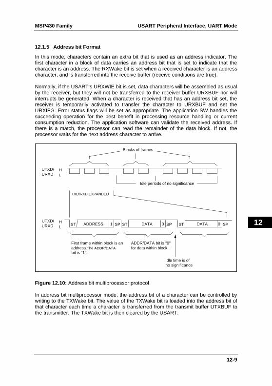
12.1.5 Address bit Format
In this mode, characters contain an extra bit that is used as an address indicator. Thefirst character in a block of data carries an address bit that is set to indicate that thecharacter is an address. The RXWake bit is set when a received character is an addresscharacter, and is transferred into the receive buffer (receive conditions are true).
Normally, if the USART’s URXWIE bit is set, data characters will be assembled as usualby the receiver, but they will not be transferred to the receiver buffer URXBUF nor willinterrupts be generated. When a character is received that has an address bit set, thereceiver is temporarily activated to transfer the character to URXBUF and set theURXIFG. Error status flags will be set as appropriate. The application SW handles thesucceeding operation for the best benefit in processing resource handling or currentconsumption reduction. The application software can validate the received address. Ifthere is a match, the processor can read the remainder of the data block. If not, theprocessor waits for the next address character to arrive.
Blocks of frames
UTXD/ HURXD L
Idle periods of no significance
ST ADDRESS SP ST DATA SP ST DATA SP
TXD/RXD EXPANDED
UTXD/ HURXD L
First frame within block is anaddress.The ADDR/DATAbit is "1".
ADDR/DATA bit is "0"for data within block.
Idle time is ofno significance
1 0 0
Figure 12.10: Address bit multiprocessor protocol
In address bit multiprocessor mode, the address bit of a character can be controlled bywriting to the TXWake bit. The value of the TXWake bit is loaded into the address bit ofthat character each time a character is transferred from the transmit buffer UTXBUF tothe transmitter. The TXWake bit is then cleared by the USART.
USART Peripheral Interface, UART Mode MSP430 Family
12-10
12
12.2 Interrupt and Control Function
The USART peripheral serves two main interrupt sources, for transmission andreception. Two individual interrupt vectors are available, one for receive and one fortransmit interrupt events.
The control bits of the USART are located in the SFR address range:
• Receive Interrupt Flag URXIFG initial state reset (by PUC/SWRST)• Receive Interrupt Enable URXIE initial state reset (by PUC/SWRST)• Receive Enable URXE initial state reset (by PUC)• Transmit Interrupt Flag UTXIFG initial state set (by PUC/SWRST)• Transmit Interrupt Enable UTXIE initial state reset (by PUC/SWRST)• Transmit Enable UTXE initial state reset (by PUC)
The receiver and transmitter of the USART operate fully independently, but use thesame baud rate generator. Transmit and receive use the same baud rate.
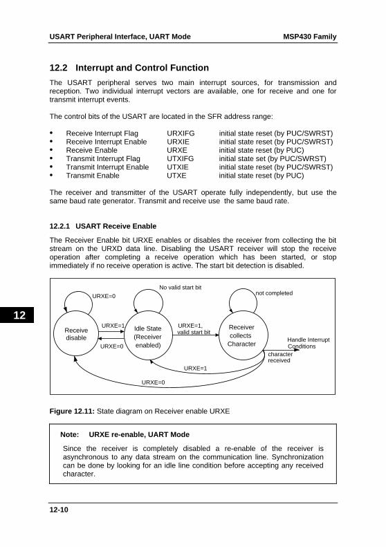
12.2.1 USART Receive Enable
The Receiver Enable bit URXE enables or disables the receiver from collecting the bitstream on the URXD data line. Disabling the USART receiver will stop the receiveoperation after completing a receive operation which has been started, or stopimmediately if no receive operation is active. The start bit detection is disabled.
Idle State(Receiverenabled)
Receivedisable
Receivercollects
Character
URXE=0
URXE=1
URXE=0
No valid start bit
valid start bit
URXE=0
not completed
Handle InterruptConditions
characterreceived
URXE=1,
URXE=1
Figure 12.11: State diagram on Receiver enable URXE
Note: URXE re-enable, UART Mode
Since the receiver is completely disabled a re-enable of the receiver isasynchronous to any data stream on the communication line. Synchronizationcan be done by looking for an idle line condition before accepting any receivedcharacter.
MSP430 Family USART Peripheral Interface, UART Mode
12-11
12
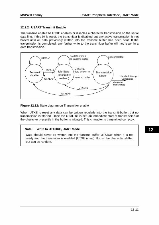
12.2.2 USART Transmit Enable
The transmit enable bit UTXE enables or disables a character transmission on the serialdata line. If this bit is reset, the transmitter is disabled but any active transmission is nothalted until all data previously written into the transmit buffer has been sent. If thetransmission is completed, any further write to the transmitter buffer will not result in adata transmission.
Idle State(Transmitter
enabled)
Transmitdisable
Transmissionactive
UTXE=0
UTXE=1
UTXE=0
no data writtento transmit buffer
data written to
UTXE=0
not completed
Handle InterruptConditions
charactertransmitted
UTXE=1,
UTXE=1
transmit buffer
Figure 12.12: State diagram on Transmitter enable
When UTXE is reset any data can be written regularly into the transmit buffer, but notransmission is started. Once the UTXE bit is set, an immediate start of transmission ofthe character presently in the buffer is initiated. This character is transmitted correctly.
Note: Write to UTXBUF, UART Mode
Data should never be written into the transmit buffer UTXBUF when it is notready and the transmitter is enabled (UTXE is set). If it is, the character shiftedout can be random.
USART Peripheral Interface, UART Mode MSP430 Family
12-12
12
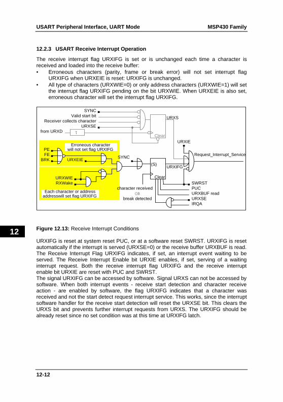
12.2.3 USART Receive Interrupt Operation
The receive interrupt flag URXIFG is set or is unchanged each time a character isreceived and loaded into the receive buffer:• Erroneous characters (parity, frame or break error) will not set interrupt flag
URXIFG when URXEIE is reset: URXIFG is unchanged.• All type of characters (URXWIE=0) or only address characters (URXWIE=1) will set
the interrupt flag URXIFG pending on the bit URXWIE. When URXEIE is also set,erroneous character will set the interrupt flag URXIFG.
URXIE
URXIFG
PUCSWRST
URXBUF read
IRQA
Clear
Request_Interrupt_Service
ORbreak detected
URXS
Clear
URXSEfrom URXD
Receiver collects characterValid start bit
τ
SYNC
PE
URXEIE
URXWIERXWake
FE
Erroneous characterwill not set flag URXIFG
character receivedEach character or address
addresswill set flag URXIFG
SYNC
URXSE
BRK(S)
Figure 12.13: Receive Interrupt Conditions
URXIFG is reset at system reset PUC, or at a software reset SWRST. URXIFG is resetautomatically if the interrupt is served (URXSE=0) or the receive buffer URXBUF is read.The Receive Interrupt Flag URXIFG indicates, if set, an interrupt event waiting to beserved. The Receive Interrupt Enable bit URXIE enables, if set, serving of a waitinginterrupt request. Both the receive interrupt flag URXIFG and the receive interruptenable bit URXIE are reset with PUC and SWRST.The signal URXIFG can be accessed by software. Signal URXS can not be accessed bysoftware. When both interrupt events - receive start detection and character receiveaction - are enabled by software, the flag URXIFG indicates that a character wasreceived and not the start detect request interrupt service. This works, since the interruptsoftware handler for the receive start detection will reset the URXSE bit. This clears theURXS bit and prevents further interrupt requests from URXS. The URXIFG should bealready reset since no set condition was at this time at URXIFG latch.
MSP430 Family USART Peripheral Interface, UART Mode
12-13
12
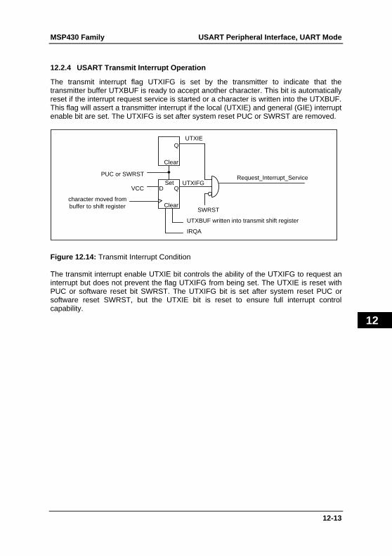
12.2.4 USART Transmit Interrupt Operation
The transmit interrupt flag UTXIFG is set by the transmitter to indicate that thetransmitter buffer UTXBUF is ready to accept another character. This bit is automaticallyreset if the interrupt request service is started or a character is written into the UTXBUF.This flag will assert a transmitter interrupt if the local (UTXIE) and general (GIE) interruptenable bit are set. The UTXIFG is set after system reset PUC or SWRST are removed.
UTXIE
UTXIFG
PUC or SWRST
UTXBUF written into transmit shift register
IRQA
character moved fromClear
Request_Interrupt_Service
buffer to shift register
VCCSet
D Q
Clear
Q
SWRST
Figure 12.14: Transmit Interrupt Condition
The transmit interrupt enable UTXIE bit controls the ability of the UTXIFG to request aninterrupt but does not prevent the flag UTXIFG from being set. The UTXIE is reset withPUC or software reset bit SWRST. The UTXIFG bit is set after system reset PUC orsoftware reset SWRST, but the UTXIE bit is reset to ensure full interrupt controlcapability.
USART Peripheral Interface, UART Mode MSP430 Family
12-14
12
12.3 Control and Status Register
The USART module hardware is byte structured and should be accessed by byteprocessing instructions (suffix 'B').
Register short form Register type Address Initial state
• USART Control register UCTL Type of read/write 070h See ....• Transmit Control register UTCTL Type of read/write 071h individual ...• Receive Control register URCTL Type of read/write 072h bit description• Modulation Control reg. UMCTL Type of read/write 073h unchanged• Baud Rate register 0 UBR0 Type of read/write 074h unchanged• Baud Rate register 1 UBR1 Type of read/write 075h unchanged• Receive Buffer URXBUF Type of read/write 076h unchanged• Transmit Buffer UTXBUF Type of read 077h unchanged
All bits are random after PUC, unless noted otherwise by the detailed functionaldescription.Reset of the USART is performed by PUC or SWRST bit. After power-up clear (PUC)the SWRST bit remains set and the USART remains in this condition until the reset isdisabled by resetting the SWRST bit.The USART module operates in asynchronous or in synchronous mode defined by theSYNC bit. The bits in the control registers may have different functions in the twomodes. All bits in this section are described with their functions in the asynchronousmode - SYNC=0. Their functions in the synchronous mode are described in theUSART’s serial peripheral interface section.
12.3.1 USART Control register UCTL
The information stored in the control register determines the basic operation of theUSART module. The register bits select the communications protocol, communicationmode and parity bit. All bits should be programmed according to the selected modebefore reset is disabled by resetting bit SWRST.
UCTL
rw-0 rw-0 rw-0 rw-0 rw-0 rw-0 rw-0 rw-1070h
7 0
SWRSTMMSYNCListenCHARSPPEVPENA
Figure 12.15: USART Control Register UCTL
Bit 0: The USART state machines and operating flags are initialized to the resetcondition if the software reset bit is set. Until the SWRST bit is reset, allaffected logic is held in the reset state. This implies that after a system resetthe USART must be re-enabled by resetting this bit. The receive andtransmit enable flags URXE and UTXE are not altered by SWRST.
MSP430 Family USART Peripheral Interface, UART Mode
12-15
12
Bit 1: Multiprocessor mode (address/idle line wake up).Two multiprocessor protocols, idle line and address bit, are supported by theUSART module. The choice of multiprocessor mode affects the operation ofthe automatic address decoding functions.MM = "0" : Idle line multiprocessor protocolMM = "1" : Address bit multiprocessor protocolThe conventional asynchronous protocol uses MM bit reset
Bit 2: Mode or function of USART module selected.The SYNC bit selects the function of the USART peripheral interfacemodule. Some of the USART control bits will have different functions inUART and SPI mode.SYNC = 0 : UART function is selected.SYNC = 1 : SPI function is selected.
Bit 3: The Listen bit selects if the transmitted data is fed back internally to thereceiver.Listen = 0 : No feed back.Listen = 1 : Transmit signal is internally fed back to the receiver. Each
transmission from the MSP430’s USART is received paralleland no external signal is received anymore.
Bit 4: Character length.This register bit selects the length of the character to be transmitted as 7 or8 bits. Characters of 7 bits do not use the eighth bit in URXBUF andUTXBUF and this bit is padded with "0".CHAR = 0 : 7 bit data.CHAR = 1 : 8 bit data.
Bit 5: Number of stop bits.This bit determines the number of stop bits transmitted. The receiver checksfor one stop bit only.SP = 0 : one stop bit.SP = 1 : two stop bits.
Bit 6: Parity odd/even.If PENA bit is set (parity bit is enabled), the PEV bit defines odd or evenparity according to the number of odd or even "1" bits in both transmittedand received characters, address bit (address bit multiprocessor mode) andparity bit.PEV = 0 : Odd parityPEV = 1 : Even parity.
Bit 7: Parity enable.If parity is disabled no parity bit is generated during transmission orexpected during reception. A received parity bit is not transferred to theURXBUF with the received data as it is not considered as one of the databits. During address bit multiprocessor mode, the address bit is included inthe parity calculation.PEN = 0 : Parity disablePEN = 1 : Parity enable
USART Peripheral Interface, UART Mode MSP430 Family
12-16
12
Note: MARK, SPACE definition
The MARK condition is identically to the signal level in the idle state. SPACE isthe opposite signal level: the start bit is always SPACE.
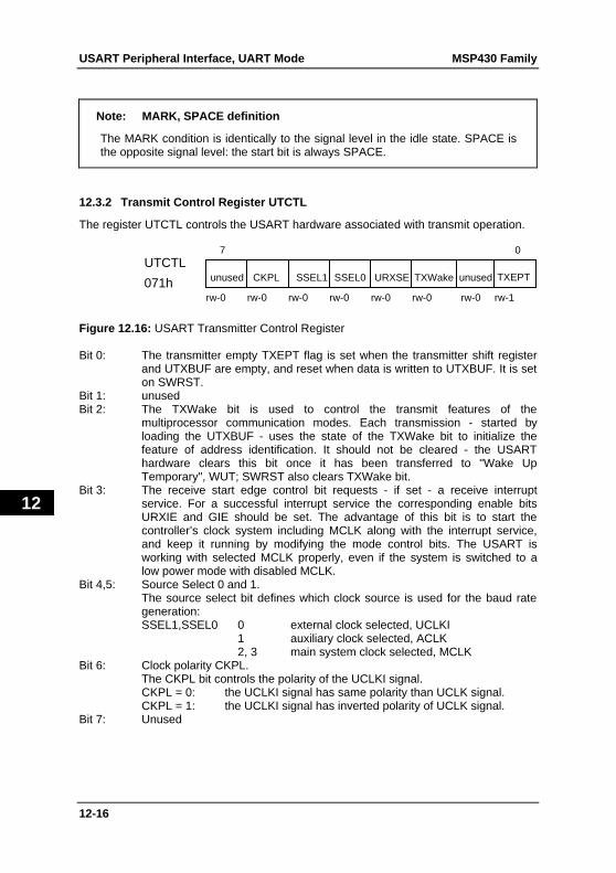
12.3.2 Transmit Control Register UTCTL
The register UTCTL controls the USART hardware associated with transmit operation.
UTCTL
rw-0 rw-0 rw-0 rw-0 rw-0 rw-0 rw-0 rw-1071h
7 0
TXEPTTXWakeURXSESSEL1CKPL SSEL0 unusedunused
Figure 12.16: USART Transmitter Control Register
Bit 0: The transmitter empty TXEPT flag is set when the transmitter shift registerand UTXBUF are empty, and reset when data is written to UTXBUF. It is seton SWRST.
Bit 1: unusedBit 2: The TXWake bit is used to control the transmit features of the
multiprocessor communication modes. Each transmission - started byloading the UTXBUF - uses the state of the TXWake bit to initialize thefeature of address identification. It should not be cleared - the USARThardware clears this bit once it has been transferred to "Wake UpTemporary", WUT; SWRST also clears TXWake bit.
Bit 3: The receive start edge control bit requests - if set - a receive interruptservice. For a successful interrupt service the corresponding enable bitsURXIE and GIE should be set. The advantage of this bit is to start thecontroller’s clock system including MCLK along with the interrupt service,and keep it running by modifying the mode control bits. The USART isworking with selected MCLK properly, even if the system is switched to alow power mode with disabled MCLK.
Bit 4,5: Source Select 0 and 1.The source select bit defines which clock source is used for the baud rategeneration:SSEL1,SSEL0 0 external clock selected, UCLKI
1 auxiliary clock selected, ACLK2, 3 main system clock selected, MCLK
Bit 6: Clock polarity CKPL.The CKPL bit controls the polarity of the UCLKI signal.CKPL = 0: the UCLKI signal has same polarity than UCLK signal.CKPL = 1: the UCLKI signal has inverted polarity of UCLK signal.
Bit 7: Unused
MSP430 Family USART Peripheral Interface, UART Mode
12-17
12
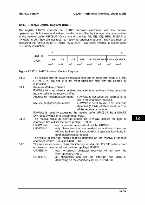
12.3.3 Receive Control Register URCTL
The register URCTL controls the USART hardware associated with the receiveroperation and holds error and wakeup conditions modified by the latest character writtento the receive buffer URXBUF. Once any of the bits FE, PE, OE, BRK, RXERR orRXWake is set, they are not reset by receiving another character. They are reset byaccessing the receive buffer URXBUF, by a USART SW reset SWRST, a system resetPUC or by instruction.
URCTL
rw-0 rw-0 rw-0 rw-0 rw-0 rw-0 rw-0 rw-0072h
7 0
RXERRRXWakeOEPEFE BRK URXEIE URXWIE
Figure 12.17: USART Receiver Control Register
Bit 0: The receive error bit RXERR indicates that one or more error flags (FE, PE,OE or BRK) are set. It is not reset when the error bits are cleared byinstruction.
Bit 1: Receiver Wake-up DetectRXWake bit is set when a received character is an address character and istransferred into the receive buffer.Address bit multiprocessor mode: RXWake is set when the address bit is
set in the character received.Idle line multiprocessor mode: RXWake is set if an idle URXD line was
detected (11 bits of Mark level) in frontof the received character.
RXWake is reset by accessing the receive buffer URXBUF, by a USARTSW reset SWRST or a system reset PUC.
Bit 2: The receive wake-up interrupt enable bit URXWIE selects the type ofcharacter that will set the interrupt flag URXIFG:URXWIE=0: each character received will set the URXIFGURXWIE=1: only characters that are marked as address characters
will set the interrupt flag URXIFG. It operates identically inboth multiprocessor modes.
The wake-up interrupt enable feature depends on the receive erroneouscharacter feature. See also URXEIE bit.
Bit 3: The receive erroneous character interrupt enable bit URXEIE selects if anerroneous character will set the interrupt flag URXIFG.URXEIE=0: each erroneous character received will not alter the
interrupt flag URXIFGURXEIE=1: all characters can set the interrupt flag URXIFG
depending on the conditions set by URXWIE bit.
USART Peripheral Interface, UART Mode MSP430 Family
12-18
12
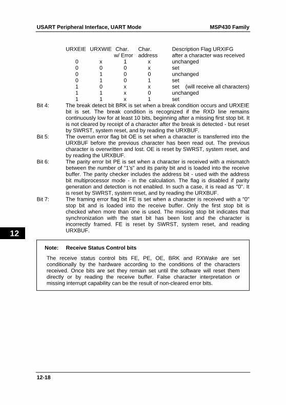
URXEIE URXWIE Char. Char. Description Flag URXIFGw/ Error address after a character was received
0 x 1 x unchanged0 0 0 x set0 1 0 0 unchanged0 1 0 1 set1 0 x x set (will receive all characters)1 1 x 0 unchanged1 1 x 1 set
Bit 4: The break detect bit BRK is set when a break condition occurs and URXEIEbit is set. The break condition is recognized if the RXD line remainscontinuously low for at least 10 bits, beginning after a missing first stop bit. Itis not cleared by receipt of a character after the break is detected - but resetby SWRST, system reset, and by reading the URXBUF.
Bit 5: The overrun error flag bit OE is set when a character is transferred into theURXBUF before the previous character has been read out. The previouscharacter is overwritten and lost. OE is reset by SWRST, system reset, andby reading the URXBUF.
Bit 6: The parity error bit PE is set when a character is received with a mismatchbetween the number of "1's" and its parity bit and is loaded into the receivebuffer. The parity checker includes the address bit - used with the addressbit multiprocessor mode - in the calculation. The flag is disabled if paritygeneration and detection is not enabled. In such a case, it is read as "0". Itis reset by SWRST, system reset, and by reading the URXBUF.
Bit 7: The framing error flag bit FE is set when a character is received with a "0"stop bit and is loaded into the receive buffer. Only the first stop bit ischecked when more than one is used. The missing stop bit indicates thatsynchronization with the start bit has been lost and the character isincorrectly framed. FE is reset by SWRST, system reset, and readingURXBUF.
Note: Receive Status Control bits
The receive status control bits FE, PE, OE, BRK and RXWake are setconditionally by the hardware according to the conditions of the charactersreceived. Once bits are set they remain set until the software will reset themdirectly or by reading the receive buffer. False character interpretation ormissing interrupt capability can be the result of non-cleared error bits.
MSP430 Family USART Peripheral Interface, UART Mode
12-19
12
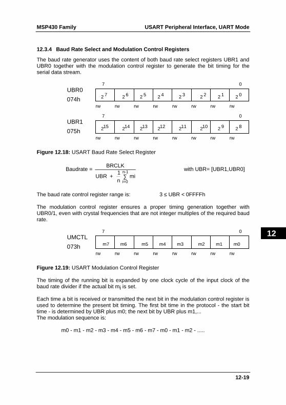
12.3.4 Baud Rate Select and Modulation Control Registers
The baud rate generator uses the content of both baud rate select registers UBR1 andUBR0 together with the modulation control register to generate the bit timing for theserial data stream.
UBR0
rw rw rw rw rw rw rw rw074h
7 0
2
UBR1
rw rw rw rw rw rw rw rw075h
7 0
7 2 6 2 5 2 4 2 3 2 2 2 1 2 0
215 214 213 212 211 210 2 9 2 8
Figure 12.18: USART Baud Rate Select Register
Baudrate = BRCLK
UBR + 1n
mii=0
n-1∑
with UBR= [UBR1,UBR0]
The baud rate control register range is: 3 ≤ UBR < 0FFFFh
The modulation control register ensures a proper timing generation together withUBR0/1, even with crystal frequencies that are not integer multiples of the required baudrate.
UMCTL
rw rw rw rw rw rw rw rw073h
7 0
m7 m6 m4 m3 m2 m1 m0m5
Figure 12.19: USART Modulation Control Register
The timing of the running bit is expanded by one clock cycle of the input clock of thebaud rate divider if the actual bit mi is set.
Each time a bit is received or transmitted the next bit in the modulation control register isused to determine the present bit timing. The first bit time in the protocol - the start bittime - is determined by UBR plus m0; the next bit by UBR plus m1,...The modulation sequence is:
m0 - m1 - m2 - m3 - m4 - m5 - m6 - m7 - m0 - m1 - m2 - .....
USART Peripheral Interface, UART Mode MSP430 Family
12-20
12
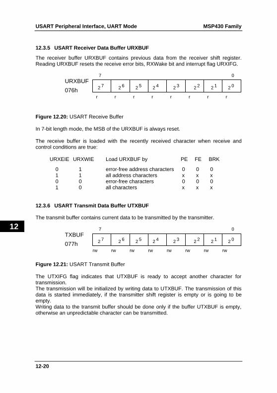
12.3.5 USART Receiver Data Buffer URXBUF
The receiver buffer URXBUF contains previous data from the receiver shift register.Reading URXBUF resets the receive error bits, RXWake bit and interrupt flag URXIFG.
URXBUF
r r r r r r r r076h
7 0
2 7 2 6 2 5 2 4 2 3 2 2 2 1 2 0
Figure 12.20: USART Receive Buffer
In 7-bit length mode, the MSB of the URXBUF is always reset.
The receive buffer is loaded with the recently received character when receive andcontrol conditions are true:
URXEIE URXWIE Load URXBUF by PE FE BRK
0 1 error-free address characters 0 0 0 1 1 all address characters x x x 0 0 error-free characters 0 0 0 1 0 all characters x x x
12.3.6 USART Transmit Data Buffer UTXBUF
The transmit buffer contains current data to be transmitted by the transmitter.
TXBUF
rw rw rw rw rw rw rw rw077h
7 0
2 7 2 6 2 5 2 4 2 3 2 2 2 1 2 0
Figure 12.21: USART Transmit Buffer
The UTXIFG flag indicates that UTXBUF is ready to accept another character fortransmission.The transmission will be initialized by writing data to UTXBUF. The transmission of thisdata is started immediately, if the transmitter shift register is empty or is going to beempty.Writing data to the transmit buffer should be done only if the buffer UTXBUF is empty,otherwise an unpredictable character can be transmitted.
MSP430 Family USART Peripheral Interface, UART Mode
12-21
12
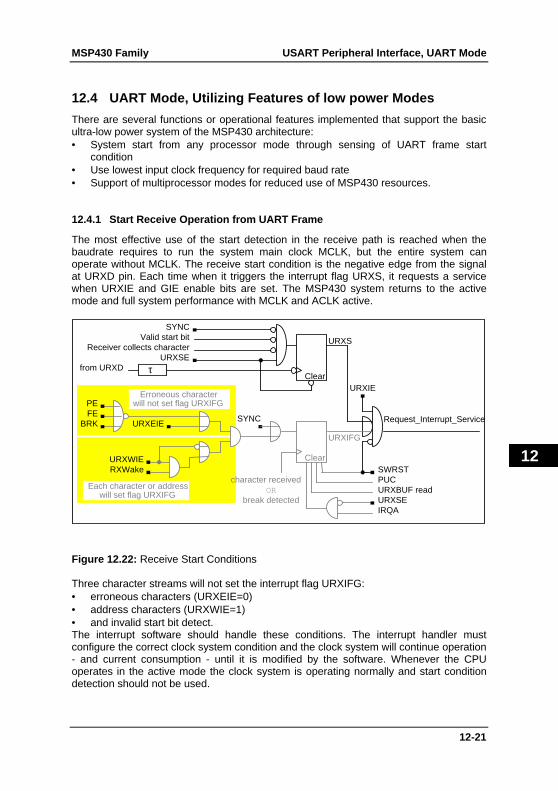
12.4 UART Mode, Utilizing Features of low power Modes
There are several functions or operational features implemented that support the basicultra-low power system of the MSP430 architecture:• System start from any processor mode through sensing of UART frame start
condition• Use lowest input clock frequency for required baud rate• Support of multiprocessor modes for reduced use of MSP430 resources.
12.4.1 Start Receive Operation from UART Frame
The most effective use of the start detection in the receive path is reached when thebaudrate requires to run the system main clock MCLK, but the entire system canoperate without MCLK. The receive start condition is the negative edge from the signalat URXD pin. Each time when it triggers the interrupt flag URXS, it requests a servicewhen URXIE and GIE enable bits are set. The MSP430 system returns to the activemode and full system performance with MCLK and ACLK active.
URXIE
URXIFG
PUCSWRST
URXBUF read
IRQA
Clear
Request_Interrupt_Service
ORbreak detected
URXS
Clear
URXSEfrom URXD
Receiver collects characterValid start bit
τ
SYNC
URXEIE
URXWIERXWake
Erroneous characterwill not set flag URXIFG
character receivedEach character or address
will set flag URXIFGURXSE
SYNC
PEFE
BRK
Figure 12.22: Receive Start Conditions
Three character streams will not set the interrupt flag URXIFG:• erroneous characters (URXEIE=0)• address characters (URXWIE=1)• and invalid start bit detect.The interrupt software should handle these conditions. The interrupt handler mustconfigure the correct clock system condition and the clock system will continue operation- and current consumption - until it is modified by the software. Whenever the CPUoperates in the active mode the clock system is operating normally and start conditiondetection should not be used.
USART Peripheral Interface, UART Mode MSP430 Family
12-22
12
Start conditions
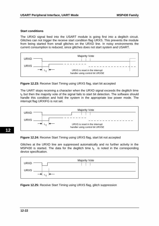
The URXD signal feed into the USART module is going first into a deglitch circuit.Glitches can not trigger the receive start condition flag URXS. This prevents the modulefrom being started from small glitches on the URXD line. In noisy environments thecurrent consumption is reduced, since glitches does not start system and USART.
URXD
τt
Majority Vote
URXS
URXS is reset in the interrupthandler using control bit URXSE
Figure 12.23: Receive Start Timing using URXS flag, start bit accepted
The UART stops receiving a character when the URXD signal exceeds the deglitch timetτ but then the majority vote of the signal fails to start bit detection. The software shouldhandle this condition and hold the system in the appropriate low power mode. Theinterrupt flag URXIFG is not set.
URXD
τt
Majority Vote
URXS
URXS is reset in the interrupthandler using control bit URXSE
Figure 12.24: Receive Start Timing using URXS flag, start bit not accepted
Glitches at the URXD line are suppressed automatically and no further activity in theMSP430 is started. The data for the deglitch time tτ is noted in the correspondingdevice specification.
URXD
τt
Majority Vote
URXS
Figure 12.25: Receive Start Timing using URXS flag, glitch suppression
MSP430 Family USART Peripheral Interface, UART Mode
12-23
12
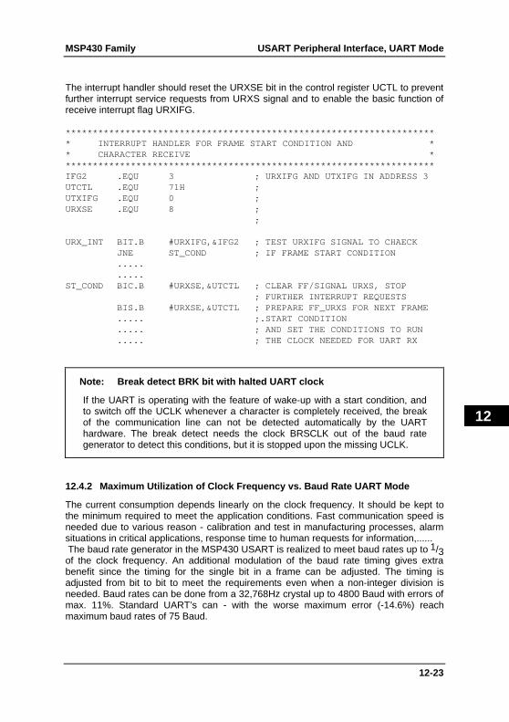
The interrupt handler should reset the URXSE bit in the control register UCTL to preventfurther interrupt service requests from URXS signal and to enable the basic function ofreceive interrupt flag URXIFG.
********************************************************************* INTERRUPT HANDLER FOR FRAME START CONDITION AND ** CHARACTER RECEIVE *********************************************************************IFG2 .EQU 3 ; URXIFG AND UTXIFG IN ADDRESS 3UTCTL .EQU 71H ;UTXIFG .EQU 0 ;URXSE .EQU 8 ;
;
URX_INT BIT.B #URXIFG,&IFG2 ; TEST URXIFG SIGNAL TO CHAECKJNE ST_COND ; IF FRAME START CONDITION..........
ST_COND BIC.B #URXSE,&UTCTL ; CLEAR FF/SIGNAL URXS, STOP; FURTHER INTERRUPT REQUESTS
BIS.B #URXSE,&UTCTL ; PREPARE FF_URXS FOR NEXT FRAME..... ;.START CONDITION..... ; AND SET THE CONDITIONS TO RUN..... ; THE CLOCK NEEDED FOR UART RX
Note: Break detect BRK bit with halted UART clock
If the UART is operating with the feature of wake-up with a start condition, andto switch off the UCLK whenever a character is completely received, the breakof the communication line can not be detected automatically by the UARThardware. The break detect needs the clock BRSCLK out of the baud rategenerator to detect this conditions, but it is stopped upon the missing UCLK.
12.4.2 Maximum Utilization of Clock Frequency vs. Baud Rate UART Mode
The current consumption depends linearly on the clock frequency. It should be kept tothe minimum required to meet the application conditions. Fast communication speed isneeded due to various reason - calibration and test in manufacturing processes, alarmsituations in critical applications, response time to human requests for information,...... The baud rate generator in the MSP430 USART is realized to meet baud rates up to 1/3of the clock frequency. An additional modulation of the baud rate timing gives extrabenefit since the timing for the single bit in a frame can be adjusted. The timing isadjusted from bit to bit to meet the requirements even when a non-integer division isneeded. Baud rates can be done from a 32,768Hz crystal up to 4800 Baud with errors ofmax. 11%. Standard UART’s can - with the worse maximum error (-14.6%) reachmaximum baud rates of 75 Baud.
USART Peripheral Interface, UART Mode MSP430 Family
12-24
12
12.4.3 Support of multiprocessor modes for reduced use of MSP430 resources
Communication systems with multiple character protocols can use the features ofmultiprocessor modes - whether the idle line or the address bit protocol. The firstcharacter can be a target address, a message identifier or can have another definition.This character is interpreted by software, and if there is any significance for theapplication the succeeding characters are collected and further activities defined. Nosignificance of the first character would stop any activity for the processing device. Theapplication of this feature is supported by the wake-up interrupt feature in receivesituation, and to send wake-up conditions along with transmission. Avoiding activity oncharacters without any significance reduces the use of MSP430 resources and thesystem can remain in the most efficient power conserving mode.Additional to the multiprocessor modes, rejection of erroneous characters avoidsinterrupt handling of these characters. This is useful whenever erroneous characters willnot be processed anyway. The processor waits in the most efficient power conservingmode until a character can be processed.
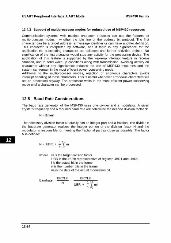
12.5 Baud Rate Considerations
The baud rate generator of the MSP430 uses one divider and a modulator. A givencrystal’s frequency and a required baud rate will determine the needed division factor N:
N = Error!
The necessary division factor N usually has an integer part and a fraction. The divider inthe baudrate generator realizes the integer portion of the division factor N and themodulator is responsible for meeting the fractional part as close as possible. The factorN is defined:
N = UBR + 1n
mii=0
n-1∑
where N is the target division factorUBR is the 16-bit representative of register UBR1 and UBR0i is the actual bit in the framen is the number bits in the framemi is the data of the actual modulation bit.
Baudrate = BRCLK
N =
BRCLK
UBR + 1n
mii=0
n-1∑
MSP430 Family USART Peripheral Interface, UART Mode
12-25
12
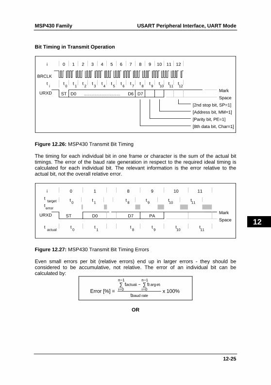
Bit Timing in Transmit Operation
[Address bit, MM=1]
[Parity bit, PE=1]
D0
[8th data bit, Char=1]
ST D7D6..............................
[2nd stop bit, SP=1]
Mark
Space
BRCLK
URXD
0t
1t
2t
3t
4t
5t
6t
7t
8t
9t
10t
11t
12t
it
0 1 2 3 4 5 6 7 8 9 10 11 12i
Figure 12.26: MSP430 Transmit Bit Timing
The timing for each individual bit in one frame or character is the sum of the actual bittimings. The error of the baud rate generation in respect to the required ideal timing iscalculated for each individual bit. The relevant information is the error relative to theactual bit, not the overall relative error.
D0ST PAD7Mark
SpaceURXD
targett
0 1 8 9 10 11i
0t
1t
8 9t
10t
11tt
actualt
0t
1t
8 9t
10t
11tt
errort
Figure 12.27: MSP430 Transmit Bit Timing Errors
Even small errors per bit (relative errors) end up in larger errors - they should beconsidered to be accumulative, not relative. The error of an individual bit can becalculated by:
Error [%] = t t
tx
actual t eti
n
i
n
baud rate
i i−=
−
=
−∑∑ arg
0
1
0
1
100%
OR
USART Peripheral Interface, UART Mode MSP430 Family
12-26
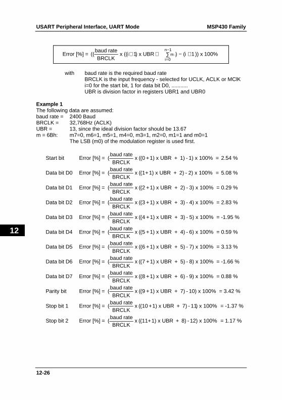
12
Error [%] = (( (( ) ) ( ))baud rateBRCLK
x i x UBR i xmi
ni+ + ∑ − +
=
−1 1 100%
0
1
with baud rate is the required baud rateBRCLK is the input frequency - selected for UCLK, ACLK or MClKi=0 for the start bit, 1 for data bit D0, ...........UBR is division factor in registers UBR1 and UBR0
Example 1The following data are assumed:baud rate = 2400 BaudBRCLK = 32,768Hz (ACLK)UBR = 13, since the ideal division factor should be 13.67m = 6Bh: m7=0, m6=1, m5=1, m4=0, m3=1, m2=0, m1=1 and m0=1
The LSB (m0) of the modulation register is used first.
Start bit Error [%] = (baud rate
BRCLKx (0 +1) x UBR + 1) - 1) x 100% ( = 2.54 %
Data bit D0 Error [%] = (baud rateBRCLK
x (1+1) x UBR + 2) - 2) x 100% ( = 5.08 %
Data bit D1 Error [%] = (baud rateBRCLK
x (2 +1) x UBR + 2) - 3) x 100% ( = 0.29 %
Data bit D2 Error [%] = (baud rateBRCLK
x (3 +1) x UBR + 3) - 4) x 100% ( = 2.83 %
Data bit D3 Error [%] = (baud rateBRCLK
x (4 +1) x UBR + 3) - 5) x 100% ( = -1.95 %
Data bit D4 Error [%] = (baud rateBRCLK
x (5 +1) x UBR + 4) - 6) x 100% ( = 0.59 %
Data bit D5 Error [%] = (baud rateBRCLK
x (6 +1) x UBR + 5) - 7) x 100% ( = 3.13 %
Data bit D6 Error [%] = (baud rateBRCLK
x (7 +1) x UBR + 5) - ) x 100% ( 8 = -1.66 %
Data bit D7 Error [%] = (baud rateBRCLK
x (8 +1) x UBR + 6) - ) x 100% ( 9 = 0.88 %
Parity bit Error [%] = (baud rateBRCLK
x (9 +1) x UBR + 7) - ) x 100% ( 10 = 3.42 %
Stop bit 1 Error [%] = (baud rateBRCLK
x (10 +1) x UBR + 7) - ) x 100% ( 11 = -1.37 %
Stop bit 2 Error [%] = (baud rateBRCLK
x (11+1) x UBR + 8) - ) x 100% ( 12 = 1.17 %
MSP430 Family USART Peripheral Interface, UART Mode
12-27
12
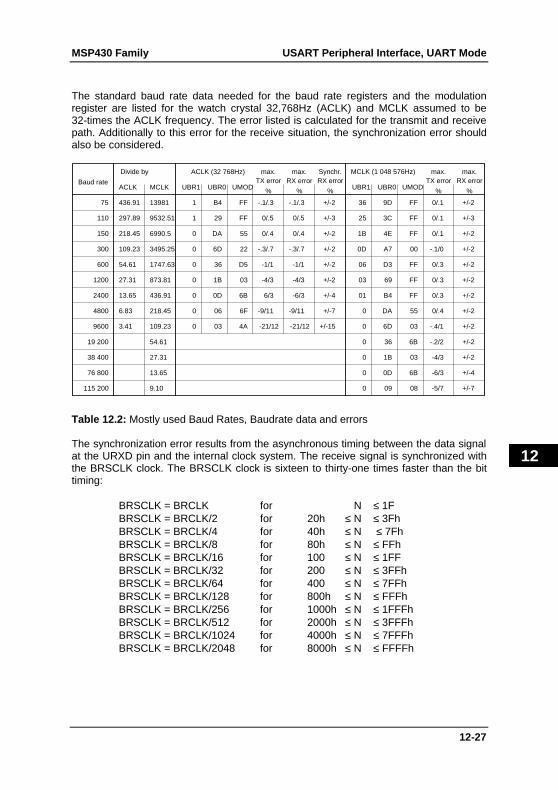
The standard baud rate data needed for the baud rate registers and the modulationregister are listed for the watch crystal 32,768Hz (ACLK) and MCLK assumed to be32-times the ACLK frequency. The error listed is calculated for the transmit and receivepath. Additionally to this error for the receive situation, the synchronization error shouldalso be considered.
Baud rateUBR1
Divide by
UBR0 UMOD
75
110
150
300
600
1200
2400
4800
9600
19 200
38 400
76 800
115 200
ACLK MCLK
436.91
297.89
218.45
109.23
54.61
27.31
13.65
6.83
3.41
13981
9532.51
6990.5
3495.25
1747.63
873.81
436.91
218.45
109.23
54.61
27.31
13.65
9.10
ACLK (32 768Hz)
UBR1 UBR0 UMOD
MCLK (1 048 576Hz)TX error
max.TX error
max.
1 B4
1 29
0 DA
0 6D
0 36
0 1B
0 0D
0 06
0 03
01 B4
03 69
0 DA
0 6D
0 36
0 1B
0 09
36 9D
25 3C
1B 4E
0D A7
06 D3
0 0D
FF
FF
55
22
D5
03
6B
6F
4A
-9/11
6/3
-4/3
-1/1
-.3/.7
0/.4
0/.5
-.1/.3
-21/12
FF
FF
55
03
6B
03
08
FF
FF
FF
00
FF
6B
0/.3
0/.3
0/.4
-.4/1
-.2/2
-4/3
-5/7
-6/3
0/.3
-.1/0
0/.1
0/.1
0/.1
RX errormax.
-9/11
-6/3
-4/3
-1/1
-.3/.7
0/.4
0/.5
-.1/.3
-21/12
RX errormax.
RX errorSynchr.
+/-15
+/-7
+/-4
+/-2
+/-2
+/-2
+/-2
+/-3
+/-2
+/-7
+/-4
+/-2
+/-2
+/-2
+/-2
+/-2
+/-2
+/-2
+/-2
+/-3
+/-2
+/-2
%% % %%
Table 12.2: Mostly used Baud Rates, Baudrate data and errors
The synchronization error results from the asynchronous timing between the data signalat the URXD pin and the internal clock system. The receive signal is synchronized withthe BRSCLK clock. The BRSCLK clock is sixteen to thirty-one times faster than the bittiming:
BRSCLK = BRCLK for N ≤ 1FBRSCLK = BRCLK/2 for 20h ≤ N ≤ 3FhBRSCLK = BRCLK/4 for 40h ≤ N ≤ 7FhBRSCLK = BRCLK/8 for 80h ≤ N ≤ FFhBRSCLK = BRCLK/16 for 100 ≤ N ≤ 1FFBRSCLK = BRCLK/32 for 200 ≤ N ≤ 3FFhBRSCLK = BRCLK/64 for 400 ≤ N ≤ 7FFhBRSCLK = BRCLK/128 for 800h ≤ N ≤ FFFhBRSCLK = BRCLK/256 for 1000h ≤ N ≤ 1FFFhBRSCLK = BRCLK/512 for 2000h ≤ N ≤ 3FFFhBRSCLK = BRCLK/1024 for 4000h ≤ N ≤ 7FFFhBRSCLK = BRCLK/2048 for 8000h ≤ N ≤ FFFFh
USART Peripheral Interface, UART Mode MSP430 Family
12-28
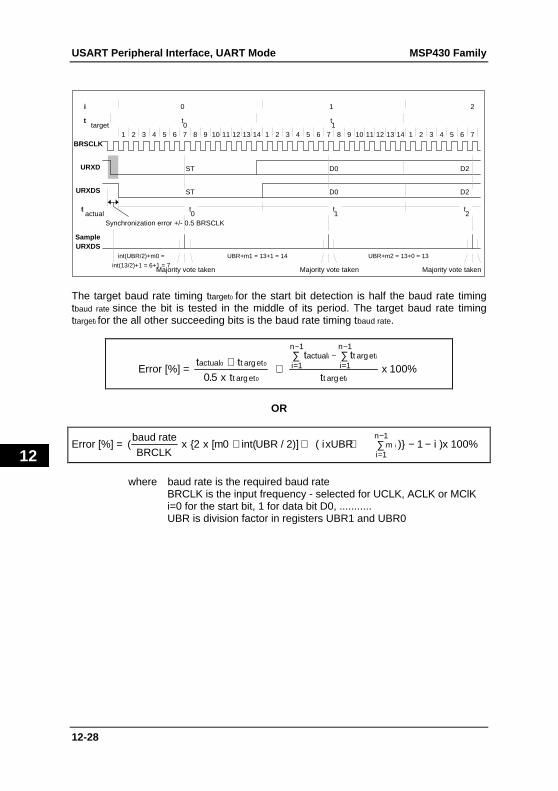
12
ST D0URXD
targett
0 1i
actualt
0t
1t
0t
1t
BRSCLK
ST D0URXDS
Synchronization error +/- 0.5 BRSCLK
SampleURXDS
1 2 3 4 5 6 7 8 9 10 11 12 13 14 1 2 3 4 5 6 7 8 9 10 11 12 13 14 1 2 3 4 5 6
int(UBR/2)+m0 = UBR+m1 = 13+1 = 14
D2
D2
7
UBR+m2 = 13+0 = 13
2t
2
Majority vote taken Majority vote taken Majority vote takenint(13/2)+1 = 6+1 = 7
The target baud rate timing ttarget0 for the start bit detection is half the baud rate timingtbaud rate since the bit is tested in the middle of its period. The target baud rate timingttargeti for the all other succeeding bits is the baud rate timing tbaud rate.
Error [%] = t t
x t
t t
tx
actual t et
t et
actual t eti
n
i
n
t et
i i
i
0 0
00 5100%1
1
1
1
+ +∑∑ −=
−
=
−
arg
arg
arg
arg.
OR
Error [%] = ( { [ int( / )] ( )} )baud rateBRCLK
x x m UBR ixUBR i xmi
ni2 0 2 1 100%
1
1+ + + ∑ − −
=
−
where baud rate is the required baud rateBRCLK is the input frequency - selected for UCLK, ACLK or MClKi=0 for the start bit, 1 for data bit D0, ...........UBR is division factor in registers UBR1 and UBR0
MSP430 Family USART Peripheral Interface, UART Mode
12-29
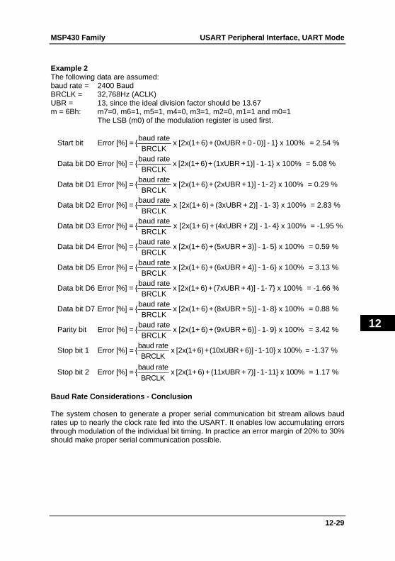
12
Example 2The following data are assumed:baud rate = 2400 BaudBRCLK = 32,768Hz (ACLK)UBR = 13, since the ideal division factor should be 13.67m = 6Bh: m7=0, m6=1, m5=1, m4=0, m3=1, m2=0, m1=1 and m0=1
The LSB (m0) of the modulation register is used first.
Start bit Error [%] = {baud rateBRCLK
x (1+ 6) + (0xUBR + 0 - 0)] - 1} x 100% [2x = 2.54 %
Data bit D0 Error [%] = {baud rateBRCLK
x (1+ 6)+ (1xUBR +1)] - 1-1} x 100% [2x = 5.08 %
Data bit D1 Error [%] = {baud rateBRCLK
x (1+ 6)+ (2xUBR +1)] - 1- 2} x 100% [2x = 0.29 %
Data bit D2 Error [%] = {baud rateBRCLK
x (1+ 6) + (3xUBR + 2)] - 1- 3} x 100% [2x = 2.83 %
Data bit D3 Error [%] = {baud rateBRCLK
x (1+ 6) + (4xUBR + 2)] - 1- 4} x 100% [2x = -1.95 %
Data bit D4 Error [%] = {baud rateBRCLK
x (1+ 6) + (5xUBR + 3)] - 1- 5} x 100% [2x = 0.59 %
Data bit D5 Error [%] = {baud rateBRCLK
x (1+ 6) + (6xUBR + 4)] - 1- 6} x 100% [2x = 3.13 %
Data bit D6 Error [%] = {baud rateBRCLK
x (1+ 6)+(7xUBR + 4)] - 1- 7} x 100% [2x = -1.66 %
Data bit D7 Error [%] = {baud rateBRCLK
x (1+ 6) + (8xUBR + 5)] - 1- 8} x 100% [2x = 0.88 %
Parity bit Error [%] = {baud rateBRCLK
x (1+ 6) + (9xUBR + 6)] - 1- 9} x 100% [2x = 3.42 %
Stop bit 1 Error [%] = {baud rateBRCLK
x (1+6)+(10xUBR+6)] -1-10} x 100% [2x = -1.37 %
Stop bit 2 Error [%] = {baud rate
BRCLKx (1+ 6) + (11xUBR + 7)] -1-11} x 100% [2x = 1.17 %
Baud Rate Considerations - Conclusion
The system chosen to generate a proper serial communication bit stream allows baudrates up to nearly the clock rate fed into the USART. It enables low accumulating errorsthrough modulation of the individual bit timing. In practice an error margin of 20% to 30%should make proper serial communication possible.
USART Peripheral Interface, UART Mode MSP430 Family
12-30
12
MSP430 Family USART Peripheral Interface, SPI Mode
13-1
13
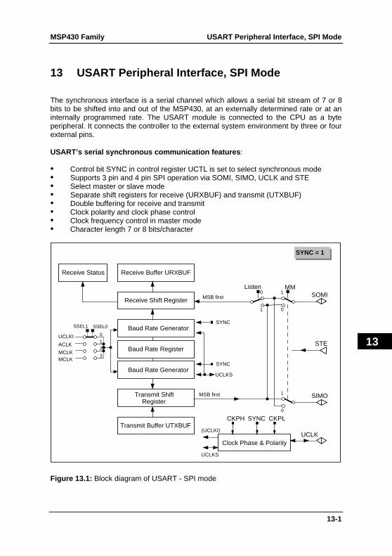
13 USART Peripheral Interface, SPI Mode
The synchronous interface is a serial channel which allows a serial bit stream of 7 or 8bits to be shifted into and out of the MSP430, at an externally determined rate or at aninternally programmed rate. The USART module is connected to the CPU as a byteperipheral. It connects the controller to the external system environment by three or fourexternal pins.
USART’s serial synchronous communication features :
• Control bit SYNC in control register UCTL is set to select synchronous mode• Supports 3 pin and 4 pin SPI operation via SOMI, SIMO, UCLK and STE• Select master or slave mode• Separate shift registers for receive (URXBUF) and transmit (UTXBUF)• Double buffering for receive and transmit• Clock polarity and clock phase control• Clock frequency control in master mode• Character length 7 or 8 bits/character
Receive Buffer URXBUF
Receive Shift Register
Baud Rate Generator
Transmit ShiftRegister
Transmit Buffer UTXBUF
Receive Status
CKPL
UCLKI
MCLK
ACLK
SSEL1 SSEL0
0
12
3MCLK
Baud Rate Generator
Baud Rate Register
Listen0 1 SOMI
1 0
1 SIMO
0
MM
UCLKClock Phase & Polarity
CKPH
(UCLKI)
UCLKS
SYNC
UCLKS
SYNC
SYNC
MSB first
SYNC = 1
MSB first
STE
Figure 13.1: Block diagram of USART - SPI mode
USART Peripheral Interface, SPI Mode MSP430 Family
13-2
13
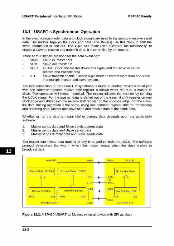
13.1 USART’s Synchronous Operation
In the synchronous mode, data and clock signals are used to transmit and receive serialdata. The master supplies the clock and data. The slave(s) use this clock to shift theserial information in and out. The 4 pin SPI mode uses a control line additionally, toenable a slave to receive and transmit data. It is controlled by the master.
Three or four signals are used for the data exchange:• SIMO Slave in, master out• SOMI Slave out, master in• UCLK USART clock, the master drives this signal and the slave uses it to
receive and transmit data• STE Slave transmit enable, used in 4-pin mode to control more than one slave
in a multiple master and slave system.
The interconnection of the USART in synchronous mode to another device’s serial portwith one common transmit receive shift register is shown when MSP430 is master orslave. The operation will remain identical. The master initiates the transfer by sendingthe UCLK signal. For the master, data is shifted out of the transmit shift register on oneclock edge and shifted into the receive shift register on the opposite edge. For the slave,the data shifting operation is the same, using one common register shift for transmittingand receiving data. Master and slave send and receive data at the same time.
Whether or not the data is meaningful or dummy data depends upon the applicationsoftware:
1. Master sends data and Slave sends dummy data2. Master sends data and Slave sends data3. Master sends dummy data and Slave sends data.
The master can initiate data transfer at any time, and controls the UCLK. The softwareprotocol determines the way in which the master knows when the slave wishes tobroadcast data.
Transmit Buffer UTXBUF
Transmit Shift Reg
Receive Buffer URXBUF
Receive Shift Reg
UCLK
SOMI
SIMO
MSP430 USART
SPI Receive Buffer
Data Shift Reg. DSR
SCLK
SOMI
SIMO
COMMON SPI
MSBLSBMSBLSBMSB LSB
MASTER SLAVE
STE
STE ..
SS
Px.x
Port.x
Figure 13.2: MSP430 USART as Master, external device with SPI as slave
MSP430 Family USART Peripheral Interface, SPI Mode
13-3
13
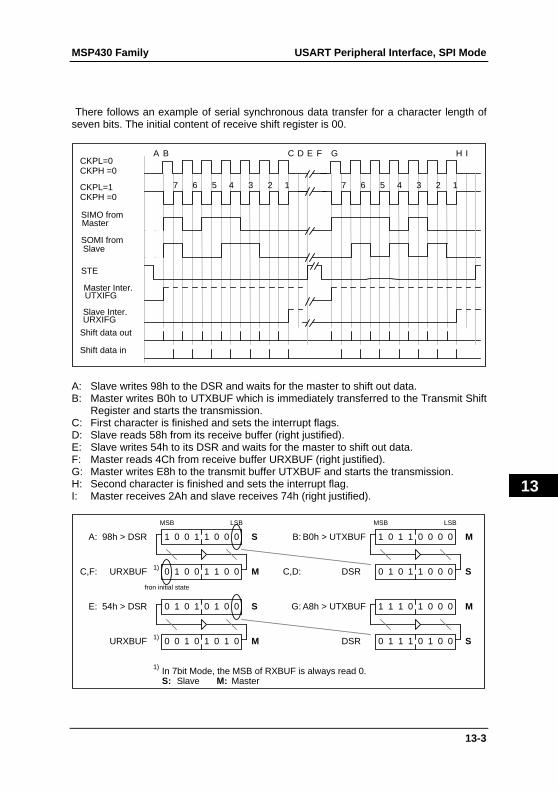
There follows an example of serial synchronous data transfer for a character length ofseven bits. The initial content of receive shift register is 00.
CKPL=0CKPH =0
SIMO from
SlaveSOMI from
Master
Master Inter.
Slave Inter.URXIFG
7 6 5 4 3 2 1
BA C D E GF H I
7 6 5 4 3 2 1
Shift data out
Shift data in
CKPL=1CKPH =0
UTXIFG
STE
A: Slave writes 98h to the DSR and waits for the master to shift out data.B: Master writes B0h to UTXBUF which is immediately transferred to the Transmit Shift
Register and starts the transmission.C: First character is finished and sets the interrupt flags.D: Slave reads 58h from its receive buffer (right justified).E: Slave writes 54h to its DSR and waits for the master to shift out data.F: Master reads 4Ch from receive buffer URXBUF (right justified).G: Master writes E8h to the transmit buffer UTXBUF and starts the transmission.H: Second character is finished and sets the interrupt flag.I: Master receives 2Ah and slave receives 74h (right justified).
1 0 0 1 1 0 0 098h > DSR 1 0 1 1 0 0 0 0B0h > UTXBUF
0URXBUF 0DSR 1 0 1 1 0 0 0
0 1 0 1 0 1 0 054h > DSR
0URXBUF 1) 0 1 0 1 0 1 0
In 7bit Mode, the MSB of RXBUF is always read 0.
1 1 1 0 1 0 0 0A8h > UTXBUF
0DSR
MSB LSB MSB LSB
1 1 1 0 1 0 0
1 0 0 1 1 0 0
B:
C,D:
A:
C,F:
E: G:
fron initial state
S
S
S
S
M
M
M
M
S: Slave M: Master
1)
1)
USART Peripheral Interface, SPI Mode MSP430 Family
13-4
13
Transmit Buffer UTXBUF
Transmit Shift Reg
Receive Buffer URXBUF
Receive Shift Reg
SPI Receive Buffer
Data Shift Reg. DSR
MSB LSBMSB LSBMSBLSB
UCLK
SOMI
SIMO
MSP430 USART
SLAVE
SCLK
SOMI
SIMOMASTER
COMMON SPI
STE
STE ..
SS
Px.x
Port.x
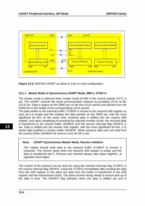
Figure 13.3: MSP430 USART as Slave in 3 pin or 4 pin configuration
13.1.1 Master Mode in Synchronous USART Mode, MM=1, SYNC=1
The master mode is selected when master mode bit MM in the control register UCTL isset. The USART controls the serial communication network by providing UCLK at theUCLK pin. Data is output on the SIMO pin on the first UCLK period and latched from theSOMI pin in the middle of the corresponding UCLK period.The data written to the transmit buffer UTXBUF is moved to the transmit shift register assoon as it is empty and this initiates the data transfer on the SIMO pin, with the mostsignificant bit first. At the same time, received data is shifted into the receive shiftregister, and upon completing of receiving the selected number of bits, the received datais transferred to the receive buffer URXBUF and the receive interrupt flag URXIFG isset. Data is shifted into the receive shift register, with the most significant bit first. It isstored right justified in receive buffer URXBUF. When previous data was not read fromthe receive buffer URXBUF the overrun error bit OE is set.
Note: USART Synchronous Master Mode, Receive initiation
The master should write data to the transmit buffer UTXBUF to receive acharacter. The receive starts when the transmit shift register is empty and thedata is transferred into it. Receive and transmit always take place together, atopposite clock edges.
The control of the protocol can be done by using the transmit interrupt flag UTXIFG orthe receive interrupt flag URXIFG. Using the UTXIFG immediately after sending the datafrom the shift register to the slave the data from the buffer is transferred to the shiftregister and the transmission starts. The slave receive timing needs to ensure pick-up ofthe data in time. The URXIFG flag indicates when the data is shifted out and in
MSP430 Family USART Peripheral Interface, SPI Mode
13-5
13
completely. The master can use URXIFG to ensure that the slave should be ready toreceive the next data properly.Any standard digital output including STE in standard digital port function can be used toselect a slave. The slave use the STE signal to enable its access to the SOMI data lineand to enable to receive the clocks on UCLK.4-pin SPI master mode, SYNC=1, STC=0, MM=1The signal on STE is used by the active master to prevent bus conflicts with anothermaster. The STE pin is input when the corresponding PnSEL bit selects the modulefunction. The master operates normally while the STE signal is high. Whenever the STEsignal is set to low - e.g. another device requests to become master - the actual masterreacts with:• the pins that drive the SPI bus lines SIMO and UCLK, are set to inputs• the error bit FE and the interrupt flag URXIFG in the URCTL register are set.The bus conflict is then removed - SIMO and UCLK do not drive the bus lines - and theerror flag indicates to the software the violation of the system integrity. The pins SIMOand UCLK are forced to inputs while STE is low, and return to the conditions defined bythe corresponding control bits when STE returns to high.In the 3-pin mode the STE input signal is not relevant for the master.
13.1.2 Slave Mode in SPI Mode, MM=0, SYNC=1
The slave mode is selected when the master mode bit MM in the control register is resetand synchronous mode is selected.
The UCLK pin is used as the input for the serial shift clock supplied by an externalmaster. The transfer rate is determined by this clock and not by the internal bit rategenerator. The data, loaded into transmit shift register via transmit buffer UTXBUFbefore start of UCLK, is transmitted on SOMI pin using the UCLK applied by the master.Simultaneously the serial data applied to SIMO pin are shifted into the receive shiftregister on the opposite edge of the clock.
The receive interrupt flag URXIFG indicates when data is received and transferred intothe receive buffer. The overrun error bit is set when previous received data is not readbefore the new data is written to the receive buffer.
4 pin SPI slave mode, SYNC=1, MM=0, STC=0In the 4 pin SPI mode the signal STE is used by the slave to enable transmit and receiveoperation. The STE signal is used to enable the receive and transmit function of theslave. It is applied from the SPI master. The receive and transmit operation is disabledwhen the STE signal is high, and enabled when it is low. Whenever the STE signalbecomes high any started receive operation is halted, and continues when the STEsignal is low again. The STE signal is used to enable one slave to access the data lines.The SOMI is input if STE is high.
USART Peripheral Interface, SPI Mode MSP430 Family
13-6
13
13.2 Interrupt and Control Function
The USART peripheral serves two main interrupt sources, the transmission and receive.Two individual interrupt vectors are available, one for receive and one for transmitinterrupt events.
The control bits of the USART are located in the SFR address range:
• Receive Interrupt Flag URXIFG initial state reset (by PUC/SWRST)• Receive Interrupt Enable URXIE initial state reset (by PUC/SWRST)• Receive Enable URXE initial state reset (by PUC)• Transmit Interrupt Flag UTXIFG initial state set (by PUC/SWRST)• Transmit Interrupt Enable UTXIE initial state reset (by PUC/SWRST)• Transmit Enable UTXE initial state reset (by PUC)
The receiver and transmitter of the USART operate in parallel and use the same baudrate generator in synchronous master mode. In synchronous slave mode the externalclock - applied to UCLK - is used for receiver and transmitter.
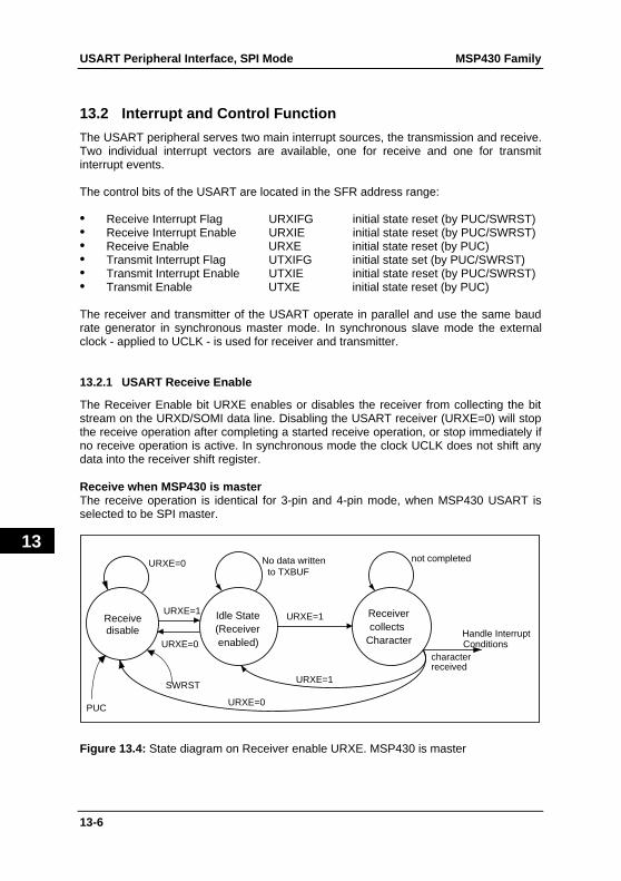
13.2.1 USART Receive Enable
The Receiver Enable bit URXE enables or disables the receiver from collecting the bitstream on the URXD/SOMI data line. Disabling the USART receiver (URXE=0) will stopthe receive operation after completing a started receive operation, or stop immediately ifno receive operation is active. In synchronous mode the clock UCLK does not shift anydata into the receiver shift register.
Receive when MSP430 is masterThe receive operation is identical for 3-pin and 4-pin mode, when MSP430 USART isselected to be SPI master.
Idle State(Receiverenabled)
Receivedisable
Receivercollects
Character
URXE=0
URXE=1
URXE=0
URXE=0
not completed
Handle InterruptConditions
characterreceived
URXE=1
URXE=1
No data writtento TXBUF
PUC
SWRST
Figure 13.4: State diagram on Receiver enable URXE. MSP430 is master
MSP430 Family USART Peripheral Interface, SPI Mode
13-7
13
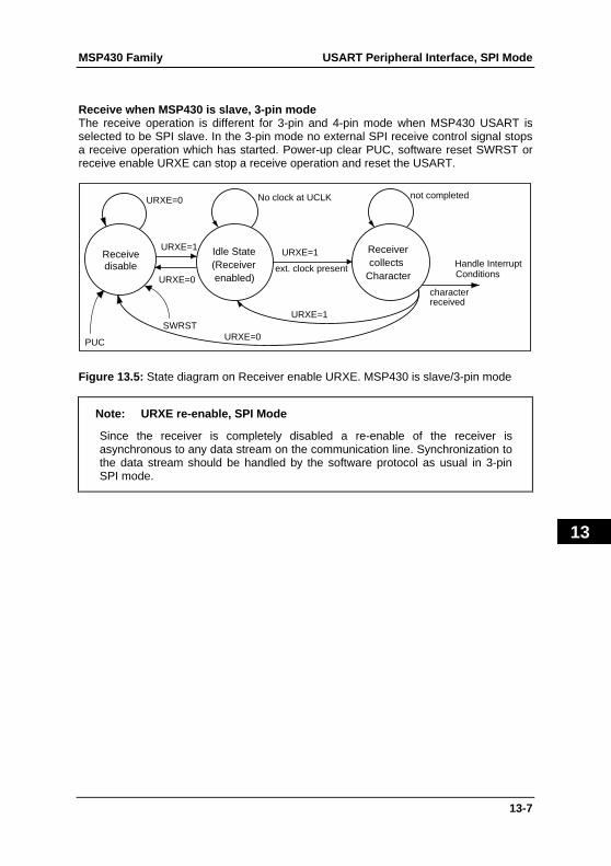
Receive when MSP430 is slave, 3-pin modeThe receive operation is different for 3-pin and 4-pin mode when MSP430 USART isselected to be SPI slave. In the 3-pin mode no external SPI receive control signal stopsa receive operation which has started. Power-up clear PUC, software reset SWRST orreceive enable URXE can stop a receive operation and reset the USART.
Idle State(Receiverenabled)
Receivedisable
Receivercollects
Character
URXE=0
URXE=1
URXE=0
URXE=0
not completed
Handle InterruptConditions
characterreceived
URXE=1
URXE=1
No clock at UCLK
ext. clock present
PUC
SWRST
Figure 13.5: State diagram on Receiver enable URXE. MSP430 is slave/3-pin mode
Note: URXE re-enable, SPI Mode
Since the receiver is completely disabled a re-enable of the receiver isasynchronous to any data stream on the communication line. Synchronization tothe data stream should be handled by the software protocol as usual in 3-pinSPI mode.
USART Peripheral Interface, SPI Mode MSP430 Family
13-8
13
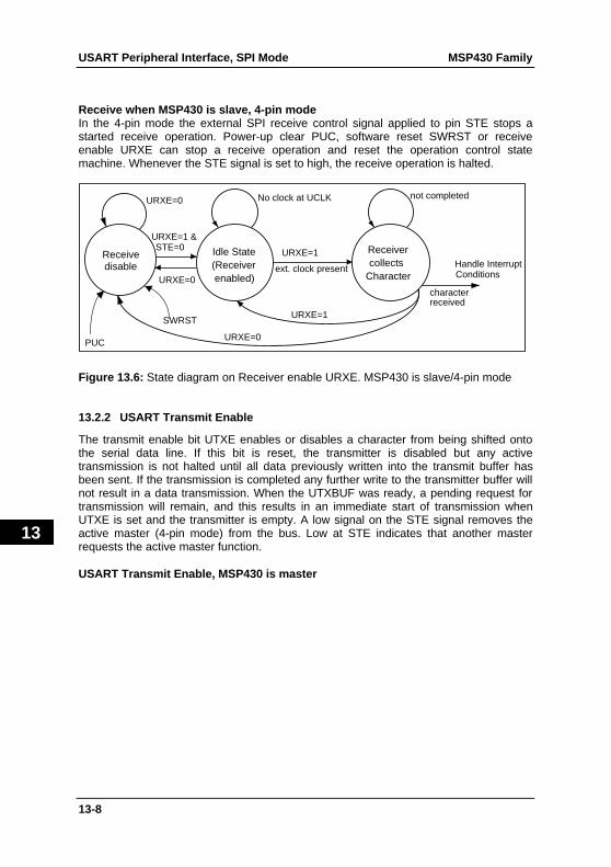
Receive when MSP430 is slave, 4-pin modeIn the 4-pin mode the external SPI receive control signal applied to pin STE stops astarted receive operation. Power-up clear PUC, software reset SWRST or receiveenable URXE can stop a receive operation and reset the operation control statemachine. Whenever the STE signal is set to high, the receive operation is halted.
Idle State(Receiverenabled)
Receivedisable
Receivercollects
Character
URXE=0
STE=0
URXE=0
URXE=0
not completed
Handle InterruptConditions
characterreceived
URXE=1
URXE=1
No clock at UCLK
ext. clock present
PUC
SWRST
URXE=1 &
Figure 13.6: State diagram on Receiver enable URXE. MSP430 is slave/4-pin mode
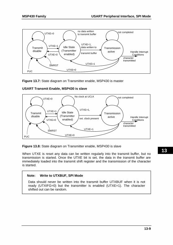
13.2.2 USART Transmit Enable
The transmit enable bit UTXE enables or disables a character from being shifted ontothe serial data line. If this bit is reset, the transmitter is disabled but any activetransmission is not halted until all data previously written into the transmit buffer hasbeen sent. If the transmission is completed any further write to the transmitter buffer willnot result in a data transmission. When the UTXBUF was ready, a pending request fortransmission will remain, and this results in an immediate start of transmission whenUTXE is set and the transmitter is empty. A low signal on the STE signal removes theactive master (4-pin mode) from the bus. Low at STE indicates that another masterrequests the active master function.
USART Transmit Enable, MSP430 is master
MSP430 Family USART Peripheral Interface, SPI Mode
13-9
13
Idle State(Transmitter
enabled)
Transmitdisable
Transmissionactive
UTXE=0
UTXE=1
UTXE=0
no data writtento transmit buffer
data written to
UTXE=0
not completed
Handle InterruptConditions
charactertransmitted
UTXE=1,
UTXE=1
transmit buffer
PUC
SWRST
Figure 13.7: State diagram on Transmitter enable, MSP430 is master
USART Transmit Enable, MSP430 is slave
Idle State(Transmitter
enabled)
Transmitdisable
Transmissionactive
UTXE=0
UTXE=1
UTXE=0
No clock at UCLK
UTXE=0
not completed
Handle InterruptConditions
charactertransmitted
UTXE=1,
UTXE=1
ext. clock present
PUC
SWRST
Figure 13.8: State diagram on Transmitter enable, MSP430 is slave
When UTXE is reset any data can be written regularly into the transmit buffer, but notransmission is started. Once the UTXE bit is set, the data in the transmit buffer areimmediately loaded into the transmit shift register and the transmission of the characteris started.
Note: Write to UTXBUF, SPI Mode
Data should never be written into the transmit buffer UTXBUF when it is notready (UTXIFG=0) but the transmitter is enabled (UTXE=1). The charactershifted out can be random.
USART Peripheral Interface, SPI Mode MSP430 Family
13-10
13
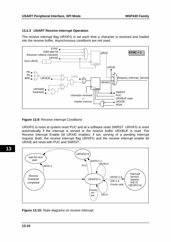
13.2.3 USART Receive Interrupt Operation
The receive interrupt flag URXIFG is set each time a character is received and loadedinto the receive buffer. Asynchronous conditions are not used.
URXIE
URXIFG
PUCSWRST
URXBUF read
IRQA
Clear
Request_Interrupt_Service
OR
master overrun
URXS
Clear
URXSEfrom URXD
Receiver collects characterValid start bit
τ
SYNC
URXEIE
URXWIERXWAKE
character received
URXSE
SYNC = 1
SYNC
PEFE
BRK
Figure 13.9: Receive Interrupt Conditions
URXIFG is reset at system reset PUC and at a software reset SWRST. URXIFG is resetautomatically if the interrupt is served or the receive buffer URXBUF is read. TheReceive Interrupt Enable bit URXIE enables, if set, serving of a pending interruptrequest. Both, the receive interrupt flag URXIFG and the receive interrupt enable bitURXIE are reset with PUC and SWRST.
URXIFG=0
started,GIE=0
URXIFG=0
wait for nextstart
Interruptservice
URXIFG=1Receive
Charactercompleted
URXE=1 PUCURXIE=0
GIE=0
Prioritytoolow
SWRST=1
URXIE=1 &
GIE=1 &
Priority valid
Figure 13.10: State diagrams on receive interrupt
MSP430 Family USART Peripheral Interface, SPI Mode
13-11
13
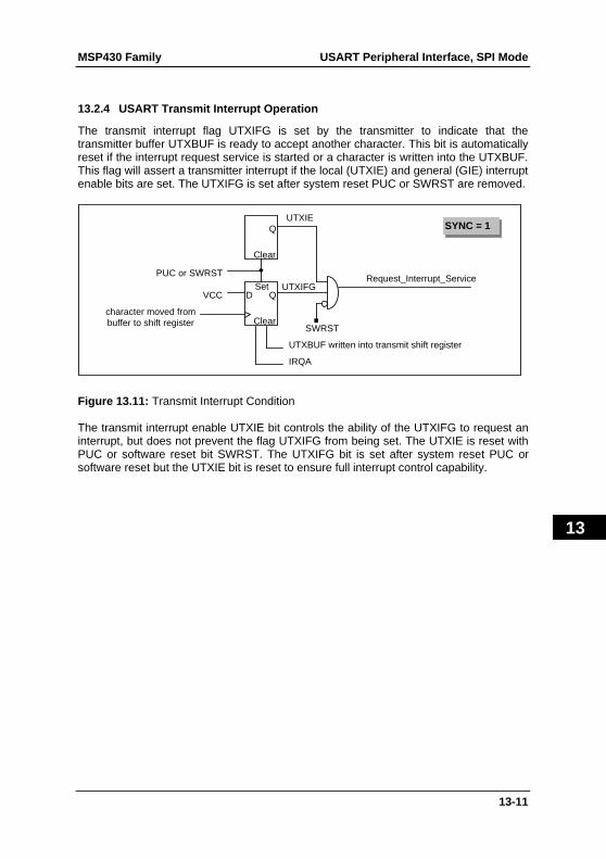
13.2.4 USART Transmit Interrupt Operation
The transmit interrupt flag UTXIFG is set by the transmitter to indicate that thetransmitter buffer UTXBUF is ready to accept another character. This bit is automaticallyreset if the interrupt request service is started or a character is written into the UTXBUF.This flag will assert a transmitter interrupt if the local (UTXIE) and general (GIE) interruptenable bits are set. The UTXIFG is set after system reset PUC or SWRST are removed.
UTXIE
UTXIFG
PUC or SWRST
UTXBUF written into transmit shift register
IRQA
character moved fromClear
Request_Interrupt_Service
buffer to shift register
VCCSet
D Q
Clear
Q
SWRST
SYNC = 1
Figure 13.11: Transmit Interrupt Condition
The transmit interrupt enable UTXIE bit controls the ability of the UTXIFG to request aninterrupt, but does not prevent the flag UTXIFG from being set. The UTXIE is reset withPUC or software reset bit SWRST. The UTXIFG bit is set after system reset PUC orsoftware reset but the UTXIE bit is reset to ensure full interrupt control capability.
USART Peripheral Interface, SPI Mode MSP430 Family
13-12
13
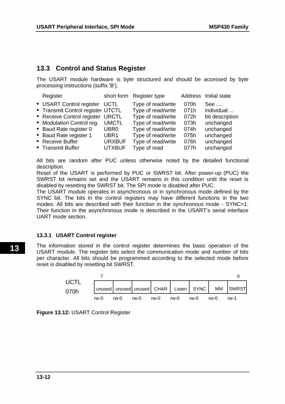
13.3 Control and Status Register
The USART module hardware is byte structured and should be accessed by byteprocessing instructions (suffix 'B').
Register short form Register type Address Initial state
• USART Control register UCTL Type of read/write 070h See ....• Transmit Control register UTCTL Type of read/write 071h individual ...• Receive Control register URCTL Type of read/write 072h bit description• Modulation Control reg. UMCTL Type of read/write 073h unchanged• Baud Rate register 0 UBR0 Type of read/write 074h unchanged• Baud Rate register 1 UBR1 Type of read/write 075h unchanged• Receive Buffer URXBUF Type of read/write 076h unchanged• Transmit Buffer UTXBUF Type of read 077h unchanged
All bits are random after PUC unless otherwise noted by the detailed functionaldescription.Reset of the USART is performed by PUC or SWRST bit. After power-up (PUC) theSWRST bit remains set and the USART remains in this condition until the reset isdisabled by resetting the SWRST bit. The SPI mode is disabled after PUC.The USART module operates in asynchronous or in synchronous mode defined by theSYNC bit. The bits in the control registers may have different functions in the twomodes. All bits are described with their function in the synchronous mode - SYNC=1.Their function in the asynchronous mode is described in the USART’s serial interfaceUART mode section.
13.3.1 USART Control register
The information stored in the control register determines the basic operation of theUSART module. The register bits select the communication mode and number of bitsper character. All bits should be programmed according to the selected mode beforereset is disabled by resetting bit SWRST.
UCTL
rw-0 rw-0 rw-0 rw-0 rw-0 rw-0 rw-0 rw-1070h
7 0
SWRSTMMSYNCListenCHARunused unused unused
Figure 13.12: USART Control Register
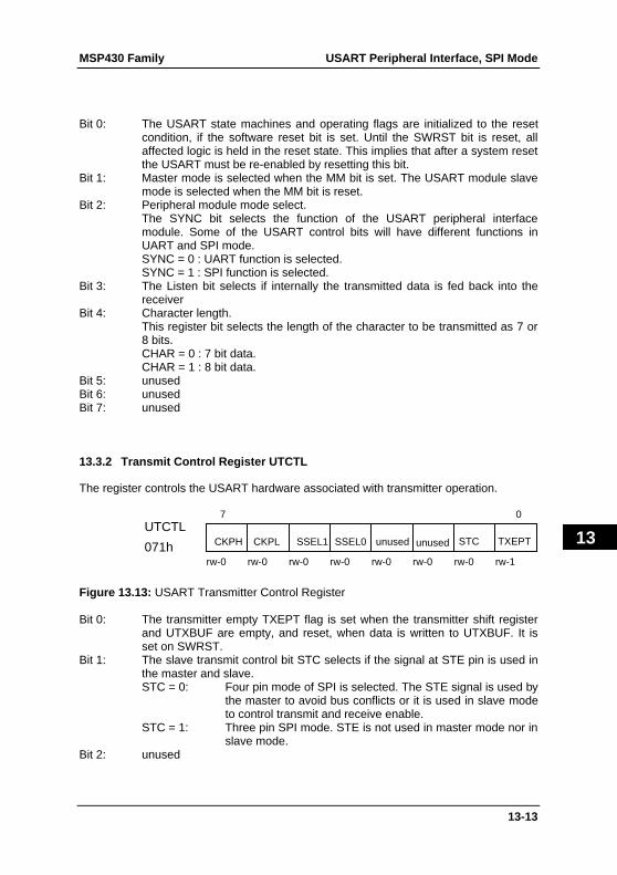
MSP430 Family USART Peripheral Interface, SPI Mode
13-13
13
Bit 0: The USART state machines and operating flags are initialized to the resetcondition, if the software reset bit is set. Until the SWRST bit is reset, allaffected logic is held in the reset state. This implies that after a system resetthe USART must be re-enabled by resetting this bit.
Bit 1: Master mode is selected when the MM bit is set. The USART module slavemode is selected when the MM bit is reset.
Bit 2: Peripheral module mode select.The SYNC bit selects the function of the USART peripheral interfacemodule. Some of the USART control bits will have different functions inUART and SPI mode.SYNC = 0 : UART function is selected.SYNC = 1 : SPI function is selected.
Bit 3: The Listen bit selects if internally the transmitted data is fed back into thereceiver
Bit 4: Character length.This register bit selects the length of the character to be transmitted as 7 or8 bits.CHAR = 0 : 7 bit data.CHAR = 1 : 8 bit data.
Bit 5: unusedBit 6: unusedBit 7: unused
13.3.2 Transmit Control Register UTCTL
The register controls the USART hardware associated with transmitter operation.
UTCTL
rw-0 rw-0 rw-0 rw-0 rw-0 rw-0 rw-0 rw-1071h
7 0
TXEPTSTCunusedSSEL1CKPL SSEL0CKPH unused
Figure 13.13: USART Transmitter Control Register
Bit 0: The transmitter empty TXEPT flag is set when the transmitter shift registerand UTXBUF are empty, and reset, when data is written to UTXBUF. It isset on SWRST.
Bit 1: The slave transmit control bit STC selects if the signal at STE pin is used inthe master and slave.STC = 0: Four pin mode of SPI is selected. The STE signal is used by
the master to avoid bus conflicts or it is used in slave modeto control transmit and receive enable.
STC = 1: Three pin SPI mode. STE is not used in master mode nor inslave mode.
Bit 2: unused
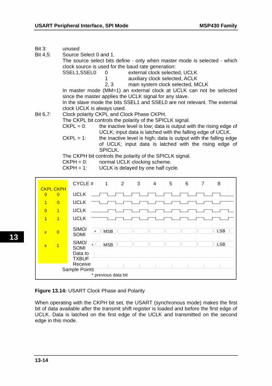
USART Peripheral Interface, SPI Mode MSP430 Family
13-14
13
Bit 3: unusedBit 4,5: Source Select 0 and 1.
The source select bits define - only when master mode is selected - whichclock source is used for the baud rate generation:SSEL1,SSEL0 0 external clock selected, UCLK
1 auxiliary clock selected, ACLK2, 3 main system clock selected, MCLK
In master mode (MM=1) an external clock at UCLK can not be selectedsince the master applies the UCLK signal for any slave.In the slave mode the bits SSEL1 and SSEL0 are not relevant. The externalclock UCLK is always used.
Bit 6,7: Clock polarity CKPL and Clock Phase CKPH.The CKPL bit controls the polarity of the SPICLK signal.CKPL = 0: the inactive level is low; data is output with the rising edge of
UCLK; input data is latched with the falling edge of UCLK.CKPL = 1: the inactive level is high; data is output with the falling edge
of UCLK; input data is latched with the rising edge ofSPICLK.
The CKPH bit controls the polarity of the SPICLK signal.CKPH = 0: normal UCLK clocking scheme.CKPH = 1: UCLK is delayed by one half cycle.
1 2 3 4 5 6 7 8CYCLE #
SIMO/
Sample Points
* MSB LSB
* previous data bit
SOMI
UCLK
UCLK
UCLK
UCLK
SIMO/ MSB LSBSOMI
TXBUFData to
*
Receive
CKPL CKPH 0 0
1 0
0 1
1 1
x 0
x 1
Figure 13.14: USART Clock Phase and Polarity
When operating with the CKPH bit set, the USART (synchronous mode) makes the firstbit of data available after the transmit shift register is loaded and before the first edge ofUCLK. Data is latched on the first edge of the UCLK and transmitted on the secondedge in this mode.
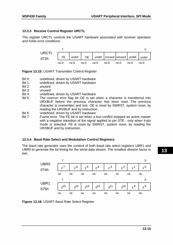
MSP430 Family USART Peripheral Interface, SPI Mode
13-15
13
13.3.3 Receive Control Register URCTL
The register URCTL controls the USART hardware associated with receiver operationand holds error conditions.
URCTL
rw-0 rw-0 rw-0 rw-0 rw-0 rw-0 rw-0 rw-0072h
7 0
OE unused unused undef.undef.undef.FE undef.
Figure 13.15: USART Transmitter Control Register
Bit 0: undefined, driven by USART hardwareBit 1: undefined, driven by USART hardwareBit 2: unusedBit 3: unusedBit 4: undefined, driven by USART hardwareBit 5: The overrun error flag bit OE is set when a character is transferred into
URXBUF before the previous character has been read. The previouscharacter is overwritten and lost. OE is reset by SWRST, system reset, byreading the URXBUF and by instruction.
Bit 6: undefined, driven by USART hardwareBit 7: Frame error. The FE bit is set when a bus conflict stopped an active master
with a negative transition of the signal applied to pin STE - only when 4-pinmode is selected. FE is reset by SWRST, system reset, by reading theURXBUF and by instruction.
13.3.4 Baud Rate Select and Modulation Control Registers
The baud rate generator uses the content of both baud rate select registers UBR1 andUBR0 to generate the bit timing for the serial data stream. The smallest division factor istwo.
UBR0
rw rw rw rw rw rw rw rw074h
7 0
2
UBR1
rw rw rw rw rw rw rw rw075h
7 0
7 2 6 2 5 2 4 2 3 2 2 2 1 2 0
215 214 213 212 211 210 2 9 2 8
Figure 13.16: USART Baud Rate Select Register
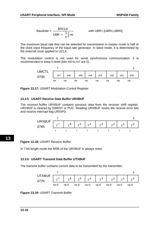
USART Peripheral Interface, SPI Mode MSP430 Family
13-16
13
Baudrate = BRCLK
UBR + 1n
mii
n
∑with UBR= [UBR1,UBR0]
The maximum baud rate that can be selected for transmission in master mode is half ofthe clock input frequency of the baud rate generator. In slave mode, it is determined bythe external clock applied to UCLK.
The modulation control is not used for serial synchronous communication. It isrecommended to keep it reset (bits m0 to m7 are 0).
UMCTL
rw rw rw rw rw rw rw rw073h
7 0
m7 m6 m4 m3 m2 m1 m0m5
Figure 13.17: USART Modulation Control Register
13.3.5 USART Receive Data Buffer URXBUF
The receiver buffer URXBUF contains previous data from the receiver shift register.URXBUF is cleared by SWRST or PUC. Reading URXBUF resets the receive error bitsand receive interrupt flag URXIFG.
URXBUF
r r r r r r r r076h
7 0
2 7 2 6 2 5 2 4 2 3 2 2 2 1 2 0
Figure 13.18: USART Receive Buffer
In 7-bit length mode the MSB of the URXBUF is always reset.
13.3.6 USART Transmit Data Buffer UTXBUF
The transmit buffer contains current data to be transmitted by the transmitter.
UTXBUF
rw-0 rw-0 rw-0 rw-0 rw-0 rw-0 rw-0 rw-0077h
7 0
2 7 2 6 2 5 2 4 2 3 2 2 2 1 2 0
Figure 13.19: USART Transmit Buffer
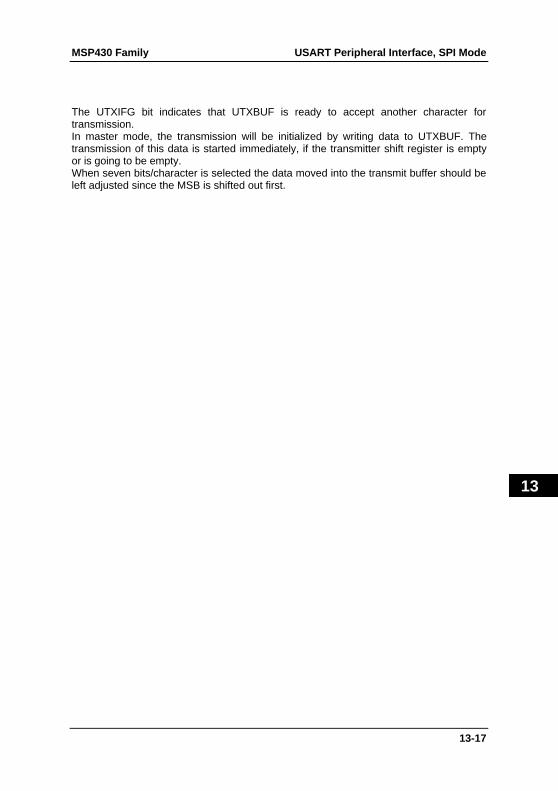
MSP430 Family USART Peripheral Interface, SPI Mode
13-17
13
The UTXIFG bit indicates that UTXBUF is ready to accept another character fortransmission.In master mode, the transmission will be initialized by writing data to UTXBUF. Thetransmission of this data is started immediately, if the transmitter shift register is emptyor is going to be empty.When seven bits/character is selected the data moved into the transmit buffer should beleft adjusted since the MSB is shifted out first.
USART Peripheral Interface, SPI Mode MSP430 Family
13-18
13