Embed Size (px)
Citation preview

EDC-UNITVIII Question&answer
GRIET-ECE G.Surekha Page 1
UNIT VIII-SPECIAL PURPOSE ELECTRONIC DEVICES
1. Explain tunnel Diode operation with the help of energy band diagrams.
TUNNEL DIODE:
A tunnel diode or Esaki diode is a type of semiconductor diode which is capable of very
fast operation, well into the microwave frequency region, by using quantum mechanical
effects. Impurity concentration in normal diode is 1 part in 810 in Tunnel diode 1 part in
310 .Normally a electron or hole must have energy greater than or equal to potential
energy barrier, to move to other side of the barrier. For very thin barrier there is a large
probability of electron penetrating through the barrier which is called as “Tunneling:.
Under normal Forward bias operation
As voltage begins to increase, electrons at first tunnel through the very narrow p–n junction
barrier because filled electron states in the conduction band on the n-side become aligned with
empty valence band hole states on the p-side of the p-n junction. As voltage increases further
these states become more misaligned and the current drops – this is called negative resistance
because current decreases with increasing voltage. As voltage increases yet further, the diode
begins to operate as a normal diode, where electrons travel by conduction across the p–n
junction, and no longer by tunneling through the p–n junction barrier. Thus the most important
operating region for a tunnel diode is the negative resistance region.
Reverse bias operation
When used in the reverse direction they are called back diodes and can act as fast rectifiers with
zero offset voltage and extreme linearity for power signals.Under reverse bias filled states on the
p-side become increasingly aligned with empty states on the n-side and electrons now tunnel
through the pn junction barrier in reverse direction.
ENERGY BAND STRUCTURE OF HIGHLY DOPED PN DIODE:
www.jntuworld.com
www.jntuworld.com

EDC-UNITVIII Question&answer
GRIET-ECE G.Surekha Page 2
ln CF C
D
NE E KT
N for N type material If NC < ND, EF > EC
Similarly for P type EF = EV+KT Cn
A
Nl
N If NA > NC; EF < EV
Fermi level lies in conduction band in N type as shown in Fig.5.23 (a).
Fermi level lies in valence band in P type material. Fermi level is at same energy level
on both sides. By reverse bailing barrier height increases as shown in fig.5.23 (b).Fermi
level on N side is lowered. Tunneling of electron from P to N side is the result. (From
filled sates to empty states). If we increase the reverse bias, reverse current increases as
shown in characteristics of (Fig.5.25) a.
www.jntuworld.com
www.jntuworld.com

EDC-UNITVIII Question&answer
GRIET-ECE G.Surekha Page 3
Similarly for forward bias tunneling occurs from N to P type material as shown in
Fig.5.24. Further increase in forward, the condition shown in 5.24(b)reached and
maximum current follows (characteristics of Fig.5.25).
Further increase will reduce the current as shown in fig.5.24(1) till a minimum current
flows due to the condition shown in fig.5.24(d) section 3 of 5.25(a)
Besides the above current due to tunneling normal diode current flows as shown in
dotted lives in fig.5.25(a). Resultant is the graph shown in 5.25(b).
The symbol and equivalent circuit is shown in the above fig5.26.
Application: -
1. Used as oscillator at VHF / UHF.
2. Ultra high speed switch.
3. Used as logic memory (storage) device.
4. Used as amplifier.
Advantages Disadvantages
1) Low noise 1) Less voltage range of separation
2) Ease of operation 2) No isolation of input and output,
3) High speed as it is a two terminal device.
4) Low power.
2. Differences between Tunnel Diode and PN Diode.
Impurity concentration in normal diode 1 part in 810
Impurity concentration in Tunnel diode 1 part in 310
Width of the junction barrio varies inversely as square root of impurity concentration
www.jntuworld.com
www.jntuworld.com

EDC-UNITVIII Question&answer
GRIET-ECE G.Surekha Page 4
2 2B
A
VW
e
Where VB is barrier potential, is the permitivity of material NA acceptor concentration.
Width of junction for normal diode 5 microns 65 10 m
Width of junction Tunnel Diode < 100 A0 10
-8m
Normally a electron or hole must have energy greater than or equal to potential energy
barrier, to move to other side of the barrier.
For very thin barrier there is a large probability of electron pert rating through the barrier
which is called as “Tunneling:. 3. Explain the principle and operation of varactor Diode.
Varactor or varicap diodes are used mainly in radio frequency (RF) circuits to be able to
provide a capacitance that can be varied by changing a voltage in an electronics circuit.
This can be used for tuning circuits including radio frequency oscillators and filters.
Although both names: varactor and varicap diode are used, they are both the same form
of diode. The name varactor meaning variable reactor, or reactance, and varicap meaning
variable capacitance (vari-cap).
Operation of a variable capacitor
They key to understanding how a varactor or varicap diode works is to look at what a
capacitor is and what can change the capacitance. As can be seen from the diagram
below, a capacitor consists of two plates with an insulating dielectric between them.
... the capacitance and the
amount of charge that can be
stored depends on the area of the
plates and the distance between
them....
The capacitance of the capacitor is dependent upon the area of the plates - the larger the
area the greater the capacitance, and also the distance between them - the greater the
distance the smaller the level of capacitance.
www.jntuworld.com
www.jntuworld.com

EDC-UNITVIII Question&answer
GRIET-ECE G.Surekha Page 5
A reverse biased diode has no current flowing between the P-type area and the N-type
area. The N-type region and the P-type regions can conduct electricity, and can be
considered to be the two plates, and the region between them - the depletion region is the
insulating dielectric. This is exactly the same as the capacitor above.
As with any diode, if the reverse bias is changed so does the size of the depletion region.
If the reverse voltage on the varactor or varicap diode is increased, the depletion region of
the diode increases and if the reverse voltage on varactor diode is decreased the depletion
region narrows. Therefore by changing the reverse bias on the diode it is possible to
change the capacitance.
Change of varactor diode capacitance with reverse bias
Varactor or varicap circuit symbol
The varactor diode or varicap diode is shown in circuit diagrams or schematics using a
symbol that combines the diode and capacitor symbols. In this way it is obvious that it is
being used as a varacor or varicap capacitor rather than a rectifying diode.
Circuit symbol for a varactor diode / varicap diode
When operated in a circuit, it is necessary to ensure the varactor diode remains reverse
biased. This means that the cathode will be positive with respect to the anode, i.e. the
cathode of the varactor will be more positive than the anode. Varactor Diode or
Varactors are operated reverse biased so no current flows, but since the thickness of the
depletion region varies with the applied bias voltage, the capacitance of the diode can be
made to vary. Generally, the depletion region thickness is proportional to the square root
of the applied voltage; and capacitance is inversely proportional to the depletion region
thickness.
www.jntuworld.com
www.jntuworld.com

EDC-UNITVIII Question&answer
GRIET-ECE G.Surekha Page 6
Applications:
They are used in PLL, voltage controlled oscillators, harmonic generation, electronic
tuning devices in tuners for television, mobiles, parametric amplification, AM radios,
voltage-variable tuning, frequency multipliers, etc.
4. Describe the working principle of an SCR with V-I characteristics and also explain two
transistor analogy of an SCR.
SILICON CONTROLLED RECTIFIER:
Construction of SCR
An SCR consists of four layers of alternating P and N type semiconductor materials. Silicon is
used as the intrinsic semiconductor, to which the proper dopants are added. The junctions are
either diffused or alloyed. The planar construction is used for low power SCRs (and all the
junctions are diffused). The mesa type construction is used for high power SCRs. In this case,
junction J2 is obtained by the diffusion method and then the outer two layers are alloyed to it,
since the PNPN pellet is required to handle large currents.
Construction Symbol
www.jntuworld.com
www.jntuworld.com

EDC-UNITVIII Question&answer
GRIET-ECE G.Surekha Page 7
CHARACTERISTICS OF SCR.
1) SCR is a three terminal four layer semiconductor device.
2) Leakage current is very small for SCR compared with germanium.
3) SCR acts as a switch when it is forward biased.
4) When gate is open i.e., IG = 0, and anode voltage is applied junctions P1 – N1 and P2 – N2 are
forward biased where N1 – P2 is reverse biased. Only small reverse current flows.
5) If we increase anode voltage further, at one stage anode current increases suddenly and
voltage across the SCR falls to holding voltage VH.
6) Once SCR fires (conducts), it will remain in conduction till the current through the device is
reduced less than IH, adding current by reducing applied voltage (to less than holding
voltage) close to zero.
7) The firing angle can be varied by varying the Gate voltage. With very large positive (gate
current break over may occur at very low voltage and SCR works as if it is a normal PN
diode.
TWO TRANSISTOR VERSION OF SCR.
-T1 is PNP and T2 is NPN.
www.jntuworld.com
www.jntuworld.com

EDC-UNITVIII Question&answer
GRIET-ECE G.Surekha Page 8
Ib1 = IA – Ie1 = IA - 1 IA = IA(1 - 1) - (1)
Ib1 = Ic2 and Ic2 = 2Ik - (2)
Ib1 = IA(1 - 1) = 2IK - (3)
We know Ik = IA + Ig. ( IA = IC1 + Ib1) - (4)
Putting the value of Ik from eqn. (4) in eqn. (3)
IA(1 - 1) - 2(IA + Ig)
IA(1 - 1) = 2(IA + Ig)
IA(1 - 1 - 2) = 2 Ig. Or 2
1 21
g
A
II -(5)
Equation 5 indicates that if( 1 + 2) = 1, IA =
- SCR is also called as Thyrister
- Latching current (IL) the min. current required to fire the device
- Holding current (IH) – min. current to keep the SCR conductivity
- Voltage safety factor 2 .
f
PIVV
RMS of operating voltage
Value of Vf is 2 to 2.7.
Application of SCRs
1. SCRs are mainly used in devices where the control of high power, possibly coupled with
high voltage, is demanded.
2. Their operation makes them suitable for use in medium to high-voltage AC power control
applications, such as regulators and motor control.
3. SCRs and similar devices are used for rectification of high power AC in high-voltage
direct current power transmission.
5. Explain Rectifier circuits using SCR’s.
SCR Half wave Rectifier:- Below fig shows the circuit of an SCR half wave rectifier.
www.jntuworld.com
www.jntuworld.com

EDC-UNITVIII Question&answer
GRIET-ECE G.Surekha Page 9
SCR does not conduct during negative half cycle (like normal PN diode)
Firing angle depends on gate voltage
Conduction angle is ( - )
During the positive half cycle of ac voltage appearing across secondary, the SCR will conduct
provided proper gate current, the lesser the supply voltage at which the SCR is triggered ON.
Reffering to above fig the gate current is adjusted to such a value that SCR is turned ON at a
positive voltage V1of ac secondary voltage which is less than the peak voltage Vm. Beyond this
The SCR will be conducting till the applied voltage becomes zero. The angle at which the SCR
starts conducting during the positive half cycle is called firing angle . There fore the conduction
angle is (1800- ).
Average DC output
0
1sin .
2av mV V wt dwt
0
1cos
2
1cos cos
2
11 cos
2
1 cos2
m
m
m
m
V wt
V
V
V
www.jntuworld.com
www.jntuworld.com

EDC-UNITVIII Question&answer
GRIET-ECE G.Surekha Page 10
RMS VOLTAGE: VRMS is given by
1/21
sin 22
m
RMS
VV
SCR FULL WAVE RECTIFIER
The SCR Full wave Rectifier is shown in below fig. During the Positive half cycle of the input
signal, anode of the SCR1 becomes positive and the at the same time the anode of SCR2
becomes negative. When the input voltage reaches V1 as shown in below fig (b), SCR1 starts
conducting and therefore only the shaded portion of positive half cycle will pass through the
load. During the negative half cycle of the input, the anode of SCR1 becomes negative and the
anode of SCR2 becomes positive. Hence SCR1 does not conduct and SCR2 conducts when the
input voltage becomes V1.
1 cosDC
VmV
6. Explain the principle and working of Photo Diode.
PHOTO DIODES: The diagrams shown below are construction, biasing and symbol of Photo
diode.
Construction Biasing Symbol
A P N K P N
www.jntuworld.com
www.jntuworld.com
EDC-UNITVIII Question&answer
GRIET-ECE G.Surekha Page 11
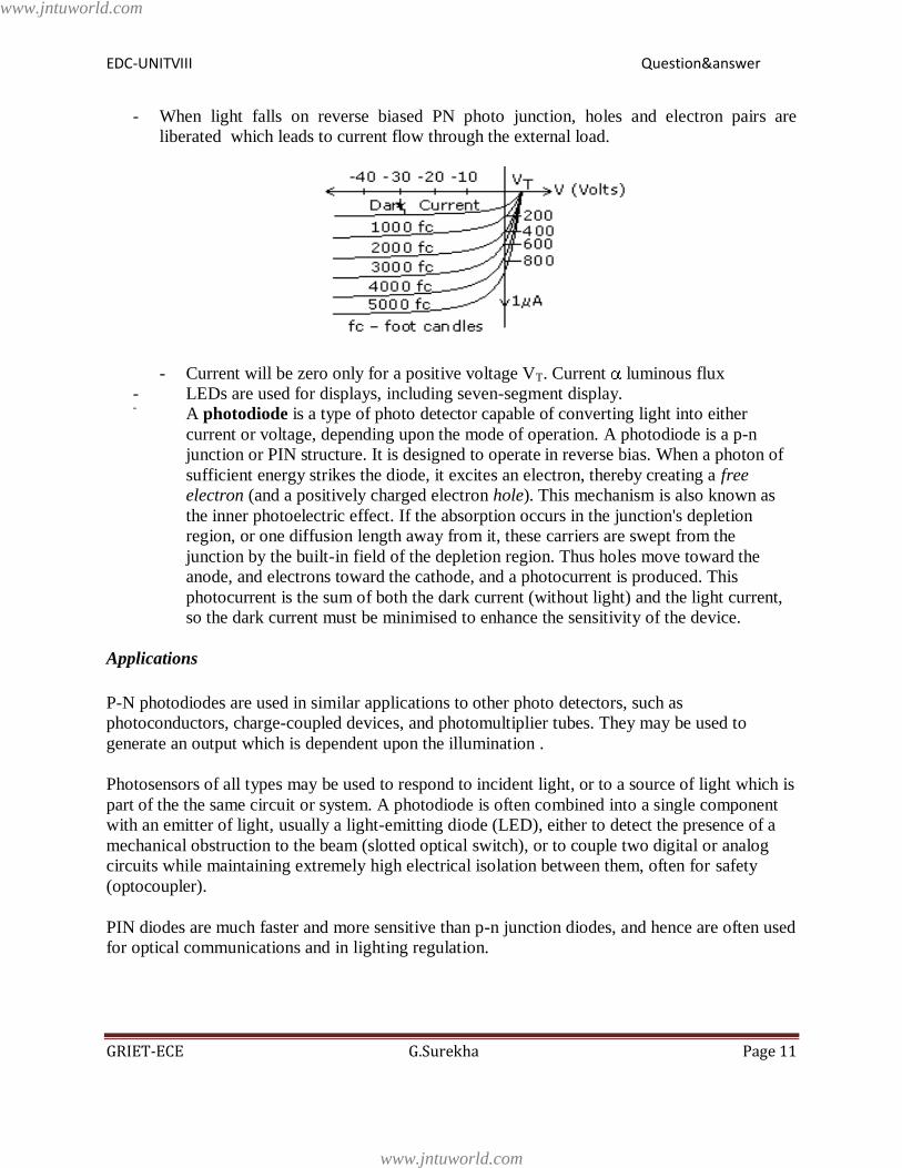
- When light falls on reverse biased PN photo junction, holes and electron pairs are
liberated which leads to current flow through the external load.
- Current will be zero only for a positive voltage VT. Current luminous flux
- LEDs are used for displays, including seven-segment display. - A photodiode is a type of photo detector capable of converting light into either
current or voltage, depending upon the mode of operation. A photodiode is a p-n
junction or PIN structure. It is designed to operate in reverse bias. When a photon of
sufficient energy strikes the diode, it excites an electron, thereby creating a free
electron (and a positively charged electron hole). This mechanism is also known as
the inner photoelectric effect. If the absorption occurs in the junction's depletion
region, or one diffusion length away from it, these carriers are swept from the
junction by the built-in field of the depletion region. Thus holes move toward the
anode, and electrons toward the cathode, and a photocurrent is produced. This
photocurrent is the sum of both the dark current (without light) and the light current,
so the dark current must be minimised to enhance the sensitivity of the device.
Applications
P-N photodiodes are used in similar applications to other photo detectors, such as
photoconductors, charge-coupled devices, and photomultiplier tubes. They may be used to
generate an output which is dependent upon the illumination .
Photosensors of all types may be used to respond to incident light, or to a source of light which is
part of the the same circuit or system. A photodiode is often combined into a single component
with an emitter of light, usually a light-emitting diode (LED), either to detect the presence of a
mechanical obstruction to the beam (slotted optical switch), or to couple two digital or analog
circuits while maintaining extremely high electrical isolation between them, often for safety
(optocoupler).
PIN diodes are much faster and more sensitive than p-n junction diodes, and hence are often used
for optical communications and in lighting regulation.
www.jntuworld.com
www.jntuworld.com

EDC-UNITVIII Question&answer
GRIET-ECE G.Surekha Page 12
7. Describe the operation of Schottky diode.
Schottky Diode
Junction of lightly doped n-type
semiconductor with a metal electrode.
The junction of a doped semiconductor (usually n-type)
with a metal electrode can produce a very fast-switching
diode which is mainly used in high frequency circuits or
high speed digital circuits. Under forward bias, the
electrons move from the n-type material to the metal
and give up their energy quickly. There are no holes
(minority carriers), so the conduction quickly stops
upon change to reverse bias. Schottky diodes find
application as rectifiers for high frequency signals.
Construction
A metal-semiconductor junction is formed between a metal and a semiconductor, creating a
Schottky barrier (instead of a semiconductor–semiconductor junction as in conventional diodes).
Typical metals used are molybdenum, platinum, chromium or tungsten; and the semiconductor
would typically be N-type silicon.The metal sides acts as the anode and N-type semiconductor
acts as the cathode of the diode. This Schottky barrier results in both very fast switching and low
forward voltage drop.
Reverse recovery time
The most important difference between p-n and Schottky diode is reverse recovery time, when
the diode switches from non-conducting to conducting state and vice versa. Where in a p-n diode
the reverse recovery time can be in the order of hundreds of nanoseconds and less than 100 ns for
fast diodes, Schottky diodes do not have a recovery time, as there is nothing to recover from (i.e.
no charge carrier depletion region at the junction). The switching time is ~100 ps for the small
signal diodes, and up to tens of nanoseconds for special high-capacity power diodes. It is often
said that the Schottky diode is a "majority carrier" semiconductor device. This means that if the
semiconductor body is doped n-type, only the n-type carriers (mobile electrons) play a
significant role in normal operation of the device. The majority carriers are quickly injected into
the conduction band of the metal contact on the other side of the diode to become free moving
electrons. Therefore no slow, random recombination of n- and p- type carriers is involved, so that
this diode can cease conduction faster than an ordinary p-n rectifier diode. This property in turn
allows a smaller device area, which also makes for a faster transition. This is another reason why
Schottky diodes are useful in switch-mode power converters; the high speed of the diode means
that the circuit can operate at frequencies in the range 200 kHz to 2 MHz, allowing the use of
small inductors and capacitors with greater efficiency than would be possible with other diode
types. Small-area Schottky diodes are the heart of RF detectors and mixers, which often operate
up to 50 GHz.
www.jntuworld.com
www.jntuworld.com

EDC-UNITVIII Question&answer
GRIET-ECE G.Surekha Page 13
Limitations
The most evident limitations of Schottky diodes are the relatively low reverse voltage rating for
silicon-metal Schottky diodes, 50 V and below, and a relatively high reverse leakage current.
Diode designs have been improving over time. Voltage ratings now can reach 200 V. Reverse
leakage current, because it increases with temperature, leads to a thermal instability.
Problems
Q)1. An SCR FWR is connected to 250V. 50 Hz mains to supply ac voltage to resistive load of
10 for firing angle of 90 . Find DC output voltage and load current.
Solution: -
Given VRMS = 230V, RL = 10 , = 90
VDC = ? IL = ?
max
2
1
RMS
mDC
VV
VV Cos
Or Vmax = VRMS 2 = 250 2 = 353.6 volts
353.61 cos90 112.6
112.611.26
10
DC
L
L
volts
VI Amps
R
Q 2) A sinusoidal voltage V = 200 sin 314 t is applied to an SCR whose forward break down
voltage is 150V. Determine the time during which SCR remain off.
Solution: -
Given V1 = 150V, Vm = 200V W = 314 = ? t = ?
1 sinmV V or 1 150 3sin
200 4m
V
V
1sin 3 / 4 48.6
T = 1/f f = ? w = 2 f = 314 or f = 314/2 = 50Hz.
www.jntuworld.com
www.jntuworld.com
EDC-UNITVIII Question&answer
GRIET-ECE G.Surekha Page 14
T= 1/50 = 0.02sec = 20 m. sec.
t = 48.6360 360
20 2.7 secT m
Q 3) A half wave rectifier employing SCR is adjusted to have a gate current of 1mA and its
forward breakdown voltage is 150V. If a sinusoidal voltage of 400V peak is applied, determine.
i) Firing angle (ii) Average output voltage
iii) Average current for a load resistance of 200
iv) Power output.
Given
V1 = 150V, Vm = 400V, = ? VDC = ? IDC = ? PDC = ? RL = 200
Solution: -
V1 = Vm sin , or Sin = V1 / Vm = 150/400 = 3/8 = 0.375.
= Sin-1
0.375 = 22 .
400 400
1 cos (1 cos 22 ) (1.927) 122.62 2 2
m
DC
VV volts
122.60.613 .
200
. 122.6 0.613 75.15 .
DCDC
L
DC DC DC
VI Amps
R
P V I Watts
www.jntuworld.com
www.jntuworld.com