Embed Size (px)
Citation preview
UNIT - 1
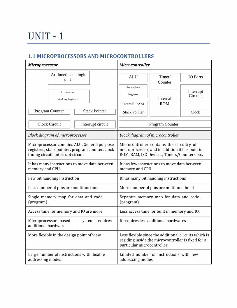
1.1 MICROPROCESSORS AND MICROCONTROLLERS
Microprocessor Microcontroller
Arithmetic and logic
ALU Timer/ IO Ports
unit
Counter
Accumulator
Interrupt
Accumulator Registers
Circuits
Working Registers Internal
Internal RAM ROM
Program Counter Stack Pointer Stack Pointer Clock
Clock Circuit Interrupt circuit Program Counter
Block diagram of microprocessor Block diagram of microcontroller
Microprocessor contains ALU, General purpose Microcontroller contains the circuitry of
registers, stack pointer, program counter, clock microprocessor, and in addition it has built in
timing circuit, interrupt circuit ROM, RAM, I/O Devices, Timers/Counters etc.
It has many instructions to move data between It has few instructions to move data between
memory and CPU memory and CPU
Few bit handling instruction It has many bit handling instructions
Less number of pins are multifunctional More number of pins are multifunctional
Single memory map for data and code Separate memory map for data and code
(program) (program)
Access time for memory and IO are more Less access time for built in memory and IO.
Microprocessor based system requires It requires less additional hardwares
additional hardware
More flexible in the design point of view Less flexible since the additional circuits which is
residing inside the microcontroller is fixed for a
particular microcontroller
Large number of instructions with flexible Limited number of instructions with few
addressing modes addressing modes
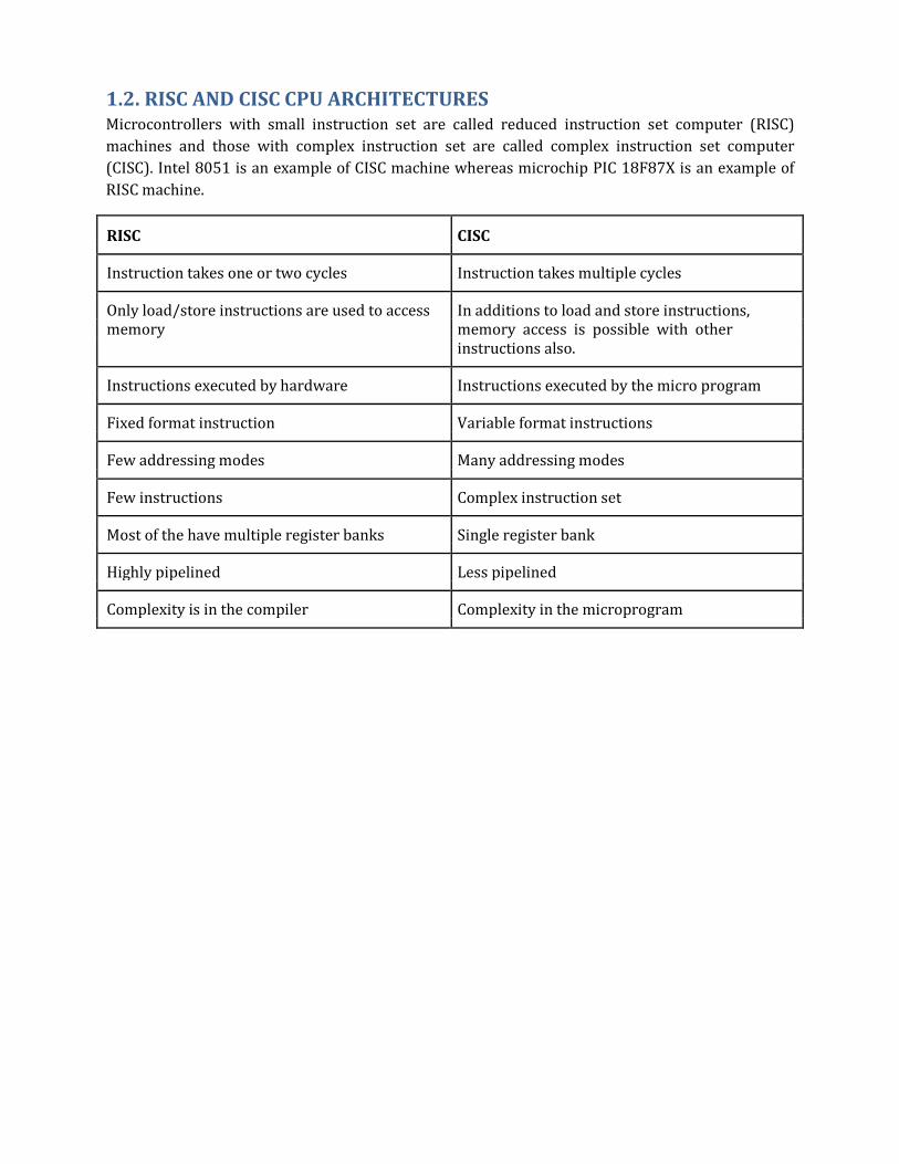
1.2. RISC AND CISC CPU ARCHITECTURES Microcontrollers with small instruction set are called reduced instruction set computer (RISC) machines and those with complex instruction set are called complex instruction set computer (CISC). Intel 8051 is an example of CISC machine whereas microchip PIC 18F87X is an example of RISC machine.
RISC CISC
Instruction takes one or two cycles Instruction takes multiple cycles
Only load/store instructions are used to access In additions to load and store instructions, memory memory access is possible with other
instructions also.
Instructions executed by hardware Instructions executed by the micro program
Fixed format instruction Variable format instructions
Few addressing modes Many addressing modes
Few instructions Complex instruction set
Most of the have multiple register banks Single register bank
Highly pipelined Less pipelined
Complexity is in the compiler Complexity in the microprogram
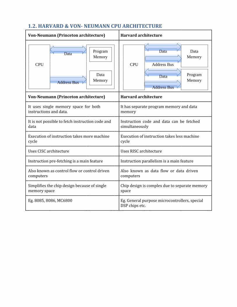
1.2. HARVARD & VON- NEUMANN CPU ARCHITECTURE
Von-Neumann (Princeton architecture) Harvard architecture
Data Data
Data Program
Memory Memory
CPU
CPU
Address Bus
Program
Data Data
Memory
Memory
Address Bus
Address Bus
Von-Neumann (Princeton architecture) Harvard architecture
It uses single memory space for both It has separate program memory and data
instructions and data. memory
It is not possible to fetch instruction code and Instruction code and data can be fetched
data simultaneously
Execution of instruction takes more machine Execution of instruction takes less machine
cycle cycle
Uses CISC architecture Uses RISC architecture
Instruction pre-fetching is a main feature Instruction parallelism is a main feature
Also known as control flow or control driven Also known as data flow or data driven
computers computers
Simplifies the chip design because of single Chip design is complex due to separate memory
memory space space
Eg. 8085, 8086, MC6800 Eg. General purpose microcontrollers, special
DSP chips etc.
1.3 COMPUTER SOFTWARE A set of instructions written in a specific sequence for the computer to solve a specific task is called a program and software is a collection of such programs. The program stored in the computer memory in the form of binary numbers is called machine instructions. The machine language program is called object code. An assembly language is a mnemonic representation of machine language. Machine language and assembly language are low level languages and are processor specific. The assembly language program the programmer enters is called source code. The source code (assembly language) is translated to object code (machine language) using assembler. Programs can be written in high level languages such as C, C++ etc. High level language will be converted to machine language using compiler or interpreter. Compiler reads the entire program and translate into the object code and then it is executed by the processor. Interpreter takes one statement of the high level language as input and translate it into object code and then executes. 1.4 THE 8051 ARCHITECTURE Introduction Salient features of 8051 microcontroller are given below.
• Eight bit CPU • On chip clock oscillator • 4Kbytes of internal program memory (code memory) [ROM] • 128 bytes of internal data memory [RAM] • 64 Kbytes of external program memory address space. • 64 Kbytes of external data memory address space. • 32 bi directional I/O lines (can be used as four 8 bit ports or 32 individually addressable I/O
lines) • Two 16 Bit Timer/Counter :T0, T1 • Full Duplex serial data receiver/transmitter • Four Register banks with 8 registers in each bank. • Sixteen bit Program counter (PC) and a data pointer (DPTR) • 8 Bit Program Status Word (PSW) • 8 Bit Stack Pointer • Five vector interrupt structure (RESET not considered as an interrupt.) • 8051 CPU consists of 8 bit ALU with associated registers like accumulator ‘A’ , B register,
PSW, SP, 16 bit program counter, stack pointer. • ALU can perform arithmetic and logic functions on 8 bit variables. • 8051 has 128 bytes of internal RAM which is divided into
o Working registers [00 – 1F] o Bit addressable memory area [20 – 2F] o General purpose memory area (Scratch pad memory) [30-7F]
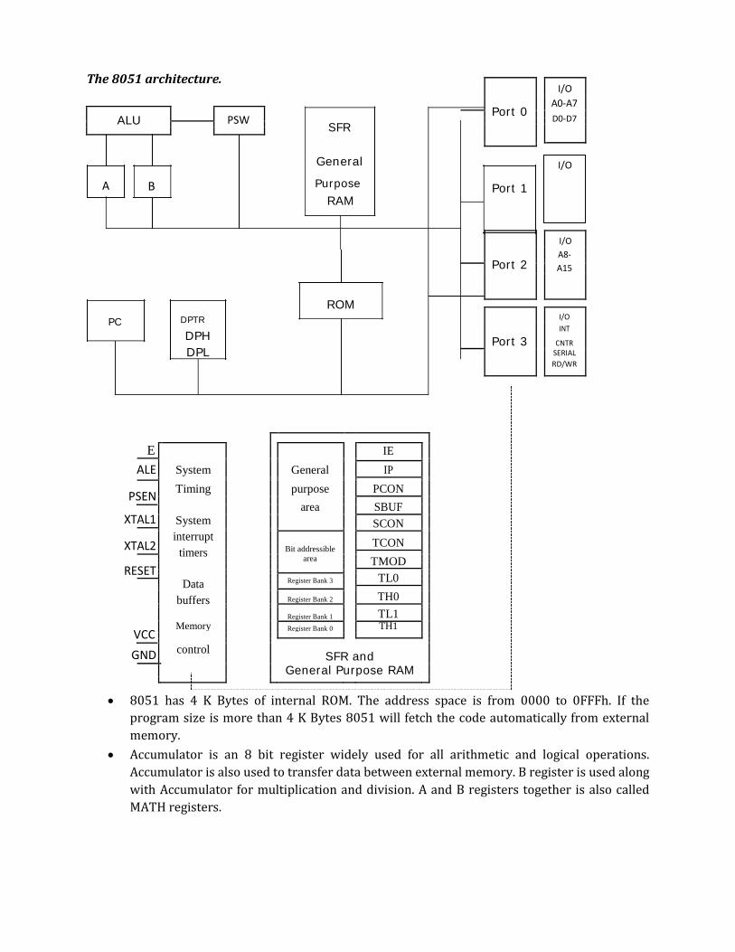
The 8051 architecture.
ALU PSW SFR
General
A B Purpose RAM
ROM PC DPTR
DPH DPL
E
IE
ALE System General IP
Timing
purpose
PCON
PSEN
System
area
SBUF
XTAL1
SCON
interrupt
XTAL2
Bit addressible TCON
timers
area TMOD
RESET
TL0
Data
Register Bank 3
TH0
Register Bank 2
buffers
Register Bank 1
TL1
VCC Memory Register Bank 0 TH1
control
SFR and
GND
General Purpose RAM
I/O
Port 0
A0-A7
D0-D7
I/O
Port 1
I/O
Port 2
A8-
A15
I/O
Port 3
INT
CNTR
SERIAL
RD/WR
• 8051 has 4 K Bytes of internal ROM. The address space is from 0000 to 0FFFh. If the
program size is more than 4 K Bytes 8051 will fetch the code automatically from external memory.
• Accumulator is an 8 bit register widely used for all arithmetic and logical operations. Accumulator is also used to transfer data between external memory. B register is used along with Accumulator for multiplication and division. A and B registers together is also called MATH registers.
• PSW (Program Status Word). This is an 8 bit register which contains the arithmetic status of ALU and the bank select bits of register banks. CY AC F0 RS1 RS0 OV - P CY - carry flag AC - auxiliary carry flag F0 - available to the user for general purpose RS1,RS0 - register bank select bits OV - overflow P - parity
• Stack Pointer (SP) – it contains the address of the data item on the top of the stack. Stack may reside anywhere on the internal RAM. On reset, SP is initialized to 07 so that the default stack will start from address 08 onwards.
• Data Pointer (DPTR) – DPH (Data pointer higher byte), DPL (Data pointer lower byte). This is a 16 bit register which is used to furnish address information for internal and external program memory and for external data memory.
• Program Counter (PC) – 16 bit PC contains the address of next instruction to be executed. On reset PC will set to 0000. After fetching every instruction PC will increment by one.
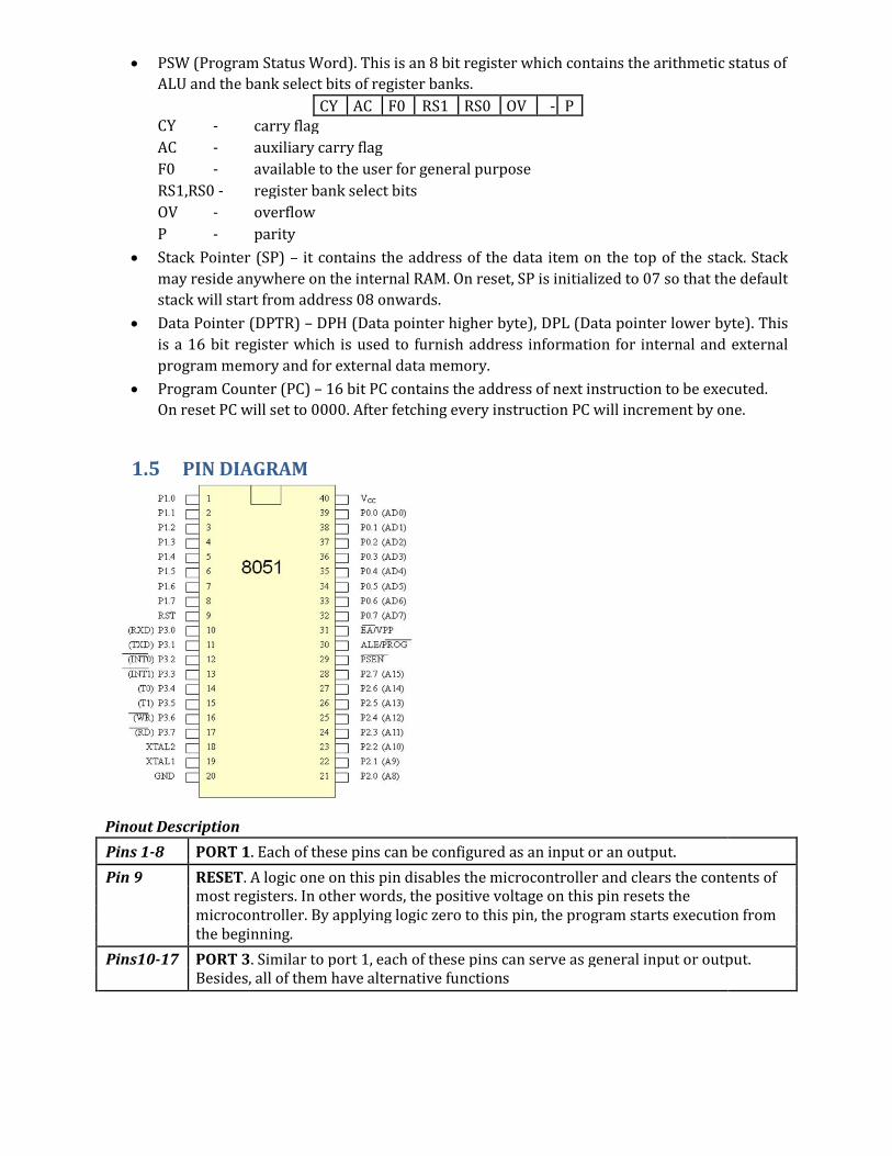
1.5 PIN DIAGRAM
Pinout Description Pins 1-8 PORT 1. Each of these pins can be configured as an input or an output.
Pin 9 RESET. A logic one on this pin disables the microcontroller and clears the contents of most registers. In other words, the positive voltage on this pin resets the microcontroller. By applying logic zero to this pin, the program starts execution from the beginning.
Pins10-17 PORT 3. Similar to port 1, each of these pins can serve as general input or output. Besides, all of them have alternative functions
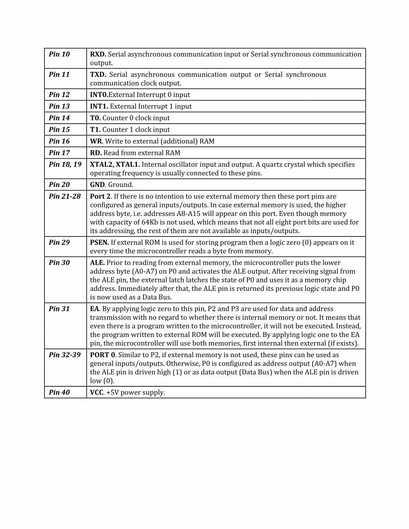
Pin 10 RXD. Serial asynchronous communication input or Serial synchronous communication
output.
Pin 11 TXD. Serial asynchronous communication output or Serial synchronous communication clock output.
Pin 12 INT0.External Interrupt 0 input
Pin 13 INT1. External Interrupt 1 input
Pin 14 T0. Counter 0 clock input
Pin 15 T1. Counter 1 clock input
Pin 16 WR. Write to external (additional) RAM
Pin 17 RD. Read from external RAM
Pin 18, 19 XTAL2, XTAL1. Internal oscillator input and output. A quartz crystal which specifies operating frequency is usually connected to these pins.
Pin 20 GND. Ground.
Pin 21-28 Port 2. If there is no intention to use external memory then these port pins are configured as general inputs/outputs. In case external memory is used, the higher address byte, i.e. addresses A8-A15 will appear on this port. Even though memory with capacity of 64Kb is not used, which means that not all eight port bits are used for its addressing, the rest of them are not available as inputs/outputs.
Pin 29 PSEN. If external ROM is used for storing program then a logic zero (0) appears on it every time the microcontroller reads a byte from memory.
Pin 30 ALE. Prior to reading from external memory, the microcontroller puts the lower address byte (A0-A7) on P0 and activates the ALE output. After receiving signal from the ALE pin, the external latch latches the state of P0 and uses it as a memory chip address. Immediately after that, the ALE pin is returned its previous logic state and P0 is now used as a Data Bus.
Pin 31 EA. By applying logic zero to this pin, P2 and P3 are used for data and address transmission with no regard to whether there is internal memory or not. It means that even there is a program written to the microcontroller, it will not be executed. Instead, the program written to external ROM will be executed. By applying logic one to the EA pin, the microcontroller will use both memories, first internal then external (if exists).
Pin 32-39 PORT 0. Similar to P2, if external memory is not used, these pins can be used as general inputs/outputs. Otherwise, P0 is configured as address output (A0-A7) when the ALE pin is driven high (1) or as data output (Data Bus) when the ALE pin is driven low (0).
Pin 40 VCC. +5V power supply.
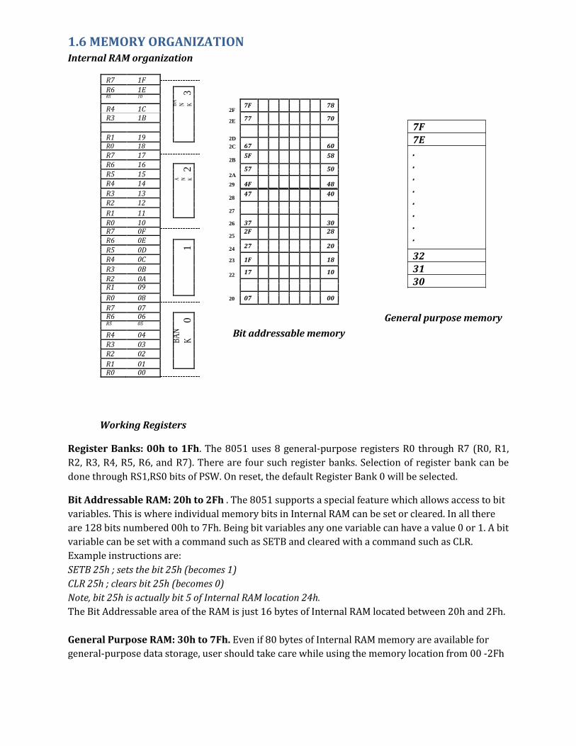
1.6 MEMORY ORGANIZATION Internal RAM organization
R7 1F
R6 1E
3
R5 1D
BA N K
7F 78
R4 1C 2F
6F 68 R2 1A
R3 1B 2E 77 70
R1 19 2D
67
60
R0 18 2C
R7 17 2B 5F 58
R6 16
2 57 50
R5 15
2A
A N K 4F
48
R4 14 29
3F 38
R3 13 28 47 40
R2 12
R1 11 27
37
30
R0 10 26
R7 0F 25 2F 28
R6 0E
27
20
R5 0D 1 24
R4 0C
23 1F 18
21 0F 08
R3 0B
22 17 10
R2 0A
R1 09
R0 08
20 07
00
R7 07
R6 06 0
R5 05
BAN
K
Bit addressable memory
R4 04
R3 03
R2 02
R1 01
R0 00
7F 7E . . . . . . . .
32 31 30
General purpose memory
Working Registers
Register Banks: 00h to 1Fh. The 8051 uses 8 general-purpose registers R0 through R7 (R0, R1, R2, R3, R4, R5, R6, and R7). There are four such register banks. Selection of register bank can be done through RS1,RS0 bits of PSW. On reset, the default Register Bank 0 will be selected. Bit Addressable RAM: 20h to 2Fh . The 8051 supports a special feature which allows access to bit variables. This is where individual memory bits in Internal RAM can be set or cleared. In all there are 128 bits numbered 00h to 7Fh. Being bit variables any one variable can have a value 0 or 1. A bit variable can be set with a command such as SETB and cleared with a command such as CLR. Example instructions are: SETB 25h ; sets the bit 25h (becomes 1) CLR 25h ; clears bit 25h (becomes 0) Note, bit 25h is actually bit 5 of Internal RAM location 24h. The Bit Addressable area of the RAM is just 16 bytes of Internal RAM located between 20h and 2Fh. General Purpose RAM: 30h to 7Fh. Even if 80 bytes of Internal RAM memory are available for general-purpose data storage, user should take care while using the memory location from 00 -2Fh
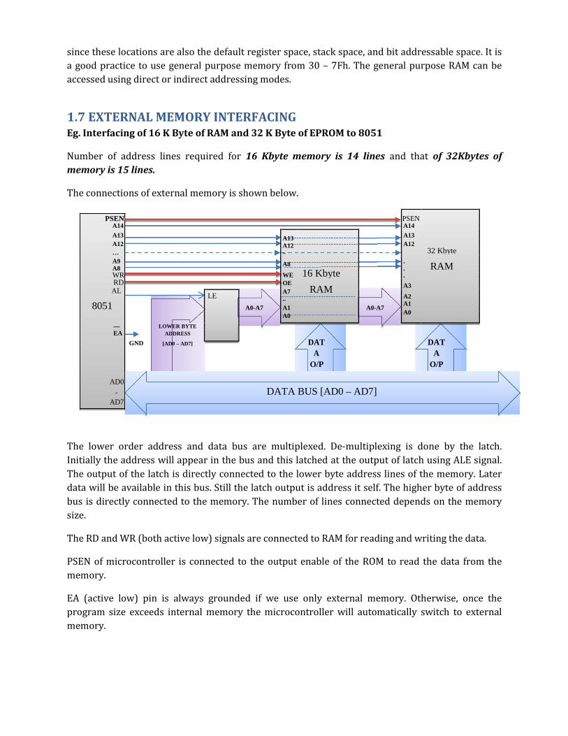
since these locations are also the default register space, stack space, and bit addressable space. It is a good practice to use general purpose memory from 30 – 7Fh. The general purpose RAM can be accessed using direct or indirect addressing modes. 1.7 EXTERNAL MEMORY INTERFACING Eg. Interfacing of 16 K Byte of RAM and 32 K Byte of EPROM to 8051 Number of address lines required for 16 Kbyte memory is 14 lines and that of 32Kbytes of memory is 15 lines. The connections of external memory is shown below.
PSEN PSEN
A14 A14
A13 A13 A13
A12
A12
A12
… 32 Kbyte
..
A9 A8 . RAM
A8 .
WE 16 Kbyte
WR .
RD OE RAM
A3
AL
A7
LE A2
..
8051
A0-A7
A0-A7 A1
A1
A0
A0
__ LOWER BYTE
EA ADDRESS
GND [AD0 – AD7]
DAT DAT
A A
O/P O/P
AD0
- DATA BUS [AD0 – AD7] AD7
The lower order address and data bus are multiplexed. De-multiplexing is done by the latch. Initially the address will appear in the bus and this latched at the output of latch using ALE signal. The output of the latch is directly connected to the lower byte address lines of the memory. Later data will be available in this bus. Still the latch output is address it self. The higher byte of address bus is directly connected to the memory. The number of lines connected depends on the memory size. The RD and WR (both active low) signals are connected to RAM for reading and writing the data. PSEN of microcontroller is connected to the output enable of the ROM to read the data from the memory. EA (active low) pin is always grounded if we use only external memory. Otherwise, once the program size exceeds internal memory the microcontroller will automatically switch to external memory.
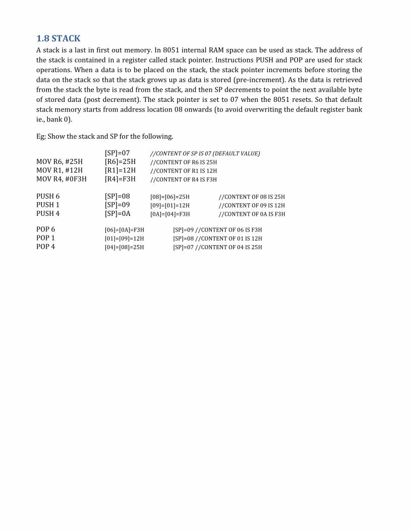
1.8 STACK A stack is a last in first out memory. In 8051 internal RAM space can be used as stack. The address of the stack is contained in a register called stack pointer. Instructions PUSH and POP are used for stack operations. When a data is to be placed on the stack, the stack pointer increments before storing the data on the stack so that the stack grows up as data is stored (pre-increment). As the data is retrieved from the stack the byte is read from the stack, and then SP decrements to point the next available byte of stored data (post decrement). The stack pointer is set to 07 when the 8051 resets. So that default stack memory starts from address location 08 onwards (to avoid overwriting the default register bank ie., bank 0). Eg; Show the stack and SP for the following. [SP]=07 //CONTENT OF SP IS 07 (DEFAULT VALUE) MOV R6, #25H [R6]=25H //CONTENT OF R6 IS 25H MOV R1, #12H [R1]=12H //CONTENT OF R1 IS 12H MOV R4, #0F3H [R4]=F3H //CONTENT OF R4 IS F3H
PUSH 6 [SP]=08 [08]=[06]=25H //CONTENT OF 08 IS 25H PUSH 1 [SP]=09 [09]=[01]=12H //CONTENT OF 09 IS 12H PUSH 4 [SP]=0A [0A]=[04]=F3H //CONTENT OF 0A IS F3H POP 6 [06]=[0A]=F3H [SP]=09 //CONTENT OF 06 IS F3H POP 1 [01]=[09]=12H [SP]=08 //CONTENT OF 01 IS 12H POP 4 [04]=[08]=25H [SP]=07 //CONTENT OF 04 IS 25H
UNIT 2
2.1 INSTRUCTION SYNTAX. General syntax for 8051 assembly language is as follows.
LABEL: OPCODE OPERAND ;COMMENT
LABEL : (THIS IS NOT NECESSARY UNLESS THAT SPECIFIC LINE HAS TO BE ADDRESSED). The label is a symbolic address for the instruction. When the program is assembled, the label will be given specific address in which that instruction is stored. Unless that specific line of instruction is needed by a branching instruction in the program, it is not necessary to label that line.
OPCODE: Opcode is the symbolic representation of the operation. The assembler converts the opcode to a unique binary code (machine language).
OPERAND: While opcode specifies what operation to perform, operand specifies where to perform that action. The operand field generally contains the source and destination of the data. In some cases only source or destination will be available instead of both. The operand will be either address of the data, or data itself.
COMMENT: Always comment will begin with ; or // symbol. To improve the program quality, programmer may always use comments in the program.
2.2 ADDRESSING MODES Various methods of accessing the data are called addressing modes.
8051 addressing modes are classified as follows.
1. Immediate addressing. 2. Register addressing. 3. Direct addressing. 4. Indirect addressing. 5. Relative addressing. 6. Absolute addressing. 7. Long addressing. 8. Indexed addressing. 9. Bit inherent addressing. 10. Bit direct addressing.
1. Immediate addressing. In this addressing mode the data is provided as a part of instruction itself. In other words
data immediately follows the instruction. Eg.
MOV A,#30H ADD A, #83
# Symbol indicates the data is immediate.
2. Register addressing. In this addressing mode the register will hold the data. One of the eight general registers (R0 to R7) can be used and specified as the operand. Eg. MOV A,R0 ADD A,R6 R0 – R7 will be selected from the current selection of register bank. The default register bank will be bank 0.
3. Direct addressing There are two ways to access the internal memory. Using direct address and indirect address. Using direct addressing mode we can not only address the internal memory but SFRs also. In direct addressing, an 8 bit internal data memory address is specified as part of the instruction and hence, it can specify the address only in the range of 00H to FFH. In this addressing mode, data is obtained directly from the memory. Eg. MOV A,60h ADD A,30h 4. Indirect addressing The indirect addressing mode uses a register to hold the actual address that will be used in data movement. Registers R0 and R1 and DPTR are the only registers that can be used as data pointers. Indirect addressing cannot be used to refer to SFR registers. Both R0 and R1 can hold 8 bit address and DPTR can hold 16 bit address. Eg. MOV A,@R0 ADD A,@R1 MOVX A,@DPTR
5. Indexed addressing. In indexed addressing, either the program counter (PC), or the data pointer (DTPR)—is used to hold the base address, and the A is used to hold the offset address. Adding the value of the base address to the value of the offset address forms the effective address. Indexed addressing is used with JMP or MOVC instructions. Look up tables are easily implemented with the help of index addressing. Eg. MOVC A, @A+DPTR // copies the contents of memory location pointed by the sum of the accumulator A and the DPTR into accumulator A. MOVC A, @A+PC // copies the contents of memory location pointed by the sum of the accumulator A and the program counter into accumulator A.
6. Relative Addressing. Relative addressing is used only with conditional jump instructions. The relative address, (offset), is an 8 bit signed number, which is automatically added to the PC to make the address of the next instruction. The 8 bit signed offset value gives an address range of +127 to —128 locations. The jump destination is usually specified using a label and the assembler calculates the jump offset accordingly. The advantage of relative addressing is that the program code is easy to relocate and the address is relative to position in the memory. Eg. SJMP LOOP1 JC BACK
7. Absolute addressing Absolute addressing is used only by the AJMP (Absolute Jump) and ACALL (Absolute Call)
instructions. These are 2 bytes instructions. The absolute addressing mode specifies the lowest 11 bit of the memory address as part of the instruction. The upper 5 bit of the destination address are
the upper 5 bit of the current program counter. Hence, absolute addressing allows branching only within the current 2 Kbyte page of the program memory. Eg.
AJMP LOOP1 ACALL LOOP2
8. Long Addressing The long addressing mode is used with the instructions LJMP and LCALL. These are 3 byte
instructions. The address specifies a full 16 bit destination address so that a jump or a call can be made to a location within a 64 Kbyte code memory space. Eg.
LJMP FINISH LCALL DELAY
9. Bit Inherent Addressing In this addressing, the address of the flag which contains the operand, is implied in the opcode
of the instruction. Eg. CLR C ; Clears the carry flag to 0 10. Bit Direct Addressing
In this addressing mode the direct address of the bit is specified in the instruction. The RAM space 20H to 2FH and most of the special function registers are bit addressable. Bit address values are between 00H to 7FH. Eg.
CLR 07h SETB 07H
; ;
Clears the bit 7 of 20h RAM space Sets the bit 7 of 20H RAM space.
2.3 INSTRUCTION SET. 1. Instruction Timings The 8051 internal operations and external read/write operations are controlled by the oscillator clock. T-state, Machine cycle and Instruction cycle are terms used in instruction timings. T-state is defined as one subdivision of the operation performed in one clock period. The terms 'T-state' and 'clock period' are often used synonymously. Machine cycle is defined as 12 oscillator periods. A machine cycle consists of six states and each state lasts for two oscillator periods. An instruction takes one to four machine cycles to execute an instruction. Instruction cycle is defined as the time required for completing the execution of an instruction. The 8051 instruction cycle consists of one to four machine cycles. Eg. If 8051 microcontroller is operated with 12 MHz oscillator, find the execution time for the following four instructions.
1. ADD A, 45H 2. SUBB A, #55H 3. MOV DPTR, #2000H 4. MUL AB
Since the oscillator frequency is 12 MHz, the clock period is, Clock period = 1/12 MHz = 0.08333 µS. Time for 1 machine cycle = 0.08333 µS x 12 =1 µS.
Instruction No. of machine cycles ADD A, 45H 1 1.
1 µs
Execution time
2. SUBB A, #55H 2 2 µs 3. MOV DPTR, #2000H 2 2 µs 4. MUL AB 4 4 µs
2. 8051 Instructions The instructions of 8051 can be broadly classified under the following headings.
1. Data transfer instructions 2. Arithmetic instructions 3. Logical instructions 4. Branch instructions 5. Subroutine instructions 6. Bit manipulation instructions
Data transfer instructions. In this group, the instructions perform data transfer operations of the following types.
a. Move the contents of a register Rn to A i. MOV A,R2
ii. MOV A,R7 b. Move the contents of a register A to Rn
i. MOV R4,A ii. MOV R1,A
c. Move an immediate 8 bit data to register A or to Rn or to a memory location(direct or indirect)
i. MOV A, #45H iv. MOV @R0, #0E8H ii. MOV R6, #51H v. MOV DPTR, #0F5A2H iii. MOV 30H, #44H vi. MOV DPTR, #5467H
d. Move the contents of a memory location to A or A to a memory location using direct and indirect addressing
i. MOV A, 65H ii. MOV A, @R0
iii. MOV 45H, A iv. MOV @R1, A
e. Move the contents of a memory location to Rn or Rn to a memory location using direct addressing
i. MOV R3, 65H ii. MOV 45H, R2
f. Move the contents of memory location to another memory location using direct and indirect addressing
i. MOV 47H, 65H ii. MOV 45H, @R0
g. Move the contents of an external memory to A or A to an external memory i. MOVX A,@R1
ii. MOVX @R0,A
iii. MOVX A,@DPTR iv. MOVX@DPTR,A
h. Move the contents of program memory to A i. MOVC A, @A+PC
ii. MOVC A, @A+DPTR
FIG. Addressing Using MOV, MOVX and MOVC
i. Push and Pop instructions
MOV R6, #25H MOV R1, #12H MOV R4, #0F3H
PUSH 6 PUSH 1 PUSH 4
POP 6 POP 1 POP 4
[SP]=07 //CONTENT OF SP IS 07 (DEFAULT VALUE) [R6]=25H //CONTENT OF R6 IS 25H [R1]=12H //CONTENT OF R1 IS 12H [R4]=F3H //CONTENT OF R4 IS F3H
[SP]=08 [08]=[06]=25H //CONTENT OF 08 IS 25H [SP]=09 [09]=[01]=12H //CONTENT OF 09 IS 12H [SP]=0A [0A]=[04]=F3H //CONTENT OF 0A IS F3H
[06]=[0A]=F3H [SP]=09 //CONTENT OF 06 IS F3H [01]=[09]=12H [SP]=08 //CONTENT OF 01 IS 12H [04]=[08]=25H [SP]=07 //CONTENT OF 04 IS 25H
j. Exchange instructions The content of source ie., register, direct memory or indirect memory will be exchanged with the contents of destination ie., accumulator.
i. XCH A,R3 ii. XCH A,@R1
iii. XCH A,54h k. Exchange digit. Exchange the lower order nibble of Accumulator (A0-A3) with lower
order nibble of the internal RAM location which is indirectly addressed by the register. i. XCHD A,@R1
ii. XCHD A,@R0
Arithmetic instructions. The 8051 can perform addition, subtraction. Multiplication and division operations on 8 bit numbers. Addition In this group, we have instructions to
i. Add the contents of A with immediate data with or without carry. i. ADD A, #45H
ii. ADDC A, #OB4H ii. Add the contents of A with register Rn with or without carry.
i. ADD A, R5 ii. ADDC A, R2
iii. Add the contents of A with contents of memory with or without carry using direct and indirect addressing i. ADD A, 51H
ii. ADDC A, 75H iii. ADD A, @R1 iv. ADDC A, @R0
CY AC and OV flags will be affected by this operation. Subtraction In this group, we have instructions to
i. Subtract the contents of A with immediate data with or without carry. i. SUBB A, #45H
ii. SUBB A, #OB4H ii. Subtract the contents of A with register Rn with or without carry.
i. SUBB A, R5 ii. SUBB A, R2
iii. Subtract the contents of A with contents of memory with or without carry using direct and indirect addressing i. SUBB A, 51H
ii. SUBB A, 75H iii. SUBB A, @R1 iv. SUBB A, @R0
CY AC and OV flags will be affected by this operation. Multiplication MUL AB. This instruction multiplies two 8 bit unsigned numbers which are stored in A and B register. After multiplication the lower byte of the result will be stored in accumulator and higher byte of result will be stored in B register. Eg.
MOV A,#45H MOV B,#0F5H MUL AB
;[A]=45H ;[B]=F5H ;[A] x [B] = 45 x F5 = 4209 ;[A]=09H, [B]=42H
Division
DIV AB. This instruction divides the 8 bit unsigned number which is stored in A by the 8 bit unsigned number which is stored in B register. After division the result will be stored in accumulator and remainder will be stored in B register. Eg.
MOV A,#45H MOV B,#0F5H DIV AB
;[A]=0E8H ;[B]=1BH ;[A] / [B] = E8 /1B = 08 H with remainder
10H
;[A] = 08H, [B]=10H DA A (Decimal Adjust After Addition).
When two BCD numbers are added, the answer is a non-BCD number. To get the result in BCD, we use DA A instruction after the addition. DA A works as follows.
• If lower nibble is greater than 9 or auxiliary carry is 1, 6 is added to lower nibble. • If upper nibble is greater than 9 or carry is 1, 6 is added to upper nibble.
Eg 1: MOV A,#23H
MOV R1,#55H ADD A,R1 DA A
// [A]=78 // [A]=78
no changes in the accumulator after da a
Eg 2: MOV A,#53H MOV R1,#58H ADD A,R1
// [A]=ABh
DA A // [A]=11, C=1 . ANSWER IS 111.
Accumulator data is changed after DA A
Increment: increments the operand by one.
INC A
INC Rn
INC DIRECT
INC @Ri INC DPTR
INC increments the value of source by 1. If the initial value of register is FFh, incrementing the value will cause it to reset to 0. The Carry Flag is not set when the value "rolls over" from 255 to 0.
In the case of "INC DPTR", the value two-byte unsigned integer value of DPTR is incremented. If the initial value of DPTR is FFFFh, incrementing the value will cause it to reset to 0.
Decrement: decrements the operand by one.
DEC A DEC Rn DEC DIRECT DEC @Ri
DEC decrements the value of source by 1. If the initial value of is 0, decrementing the value will cause it to reset to FFh. The Carry Flag is not set when the value "rolls over" from 0 to FFh.
Logical Instructions Logical AND
ANL destination, source: ANL does a bitwise "AND" operation between source and destination, leaving the resulting value in destination. The value in source is not affected. "AND" instruction logically AND the bits of source and destination. ANL A,#DATA ANL A, Rn ANL A,DIRECT ANL A,@Ri ANL DIRECT,A ANL DIRECT, #DATA
Logical OR
ORL
destination, source:
ORL does a bitwise "OR" operation between source and destination,
leaving the resulting value in destination. The value in source is not affected. " OR " instruction logically OR the bits of source and destination. ORL A,#DATA ORL A, Rn ORL A,DIRECT ORL A,@Ri ORL DIRECT,A ORL DIRECT, #DATA
Logical Ex-OR
XRL destination, source: XRL does a bitwise "EX-OR" operation between source and destination, leaving the resulting value in destination. The value in source is not affected. " XRL " instruction logically EX-OR the bits of source and destination. XRL A,#DATA XRL A,Rn XRL A,DIRECT XRL A,@Ri XRL DIRECT,A XRL DIRECT, #DATA
Logical NOT
CPL complements operand, leaving the result in operand. If operand is a single bit then the state of the bit will be reversed. If operand is the Accumulator then all the bits in the Accumulator will be reversed.
CPL A, CPL C, CPL bit address
SWAP A – Swap the upper nibble and lower nibble of A.
Rotate Instructions RR A This instruction is rotate right the accumulator. Its operation is illustrated below. Each bit is shifted one location to the right, with bit 0 going to bit 7. RL A Rotate left the accumulator. Each bit is shifted one location to the left, with bit 7 going to bit 0 RRC A Rotate right through the carry. Each bit is shifted one location to the right, with bit 0 going into the carry bit in the PSW, while the carry was at goes into bit 7 RLC A Rotate left through the carry. Each bit is shifted one location to the left, with bit 7 going into the carry bit in the PSW, while the carry goes into bit 0.
Branch (JUMP) Instructions Jump and Call Program Range There are 3 types of jump instructions. They are:-
1. Relative Jump 2. Short Absolute Jump 3. Long Absolute Jump
Relative Jump Jump that replaces the PC (program counter) content with a new address that is greater than (the address following the jump instruction by 127 or less) or less than (the address following the jump by 128 or less) is called a relative jump. Schematically, the relative jump can be shown as follows: - The advantages of the relative jump are as follows:-
1. Only 1 byte of jump address needs to be specified in the 2's complement form, ie. For jumping ahead, the range is 0 to 127 and for jumping back, the range is -1 to -128.
2. Specifying only one byte reduces the size of the instruction and speeds up program execution.
3. The program with relative jumps can be relocated without reassembling to generate absolute jump addresses.
Disadvantages of the absolute jump: -
1. Short jump range (-128 to 127 from the instruction following the jump
instruction) Instructions that use Relative Jump
SJMP <relative address>; this is unconditional jump The
remaining relative jumps are conditional jumps
JC <relative address> JNC <relative address> JB bit, <relative address> JNB bit, <relative address> JBC bit, <relative address> CJNE <destination byte>, <source byte>, <relative address> DJNZ <byte>, <relative address> JZ <relative address> JNZ <relative address>
Short Absolute Jump In this case only 11bits of the absolute jump address are needed. The absolute jump address is calculated in the following manner.
In 8051, 64 kbyte of program memory space is divided into 32 pages of 2 kbyte each. The hexadecimal addresses of the pages are given as follows:-
Page (Hex) Address (Hex)
00 0000 - 07FF 01 0800 - 0FFF 02 1000 - 17FF 3 1800 - 1FFF . . 1E F000 - F7FF 1F F800 - FFFF
It can be seen that the upper 5bits of the program counter (PC) hold the page number and the lower 11bits of the PC hold the address within that page. Thus, an absolute address is formed by taking page numbers of the instruction (from the program counter) following the jump and attaching the specified 11bits to it to form the 16-bit address. Advantage: The instruction length becomes 2 bytes. Example of short absolute jump: -
ACALL <address 11> AJMP <address 11>
Long Absolute Jump/Call Applications that need to access the entire program memory from 0000H to FFFFH use long absolute jump. Since the absolute address has to be specified in the op-code, the instruction length is 3 bytes (except for JMP @ A+DPTR). This jump is not re-locatable. Example: -
LCALL <address 16> LJMP <address 16> JMP @A+DPTR
Another classification of jump instructions is
1. Unconditional Jump 2. Conditional Jump
1. The unconditional jump is a jump in which control is transferred unconditionally to the target location.
a. LJMP (long jump). This is a 3-byte instruction. First byte is the op-code and second and third bytes represent the 16-bit target address which is any memory location from 0000 to FFFFH eg: LJMP 3000H
b. AJMP: this causes unconditional branch to the indicated address, by loading the 11 bit address to 0 -10 bits of the program counter. The destination must be therefore within the same 2K blocks.
c. SJMP (short jump). This is a 2-byte instruction. First byte is the op-code and second byte is the relative target address, 00 to FFH (forward +127 and backward -128 bytes from the current PC value). To calculate the target address of a short jump, the second byte is added to the PC value which is address of the instruction immediately below the jump.
2. Conditional Jump instructions.
JBC Jump if bit = 1 and clear bit JNB Jump if bit = 0 JB Jump if bit = 1 JNC Jump if CY = 0 JC Jump if CY = 1 CJNE reg,#data Jump if byte ≠ #data CJNE A,byte Jump if A ≠ byte DJNZ Decrement and Jump if A ≠ 0 JNZ Jump if A ≠ 0 JZ Jump if A = 0
All conditional jumps are short jumps. Bit level jump instructions:
Bit level JUMP instructions will check the conditions of the bit and if condition is true, it jumps to the address specified in the instruction. All the bit jumps are relative jumps.
JB bit, rel JNB bit, rel JBC bit, rel
; jump if the direct bit is set to the relative address specified. ; jump if the direct bit is clear to the relative address specified. ; jump if the direct bit is set to the relative address specified and then clear the bit.
Subroutine CALL And RETURN Instructions Subroutines are handled by CALL and RET instructions There are two types of CALL instructions
1. LCALL address(16 bit) This is long call instruction which unconditionally calls the subroutine located at the indicated 16 bit address. This is a 3 byte instruction. The LCALL instruction works as follows.
a. During execution of LCALL, [PC] = [PC]+3; (if address where LCALL resides is say, 0x3254; during execution of this instruction [PC] = 3254h + 3h = 3257h
b. [SP]=[SP]+1; (if SP contains default value 07, then SP increments and [SP]=08 c. [[SP]] = [PC7-0]; (lower byte of PC content ie., 57 will be stored in memory location 08. d. [SP]=[SP]+1; (SP increments again and [SP]=09) e. [[SP]] = [PC15-8]; (higher byte of PC content ie., 32 will be stored in memory location 09.
With these the address (0x3254) which was in PC is stored in stack. f. [PC]= address (16 bit); the new address of subroutine is loaded to PC. No flags are affected.
2. ACALL address(11 bit)
This is absolute call instruction which unconditionally calls the subroutine located at the indicated 11 bit address. This is a 2 byte instruction. The SCALL instruction works as follows.
a. During execution of SCALL, [PC] = [PC]+2; (if address where LCALL resides is say, 0x8549; during execution of this instruction [PC] = 8549h + 2h = 854Bh
b. [SP]=[SP]+1; (if SP contains default value 07, then SP increments and [SP]=08 c. [[SP]] = [PC7-0]; (lower byte of PC content ie., 4B will be stored in memory location 08. d. [SP]=[SP]+1; (SP increments again and [SP]=09) e. [[SP]] = [PC15-8]; (higher byte of PC content ie., 85 will be stored in memory location 09.
With these the address (0x854B) which was in PC is stored in stack.
f. [PC10-0]= address (11 bit);
the new address of subroutine is loaded to PC. No flags are
affected.
RET instruction
RET instruction pops top two contents from the stack and load it to PC. g. [PC15-8] = [[SP]]
;content of current top of the stack will be moved to higher byte of PC.
h. [SP]=[SP]-1; (SP decrements) i. [PC7-0] = [[SP]] ;content of bottom of the stack will be moved to lower byte of PC. j. [SP]=[SP]-1; (SP decrements again)
Bit manipulation instructions. 8051 has 128 bit addressable memory. Bit addressable SFRs and bit addressable PORT pins. It is possible to perform following bit wise operations for these bit addressable locations.
1. LOGICAL AND a. ANL C,BIT(BIT ADDRESS) ; ‘LOGICALLY AND’ CARRY AND CONTENT OF BIT ADDRESS, STORE RESULT IN CARRY b. ANL C, /BIT; ; ‘LOGICALLY AND’ CARRY AND COMPLEMENT OF CONTENT OF BIT ADDRESS, STORE RESULT IN CARRY
2. LOGICAL OR
a. ORL C,BIT(BIT ADDRESS) ; ‘LOGICALLY OR’ CARRY AND CONTENT OF BIT ADDRESS, STORE RESULT IN CARRY b. ORL C, /BIT; ; ‘LOGICALLY OR’ CARRY AND COMPLEMENT OF CONTENT OF BIT ADDRESS, STORE RESULT IN CARRY
3. CLR bit a. CLR bit ; CONTENT OF BIT ADDRESS SPECIFIED WILL BE CLEARED. b. CLR C ; CONTENT OF CARRY WILL BE CLEARED.
4. CPL bit a. CPL bit ; CONTENT OF BIT ADDRESS SPECIFIED WILL BE COMPLEMENTED. b. CPL C ; CONTENT OF CARRY WILL BE COMPLEMENTED.
UNIT 3
3.1 ASSEMBLER DIRECTIVES. Assembler directives tell the assembler to do something other than creating the machine code for an instruction. In assembly language programming, the assembler directives instruct the assembler to
1. Process subsequent assembly language instructions 2. Define program constants 3. Reserve space for variables
The following are the widely used 8051 assembler directives. ORG (origin)
The ORG directive is used to indicate the starting address. It can be used only when the program counter needs to be changed. The number that comes after ORG can be either in hex or in decimal. Eg: ORG 0000H ;Set PC to 0000.
EQU and SET
EQU and SET directives assign numerical value or register name to the specified symbol name.
EQU is used to define a constant without storing information in the memory. The symbol defined with EQU should not be redefined.
SET directive allows redefinition of symbols at a later stage.
DB (DEFINE BYTE)
The DB directive is used to define an 8 bit data. DB directive initializes memory with 8 bit values. The numbers can be in decimal, binary, hex or in ASCII formats. For decimal, the 'D' after the decimal number is optional, but for binary and hexadecimal, 'B' and ‘H’ are required. For ASCII, the number is written in quotation marks (‘LIKE This).
DATA1: DB 40H ; hex DATA2: DB 01011100B ; b i n a r y DATA3: DB 48 ; decimal DATA4: D B 'HELLOW’ ; ASCII
END
The END directive signals the end of the assembly module. It indicates the end of the program to the assembler. Any text in the assembly file that appears after the END directive is ignored. If the END statement is missing, the assembler will generate an error message.
3.2 ASSEMBLY LANGUAGE PROGRAMS.
1. Write a program to add the values of locations 50H and 51H and store the result in locations in 52h and 53H.
ORG 0000H ; Set program counter 0000H MOV A,50H ; Load the contents of Memory location 50H into A ADD ADD A,51H
; Add the contents of memory 51H with CONTENTS A MOV 52H,A ; Save the LS byte of the result in 52H MOV A, #00 ; Load 00H into A ADDC A, #00 ; Add the immediate data and carry to A MOV 53H,A ; Save the MS byte of the result in location 53h END
2. Write a program to store data FFH into RAM memory locations 50H to 58H using
direct addressing mode
ORG 0000H MOV A, #0FFH MOV 50H, A MOV 51H, A MOV 52H, A MOV 53H, A MOV 54H, A MOV 55H, A MOV 56H, A MOV 57H, A MOV 58H, A END
; Set program counter 0000H ; Load FFH into A
; Store contents of A in location 50H ; Store contents of A in location 5IH ; Store contents of A in location 52H ; Store contents of A in location 53H ; Store contents of A in location 54H ; Store contents of A in location 55H ; Store contents of A in location 56H ; Store contents of A in location 57H ; Store contents of A in location 58H
3. Write a program to subtract a 16 bit number stored at locations 51H-52H from 55H-56H and store the result in locations 40H and 41H. Assume that the least significant byte of data or the result is stored in low address. If the result is positive, then store 00H, else store 01H in 42H. ORG 0000H ; Set program counter 0000H MOV A, 55H ; Load the contents of memory location 55 into A CLR C ; Clear the borrow flag SUBB A,51H ; Sub the contents of memory 51H from contents of A MOV 40H, A ; Save the LSByte of the result in location 40H MOV A, 56H ; Load the contents of memory location 56H into A SUBB A, 52H ; Subtract the content of memory 52H from the content A MOV 41H, ; Save the MSbyte of the result in location 415. MOV A, #00 ; Load 005 into A ADDC A, #00 ; Add the immediate data and the carry flag to A MOV 42H, A ; If result is positive, store00H, else store 0lH in 42H END
4. Write a program to add two 16 bit numbers stored at locations 51H-52H and 55H-56H and store the result in locations 40H, 41H and 42H. Assume that the least significant byte of data and the result is stored in low address and the most significant byte of data or the result is stored in high address.
ORG 0000H MOV A,51H ADD A,55H MOV 40H,A MOV A,52H ADDC A,56H MOV 41H,A MOV A,#00 ADDC A,#00 MOV 42H,A END
; Set program counter 0000H ; Load the contents of memory location 51H into A ; Add the contents of 55H with contents of A ; Save the LS byte of the result in location 40H ; Load the contents of 52H into A ; Add the contents of 56H and CY flag with A ; Save the second byte of the result in 41H ; Load 00H into A
; Add the immediate data 00H and CY to A ; Save the MS byte of the result in location 42H
5. Write a program to store data FFH into RAM memory locations 50H to 58H using indirect addressing mode.
ORG 0000H ; Set program counter 0000H MOV A, #0FFH ; Load FFH into A MOV RO, #50H ; Load pointer, R0-50H MOV R5, #08H ; Load counter, R5-08H
Start:MOV @RO, A ; Copy contents of A to RAM pointed by R0 INC RO ; Increment pointer
6. Write a program to add two Binary Coded Decimal (BCD) numbers stored at locations 60H
and 61H and store the result in BCD at memory locations 52H and 53H. Assume that the least significant byte of the result is stored in low address.
ORG 0000H ; Set program counter 00004 MOV A,60H ; Load the contents of memory location 6.0.H into A ADD A,61H DA A MOV 52H, A MOV A,#00 ADDC A,#00H MOV 53H,A END
; Add the contents of memory location 61H with contents of A ; Decimal adjustment of the sum in A ; Save the least significant byte of the result in location 52H ; Load 00H into .A ; Add the immediate data and the contents of carry flag to A ; Save the most significant byte of the result in location 53:,
7. Write a program to clear 10 RAM locations starting at RAM address 1000H.
ORG 0000H MOV DPTR, #1000H
;Set program counter 0000H ;Copy address 1000H to DPTR
CLR A ;Clear A MOV R6, #0AH
again: MOVX @DPTR,A
;Load 0AH to R6 ;Clear RAM location pointed by DPTR
INC DPTR ;Increment DPTR DJNZ R6, again ;Loop until counter R6=0 END
8. Write a program to compute 1 + 2 + 3 + N (say N=15) and save the sum at70H ORG 0000H ; Set program counter 0000H N EQU 15 MOV R0,#00 ; Clear R0 CLR A ; Clear A
again: INC R0 ; Increment R0 ADD A, R0 ; Add the contents of R0 with A CJNE R0,#N,again ; Loop until counter, R0, N MOV 70H,A ; Save the result in location 70H END
9. Write a program to multiply two 8 bit numbers stored at locations 70H and 71H and store the result at memory locations 52H and 53H. Assume that the least significant byte of the result is stored in low address. ORG 0000H ; Set program counter 00 OH MOV A, 70H ; Load the contents of memory location 70h into A MOV B, 71H ; Load the contents of memory location 71H into B MUL AB ; Perform multiplication MOV 52H,A ; Save the least significant byte of the result in location 52H MOV 53H,B ; Save the most significant byte of the result in location 53 END
10. Ten 8 bit numbers are stored in internal data memory from location 5oH. Write a program to increment the data. Assume that ten 8 bit numbers are stored in internal data memory from location 50H, hence R0 or R1 must be used as a pointer. The program is as follows.
OPT 0000H MOV R0,#50H MOV R3,#0AH Loopl: INC @R0 INC RO DJNZ R3, loopl END END
11. Write a program to find the average of five 8 bit numbers. Store the result in H. (Assume that after adding five 8 bit numbers, the result is 8 bit only).
ORG 0000H MOV 40H,#05H MOV 41H,#55H MOV 42H,#06H MOV 43H,#1AH MOV 44H,#09H MOV R0,#40H MOV R5,#05H MOV B,R5 CLR A Loop: ADD A,@RO INC RO
DJNZ R5,Loop
DIV AB MOV 55H,A
END
12. Write a program to find the cube of an 8 bit number program is as follows ORG 0000H MOV R1,#N MOV A,R1 MOV B,R1 MUL AB
//SQUARE IS COMPUTED
MOV R2, B MOV B, R1 MUL AB MOV 50,A MOV 51,B MOV A,R2 MOV B, R1 MUL AB ADD A, 51H MOV 51H, A MOV 52H, B MOV A, # 00H ADDC A, 52H MOV 52H, A END
//CUBE IS STORED IN 52H,51H,50H
13. Write a program to exchange the lower nibble of data present in external memory 6000H
and 6001H
ORG 0000H ; S et progra m cou nt er 00h
MOV DPTR, #6000H ; Copy address 6000H to DPTR
MOVX A, @DPTR ; C o p y c o nt ent s o f 6 0 0 0 8 t o A
MOV R0, #45H MOV @RO, A
; Load pointer, R0=45H ; Copy cont of A to RAM pointed by 80
INC DPL ; I nc rem en t p o i nt e r
MOVX A, @DPTR ; C o p y c o nt ent s o f 6 0 0 1 8 t o A
XCHD A, @R0 ; E x c h a n g e l o w e r n i b b l e o f A w i t h R A M p o i n t e d b y R O
MOVX @DPTR, A ; C o p y c o nt ent s o f A t o 6 0 0 1 8
DEC DPL MOV A, @R0
; Decrement pointer ; Copy cont of RAM pointed by R0 to A
MOVX @DPTR, A ; C o p y c o n t o f A t o R A M p o i n t e d b y D P TR
END
14. Write a program to count the number of and o's of 8 bit data stored in location 6000H.
ORG 00008 MOV DPTR, #6000h MOVX A, @DPTR MOV R0,#08 MOV R2,#00 MOV R3,#00 CLR C BACK: RLC A
; Set program counter 00008
; Copy address 6000H to DPTR ; Copy number to A ; Copy 08 in RO ; Copy 00 in R2 ; Copy 00 in R3 ; Clear carry flag
; R o t a t e A t h r o u g h c a r r y f l a g
JC NEXT ; I f C F = 1 , b r a n c h t o n e x t INC R2 ; I f C F = 0 , i nc r e m e nt R 2 AJMP NEXT2 NEXT: INC R3 ; I f C F = 1 , i n c r e m e n t R 3 NEXT2: DJNZ RO,BACK ; R e p e a t u n t i l R O i s z e r o END
15. Write a program to shift a 24 bit number stored at 57H-55H to the left logically four
places. Assume that the least significant byte of data is stored in lower address. ORG 0000H ; Set program counter 0000h MOV R1,#04 ; Set up loop count to 4
again: MOV A,55H ; Place the least significant byte of data in A CLR C ; Clear tne carry flag RLC A ; Rotate contents of A (55h) left through carry MOV 55H,A MOV A,56H RLC A ; Rotate contents of A (56H) left through carry MOV 56H,A MOV A,57H RLC A ; Rotate contents of A (57H) left through carry MOV 57H,A DJNZ R1,again ; Repeat until R1 is zero END
16. Two 8 bit numbers are stored in location 1000h and 1001h of external data memory.
Write a program to find the GCD of the numbers and store the result in 2000h. ALGORITHM
• Step 1 :Initialize external data memory with data and DPTR with address • Step 2 :Load A and TEMP with the operands • Step 3 :Are the two operands equal? If yes, go to step 9 • Step 4 :Is (A) greater than (TEMP) ? If yes, go to step 6 • Step 5 :Exchange (A) with (TEMP) such that A contains the bigger number • Step 6 :Perform division operation (contents of A with contents of TEMP) • Step 7 :If the remainder is zero, go to step 9 • Step 8 :Move the remainder into A and go to step 4 • Step 9 :Save the contents 'of TEMP in memory and terminate the program
ORG 0000H ; Set program counter 0000H TEMP EQU 70H TEMPI EQU 71H MOV DPTR, #1000H ; Copy address 100011 to DPTR MOVX A, @DPTR ; Copy First number to A MOV TEMP, A ; Copy First number to temp INC DPTR MOVX A, @DPTR ; Copy Second number to A LOOPS: CJNE A, TEMP, LOOP1 ; (A) /= (TEMP) branch to LOOP1 AJMP LOOP2 ; (A) = (TEMP) branch to L00P2 LOOP1: JNC LOOP3 ; (A) > (TEMP) branch to LOOP3 NOV TEMPI, A ; (A) < (TEMP) exchange (A) with (TEMP) MOV A, TEMP MOV TEMP, TEMPI LOOP3: MOV B, TEMP DIV AB ; Divide (A) by (TEMP) MOV A, B ; Move remainder to A CJNE A,#00, LOOPS ; (A)/=00 branch to LOOPS LOOP2: MOV A, TEMP MOV DPTR, #2000H MOVX @DPTR, A ; Store the result in 2000H END
UNIT 5
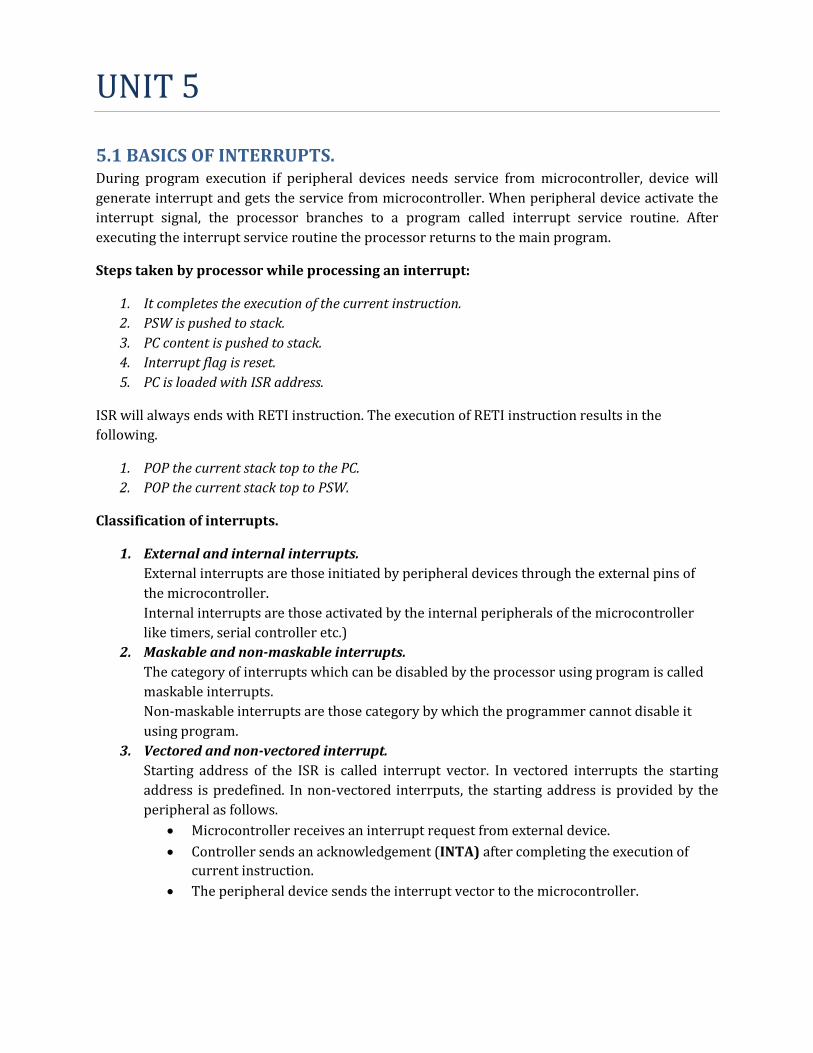
5.1 BASICS OF INTERRUPTS. During program execution if peripheral devices needs service from microcontroller, device will generate interrupt and gets the service from microcontroller. When peripheral device activate the interrupt signal, the processor branches to a program called interrupt service routine. After executing the interrupt service routine the processor returns to the main program. Steps taken by processor while processing an interrupt:
1. It completes the execution of the current instruction. 2. PSW is pushed to stack. 3. PC content is pushed to stack. 4. Interrupt flag is reset. 5. PC is loaded with ISR address.
ISR will always ends with RETI instruction. The execution of RETI instruction results in the following.
1. POP the current stack top to the PC. 2. POP the current stack top to PSW.
Classification of interrupts.
1. External and internal interrupts. External interrupts are those initiated by peripheral devices through the external pins of the microcontroller. Internal interrupts are those activated by the internal peripherals of the microcontroller like timers, serial controller etc.)
2. Maskable and non-maskable interrupts. The category of interrupts which can be disabled by the processor using program is called maskable interrupts. Non-maskable interrupts are those category by which the programmer cannot disable it using program.
3. Vectored and non-vectored interrupt. Starting address of the ISR is called interrupt vector. In vectored interrupts the starting address is predefined. In non-vectored interrputs, the starting address is provided by the peripheral as follows.
• Microcontroller receives an interrupt request from external device. • Controller sends an acknowledgement (INTA) after completing the execution of
current instruction. • The peripheral device sends the interrupt vector to the microcontroller.
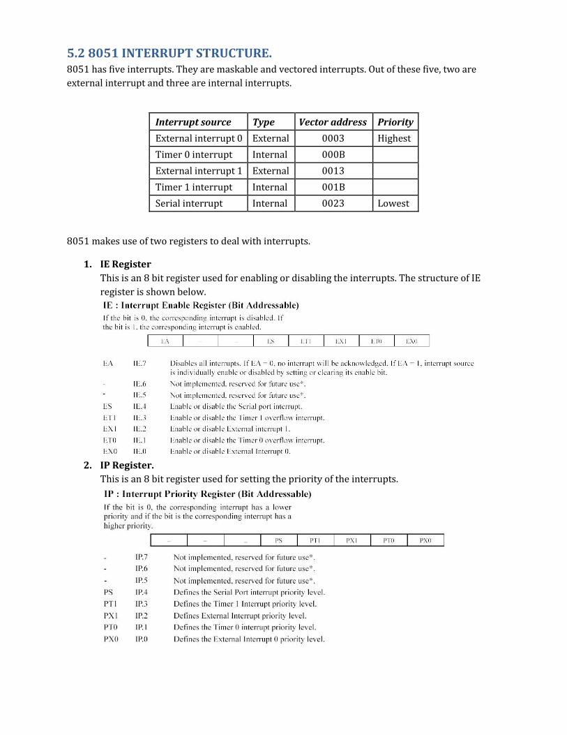
5.2 8051 INTERRUPT STRUCTURE. 8051 has five interrupts. They are maskable and vectored interrupts. Out of these five, two are external interrupt and three are internal interrupts.
Interrupt source Type Vector address Priority
External interrupt 0 External 0003 Highest
Timer 0 interrupt Internal 000B
External interrupt 1 External 0013
Timer 1 interrupt Internal 001B
Serial interrupt Internal 0023 Lowest
8051 makes use of two registers to deal with interrupts.
1. IE Register This is an 8 bit register used for enabling or disabling the interrupts. The structure of IE register is shown below.
2. IP Register. This is an 8 bit register used for setting the priority of the interrupts.
5.2 TIMERS AND COUNTERS Timers/Counters are used generally for
• Time reference • Creating delay • Wave form properties measurement • Periodic interrupt generation • Waveform generation
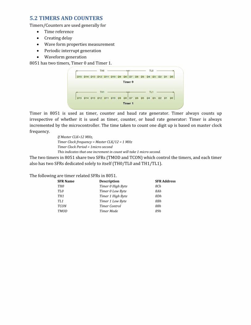
8051 has two timers, Timer 0 and Timer 1.
Timer in 8051 is used as timer, counter and baud rate generator. Timer always counts up irrespective of whether it is used as timer, counter, or baud rate generator: Timer is always incremented by the microcontroller. The time taken to count one digit up is based on master clock frequency.
If Master CLK=12 MHz, Timer Clock frequency = Master CLK/12 = 1 MHz Timer Clock Period = 1micro second This indicates that one increment in count will take 1 micro second.
The two timers in 8051 share two SFRs (TMOD and TCON) which control the timers, and each timer also has two SFRs dedicated solely to itself (TH0/TL0 and TH1/TL1). The following are timer related SFRs in 8051.
SFR Name Description SFR Address TH0 Timer 0 High Byte 8Ch TL0 Timer 0 Low Byte 8Ah TH1 Timer 1 High Byte 8Dh TL1 Timer 1 Low Byte 8Bh TCON Timer Control 88h TMOD Timer Mode 89h
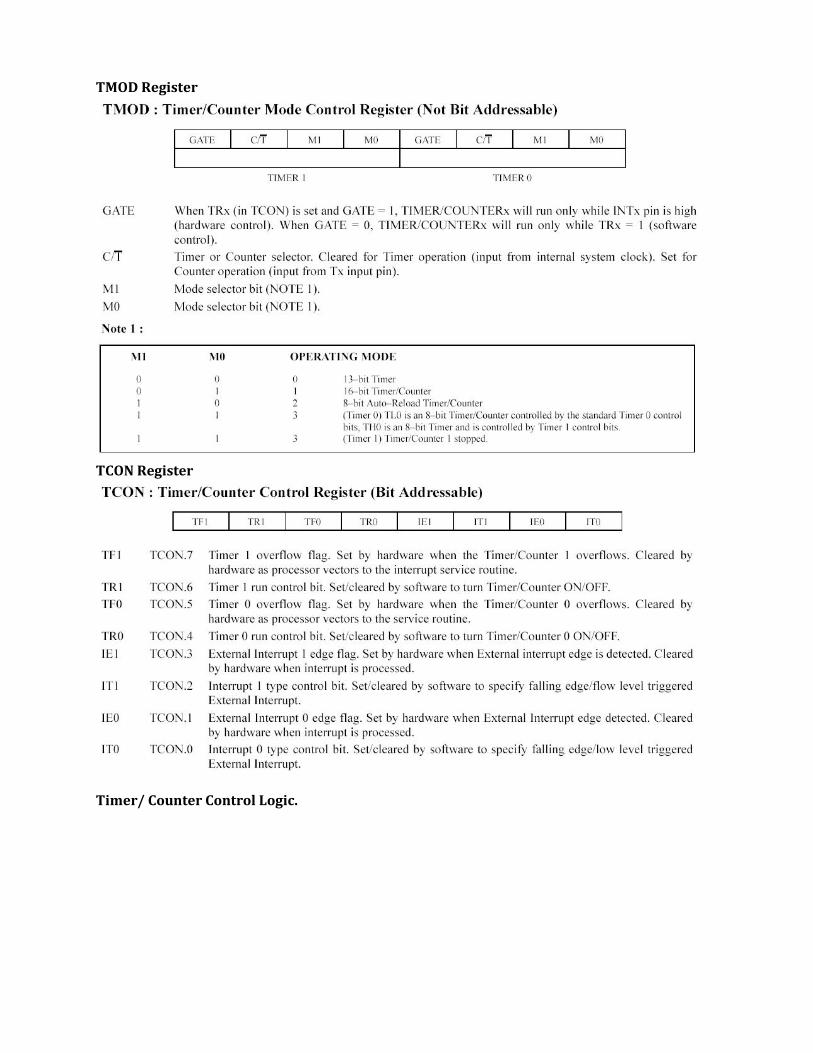
TMOD Register TCON Register Timer/ Counter Control Logic.
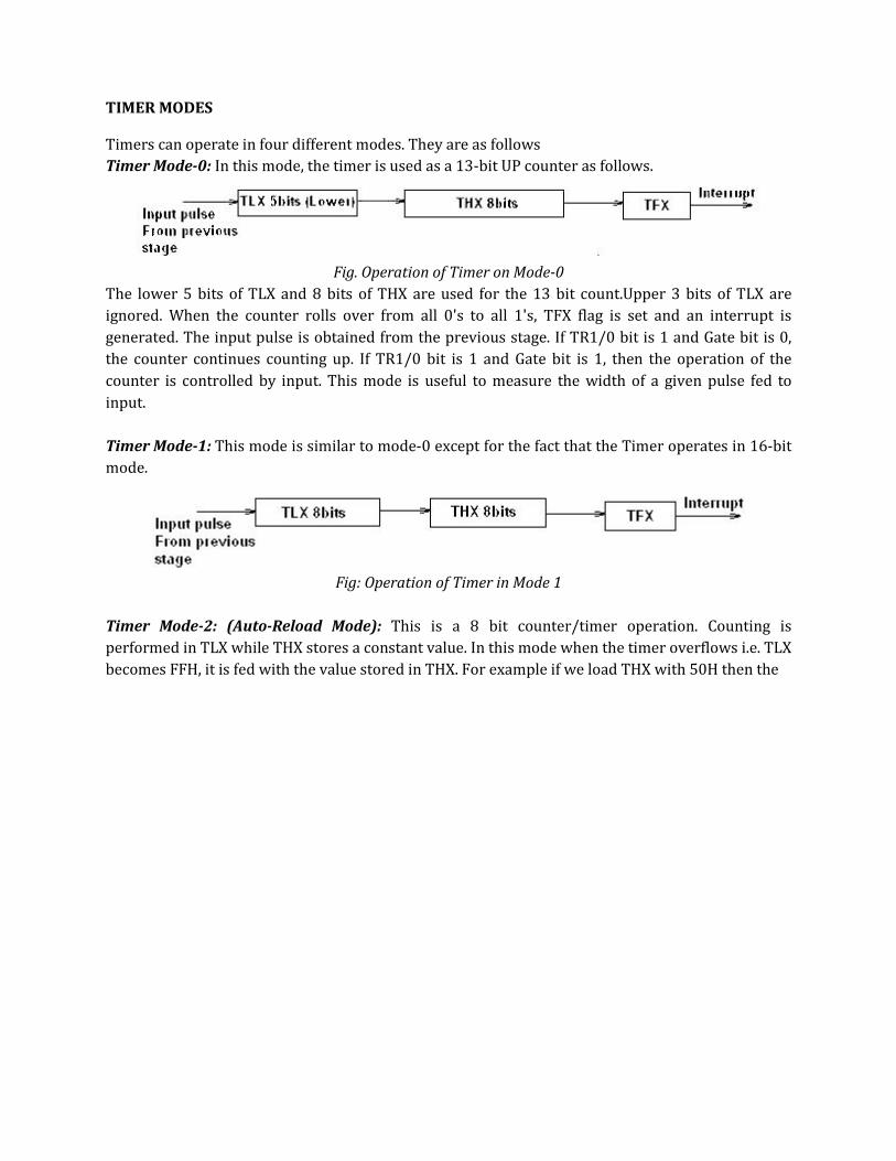
TIMER MODES Timers can operate in four different modes. They are as follows Timer Mode-0: In this mode, the timer is used as a 13-bit UP counter as follows.
Fig. Operation of Timer on Mode-0
The lower 5 bits of TLX and 8 bits of THX are used for the 13 bit count.Upper 3 bits of TLX are ignored. When the counter rolls over from all 0's to all 1's, TFX flag is set and an interrupt is generated. The input pulse is obtained from the previous stage. If TR1/0 bit is 1 and Gate bit is 0, the counter continues counting up. If TR1/0 bit is 1 and Gate bit is 1, then the operation of the counter is controlled by input. This mode is useful to measure the width of a given pulse fed to input. Timer Mode-1: This mode is similar to mode-0 except for the fact that the Timer operates in 16-bit mode.
Fig: Operation of Timer in Mode 1 Timer Mode-2: (Auto-Reload Mode): This is a 8 bit counter/timer operation. Counting is performed in TLX while THX stores a constant value. In this mode when the timer overflows i.e. TLX becomes FFH, it is fed with the value stored in THX. For example if we load THX with 50H then the
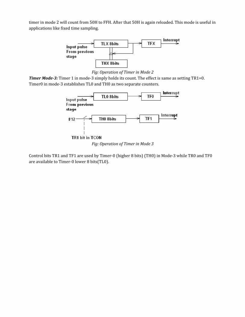
timer in mode 2 will count from 50H to FFH. After that 50H is again reloaded. This mode is useful in applications like fixed time sampling.
Fig: Operation of Timer in Mode 2 Timer Mode-3: Timer 1 in mode-3 simply holds its count. The effect is same as setting TR1=0. Timer0 in mode-3 establishes TL0 and TH0 as two separate counters.
Fig: Operation of Timer in Mode 3 Control bits TR1 and TF1 are used by Timer-0 (higher 8 bits) (TH0) in Mode-3 while TR0 and TF0 are available to Timer-0 lower 8 bits(TL0).
5.2 PROGRAMMING 8051 TIMERS IN ASSEMBLY In order to program 8051 timers, it is important to know the calculation of initial count value to be stored in the timer register. The calculations are as follows. In any mode, Timer Clock period = 1/Timer Clock Frequency.
= 1/(Master Clock Frequency/12)
a. Mode 1 (16 bit timer/counter) Value to be loaded in decimal = 65536 – (Delay Required/Timer clock period) Convert the answer into hexadecimal and load onto THx and TLx register. (65536D = FFFFH+1)
b. Mode 0 (13 bit timer/counter) Value to be loaded in decimal = 8192 – (Delay Required/Timer clock period) Convert the answer into hexadecimal and load onto THx and TLx register. (8192D = 1FFFH+1)
c. Mode 2 (8 bit auto reload) Value to be loaded in decimal = 256 – (Delay Required/Timer clock period) Convert the answer into hexadecimal and load onto THx register. Upon starting the timer this value from THx will be reloaded to TLx register. (256D = FFH+1)
Steps for programming timers in 8051
Mode 1: • Load the TMOD value register indicating which timer (0 or 1) is to be used and
which timer mode is selected. • Load registers TL and TH with initial count values. • Start the timer by the instruction “SETB TR0” for timer 0 and “SETB TR1” for timer 1. • Keep monitoring the timer flag (TF) with the “JNB TFx,target” instruction to see if it
is raised. Get out of the loop when TF becomes high. • Stop the timer with the instructions “CLR TR0” or “CLR TR1”, for timer 0 and timer
1, respectively. • Clear the TF flag for the next round with the instruction “CLR TF0” or “CLR TF1”,
for timer 0 and timer 1, respectively. • Go back to step 2 to load TH and TL again.
The programming techniques mentioned here are also applicable to counter/timer mode 0. The only difference is in the number of bits of the initialization value.
• Load the TMOD value register indicating which timer (0 or 1) is to be used; select
timer mode 2. • Load TH register with the initial count value. As it is an 8-bit timer, the valid range
is from 00 to FFH. • Start the timer.
• Keep monitoring the timer flag (TFx) with the “JNB TFx,target” instruction to see if it is raised. Get out of the loop when TFx goes high.
• Clear the TFx flag. • Go back to step 4, since mode 2 is auto-reload.
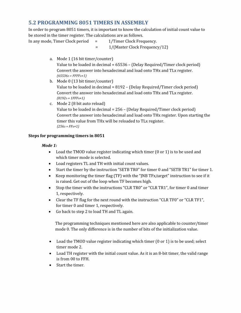
1. Write a program to continuously generate a square wave of 2 kHz frequency on pin
P1.5 using timer 1. Assume the crystal oscillator frequency to be 12 MHz.
The period of the square wave is T = 1/(2 kHz) = 500 µs. Each half pulse = 250 µs. The value n for 250 µs is: 250 µs /1 µs = 250 65536 - 250 = FF06H.
TL = 06H and TH = 0FFH.
MOV TMOD,#10 ;Timer 1, mode 1 AGAIN: MOV TL1,#06H ;TL0 = 06H MOV TH1,#0FFH ;TH0 = FFH SETB TR1 ;Start timer 1 BACK: JNB TF1,BACK ;Stay until timer rolls over CLR TR1 ;Stop timer 1 CPL P1.5 ;Complement P1.5 to get Hi, Lo CLR TF1 ;Clear timer flag 1 SJMP AGAIN ;Reload timer
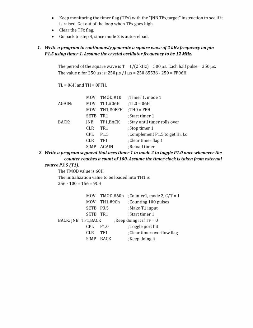
2. Write a program segment that uses timer 1 in mode 2 to toggle P1.0 once whenever the counter reaches a count of 100. Assume the timer clock is taken from external
source P3.5 (T1). The TMOD value is 60H The initialization value to be loaded into TH1 is 256 - 100 = 156 = 9CH
MOV TMOD,#60h ;Counter1, mode 2, C/T’= 1 MOV TH1,#9Ch ;Counting 100 pulses SETB P3.5 ;Make T1 input SETB TR1 ;Start timer 1
BACK: JNB TF1,BACK ;Keep doing it if TF = 0 CPL P1.0 ;Toggle port bit CLR TF1 ;Clear timer overflow flag SJMP BACK ;Keep doing it
UNIT 6
6.1 SERIAL COMMUNICATION. 6.1.1. DATA COMMUNICATION
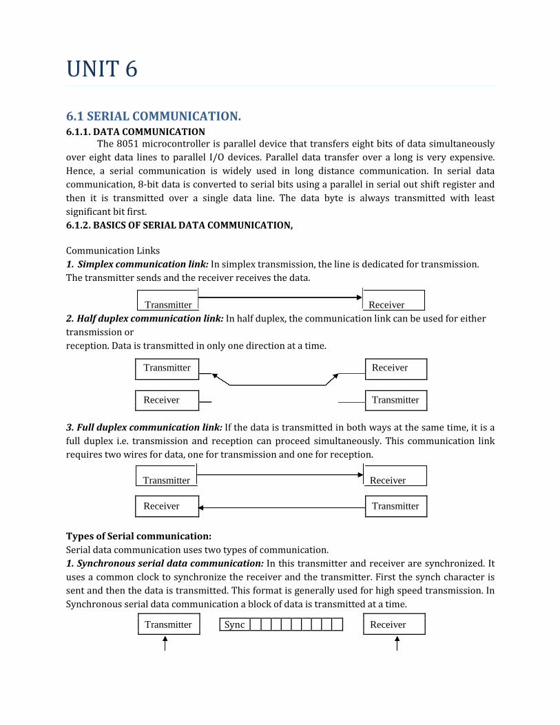
The 8051 microcontroller is parallel device that transfers eight bits of data simultaneously over eight data lines to parallel I/O devices. Parallel data transfer over a long is very expensive. Hence, a serial communication is widely used in long distance communication. In serial data communication, 8-bit data is converted to serial bits using a parallel in serial out shift register and then it is transmitted over a single data line. The data byte is always transmitted with least significant bit first. 6.1.2. BASICS OF SERIAL DATA COMMUNICATION, Communication Links 1. Simplex communication link: In simplex transmission, the line is dedicated for transmission. The transmitter sends and the receiver receives the data.
Transmitter Receiver 2. Half duplex communication link: In half duplex, the communication link can be used for either transmission or reception. Data is transmitted in only one direction at a time.
Transmitter Receiver
Receiver Transmitter
3. Full duplex communication link: If the data is transmitted in both ways at the same time, it is a full duplex i.e. transmission and reception can proceed simultaneously. This communication link requires two wires for data, one for transmission and one for reception.
Transmitter Receiver
Receiver Transmitter
Types of Serial communication: Serial data communication uses two types of communication. 1. Synchronous serial data communication: In this transmitter and receiver are synchronized. It uses a common clock to synchronize the receiver and the transmitter. First the synch character is sent and then the data is transmitted. This format is generally used for high speed transmission. In Synchronous serial data communication a block of data is transmitted at a time.
Transmitter Sync Receiver
Data Clock
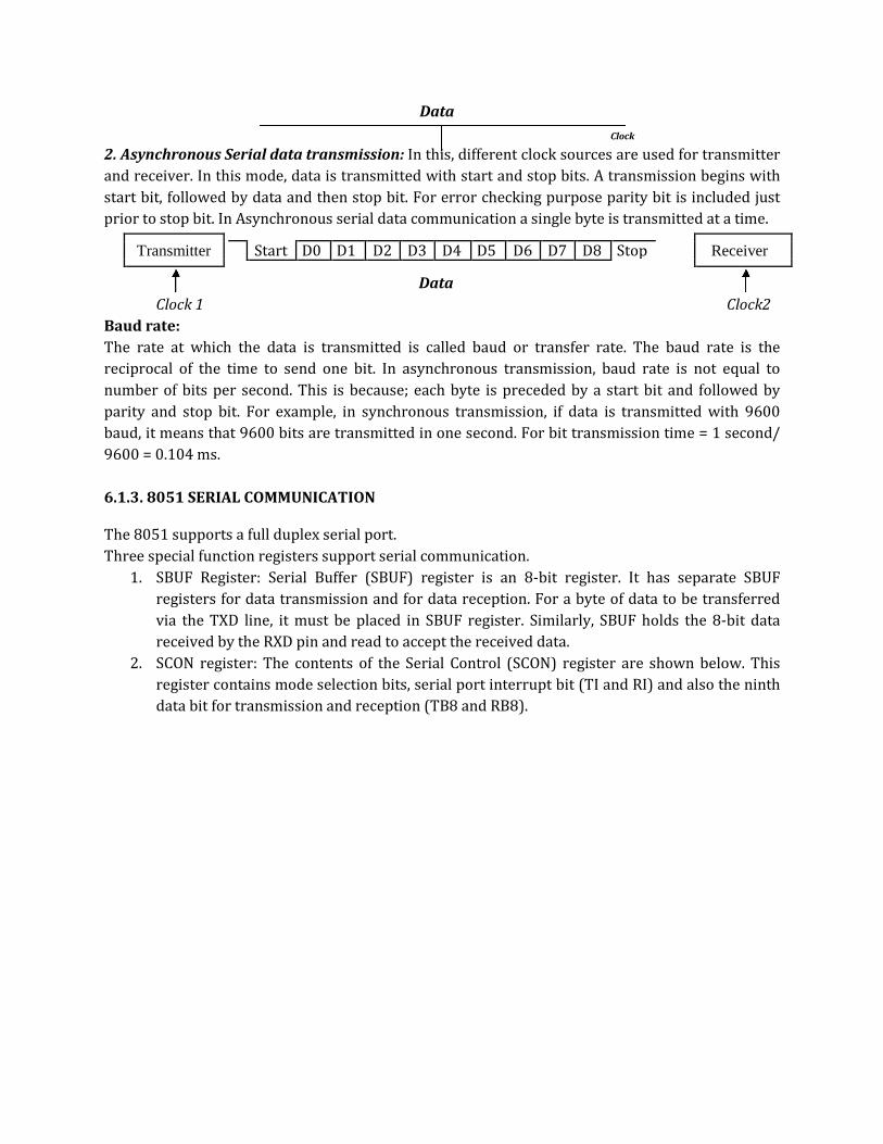
2. Asynchronous Serial data transmission: In this, different clock sources are used for transmitter and receiver. In this mode, data is transmitted with start and stop bits. A transmission begins with start bit, followed by data and then stop bit. For error checking purpose parity bit is included just prior to stop bit. In Asynchronous serial data communication a single byte is transmitted at a time.
Transmitter Start D0 D1 D2 D3 D4 D5 D6 D7 D8 Stop Receiver
Data
Clock 1 Clock2
Baud rate: The rate at which the data is transmitted is called baud or transfer rate. The baud rate is the reciprocal of the time to send one bit. In asynchronous transmission, baud rate is not equal to number of bits per second. This is because; each byte is preceded by a start bit and followed by parity and stop bit. For example, in synchronous transmission, if data is transmitted with 9600 baud, it means that 9600 bits are transmitted in one second. For bit transmission time = 1 second/ 9600 = 0.104 ms. 6.1.3. 8051 SERIAL COMMUNICATION The 8051 supports a full duplex serial port. Three special function registers support serial communication.
1. SBUF Register: Serial Buffer (SBUF) register is an 8-bit register. It has separate SBUF registers for data transmission and for data reception. For a byte of data to be transferred via the TXD line, it must be placed in SBUF register. Similarly, SBUF holds the 8-bit data received by the RXD pin and read to accept the received data.
2. SCON register: The contents of the Serial Control (SCON) register are shown below. This register contains mode selection bits, serial port interrupt bit (TI and RI) and also the ninth data bit for transmission and reception (TB8 and RB8).
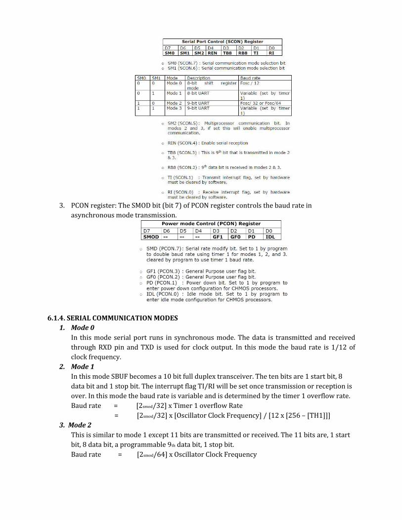
3. PCON register: The SMOD bit (bit 7) of PCON register controls the baud rate in
asynchronous mode transmission. 6.1.4. SERIAL COMMUNICATION MODES
1. Mode 0 In this mode serial port runs in synchronous mode. The data is transmitted and received through RXD pin and TXD is used for clock output. In this mode the baud rate is 1/12 of clock frequency.
2. Mode 1 In this mode SBUF becomes a 10 bit full duplex transceiver. The ten bits are 1 start bit, 8 data bit and 1 stop bit. The interrupt flag TI/RI will be set once transmission or reception is over. In this mode the baud rate is variable and is determined by the timer 1 overflow rate. Baud rate = [2smod/32] x Timer 1 overflow Rate
= [2smod/32] x [Oscillator Clock Frequency] / [12 x [256 – [TH1]]] 3. Mode 2
This is similar to mode 1 except 11 bits are transmitted or received. The 11 bits are, 1 start bit, 8 data bit, a programmable 9th data bit, 1 stop bit. Baud rate = [2smod/64] x Oscillator Clock Frequency
4. Mode 3
This is similar to mode 2 except baud rate is calculated as in mode 1 6.1.5. CONNECTIONS TO RS-232 RS-232 standards:
To allow compatibility among data communication equipment made by various manufactures, an interfacing standard called RS232 was set by the Electronics Industries Association (EIA) in 1960. Since the standard was set long before the advent of logic family, its input and output voltage levels are not TTL compatible.
In RS232, a logic one (1) is represented by -3 to -25V and referred as MARK while logic zero (0) is represented by +3 to +25V and referred as SPACE. For this reason to connect any RS232 to a microcontroller system we must use voltage converters such as MAX232 to convert the TTL logic level to RS232 voltage levels and vice-versa. MAX232 IC chips are commonly referred as line drivers.
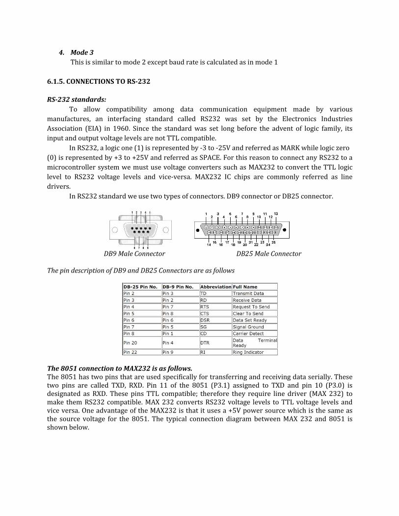
In RS232 standard we use two types of connectors. DB9 connector or DB25 connector.
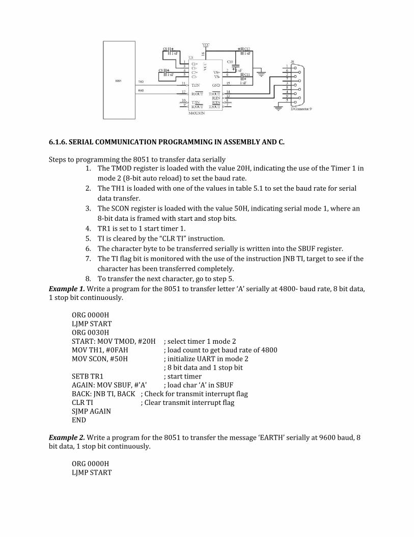
DB9 Male Connector DB25 Male Connector The pin description of DB9 and DB25 Connectors are as follows The 8051 connection to MAX232 is as follows. The 8051 has two pins that are used specifically for transferring and receiving data serially. These two pins are called TXD, RXD. Pin 11 of the 8051 (P3.1) assigned to TXD and pin 10 (P3.0) is designated as RXD. These pins TTL compatible; therefore they require line driver (MAX 232) to make them RS232 compatible. MAX 232 converts RS232 voltage levels to TTL voltage levels and vice versa. One advantage of the MAX232 is that it uses a +5V power source which is the same as the source voltage for the 8051. The typical connection diagram between MAX 232 and 8051 is shown below.
6.1.6. SERIAL COMMUNICATION PROGRAMMING IN ASSEMBLY AND C. Steps to programming the 8051 to transfer data serially
1. The TMOD register is loaded with the value 20H, indicating the use of the Timer 1 in mode 2 (8-bit auto reload) to set the baud rate.
2. The TH1 is loaded with one of the values in table 5.1 to set the baud rate for serial data transfer.
3. The SCON register is loaded with the value 50H, indicating serial mode 1, where an 8-bit data is framed with start and stop bits.
4. TR1 is set to 1 start timer 1. 5. TI is cleared by the “CLR TI” instruction. 6. The character byte to be transferred serially is written into the SBUF register. 7. The TI flag bit is monitored with the use of the instruction JNB TI, target to see if the
character has been transferred completely. 8. To transfer the next character, go to step 5.
Example 1. Write a program for the 8051 to transfer letter ‘A’ serially at 4800- baud rate, 8 bit data, 1 stop bit continuously.
ORG 0000H LJMP START ORG 0030H START: MOV TMOD, #20H ; select timer 1 mode 2 MOV TH1, #0FAH ; load count to get baud rate of 4800 MOV SCON, #50H ; initialize UART in mode 2 ; 8 bit data and 1 stop bit SETB TR1 ; start timer AGAIN: MOV SBUF, #'A' ; load char ‘A’ in SBUF BACK: JNB TI, BACK ; Check for transmit interrupt flag CLR TI ; Clear transmit interrupt flag SJMP AGAIN END
Example 2. Write a program for the 8051 to transfer the message ‘EARTH’ serially at 9600 baud, 8 bit data, 1 stop bit continuously.
ORG 0000H LJMP START
ORG 0030H START: MOV TMOD, #20H MOV TH1, #0FDH MOV SCON, #50H
SETB TR1 LOOP: MOV A, #'E' ACALL LOAD MOV A, #'A' ACALL LOAD MOV A, #'R' ACALL LOAD MOV A, #'T' ACALL LOAD MOV A, #'H' ACALL LOAD SJMP LOOP
; select timer 1 mode 2 ; load count to get reqd. baud rate of 9600 ; initialise uart in mode 2 ; 8 bit data and 1 stop bit ; start timer
; load 1st letter ‘E’ in a ; call load subroutine
; load 2nd letter ‘A’ in a ; call load subroutine
; load 3rd letter ‘R’ in a ; call load subroutine
; load 4th letter ‘T’ in a ; call load subroutine
; load 4th letter ‘H’ in a ; call load subroutine ; repeat steps
LOAD: MOV SBUF, A HERE: JNB TI, HERE ; Check for transmit interrupt flag
CLR TI ; Clear transmit interrupt flag RET
END
6.2 8255A PROGRAMMABLE PERIPHERAL INTERFACE Introduction The 8255A programmable peripheral interface (PPI) implements a general-purpose I/O interface to connect peripheral equipment to a microcomputer system bus. Features
• Three 8-bit Peripheral Ports - Ports A, B, and C • Three programming modes for Peripheral Ports: Mode 0 (Basic Input/Output), Mode 1
(Strobed Input/Output), and Mode 2 (Bidirectional) • Total of 24 programmable I/O lines • 8-bit bidirectional system data bus with standard microprocessor interface controls
6.2.1. ARCHITECTURE OF 8255A
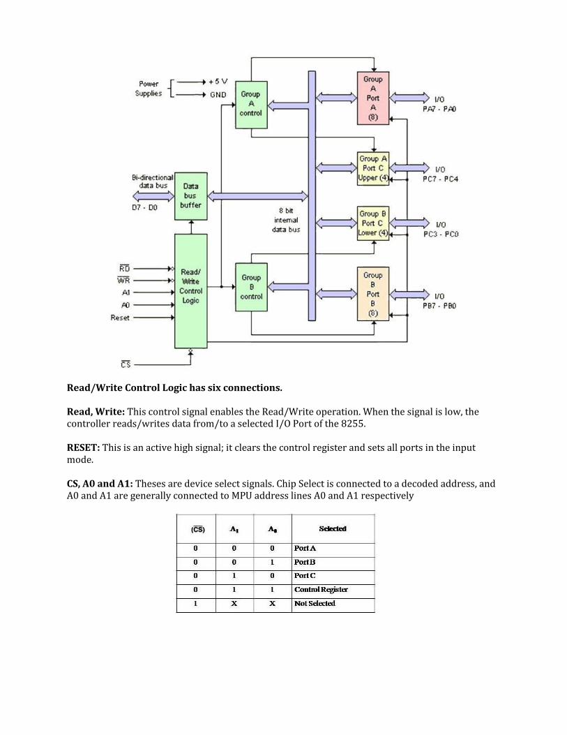
Read/Write Control Logic has six connections. Read, Write: This control signal enables the Read/Write operation. When the signal is low, the controller reads/writes data from/to a selected I/O Port of the 8255. RESET: This is an active high signal; it clears the control register and sets all ports in the input mode. CS, A0 and A1: Theses are device select signals. Chip Select is connected to a decoded address, and A0 and A1 are generally connected to MPU address lines A0 and A1 respectively
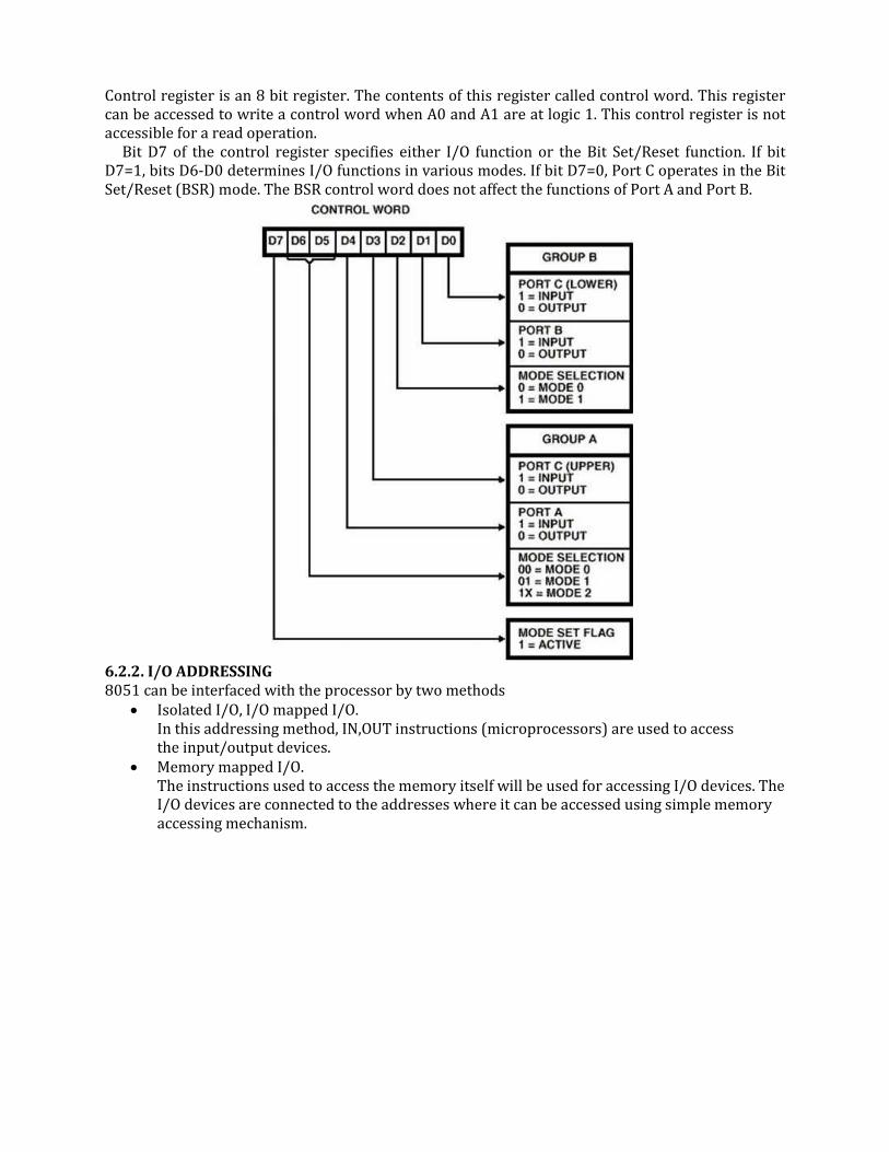
Control register is an 8 bit register. The contents of this register called control word. This register can be accessed to write a control word when A0 and A1 are at logic 1. This control register is not accessible for a read operation.
Bit D7 of the control register specifies either I/O function or the Bit Set/Reset function. If bit D7=1, bits D6-D0 determines I/O functions in various modes. If bit D7=0, Port C operates in the Bit Set/Reset (BSR) mode. The BSR control word does not affect the functions of Port A and Port B. 6.2.2. I/O ADDRESSING 8051 can be interfaced with the processor by two methods
• Isolated I/O, I/O mapped I/O. In this addressing method, IN,OUT instructions (microprocessors) are used to access the input/output devices.
• Memory mapped I/O. The instructions used to access the memory itself will be used for accessing I/O devices. The I/O devices are connected to the addresses where it can be accessed using simple memory accessing mechanism.