Embed Size (px)
Citation preview
HAL Id: lirmm-01867729https://hal-lirmm.ccsd.cnrs.fr/lirmm-01867729
Submitted on 4 Sep 2018
HAL is a multi-disciplinary open accessarchive for the deposit and dissemination of sci-entific research documents, whether they are pub-lished or not. The documents may come fromteaching and research institutions in France orabroad, or from public or private research centers.
L’archive ouverte pluridisciplinaire HAL, estdestinée au dépôt et à la diffusion de documentsscientifiques de niveau recherche, publiés ou non,émanant des établissements d’enseignement et derecherche français ou étrangers, des laboratoirespublics ou privés.
Understanding Electromigration in Cu-CNT CompositeInterconnects: A Multiscale Electrothermal Simulation
StudyJaehyun Lee, Salim Berrada, Fikru Adamu-Lema, Nicole Nagy, Vihar P.
Georgiev, Toufik Sadi, Jie Liang, Raphael Ramos, Hamilton Carrillo-Nunez,Dipankar Kalita, et al.
To cite this version:Jaehyun Lee, Salim Berrada, Fikru Adamu-Lema, Nicole Nagy, Vihar P. Georgiev, et al.. Understand-ing Electromigration in Cu-CNT Composite Interconnects: A Multiscale Electrothermal SimulationStudy. IEEE Transactions on Electron Devices, Institute of Electrical and Electronics Engineers,2018, 65 (9), pp.3884-3892. 10.1109/TED.2018.2853550. lirmm-01867729
JOURNAL OF LATEX CLASS FILES, VOL. 14, NO. 8, AUGUST 2017 1
Understanding Electromigration in Cu-CNTComposite Interconnects: A Multiscale
Electro-Thermal Simulation StudyJaehyun Lee, Salim Berrada, Fikru Adamu-Lema, Nicole Nagy, Vihar P. Georgiev, Toufik Sadi, Jie Liang,
Raphael Ramos, Hamilton Carrillo-Nunez, Dipankar Kalita, Katharina Lilienthal, Marcus Wislicenus,Reeturaj Pandey, Bingan Chen, Kenneth B. K. Teo, Goncalo Goncalves, Hanako Okuno, Benjamin Uhlig, Aida
Todri-Sanial, Jean Dijon, and Asen Asenov, Fellow, IEEE
Abstract—In this paper, we report a hierarchical simulationstudy on the electromigration problem in Cu-CNT compositeinterconnects. Our work is based on the investigation of theactivation energy and self-heating temperature using a multiscaleelectro-thermal simulation framework. We first investigate theelectrical and thermal properties of Cu-CNT composites includ-ing contact resistances using the Density Functional Theory andReactive Force Field approaches, respectively. The correspondingresults are employed in macroscopic electro-thermal simulationstaking into account the self-heating phenomenon. Our simu-lations show that although Cu atoms have similar activationenergies in both bulk Cu and Cu-CNT composites, Cu-CNTcomposite interconnects are more resistant to electromigrationthanks to the large Lorenz number of the CNTs. Moreover,we found that a large and homogenous conductivity along thetransport direction in interconnects is one of the most importantdesign rules to minimize the electromigration.
Index Terms—Cu-CNT composites, Interconnect, Electromi-gration, Self-heating, Electro-thermal coupling, DFT, Multi-scalesimulation
I. INTRODUCTION
DUAL damascene process technology with proper barriermetals such as TaN has been successfully used to fabri-
cate Cu interconnects for the past 20 years [1]–[3]. However,aggressive scaling of dimensions of microchips results in anincrease of the resistance in Cu interconnects due to thegrain boundary (GBS) and the surface roughness scatterings(SRS) [4]–[6]. Increased resistance of the interconnect causesincreased interconnect delay [7]. Moreover, many types of
This work was supported by the European Commission EU2020 CON-NECT project under grant agreement number 688612.
J.Lee, S. Berrada, F. Adamu-Lema, V. P. Georgiev, H. Carrillo-Nunez, andA. Asenov are with School of Engineering, University of Glasgow, Glasgow,G12 8QQ UK e-mail: [email protected]
N. Nagy, K. Lilienthal, M. Wislicenus, and B. Uhlig are with CenterNanoelectronic Technologies Department, Fraunhofer, IPMS, 01099 Dresden,Germany
T. Sadi is with the Department of Neuroscience and Biomedical Engineer-ing, Aalto University, P.O. Box 12200, FI-00076 AALTO, Finland
R. Ramos and J. Dijon are with Nanomaterials Department, CEA-LITEN,University of Grenoble Alpes, Grenoble, 38000 France
J. Liang, R. Pandey, and A. Todri-Sanial are with Microelectronics Depart-ment, CNRS-LIRMM, Montpellier, 34095 France
D. Kalita and H. Okunol are with Nanomaterials Department, CEA-INAC,University Grenoble Alpes, Grenoble, 38000 France
B. Chen, K. B. K. Teo, and G. Goncalves are with NanoinstrumentsDepartment, AIXTRON Ltd, Cambridge, CB24 4FQ UK
Manuscript received
reliability issues arise during both manufacturing process, suchas defects and voids [8], and the operation of the device,such as electromigration (EM) [9]–[12]. It is also well-knownthat the power consumption increases when scaling down theinterconnect [13]. Nowadays, these issues must be consideredcarefully, since the overall performance and reliability of chipsare dominated by interconnects [14], [15].
For more than a decade, carbon-based interconnects haveattracted attention as a potential future interconnect technologyto overcome some of these problems – GBS, SRS, and elec-tromigration [16]–[22]. Indeed, carbon nanotubes (CNTs) andgraphene show high ampacity (maximum current-carrying-capacity) and thermal conductivity thanks to their strong C-Cbonding [23]–[25]. Ampacity is one of the key figures used toquantify EM. In particular, to prevent capacitance build-up bythe barrier metal, Li et al. used single- or bi-layer graphene asthe Cu diffusion barrier in Cu interconnects and successfullydemonstrated their smaller resistivity and longer EM lifetime[26].
More promising results were shown by Subramaniam etal. in 2013 with CNTs [19]. They reported that Cu-CNTcomposite interconnects without the diffusion barrier can havenot only a similar conductivity to Cu interconnects but alsoa 100 times better ampacity than Cu interconnects. However,an in-depth analysis of the migration reduction of Cu atomsin Cu-CNT composite interconnects is still lacking.
In this paper, we present a multi-scale electro-thermal simu-lation study to understand the electromigration phenomenon inCu-CNT composite interconnects. In general, EM in intercon-nects can be characterized by the Time-To-Fail figure (TTF ),whose expression is given by Black’s equation [27]:
TTF = A∗J−reEa/(kBT ) (1)
where A∗ is an empirical constant, J is the current density,r is a positive dimensionless exponent, kB is the Boltzmannconstant, Ea is the activation energy, and T is the temperatureof the interconnect. According to Eq. 1, there are two waysto obtain a larger current density while maintaining the sameTTF . The first option is to increase the activation energy.To do this, the diffusion barrier with appropriate properties isadopted in the standard Cu interconnect [3]. The second wayis to decrease T , which can be achieved by suppressing theself-heating effects. Unfortunately, decreasing T is difficult
JOURNAL OF LATEX CLASS FILES, VOL. 14, NO. 8, AUGUST 2017 2
because the self-heating temperature T is caused by highJ or high applied voltage (V ) during the chip operation.For this reason, we implemented heat diffusion equation[28] in our simulation framework to capture the self-heatingeffects. Finally, from all simulation results, we provide designguidelines to optimize the performance of Cu-CNT compositeinterconnects.
This paper is organized as follow. Section II shows thefirst principle simulation results of the activation energy andthe contact resistance between Cu and CNT. In Section III,we examine the self-heating temperature of Cu and Cu-CNTcomposite interconnects using the first principle calculationresults. In Section IV, we provide the optimal design guidelinesfor Cu-CNT composite interconnects. Finally, conclusions aredrawn in Section V.
II. FIRST PRINCIPLE SIMULATION
We investigated the electrical and thermal properties of Cu-CNT composite interconnects using the Density FunctionalTheory (DFT) and the Reactive Force Field (ReaxFF) methods,respectively [29]–[33]. Both methods are implemented in theAtomistix Tool Kit (ATK) from QuantumWise [34]. Theatomistic structures are optimized until the maximum force ofeach atom becomes less than 10−2 eV/A for electrical (DFT)and 10−4 eV/A for thermal (ReaxFF) analysis, respectively.For the DFT calculations, we use the Generalized GradientApproximation (GGA) as the exchange-correlation functional,as proposed by Perdew, Burke, and Ernzerhof [35]. The norm-conserving pseudopotentials generated with the Fritz-HaberInstitute pseudopotential code are used with the double-ζsingly-polarized pseudoatomic orbital basis set. The toleranceof the self-consistent field loop calculation is set 10−4.
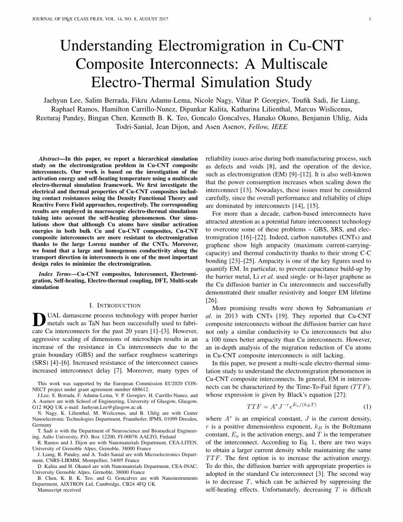
Fig. 1 illustrates examples of optimized atomistic structuresof Cu-CNT(4,4) and Cu-CNT(6,0) composites. The lattice ori-entation of a Cu part is selected to reduce the lattice mismatchwith CNT along the transport direction. We assume that CNTis not strained by Cu in this study. The lattice parameters ofbulk Cu, zigzag CNT(6,0), and armchair CNT(4,4) in DFT-GGA calculations are 3.670, 4.280, 2.474 A, respectively. Inaddition, we placed Cu atoms to prevent the CNT from beingdistorted severely.
A. Acitvation energy
The activation energy Ea in Eq. 1, which is the energy re-quired for a thermo-dynamic reaction to occur, is an importantparameter to describe the EM phenomenon. In general, thestructure with low value of the activation energy is vulnerableto the EM. In 2013, measurements of TTF by Subramaniamet al. [19] showed that Cu-CNT composite interconnectsexhibit much better EM properties than their Cu counterpart.They attributed this outperformance to the enhancement ofCu’s activation energy thanks to the presence of C atoms.Nevertheless, considering the weak van der Waals interactionat the interface between Cu and CNT, it is difficult to seehow the presence of the CNT could enhance the activationenergy of Cu atoms at its interface. Moreover, in a Cu-CNTcomposite, there is not only a Cu-CNT interface but also a
Fig. 1. Atomistic structures of a) Cu-CNT(4,4) and b) Cu-CNT(6,0) com-posites. The blue and brown spheres are Cu and C atoms, respectively.
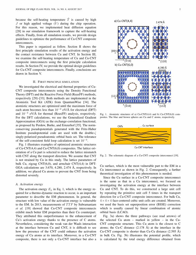
Fig. 2. The schematic diagram of a Cu-CNT composite interconnect [19].
Cu surface, which is the most vulnerable part to the EM in aCu interconnect as shown in Fig. 2. Consequently, a furthertheoretical investigation of this phenomenon is needed.
Since the Cu surface in a Cu-CNT composite interconnectis the same as that in a Cu interconnect, we focused oninvestigating the activation energy at the interface betweenCu and CNT. To do this, we constructed a large unit cellby repeating the primitive unit cell 5 times in the transportdirection for a Cu-CNT composite interconnect. For bulk Cu,4×4×4 face-centered cubic unit cells are created. Moreover,we used the basis set superposition error (BSSE) correctionwhich is usually caused by linear combination of atomicorbital basis (LCAO).
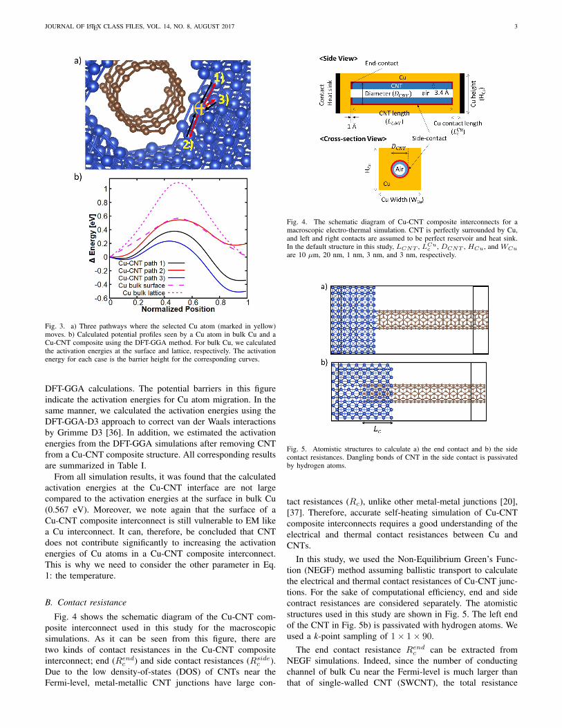
Fig. 3a) shows the three pathways (see read arrows) ofthe selected Cu atom – marked in yellow – in the Cu-CNT composite structure. This Cu atom is the closest to Catoms; the Cu-C distance (2.178 A) at the interface in theCu-CNT composite is shorter than Cu-Cu distance (2.595 A)in bulk Cu. Fig. 3b) illustrates the potential profile, whichis calculated by the total energy difference obtained from
JOURNAL OF LATEX CLASS FILES, VOL. 14, NO. 8, AUGUST 2017 3
Fig. 3. a) Three pathways where the selected Cu atom (marked in yellow)moves. b) Calculated potential profiles seen by a Cu atom in bulk Cu and aCu-CNT composite using the DFT-GGA method. For bulk Cu, we calculatedthe activation energies at the surface and lattice, respectively. The activationenergy for each case is the barrier height for the corresponding curves.
DFT-GGA calculations. The potential barriers in this figureindicate the activation energies for Cu atom migration. In thesame manner, we calculated the activation energies using theDFT-GGA-D3 approach to correct van der Waals interactionsby Grimme D3 [36]. In addition, we estimated the activationenergies from the DFT-GGA simulations after removing CNTfrom a Cu-CNT composite structure. All corresponding resultsare summarized in Table I.
From all simulation results, it was found that the calculatedactivation energies at the Cu-CNT interface are not largecompared to the activation energies at the surface in bulk Cu(0.567 eV). Moreover, we note again that the surface of aCu-CNT composite interconnect is still vulnerable to EM likea Cu interconnect. It can, therefore, be concluded that CNTdoes not contribute significantly to increasing the activationenergies of Cu atoms in a Cu-CNT composite interconnect.This is why we need to consider the other parameter in Eq.1: the temperature.
B. Contact resistance
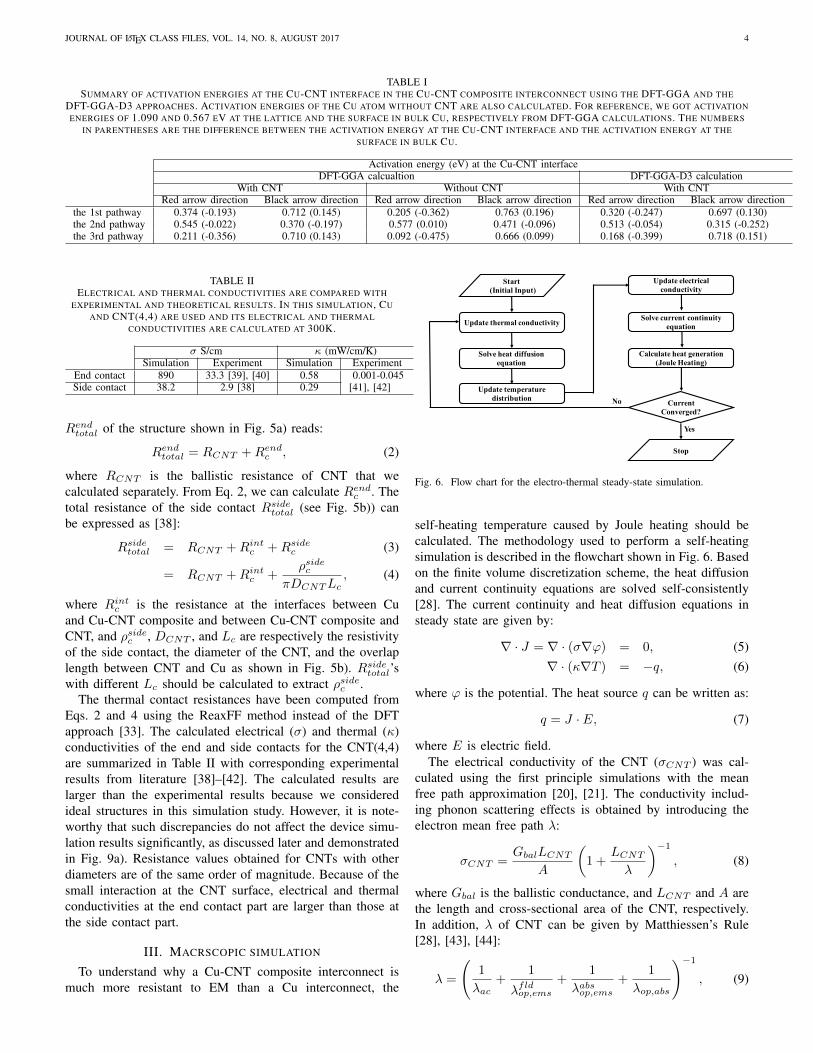
Fig. 4 shows the schematic diagram of the Cu-CNT com-posite interconnect used in this study for the macroscopicsimulations. As it can be seen from this figure, there aretwo kinds of contact resistances in the Cu-CNT compositeinterconnect; end (Rend
c ) and side contact resistances (Rsidec ).
Due to the low density-of-states (DOS) of CNTs near theFermi-level, metal-metallic CNT junctions have large con-
Fig. 4. The schematic diagram of Cu-CNT composite interconnects for amacroscopic electro-thermal simulation. CNT is perfectly surrounded by Cu,and left and right contacts are assumed to be perfect reservoir and heat sink.In the default structure in this study, LCNT , LCu
c , DCNT , HCu, and WCu
are 10 µm, 20 nm, 1 nm, 3 nm, and 3 nm, respectively.
Fig. 5. Atomistic structures to calculate a) the end contact and b) the sidecontact resistances. Dangling bonds of CNT in the side contact is passivatedby hydrogen atoms.
tact resistances (Rc), unlike other metal-metal junctions [20],[37]. Therefore, accurate self-heating simulation of Cu-CNTcomposite interconnects requires a good understanding of theelectrical and thermal contact resistances between Cu andCNTs.
In this study, we used the Non-Equilibrium Green’s Func-tion (NEGF) method assuming ballistic transport to calculatethe electrical and thermal contact resistances of Cu-CNT junc-tions. For the sake of computational efficiency, end and sidecontract resistances are considered separately. The atomisticstructures used in this study are shown in Fig. 5. The left endof the CNT in Fig. 5b) is passivated with hydrogen atoms. Weused a k-point sampling of 1× 1× 90.
The end contact resistance Rendc can be extracted from
NEGF simulations. Indeed, since the number of conductingchannel of bulk Cu near the Fermi-level is much larger thanthat of single-walled CNT (SWCNT), the total resistance
JOURNAL OF LATEX CLASS FILES, VOL. 14, NO. 8, AUGUST 2017 4
TABLE ISUMMARY OF ACTIVATION ENERGIES AT THE CU-CNT INTERFACE IN THE CU-CNT COMPOSITE INTERCONNECT USING THE DFT-GGA AND THE
DFT-GGA-D3 APPROACHES. ACTIVATION ENERGIES OF THE CU ATOM WITHOUT CNT ARE ALSO CALCULATED. FOR REFERENCE, WE GOT ACTIVATIONENERGIES OF 1.090 AND 0.567 EV AT THE LATTICE AND THE SURFACE IN BULK CU, RESPECTIVELY FROM DFT-GGA CALCULATIONS. THE NUMBERS
IN PARENTHESES ARE THE DIFFERENCE BETWEEN THE ACTIVATION ENERGY AT THE CU-CNT INTERFACE AND THE ACTIVATION ENERGY AT THESURFACE IN BULK CU.
Activation energy (eV) at the Cu-CNT interfaceDFT-GGA calcualtion DFT-GGA-D3 calculation
With CNT Without CNT With CNTRed arrow direction Black arrow direction Red arrow direction Black arrow direction Red arrow direction Black arrow direction
the 1st pathway 0.374 (-0.193) 0.712 (0.145) 0.205 (-0.362) 0.763 (0.196) 0.320 (-0.247) 0.697 (0.130)the 2nd pathway 0.545 (-0.022) 0.370 (-0.197) 0.577 (0.010) 0.471 (-0.096) 0.513 (-0.054) 0.315 (-0.252)the 3rd pathway 0.211 (-0.356) 0.710 (0.143) 0.092 (-0.475) 0.666 (0.099) 0.168 (-0.399) 0.718 (0.151)
TABLE IIELECTRICAL AND THERMAL CONDUCTIVITIES ARE COMPARED WITH
EXPERIMENTAL AND THEORETICAL RESULTS. IN THIS SIMULATION, CUAND CNT(4,4) ARE USED AND ITS ELECTRICAL AND THERMAL
CONDUCTIVITIES ARE CALCULATED AT 300K.
σ S/cm κ (mW/cm/K)Simulation Experiment Simulation Experiment
End contact 890 33.3 [39], [40] 0.58 0.001-0.045[41], [42]Side contact 38.2 2.9 [38] 0.29
Rendtotal of the structure shown in Fig. 5a) reads:
Rendtotal = RCNT +Rend
c , (2)
where RCNT is the ballistic resistance of CNT that wecalculated separately. From Eq. 2, we can calculate Rend
c . Thetotal resistance of the side contact Rside
total (see Fig. 5b)) canbe expressed as [38]:
Rsidetotal = RCNT +Rint
c +Rsidec (3)
= RCNT +Rintc +
ρsidec
πDCNTLc, (4)
where Rintc is the resistance at the interfaces between Cu
and Cu-CNT composite and between Cu-CNT composite andCNT, and ρsidec , DCNT , and Lc are respectively the resistivityof the side contact, the diameter of the CNT, and the overlaplength between CNT and Cu as shown in Fig. 5b). Rside
total’swith different Lc should be calculated to extract ρsidec .
The thermal contact resistances have been computed fromEqs. 2 and 4 using the ReaxFF method instead of the DFTapproach [33]. The calculated electrical (σ) and thermal (κ)conductivities of the end and side contacts for the CNT(4,4)are summarized in Table II with corresponding experimentalresults from literature [38]–[42]. The calculated results arelarger than the experimental results because we consideredideal structures in this simulation study. However, it is note-worthy that such discrepancies do not affect the device simu-lation results significantly, as discussed later and demonstratedin Fig. 9a). Resistance values obtained for CNTs with otherdiameters are of the same order of magnitude. Because of thesmall interaction at the CNT surface, electrical and thermalconductivities at the end contact part are larger than those atthe side contact part.
III. MACRSCOPIC SIMULATION
To understand why a Cu-CNT composite interconnect ismuch more resistant to EM than a Cu interconnect, the
Start(Initial Input)
Update thermal conductivity
Solve heat diffusion equation
Update temperature distribution
Update electrical conductivity
Solve current continuity equation
Calculate heat generation (Joule Heating)
Current Converged?
Stop
No
Yes
Fig. 6. Flow chart for the electro-thermal steady-state simulation.
self-heating temperature caused by Joule heating should becalculated. The methodology used to perform a self-heatingsimulation is described in the flowchart shown in Fig. 6. Basedon the finite volume discretization scheme, the heat diffusionand current continuity equations are solved self-consistently[28]. The current continuity and heat diffusion equations insteady state are given by:
∇ · J = ∇ · (σ∇ϕ) = 0, (5)∇ · (κ∇T ) = −q, (6)
where ϕ is the potential. The heat source q can be written as:
q = J · E, (7)
where E is electric field.The electrical conductivity of the CNT (σCNT ) was cal-
culated using the first principle simulations with the meanfree path approximation [20], [21]. The conductivity includ-ing phonon scattering effects is obtained by introducing theelectron mean free path λ:
σCNT =GbalLCNT
A
(1 +
LCNT
λ
)−1
, (8)
where Gbal is the ballistic conductance, and LCNT and A arethe length and cross-sectional area of the CNT, respectively.In addition, λ of CNT can be given by Matthiessen’s Rule[28], [43], [44]:
λ =
(1
λac+
1
λfldop,ems
+1
λabsop,ems
+1
λop,abs
)−1
, (9)
JOURNAL OF LATEX CLASS FILES, VOL. 14, NO. 8, AUGUST 2017 5
where λac, λfldop,ems, λabsop,ems, and λop,abs are the electron meanfree paths from acoustic phonon, optical phonon emission afterelectrons gained energy from the electric field, optical phononemission after absorption, and optical phonon absorption,respectively. These parameters can be calculated as following[43], [44]:
λac = 400460× DCNT
T
λop,abs = 56.4×DCNTNop(300) + 1
Nop(T )
λabsop,ems = λop,abs + 56.4×DCNTNop(300) + 1
Nop(T ) + 1
λfldop,ems =hωop − kBTqV/LCNT
+ 56.4×DCNTNop(300) + 1
Nop(T ) + 1
NOP (T ) = 1/exp((hωop)/(kBT ))−1 is the average opticalphonons number defined by the Bose-Einstein distribution, andhωop is the optical phonon energy. We set hωop to 0.18 eV inthis study [44]. The mean free path of CNTs is thus a functionof T , LCNT , DCNT , and V .
Using the linear approximation for resistivity, the electricalconductivity of Cu (σCu) is given by:
σCu(T ) =σ0
1 + α(T − T0)(10)
where T0 is a fixed reference temperature, 293 K, α =0.003862 K−1 is the temperature coefficient of resistivity andσ0 is the conductivity at T0. σ0 for Cu will be discussed inthe next subsection.
We compute the thermal conductivity κ for both Cu andCNT using Wiedemann-Franzs law [45]:
κ = σLT, (11)
where L is the Lorenz number. The values we used for L inthis study are 2.23×10⁻⁸ WΩK−2 for Cu [46] and 4.0×10⁻⁶
WΩK−2 for CNT [23]. L of the CNT is about 180 times largerthan that of Cu, meaning that the thermal condcutivity κ of theCNT is mostly dominated by phonons (as opposed to Cu whereκ is dominated by electrons). In this study, we did not considerheat dissipation through the environment of the interconnectsand the calculated T may thus be overestimated. However, thisis a global effect affecting all the interconnects considered hereand therefore, our study ensures a good comparison betweenthem.
A. Scattering effects in nanoscale Cu interconnect
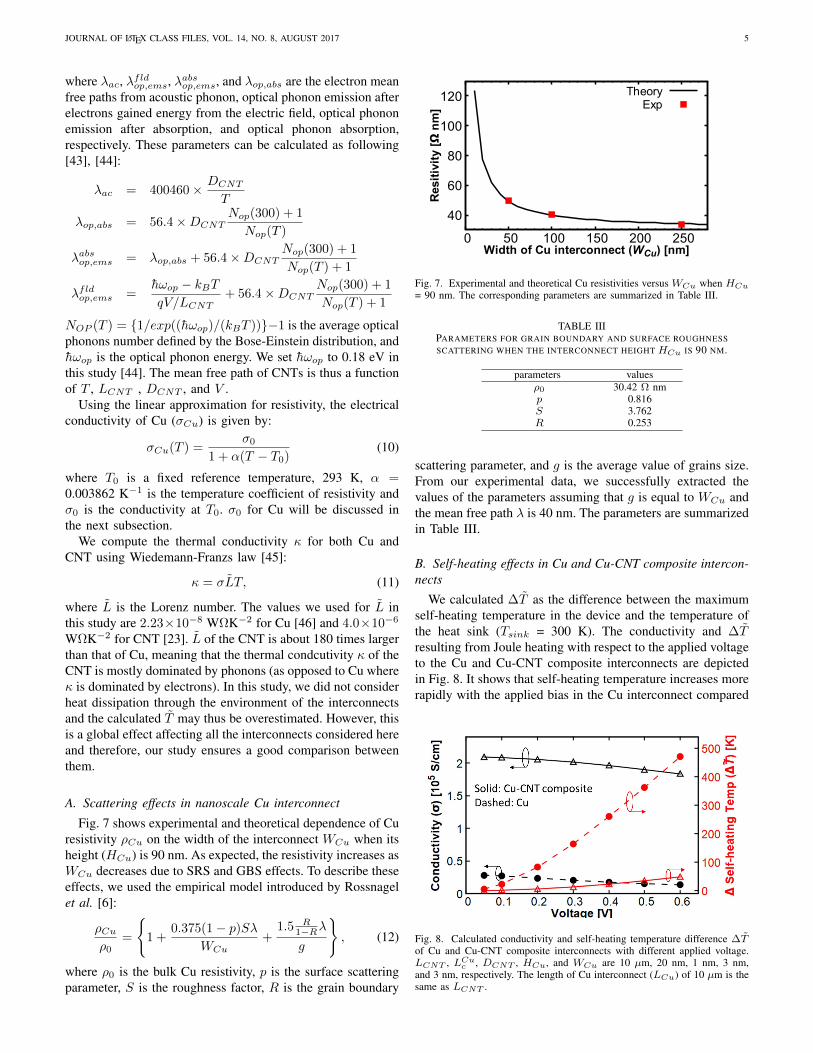
Fig. 7 shows experimental and theoretical dependence of Curesistivity ρCu on the width of the interconnect WCu when itsheight (HCu) is 90 nm. As expected, the resistivity increases asWCu decreases due to SRS and GBS effects. To describe theseeffects, we used the empirical model introduced by Rossnagelet al. [6]:
ρCu
ρ0=
1 +
0.375(1− p)SλWCu
+1.5 R
1−Rλ
g
, (12)
where ρ0 is the bulk Cu resistivity, p is the surface scatteringparameter, S is the roughness factor, R is the grain boundary
40
60
80
100
120
0 50 100 150 200 250
Res
itiv
ity
[Ω n
m]
Width of Cu interconnect (WCu) [nm]
TheoryExp
Fig. 7. Experimental and theoretical Cu resistivities versus WCu when HCu
= 90 nm. The corresponding parameters are summarized in Table III.
TABLE IIIPARAMETERS FOR GRAIN BOUNDARY AND SURFACE ROUGHNESSSCATTERING WHEN THE INTERCONNECT HEIGHT HCu IS 90 NM.
parameters valuesρ0 30.42 Ω nmp 0.816S 3.762R 0.253
scattering parameter, and g is the average value of grains size.From our experimental data, we successfully extracted thevalues of the parameters assuming that g is equal to WCu andthe mean free path λ is 40 nm. The parameters are summarizedin Table III.
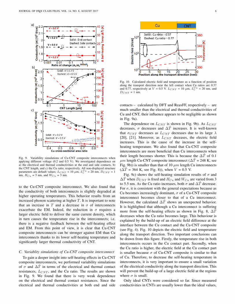
B. Self-heating effects in Cu and Cu-CNT composite intercon-nects
We calculated ∆T as the difference between the maximumself-heating temperature in the device and the temperature ofthe heat sink (Tsink = 300 K). The conductivity and ∆Tresulting from Joule heating with respect to the applied voltageto the Cu and Cu-CNT composite interconnects are depictedin Fig. 8. It shows that self-heating temperature increases morerapidly with the applied bias in the Cu interconnect compared
Fig. 8. Calculated conductivity and self-heating temperature difference ∆Tof Cu and Cu-CNT composite interconnects with different applied voltage.LCNT , LCu
c , DCNT , HCu, and WCu are 10 µm, 20 nm, 1 nm, 3 nm,and 3 nm, respectively. The length of Cu interconnect (LCu) of 10 µm is thesame as LCNT .
JOURNAL OF LATEX CLASS FILES, VOL. 14, NO. 8, AUGUST 2017 6
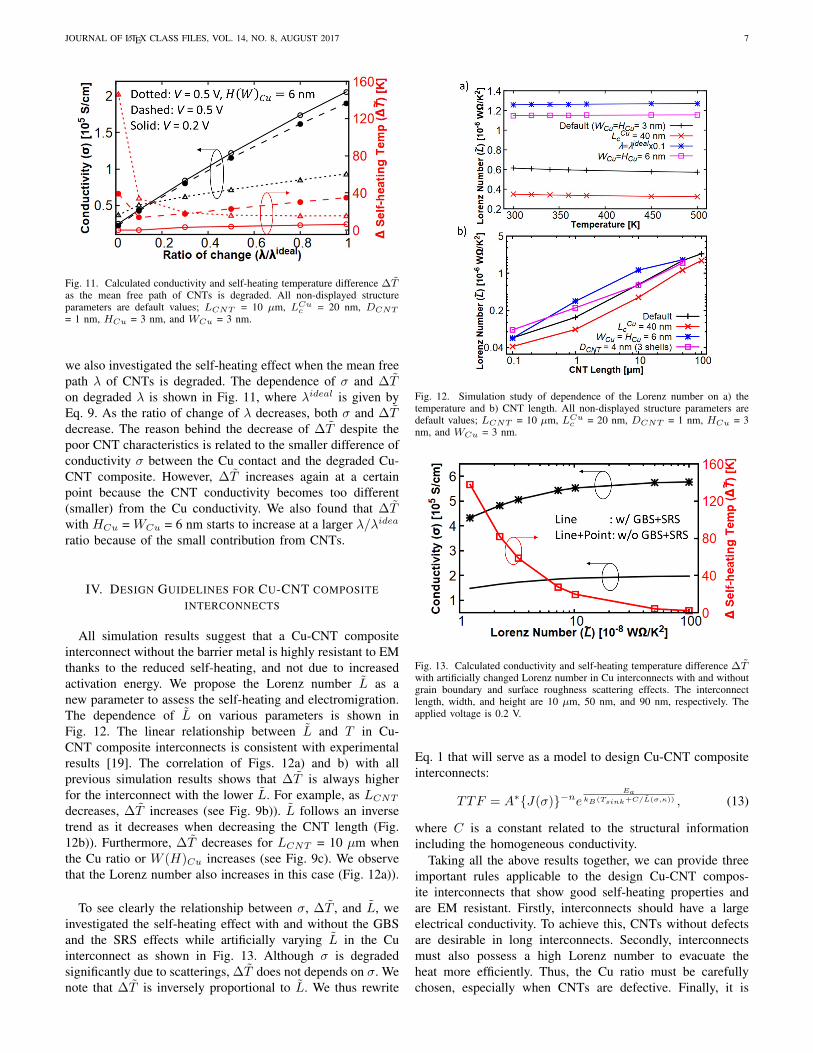
Fig. 9. Variability simulations of Cu-CNT composite interconnects whenapplying different voltage (0.2 and 0.5 V). We investigated dependence ona) the electrical and thermal conductivities at the end and side contacts, b)the CNT length, and c) the Cu ratio, respectively. All non-displayed structureparameters are default values; LCNT = 10 µm, LCu
c = 20 nm, DCNT = 1nm, HCu = 3 nm, and WCu = 3 nm.
to the Cu-CNT composite interconnect. We also found thatthe conductivity of both interconnects is slightly degraded athigher operating temperatures. This behavior results from anincreased phonon scattering at higher T . It is important to notethat an increase in T and a decrease in σ of interconnectsexacerbate the EM. Indeed, the reduction in σ requires alarger electric field to deliver the same current density, whichin turn causes the temperature rise in the interconnects; i.e.there is a negative feedback between the self-heating effectand EM. From this point of view, it is clear that Cu-CNTcomposite interconnects can be stronger against EM than Cuinterconnects thanks to its lower self-heating temperature andsignificantly larger thermal conductivity of CNT.
C. Variablity simulations of Cu-CNT composite interconnect
To gain a deeper insight into self-heating effects in Cu-CNTcomposite interconnects, we performed variability simulationsof σ and ∆T in terms of the electrical and thermal contactresistances, LCNT , and the Cu ratio. The results are shownin Fig. 9. We found that there is very weak dependenceon the electrical and thermal contact resistances. Since theelectrical and thermal conductivities at both end and side
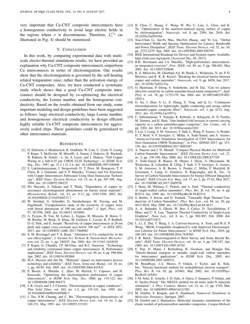
Fig. 10. Calculated electric field and temperature as a function of positionalong the transport direction near the left contact when Cu ratios are 0.37and 0.77, respectively at V = 0.5 V. LCNT = 10 µm, LCu
c = 20 nm, andDCNT = 1 nm.
contacts – calculated by DFT and ReaxFF, respectively – aremuch smaller than the electrical and thermal conductivities ofCu and CNT, their influence appears to be negligible as shownin Fig. 9a).
The dependence on LCNT is shown in Fig. 9b). As LCNT
decreases, σ decreases and ∆T increases. It is well-knownthat σCNT decreases as LCNT decreases due to its large λ[20], [21]. Moreover, as LCNT deceases, the electric fieldincreases. This is the cause of the increase in the self-heating temperature. We also found that Cu-CNT compositeinterconnects are more beneficial than Cu interconnects whentheir length becomes shorter. This is because the ∆T of 0.1µm length Cu-CNT composite interconnect (∆T = 248 K, seeFig. 9b)) is smaller than that of 10 µm length Cu interconnects(∆T = 364 K, see Fig. 8)), when V = 0.5 V.
Fig. 9c) shows the self-heating simulation results of σ and∆T when DCNT is fixed and HCu and WCu are varied from 3to 5.5 nm. As the Cu ratio increases, both σ and ∆T decrease.For σ, it is consistent with the general expectations because asCu becomes increasingly dominant, σ of a Cu-CNT compositeinterconnect becomes closer to that of a Cu interconnect.However, the calculated ∆T shows an unexpected behavior.It is highlighted that although a Cu interconnect is sufferingmore from the self-heating effects as shown in Fig. 8, ∆Tdecreases when the Cu ratio becomes large. This behaviour isexplained by the build-up of an electric field difference at theinterface between the Cu contact and the Cu-CNT composite(see Fig. 4). Fig. 10 depicts the electric field and temperaturealong the transport direction. Two important conclusions canbe drawn from this figure. Firstly, the temperature rise in bothinterconnects occurs in the Cu contact part. Secondly, whenthe Cu ratio is higher, the electric field at the Cu contact partis smaller because σ of Cu-CNT composite is similar to thatof Cu. Therefore, to decrease the self-heating temperature ininterconnects, it is very important to ensure a small variationof the electrical conductivity along the transport direction. Thiswill prevent the build-up of a large electric field at the regionswhere σ is small.
Only ideal CNTs were considered so far. Since measuredconductivities in CNTs are usually lower than the ideal values,
JOURNAL OF LATEX CLASS FILES, VOL. 14, NO. 8, AUGUST 2017 7
Fig. 11. Calculated conductivity and self-heating temperature difference ∆Tas the mean free path of CNTs is degraded. All non-displayed structureparameters are default values; LCNT = 10 µm, LCu
c = 20 nm, DCNT
= 1 nm, HCu = 3 nm, and WCu = 3 nm.
we also investigated the self-heating effect when the mean freepath λ of CNTs is degraded. The dependence of σ and ∆Ton degraded λ is shown in Fig. 11, where λideal is given byEq. 9. As the ratio of change of λ decreases, both σ and ∆Tdecrease. The reason behind the decrease of ∆T despite thepoor CNT characteristics is related to the smaller difference ofconductivity σ between the Cu contact and the degraded Cu-CNT composite. However, ∆T increases again at a certainpoint because the CNT conductivity becomes too different(smaller) from the Cu conductivity. We also found that ∆Twith HCu = WCu = 6 nm starts to increase at a larger λ/λidea
ratio because of the small contribution from CNTs.
IV. DESIGN GUIDELINES FOR CU-CNT COMPOSITEINTERCONNECTS
All simulation results suggest that a Cu-CNT compositeinterconnect without the barrier metal is highly resistant to EMthanks to the reduced self-heating, and not due to increasedactivation energy. We propose the Lorenz number L as anew parameter to assess the self-heating and electromigration.The dependence of L on various parameters is shown inFig. 12. The linear relationship between L and T in Cu-CNT composite interconnects is consistent with experimentalresults [19]. The correlation of Figs. 12a) and b) with allprevious simulation results shows that ∆T is always higherfor the interconnect with the lower L. For example, as LCNT
decreases, ∆T increases (see Fig. 9b)). L follows an inversetrend as it decreases when decreasing the CNT length (Fig.12b)). Furthermore, ∆T decreases for LCNT = 10 µm whenthe Cu ratio or W (H)Cu increases (see Fig. 9c). We observethat the Lorenz number also increases in this case (Fig. 12a)).
To see clearly the relationship between σ, ∆T , and L, weinvestigated the self-heating effect with and without the GBSand the SRS effects while artificially varying L in the Cuinterconnect as shown in Fig. 13. Although σ is degradedsignificantly due to scatterings, ∆T does not depends on σ. Wenote that ∆T is inversely proportional to L. We thus rewrite
Fig. 12. Simulation study of dependence of the Lorenz number on a) thetemperature and b) CNT length. All non-displayed structure parameters aredefault values; LCNT = 10 µm, LCu
c = 20 nm, DCNT = 1 nm, HCu = 3nm, and WCu = 3 nm.
Fig. 13. Calculated conductivity and self-heating temperature difference ∆Twith artificially changed Lorenz number in Cu interconnects with and withoutgrain boundary and surface roughness scattering effects. The interconnectlength, width, and height are 10 µm, 50 nm, and 90 nm, respectively. Theapplied voltage is 0.2 V.
Eq. 1 that will serve as a model to design Cu-CNT compositeinterconnects:
TTF = A∗J(σ)−neEa
kB(Tsink+C/L(σ,κ)) , (13)
where C is a constant related to the structural informationincluding the homogeneous conductivity.
Taking all the above results together, we can provide threeimportant rules applicable to the design Cu-CNT compos-ite interconnects that show good self-heating properties andare EM resistant. Firstly, interconnects should have a largeelectrical conductivity. To achieve this, CNTs without defectsare desirable in long interconnects. Secondly, interconnectsmust also possess a high Lorenz number to evacuate theheat more efficiently. Thus, the Cu ratio must be carefullychosen, especially when CNTs are defective. Finally, it is
JOURNAL OF LATEX CLASS FILES, VOL. 14, NO. 8, AUGUST 2017 8
very important that Cu-CNT composite interconnects havea homogenous conductivity to avoid large electric fields inthe regions where σ is discontinuous. Therefore, LCu
c (asillustrated in Fig. 4) should be minimized.
V. CONCLUSION
In this work, by comparing experimental data with multi-scale electro-thermal simulations results, we have provided anexplanation why Cu-CNT composite interconnects outperformCu interconnects in terms of electromigration. Our resultsshow that the electromigration is governed by the self-heatingrelated temparature raise, rather than the activation energy ofCu-CNT composites. Also, we have conducted a systematicstudy which shows that a good Cu-CNT composite inter-connect should be designed by co-optimizing the electricalconductivity, the Lorenz number, and the homogenous con-ductivity. Based on the results obtained from our study, someimportant modeling and design guidelines have been suggestedas follows: large electrical conductivity, large Lorenz number,and homogeneous electrical conductivity to design efficienthighly reliable Cu-CNT composite interconnects for aggres-sively scaled chips. These guidelines could be generalized toother interconnect materials.
REFERENCES
[1] D. Edelstein, J. Heidenreich, R. Goldblatt, W. Cote, C. Uzoh, N. Lustig,P. Roper, T. McDevittt, W. Motsifft, A. Simon, J. Dukovic, R. Wachnik,H. Rathore, R. Schulz , L. Su, S. Lucet, and J. Slattery, ”Full CopperWiring in a Sub-0.25 pm CMOS ULSI Technology”, in IEDM Tech.Dig., Dec. 1997, pp. 31.3.1-31.3.4. doi: 10.1109/IEDM.1997.650496
[2] S. Lakshminarayanan, J. Steigerwald, D. T. Price, M. Bourgeois, T. P.Chow, R. J. Gutmann, and S. P. Murarka, ”Contact and Via Structureswith Copper Interconnects Fabricated Using Dual Damascene Technol-ogy”, IEEE Trans. Electron Devices, vol. 15, no. 8, pp. 307-309, Aug.1994. doi: 10.1109/55.296225
[3] M.i Hayashi, S. Nakano and T. Wada, ”Dependence of copper in-terconnect electromigration phenomenon on barrier metal materials”,Microelectron. Reliab., vol. 43, no. 9-11, pp. 1545-1550, 2003. doi:10.1016/S0026-2714(03)00273-7
[4] W. Steinhgl, G. Schindler, G. Steinlesberger, M. Traving, and M.Engelhardt, ”Comprehensive study of the resistivity of copper wireswith lateral dimensions of 100 nm and smaller”, J. Appl. Phys., vol.97, 023706, 2005. doi: 10.1063/1.1834982
[5] A. Pyzyna, H. Tsai, M. Lofaro, L. Gignac, H. Miyazoe, R. Bruce, C.M. Breslin, M. Brink, D. Klaus, M. Guillorn, C. Lavoie, K. P. Rodbell,D.-G. Park, and E. Joseph, ”Resistivity of copper interconnects at 28 nmpitch and copper cross-sectional area below 100 nm2”, in IEEE IITC,2017, doi: 10.1109/IITC-AMC.2017.7968982
[6] S. M. Rossnagel and T. S. Kuan, ”Alteration of Cu conductivity in thesize effect regime”, J. Vacuum Sci. Technol. B, Nanotechnol. Microelec-tron.,vol. 22, no. 1, pp. 240247, Jan. 2004. doi: 10.1116/1.1642639
[7] P. Kapur, G. Chandra, J.P. McVittie, and K.C. Saraswat, ”Technologyand reliability constrained future copper interconnects. II. Performanceimplications”, IEEE Trans. Electron Devices, vol. 49, no. 4, pp. 598-604,Apr. 2002. doi: 10.1109/16.992868
[8] M.A. Hussein and Jun He, ”Materials’ impact on interconnect processtechnology and reliability”, IEEE Trans. Semicond. Manuf., vol. 18, no.1, pp. 69-85, Feb. 2005. doi: 10.1109/TSM.2004.841832
[9] P. Besser, A. Marathe, L. Zhao, M. Herrick, C. Capasso, and H.Kawasaki, ”Optimizing the electromigration performance of copperinterconnects”, in IEDM Tech. Dig., Dec. 2000, pp. 119-122. doi:10.1109/IEDM.2000.904272
[10] J. R. Lloyd, and J. J. Clement, ”Electromigration in copper conductors”,Thin Solid Films, vol. 262, no. 1-2, pp. 135-141, Jun. 1995. doi:10.1016/0040-6090(94)05806-7
[11] J. Tao, N.W. Cheung, and C. Hu, ”Electromigration characteristics ofcopper interconnects”, IEEE Electron Device Lett., vol. 14, no. 5, pp.249-251, May 1993. doi: 10.1109/55.215183
[12] H. Chen, C. Huang, C. Wang, W. Wu, C. Liao, L. Chen, and K.Tu, ”Optimization of the nanotwin-induced zigzag surface of copperby electromigration”, Nanoscale, vol. 8, pp. 2584, Jan. 2016. doi:10.1039/c5nr05418d
[13] Xiao-Chun Li, Jun-Fa Mao, Hui-Fen Huang, and Ye Liu, ”GlobalInterconnect Width and Spacing Optimization for Latency, Bandwidthand Power Dissipation”, IEEE Trans. Electron Devices, vol. 52, no. 10,pp. 2272-2279, Sep. 2005. doi: 10.1109/TED.2005.856795
[14] IEEE International Roadmap for Devices and Systems report. Available:https://irds.ieee.org/reports [Accessed Dec. 04, 2017].
[15] R.H. Havemann and J.A. Hutchby, ”High-performance interconnects:an integration overview”, Proc. IEEE, vol. 89, no. 5, pp. 586-601, May2001. doi: 10.1109/5.929646
[16] K. Z. Milowska, M. Ghorbani-Asl, M. Burda, L. Wolanicka, N. ati, P. D.Bristowe, and K. K. K. Koziol, ”Breaking the electrical barrier betweencopper and carbon nanotubes”, Nanoscale, vol. 9, pp. 8458, Jun. 2017.doi: 10.1039/c7nr02142a
[17] O. Hjortstam, P. Isberg, S. Soderholm, and H. Dai, ”Can we achieveultra-low resistivity in carbon nanotube-based metal composites?”, Appl.Phys. A, vol. 78, pp. 11751179, Jan. 2004. doi: 10.1007/s00339-003-2424-x
[18] G. Xu, J. Zhao, S. Li, X. Zhang, Z. Yong, and Q. Li, ”Continuouselectrodeposition for lightweight, highly conducting and strong carbonnanotube-copper composite fibers”, Nanoscale, vol. 3, pp. 4215, Aug.2011. doi: 10.1039/c1nr10571j
[19] C. Subramaniam, T. Yamada, K. Kobashi, A. Sekiguchi, D. N. Futaba,M. Yumura, and K. Hata, ”One hundred fold increase in current carryingcapacity in a carbon nanotubecopper composite”, Nat. Comm., vol. 4,pp. 2202, Jul. 2013. doi: 10.1038/ncomms3202
[20] J. Lee, J. Liang, S. M. Amoroso, T. Sadi, L. Wang, P. Asenov, A. Pender,D. T. Reid, V. P. Georgiev, C. Millar, A. Todri-Sanial, and A. Asenov,”Atoms-to-Circuits Simulation Investigation of CNT Interconnects forNext Generation CMOS Technology”, in Proc. SISPAD 2017, pp. 153-156. doi: 10.23919/SISPAD.2017.8085287
[21] A. Naeemi and J. D. Meindl, ”Compact Physical Models for MultiwallCarbon-Nanotube Interconnects”, IEEE Electron Device Lett., vol. 27,no. 5, pp. 338-340, May 2006. doi: 10.1109/LED.2006.873765
[22] A. Todri-Sanial, R. Ramos, H. Okuno, J. Dijon, A. Dhavamani, M.Wislicenus, K. Lilienthal, B. Uhlig, T. Sadi, V. P. Georigev, A. Asenov,S. M. Amoroso, A. R. Brown, A. Pender, C. Millar, F. Motzfeld, B.Gotsmann, J. Liang, G. Gonalves, N. Rupesinghe, and K. Teo, ”ASurvey of Carbon Nanotube Interconnects for Energy Efficient IntegratedCircuits”, IEEE Circuits Syst. Mag., vol. 17, no. 2, pp. 47-62, May 2017.doi: 10.1109/MCAS.2017.2689538
[23] J. Hone, M. Whitney, C. Piskoti, and A. Zettl, ”Thermal conductivityof single-walled carbon nanotubes”, Phys. Rev. B, vol. 59, no. 4, pp.R2514, Jan. 1999. doi: 10.1103/PhysRevB.59.R2514
[24] S. Berber, Y. Kwon, and D. Tomnek, ”Unusually High Thermal Con-ductivity of Carbon Nanotubes”, Phys. Rev. Lett., vol. 84, no. 20, pp.4613-4616, May 2000. doi: 10.1103/PhysRevLett.84.4613
[25] A. A. Balandin, S. Ghosh, W. Bao, I. Calizo, D. Teweldebrhan, F.Miao, and C. N. Lau, ”Superior Thermal Conductivity of Single-LayerGraphene”, Nano Lett., vol. 8, no. 3, pp. 902-907, Feb. 2008. doi:10.1021/nl0731872
[26] L. Li, Z. Zhu, T. Wang, J. A. Currivan-Incorvia, A. Yoon, and H.-S. P.Wong, ”BEOL Compatible Graphene/Cu with Improved Electromigra-tion Lifetime for Future Interconnects”, in IEDM Tech. Dig., 2016, pp.240-243. doi: 10.1109/IEDM.2016.7838383
[27] J. R. Balck, ”Electromigration-A Brief Survey and Some Recent Re-sults”, IEEE Trans. Electron Devices, vol. 16, no. 4, pp. 338-347, Apr.1969. doi: 10.1109/T-ED.1969.16754
[28] E. Pop, D. Mann, J. Reifenberg, K. Goodson, and Hongjie Dai,”Electro-thermal transport in metallic single-wall carbon nanotubesfor interconnect applications”, in IEDM Tech. Dig., 2005. doi:10.1109/IEDM.2005.1609321
[29] M. Brandbyge, J.-L. Mozos, P. Ordejn, J. Taylor, and K. Stok-bro, ”Density-functional method for noneqilibrium electron transport”,Phys. Rev. B, vol. 65, pp. 165401, Mar. 2002. doi: 10.1103/Phys-RevB.65.165401
[30] J. M. Soler, E. Artacho, J. D. Gale, A. Garca, J. Junquera, P. Ordejn, andD. Snchez-Portal,” The SIESTA method for ab initio order-N materialssimulation”, J. Phys. Condens. Matter, vol. 14, no. 11, pp. 2745, Mar.2002. doi: 10.1088/0953-8984/14/11/302
[31] M. Griebel, S. Knapek, and G. Zumbusch, Numerical Simulation inMolecular Dynamics, Springer, 2007.
[32] M. Griebel and J. Hamaekers, Molecular dynamics simulations of theelastic moduli of polymercarbon nanotube composites, Comput.Methods
JOURNAL OF LATEX CLASS FILES, VOL. 14, NO. 8, AUGUST 2017 9
in Appl.Mech.Eng., vol. 193, no. 17-20, pp. 1773-1788, May 2004. doi:10.1016/j.cma.2003.12.025
[33] K. D. Nielson, A. C. T. van Duin, J. Oxgaard, W. Deng, and W. A.Goddard, ”Development of the ReaxFF reactive force field for describingtransition metal catalyzed reactions, with application to the initial stagesof the catalytic formation of carbon nanotubes”, J. Phys. Chem. A., vol.109, pp. 493-499, Dec. 2005. doi: 10.1021/jp046244d
[34] Atomistix ToolKit version 2016.4, QuantumWise A/S. Available:http://www.quantumwise.com [Accessed Dec. 04, 2017].
[35] J. P. Perdew, K. Burke, and M. Ernzerhof, ”Generalized GradientApproximation Made Simple”, Phys. Rev. Lett., vol. 77, pp. 3865, Oct.1996. doi: 10.1103/PhysRevLett.77.3865
[36] S. Grimme, J. Antony, S. Ehrlich, and H. Krieg, ”A consistent andaccurate ab initio parametrization of density functional dispersion cor-rection (DFT-D) for the 94 elements H-Pu”, J. Chem. Phys., vol. 132,pp. 154104, Apr. 2010. doi:10.1063/1.3382344.
[37] P. Avouris, Z. Chen, and V. Perebeinos, ”Carbon-based electronics”, Nat.Nanotech., vol. 2, pp. 605615, Sep. 2007. doi: 10.1038/nnano.2007.300
[38] A. D. Franklin and Z. Chen, ”Length scaling of carbon nanotubetransistors”, Nat. Nanotech., vol. 5, pp. 858-862, Dec. 2010. doi:10.1038/NNANO.2010.220
[39] Jianshi Tang, Qing Cao, Damon B. Farmer, George Tulevski, and Shu-Jen Han, ”Carbon nanotube complementary logic with low-temperatureprocessed end-bonded metal contacts”, in IEDM Tech. Dig., 2016. doi:10.1109/IEDM.2016.7838350
[40] Qing Cao, Shu-Jen Han, Jerry Tersoff, Aaron D. Franklin, Yu Zhu,Zhen Zhang, George S. Tulevski, Jianshi Tang, and Wilfried Haensch,”End-bonded contacts for carbon nanotube transistors with low, size-independent resistance”, Science, vol. 350, no. 6256, pp. 68-72, Oct.2015. doi: 10.1126/science.aac8006
[41] Juekuan Yang, Yang Yang, Scott W. Waltermire, Timothy Gutu, AlfredA. Zinn, Terry T. Xu, Yunfei Chen, and Deyu Li, ”Measurement of theIntrinsic Thermal Conductivity of a Multiwalled Carbon Nanotube andIts Contact Thermal Resistance with the Substrate”, Small, vol. 7, no.16, pp. 2334-2340, Jun. 2011. doi: 10.1002/smll.201100429
[42] Baratunde A. Cola, Xianfan Xu, and Timothy S. Fisher, ”Increased realcontact in thermal interfaces: A carbon nanotube/foil material”, Appl.Phys. Lett., vol. 90, pp. 093513, Mar. 2007. doi: 10.1063/1.2644018
[43] K. M. Mohsin, A. Srivastava, A. K. Sharma, and C. Mayberry, ”Char-acterization of MWCNT VLSI Interconnect with Self-heating InducedScatterings”, in Proc. IEEE Comput. Soc. Annu. Symp. VLSI, 2014, pp.368373. doi: 10.1109/ISVLSI.2014.31
[44] E. Pop, D. A. Mann, K. E. Goodson, and H. Dai, ”Electrical andthermal transport in metallic single-wall carbon nanotubes on insulatingsubstrates”, J. Appl. Phys., vol. 101, no. 9, pp. 093710, May 2007. doi:10.1063/1.2717855
[45] M. Jonson, and G. D. Mahan, ”Mott’s formula for the thermopower andthe Wiedemann-Franz law”, Phys. Rev. B., vol. 21, no. 10, pp. 4223-4229, May 1980. doi: 10.1103/PhysRevB.21.4223
[46] Kittel, C., Introduction to Solid State Physics., John Wiley and Sons,2005.