Embed Size (px)
Citation preview
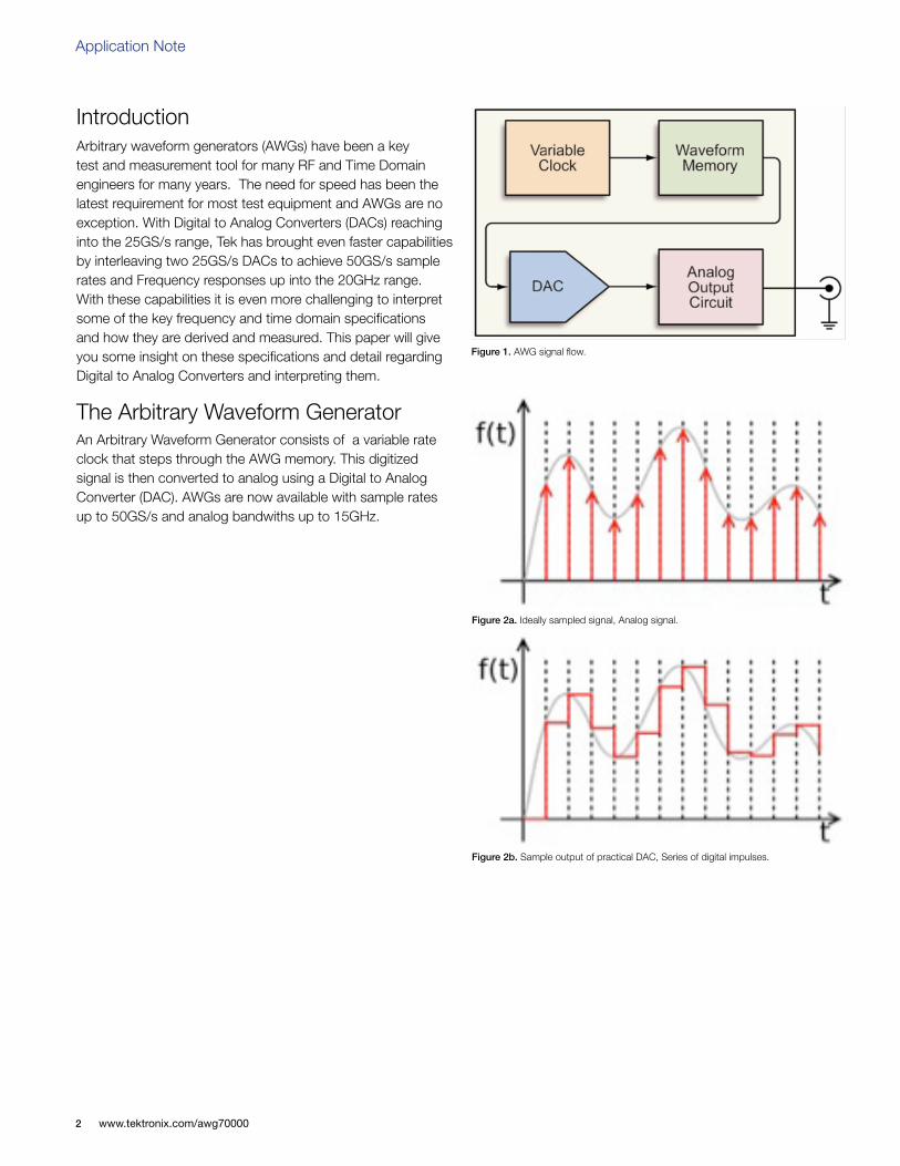
Understanding AWG70000A Series Frequency Response and DAC Performance Application Note
What you will learn:
You will gain an understanding of the AWG frequency response characteristics and time domain specifications, plus DAC details and how to interpret them.
Application Note
www.tektronix.com/awg700002
IntroductionArbitrary waveform generators (AWGs) have been a key test and measurement tool for many RF and Time Domain engineers for many years. The need for speed has been the latest requirement for most test equipment and AWGs are no exception. With Digital to Analog Converters (DACs) reaching into the 25GS/s range, Tek has brought even faster capabilities by interleaving two 25GS/s DACs to achieve 50GS/s sample rates and Frequency responses up into the 20GHz range. With these capabilities it is even more challenging to interpret some of the key frequency and time domain specifications and how they are derived and measured. This paper will give you some insight on these specifications and detail regarding Digital to Analog Converters and interpreting them.
The Arbitrary Waveform GeneratorAn Arbitrary Waveform Generator consists of a variable rate clock that steps through the AWG memory. This digitized signal is then converted to analog using a Digital to Analog Converter (DAC). AWGs are now available with sample rates up to 50GS/s and analog bandwiths up to 15GHz.
Figure 1. AWG signal flow.
Figure 2a. Ideally sampled signal, Analog signal.
Figure 2b. Sample output of practical DAC, Series of digital impulses.
www.tektronix.com/awg70000 3
Understanding AWG70000A Series Frequency Response and DAC Performance
Considerations
In order to produce the best quality signals, following the Nyquist formula is required. The sampling frequency must be at least twice the expected output frequency. The more oversampling that can be done will reduce the step effect or the "zero order hold" characteristic of sampling. These zero order hold effects can cause multiple unwanted harmonics above f the Nyquist frequency. It also introduces quantization errors adding to the low level noise. See Figure 2a and 2b.
Typical AWG DAC specifications
Sample rate
- The master clock rate of the system (fixed or variable) Example: AWG70K = 1.5KS/s – 50GS/s
Resolution/ Dynamic Range
- The digital resolution of the output, typically in terms of “bits” Example: AWG70K - 10 bits
Effective Number Of Bits (ENOB)
- ENOB is a measure of how effective is the DAC. It specifies the number of usable bits above the noise floor. If a DAC is able to represent signal levels below the noise floor, the lower bits only represent system noise and do not contain useful information. ENOB will change depending on the carrier frequency and in some cases is very hard to measure.
Signal to Noise (S/N) Ratio
The often quoted figure of merit is:
- S/N = (Bits * 6.02 +1.76) dB
- For 10 bits this is 61.78 dB
This is not the noise floor (noise density). It is the integrated RMS noise up to the Nyquist frequency.
- But what is forgotten or misunderstood, is that the noise term in this equation is the total noise power over the full Nyquist band. The spectral noise density, or in other words the noise in each small frequency increment, is much lower, closer to -70 dB or less. So when you look on a spectrum analyzer with a narrow Resolution Bandwidth, the noise floor you see is just the noise in the RBW. To get a signal to noise ratio you would integrate the noise power over the appropriate bandwidth. For instance, integrating over 1 GHz bandwidth rather than the 12.5 GHz Nyquist band you would reduce the noise by sqrt (12.5) = 3.54 or about 10 dB.
- The key factor is how much can you oversample. When you oversample you spread the quantization noise over a wider frequency band.
Application Note
www.tektronix.com/awg700004
Signal to Noise and Distortion (SINAD)
- Integrate all of the distortion spurs and thermal noise along with the quantization noise
Spurious-Free Dynamic Range (SFDR)
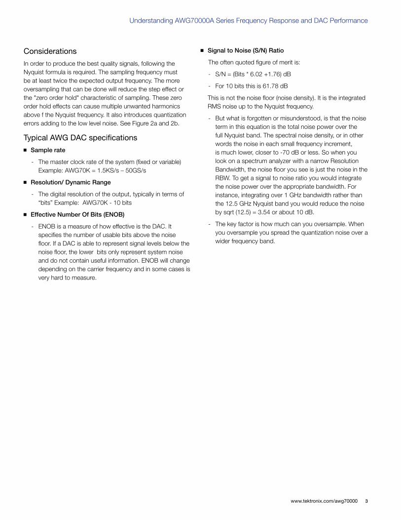
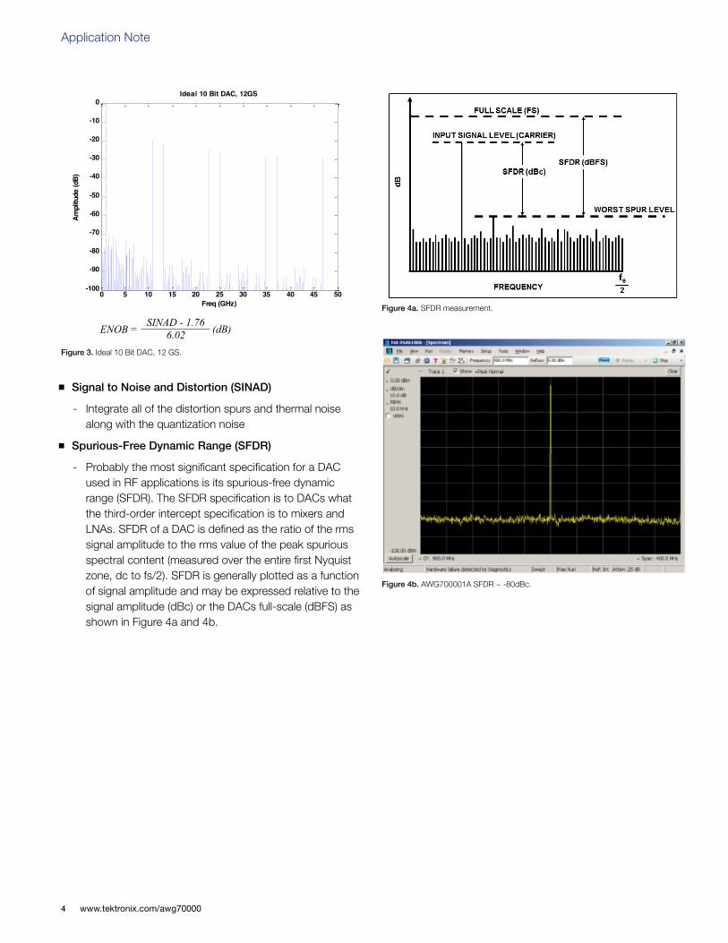
- Probably the most significant specification for a DAC used in RF applications is its spurious-free dynamic range (SFDR). The SFDR specification is to DACs what the third-order intercept specification is to mixers and LNAs. SFDR of a DAC is defined as the ratio of the rms signal amplitude to the rms value of the peak spurious spectral content (measured over the entire first Nyquist zone, dc to fs/2). SFDR is generally plotted as a function of signal amplitude and may be expressed relative to the signal amplitude (dBc) or the DACs full-scale (dBFS) as shown in Figure 4a and 4b.
0 5 10 15 20 25 30 35 40 45 50-100
-90
-80
-70
-60
-50
-40
-30
-20
-10
0
Ampl
itude
(dB)
Freq (GHz)
Ideal 10 Bit DAC, 12GS
ENOB = SINAD - 1.766.02 (dB)
Figure 3. Ideal 10 Bit DAC, 12 GS.
Figure 4b. AWG700001A SFDR ~ -80dBc.
Figure 4a. SFDR measurement.
www.tektronix.com/awg70000 5
Understanding AWG70000A Series Frequency Response and DAC Performance
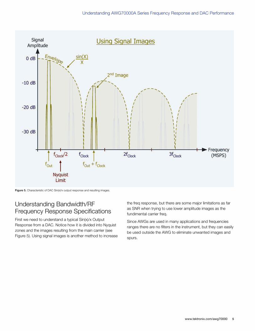
Understanding Bandwidth/RF Frequency Response SpecificationsFirst we need to understand a typical Sin(x)/x Output Response from a DAC. Notice how it is divided into Nyquist zones and the images resulting from the main carrier (see Figure 5). Using signal images is another method to increase
the freq response, but there are some major limitations as far as SNR when trying to use lower amplitude images as the fundimental carrier freq.
Since AWGs are used in many applications and frequencies ranges there are no filters in the instrument, but they can easily be used outside the AWG to eliminate unwanted images and spurs.
Figure 5. Characteristic of DAC Sin(x)/x output response and resulting images.
Application Note
www.tektronix.com/awg700006
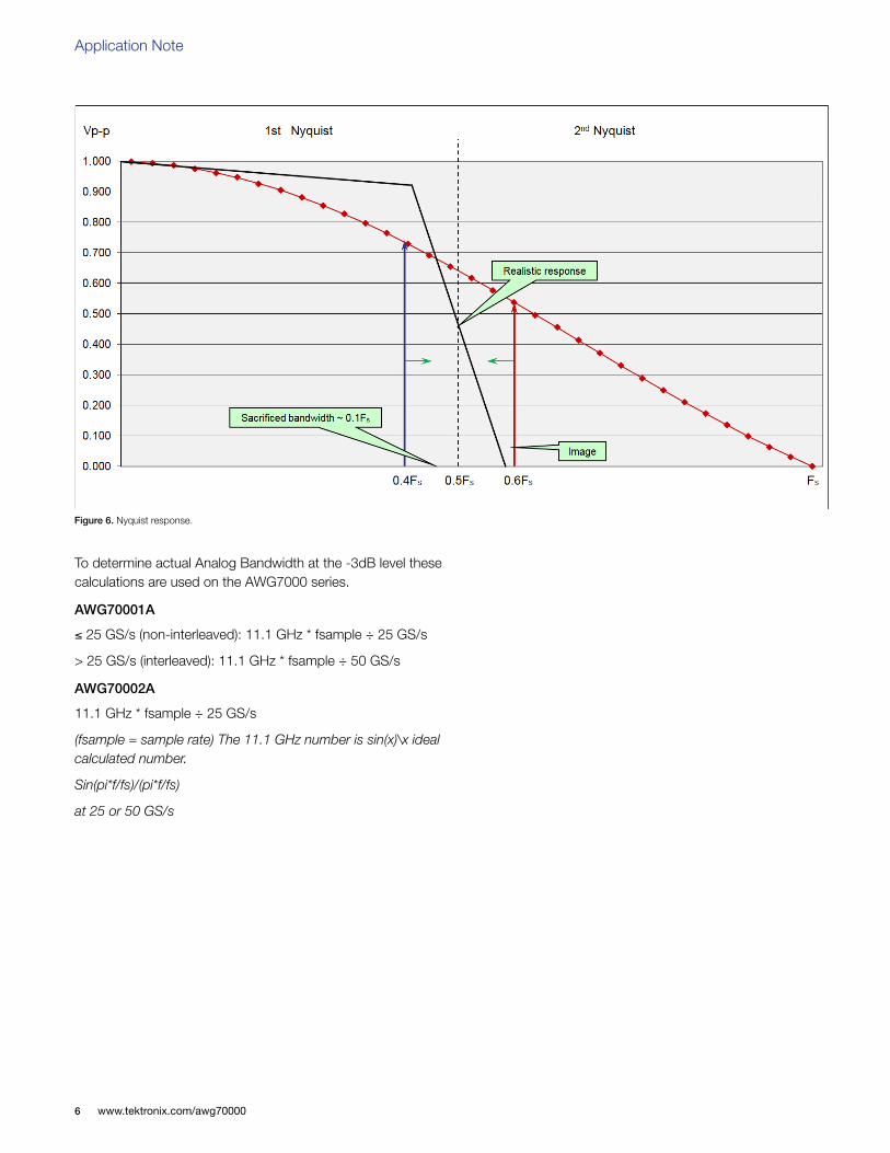
Figure 6. Nyquist response.
To determine actual Analog Bandwidth at the -3dB level these calculations are used on the AWG7000 series.
AWG70001A
≤ 25 GS/s (non-interleaved): 11.1 GHz * fsample ÷ 25 GS/s
> 25 GS/s (interleaved): 11.1 GHz * fsample ÷ 50 GS/s
AWG70002A
11.1 GHz * fsample ÷ 25 GS/s
(fsample = sample rate) The 11.1 GHz number is sin(x)\x ideal calculated number.
Sin(pi*f/fs)/(pi*f/fs)
at 25 or 50 GS/s
www.tektronix.com/awg70000 7
Understanding AWG70000A Series Frequency Response and DAC Performance
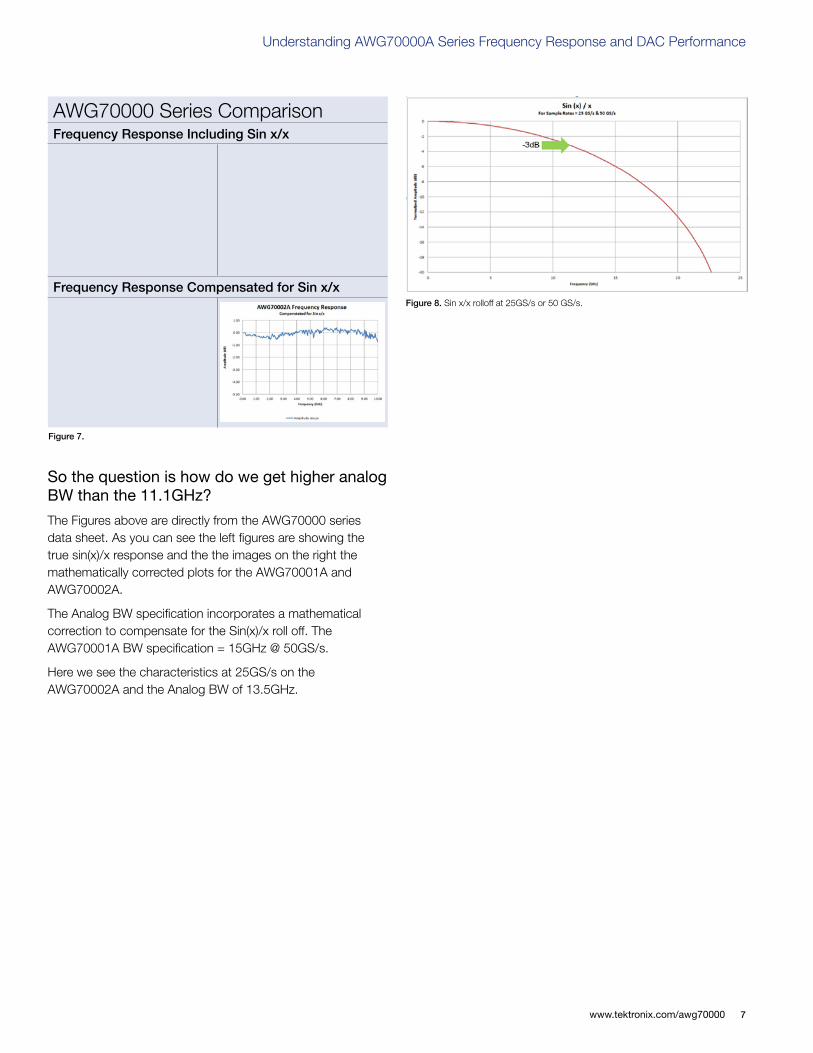
Figure 8. Sin x/x rolloff at 25GS/s or 50 GS/s.
Figure 7.
So the question is how do we get higher analog BW than the 11.1GHz?
The Figures above are directly from the AWG70000 series data sheet. As you can see the left figures are showing the true sin(x)/x response and the the images on the right the mathematically corrected plots for the AWG70001A and AWG70002A.
The Analog BW specification incorporates a mathematical correction to compensate for the Sin(x)/x roll off. The AWG70001A BW specification = 15GHz @ 50GS/s.
Here we see the characteristics at 25GS/s on the AWG70002A and the Analog BW of 13.5GHz.
AWG70000 Series ComparisonFrequency Response Including Sin x/x
Frequency Response Compensated for Sin x/x
Application Note
www.tektronix.com/awg700008
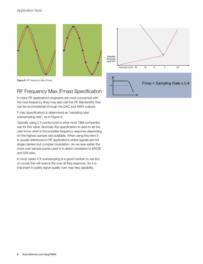
RF Frequency Max (Fmax) SpecificationIn many RF applications engineers are more concerned with the max frequency (they may also call this RF Bandwidth) that can be accomplished through the DAC and AWG outputs.
F max (specification) is determined as “sampling rate/ oversampling rate”, as in Figure 9.
Typically using 2.5 points/cycle is what most T&M companies use for this value. Normally this specification is used to let the user know what is the possible frequency response depending on the highest sample rate available. When using this term it is usually referenced in RF applications where signals are not single carriers but complex modulation. As we saw earlier the more over sample points used is in direct correlation to ENOB and S/N ratio.
In most cases 4 X oversampling is a good number to use but of course this will reduce the over all freq response. So it is important to justify signal quality over max freq capability.
Figure 9. RF Frequency Max (Fmax).
www.tektronix.com/awg70000 9
Understanding AWG70000A Series Frequency Response and DAC Performance
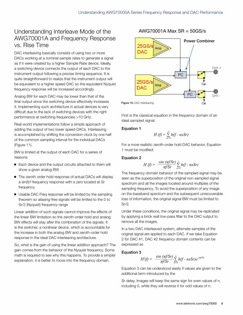
Understanding Interleave Mode of the AWG70001A and Frequency Response vs. Rise TimeDAC interleaving basically consists of using two or more DACs working at a nominal sample rates to generate a signal as if it were created by a higher Sample Rate device. Ideally, a switching device connects the output of each DAC to the instrument output following a precise timing sequence. It is quite straightforward to realize that the instrument output will be equivalent to a higher speed DAC so the equivalent Nyquist frequency response will be increased accordingly.
Analog BW for each DAC may be lower than that of the final output since the switching device effectively increases it. Implementing such architecture in actual devices is very difficult due to the lack of switching devices with the right performance at switching frequencies >10 GHz.
Real-world implementations follow a simple approach of adding the output of two lower speed DACs. Interleaving is accomplished by shifting the conversion clock by one half of the common sampling interval for the individual DACs (Figure 11).
BW is limited at the output of each DAC for a series of reasons:
Each device and the output circuits attached to them will show a given analog BW.
The zeroth order hold response of actual DACs will display a sin(f)/f frequency response with a zero located at Sr frequency.
Usable DAC Freq response will be limited by the sampling theorem so aliasing-free signals will be limited to the 0 to Sr/2 (Nyquist) frequency range
Linear addition of such signals cannot improve the effects of the linear BW limitation so the zeroth-order hold and analog BW effects will stay after the combination of the signals. It is the switcher, a nonlinear device, which is accountable for the increase in both the analog BW and zeroth-order hold response in the ideal DAC interleaving architecture.
So, what is the gain of using the linear addition approach? The gain comes from the behavior of the Nyquist frequency. Some math is required to see why this happens. To provide a simpler explanation, it is better to move into the frequency domain.
First is the classical equation in the frequency domain of an ideal sampled signal:
Equation 1
For a more realistic zeroth-order hold DAC behavior, Equation 1 must be modified:
Equation 2
The frequency-domain behavior of the sampled signal may be seen as the superposition of the original non-sampled signal spectrum and all the images located around multiples of the sampling frequency. To avoid the superposition of any image on the baseband spectrum and the subsequent unrecoverable loss of information, the original signal BW must be limited to Sr/2.
Under these conditions, the original signal may be replicated by applying a brick wall low-pass filter to the DAC output to remove all the images.
In a two DAC interleaved system, alternate samples of the original signal are applied to each DAC. If we take Equation 2 for DAC #1, DAC #2 frequency domain contents can be expressed as
Equation 3
Equation 3 can be understood easily if values are given to the additional term introduced by the
Sr delay. Images will keep the same sign for even values of n, including 0, while they will reverse it for odd values of n.
H (f) = ∑ h(f - nxSr)∞
n=0
H (f) = ∑ h(f - nxSr)∞
n=0
sin (πf/Sr)πf/Sr
H'(f) = ∑ h(f - nxSr)e∞
n=0
-jπf/Srsin (πf/Sr)πf/Sr
Figure 10. DAC Interleaving.
AWG70001A Max SR = 50GS/s
Power Combiner
Application Note
www.tektronix.com/awg7000010
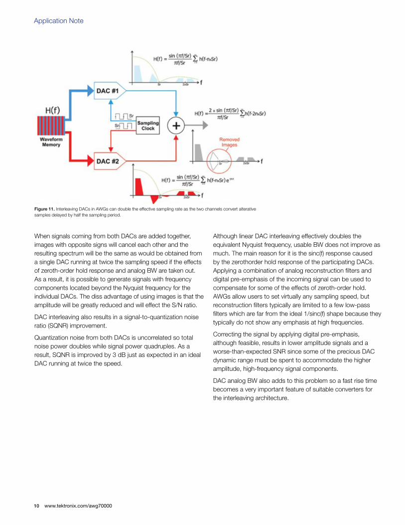
Figure 11. Interleaving DACs in AWGs can double the effective sampling rate as the two channels convert alterative samples delayed by half the sampling period.
When signals coming from both DACs are added together, images with opposite signs will cancel each other and the resulting spectrum will be the same as would be obtained from a single DAC running at twice the sampling speed if the effects of zeroth-order hold response and analog BW are taken out. As a result, it is possible to generate signals with frequency components located beyond the Nyquist frequency for the individual DACs. The diss advantage of using images is that the amplitude will be greatly reduced and will effect the S/N ratio.
DAC interleaving also results in a signal-to-quantization noise ratio (SQNR) improvement.
Quantization noise from both DACs is uncorrelated so total noise power doubles while signal power quadruples. As a result, SQNR is improved by 3 dB just as expected in an ideal DAC running at twice the speed.
Although linear DAC interleaving effectively doubles the equivalent Nyquist frequency, usable BW does not improve as much. The main reason for it is the sinc(f) response caused by the zerothorder hold response of the participating DACs. Applying a combination of analog reconstruction filters and digital pre-emphasis of the incoming signal can be used to compensate for some of the effects of zeroth-order hold. AWGs allow users to set virtually any sampling speed, but reconstruction filters typically are limited to a few low-pass filters which are far from the ideal 1/sinc(f) shape because they typically do not show any emphasis at high frequencies.
Correcting the signal by applying digital pre-emphasis, although feasible, results in lower amplitude signals and a worse-than-expected SNR since some of the precious DAC dynamic range must be spent to accommodate the higher amplitude, high-frequency signal components.
DAC analog BW also adds to this problem so a fast rise time becomes a very important feature of suitable converters for the interleaving architecture.
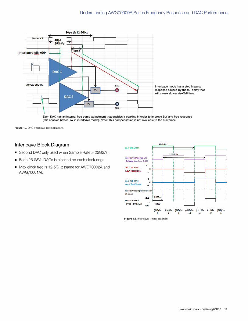
www.tektronix.com/awg70000 11
Understanding AWG70000A Series Frequency Response and DAC Performance
Figure 13. Interleave Timing diagram.
Interleave Block Diagram
Second DAC only used when Sample Rate > 25GS/s.
Each 25 GS/s DACs is clocked on each clock edge.
Max clock freq is 12.5GHz (same for AWG70002A and AWG70001A).
Figure 12. DAC Interleave block diagram.
Each DAC has an internal freq comp adjustment that enables a peaking in order to improve BW and freq response (this enables better BW in interleave mode). Note: This compensation is not available to the customer.
Interleave mode has a step in pulse response caused by the 90˚ delay that will cause slower rise/fall time.
Application Note
www.tektronix.com/awg7000012
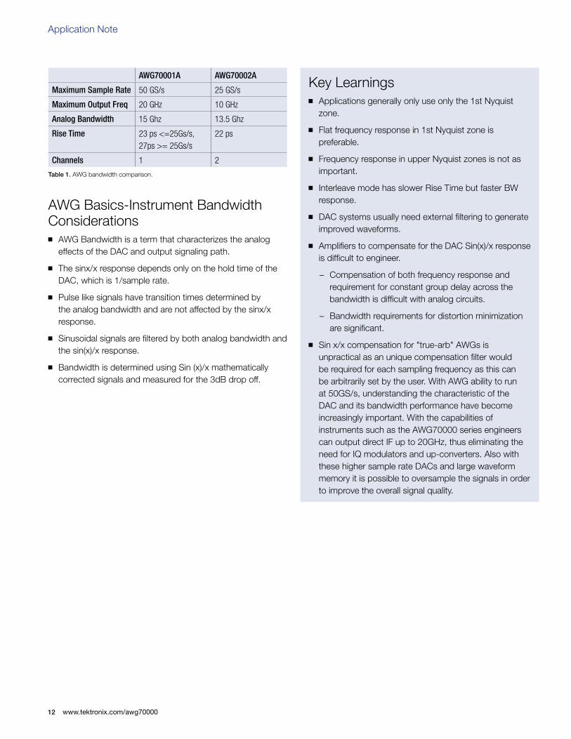
AWG Basics-Instrument Bandwidth Considerations AWG Bandwidth is a term that characterizes the analog
effects of the DAC and output signaling path.
The sinx/x response depends only on the hold time of the DAC, which is 1/sample rate.
Pulse like signals have transition times determined by the analog bandwidth and are not affected by the sinx/x response.
Sinusoidal signals are filtered by both analog bandwidth and the sin(x)/x response.
Bandwidth is determined using Sin (x)/x mathematically corrected signals and measured for the 3dB drop off.
Key Learnings Applications generally only use only the 1st Nyquist
zone.
Flat frequency response in 1st Nyquist zone is preferable.
Frequency response in upper Nyquist zones is not as important.
Interleave mode has slower Rise Time but faster BW response.
DAC systems usually need external filtering to generate improved waveforms.
Amplifiers to compensate for the DAC Sin(x)/x response is difficult to engineer.
– Compensation of both frequency response and requirement for constant group delay across the bandwidth is difficult with analog circuits.
– Bandwidth requirements for distortion minimization are significant.
Sin x/x compensation for "true-arb" AWGs is unpractical as an unique compensation filter would be required for each sampling frequency as this can be arbitrarily set by the user. With AWG ability to run at 50GS/s, understanding the characteristic of the DAC and its bandwidth performance have become increasingly important. With the capabilities of instruments such as the AWG70000 series engineers can output direct IF up to 20GHz, thus eliminating the need for IQ modulators and up-converters. Also with these higher sample rate DACs and large waveform memory it is possible to oversample the signals in order to improve the overall signal quality.
Table 1. AWG bandwidth comparison.
AWG70001A AWG70002A
Maximum Sample Rate 50 GS/s 25 GS/s
Maximum Output Freq 20 GHz 10 GHz
Analog Bandwidth 15 Ghz 13.5 Ghz
Rise Time 23 ps <=25Gs/s, 27ps >= 25Gs/s
22 ps
Channels 1 2

www.tektronix.com/awg70000 13
Understanding AWG70000A Series Frequency Response and DAC Performance
Contact Tektronix:ASEAN / Australia (65) 6356 3900
Austria* 00800 2255 4835Balkans, Israel, South Africa and other ISE Countries +41 52 675 3777
Belgium* 00800 2255 4835Brazil +55 (11) 3759 7627Canada 1 (800) 833-9200
Central East Europe and the Baltics +41 52 675 3777Central Europe & Greece +41 52 675 3777
Denmark +45 80 88 1401Finland +41 52 675 3777
France* 00800 2255 4835Germany* 00800 2255 4835
Hong Kong 400-820-5835Ireland* 00800 2255 4835
India +91-80-30792600Italy* 00800 2255 4835
Japan 0120-441-046Luxembourg +41 52 675 3777
Macau 400-820-5835Mongolia 400-820-5835
Mexico, Central/South America & Caribbean 52 (55) 56 04 50 90Middle East, Asia and North Africa +41 52 675 3777
The Netherlands* 00800 2255 4835Norway 800 16098
People’s Republic of China 400-820-5835Poland +41 52 675 3777
Portugal 80 08 12370Puerto Rico 1 (800) 833-9200
Republic of Korea +822-6917-5000Russia +7 495 664 75 64
Singapore +65 6356-3900South Africa +27 11 206 8360
Spain* 00800 2255 4835Sweden* 00800 2255 4835
Switzerland* 00800 2255 4835Taiwan 886-2-2656-6688
United Kingdom* 00800 2255 4835USA 1 (800) 833-9200
* If the European phone number above is not accessible, please call +41 52 675 3777
Contact List Updated June 2013
For Further InformationTektronix maintains a comprehensive, constantly expanding collection of application notes, technical briefs and other resources to help engineers working on the cutting edge of technology. Please visit www.tektronix.com
Copyright © 2013, Tektronix. All rights reserved. Tektronix products are covered by U.S. and foreign patents, issued and pending. Information in this publication supersedes that in all previously published material. Specification and price change privileges reserved. TEKTRONIX and TEK are registered trademarks of Tektronix, Inc. All other trade names referenced are the service marks, trademarks or registered trademarks of their respective companies.
07/13 EA/WWW 76W-29216-0
References1. 10 Things about the AWG70000 Series
2. Tektronix Unveils Next Generation High Performance AWG Series
3. DAC Interleaving in Ultra-High-Speed Arbs by Joan Mercadé, Arbitrary Resources
4. XYZs of Signal Generators
5. Understanding the basics of ADCs and DACs By Walt Kester and James Bryant, Analog Devices Inc.