Embed Size (px)
Citation preview
AD-AIO0 762 AIR FORCE INST OF TECH WR16HT-PATTERSON AFB ON SCHOO-ETC FPD 2THE AUTOMATED DC PARAMETER TESTING OF GAAS MESFETS USING THE SIETC(U)
SP 80 T L HARPER
UNCLASSIFIED AFIT/EE/GE/80-7
EI',IlllllEllE*IIIIIIIIIIIIEIIE-EII

AFIT/EE/GE/80_7
THE AUTOMATED DC PARAMETER TESTING OFGaAs MESFETs USING THE SINGERAUTOMATIC INTEGRATED CIRCUIT
TEST SYSTEM,
THOMAS L. HARPERAFIT/EE/GE/80- 7 Ist LT USAF
-- -- - - __

AFIT/EE/GE/80-7
THE AUTOMATED DC PARAMETER TESTING OF GaAs MESFETS
USING THE SINGER AUTOMATIC INTEGRATED CIRCUIT
TEST SYSTEM
THESIS
Presented to the Faculty of the School of Engineering
of the Air Force Institute of Technology
Air Training Command
in Partial Fulfillment of the
Requirements for the Degree of
Master of Science
BY
THOMAS L. HARPER
ist Lt USAF
Graduate Electrical Engineering
September 1980
it' Codes
A_ _ _ J

PREFACE
This report is in support of the ongoing effort in the
fabrication of GaAs MESFET integrated circuits by the
Avionics Laboratory, Microelectronics Branch, Air Force
Wright Aeronautical Laboratories (AFWAL/AADE). AFWAL/AADE
is fabricating GaAs MESFETs in order to establish a baseline
GaAs processing capability and requires a knowledge of the
DC parameters of the MESFETS. AFWAL/AADE has been obtaining
these parameters using a tedious and time consuming manual
process. The branch has had the capability to automate
this process using available equipment, however, the
prooedures to perform this process had not been developed.
This thesis will attempt to provide the required procedures to
automate the data collection process including the results
obtained.
I am indebted to the support of Mr. Gordon Rabanus,
Branch Chief, Mr. Jams Skalski, Facility Manager, Mr. Roy
Newman, all of AFWAL/AADE, Electronic Technology Division,
and my advisor, Major John M. Borky. These gentlemen provided
me with valuable technical advice, direction, and support
needed to complete this thesis. The effort represented in
this thesis is an integration of my two major sequences:
Electron Devices, and Digital Computer Systems. I would also
like to extend thanks to my readers, Dr. T. E. Luke and
Dr. Robert E. Fontana for their support. Additionally, I
want to thank Mr. Kevin Pahl and Mr. Newman in the development
of the probe cards which were needed to interface the Singer
ii

with the GaAs MESFETs at the wafer level. Dr. Fritz Schuermeyer,
Dr. H. P. Singh, Lutz Micheel, Russell Sherer, Ben Carroll,
and David Hill provided me with the needed circuit theory and
repair of the Singer. Captain J. B. Rawlings, Mr. Andrew
Guieterrez, and Mr. Al Carney provided me with the necessary
technical information required to operate the Singer tester.
Many others were also involved in this technical effort and
I would like to extend my thanks and appreciation for their
assistance.
My deepest gratitude goes to my parents, Mack and Peggy
Harper, and my close friends, Miss Sherry Heath, Mr. Roy
Newman and my many friends who provided me continued encouragement
and understanding when everything did not seem to be going
my way. Without their support and all otherspreviously mentioned,
this thesis may not have been completed. Special thanks goes
to my typist, Miss Sheri Vogel, for her excellant typing and
help when I made thesis format mistakes.
iil-

CONTENTS
Preface . . . . . . . . . . . . . . . . . . . iiList of Figures . ................... viiList of Tables ....... .................... xiList of Abbreviations ...... ................. xiiNotation .......... ....................... xiiiAbstract . . . . . . . . . . . . . . . . . . . . . . . xvi
I. INTRODUCTION ....... .................... 1
Background . . . . . . . . . . . . . . . . . . . 1Current Method Used to Test MESFET Devices . . 2Statement of the Problem ............ 4Scope ........... .................. 7Assumptions .......... ................. 7Approach .......... .................... 8Sequence of Presentation ...... ............ 8
II. GaAs MESFET AND SCHOTTKY BARRIER GATE THEORY ANDCHARACTERISTICS ....... ................ 10
MESFET Theory of Operation . . . .. . .. . . . 12MESFET Static Characteristics ... .......... . 16Important DC Parameters ............ 19High-Speed and Lcw Power Characteristics . . 22Schottky Barrier Gate Theory .... .......... 24GaAs MESFET NAND/NOR Logic Circuit Design
Considerations ..... ................ 27Theory of Operation ..... ............... .. 29Summary ........................... 30
III. PROPOSED MODELS OF THE SINGLE GATE AND DUALGATE GaAs MESFETs ..... .............. 31
Criteria Established for the Selection of theGaAs MESFET Models ..... ............. 31
Literature Search ...............Single Gate Model ... ..............Dual Gate Model ....... .............. 35
Selection of Models for Further Analysis .... 36The Liechti and Hower Models .. .......... . 36
Gate-Metal Resistance ........... 40Gate-Source and Drain-Gate Capacitances . 4Dipole Layer Capacitance .... .......... 41Source and Drain Resistances .......... 41Drain-Source Resistance .. .......... 42Current Source 42
Modification and Analysis ..... ............ 42Dual Gate Characteristics .... ............ . 50
The Dual Gate Model ... ............ . 51Summary ....... .................... 53
Siv

IV. AUTOMATED DC PARAMETER TESTING PROCEDURE DEVELOPMENT 54
Testing Considerations ........ ................. 54Test and Programming Techniques ............ 55System Preparation ......... ................... 58MESFET Program Layout ........ ................. 60
SOURCE FOLLOWER (SF) DC Parameter Measurement . 60CURRENT SOURCE (CS) DC Parameter Measurement. ... 62ACTIVE LOAD (AL) DC Parameter Measurement
Subroutine ........ ................... 64LIMITS Subroutine ......... ................. 69PINCH-OFF VOLTAGE (VP) Subroutine .. ......... . 72TRANSCONDUCTANCE (GM) Subroutine .. ......... 75BREAKDOWN VOLTAGE (BV) Subroutine .. ......... . 78SINGLE GATE and DUAL GATE DC Parameter
Measurement ....... ................... 83DIODE DC Parameter Measurement .......... . .. 86TEST and PROBE RESISTANCE Measurement .. ....... .91
Summary ............. ........................ 91
V. DC PARAMETER MEASUREMENT RESULTS AND ANALYSIS ...... . 92
JFET DC Parameter Measurement Results .. ......... .93Singer Tester Problems ...... ................ 96NAND/NOR Gate DC Parameter Measurement
Results ........ ..................... 98SOURCE FOLLOWER DC Parameter Measurement
Results ........ ..................... .99CURRENT SOURCE DC Parameter Measurement
Results ......... ..................... .105ACTIVE LOAD DC Parameter Measurement
Results ......... ..................... .108
VI. CAPABILITIES AND LIMITATIONS OF THE SINGER TESTER . . . 110
Singer Tester .......... ..................... 110Published Specifications of the Singer
Tester . .......... ...................... 110Bipolar Transistors ..... ................ .1Integrated Circuits ..... ................ .IlIntegrated (and Discrete) Resistors ... ........ 112
Singer Voltage Output Characteristics andHigh Speed Testing Capability .... ............. .. 112
VII. CONCLUSIONS AND RECOMMENDATIONS .... ............ .121
Bibliography ......... ..................... 125
APPENDIX A: Manual Testing of GaAs MESFET NAND/NOR Circuit Devices' DC Parameters .... 129
APPENDIX B: The Singer Automatic Integrated CircuitTest System ..... ............... 139
V

APPENDIX C: Test System Software ... .......... . 155
APPENDIX D: Matrix Control the the Test System .164
APPENDIX E: Varian 620/f-l00 Computer Characteris-tics ...... .................. . 168
APPENDIX F: VORTEX Operating System .... ........ 173
APPENDIX G: Probe Card Development and the TAC
Probe Unit ..... ............... . 177APPENDIX H: Required Procedures to Perform Auto-
mated Testing Using the MESFET Program 183
APPENDIX I: MESFET Program .... ............. . 192
APPENDIX J: Four-Bit Accumulator Test Results andConclusions ..... .............. 210
APPENDIX K: Single Gate DC Parameter Model Analysisand Data ..... .............. 222
APPENDIX L: Alternate Method to Resolve CurrentMeasuring Inaccuracy of the SingerTester ..... ............... 226
Vita .......... ....................... 232
vi

LIST OF FIGURES
FIGURE PAGE
1 GaAs MESFET Logic Gate 3
2 GaAs MESFET Logic Gate Chip 5
3 Cross-sections of an N-Channel JFET and GaAsMESFET 11
4 Theoretical Operation of the GaAs MESFET 13
5 Equilibrium Electron Drift Velocity vs Elec-tric Field in GaAs and Silicon 14
6 GaAs MESFET Common-Source I-V Characteris-tics 18
7 MESFET Transfer Characteristic 21
8 Drift Mobility of Silicon and Hall Mobilityof GaAs at 300 Kovs Impurity Concentration 26
9 Metal to N-type Semiconductor ContactCharacteristics 26
10 Liechti's Equivalent GaAs MESFET CircuitModel 37
11 Hower's Equivalent GaAs MESFET CircuitModel 38
12 Modified DC Equivalent Circuit Model ofthe GaAs MESFET 44
13 Manually Measured SOURCE FOLLOWER I-VCharacteristics 47
14 Derived I-V Characteristics Using theProposed MESFET DC Model 48
15 Transfer Characteristic of the ProposedMESFET DC Model. 49
16 Dual Gate MESFET Modeled as Two Single GateMESFET Connected in Cascade 52
17 Modified Dual Gate MESFET Model 52
18 MESFET Program Organizational Flowchart 57
vii

19 NAND/NOR Circuit Schematic with Matrix PinAssignments 59
20 SOURCE FOLLOWER (SF) DC Parameter Measure-ment Flowchart 61
21 CURRENT SOURCE (CS) DC ParameterMeasurement Flowchart 63
22 ACTIVE LOAD (AL) DC Parameter Measure-ment Flowchart 65
23 Graphical Method Implemented on the Singerto Determine RO, RS, and VP 67
24 LINEAR ON-RESISTANCE (RO) and SATURATIONRESISTANCE (RS) Measurement Subroutine 68Flowchart
25 LIMITS Subroutine Flowchart 71
26 PINCH-OFF VOLTAGE (VP) Measurement Sub-routine Flowchart 73
27 Illustration of Points to be Used toDetermine TRANSCONDUCTANCE (GM) Usingthe Singer Tester 76
28 TRANSCONDUCTANCE (GM) MeasurementSubroutine Flowchart 77
29 Illustration of Method to Determine BREAK-DOWN VOLTAGE (BV) AT VGS=O.OV on theSinger 79
30 BREAKDOWN VOLTAGE (BV) Measurement Sub-routine Flowchart 80
31 SINGLE GATE (SGA) and DUAL GATE (DOB and DGC)DC Parameter Measurement Flowchart 83
32 Illustration of Current Limits to DetermineVF and VR on the Singer 87
33 DIODE Flowchart to Test VF and VR on theSinger 88
34 Required Singer Connections to DetermineVF and VR 89
35 TEST and PROBE RESISTOR MeasurementFlowchart 90
viii

36 JFET I-V Characteristics 94
37 JFET Transfer Characteristic 95
38 SOURCE FOLLOWER'A'I-V Characteristics 101
39 SOURCE FOLLOWER 'A' Transfer Characteristics 102
40 SOURCE FOLLOWER 'B' I-V Characteristics 103
41 SOURCE FOLLOWER 'B' Transfer Characteristics 104
42 CURRENT SOURCE I-V Characteristics 106
43 CURRENT SOURCE Transfer Characteristics 107
44 ACTIVE LOAD I-V Characteristics 109
45 Program 'A' Voltage Output Characteristics 113
46 Program 'B' Voltage Output Characteristics 113
47 Proposed Dynamic Testing System Using theSinger Tester 117
48 Manual Probe Station Layout 130
49 Manual Probe Station and Tektronix Type
576 Curve Tracer 131
50 Manual Probe Station Probes in Contactwith Pads of GaAs MESFET NAND/NOR Chip 131
51 Manually Tested Source Follower I-V Char-acteristics 134
52 Manually Tested Current Source I-VCharacteristics 134
53 Manually Tested Active Load I-VCharacteristics 136
54 Manually Tested Dual and Single Gate I-VCharacteristics 136
55 Schottky Diodes' Forward Characteristics 138
56 Schottky Diodes' Reverse Characteristics 138
57 Singer Tester Measurement System Block Diagram 141
58 Singer Tester System Block Diagram 142
ix

59 The Singer Automatic Integrated Circuit
Test System 14360 Physical Layout of the Singer Automatic
integrated Circuit Test System 14
61 The Varian 620/f-!00 Computer 170
62 Functional Organization of the Varian 620/f-100
Computer 172
63 GaAs MESFET Logic Gate Chip 179
64 Probe Card Assembly Station 181
65 TAO Probe Unit 182
66 MESFET Program Usage Flowchart 188
67 4-Bit Accumulator Logic Circuit 212
68 4-Bit Accumulator Chin 213
69 Timing Diagram Showing Relationship of
Control Signals to Phase Clocks 219
70 Sample MESFET Used to Obtain Error Factors 231
x

LIST OF TABLES
TABLE PAGE
I Truth Table for the GaAs MESFETLogic Gate of Figure 1 29
II Equivalent-Circuit Parameters of a GaAsMESFET with a 1 micron x 500micron Gate 39
III Basic DC Parameters to be Tested forEach MESFET in Figure l(a) 56
IV Basic DC Parameters to be Tested forSchottky Diodes and Resistors inFigure l(a) 56
V JFET DC Parameters 94
VI SOURCE FOLLOWER 'A' DC Parameters 101
VII SOURCE FOLLOWER 'B' DC Parameters 103
VIII CURRENT SOURCE DC Parameters 106
IX ACTIVE LOAD DC Parameters 109
X Test and Probe Resistors Measurement Results 137
XI Verb Noun Applicability Table--MatrixControl Verbs 167
XII Probe Card Interface Connections 180
XIII 4-Bit Accumulator Input Data 214
XIV 4-Bit Accumulator Control Signals 217
XV 4-Bit Accumulator Voltage Inputs 217
XIVI 4-Bit Accumulator Probe Card InterfaceConnections 218
XVII DC Parameter Data for Source FollowerCharacteristic Curves, Figure 14. 22'
XVIII Current Measuring Accuracy of theSinger Tester 228
XIX Error Factors Used to Resolve CurrentMeasuring Inaccuracy of the Singer 229
XX Error Factor Results for a SOURCEFOLLOWER 231
xi

LIST OF ABBREVIATIONS
ABBREVI ATI ON DEFINITION
AFWAL/AADE Air Force Wright-Aeronautical Laboratory,Avionics Laboratory, IMicro-Electronics Branch
GaAs Gallium Arsenide
MESFET Me tal-Semi conductor
Field-Effect Transistor
Si Silicon
xii

NOTATION
AL Active load MESFET
A Device thickness0
BV Breakdown Voltage at VGS=O
Cdc Dipole layer capacitance
Cdg Drain-gate capacitance
C Gate-to-source capacitance
X Affinity of an electron
CS Current source MESFET
CSI, CS2 Singer current source supplies 1 and 2
CON Connect
D MESFET Drain
d Conductive layer thickness
DGB, DGC Dual gate MESFET (B and C inputs)
E Electric field
E Conduction band energy levelc
ENA Enable power supply
E Threshold electric fieldp
E oC Permittivity
EW Energy work function
f 0Gain-bandwidth product
f T Frequency at unity current gain
f Maximum frequency of oscillationu
G MESFET gate
gm GM Transconductance
GND Ground
I Current
xiii

IDID Drain current
IDSS3IDSS Saturated drain current at VGS=O
L Gate lengthg
n Density of conduction electrons
ND Doping density
Frequency in radians
q Charge of an electron
R d Drain resistance
R Gate resistanceg
aSpecific resistivity of the gate
RoMRO "ON" or ohmic resistance
RSAT,RS Saturation resistance
R sDrain-source resistance
S MESFET source
SF Source Follower MESFET
SGA Single gate MESFET (A input)
t MESFET gate thicknessg
Tg Phase delay
V Voltage
V Electron drift velocity
VBi Built-in voltage
V Voltage drop across source-gate and
c gate-drain of MESFET
VD Voltage output of the Single and Dualgates of the MESFET logic gate
VDD Voltage supply input of the MESFETlogic gate
xiv

V DVDS Drain to source voltage
VF Forware threshold voltage of a diode
VG MESFET gate voltage
VGS ,VGS Gate to source voltage
VMH,VML Voltmeter (high and low connections)
Vp,,VP Pinch-off voltage
v Peak equilibrium velocityp
VR Reverse threshold voltage of a diode
VS1-VS5 Singer voltage sources 1-5
w MESFET gate width
x Coordinate in direction ofelectron drift
y Frequency-independent mag.-itudem
Cym-gme- J o)
ZA-ZZ Varian computer variables
Z MESFET gate widthg
xv

AFIT/EE/GE/80-7
AB.STRACT
Procedures were developed to automate the manual testing
of the DC parameters of GaAs MESFETs, integrated resistors
and Schottky diodes. These devices are elements of a NAND/
NOR logic circuit developed by Hewlett-Packard. The Singer
Automatic Integrated Circuit Test System located at the
Air Force Wright Aeronautical Laboratories, Avionics Laboratory
(AFWAL/AADE), Wright-Patterson AFB, OH, was used to develop
these procedures. The system was built by Singer Aerospace
and Marine Systems, Glendale, California to test the DC
parameters of semiconductor devices using Singer's Elucidate
programming test language.
The following DC parameters for the above devices were to
be tested using the Singer tester: drain-to-source voltage
CVDs), saturated drain current )DSS with gate-to-source voltage
(VGS) at 0.0 volts, linear on-resistance and saturation resistance
at VGS = 0.0 volts, pinch-off voltage (Vp), transconductance
(gM) , breakdown voltage (BV) at VGS = 0.0 volts, diode forward
and reverse threshold voltages, and resiLtance. Test results
have been obtained for the following MESFET parameters: VDS ,
IDSS' VGS' linear on-resistance and saturation resistance,
Vp and gM" Unfortunately, due to system measurement inaccuracies,
these results do not compare favorably when compared with
curve tracer I-V curves of the MESFETs. This thesis will
attempt to demonstrate the feasibility of the Singer to
test these parameters given the status of the system.
xvi

Additionally, a literature search of several GaAs
models has been conducted. A GaAs MESFET model has been
proposed from that search that will accurately predict the
DC parameter data obtainable on the Singer tester.
xvii

I. INTRODUCTION
Background
Within the Air Force, a need exists for a digital processing
capability requiring clock rates far exceeding those possible
with even the most advanced silicon technology. Requirements
projected for 1980 to 1985 are for electronic warfare, telemetry,
digital communications, and specialized radar processing systems
to cover the 1 to 60 GHz clock-frequency range. Specifically,
high speed logic will be required in fast phase-lock loop fre-
quency synthesizers, spread spectrum communications, wideband
direct frequency counters, real-time processing of radar data,
and high-speed analog-to-digital (A/D) and digital-to-analog
(D/A) converters. A 1 to 5 GHz GaAs logic capability can
satisfy many of these requirements (Ref 3:1).
Of particular interest tu the Air Force is the GaAs, depletion
mode, metal-semiconductor field-effect transistor (MESFET).
The PAs MESFET has been the subject of research and development
contracts sponsored by the Air Force Avionics Laboratory of the
Air Force Wright Aeronautical Laboratories (AFWAL/AADE) at
Wright-Patterson Air Force Base, Ohio. The GaAs MESFET is
intended to play a significant role in the future development
of the above systems. The specific logic circuits where the
GaAs MESFET is expected to play a key role are logic gates,
flip-flops, decoders, counters, random access and read-only
memories, and, as mentioned previously, A/D and D/A converters.
1

The GaAs MESFET was chosen by the Air Force for ultra-
high-speed digital processing due to its ability to function
as a microwave amplifier or subnanosecond switch. In addition,
integrated circuits built with GaAs MESFETs are capable of
achieving high speed at low power so that medium-scale integration
(MSI) circuits can operate at 2-3GHz clock rates (Ref 7:1).
At the present time, AFWAL/AADE is interested in the logic
gate as shown in Figure l(a). The FETs shown in the figure are
GaAs MESFETs. Basically, the logic circuit is capable of
performing a combined positive logic NAND and positive logic
NOR function as can be seen from the expression, Z =A(B+C).
The device was developed under contract by the Hewlett-Packard
Company, HP Laboratories Division, Palo Alto, California
several years ago (Ref 4:29). AFWAL/AADE has fabricated this
circuit in its own integrated circuit laboratories in order to
establish a base-line GaAs processing capability. A problem
exists in testing due to the time and effort in obtaining
required values of DC parameters for the individual MESFETs.
A knowledge of the spread of DC parameters for all MESFETs in
a wafer and from wafer to wafer would enable the laboratory
to evaluate the fabrication process and identify problems and
needed improvements. This ability would eventually contribute
to the fabrication of high quality logic gates and the achievement
of higher yields.
Current Method Used to Test MESFET Devices
AFWAL/AADE has been studying the DC parameters of the GaAs
MESFETs shown in Figure 1 for some time using a manual probing
2

VDO
LOGIC/ LOAD DRIVER/AMPLIFIER LEVEL SHIFTER
ACTIVELOAD
V
SOURCEFOLLOWER
AB PROBE TEST
C RESISTOR RESISTOR
SINGLE GATE - DUAL GATESWITCH SWITCH
SCHOTTKYDIODES
z
CURRENTSOURCE
VSS
(a)
A
z
z A + BC
C
(b)
Figure 1. MESFET Logic Gate. (a) Circuit Schematic: (b) Logic Diagram
,., .. . .. ... . .. .. ... ......3

system. The manual process involves the use of a special
probe station, designed specifically for testing individual
chips on a 2-inch diameter wafer, and a curve tracer
oscilloscope as shown in Figure 49 in Appendix A. The probe
station consists of individual probes connected on one end
via low resistive wires to the curve tracer while the tip
of each probe is placed on a pad on the logic gate. The
probe station operator's job is to manually male the proper
connections between the chip (Figure 2) and the curve tracer
and obtain current-voltage (I-V) characteristic curves that
describe the DC operating parameters of a particular chip. This
procedure must be performed on each chip with as many as 100
chips or so to a wafer. This manual process takes a consider-
able amount of time and effort and therefore hinders progress
in testing processed wafers. In addition, recording data on
each chip through the use of curve tracer, pictures and manual
data logging complicates the problem even further. Therefore,
a special need exists to be able to perform this testing throupi
a more efficient and rapid means.
Statement of the Problem
For the past several years, AFWAL/AADE has had the capability
to automatically test devices through the use of a Singer
Automated Integrated Circuit Test System. AFWALAADE has
never before used the system to test FETs. J. F. S)kalki
of AFWAL/AADE felt that the testing of the GaAs ,S, , DC
parameters could be best performed by its automatic testing system.
It was felt that this could provide a more efficient and
repid means of obtaining and recording data on the numerous
I4

-O wp(n
a- uj
fl O
0u
cl:
(nn00
000

individual chips on a wafer. Therefore, the main goal
of this thesis is to develop a more efficient and rapid
capability of evaluating and analyzing the static performance
and characteristics of GaAs MESFETs of a logic circuit
chip as shown in Figures 1 and 2 using the automated system.
The evaluation and analysis consists of developing a computer
program to obtain the DC operating parameters of all devices
on each chip or die on a wafer. The devices consist of sinzle
and dual gate GaAs MESFETs as well as Schottky diodes and resistors
as shown in Figures 1 and 2. In addition, all data obtained is
to be recorded on magnetic tape for future evaluation and
analysis by laboratory personnel. Data retrieval is to be
provided using a FORTRAN IV computer program to read data
from the tape. The data for the individual MESFETs (by chip)
is then to be output to a line printer for subsequent printing.
Programming the Singer tester requires the use of a special
test language known as Elucidate. Elucidate is capable of
commanding the test system to conduct current, voltage and
resistance tests. In other words, static DC testing is the
primary specialty of the entire system.
As a second goal of this thesis effort and to provide
a further means of analyzing the performance and characteristics
of GaAs MESFETs, existing models of FETs are to be studied and
evaluated for their suitability for circuit design and testing
of these devices. The results of the data obtained through
testing are to be used to estimate DC parameters of the
appropriate device model in order to proviie a quantitative
appraisal of the test results and model prediction.
6

In addition to the above, a study of the existing Sin-er
testing system is to be conducted to dctermine its capabilities
in the area of future high-speed testirn.
Scope
This thesis is a culmination of research and analysis of the
GaAs MESFET and its use in integrated circuit form. The theory
behind the operation of the GaAs MESFET is covered as well as
how it is used in integrated circuits. In addition, candidate
models of the GaAs MESFET are studied for circuit design and
device evaluation. The DC operating parameter results are
presented, analyzed, and used to validate the model chosen to
depict these parameters. Also, test programs to automatically
test GaAs MESFET's on the wafer are presented includin an
analysis of the results obtained. Finally, the capabilities
of the testing system are evaluated.
Assumptions
Much of the underlying theory of the DC parameters of the
depletion mode, n-channel junction field-effect transistor
(JFET) can be applied to the depletion mode, n-channel
MESFET. This is explained further at the beginning of Chapter II.
Therefore, it has been assumed that much of this theory can
be accepted without proof since it is used in many research
articles and is accepted throughout the field of micro-electronics
and semiconductor device physics. All equations and ideas are,
of course, referenced so as to insure credibility.
=7

Approach
The general approach taken in the thesis is to present the
theory behind the operation, and the characteristics of, the
GaAs MESFET. From here, a study of the GaAs MEFETls use in
an integrated circuit is covered as well as the operation
of the circuit as a whole. Tests performed and results
obtained using manual testing are discussed. These results
are then applied to the model of a GaAs MESFET (single-gate)
to determine their suitability for DC parameter modeling.
A model of the dual-gate, taken as the combination of two
single-gate MESFETs in cascade, is proposed and discussed.
In addition, the basics of the Singer Automated Testing
System are presented as well as the computer program and
results obtained from testing a single-gate MESFET. The
capabilities of the system are then discussed.
Sequence of Presentation
In Chapter II, a study of the theory behind the operation
of the GaAs MESFET, as well as its static, high-speed and low
power characteristics are presented. The use of the GaAs
MESFET in a logic circuit is discussed, included design
consideration, using NAND/NOR logic circuit, Figure l(a), as an
example.
The proposed models of the GaAs MESFET single-and dual-gate
models are presented in Chapter III. A study of each of these
models is made as well as an analysis of the single-gate model's
potential in simulating or modeling its DC parameter characteristics.
DC parameters were obtained from a MESFET tested manually as
presented in Appendix A.
8
., . l, .. U.

Procedures, algorithms, and flowcharts used to present
the development of the MESFET program that automatically
tests the DC parameters of the devices in Figure l(a)
are presented in Chapter IV. In Chapter V, the results
obtained from automatically testing the DC parameters of the
devices in Figure l(a) are presented.
In Chapter VI, a brief capability and limitation study of
the Singer tester is presented. A conclusion outlining
accomplishments of the thesis project as well as recommendations
which might lead to further investigation and development
in the automated testing of the GaAs MESFET are presented in
Chapter VII.
9

II. GaAs AhF 'iT AFAD -...... T D, ... :.....:. Y
The GaAs metal-senmiconductor field-effect transistor
(MESFET) exhibits current-voltage characteristics as well
as operating DC oara.eters very similar in most respects
to junction field-effect transistors (JFE7s). This is due
to the fac2 that both are three-terminal semiconductor devices
in which the laterial current flow is controlled by an externally,
applied vertical electric field. AccordinE to Schockley, the
JFET is a unipolar transistor because the current flo: is
carried by one type of carrier only, the majority carrLer
(Ref 2:1365). The MESFET can also be considered to be
unipolar transistor since current flow is also due to majority
carriers, specifically electrons (Ref 1:319). Both devices
are characterized by a lightly doped active channel region
between two heavily doped gate regions. The channel current
flows Detween the drain and source terminals which are formed
by ohmic contacts (Ref 9;182 and Ref 6:285). (See Figure 3.)
There are, of course, several differences between the GaAs
MESFET, and, say, a silicon JFET. For instance, the hifh speed
and power capabilities, and the drift velocity vs. electric
field characteristics are different in each device, but these
will not be elaborated upon. There is one structural difference
worth briefly mentioning. The difference lies basically in
the gate regions. In the JFET, the gate terminal is formed
by a p+ region for an n-type channel. In the MESFET, the
gate is formed by a metal-to-semiconductor (n-type) contact
known as a Schottky barrier.
10

GATE
SOURCE
~~LLp-tYpeI.
n-type channel
p-type substrate
(a) N-Channel JFET (Ref 26:341)
SOURCE GATE DRAIN
n n
+ n-type channel +
t11pt/p7/_7/.7/ / 7 GaAs Substr ate
(b) N-Channel GaAs MESFET (Ref 30:287)
Figure 3. Cross-Sections of an N-Channel JFET and GaAs MESFET.
n 11

MESFET Theory of Operation
As in the JFET, the MESFET is basically a 3-terminal
device consisting of the source, drain, and gate. Figure
4(a) is a simple view of an n-channel, depletion mode GaAs
MESFET, exluding the gate. A depletion mode MESFET implies
that substantial drain current flows when the gate is shorted
for zero gate bias (Ref 13:197).
The majority carriers, in this case electrons, enter the
MESFET through the source(S) contact and leave the MESFEf
through the drain (D) contact. The electrons flow from
source to drain with a velocity determined by the applied
forward bias from drain to source. Current flow is propor-
tional to the applied drain to source voltage, VDS, at low
voltages and therefore the MESFET behaves like a linear
resistor (Ref 6:285). The current flow, however, departs
from linearity at larger voltages due to the fact that the
electron drift velocity reaches a peak value at about 3kv/cm,
and then decreases and levels off at a saturated velocity
slightly higher than in silicon, as shown in Figure 5. The
saturation velocity in GaAs differs by no more than 10 percent
from the value obtained in silicon (Ref 25:652), However, the
gain-bandwidth product of the FET, f0 , could rise to as much as
30 GHz if GaAs is used instead of Si due to the larger
saturation drift velocity in GaAs (Ref 10:93), (The current-
coltage curve therefore falls below the initial resistor line
and the current begins to saturate as shown in Figure 5
(Lg = gate length > 3Pm.)
12

00 0
* 4
45,
£ CC)
.10
LU-LUJ
P44,
CD
4-
-A
13.

Between the source and drain, a metal-to-semiconductor
contact (or Schottky barrier) known as the gate has been
added as shown in Figure 4(b). The gate creates a layer in
the semiconductor that is depleted of free-carrier electrons.
This depletion region acts somewhat like an insulator that
constricts the current flow in the channel. The depletion
region width depends on the voltage applied between the
source and the gate, V IGS Figure 4(b), the gate is shorted
to the source (V = 0) and a small drain voltage is applied.
As a result, the depletion region has a small width and the
conductive channel below has a smaller cross section d than dO
in Figure 4(a). Therefore, the resistance between the source
and drain is larger. The saturated drain current is given by
ID = qwn(x)d(x)v(x) (!)
As long as E>Ep, the electron density n is equal to the constant
donor density, ND (equilibrium). Voltage in the channel is
zero at the source and increases along the channel to the
applied V at the drain. The depletion region becomesDS
wider from the source to the drain and the gate becomes
increasingly reversed biased as shown in Figure 4 (c). A
constant current through the channel is therefore maintained
as a result of the decrease in conductive cross section d2.
In GaAs MESFETs with very short gate lengths (L >311m),g
conditions in the high-field region of the channel are not the
same. As long as E is maintained below the threshold field,
Ep, the electrons remain in equilibrium (Figure 4(d)).
15

At about E=Ep, and where d 3=d, to preserve current continuity
according to (1), a heavy electron accumulation layer must
form in this region because the channel cross-section is
narrowing. If the electrons enter a high-field region (EE ),P
they are accelerated to a higher velocity before relaxing
to the equilibrium velocity. As shown in Figure 14(d), the peak
equilibrium velocity, vp, is doubled for E>E p. The doubling
of the electron velocity shortens the electron transit time
through the high-field region and at the same time shifts
the accumulation layer between the gate and drain.
In Figure 4(e), with a negative voltage applied to the
gate, the gate-to-channel barrier becomes reverse biased, and
the depletion region grows wider. The channel acts as a linear
resistor as before for small values of V DS However, the
channel resistance will be larger due to a narrower cross
section and hense a small current flow. For further increments
of VDS, E is reached at a lower drain current than in the V = 0
case. The current remains saturated for a further increase
in VDS (Ref 6: 285-288).
MESFET Static Characteristics
The n-channel MESFET is summarized in Figure 4. For an
n-channel MESFET, the gate is reverse biased as shown to form
a depletion region under the gate. The MESFET is
connected in the common-source configuration with the drain
to source forward biased as shown. The common-source drain
characteristics for an n-channel MESFET are shown in Figure
6, a plot of ID verses VDS, with VGS as a parameter. The
16

r-
characteristics can be explained with V = 0. The
channel is completely open when ID = 0. For a small applied
voltage VDS, the MESFET acts as a simple semiconductor resistor
whereby the current ID increases linearly with V DS. While the
current is increasing, the ohmic voltage drop between the
source and the channel reverse-biases the junction, and
eventually the channel begins to constrict. The constriction is
not uniform because of the ohmic drop along the length of the
channel itself. The constriction is more significant near the
gate and drain as shown in Figure 4(d). Finally, a voltage
VDS is reached at which the channel reaches "pinch-off". This
is the voltage where the current ID levels off and approaches
a constant value. In principle it is not possible for the
channel to close completely and therefore reduce ID to 0. Each
value of VGS produces a characteristic curve with an ohmic
region for small values of V and a constant-current region fcrDS
large values of VDS where ID responds only slightly to VDS.
With a gate voltage VGS applied in the direction to provide
further reverse bias, pinch-off will occur for smaller values
of VDS, with the maximum drain current even smaller. This
can be seen in Figure 6.
The maximum voltage that can be applied between any two
terminals of the MESFET is the lowest voltage that will
cause avalanche breakdown across the gate junction. As
shown in Figure 6, avalanche breakdown occurs at a lower
value of VDS when the gate is reverse-biased than for
17

f) L C L) CD IJ) C
InC C),- . - .
C)) C) )
Lf:)
CC
00
LaLrj
C))
CL m
C:)
0
II I-
ul -i
-J-Cr)3
18

VGS = 0. This is due to the fact that the reverse-bias gate
voltage adds to the drain voltage, and thereby increases
the effective voltage across the junction (Ref 11:312-214).
Important DC Parameters
Typical values of DC operating DC parameters that describe
the switching operation for n-channel GaAs MESFETs with
lpm x 500vm gates are:
IDSS 75ma
ID(max) 120ma
V -2.5Vp
RON 850 ohms
gm at VGS = 0 50 mmho
VGS(max) 0.8V
RSAT 2000 ohms
Breakdown Voltage (at V = 0.0V) loVGS
(Ref 4:4-6)
The theory and the techniques underlying measurement of the
listed DC parameters will now be presented.
Drain current, designated by ID' is given by
(1 VGS 2 (2)D =IDSS )p
where IDS S is the saturated drain current with the gate
shorted to the source (V 0), V is the gate-to-sourceGS VGS
voltage, and V the pinch-off voltage. Equation (2) is thep
transfer characteristic of the MESFET in saturation given
the relationship between TD and VGS and is parabolic as shown
in Figure 7. TD can be found (through actual measurement)
19

by simply measuring the current entering the drain from
a power supply voltage (VDS) using a milliamreter inserted
in series. A reverse-bias voltage is then applied between
the gate and source, V GS IDS S can be measured in the same
manner with V = 0 or the gate and source shorted, By varying
VDS at a certain applied VGS, the characteristic volt-ampere
curves can be obtained as in Figure 6 (Ref 4:5).
The pinch-off voltage, Vp, is used to describe the value
of gate-to-source voltage, VGS, that will "pinch-off" or
constrict the channel and thereby reduce the drain current,
ID) to approximately zero (Ref 11:313). V can be found by
measuring IDSS (at V = 0), taking 1% of that value of drain
current, and then increasing VGS in the negative direction while
monitoring the drain current, When the drain current is
approximately equal to 1% of IDSS, that value of VGS at the
time is taken as V . The pinch-off voltage is shown in
Figure 6 (Ref 12:82).
The MESFET behaves like an ohmic resistance for vtlues
of VDS well below saturation. The "ON" drain resistance,
RON, is the ohmic resistance and is found by the ratio V DS/
ID at a given applied VDS. RON is simply the reciprocal of the
slope in the region prior to saturation for a specific VGS
as shown in Figure 6 (Ref 11:316).
The mutual conductance or transconductance of a MESFET
is an important forward transfer characteristic. It is an
expression that indicates how much change in output current
may be induced by a change in the input voltage,
20

D
I!
V p VGS
Figure 7. MESFET Transfer Characteristic (Ref 11:337).
21

i.e., the basic gain of the device, and is given by
AID
gm -AVGS , at a given VDS' (3)
Transconductance can be determined from Figure C by settln-
VDS at a specific value and then taking two values of IDS
at two different values of VGS and applying these to
equation (3) (Ref 12:86).
The resistance of the channel in the saturation region
is the output resistance, SAT and is taken as the reciprocal
of the slope in the saturation region (for an applied V
as shown in Figure 6. The output resistance is given by the
ratio AV DS/A!D in the saturation region for a given VGS
(Ref 15:163).
High-Speed and Low-Power Characteristics
The power consumption of any high speed logic device must
be no higher than necessary to achieve its speed objectives.
Monolithic integrated circuits built with GaAs MESFETs can
achieve high switching speed at low enough power for medium-
scale-integration (MSI) circuits to operate at multi-
gigahertz clock rates (Ref 7:41). According to Liechti
(Ref 14:489), MSI packing densities require a power
consumption of less than 50 MW per sate for a total power
dissipation of 1 watt or less for an entire chip. In order
to lower the circuit-power, it is necessary to decrease the
gate width of the MESFE§. This, however, increases the
propagation delay and thcrefore reduces the high-speed capabilities
of the circuit. In other words, propagation delay is inversely
proportionol to power. For example, a NAND/NOR GaAs MESFET
22

logic circuit with 10iii gates has been experimentally
determined by Ihiechti (ief 14:4(90) to have a propa,-alor, ae-y
of 142 ps and a power consumption of 20mow oer TESFFT o
20om gate widths, a propagation delay of il1 ps and power
consumption of 40 mW per MESFET has been .eter..nec.
An approach to explain th( high-saeed and low rower
characteristics of the GaAs )ZFIT can be nade uslni semi-
conductor device physi cs and comp ari -* n:- i. in GaAs,
electrons have six times hliher Iow-f> - .v than in silicon
doped to the same level with n-t..e imouri:: a: shown in
Figure 8. This results in lower ,r ...... c e r
'ON' resistances for switching asrlicaticas
reduces power consumption. The maximuj electr-n velocity
of GaAs is about twice that of Si as shown in FiFure 5. This
results in a larger current change for a given gate voltane
change (higher g (, and therefore enhances switchin- speed
(Ref 7:42). The saturation velocity for GaAs is slightly higher
than Si. As a result, the current-gain bandwidth, fTV
is about two times higher and the maximum frequency of
oscillation, fu, is three times higher in GaAs as
opposed to Si (Ref 5:289).
To achieve the highest possible switching speed, the
metal-semiconductor gate electrode, which forms a rectifying
Schottky barrier contact, must be very narrow-about lpm
(Schottky barrier gate length) in today's technology (Ref 7:42).
Decreasing the gate length (L ) decreases the parasitic gate-
to-source capacitance, Cgs, and also increases the transconductance,
23

9
g As a result, f, is improved. ,':r short F-te length
MESFETs fT is crocoptional to /R" (Ce :89).
Schottky Barrier Gate Theory
The Schottky barrier gate mrtalization, as shown in
Figure 3, consists of evaporated chromium, platinum, and gold
(Ref 3:19). The gate is him in length and 600tim in width
forming a metal n-type semiconductor contact for outside
connections (Ref 4:14).
According to semiconductor device physics, when a metal
makes contact with a semiconductor, the Fermi levels on both
sides align themselves after some charge movement. The
Fermi level in metal falls inside the conduction band and
can be looked upon as the average energy of the most energetic
electrons in the metal. For an energetic electron to be
completely emitted from the metal to the outside, a minimum
energy, EW (Metal), known as the work function of the specific
metal, must be added above the EF of the metal.
As in a metal, some minimum energy msut be added in a
semiconductor to get electronic emission. However, since
EF is located in the forbidden gap where electrons in the
semiconductor cannot possess energies between the conduction
and valence bands, a quantity called affinity and denoted by
-X is also used. Affinity is the additional energy that an
electron at the bottom of the conduction band, EC, must
have to be emitted. This is shown in Figure 9(a) (Ref 16:107).
As shown in Figure 9(b), when a metal makes contact with
a semiconductor of a different work function, the two Fermi
24

levels align in equilibrium after a momentary shift of elec-
trons from the material with the smaller work function to that
with the higher which reduces free energy. Fermi-level
alignment is reached when an electric potential
difference has built up at the interface between the two
materials equal to the difference between their work
functions. This situation after contact is shown in Figure 9(b)
where n-type semiconductor is contacted by a metal of a higher
work function.
Electrons pass from the semiconductor into the metal
since the metal has a higher work function than the semiconductor.
The loss of electrons creates a positively charged depletion
region in the semiconductor near the interface between the
metal and the semiconductor. The depletion region extends
into the semiconductor for a depth depending on the doping
density which is much lower than the allowed states and
electron densities in metal around EF . The shift of EF
in the metal will be small while the shift and band banding in
the semiconductor will take up practically all the potential
difference given by EW (Metal) - E W (Semicon.). Once this
potential difference has grown to [Ew(Metal)-Ew(semicon.)]/,9,
equilibrium is reached, the depletion region is stabilized,
and no further net charge will cross the junction (Ref 16:
107-108).
A large density of surface states will always be found
at the crystal discontinunity of the surface of the semiconductor
material. These states will cause band bending without making
contact with metal. After contact with metal, the surface
25

10 TT77lF1 - tTnITh r~l W
-"7 fi! 4 _ f
10 2 j1 P~nLi
44V102 Tlil. f1t7 ~iti1
74
T, q "!- ' m!L -
Figure . Meit obin-typef Semicon ductorontacty whe GaE at (Semi-vsconucityo).n(hathed aRes represen
lctrn-ile enevgy levels: (~c
(a Befor Cotat (b Afe Conact(Re 16107
F2

states reduce the effect of a particular metal work function
on the band banding (Ref 16:109-110).
GaAs MESFET NAND/NOR Logic Circuit Design Considerations
The GaAs MESFET is a very fast switching transistor
capable of converting a voltage change at its gate electrode
into a drain-current change in about 10ps (propagation delay).
The drain-current change must then be capable of developing
a voltage change suitable for driving the input of another
MESFET. This current-to-voltage conversion is the cause of
much of the delay in a MESFET logic circuit due to the circuit
capacitances that must be charged (Ref 7 :42). It now becomes
necessary to further discuss the use of the GaAs MESFET in
an integrated circuit as well as required design considerations
using Figure l(a) as an example.
Figure l(a) is capable of performing a combined positive
logic NAND, and a positive logic NOR function as can be seen
from the expression Z = A(B + U) (Ref 4:29). The NAND/NOR
logic gate exhibits a 100-ps propagation delay at 400mW
power consumption yielding a 4-pJ speed-power product (Ref
14:4 95) and responds to clock rates from 0 to 4GHz (Ref 7:41).
The logic diagram for the circuit is shown in Figure l(b).
The logic gate uses parallel switching in the form of the
two input MESFETs, as well as series switching, in the form
of the dual-gate input transistor (inputs B and C) (Ref 4:29).
The current-sourcing level in the circuit is a high
impedance active load with the gate connected to the source
(Ref 5:21). The active load of the circuit provides a high
27

gain (ef 5:21) minimizes power disipation (Ref 4;28)
and is somewhat invariant to devicc parameter changes Ref 5:21).
The high impedance node located b.etween the active load and
switch is highly susceptible to capacitive loading. It is
for this reason that a buffer circuit must be incorporated
into the logic gate to provide a low output impedance which
is insensitive to capacitive loading (Ref 5:21, 24).
Since the MESFET is a depletion mode device, there is
an Incompatibility between the input and output (Ref 7:42).
A level shift is required to make the input and output voltage
levels of the logic circuit compatible, This level shift is
provided by using Schottky diodes in the output buffer circuit.
The number of diodes required is determined by the pinchoff
voltage of the MESFET and in turn determines the magnitude
of the logic swing CRef 5:24), In this circuit, three diodes
are used, each with a forward threshold voltage of about 0.8V,
The series voltage drops total 2,4V thus assuming that the
MESFETs should pinch-off at no more than -2,4V, The source
follower, which is incorporated into the level shi-fter/
buffer circuit, provides extra current for driving capacitance
loading, Current is drawn through the constant-current source,
thereby producing a voltage drop across the three series-
connected Schottky diodes, The output at 2 will now be
compatible to meet the input requirements of ancther ME'3IFET
logic gate.
28

Theory of Operation. The study of the operation of the circuit
of Figure 1 will be conducted by treating it as a logic gate
that switches DC level inputs only. The switching time and
frequency response of the circuit will not be covered since
this thesis is primarily centered around the study of DC
parameters.
The heart of the MESFET logic gate consists of the
single-gate (A input) and the dual-gate (B and C inputs) as
shown in Figure l(a). These gates and their respective inputs
determine the output, z, according to Table I. A logic 0
applied at the inputs will pinch off or turn off the MESFETs
and, ideally, an open circuit will result. An applied logic
1 will turn the MESFETs on and they will represent a small
resistance with a voltage drop. The logic gate uses positive
logic whereby a logic 0 represents -2.4 volts, and a logic 1
TABLE I. Truth Table for the GaAs MESFET
Logic Gate of Figure 1.
A B C Z
0 0 0 1
0 0 1 1
0 1 1 0
1 0 0 0
1 0 1 0
1 1 0 0
1 1 1 0
29

represents 0.5 volts. For A=0, and B=C=O, or if either D
or C = 1, current is drawn from the active load below its
saturation point, and node 1 will be high. For A = 0,
and B=C=l, current is drawn from the active load beyond the
saturation point. The depletion region area of the active
load has decreased toward the source and therefore the channel
resistance has increased toward the source. Therefore, the
voltage drop at node I has reached to a logic 0. Similar
explanations can be given for the remainder of the table.
At node 1, a logic 0 will be about 0.5V and a logic 1
will be about 4.OV. Since, and in keeping with positive logic,
the lowest voltage input is assumed to be a logic 0 and the
highest a logic 1. in addition, the levels have changed to
an incompatibility between the input and output since the
MESFETs are depletion mode devices. The inputs will be brought
to their proper levels after they are applied to the level
shifter as brought out in the previous section. The output
will be shifted to its proper level as shown in Figure l(a)
so that it will meet the input requirements of another MESFET
logic gate connected in cascade,
Summary
In this chapter, MESFET device theory was presented.
The emphasis was placed on the static operation of the MESFET
to provide a foundation for the modeling effort and automated
testing. Models for the single and dual gates of Figure l(a)
will now be proposed and disucssed in Chapter lIT.
30

III. PROPOSED MODELS OF TTHE SiNCLE
GATE AND DUAL GATE GaAs M4ESFEs
AFWAL/AADE is currently conducting efforts in the modeling
of GaAs MESFETs. The modeling effort will aid in under-
standing the static and dynamic behavior of MESFETs currently
fabricated by AFWAL/AADE as well as any possible MESFET
Circuit design efforts. To aid in this effort, a study of the
static characteristics only will be conducted in this chapter.
A literature search of the efforts conducted by a few
leading professionals in the field of GaAs MESFET modelino will
provide AFWAL/AADE with references for further study. The
search will be presented following a presentation of criteria
to be used in the evaluation and subsequent selection of models
for the GaAs dual and single gate MESFETs. Selected models
studied in the literature will be subjected to the criteria.
A single gate and dual gate model will be finally proposed
after a study of the elements used to model the DC parameters
is conducted. The proposed single gate model will be analyzed
further in order to determine its accuracy in predicting
DC parameter data that could be obtained on the Singer tester.
Criteria Established for the Selection of the GaAs MESFET Models
The following are the criteria used in the evaluation and
subsequent selection of the GaAs MESFET model used In con-
junction with device measurement and characterization in this
thesis:
31

1. The model must be suitable and convenient for use
in digital integrated circuit design by accurately modeling
the DC parameters of the MESFET and by being computationally
tractable in circuit design and analysis.
2. The model must be appropriate for evaluation and
prediction of DC parameter data to be eventually obtained
from the Singer tester.
An evaluation of the above criteria is in order at this
time. In the testing of DC parameters of the MESFET, it is
important to know where pinch-off may occur or the point
where the MESFET switches on or off. The rate at which this
occurs is dependent on frequency. Since the dynamics
of the MESFET are not emphasized in this thesis, the rate
will be ignored. The emphasis lies in whether the MESFET
reaches pinch-off and if so at what point. Therefore, the
MESFET will be modeled with its use as an element in a digital
integrated circuit kept in mind.
Obtaining a suitable model will aid in predicting the
MESFET's DC parameters in a convenient manner and thus give
direction to device testing. These parameters would be
derived from points found on a MESFET's characteristic I-V
curves. The model would actually consist of a network of circuit
elements which simulates MESFET behavior under actual DC
conditions and yields the values found in the measured I-V
curves. These model parameters would be calculated from the
curves. The DC parameters that will be obtained from the Singer
tester and used to model the DC conditions of the MESFETs
32

later in the chapter are the following:
1. Drain Current, ID
2. Gate to Source Voltage, VGS
3. Saturated Drain Current, IDSS
4. Linear On-Resistance, R 0
5. Saturation Resistance, RS
6. Pinch-Off Voltage, Vp
7. Transconductance, gm
8. Drain to Source Voltage, VDS
The model to be eventually proposed and analyzed should
be able to be used to model ID1 VGS, Ro , R s, and Gm as
equivalent circuit elements. IDS S and Vp are parameters
required to determine ID and do not vary for a particular
MESFET. V DS and ID are used to determine Ro, and Rs,
whereas, ID, and VGS are used to determine o
This will be pointed out in the element defining equations
presented in the chapter.
Literature Search
A literature search was conducted to determine the
GaAs MESFETmodels available. Numerous models of the single
gate device were studied. The purpose of this section will
be tj present a few of the models studied that were developed
by several leading professionals and a brief description of
each.
33

Sinole Gate Model. Liechti (Ref 6:288) modeled the Cas
MESFET as an RF equivalent circuit with the channel
modeled as a distributed RC network. The model was
developed for operation in the saturated current region in
a common-source configuration. Liechti also studied the
high-frequency limitations of the MESFET. These are dependent
on device geometry and material parameters according to
Liechti. He also described the noise behavior of the
intrinsic MESFET. Liechti drew from his study that "for
large drain voltages, the electrons reach their limiting I
velocity on the drain side of the channel (of the MESFET).
In this region, the field has no influence on the carrier
drift velocity." He then concluded, "this channel section
cannot be treated as an ohmic conductor". Liechti's
discussion was based on a maximum frequency of oscillation,
f at 46 GHz.
Liechti also studied the noise- and s-parameters of a
GaAs MESFET at low temperatures and at a frequency of Gliz
(Ref 22:378). He used the same GaAs model as before.
Through experimentation with a 1 micron gate length GaAs
MESFET, he determined that it was capable of very low-
noise performance at liquid-nitrogen temperatures. He also
determined that the MESFET's transconductance increased
with decreasing temperature, thereby raising the RF gain.
Pucel developed a small-signal equivalent circuit of the
GaAs MESFET valid at frequencies up to X band (Ref 28)
and used it in a mixer circuit. The mixer exhibited conversion
34

gain at microwave frequencies based on the small-signal
properties of the MESFET.
In Shur's work (Ref 18:612-618), a simple analytical
model of the GaAs MESFET was proposed. Shur based his
model "on the assumption that the current saturation in
GaAs MESFETs is related to the stationary Gunn domain formation
at the drain side of the gate rather than to a pinch-off of
the conducting channel under the gate." Parameters calculated
in the model were transconductance, gate-to-source, and drain-
to-source capacitances, break-down voltage, saturation
current, channel conductance, cut-off frequency, switching
times, power-delay product, channel conductance, and earc."e
under the gate. Two dimensional computer calculations were
used to verify the results which agreed very closely with
computer analysis results and I micron gate GaAs MESFET
experimental data. Shur demonstrated that the zate length
limitation was caused by stray gate-to-source and gate-to-drain
capacitance. He determined that the gate length must be at
least 1 micron for a GaAs MESFET.
Hower studied the theory, fabrication, and performance
of an n-channel Schottky-barrier GaAs FET (Ref 19:199).
He developed a lumped-element circuit model of the GaAs
FET and used the model to determine its high perfor-nance.
He used the model to derive ccrmnon-source y-parameters using
standard network analysis.
Dual-Gate Model. A study of the results of Furutsuka (Ref 20)
will be presented in the dual gate characteristics section.
35

Selection of Models for Further An7lvsis
After preliminary analysis of the available models in
the iiterature, the Liechti and Hower model: were selected
due to their ability to meet the criteria presented.
These models are presented in Figures 10 and 11.
Both models are designed in a common-source configuration.
These models are well suited to circuit design because they
can be used to model the MESFET (with suitable biasing) as
the active device of a switching circuit to provide an
output which is 180" out of phase with the input. Additionally,
a high input and output impedance exist (Ref 4:40). The
Liechti model is adequate up to 12 0Hz for 1
micron gate lengths (Ref 6:289). As for the Hower model,
it is suitable for circuit design for frequencies up to 14
GHz for 3 micron gate lengths (Ref 19:192).
The Liechti and Hower models are both suitable for
evaluation with the data from the Singer due to their
potential to simulate the desired parameters on a family of
I-V curves. For instance, R characterizes the MESFET in0
the ohmic region of the curves (Ref 15:164) at a value in the
hundreds of ohms. Additionally, R models the MESFET in the5
saturation region at a value in the thousa!.Is of ohms.
The drain current, ID' is modeled by the constant current
source shown in the figures.
The Liechti and Hower Models
Liechti's representation (Ref 6:285) of the equivalent
circuit or model of a low-noise GaAs MESFET as shown in
36

G g CdINTRINSIC MODEL-d D
I C Cdcgs
g mV 5 CSRsds
I R
S s0
(a)
(b)Figure 10. (a) Liechti's Equivalent Circuit Model of the GaAs MESFET. (b) Physical
Origin of Circuit Elements (Ref 6:289).
37

G C dg R d D
Cgs
R.
R0
s
(a)
R(bFiue 1 a) Hwr EIvaen CicitMd ofteGsMEE. (b
Physial Oigiof CrutEeet Rf2: )
3N

Figure 10(a) is an RF equivalent of the MESFET. It simulates
the n-channel as a distributed RC network. The common-
source model is intended for operation in the saturated
current region. The location of the elements of the model is
shown in Figure 10(b) with the circuit parameters listed in
Table IT. The parameters are those obtained from an actual
GaAs MESFET whose gate geometry was 1 micron (L ) x 500 micron
(W ) with a donor concentration of ND = 1 x 1017 cm- 3 .
The model takes into account the intrinsic as ;.ell as extrinsic
elements of the MESFET (Ref 6:288).
Table II.
Equivalent-Circuit Parameters of a GaAs MESFET
with a 1 micron x 500 micron Gate
(ND =1 x 1017 cm-3
INTRINSIC ELEMENTS EXTRINSIC ELEMENTS
gm = 53 mmho C = 0.12pF
C = 0.62pF R -2.9 Ohmgs g
Cdg = 0.014pF Rd = 3.0 Ohm
Cdc = 0.02pF R s = 2.0 Ohm
R i = 2.6 Ohm
R = 400 Ohms
dc BIAS
VDS 5.OV
V = O.OV
I D 70.OmA
39

Hower's representation (Ref 19:184) of the model of a
GaAs MESFET is shown in Figure 11. Hower's model is similar
to Liechti's except for the absense of the parasitic elements
Rg, Cdc' and Cds.
The following devices (intrinsic and extrinsic) op t1
MESFETs are modeled in the Liechti and Hower models:
1. Gate-Metal Resistance
2. Gate-Source and Gate-Drain Capacitances
3. Dipole Layer Capacitance
4. Source and Drain Resistances
5. Drain - Source Capacitance
6. Drain - Source Resistance
7. Current Source
The modeled devices will be described in the following
subsections.
Gate-Metal Resistance. The gate resistance (extrinsic)
Figure 10(a) is modeled by
Rg = P Z /12t L (4)
where P(2.75x10 - 6 ohm-cm), t (=0.5 micron), L (1 micron)g g
and Z (100 micron) are the specific resistivity, approximateg
thickness, length, and width of the gate respectively for
MESFETs fabricated by AFWAL/AA (Ref 20:581). Substituting
these values into the above equation yields R 9 1.80 ohms.g
Gate-Source and Drain-Gate Capacitances. The gate-source
capacitance, modeled by C (Figure 10) and drain-gategs
capacitance (Figure 10 and 11) by Cdg , are both intrinsic
40

elements of the MESFET according to Liechti. Cg s and Cdg
represent the total gate-to-channel capacitance, Cdg + Cg s
(Ref 6:288). According to Hower, C is a feedbackC, dg
capacitance that accounts for the effect of field lines that
emanate from charges near the drain contact and terminate on
the gate. From Liechti (Ref 6:289), Rg and Cdg form a time
constant,
TRC f = 2irR C (5)
BC C1 g dg
Cgs charges through a channel resistance, Ri, and
together they form a time constant given by
TRC2 = I/fRC2 = 2 RiCgs (6)
(Ref (19:184)
Expressions for Cdg and Cgs have been derived taking into
account Zg, Lg, Vi, Vg, VBi, and A (Ref 18:615). These
expressions can be simplified when Vi <<VBI - V . Then,
C d= Cg s = 1/21-2 Z L ((:qND)/VBi-V G)) 12=I /2e EZL/Ao
(Ref 18:615) (7)
Dipole Layer Capacitance. The dipole layer capacitance
modeled by Cdc (Figure 10), is an intrinsic element according
to Liechti (Ref 6:288). Cdc models the capacitance of the
distribution of space charge beneath the deplection region.
Source and Drain Resistances. The source and drain resistances
modeled by R0 , and Rd (Figures 10 and 11) respectively, are
both extrinsic or parasitic elements (Ref 6:288). Accordinr
to Hower (Ref 19:183-184), R0 and Rd are as shown in Figure 11.
41

R is used to model the MESFET channel in the linear region
of an I-V curve.
Drain-Source Resistance. The drain-source resistance is
modeled by R5 (Figures 10 and 11). R characterizes the
channel in the saturated current region (Ref 15:163).
Current Source. The drain current is modeled by the current
source, ID (Figures 10 and 11). According to the models by
Liechti and Hower, the current source is dependent upon the
voltage, v , developed across C (Ref 6:288). The trans-c gs
admittance, gm ,is related to ID by
ID = Ymvc (8)
and
Ym=gme-jW1 (9)
where T is the phase delay "reflecting the carrier transit0
time in the channel section where E>E :(Ref 6:288).P
Up to 12GHz, ym is characterized by a frequency-independent
magnitude, the transconductance gm' and T. At DC, w = 0,O
and therefore Ym = gm and ID = gm V. At low frequencies,
according to Millman (Ref 11:320), ID is proportional to the
gate-to-source voltage, VGS. Therefore, for a DC model of
the GaAs MESFET, it is assumed that
I = gmVGS (10)
Modification and Analysis
In this section, the models developed by Liechti and
Hower will be modified in order to omit those elements that
will not be significant in determining the DC parameters of
the MESFET. Kirchoff's voltag'e law will then be applied
42

to the resulting proposed model to determine a useful relation-
ship between ID' V and VDS of the MESFET in the saturated
current region. I-V curves taken from an actual single-
gate MESFET at AFWAL/AADE will then be used in correlating
these DC parameters to those obtained by the equation relating
VGS and VDS to ID .
The capacitances, Cdg , Cgs, Cdc' and Cds, all represent
extremely high complex impedances at DC and can be neglected
(Ref 15:168). According to Millman (Ref 11:321), no feed-
back exists at low frequencies from output to input in the
FET, and it will be assumed that this is true for the MESFET.
With this being the case, the capacitances can be removed
from the model. As a result, no current (at DC) flows from
the gate to the drain or source via R and R i. Therefore,
these resistances can be removed. Current flows, of course,
through the drain via the low valued resistance, Rd (3 ohms)
(Ref 6:288). R5 and R0 are significant as pointed out in the
following analysis and will not be removed. The modified
model is shown in Figure 12.
The actual characteristic I-V curves shown in Figure 13
(obtained through measurement as described in Appendix A)
will be applied to the modified model as shown in Figure 12.
Referring to Figure (characteristic curves of a source
follower, Figure 1(A)), IDS S is determined to be about 11.6
mA at VGS = 0. The transconductance, gm' is found from the
curves using equation (13). According to (13), gm is the
ratio of a change in drain current due to a change in gate
43

y -I
Rd DGo o
G 0 -0
S 0R0S
44

voltage at an applied V DS Selecting VDS at 5.OV places the
MESFET in the saturation region.
g = AID/AVGs (ID2-ID!)/VGs VGsI) (13)m D G D2 ! GS2-G 1 )VD =4.OVVDS=40
From Figure 13, at VDS = 4.0V, ID2 = 12.2 mA at VGS 2 = 0.0V
and I 10.0 mA at VGS -I.OV. Applying these parameters
to 13, gm = 2.2 millimho (mmho) (Ref 12:86).
Operation in the linear region can be determined using
the Inverse of the slope (Ref 15:163 and Ref 11:316).
R° = AVDs/AID = (V DS2-VDS)/(ID 2-I D) V G S (14)
Values of R as well as other DC parameters for gm ID' VD,
VGS , V DSIDsS and Rd are listed in TableXVII,Appendix K, R0
d'if cts the ohmic linear region of the MESFET prior to saturation
for a given applied V GS Using this equation, ID can be
solved for different values of applied VDS (at a VGS) in the
linear region as ID approaches saturation.At saturation, ID remains constant while VDS is varied.
The slope of the saturated region (at a given VGS) is the
inverse of the output resistance, Rs (Ref 11:162), where
Rs = (VDS 2-VDS I1 ID 2-ID )V (15)
2 1 2 1VGS
Rs is usually larger than R . Values of Rs for each VGS
from Figure 13 are listed in Table XVII, Appendix K.
45

The pinchoff voltage, Vp, according to Figure 13, is
about -8.OV. This value is quite large compared to Liechti's
value of V at -2.5V.p
Operation in the saturated current region can be depicted
by expressing ID as a function of VDS and VGS using the measured
data from Figure 13. A simple approach to modeling the measured
data would be to begin by applying Kirchoff's voltage law to the
modified model of Figure 12. Applying a voltage VDS and using
conventional current directions, ID can be calculated from
the following analysis:
V dDS R dID + Rs(ID-gmVGS) + Ro D (16)
VDSDI-Rs(Q oD (16)
VDS (Rd +R 5 + R0 )1 DR 5 (gmVQG) (17)
Therefore,
ID (VDs + RsgmVGS)/(Rd+Rs+Ro) (18)
Equation (18) is intended for use in the saturated current
region. ID here is represented by the characteristic equation
ID IDSS(1-VGs/Vp)2 (19)
According to (ID=gmVGS),
gV = IDSS(1V GS/Vp) 2 (20)gmGSGSp(0
Substituting (20) into (18),
I (V DS+I DSSR s(1-V GS/V p) 2)/(R d+R s+R ) (21)
46
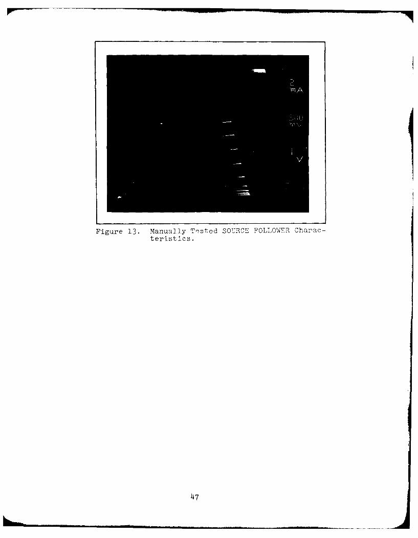
Figure 13. Manually Tested SOURCE- FOLLOWER Charac-teristics.
47

-14-.0- ----- V_ G- - __ _---
4n CALCULATED
oMEASURED 0.0
120 __0__
-1.0
8-- .-0---3 0 -
-4. -- --
-6.0
T IS -7.0
5.00
-- ~ ~ - - vs(V)-
Figure 111. Derived I-V Characterist4ics Using, thb ?'nccMESFFT DC Model.
~48

CD C
I I
49 I *

PJiuation: (21) Ia a u.1ct ,, of and a, arIvI I: a u, : :<L
obtained :'o" 1)\.:. .~, w~t V,, ,. ' : s a p :::':;.eto,: c~:nas, theC) ~ ~ ~ I a. 1 0 T'1c L.
pa::oK.:::::::: trsf:"::. Fqj:] I.:,' J : a. , 1 l~ed to (21.) aro al so sasun:J:
in Figur- !I . . ..I.., i a, ... in af tvle curves (at a g civ n ,,U.)
is doterminuzi '
R = AV, /A ] (22)o DS D)
It can be seen in Figures 1 4 and 5 that the cal Clted
mode dat a in co :aarisot to the masur'ed data di f'e, by ::
much as 0. 1 tA in the saturatetd current .....
observation of the figures as .ell as referce table
Appendix K, indiclte an approxin:iat< correl.atien o " . ' c):' mo e..
to the actual measurel eha-rctonis tics of 'i .
Dual Gate Charcteristics
By referring - to Figure 2(a), it can be seen that the "7? ,D
NOR circuit under study includes both singleo and dual gate
Nh§TiETs. The dual gate MESIqgT is identical to the single
gate MESi2 ETf except that it has two sate electrodes between
the source and drain contacts with both gates modulating
the drain current. The dual ga<te is capable of tchin
15-25% less current at V = O.Ov than the single gat I whenG S
the gate potentials are maint.aino,, at leels typical for logic
circuit oper-tion (Ref 4 :6). The cdvlanta, cs of the dual gate.
over the single gate MEMFET are (1) increased functional
capability due to the presence of two independent control
gates, such as ,nin control and sig-,nal mixing, and (2)
50

reduced feedback resulting in an improvement in power gain
and stability (Ref' 20:580).
The Dual Gate Model. The dual gate device can be visualized
as two separate single gate MEcFETs connected in cascade as
shown in Figure 16 (Ref 8:462). The output current of MESFETi,
flows directly into the channel of MESFET If the potential
between the two gates, V DS is greater than the threshold
voltage for current saturation, VDS then MESFET1 acts
as an ideal current source. The gate bias, V GS2 applied
at the second gate, controls the drain voltage VDS of the1
first transistor. To allow MESFET 2 to carry the DC current
from MESFET1 , VDS adjusts to establish the proper gate-to-
source bias V S2-V D No DC current flows into the second
gate as long as VGS 2 (positive) remains about 0.5v below
the drain voltage and the first gate bias is less than or
equal to zero (V < 0).GS 1-
In a paper by Furutsuka (Ref 20:580), the operation and
characteristics of the dual gate MESFET were treated by
combining the analyzed characteristics of two single gate
MESFETs operated under the same drain current. His study
also included high-frequency noise behavior analyzed on the
basis of Statz's model (Ref 29:559). Statz's model is an
equivalent circuit model for the MESFET and includes the noisy
parasitic elements inherent in the MESFET. Statz's model is
basically similar to Liechti's (Ref 6:289) except with the
addition of noise generators. Using Statz's model, Furutsuka
51

MESFET I ID MESFET 2 1 D
SOURCE
Figure 16. Dual-Gate MESFET Modeled as Two Single-Gate MESFET's Connected inCascade (Ref 8:461).
GRd1R 02gm GSG
0R
522

calculated the drain current ID and the channel lengths of the
carrier velocity unsaturated and saturated regions of both
MESFETs of the dual gate as a function of the gate tbus
VGS and VGS 2 . They were also calculated as a functionGSS .GS.. . ... ..1 2
of the gate bias V and V , and VDS These cliaa, c .te-- "t-i '
were obtained by adjusting ID to be the same tr'ou;.. ..
and MESFET2 with the voltage drops across the .
the source and drain resistances su.SLOCd to eau 1 V
An equivalent circuit of the dual gate
by Furutsuka (Ref 20:581), is a combination ot'
MESFET models developed by Statz (Ref 29:559) ci
parasitic elements and noise generators. Since tle
parameters of the dual gate MESFET are cf primary imr rn.
in this study, the parasitic elements and noise generatorc.
Since the DC parameters of the dual gate MESFET are of primary
importance in this study, the parasitic elements and noise
generators are shown removed, for the parasitic elements of
the single gate MESFET, in Figure 17.
Summary
In this chapter, single and dual gate models were proposed
and studied. A search of the available literature was
conducted to study the single and dual gate models. The
single gate model was correlated with actual measured char-
acteristics. Procedures developed to test the deviates of Figure
l(a) will be presented in Chapter IV.
53

IV. AUTOMATED DC PARAMETER TEST ING PROCEDURE DEVET OP !." !
In the automated testing of the devices in Figures 1 and
2, several fundamental considerations had to be established before
developing the automated test program. Additionally, it was
necessai'y to understand the test language and how it could be
used to test devices that had never before been tested on this
system. It was also required that an ability to validate the
test results be available.
The purpose of this chapter is to present the conditions
and requirements established prior to testing and the approach
and techniques (basic testing and programming) used in the
attempt to validate results obtained through automated testing.
Experimental results will be presented and compared to actual
results in an attempt to validate the developed programs.
Problems experienced in the testing will be presented as well
as the attempted approach to resolving them.
Test Considerations
Before attempting to automatically test the circuit in
Figure 1, facility with the Singer tester's Elucidate software
was required. A 4-bit accumulator fabricated at AFWAL/AADE
was tested on the Singer as an exercise in obtaining an overall
understanding of the Elucidate software as well as the system's
hardware. Conclusions drawn from this exercise are prcented
in Appendix J. The conclusions obtained from this testing
effort were used to determine the capabilities and limitations
of the system. In addition, an understanding of the methods
used to test the devices in Figures 1 and 2 manually was
54
L O M - i il . . .. . . ., i, - , l i . . . it iil II - - ir..

required before any automated testing was conducted. This is
documented in Appendix A. Conclusions drawn from this section
were used to develop programs to automate the manual process.
In order to automatically test devices at the wafer level,
it was necessary to develop a means to interface the Singer
with the devices on the wafer. A special probe card was
developed to provide the necessary interface capability.
Further discussion on the probe card is found in Appendix G.
Test and Programming Techniques
The DC parameters for the various devices within the GaAs
gate circuit which required testing are shown in Tables III
and IV. These basic parameters are characteristic of
any equivalent FET, diode or resistor in discrete form.
An organizational flowchart of the proposed program to
test the devices is shown in Figure 18. A top-down approach
was stressed in order to reduce overall complexity and redundancy.
The design of the overall program was to emphasize a well
organized approach to test the devices. Accordingly, the
program was organized in device by device sections. The DC
parameters of each of the devices on a chip were to be tested
separately before the next chip was placed under the probe
card for continued automated testing. The details of the
Singer system which influence the execution of this scheme
are discussed in Appendix B. In addition, further details
and procedures to automate the chip by chip testing of the
NAND/NOR circuit are included in Appendix H.
55

C/)
a) rC) H- 0
1~ 00
E-4HI 0 Ebo U). 4: CO
-H V) F-.-H U)
U) Uo
UE-1 co W
C/) E-AC/)0
cd E W C'-
H 0 -) D > 4-)H- fr (D H 4-:
Uf) 0 U
4-3 U)
E-f ;-4' H ~H U0 E-4
0 co 0 4-3 04:3 0 U)
Q) U.C#vi* - H U
-- U)4
)0 ) 0 0)
0~ - r 4-) -H 4-)
Y) 00 -4 >>
0 4:~-') 4' 00 U)0 a4 0 :5:)
00C) 0')H)U <~ E- W m-
0 E-4 /2C U) 0- C-7 r0
V) w))--1o U0~~~ 0I E)OH a0 )U)> u -a> 0 U) U
U)A C) z0m D E- HC3 > 0~~ P- n:2 E U)
HOO 0c " C F
4-) QZH' 1u c C
56

BEGIN
MESFET
PROGRAM
INITIALIZE I SPECIFY CHIPA DIMENSIONS
TACP# ROWS,PROB # COLUMNS
YES AL
TETEST
SOURCE FOLLOWER PINCH-OFF TEST
DC (VOLTAGE (VP) DC
PARAMETER SUBROUTINE MEASUREMENT
MEASUREMENT
CURRENT SOURCE TRANSCONDUCTANCE PROBE
DC (GM) RESISTOR DC
PARAMETER SUBROUTINE MEASUREMENT
ACTIVE LOAD BREAKDOWN INDEX TAC
DC VOLTAGE (DV) PROBEPARAMETER SUBROUTINE TO
MEASUREMENT NEXT CHIP
SINGLE GATERO AND RS xND DUAL GATE DC
SUBROUTINE PARAMETERSUBROUINE IMEASUREMENT
LIMITS DIODEDC
PARAMETERSUBROUTINE MEASUREMENT
END
MESFET
PROGRAM
Figure 18. MESFET Program Organizational Flowchart.
57

Computational and comparison subroutincs, RO, TS, LIMITS,
VP, GM, and 1V were included as such since they are comsaori to
all of the devices to be tested. Routines IDSS and VDS
(not shown in Figures 18) were includ]ed in each device ;ection.
They require simple measurements and do not require as many
lines of code as did the other DC parameters. To avoid confusion,
physical parameters will henceforth be referred to by their
variable names in the test software, e.g., IDSS instead ef I DS
System Preraration
Prior to implementing the DC parameter measurement pro.ram,
MESFET, matrix pin numbers and power supplies had to be
determined. A map of the pin numbers for each devi,.e in
Figures I and 2 was determined during construction of the
probe card. The probe card was used to interface the matrix
system of the Singer tester with the devices at the wafer
level. The pin assignments for each device are shown in
Table XII, Appendix 0, with Figure I drawn again with
pin number assignments in Figure 19. The available power
supplies to choose from are described in Appendix B. VSI,
V.2, and VS5 were chosen du- to their characteristics and
availability. The VSI and VS2 power supplies were chosrn to
apply VGS voltages. VS5 was chosen for its capability to
measure currents after it was connected to a devic,. VS' was.'7
set to a particular VDS and was then capable of measum.-
currents when the READ VS5 command was executr.d. A fulither
discussion of the Elucidate software is found in Ap cldix C.
58

V DO
47ACTIVE 33LOAD
46 SOURCE-FOLLOWER34
B 4
A C Al
SINGLE .36 DUAL GATEGATE 38 48
PROBE TEST B SCHOTTKYRESISTOR RESISTOR DIODES
C
43
2
41
CURRENTSOURCE
42
Vss
Figure 19. NAND./NOR Circuit Schematic with Matrix Pin Assignments.
59

MESFET Program Layout
In the following sections, the device sections and sub-
routines are explained in the following sequence:
1. Parameters to be tested.
2. Calculations and comparisons involved (subroutines only).
3. Algorithm CDevice and VP only).
4. Flowchart.
The order of presentation will be similar to the order in the
organizational flowchart, Figure 18.
Source Follower (SF) DC Parameter Measurement. According
to Table III, the DC parameters to be tested for the Source
Follower (SF1 were VDS, IDSS, RO, RS, VP, GM, and BV. In
order to measure IDSS, VP, and BV, it was necessary to
initialize VDS so that the device was operating in the saturation
region. From observation of the SF I-V curves in Figure 51,
Appendix A, obtained through manual testing, VDS was set
at 5.QV. This initial voltage setting was used throughout
the automated testing program for measuring IDSS, and later VP.
An algorithm used to describe the testing of SF will now
be described:
1. Condition Singer test system CSee Appendix B) for
testing using VS5=VDS, VGS=O, and the following pi- c ections.
PIN 47 = DRAIN
PIN 4_ = GATE
PIN 45 = SOURCE
At VGS = 0, the gate is shorted to GND.
2. CONNECT the voltmeter between drain and source.
60

BEGINSOURCE-FOLLOWER
DC PARAMETERMEASUREM~ENT
PIN 47 = DRAIN CALL RESETENABLE VS1; VS5
PIN 46 = GATE RO AND RS CLOSE GND;VSI;VSSPIN 45 = SOURCE SUBROUTINE CON GND 45, 46
- VS5 47
RESET
ENABLE VSI;VS5 CALL CALL
CLOSE GND;VSI;VS5 LIMITS TRANSCONDUCTANCECON GND 45;46 SUBROUTINE (GM) SUBROUTINE
CONNECT REMOVE REMOVEVMH 47 VS1 AND VOLT-AND GND FROM METER FROM
VML 45 GATE GATE
SET REMOVE GND GATE
VS5 = 5.OV VOLTMETER FROM CONNECT VOLT-
20.OMA DRAIN METER AT] DRAIN
MEASURE VDS CONNECT CALL(READ VMH 4) VS5 AND
VOLTMETER TO BVGATE SUBROUTINE
MEASURE IDSS CALL ENDSOURCE-FOLLOWER
(READ VS5 4) VP DC PARAMETERSUBROUTINE MEASUREMENT
Figure 20. SOURCE FOLLOWER (SF) DC Parameter Measurement Flowchart.
61

3. SET VS5 at 5.OV at a clamp of 20.0mA.
4. READ the voltmeter and RPINT reading: VDS at 5.0V.
5. READ VS5: IDSS at VDS = 5.OV.
6. Equate IDSS to variables for use later in the LIMITS
subroutine.
7. PRINT IDSS.
8. Call RO and RS subroutine.
9. Call LIMITS subroutine.
10. Remove GND from gate (Pin 46) and the voltmeter from
the drain (Pin 47).
11. CONNECT VSl and the voltmeter to the gate.
12. Call PINCH-OFF VOLTAGE (VP) subroutine.
13. RESET and condition system.
14. Call TRANSCONDUCTANCE (GM) Subroutine.
15. Remove VSl and voltmeter from gate.
16. GND gate and CONNECT voltemter at drain to measure
BREAKDOWN VOLTAGE (BV) subroutine.
17. Call BV subroutine.
18. End SF DC parameter measurement.
A flowchart for the Source Follower DC parameter measurement
is shown in Figure 20.
CURRENT SOURCE (CS) DC Parameter Measurements. The DC
parameters, algorithm and flowchart (Figure 21) for the Current
Source DC parameter measurement are the same as for the
Source Follower except for the different pin connections.
62
L. .. . . ..-

BEGINCURRENT SOURCEDC PARAMETERMEASUREMENT
PIN 43 = DRAIN ICONNECTPIN43 DR I MEASUREMENT IOSSPIN 41 = GATE VOLTMETER TO
PIN 42 = (READ VS5 VS4AN_I_42= GATE
CONDITION CALL CALL
TEST RO AND RS VPSYSTEM SUBROUTINE ..SfRLLoLU..E
CONNECT CALL CONDITION GND GATEVMH 43 I T CONNECTAND LIMITS TEST VOLTMETER
VML 42 SUBROUTINE SYSTEM TO
i _T__DRAIN
( SET REMOVE CALL=RANSCONDUCTANCE CALL
VS5 : 5.0V, GND FROM (GM) BV
20.0 MA GATE SUBROUTINEJ SBOTN
IMEASURE VOS REOEREMOVE ENDVSl AND VOLT-CURN
(READ VMH 4) VOLTMETER FROM1 METER FROM SURCENGATE MEASUREMENT
Figure 21. CURRENT SOURCE (CS) DC Parameter Measurement Flowchart.
63

The pin connections for the current source are the followinr:
PIN 43 = DRAIN
PIN ll = GATE
PIN 142 = SOURCE
To condition the test system for testing the CUERET SOURCE,
the following commands must be used:
RESET
ENABLE VSl;VS5
CLOSE GND; VSl;VS5
CON GND 42;4I;vs5 43
ACTIVE LOAD (AL)
DC Parameter easurement. As shown in Table III, the
DC parameters to be tested for the ACTIVE LOAD were VDS, !DSS,
RO,RS, and BV. VDS was initialied at '.0V so that the device
was operating in the saturation regicn in order to measure
IDSS. The gate and source of the Active Load are physically
connected within the circuit.
An algorithm used to describe the testing of the ACTIVE
LOAD will now be described.
1. Condition Singer system for testing using the
following pin connections:
PIN 33 = DRA!I
PIN 44 = SOURCE
RESET
ENABLE VS5
CLOSE GND; VS5
CON GND 44; VS5 33
64

BEG I NACTIVE LOAD (AL)DC PARAMETER
MEASUREMENT
PIN 33 = DRAIN READ VMH
PIN 44 = SOURCE (VDS)
CONDITION READ VS5
TEST
SYSTEM IDSSEND
ACTIVI LOADDC PAPAIfTER
ME AS URE' Ei
CONNECT CALL
VMH 33; VML 44 RO AND RS
SUBROUTINE
SET CALL
VS5 = 5.OV, BV
20.0 MA SUBROUTINEL
Figure 22. ACTIVE LOAD (AL) DC Pararieer Measurement Flowchart.
65

2. CONNECT the voltmeter between drain and source.
3. SET VS5 at 5.OV at a clamp of 20.0MA.
4. READ the voltmeter and print reading: VDS at 5.0V
5. READ VS5 and print reading: IDSS
6. Call RO and RS subroutine
7. Call BV subroutine
8. End Active Load DC parameter measurement
The flowchart for the Active Load DC parameter measurement
is shown in Figure 22.
LINEAR O!T-RESISTANCE (RO) and SATURATIO 1 (RS)
Measurement Subroutine. The parameter to be tested in this
subroutine are the linear on-resistance (ReO) and the saturation
resistance (RS) of the MESFET channel at VCS = 0. The calculation
involved in the subroutine are:
Re O VDS2-VDSII_ l , VDS2=2.OV,VDSl = 1.OV (23)
ES D2-DIl
RS VDS2-VIDl . VDS2=7.OV, VDSI=4.oV (24)
where IDl, 2 are drain currents measured at VDS1,2.
The voltage settings used in measuring RC place the
MESFET in the linear region of the I-V curve, whereas the
settings used in measuring RS place the MESFET in the saturation
region. Figure 23 graphically depicts the points to be measured.
No comparisons are made in this subroutine-only strai7-tforward
calculations are involved. The flowchart for the RO and RS
abroutine is shown in Figure 24. Prior to entering the
subroutine, the gate must be shorted to the source, VS5
connected to the drain, and the source grounded.
66

8 4VGS(V)
B 0.0
6.
5 A -0.5
2-1 .0
3
3 -1 .5
2
E -2.0
G -2.50
1 2 3 4 5 6 7 l910 1
'isD(v)A=(VSD1 (RO)=1 .OV,ID1 (RO)) E ID=1 .5% of IDSS8=(VDS2(RO)=2.OV,1D2(RO)) FzID=1.0% of IDSSC=(VDSI(RS)=4.0V,ID1(RS)) GzID=O.5%11 of IDSSD= (VDS2 (RS )=7 .OV, 102 (RS) )
Figure 23. Graphical Method Implemented on the Singer to Determine RO,RS, and VP.
67

BEGINRO AND RSSUBROUTINE(VGS=O)
DETERMNE A=SET
TANC (R) VS2-D~lVS5=VDS1 =4. OV,
20.0 MA
RREAD VMH
READ VS5
(VDS) RO A/B(IDi )
(D)SATURATION VDS2- VDSI
SET SET D=
VS5=VDS1=1 .OV, VS5=VDS2=7.OV,
20.0 MA 20.0 MA ID2 - 10
READ VMH READ VMH
(VDSl) (VDS2) RS =C/D
READ VS5RRETURN
Figure 24. LINEAR ON-RESISTANCE (RO) and SATURATION RESISTANCE (RS) Measurement Sub-routine Flowchart.
68

LIMITS Subroutine. The LIMITS subroutine was necessary
in order to provide a current limit for the VP subroutine to
use as a method to determine whether VP could be reached or
not. In order to discuss the LIMITS subroutine, it is necessary
to present the underlying rationale for its need. In the FET
theory presented in Chapter II, it was pointed out that an
accepted method to determine VP is to obtain ID = 1% of IDSS.
The VGS voltage obtained at this ID is considered to be the
pinch-off voltage, VP. In conceptualizing the method to
obtain VP using the Singer tester, it was assumed that the
possibility exists that a value of VP may never be reached
which yields ID = 1% of IDSS, i.e., the channel may fail to
pinch off due to shunt leakage or other effects. Using the
1% of IDSS method is a simple way to determine VP using a curve
tracer photographs. However,the method is not a very practical
one to determine VP when that value may be unknown when testing
a quantity of MESFETs with no curve tracer photograph available
to observe each time a test is made. Using a curve tracer
each time a test was made would defeat the purpose of automated
testing. Additionally, a curve tracer and the Singer tester
could not be connected at the same time. Therefore, another
method was considered (and eventually implemented) to Ietermine
VP.
69

The method used to determine VP was to expand the 1% of
IDSS method to a limit. If VGS was stepped from O.OV onward
with ID measured at each step of VGS, and if ID feil within
the prescribed limit, VP would have been reached. An original
limit of C0.50% of IDSS) < ID < (1.5% of IDSS) was used,
however, this was later expanded due to the decreased accuracy
of the Singer caused by a problem with the current measuring
equipment. This problem and a simple approach to resolve it
will be presented in the results section of this chapter.
The limit technique and results will also be presented then.
Another limit used to determine whether VP could be reached
or not was that of a maximum allowable VGS. This value of
VGS would be determined by obtaining values of VP from testing
several MESFETs. A typical value of VP obtained through
manually testing MESFET devices was -10.OV. This value is
obviously higher than the typical -2.5V for VP obtained in
Leichti's work (Ref 4:4). The VGS limit, however, can be
easily changed in the MESFET program to accomodate any limit.
The approach taken in developing the very simple LIMITS
subroutine was to obtain the value of IDSS measured in each
device section, multiply IDSS by lower and upper limit percentages
and print the limits. In addition, the voltage limits were set
up as comments only and used in the VP subroutine to be discussed
later. The LIMITS flowchart is shown in Figure 25. The
variables ZQ (upper limit), and ZR (lower limit), were set
equal to IDSS in the device section before the LIMITS subroutine
was entered.
70

BEGIN
LI M ITS
SUBROUTINE
MULTIPLYIDSS
BY UPPER LIMITFACTOR
MULTIPLYIDSS
BY LOWER LIMITFACTOR
INDICATE
VOLTAGE (VGS)
LIMITS
END
LIMITS
SUBROUTINE
Figure 25. LIMITS Subroutine Flowchart.
71

Pinch-Off Voltage (VP) Subroutine. The pinch-off voltage
(VP) subroutine was the most difficult to develop. Whereas
the RO, RS, LIMITS, and GM subroutines involved calculations,
VP involved a series of comparisons to reach a value of
pinch-off. The VP subroutine can be found in Figure 26.
The objective of the VP subroutine was to determine the
pinch-off voltage of the MESFET using the current limit set
up in the LIMITS subroutine. The discussion of the LIMITS
subroutine pointed out that the ID=I% of IDSS rule for VP
may not work since the Singer may not measunID accurately at
that value. VGS would then continue stepping beyond that value
of ID. Therefore, it became necessary to set up a limit.
Referring to Figure 23, it can be seen that limits of
0.5% and 1.5% of IDSS may be an approach to set up the required
limit. With VGS stepped negatively and ID measured each time,
ID may eventually reach a value within the required limit if
the MESFET ever reaches pinch-off at all. (Obtaining currents
at these low values required the high accuracy of the measuring
system of the Singer tester). If the MESFET does not plnch-off,
a method is required within the VP subroutine to limit the VG-
voltage. This limit can be determined by obtaining maximum
values of VGS for several devices. The basic idea is to detnrmlne
if VGS falls within the prescribed VGS limit. If it does,
ID at that value of VGS would then be subjected to the current
limit. If ID falls within the limit, VP is taken at the
appropriate value of VGS. If ID does not fall within the prescribed
limit, VGS is then incremented by some small volta 'c only if
VGS falls within the VGS limit. A VGS outside thi; limit
72

BEG INPINCH-OFF
VOLTAGE (VP)SUBROUT INE
INITIALIZE
VS1 VGS
READ VP
VS5 =ID NOT FU14D
READ PRINT
VMH =VGS 'VGS
-5NO PRINT
0.0 'ID='
REUR
YYES
Figure 26. PINCH-OFF VOLTAGE (VP) Measurement Subroutine Flowchart.
73

would simply indicate that the device would never pinch-off
and the subroutine would return to the main program.
Before entering the VP subroutine, items listed below
must be accomplished:
1. Determine IDSS.
2. Determine limits in LIMITS subroutine.
3. Connect VS5 to drain of MESFET.
4. Connect VS1 between gate and source of MESFET.
5. Determine initial VGS and incremental or step value
of VGS.
An algorithm and flowchart (important information only)
for the VP subroutine follow:
1. Initialize VSl to an initial value of VGS.
2. Measure ID.
3. Measure VGS.
4. Does VGS fall within a limit of, say, 0.0 and 5.0 volts?
5. If so, VP may not have been reached yet-therefore
go to 19. If not, VGS exceeds the limit and VP cannot
be reached-therefore go to 11.
6. Does the measured ID meet the conditions as specified
in the LIMITS subroutine?
7. If so, VP has been reached-therefore go to 15.
If not, VP has not been reached yet-therefore continue.
8. Print 'VGS=l.
9. Print 'LOWER LIMIT < MEASURED ID < UPPER LlMIT?
10. Go to 19: Continue incrementing VGS.
11. Print 'VP CANNOT BE REACHED'.
74

12. Print 'VGS='.
13. Print 'ID='.
14. Go to 18: Return to main program.
15. Print 'PINCH-OFF VOLTAGE (_VP) =
16. Print 'PINCH-OFF VOLTAGE (VP) =
17. Print 'ID = '.
18. Return to main program.
19. Increment VGS by a small voltage.
20. Go to 2 and repeat process until VP can or cannot
be determined.
Transconductance (GM) Subroutine
The TRANSCONDUCTANCE (GM) subroutine determines the basic
gain conductance or GM of the MESFET. VDS = 5.0V will place
the MESFET in the saturation region with VSI initially set
to O.OV. Prior to entering the subroutine, the system is reset
and then further conditioned in each device section. A
discussion of the subroutine can be described in the
TRANSCONDUCTANCE (GM) flowchart in Figure 28. GM results
are found in the results section of this chapter.
The TRANSCONDUCTANCE (_GM) will determine CM on the Singer
performing the following calculations using Figure 27 as a
reference:
GMI = (ID4-ID3)/(VGSII-VGS3) (25)
GM2 = (ID3-ID2)/(VGS3-VGS2) (26)
GM3 = (ID2-IDI)/(VGS2-VGSl) (27)
GM = (GMl+GM2+GM 3)/3.0 (28)
75

8
7 A VGS(V)0.0
6
5 -0.25
-0.5
32 -0.75
2-
-1 .0
D ~-1 .25
1 2 3 4 5 6 7 8 9 I0 11
A=(VGS4=0.OV,104) C=(VGS2=-1 .OV,ID2)
B=(VGS3=-0.5V,ID3) D=(VGS1=-1.5V,ID1)
Figure 27. Illustration of Points to be used to Determine TRANSCONDUCTANCE(GM) Using the Singer Tester.
76

BEGIN
GM
SUjQTI r[
SET READ READ READ
VS5 5.DV, VMH VMH VMH
20.0 MA (VG53) (VG52) (VGSI)
SET
VS1 VGS4, 104-ID3 103-102 102-101
D.OV, 20.OMA
READ
VS5 VGS4-VGS3 VGS3-VGS2 VGS2-V]S1
(1D4)
READ CALCULATE CALCULATE CALCULATE
VMH
(VGS4) GM1 Gm? GM3
SET SET SET
VS1 =VGS3 VSl VGS2= VS5 VGSIr= GMI GM2 +
-0.5V -1.OV,20.OM -1LSV,20.01AGM
READ READ READ AVERAGEVS5 V5 VS5ANDVS5 V5 VS5PRINT GM
(ID3) (102) (101) (MILLIflHOS)
CRET=URN
Figure 28. TRANSCONDUCTANCE (GM) Measurement Subroutine Flowchart.
77

BRFAKDOWN VOLTAGE ( ,V) Subroutine. The BRIEKDOWN VOLTAGE (-V)
subroutine was developed to determine the break jown voltage
(BV) of a MESFET at VGS=0.0V. A practical approach (which
is highly dependent on the current measuring accuracy of the
Singer) is to determine BV based on a major change in the slope
in the saturation region. A visual description as shown in
Figure 29 will aid in the discussion of the BV subroutine
flowchart, as well as an algorithm as shown below.
a. Connect VS5 and voltmeter across drain and source of
MESFET.
b. Ground gate unless MESFET is the ACTIVE LOAD. BREA3K-
DOWN VOLTAGE (BV) Algorithm:
1. Initialize VS5 = VDSI at 5.OV; ZV = 0.5; ZF = 2.0
2. Measure IDl (n=l).
3. Measure VDS1 = 5.OV.
4. Increment VS5 by 1.OV (VS5 = VDS2 = 6.OV)
5. Measure ID2 (n= 2 ).
6. Measure VDS2.
7. Slope(l)=(VDS2-VDSI)/(ID2-IDI)=:Store Slope(l) at n=2.
8. Increment VS5 by 1.OV (VS5 = VDS3. = 7.OV)
9. Measure ID3 (n=3) •
10. Measure VDS3 = 7.OV
11. Slope (2) = (VDS3-VDS2)/(ID2-IDl) : Store Slope
(2) at n= 3.
12. Is Slope (2) greater than Slope (1) by more than
1000.0? If so, BV = VDS3 = 7.OV. If not, continue
13. Increment VS5 by 1.OV. (VS5 = VDS4 = 8.OV)
78

THE AUTOMATED Dr PARAMETER TESTING OF GAAS MESFETS USING THE SI-ETCfUjSEP 80 T L HARPER
UNCLASSIFIED AFIT/EE/GE/80-7
EU~~wl WE WEHIHHEOEEEBEEEEEEEEEEEEEEEEEEEEI
EEEEEEEEEEEEEE

9.V vc:;=C'.'
- VDS
.0
1. 2! 3!c 4! 5.- - '. 1 -.
Figure 29. Illustration of Method to D-etermineBREAKDOW14 VOLTAGE (BY7.) at VGS=n0.OVon the Singer.
79

SET VS5=5.OV
ZV = 0.5
ZF = 2.0
(n=l)? nnl
READ VS5:ID (1)YEREAD VMH:VDS ()
:ED 2~~~ AVDS D2 VSVS5 = VS5 + 1.OV[
(n=n+1) )
1111 111AID = ID2 I11.(n=2) Z1=ZB-Z1A=READ VMIf
ZK=READ VS5:ID(ri+])l
ZM =AVDS/AID
(n=2) AVDSZhZI=ZE
ZE=READ VMH:VDS(n+l)
ZB = ZE
ZF =0.5 AID ZJ =ZJ -ZK
3
Figure 30. Breakdown Voltage (BV) Measurement Subroutine.
80

1 3
AVDS =ZA =ZA - ZE ZI =AVDS/LID
AID =ZJ ZJ -ZKj ZI =ZI - ZM
"'IIZA =AVDS/AID .< -100
2 O.O<ZA<1000.OO
YES
NO
PRINT BV
RETURN
Figure 30. Continued.
81

14. Measure ID4 (n=4).
15. Measure VDS4 = 8.OV.
16. Slope (3) = (VDS4-VDS3)/(ID4-ID3): Store Slope (3)
at n=4.
17. Is slope (3) greater than slope (2) by more than
1000.0? If so, BV=VDS4 = 8.0V. If not, continue.
18. Increment VS5 by l.OV (VS5 = VDS5 = 9.OV).
19. Measure ID5 (n=5).
20. Measure VDS5.= 9.0V).
21. Slope (4) = (VDS5-VDS4)/(ID5-ID4): Store Slope (4)
at n=5.
22. Is Slope (4) greater than Slope (3) by more than
1000.0? If so, BV = VDS5 = 9.OV. If not, continue.
23. Increment VS5 by l.OV (VS5 = VDS6 = 10.OV).
24. Measure ID6 (n=6).
25. Measure VDS6 = l0.OV.
26. Slope (5) = (VDS6-VDS5)/(ID6-ID5): store Slope (6)
at n=4.
27. Is Slope (5) greater than slope (14) by 1000.0?
If so, BV = VDS6 = 10.OV. If not, continue.
It seems, a priori, that the BV subroutine in theory is a
valid approach to determine the breakdown voltage of a MESFET
on the Singer.
82

SINGLE GATE and DUAL GATE DC Parameter Measurement. The DC
parameters to be tested in the SINGLE GATE and DUAL GATE
(Figure 1) device sections are VDS, IDSS, RO, RS, VP, GM, and
BV. In order to test the devices separately, one of them
must be pinched-off before the other can be tested. At pinch-
off device ideally represents an open circuit. Therefore, a
VP must be assumed for one of the devices. A simplified
algorithm is shown below:
1. Assume VP = -3.OV for DUAL GATE.
2. Pinch-off SINGLE GATE using VP program.
3. Remove -3.OV from DUAL GATE.
4. Test DUAL GATE DC parameters.
5. Keep DUAL GATE at VP and remove VP from SINGLE GATE.
6. Test SINGLE GATE DC Parameters.
In the above algorithm, the DUAL GATE is set at an assumed VP
of -3.OV and is considered to be an open circuit as indicated
above. VP for the SINGLE GATE is then determined. Pinch-off
at an assumed -3.OV is then removed from the DUAL GATE. The
DC parameters for the DUAL GATE are then tested. Afterward,
the DUAL GATE is kept at VP and then VP is removed from the
SINGLE GATE. The SINGLE GATE's DC parameters are then tested
(except VP). Figure 31 is the flowchart for the SINGLE GATE
and DUAL GATE DC Parameter measurement and is self-explanatory.
The main problem that may be encountered in testing the two
gates is that the assumed VP for the DUAL GATE may not be
correct. VP may actually be higher or lower than -3.OV. No
special provision has been developed to reset VP if a higher
value turns out to be needed. It may be necessary to study
83

BEGINSINGLE GATE (A)
DUAL GATE (B AND C)DC PARAMETERMEASUREMENT
PIN 34 = INPUT B(DGB) CALL CONNECTPIN 35 = INPUT C(DGC) VS2 TO SGAPIN 36 = GND (SOURCE) LIMITS ANDPIN 37 = !TNPUT A(SGA) SET VS2=VP, 20.0 MAPIN 44 = DRAIN SUBROUTINE (OBTAINED FROM VP SUB.)
RESET DIS GND FROM GAIE CONNECTENA VSI ;VS2;VS5 OF SGA; GND AT DGB
CLOSE GND;VSI;VS2;VS5 DIS VHH FROM DRAIN DISCONNECTCON GND 36; 37;VS2 34; CON VMH TO GATE OF SGA |VMH FROM SGA
35; VS5 44 ANDCON VMH 44; VML 3C CONNECT TO DRAIN
APPLY 5.OV to DRAIN: CONNECTSET VS5:5.OV,20.OMA VSI TO GATE READ VS5 (IDSS)
ASSUME VP=-3.OV for DGB OFand DGC: SGA (DUAL GATE B)
SET VS2=-3.OV,20.OMA
READ VH (VDS) CALL IDSS=IDSS * 1000.0 (MA)
READ VS5 (IDSS) PINCH-OFF VOLTAGE (VP)SUBROUTINE ZQ = IDSS
(SINGLE GATE) (PINCH-OFF SGA) ZR = IDSS
IDSS=IDSS*1000.0(tIA) DISCONNECT CALL
ZQ = IDSS VS2 FROM DGB AND RO AND RS
ZR = IDSS DGC;VS1 FROM SUBROUTINE
DGA (VGS=O)
Figure 31. SINGLE GATE (A) and DUAL GATE (B and C) DC Parameter Measurement Flowchart.
83

CALL
LIMITS
SUBROUTINE
DISCONNECT CONNECT CALLGND FROM DGB GND AT DGB RO AND RS
CONNECT AND SUBROUTINEVS1 TO DGB (34) VMH AT DRAIN (VGS=O)
DISCONNECT CALL CALLVMH FROM DRAIN BREAKDOWN VOLTAGE (BV) LIMITS
CONNECT SUBROUTINE (DGB) SUBROUTINEVMH TO DGB (VGS=O) (DGC)
CALL DISCONNECT DISCONNECIPINCH-OFF VOLTAGE (VP) GND FROM DGB GND FROM DGC
SUBROUTINE AND CONNECT CONNECT(DGB) GND TO DGC VSI TO DGC
CALL READ VS5 (loss) DISCONNECITRANSCOIDUCTANCE (GM) VMH FROM DRAIN
SUBROUTINE (DUAL GATE C) CONNECT(DGB) VMH TO DGC
DISCONNECT IDSS=IDSS*1OOO.O(MA) CALLVS] AND VMH PINCH-OFF VOLTAGE (VP)
FROM ZQ = IDSS SUBROUTINEDGB ZR =.IDSS (DGC)
L 2
Figure 31. Continued.
84

CALL
D TRANSCONDUCTANCE (GM)
E > SUBROUTINE
DISCONNECT SET DI SCONNECTVS1 AND VMH FROM VS2 AT VP
DGC FOR DGB; VSI FROM SGA;CONNECT GND AT DGC VS3 AT VP VHFO G
ANDVMH FROM SGAVMH.AT DRAINI
CALL CALL CONNECTBY RO AND RS
SUBROUTINE SUBROUTINE GND AT SGA
RESETENA VSI;VS2;VS3;VS5 DISCONNECT CONNECT
CONNECT GND FROM SGA;GND AT SOURCE AND CONNECT VMH AT DRAIN
DGA VSI AT SGA
CONNECTVS2 AT DGB DISCONNECT CALL
VMH FROM DRAIN:
VS5 AT DRAIN CONNECTVMH AT SGA SUBROUTINE
CONNECT CALL END
VMH AT DRAIN GM SINGLE GATE AND
AND SUBROUTINE DUAL GATE DC
SOURCE PARA>.W[TER MEASUREMENT
Figure 31. Continued.
85

several dual gate devices using the curve tracer to obtain
an idea of what value of VP is needed.
DIODE DC Parameter Measurement. The DIODE device section
was written to measure the forward threshold voltage (VI') and
reverse threshold voltage (VR) of the three series Schottky
diodes in Figure 19. An understanding of D3ODE can 1L obtained
from Figure 32 which illustrates the basic scheme used to
de-ermine V., and VR usingz the Singer. A flowchart for DIODE
and the system connections for determining VF and VH are shcw;n
in Figure 33. Since DI0DE was- not, actually tested, the currents
indicated in Figure 32 are subject to change after required
experimentation and analysis with the Singer and a curve tracor
are carried out. DIODE will now be explained.
According to DIODE, VF can be obtained by apply'inr V"5
and the voltmeter across the diodes as shown in Figuro 1 (a).
Using conventional diode theory, VF is determined at the point
where current I begins to flow after V Is increased to
some value. Since I and V are variable from circuit to circuit,
a method to determine VF using the Singe is necesxaty. A
limit such as 0.5 < I < 1.0 mA was chosen ( subjt, ct to cnanr T)
to determine VF. V is to be increased by soei, a:i-oirit until i
falls within the set limit. When this occurs, tKe v'i]u cr" V
is taken to be VF. The sarre method applies to VE the
current limit is -1.0 < I < 2.0 mA which is subj,,t 2 ' i'h,
after experimentation with the Singer and a curve tr'icev. ' C
curve tracer could be used as way to determine the actual
VR or VF in order to validate DIODE.
86

vcV -O!E l*2.6pi~
4'v
Figure 32. Illustrdtion of Current Limits to Determine VF and VR on theSinger.
87

DIODE
TESTVF
-R
PIN 45 ANODE (A)I 45=ANOIDf (A)
PIN 43CATHODE(C) PIN 43CATHODEC)1
RESET RESET ENABLE VS5ENABLE VS5 CLOSE GND; VS5
CLOSE GND;VS5 CON GND 45;VS4 43CON GND 43;VS5 5§ VMH 413; VNIL 45
SET SET
20.0 MA 20.0 MA
MtEASURE APPLIED MEASUR APPLIED
VOLTAGE VOLTAGE v =vp%
(READ Wifl 4) (READ VMH 4) AT I
MEASURE CURRENT MEASURE CURRENT
DRAWN BY DIODES DRAWN BY DIODESEN
RA S(READ VS5 4) DIODE TEST
0iue3. DIOID FlwA r toS TeV VF -1n0 VP on theSMAgYrS
AT8

45
A
VM B +
43(a)
45
A -
VM+B+
C
43(b)
Figure 34. Required Singer Connections to Determine VF and VR. (a)Forward Threshold Voltage Connection. (b) Reverse Thres-hold Voltage Connection.
89

BEG IN
RESISTANCE
MEASUREMENT
MEASURE MEASURE
TEST PROBE
RESISTOR RESISTOR4 1,PIN PIN
ASSIGNMENT: ASS I GNMENT:
44;48 44;38
RESET RESET
CONNECT CONNECT
RMH 44; RML 48 RMH 44; RML 38
READ READRMH 4 RMH 4PRINT PRINTREADING READING
END
RESISTANCE
MEASUREMENT
Figure 35. TEST and PROBE RESISTOR Measurement Flowchart.
90

TEST and PROBE RESISTOR Measurement. A method to test the
resistance values of the TEST and PRODE RE OSTOR is preented
in Figure 35. The Singer tester is capable of directly
measuring the resistance of discrete as well as integrated
resistors. The implemented program of the flowchart of Figure
35 is presented in the MESPET prcgram, Appendix I.
Summary
The algorithms and flowcharts presented in this chapter
were developed to automatically test the DC parameters of the
devices shown in Figure 19. The considerations made prior to
the development of the actual MESFET program (Appendix I)
were discussed as well as the test and programming techniques
used. In the next chapter, results obtained from the automated
testing of the DC parameters of Figure 19 as well as the
problems encountered will be presented.
I
91

V DC PARAMETER MEASUREMT RFL1JLT-2 AUD A ALY.L
The purpose of this chapter is to present the DC parameter
results obtained throu&h automated testing of devices of the
NAND/NOR circuit of Figure 17 using the Singer automated tester.
The results were obtained through application of the algorithms
and flowc rts presented in Chapter IV and then converted to
a coded program as shown in Appendix I.
In order to provide a means to verify the validity of the
results obtained with the Singer, a Tektronix Model 576 curve
tracer oscilloscope was used. The steps used to perform testing
are presented in Appendix H. Values of ID, obtained at VDS = 5.OV
with V as an input voltage, were extrapolated from the curveGS t
tracer photograph. These results will be presented in th~e form
of transfer characteristic curves for comparison with the
values of ID at VDS = 5.OV with VGS as an input voltage using
the Singer.
The original strategy in the developmental stage of testing
the MESFETs in the MESFET program was to test the devices
developed by AFWAL/AADE. However, since an adequate quality
of working devices was not available and since experimental
testing involved possibly destroying these expensive devices
(at the wafer level, constant probing of the devices was
necessary) a decision was made to validate the program using
another device. The device chosen was a packaged, n-channel,
commercial silicon JFET whose DC operating characteristics were
similar to those of the MESFET. This device was easier to
test (since the JFET was packaged, no probes had to be used),
and had the advantage that obtaining pinch-off was assured.
92

This strategy minimized the necessity of constantly probing
and damaging the GaAs chips and reduced the risk that tYt
probes in the probe card might be bent out of alignment
during initial program development.
After proving the validity of the MESFET prog;ram using the
JFET (results are shown in the followin,- section), tests were
then conducted using the GaAs MESFET devices at the wafer
level. The results obtained using the JFET will now be
presented.
JFET DC Parameter Measurement
The Texas instruments JFET, type 2N3819, was inoerted
directly in the performance board (Figure 57) using the sar
pins as for the SOURCE FOLLOWER. The testing was performed
without the inclusion of the ability to automatically step
across a wafer using the TAC probe. The Singer system
was prepared (Appendix H), a curve tracer photograph of the
I-V curves of the JFET obtained, and finally the SOURCE FOLLOWER
portion of the MESFET program applied to test the JFET.
The JFET exhibited excellant characteristics as shown in
the curve tracer photograph of its I-V family of curves, Figure -0.
As can be seen, the JFET exhibited excellant linearity in the
ohmic and saturation regions, including the ability to reach
pinch-off. The DC parameters of the JFET were also tested on
the Singer tester using the MESFET program. The results obtained
for both methods are shown in Table V, and Figure 37.
From Table V, it can be seen that ID measurement errors
seem to increase as VGS is increased negatively (except at
93

Figure 36. JFET I-V Characteristics
Table V. JFET DC Parameters
DEVICE: 2143819 JFET
.METHOD
DC PARAMETER CURVE TRACER SINGER %ERROR
VDS(V) 5.0 4.99 0.2IDSS(mA) 4.8 4.56 5.15RO(Ohms) 900 987 7.9RS(Ohms) 15,000 16,042 6.495)LIMITS VP@l% of IDSS 0.1%<ID<l.1%VP(V) -1.6 -1.*38 16.2ID(mA) 0.05 0.045 11.1GM 3.07 3.65 15.9VGS(V) ID(rnA) I D ( A) ' Error0.0 4.8~o -T.75.15-0.5 2.40 2.29 4.6-1.0 1.00 0.75 4c5-1.3 0.40 0.045 78H-1.5 0.20-- -- - --1.6 0.05
914

-S SINGER - -- --- - _ - 5.0 -- --
0 CURVE TRACER
-. ---- -- 2 .-
2.0
-- 2.0 -1.5 -1.0 -0.5 0.0
* * VGS(V)
Figure 37. JFET Transfer Characteristic.
95

IDSS). In addition, the VP subroutine determined VP=-l.376V at
ID=0.0 45mA. This value of ID is about 0.985 of IDSS, and is
still within the indicated limits set up in the LIMITS subroutine.
From Lhe curve tracer measurement, VP=-l.6V at ID = 0.05mA
which is 1.04% of IDSS. As can be seen, VP was reached at
a smaller VGS on the Singer than in the curve tracer data.
The VP results for the JFET, however, prove the concept that
an approximate value of VP can be obtained using the limit
method. With improved accuracy of the system, the actual and
experimental values of ID and VP (as well as 'GS), will improve
in agreement.
The linear and saturation resistances are shown in the table
with the indicated percentage error including the transconductance
CGM) of the JEET. The techniques used to obtain these parameters
were discussed in Chapters II and IV.
As pointed out above for values of ID at each VGS voltage
in Table V, ID measurement errors (actual vs. experimental
errors) increased as VGS increased negatively. This problem
become significant as the channel of the MESFET approached
pinch-off. Significant problems were later experienced with
the Singer system which deserve attention. These will be
presented in the next section and the method to resolve the
probleis will be pointed out and discussed.
Singer Tester Problems
The VP subroutine is highly dependent on the current measuring
system in the Singer. A calibration program, CALIB (see
Appendix H), is available on the Singer and yielded the following
results for a current measurement of 1.0 ampere only, using VS5:
96

Sensitivity Deviation = 0.51%
Zero Offset = 0.13%
Accuracy for this particular supply below 1.0 ampere was not
available and could be assumed to be much worse. However,
after attempting to calibrate VS4, the possible alternate supply,
it was decided not to use it due to the following characteristics
at 100mA:
Sensitivity Deviation = 100%
Zero Offset = 22.03%
Sensitivity deviation and zero offset were much much worse
at lower values of ID.
The problem in the current measuring capacity was believed
to lie in the automatic ranging amplifier within the Singer.
In the early development of the 1VSFET program, power supply
VS1 encountered problems. The current ranging circuitry
of the supply overloaded and several components were destroyed.
mle ranging amplifier obtains output from the supply and auto-
matically assures that each current and voltage reading is taken
at the highest gain setting to assure the most accurate results
(Ref 21). Following the VSl failure, it was assumed that when
a READ command was encountered, more current beyond the specified
output current was read, and this in turn reduced the capability
of the ranging amplifier to produce accurate measuc'ro:mnts. It
was felt that the problem could be cured by zhip~pin.; the amplifier
back to the manufacturer for repair, but this could liave taken
weeks. The decision was made to calibrate V5 furt..r to provide
more accuracy, but this did not seem to be sufficient. The VPI
97

rangins circuitry was repaired but the accuracy was reduced
significantly. The board was then reolaced entirely, but this
did not solve the current measuring problem.
Throughout the testing of the JFET (and later the MESFET)
an attempt was made to develop a method to resolve the accuracy
problem. The problem could not be removed immediately and given
the urg ent nced to test MESFET devices, a simple method to
introduce error factors into the program was conceived, This
method, however, turned out to be very difficult and eventually
unpredictable when more than one device was tested, The error
factors were determined by obtaining curve tracer rhotoeraphs of
a particular MESFET's I-V curves, Later, the same MESFET was
applied to the Singer tester for testing. Values of ID at a value
of VGS (in 0.1V steps) were obtained with VDS=0.5V. The same
values of VGS (at VDS = 5.OV) were observed on the photorraph
and the value of ID at that VGS was recorded. The error factor
was obtained by the following:
ERROR FACTOR = Actual ID/Exoerimental TD (29)
An example and further discussion is presented in Appendix L.
NAND/NOR Gate DC Parameter Measurement
The remainder of this chapter will be devoted to the presenta-
tion of results obtained from thae testing of the GaAs ERSFET
circuits of Figure 19. It is recognized that the data are corrupted
by the current measurement inaccuracy of the Sin,-er system. The
devices tested were the SOURCE FOLLOWER, CURRENT SOURC, and
ACTIVE LOAD. The DC parameter, BV, was not tested due to the
accuracy of the equipment. The SINGLE GATF, DUAL CATE, and
98

DIODE devices also were not tested on the SinCer due to this
problem. The TEST and PROBE Rr.I ...I....S were not tested, but
could be easily tested using the simple program presented in
Chapter IV.
An attempt will be made to demonstrate that the :E,7'ET
program is theoretically sound. This demonstration was attempted
in the JFET test, and it was hoped that, g!ven the equi ,,ment
problem, tests of the MESrET devices would also be successful,
The most important and sophisticated parameter to measure was
the pinch-off voltage of a device, An attempt was made tc reach
this point despite the current measurin- error of the f'inger.
With the equipment problem unresolved, ID measurements made at
each VGS sten must be in error and in turn VP will obviously
be in error, A statistical analysis of DC parameter data obtained
from the tests will not be presented since the validity of the
numerical results is questionable.
SOURCE FOLLOWER DC Parameter Measurements. Several SOURCE
FOLLOWERs were tested using the curve tracer prior to testing
them on the Singer. Testing the devices on the curve tracer first
provided the opportunity to determine which devices would be
favorable to test on the Singer. SOURCE FOLLOWERs that exhibited
somewhat linear characteristics in both the saturation and ohmic
regions as well as those that achieved p nch-off w.re selected
for further Singer testing. The primary objective in the MES"ET
program development was to simply obtain a device that exhibited
a favorable I-V curve and test it further on the Singer. Many
devices' I-V curves indicated that they would never reach pinch-
99

off or would reach breakdown pre.atu'ely, These devices
were not aggressively sought after since the VP was the most
important (and difficult) parameter to obtalin on the Pl ayer.
As can be seen in Table VI, VF = -3.5V at 0.11mA was
obtained using the curve tracer wlereas VP could not be
reached using the Singer. Tlhe indicated limit set to
reach the value of VP = -3.OV at ID = .i6787 mA demonstr2tes
theinaccuracy of the system. It can be seen that the ID
obtained is actually 10,93% of IDS. The proner VP would
have never been reached using the limit of 0.5,% < ID < 1.57,
It is important that the same limit to test VP for every
MESFET is used. If not, the purpose of testin many devices
automatically would be defeated since a standard limit must be
used. With the Singer's inaccuracy, it was impractical to attempt
to define standard limits to obtain VP. Limits of as much as
0.5% 1 ID e 10.0,0 were used to test the SOURCE FOLLOWERs (as
well as other MESFETs). ID reached the limit eventually, but
the wrong value of VP was obtained. A limit such as the one used
above is very inaccurate whereas a limit such as 0,5 - iD i. 1,5,
increases the accuracy of VP. An TD of 0.4mA (2.5% of IDSS) for
VP = -3.5V was obtained using the curve tracer which was 2.5"
of IDSS. It seems at this point that even if the Singer were
functioning properly, standard limits would not be practical
VP(Figure 33) was achieved using the curve tracer regardless of
the theoretical 1% of IDS rule. It also seems now that this
problem could be in the accuracy of the curve tracer or the device
itself. The problem demonstrates that a standard limit for
100

Figure 38. SOURCE FOLLOWER 'A' I-V Chaiacteristicz.
Table VI. SOURCE F01,LOWER 'A' DC PARAMEH,2
DEVICE: SOURCE FOLLOWER
METHOD
DC PARAMETER CURVE TRACER C ERROR
VDS(V) 5.0 4.99 0.2IDSS(mA) 16.0 16.18 2.098RO(Ohms) 167.0 140.0 19.28RS(Ohms) 7500.0 7375.0 1.69LIMITS VPS2.5r OF IDSS 0.5<ID<1. 5 - --
VP(V) -3.5 -3.0 16.7ID(mA) O.4 1.69 76.3GM(mill imho) 6.0 .70 5.2
0.0 16.0 16.18 1.os5-0.5 12.6 12.87 1.6-1.0 9.6 9.88 2.52-1.5 7.0 7.26 3.71-2.0 4.4 4.95 11.17-2.5 2.0 3.01 50.5-3.0 0.8 1.68 52.6-3.5 0.5 ----
101

17.0
~16.0
- oCRVE TRACER -- 14.0
13.0
12.0--
9. 10
- 3.0 ~
5.0
3.
- ~ 2.0
-3.5 -3.0 -2.5 -2.0 -1.5 -1.0 -0.5 0.0
VGS(V)
Figure 39. SOURCE FOLLOWER 'A' Transfer Characteristic.
1.02

Figure 40. SOURCE FOLLOWER 'B' I-V Characteristics.
Table VII. SOURCE FOLLOER 'B' DC PARAME'-
DEVICE: SOURCE FOLT q'
METHOD
DC PAR.ANQ:R' CURVE TRACER SINGER ERROR
VDS(V) 5.0 4.99 0.2IDSS (riA) 8.8 9.66 8.9RO(ohms) 192.3 215.8 10.98RS(ohms) 15,000 i!,000 29.CLIMITS VP@ 2.27% of iDSS 0.5 '<ID<1. ---
VP(V) -3.5ID(mA) 0.2GM(millinbios) 3 .47 2.12 11.2vGS(V) ID (mA) D Q>1> . -E0
0.0 9.0 9.66 6.i5-0.5 7.2 7.70 6.58-1.0 5.4 6.44 16.15-1.5 3.8 4.61 17.7-2.0 2.2 3.27 32.75-2.5 1.0 2.16 5 .75-3.0 0.4 1.50 73.40-3.5 0.2 1.29 8L.57
103

S SINGER 10.0
o CURVE TRACER -~- ---- 9.0
- 8.0
- - - ---- ------- -- --- 7.0 --
- - 6.0
- ---- - - 5.0 _
4.0
0 - 2.0
-3.5 -3.0 -2.5 -2.0 -1.5 -1.0 -0.5 0.0
Figure 41. SOUIRCE FOLLOUEF IT-, Tr-ns 2er ctr.i.
1014

d eti C' :I L Ii n - VP I.: 2 l U b1 J' II t-b ci. o. th a'
with accuracy in c ur t- Un,':t:,t :.d erer: : so wit:.
the accuracy.
Other t)a aeter: do:ictin[: SOURCE D F,:, XE.] 'A' c'ta
be seen in the table. FiCure 19 dLrlct VII vor, .''i .. Th Ifigure iniicat-es that the Slnrer shows sore acurac7 ii [:1'V.
currents. but is low at lo ,, cur-"n "tso.r, I.>aff * A
percentare error in the table indicates the accua tCy I'b:
ID is decreased.
SOURCE -OLLOER 'B' results are S iown in Table Vi atl"
Figures 4I0 and 41. The limit was set at 0.5C ID 1.5 for
the Singer. Id never reached within the set lirit an re:ore
VP was not obtained. The rrogram sim,ly by...a.E.. '-'w " xced
VP. The value of ID at VS = -3.5V is 1.2a6l0mA. a' i'"' of
IDSS. This indicates that the standard llmit would net arr"y
with the Singer's accuracy. Figure 41 depicts VS versus
ID with the percentage error indicated in Table VII including
other measured parameters.
CURRENT SOURCE DC Par ameter '.. easurement
A CURRENT SOURCE was tested using the Singer tester
with the results shown in Table VIII. The I-V characteristics
of the MESFET as measured on the curve tracer are shwr
in Figure 42.
As can be seen in the table, the percentare error varies
somewhat and does not show consistency as ID decreases. A
graphical representation can be seen In the transfer characteristics
of the CURRENT SOURCE as shown in Figure 4h,
105
" i n .. . .. . i . . I i a - 1 I

Figure 42. Current Source I-V Characteristics.
Table VIII. CURRENT SOURCE DC Parameters.
DEVICE: CURRENT SOURCE
METOD
DC PARAMETER CURVE TRACER SINGER
VDS(V) 5.0 4.99 0.2IDSS(mA) 11.6 14.29 18.2RO(ohms) 166 182 9.6RS(ohms) 7500 4525 39.7VP(V) 3.0ID(mA) 0.6GM(millimhos) 3.7 4.451 16.3Limits VP@ 3.9% of IDSS 0.5%<ID<1.5'
VGS(V) ID(mA) TD(mA) ERP%, R
-0.0 11.6 14.29-0.5 9.0 11.4 21.0-1.0 7.0 8.80 20.45-1.5 5.0 6.38 21.6-2.0 3.0 4.27 29.7-2.5 1.6 1.62 1.20-3.0 0.6 1.38 56.5
106

ASINGER 15.0
--13.0
- - -12.0
-------------- ----- *----~- - -. 11 .0 --
- -- ---- 10.0
8.0
-6.0
- ------- -- -- 5. 0- -- -
4.0
- - * -. -- - 2.0
-3.5 -3.0 -2.5 -2.0 -1.5 -1.0 -0.5
- -- VGS(V) -- - ---
Figure 43. CURRENT SOURCE T.ransfcor Caa~k
107
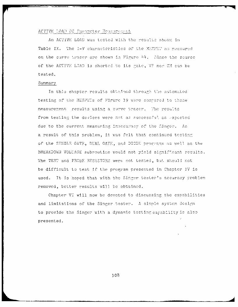
ACTIVE LOAD DC Pai , meter_::,r<,.;,r.t
An ACTIVE LOAD was tested witi the results shown in
Table IX. The I-V characteistics of' the a.;i(.E as measured
on the curve tracer are shown iu Figure 44. Gince the source
of the ACTIVE LOAD is shorted to its gate, VP nor C7 can be
tested.
Summary
In this chapter results obttined throurh the automated
testing of the MESFETs of Fifure 19 were corared to those
measurement results using a curve tracer. The results
from testin- the devices wer-e not a- successful as ,xoccted
due to the current measuring inaccuracy of the Singer. As
a result of this problem, it was felt that continued testinr
of the SINGLE GATE, DUAL GATE, and DIODE ororams as well as the
BREAKDOWN VOLTAGE subroutine would not yield signifIcant results.
The TEST and PROBE RESISTORS were not tested, but should not
be difficult to test if the program presented in Chapter IV is
used. It is hoped that with the Singer tester's accuracy problem
removed, better results will be obtained.
Chapter VI will now be devoted to discussing the capabilities
and limitations of the Singer tester. A simple system desi-n
to provide the Singer with a dynamic testing capability is also
presented.
108
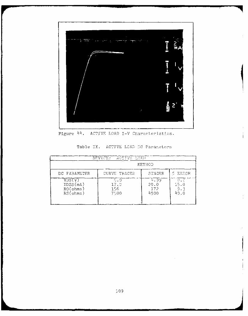
Figure 44. ACTIVE LOAD I-V Characteristics.
Table IX. ACTIVE LOAD DC Parameters
DEVICE: A CIf Iv LCAD
METHOD
DC PARAMETER CURVE TRACZDI SINCER ERDOR
VDS(V) 5.0 4.99 0. 2IDSS(mA) 17.0 20.0 15.0RO(ohms) 156 172 9.3RS(ohms) 7500 4500 40.0
109

VI. CAPAhTLI'TES A'!D IOF T!' H 2TUGZ- T :7 T'
In the previous two chapters, procedures to test the DC
parameters of an JFET and MTISFET usine the Singer tester were
developed and measurements obtained for most of these parameters.
An attempt was made to prove that the Singer was capable of
testing the static DC parameters of a JFET and MESFET. This
capability had never been proven before. The results obtained
were not spectular since the Sin cr encountered measurement
accuracy problems. With an improved measuiement accuracy,
a better idea of the Singer's canabillty in the area of JFKT/
MESFET DC parameter testin7 w!l be obtained.
The purpose of this charter is to study the capabilities
and limitations of the Singer tester. These will be determined
by information published in the Singer manual (Ref 21),
tests conducted to study the voltage output characteristics
of the Singer and the principle results of the testing, of the
MESFET (Chapter V) and the4-bit accumulator (Appendix J).
Published Snecificatlons of the Singer Tester
According to the preliminary draft written by Sin e- fcr the
tester (Ref 21), the system is capable of performint full DC
parametric testin7, data plotting, data logging, and data analysis
on semiconductor circuits (integrated and discrete) as well as
resistors (integrated and discrete). These tests ci. be performed
at the wafer level using the TAC Automatic Probe Unit (,ee3
Appendices C and G) or at the packaged circuit lew,l. PackaFed
circuits can be directly inserted in the system's ptrformance
board. Singer develoned the tester for the initial uirpose
110

of testing transistors, integrated circuits and resistors.
The Sin er tester has the capability to. perform DC measure-
ments on the devices indicated below.
Bipolar Transistors. The following DC parameters can be
measured on the Singer:A. E FE (small-signal current gain) as a function of IB
(typical I = 100A to 100mA).
B. lHFE as a function of T (typical I = 100iA to 100mA).
C. VBE as a function of IE (typical IE = 10PA to lOmA).
D. BVEBO (typical 0 to 10V, 0 to ImA, with independently
adjustable voltage and current limits).
E. BVCBO (typical 0 to 100V, 0 to lmA, with independently
adjustable voltage and current limits).
F. BVcE 0 (typical 0 to 32V, 0 to lmA, with independently!
adjustable voltage and current limits).
G. BVcE S (typical 0 to 32V, 0 to lmA, with independently
adjustable voltage and current limits).
H. BVDS (typical 0 to 100V, 0 to lmA, with independently
adjustable voltage and current limits).
I. Vcs(sat ) as a function of Ic (100PA to 100mA),
J. I CB as a function of VCB 0 (typical 10CIiA from 0 to 12V).
K. ICS as a function of VCS (Typical !00pA fron 0 to 32V).
L. I EB as a function of VEB 0 (typical 00pA frc:r 0 to 6V).
Integrated Circuits. The following DC parameters for_ medium.-
scale integrated circuius can be measured on the Sin-e0r:
A. Input leakage currents.
B. Input level voltages.
1i1

D Outntu v
E. Output fa n ,1.
F Total dcve;
Gi 1 ru1' Iy v. . ...1.,.•. II Supply t'-- "
Integrated (uncl V1)f Iet'' '-'
)'"!:. . ' i} . .. ] '' ':' q' .. 't'.t
istics can be deter ,-I -d i i t fio,'
A. Abso.ute( v nlue of' rc.- , ,..° (t',i'i- ' K o-" to S . o s)
B. Ratio between,, an, two r,-s ,
For further infoirmat ion ccn , -n n:0 - sec-icat oni aIZ
characteristics of the 7i~r<',t.,cr, ... Ar-nendix P.
S ingc-er V ol.t a 7 - Out rt h~' 1eItT C ' sKP 1o-e 17 1t r-
Capability
Tests were conducted to ethe voltage output
characteristics of the Singer tester. Of primary interest in
the study of these c .aracteist. cs is the frequency at which
the Singer power supplies can be turned on and off which
results in the formation of square waves. To form these square
waves requires the develooment of a simple program to switch
a supply on and off in an infinite loop. A r ogram to obtain
the output of Figure 45 is as follows.
100: Program A
110 ENABLE VS5
120 CLOSE GCJD: V15
130 CON GND 40; V75 112
140 SE V.5 .OV, 20.OmA
112

Figure 45. Program 'A' Voltare Output Cl~aractez is-tics.
Figure 46. Pror-ram 'P' Voltar-,o Output Ch 'a',Qi 1-
tics.
113

150 SET V55 5.OV, 20.O01A
160 SET VS5 0,0V, 2 . 0mA
170 GOTO 110
180 E11D
The program is designed to switch the VS5 power suoply
from 0.07 to 5.OV, back to 0.OV and then repeat the process
until the programmer depresses the 'BREAK' switch on the TI Silent
700. Accordino to Figure )15, the pericd of the square wave is
approximatey 17 mE for a frequency of 58 11z. The output
voltage square waves were obtained by connectins an oscill]osc ne
across a 1000 ohm resistor which is in turn connected to Din
40 and 42. The amolitude of the square wave siqials is 5V
The width of each square wave is approximntely 9ms.
Figure 46 depicts the output of V5 when the followlng
program is used:
100: Program 'B'
110 ENABLE V5
120 CLOSE GND
130 CLOSE VS5
14o CON VS5 U2
150 CON VS5 42
160 SET VS5 5.0V, 20.OmA
170 DI 4 CUD :1
180 DIS VS5 80
190 GOTO 140
200 END
114

The. n o io: --ore e Was connected as be'e.o, As can be seen
the period o' each square wave is approxim:.tely i6:2 at a
frecuency of 62.5 ad ano .
It is very obvious tha-t the Singer is not capable o any
form of hi'-h speej testins-. To test ,2FE-. at the wafer _evel
dynamically would require a siri;al source of 3 to (wIz. The
SinFer' dyna:nic capability is therefore practically ne?.' Istent.
The Sinser de:endZ directly on: the data trans.er rate
(direct memory access (D.A) at 275,000 words per second (Re" 3)
within the Varlan cocr-uter, delay over the bus between the
Varian and the power supplies, and the slew rate (approximatcly
1 V/nS (EeC 21)) of each power sureply. Additionally delay
exists in commandln[; the matrix system to switch to the desired
pins. Takin all of this into account indicates that in eder
to perform any type of automated hi-ph speed testinhr would
require the use of an external sinnal source. Such a source
would be connected to the Singer via the external instrument
patch panel, The source could then be brou-'ht under, computer
control through required procraminr. The source would si.ply
be switched on externally. A CO,' (CONNiECT) com:mand such as
CON EXT A 142
would simply connect the source at 'EXT A' on the patch patel
to pin 42.
Due to the extremely small wavelenths at 3-5 0hiz needed
to dynamically test the NAND/11O] circuit of Figure 19 (unpackaced),
a test fixture other than the one (Probe card and TAC probe
controller) used for DC parametric test n on the Sinner
115

must be used Th use of ooba.K the e A: I e e one c 1 r", Ct,:
ne:, .1nd t::<e systc:,- . C, . .. t",(',,
introduce conszdorabi delay ard, o, ?oU: , udr:. ,ro ,. : ': "-
tance anid I ad no tone e . T7 or"5 to pco nn:2 ot,11 .. : , ,
testi ag Us, u.g the Pin nowud ro - r '" Pm x the
coplanar 50 ohm 1 tranomission I ties (f > 5) . U in' s s to:ne, of
test fixture would require that each chi,,, tested ear Leio
within the fixture. This means that -:acij vii to e testd must
be diced from the wafer. Some sicans urine - ,ut si -
nals of the NAND/NOR circuit and recording their eharaeteriot'cs
would be needed. Additional enulmmont would be needed 10 orer
to perform dynamic testing using the SinFr. Ficure 4 7 shows
a simple block diagram of a proposed dynamic testing system.
Referring to Figure 1 it can be seen that via the inst-'ur.'nt
board, the Varian controls the matrix system aend two tri-state
buffers. As shown an appropriate signal source (for frequencies
up to at least 5 GHz) is connected to the external patch panel.
The output frequency of the signal source should be preset. By
program control such as a CON EXT A 4-2 (if the signal source
is connected to EXTERNAL PORT A) command, the signal source will
be connected to pin 42 of the matrix system. The A input (VGs
of the single gate of Figure l(a) can be connected to pin 112
via an appropriate transmission line. The ouput of' tic sing-le
gate could then be applied (with an appropriate transmissien
line) to a measuring instrument. The instrument will measure
the output voltage of the MESFET. The Varian, via th1e instrument
control board would signal the tri-state buffe, te outjput the
measured voltage (the voltage should be A/D converted at the
116

FFL7Z F-
___1:__ ( .L, L
LnL
Li
LI) L/ -
>< L c. LLLi
H--
Li :: ccr.- L
117 C

measurin4 ins t umnt ) to the mat..': sstm,. Th1' voltaire would
then be trans. fevred to the line printer or teluty;( e pun
reachirig a print comi:,and. As for' the magnetic tape, the voltaire
would be transferred to it upon the exec-,tion of a ST .k Cons:a..
It should be mentioned that the Vaia.n ma'.' not be able to
handle the rate of data obtained through the hic:h-speed dy anhc
testing of GaA; MEVET_'.' . It would therefore be necess-ry to add
a storage buffer between the tri-state fubber and the measurinv
instrument.
The previous discussion of 4(igue 47 has been 1e=t siir-
due to the many variables involved. in order to test all of
the NE"S"FIEis of Figure l(a), the text fixture must be buil to
provide inputs and outouts for each T The transmission
lines and matrix system will certainly attenuate and delay the
input signals, requiring corrections to be taken into account.
The simple design of Figure 4 7 is a proposed method to in-
corporate dynamic testing into the Singer tester. The desin
may be incomplete, of course, but serves as a basis for future
development (beyond this thesis). It is certain that chanes
to the system design will be necessary.
One problem that exists with this system is the fact that
a test fixture must be developed for each chip to be tested.
With this situation, it seems that the goal of automatically
testing a MESFET dynamically and recording the data in an
efficient manner may be defeated. This is due to the fact
that the Singer's primary interface for testing devices at
the chip or wafer level is via a probing system such as the one
used to test the DC parameters of the MESFET. Additionally,
the Singer is designed to test many chips on a wafer, but to
118

dynamically test a MHISET chip, as mentioned before, requires
that each chip be tested separately. However, with the system
design of Figure 4 7 (or a modification thereof) , the capability
would exist to record the dynamic test data via magnetic
tape as can be done with static data. The modified Sinrrer
test system would therefore provide the capability to record
data efficiently for one chip at a time. The Singer would
also provide an integrated or unified capability for testing
both DC and dynamic parameters.
Figure h 7 indicates that output voltage measurements only
can be made. With reasonable effort, a frequency measurement
capability to determine proparation delay could also be designed
and implemented.
Limitations of the Sinrer
As determined in Chapter V, the Singer, at the time of the
MESFET testing, lacked the capability to measure currents as
low as 0. 2nA. This is due to the fact that the current measuring
subsystem required extensive calibration which could not be done
easily by government personnel. With the subsystem calibrated
by the manufacturer and with the power supplies also calibrated,
the Singer's accuracy should be improved. With this current
measurement problem, proper pinch-off voltages could not obtained.
From experience throughtesting the 4-bit accumulator of
Appendix J, it can be concluded that the Singer does not have
the capability to provide more than one pulsed signal (at
different sequences) at a time, at any frequency. The phase
clock signals, Phase-1 and Phase-2, are examples of this limi-
tation. This problem is due to the programming of the Singer
119

rww
to provide a sequence of these signals in Figui ,- 69 as
well as the pow,'er supplies' capability to provide the desircd
delay between each pulse. The period of each pulse is very
difficult to control and may be accomplished by using DELY
commands. This method was used and poor results were obtained.
Summnary
The capabilities and limitations of the Singer tester were
not fully explored. Other cases may arise beyond the scope
of the thesis that may reveal more information of the Singer.
From the information presented, it is obvious that the Singer
tester cannot dynamically test devices. The only method to
provide a pulsed signal is through programming. Figure 47
provides a basic approach to add a dynamic capability to the
Singer tester. In Chapter VII, conclusions derived from the
experiences and results obtained through testing as well as
recommendations which might lead to further investigation will
be presented.
120

VII. .c.lu ,:.. , A...I....
Conclusions
An attempt has been made to provide A'P.A../i fDL the
capability to automatically test the DC paiameter; of GaAs
MESFET NAKID/NOR logic circuits at the wafer level using the
Singer tester. A computer program waS developed based on FET
theory using the Singer's available software. Results
obtained through the application of the program to actual
devices have been presented. It is reccgni: so that the data
obtained is inaccurate. This is a result of the Singer
measuring system inaccuracies. Therefore, the reliability
of the Singer is low and requires an additional effort
in repairing/calibrating the measuring system (range
amplifier, digital voltmeter) in order to acquire worthwhile
test results.
A study of the capabilities of the Singer has been
conducted. The Singer presently does not have the
capability to perform dynamic testing; however, the system can
be expanded to perform in this area.
A DC model of the GaAs MESFET has been proposed and
evaluated for its ability to predict DC parameter data obtained
using the Singer tester. An analysis of the model has been
conducted with results to demonstrate the model's potential
in predicting the DC parameter data.
121

E I , ___________________
VII. CONCLUSIONS AND RECOMMENDATTONS
Conclusions
An attempt has been made to provide AFWAL/AADE the
capability to automatically test the DC parameters of GaAs
MESFET NAND/NOR logic circuits at the wafer level using the
Singer tester. A computer program was developed based on FET
theory using the Singer's available software. Results
obtained through the application of the program to actual
devices have been presented. It Is recognized that the data
obtained is inaccurate. This is a result of the Singer
measuring system inaccuracies. Therefore, the reliability
of the Singer is low and requires an additional effort
in repairing/calibrating the measuring system (range
amplifier, digiLal voltmeter) in order to acquire worthwhile
test results.
A study of the capabilities of the Singer has been
conducted. The Singer presently does not have the
capability to perform dynamic testing; however, the system can
be expanded to perform in this area.
A DC model of the GaAs MESFET has been proposed and
evaluated for its ability to predict DC parameter data obtained
using the Singer tester. An analysis of the model has been
conducted with results to demonstrate the model's potential
in predicting the DC parameter data.
121

Recominendat ions
It is obvious from the previous discussion that many
recommendations can be made to provide better results
than those presented in the thesis. The first and foremost
matter than should be resolved is to remove the current
measuring inaccuracy of the Singer tester. Work has been
completed in repairing and calibrating the range amplifier and
A/D converter. Power supply VS5 should be calibrated so as to
reduce the current measuring deviation obtained during computer
controlled calibration runs. VS4 can be used instead if the
calibration runs indicate the current measuring deviations
to be lower than for VS5.
The pinch-off voltage subroutine, VP, should then be
tested using a Source Follower or Current Source MESFET
device from Figure 19. Of particular intecest in this subroutine
is the current limits obtained in the LIMITS subroutine. A
current limit such as 0.05% of IDSS < ID < 1.0% of ILSS
should be attempted first. It is recommended that several
devices be tested using this limit. A statistical analysis of
the results should be made indicating how many devices reach
VP at this limit. This limit may narrow or widen depending on
the results. Comparison should be made with the I-V curves
obtained on a curve tracer. An extensive investigation should
be made to determine a 'standard'. current limit if one exists.
This 'standard' limit must be applicable to all devices and
cannot be changed during a test.
122

Secondly, the SINGLE GATE (SGA) and DUAL GATE (DOB and
DGC) devices should be tested using the SINGLE GATE and
DUAL GATE subprogram in the MESFET program. The subprogram
has been compiled with no errors of particular importance again
is the Singer's capability to pinch off either device
according to the presentation made in Chapter IV. Unless
pinchoff is obtained for each device, no valid rcsults
can be obtained for the other parameters of the device.
The BREAKDOWN VOLTAGE (BV) subroutine has been compiled
with no errors. No results have been obtained thus far and
it is recommended that a commercial JFET be used in testing
initially to avoid destroying a MESFET. This subroutine
should be tested after all other subroutines have been tested
and statistical results have been obtained.
Primary emphasis has been placed in developing the basic
precedures to test the most important DC parameters of the
MESFET devices. These were IDSS, RO, RS, VP, and GM.
These parameters can be measured without destroying the
MESFET as could possibly be done b, esting for the break-
down voltage. Since most of the time was spent in developing
and testing the previously mentioned parameters, actual testing
of the DIODE, TEST, and PROBE resistors, and the SINGLE and
DUAL GATE device programs were not checked out. These devices
also were not tested since the Singer's measuring accuracy
was low.
It is recommended that statistical results are obtained from
the testing of the SOURCE FOLLO.ER, CURRENT SOURCE, and
ACTIVE LOAD prior to testing the diodes, resistors, single and
123

dual gate devices. IDSS, RO, RS, V?, and GM are the most
basic and important parameters. Successful testing of the
SOURCE FOLLOWER, CURRENT SOURCE, and ACTIVE LOAD will
provide the basic foundation for testing the SINGLE GATE
and DUAL GATE devices.
In order to record the large amount of data obtained
through testing hundreds of devices on a wafer, commands have
to be added to the MESFET program to store data on magnetic
tape. Additionally, a program must be written to read
data from the tape and print it in an understandable
manner.
An attempt has been made in this thesis to remedy the
deficiencies initially encountered in the documentation of the
Singer tester and to collect for convenient reference the
information needed to use the system. The results obtained
should form the basis for further development aimed at providing
the full test capability needed in the GaAs logic program.
124

BIBLI0GRAPTI Y
1. Hooper, William W., and Philip L. Hower. "DesiFn andPerformance of the GaAs FET,." Transactions onSolid-State Circuits, SC-5(6): 319-322 (DeceM.f l1970).
2. Schockley, W. "A Unipolar Field-Effect Transistor,"Proceedings of the IRE, Vol. 40: 1356-1376 (Nov. 1952).
3. Liechti, C. A. and Rory VanTuyl. GaAs Schottky-CateField-Effect Transistor Medium-Scale Inte-ration. AFAL-7 -77-176. Wright-Patterson AFB, Ohio: Avionics Laboratory,1977.
4. Gallium Arsenide Di ital Intesrated Circuits.AFAL-TR-7-40. Wridit-Patterson A13, Ohio: AvionicsLaboratory, 1 97 4.
5. GaAs Digital Integrated Circuits. AFAL-TR-76-264.1*ight-Patterson AFB, Ohio: Avionics Laboratory, 1977.
6. Liechti, C. A. "Microwave Field-Effect rTransistors-1976"IEEE Transactions on Microwave Theory and Techniques,MTT-24(b): 279-300 (June 1976).
7. Liechti, C. A. and Rory VanTuyl. "Gallium ArsenideSpawns Speed," IEEE Spectrum: 41-47 (March 1977).
8. Liechti, C. A. "Performance of Dual-Gate GaAs MESYETs"as Gain-Controlled Low-Noise Amplifiers and High-SpeedModulators," IEEE Transactions on Microwave Theoryand Techniques, MTT-25(6):7 61--T9--(June 1975).
9. Yang, Edward S., Fundamentals of Semiconductor Devices.New York: McGraw-Hill Book Company, 197d.
10. Drangeid, K. E. and R. Summerholder. "Dynamic Performanceof Schottky-Barrier Field-Effect Transistors," IBM Journalof Research and Development, 14(2): 32-94 (March 1970).
11.. Millman, Jacob and Christos C. Holkias. Interrabtd Electron" :Analog, and Digital Circuits and Systems. New York: _c,]aw-Hill Book Company, 1972.
12. Mulvey, John. Semiconductor Device Measurements. Beaverton,Oregon: Tektronix, Incorporated, 196 8.
13. Wallmark, J. and I. Johnson. Field-Effect Transito rs:Physics, Technology, and Applications. Englewoo, ,liffs,New Jersey: Prentice-Hall, Incorporated, 1966.
325
14. Liechti, C. A. and Rory VanTuyi. "GaAs MESY"'T Loyicwith 4-Gh- Clock Rate," TE!.1 Journal of' 2o d-2tm.Circuits, SC-12(5): 485-59 (October 1977).
15. Cutler, Philip, Solid-State Device Theory. New York:McGraw-Hill Book Compnany, 1972.
16. Barley, A. Semiconductor and Electronic Devices.New York: John Wiley and Sons, 19u9.
17. Sze, S. M. Physics of Semiconductor Devices. NewYork: John Wiley and Sons, 1969.
18. Shur, Michael S. "Analytical Model of GaAs M:S[ ±ms,IEEE Transactions on Electron Devices, ED-25(6): 612-613(June 197b].
19. Hower, P.L., et al. "The GaAs Field-Effect Transistor,"Semiconductors and Semimetals, Vol. 7A, New York:Academic Press, 1971.
20. Furutsuka, Takashi. "GaAs Dual-Gate MESFETs," lE rTransactions on Electron Devices, ED-25(6): 5SG-Do(June 1977 .
21. Singer Automatic Integrated Circuit Test System Use'sManual. Glendale, CA: Singer Corp., 1972.
22. Automatic Integrated Circuit Test System Pro mirnml,Manual. Glendale, CA: Singer Corp., 1972.
23. Varian 620 Training Manual. Irvine, CA: Varian DataMachines, 1972.
24. VORTEX Reference Manual. Irvine, CA: Varian Data Machines,1972.
25. Ruch, Jacaues G. "Electron Dynamics in Short Channel Field-Effect Transistors. "IEEE Transiactions on Electron Devices,ED-19: 652-654 (June 1972.
26. Gray, Paul E., et al. Electronic Prlncipnel, Physics,Models and Circuits. New York: John Wiley and Sons,Inc., 1966.
27. Liechti, C.A. And R. B. Larrick. "Performance of GaAsMESFETs at Low Temperatures," IEEE Transacti ens on .icro-wave Theory and Techniques: 3Y 6T (June 197').
126

28. Pucel, R. A. and D. Masse' "Performance of GaAs MJE:2FE1Mixers at X Band," IEE1E Transactions on Microwave Theoryand Techniques, MTT-21(6): 351-360 (June 1976).
29. Statz, 11., et al. "Noise Characteristics of GalliumArsenide FETs," IEEE Transactions on Electron DevicecED-21: 549-562 September i97-4).
30. Eden, R. C. "GaAs FET Digital Integrated Circuits,"IEEE Transactions on Electron Devices, ED-24: 1209-1210TSeptemboer 1977).
127
APPENDIX A
MANUAL TESTING OR NAND/HCR CIRCUITl
DEVICES' DC PARAMETERS
128

APPENDIX A
MANUAI, TTSUIN a OF NAN::/O:0 1CUIT 1771 IS sC PARAM(1TEBS
The probe station used to manually test the DC parameters
of the devices in Figure l(a) and 2 is shown in Figure .,
The configuration needed to manually test the devices is shown
in Figure 48 and photographically in Figure 49. It consists of
a curve tracer escilloscope, the probe station, and camera,
television, and interface unit. The process used to determine
the parameters manually is shown below:
1. Place wafer onto vacuum chuck with vacuum on.
2. Connect app-opriate probe wires from probes to curve
tracer. On curve tracer, let C = Drain, L = Gate, E = Source.
3. Select device(s) that appear to be good visually
(cracked pads, distorted gate structures, and other obvious
distortions were observed in some cases and the devices were
not tested).
4. Carefully adjust probes so that they are touching
the appropriate pads using Figures 2 and 50 as reference.
5. Use television as an aid.
6. Set curve tracer to appropriate switch selections to
provide proper drain and gate voltages and currents.
7. Turn off all lights in room including probe light.
8. Turn curve tracer on and adjust drain voltage until
desired I-V curve for the appropriate device appears. If not,
remove probes carefully, select another device and repeat the
process.
129

o co
L"U
c~ c
4-00
0 D-
0
LLLI
L)
130

Fic.ure 49. M'anual Pr-,obe Station~ an-d sroilye576 Curve Tracer.
ismL
FiF~ur,- 50. Mlanual Probe :taion Prbe InContac't wirth Pads of GaA - Ml-l17-NAND/NCR Chip.
L 131

Manual T,7 tJ " I RP c su. f s
In this section, the results obtained and problem-s
encountered durinc the manual teu-ting of the GaAs MEPFET logic
gate chip (Figure 2) will he presented. Manual testing of
the logic gate was necessary for the followin, reasons:
1. Understand the characteristics of the individual devices
of the logic gate.
2. Determine the quality of the individual devices.
This would make nossible the testing of devices
known to be rood on the Singer Automated Testing System.
3. Provide data to use for modelling the MSFDT.
4. Obtain a spread of the DC parameters.
The DC parameters of each device shown in Figure l(a)
were tested and results obtained in the form of I-V curves.
The devices tested were the following:
Source-Follower
Current Source
Active Load
Dual Gate
Single Gate
Schottky Diodes
Test and Probe Resistors
The DC parameters of particular interest for the MESFEEi's were
the following:
IDSS
V
Ron
132

Elm
Rsat
Breakdown VoltaCe
The forward and reverse threshold voltages for the three Zchottl:,
diodes connected in series as well as the ohnic values of the
probe resistor and test resistor were also obta ined.
Source Follower. A source-follower's T-V curves are shown
in Figure 51. Several source-followers were tested, and it
was determined that Figure 51 would depict the best chractrl-
tics obtained for a source-follower. Tt can he observed thiat
excellent linearity in the ohmic and saturation recAjons was
obtained. From the photograph, the curve tracer setting, were
500pA/vertical step (ID), 2V/horizontal. step (VDS) and rOom'
per step (Vs). The top curve represents VGS = 0. TS S
obtained at about 3.85 mn. The transconductance, - , as shown
in the photograph, is 2 mmhos. Ron varied from 150C to 7 C0.
Breakdown voltages were obtained at drain bias voltags of
from 8 to 12 V.
Current Source. The current source,' T-V curvez are shown in
Figure 52. From the photograph, it can be observed that
the current source testel exhibited linearit -y in the ohmic
region and the saturation region below V = -3V. netween
VGS = 0 and VGS = -3V, the device seems to b- trying to Co
into breakdown prematurely at about VDS .5. D is found
to be about 10 ma at V = 0 while V is -8' at ID = 0.1 m'I.
Ron varies from 250 ohm to an extremely hIgh resistance at
133

Figure 51. Manuallyv 7eztcJ Source Followor Charac-teristics.
Figure 52. rMaiual-ly Teste. d (urrent So~uieeo Ch-arac-
teristics.
13~4

pinchoff while Rsa t varies from 1100 ohm to an extremely high
resistance at pinchoff. Transconductance as shown in the
photograph is 2 mmhos.
Active Load. An Active Load's I-V curve is shown in Figure
53. With the gate connected to the source, the device exhibits
no gain characteristics as can be seen in the photograph. The
Act-ve Load, however, exhibits excellant linearity. The device
indicates IDS S to be approximately 17.0 mA at VDS = 5.OV. Several
Active Loads were tested and the good devices tested indicated
similar characteristics as those shown in Figure 53.
Dual and Sin:gle Gates. Several dual gates and single gates
were tested manually. Prior to testing these devices, the dual
gates were observed to determine whether or not the gate structure:;
were damaged. Many of the gates were shorted and therefore
would not be able to provide good results. AFWAL/ AADE has had
problems in fabricating good dual gates. The gate structures
were difficult to fabricate due to their extremely small widths
of 100 microns, as well as the laboratory's difficulty in
apply metallization to the gates to form a Schottky barrier.
The characteristics of a dual gate and single gate of
Figure 19 are shown in Figure 54. The gates were tested by
applying voltages to the A and C inputs using a curve tracer.
(No input voltage was applied to the D input). As shown in the
figure, IDS S was obtained at about 27mA. Pinchoff occurred at
about -8 v at I 0.OlmA. Values of R ° varied from 75 to 150
ohms. R varied from 200 to 500 ohms. Transconductance forS
the device is 5 mmhos.
135

Figure 53. Manually TestcdAct P'IjC T, 1ties.
Firgure jjr Prri un 1i y Tect ui ~iI2inI2~tIT-V C hr a 1, rliWr
136

Schottky Diodes. The level shifting Schottky diodes (3)
connected in series in Figure 19 were tested and the results
are shown in Figures 55 and 56. The forward threshold voltage
is about 4V and 0.5 mA according to Figure 55. The reverse
threshold voltage is about 8VJat lIiA.
rest and Probe Resistor Measurement. The test and probe
resistors of Figure 19 were manually tested using the curve
tracer. The results are shown in Table X.
Table X. Test and Probe Resistors Measurement Results
RESISTOR I(A) V(mV) RESISTANCE(Kohms)
TEST 50 500 1057 500 8.749 500 10.2
PROBE 360 1 2.74OO 1 2.5
Summary
As a result of testing these devices, a better idea as to
how to automate the manual process was obtained. It was
realized that automatically testing the single and dual gate
devices separately would be difficult due to the fact that
either device must be pinched-off before the other can be tested.
137
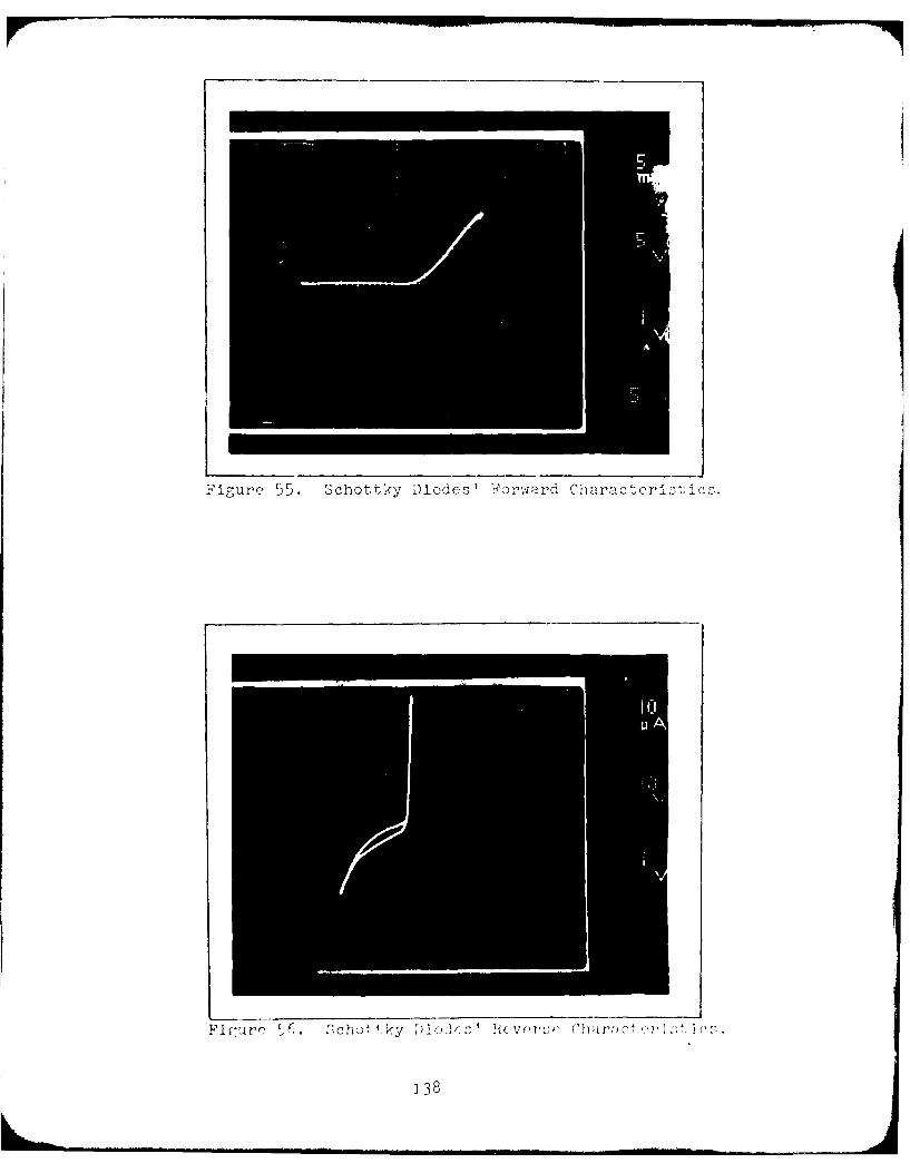
Figure 55. Schottky Diodes' Forward Characteristics.
Fl pur? . ,chot tky D iol.s hcvnrs, C'bir: c, : 3 a
138
APPENDIX B
THE SINGER AUTOMATTC INTEGRATED CIRCUIT
TEST SYSTEM
139

APPENDIX B
THE SINGER AUTOMATIC TINT F C RATED CIRCTJT
TEST SYSTEM
Description
The Automated Integrated Circuit Test System is capable of
performing full DC parametric testing, data logging, data
plotting, and data analysis on itnegrated circuits (Ref 21).
The system may be used to test circuits at the wafer level
using a TAC (Transistor Automation Corporation) Automated
Probe Unit (Figure 65). Discrete components can be tested
on the system as well.
The primary function of the system is to test the DC
parameters of a device or devices. DC parametric testing is
defined as measuring IC voltages, currents, and values of
IC resistors at high accuracy and at low stimulus test
frequencies under program control.
A Varian Omnitask Minicomputer utilizing 32K core of
memory controls voltage and current source supplies, necessary
peripherals, a digital voltmeter, and the TAC probe mentioned
above. In addition, via an instrument control board, the
Varian selects the individual supplies and voltmeter using
a complex matrix system as shown in Figure 57.
A block diagram of the entire system is shown 4n Figure
58. A photograph and drawing of the Singer system are
shown in Figures 59 and 60.
Test System Subsystems
The Singer test system consi;ts of several subsyr!,ms
which together provide the capability of forcing voltages and
1 40
L- II11I I

_ _~~ ~~~ _ _ _ _ _ _ 1 7-
_ _ _ __ _ _ - o
_ _ _ _ _ _ _ _ -co
-KE
I-- _ _ _ _ -_ _ _ _ _ _ _ - en
Ln
U)

LUj
-j L- 1.LU ><
(I)::: - ~- L
Cif- CL
LAJ~- C: -r
C-) C -
CD CDCQ)~
CL E
C.)*
1.0 4- 1-,
cl:i
L'ci
C) ~ ci
LV)
S.-
L-
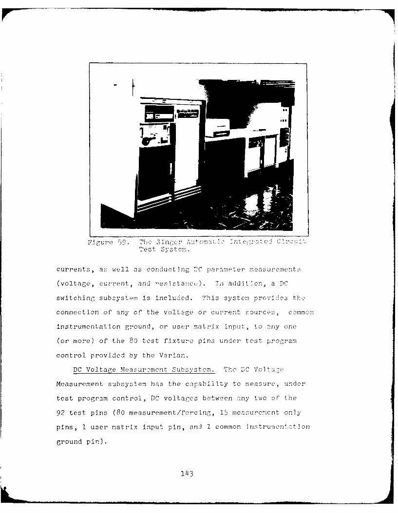
Figure 59. The Slnet ' c .. neC.uiTest System.
currents, as well as conducting DC paranmeter measurements
(voltage, current, and reslstanct). In addition, a DC
switching subsystem is included. This system provides the
connection of any of the voltage or current sources, common
instrumentation ground, or user matrix input, to any one
(or more) of the 80 test fixture pins under test program
control provided by the Varian.
DC Voltage Measurement Subsystem. The DC Voltace
Measurement subsystem has the capability to measure, under
test program control, DC voltages between any two of the
92 test pins (80 measurement/forcing, 15 measurement only
pins, 1 user matrix input pin, and 1 common instrumentation
ground pin).
1.43

cl.L~ : -
02
LUj
(2 H____m _j
- C)
CD L~UCD
__________________ _________ __________________CD
Of C)
CC-) <) C
0
C))
<w
0
LL-J
CU LU - ;7f
c:71 :D1

The DC voltae measurement capability is as follows:
A. Ran-cs: + 100mV full ,caje to + 200V full scale
B. Resolution: + 0.001 , of rangeC. Accuracy: + 0.01" of the absolute TC voltage resent
at the test pin.
D. Input Impedance: at least 10 mego l ms on all rances
DC Curr-ent e ... ubsvtems The DC Current
Measuremnt subsystem has the capability to measure, und-r
test program control, DC currents drawn by a device (transist-Lor,
resistor, diode) connected between any two of the test Pns
of the matrix.
The DC current measurement capability Ls as follows:
A. Range: 0 to 1.0 ampere.
B. Current Measurement Accuracy: + 1 of actual value.
C. Current Limit Range: 0 to 1.1 amp.-3
D. Current Limit Resolution: IRANGE x 10 amps.
2
DC Resistance Measurement Subsystem. The DC Resistance
Measurement Subsystem has the capability to measure, under
test program control, the DC resistance of an integrated
circuit or discrete resistor connected between any two pins
of the matrix.
The DC Resistance measurement capability is as follows:
A. Ranges: 10.0 ohms full scale to 200k ohms full scale.
B. Resolution: + 0.001% of the range
C. Accuracy: + 0.04% of the absolute resistance between
the two test pins being measured.
Th2 subsystem uses Kelvin wiring and switching techniques
1~45

in order to provide accurate and repeatable resistance
measurcments. In aiddition, the subsystem uses a 4 te2rminal
type of measurement which consists of two DC voltage sense
lines and two ohms "signol" lines.
The subsystem is thus confiurcd by using one of two
constant current prog'rammable power sup!lies contained in
the test system as the ohms "signal" lines, measuringz the
voltage across the res-'istor under test with the DC voltage
measure7mnts ubsyste: and using the System controller to
calculate the resist- nce in ohms.
DC Stilmr clu: isr:stem. The DC stimulus subsystem
provides five pr, :mble volta co sources (VSl-VS5) and
two pro2-na > ' -tant current sources (CSI and C'72)
as shown in 7i-u and 58. Bach source is independently
programma's C in varlous : lodes of operation which will be
described T-n tY.e follow'in.g paracraphs. Each source has
internal over-volt ce and over-current protection and makes
use of a floating Kelvin type of output which consists of
analog high, analog laws, sense high, and sense low.
Each source reduces digital noise on the analog output
using isolated control logic. Additionally, each source
contains its own internal memory which acts as a storage
buffer for programming data. The output of each source
remains constant until a change is initiated by the Test
System Controller.
146

The programmable power supplies, VSI, VS2, and VS3 hive
the following spedifications:
A. Output Voltage: 0 to 4 ]6.0V in 1.OmV inerement:;
B. Output Current: 0 to + 100mA, Short-circu1t rprotected
C. Current sink capability: + 50mA, overload protected
D. Accuracy: 0.01/ of the progras.med value (which depend::
on the condition of the power supplie."
due to calibration inaccuracies or corponent
failure in the sources themselves.
E. Load regulation: 0.001%
F. Line regulation: 0.001% for a + 10" change in line
voltage.
The programmable voltage power supply, VS 11, is a volta,'e
forcing-current measuring DC source with the following speci-
fications:
A. Output voltage ranges: 0 to + 32.0V full range:
0 to + 9.OV in 1.0mV increments:
And + 8.0 to 32.OV in 4.0mV
increments.
B. Output voltage accuracy of programmed value:
+ 0.5% of the full scale voltage range.
C. Output Current range: 0 to + 100mA minimum.
D. Current measurement ranges and resolution r-.quirements:
FULL SCALEMEASUREMENT RANGES RESOLUTIOn!
0 to + 4.OvA + lnA0 to ; 32.OiA + lOnA0 to T 250pA + ]00nA0 to T 2.OmA l ]pAo to ; 16.omA + 10A0 to T l00.OmA T 10011A
147

E. Current measurement accuracy: + 1.0/ of the actual value.
F. Current limit: + 110.0" of the full scale current
measurement range.
VS5 is a programmable voltage power supply and it functions
as a voltage forcing-current measuring unit with the following
designed specification:
A. Output voltage ranges: 0 to + 16.0V full range;
0 to + 9.0 volts in 1.0mV increments; and + 8.0 to
+ 16.0 volts in 4.0 mV increments.
B. Output voltage accuracy of programmed value: + 0.25
of full scale voltage range.
C. Output current range: 0 to + 1.0 Ampere, minimum.
D. Current measurement capability: 0 to + 1.0 Ampere.
E. Current measurement accuracy: + 2.0P of the actual
value.
F. Current limit: + 110% of the full scale current
measurement range.
CSI is a programmable constant current source and functions
as a current forcing-voltage measuring unit with the following
specifications:
A. Constant current output (Programmable):
FULL SCALE RANGES RESOLUTION
0 to + 500nA + 100 pA
0 to + 5pA + 1 nA
0 to + 32jjA + 5 nA
0 to + 250vA + 50 nA
0 to +2 mA + IpA
0 to + 16mA + 31jA
0 to + 100mA + 20pA
148

B. Programmed accuracy of the programmed constant current
value: + 1% of the programmed value.
C. Voltage measurement accuracy: + 2.0% of the actual
value, from 0 to + 32.0 volts DC.
D. Voltage out-put range: 0 to + 35 volts minimum (110%
of the full scale voltage measurement range) with a
programmable clamp voltage of l.OV increments minimum.
CS2 is a programmable constant current source that functions
as a current forcing-voltage measuring unit with the following
specifications:
A. Constant current output (programmable):
FULL SCALE RAU1ES RESOLUTION
0 to + 250oA + 40 nA
0 to + 2 mA + 250 nA
0 to + 15 mA + 2 -WA
0 to + 100 mA + 15 PA
B. Programmed accuracy of the programmed constant current
value: + 1% of the programmed value.
C. Voltage measurement accuracy: + 0.2% of the actual
value from 0 to + 100 volts DC.
D. Voltage output range: 0 to + 110 volts, minimum
(110% of the full scale voltage measurement range)
with a programmable clamp of l.OV increments minimum.
1 4 9

System Test FI xture/Performance Board
The System Test Fixture/Performance Board is defined as
the unit which interfaces a device (integrated circuit (S!T)
elements such as transistors, resistors, and diodes, discrete
transistors and resistors and discrete diodcas) under test
and its associated "performance. circuits," to all measurement
and stimulus subsystems contained in the test system. A
performance circuit is defined, according to the reference
used, on a per pin basis, as a
"Special circuit, such as a passive load, an active
load, a capacitive load, or a special interface circuit,
which is connected to some pins of the device to allow
stimulation of realistic device operation conditions
during the test procedure." (Ref 21).
DC Switching Subsystem
An 11 x 80 (Kelvin (2 wire) high reliability shielded
mercury wetted and dry reed relay matrix is provided which
allows the Kelvin connection of any of the sources (VS]. throuch
VS5, CSl and C02), the common instrumentation ground, or the one
user matrix input, to any (or more) of the 80 test fixture
pins under test program control (Refer to Figure 57).
Each reed relay pair (Kelvin matrix crosspoint) in the
matrix has independent storage capability. Independent, storaf-e
is the ability to remain in one of two switched states; (after
initial programmed switching by the test system controller) without
the need for further holding commands from the test sy.stem controller.
A master matrix clear line Is provided that will disc.onrioct all
inputs to the 80 pins of the test fixture under progi-i control.
150

All cabling connections are made of high quality shielded
cable with shield grounding techniques used so that system ground-
loops are minimized.
A shielded, 92 input (minimum) 2 wire reed irelay matrix is
provided which allows the two inputs (high and low) of the
DC Voltage Measurement Unit to be switched under test progr'am
control, to any two of the 92 test pins.
Close Relay Matrix/7xternal Instrument !ultiplexer
A special relay network is provided so that any one of
the instrumetns (Vsl-VS5 or CS]. and CS2) can be replaced
by an external instrument under program control as shown in
Figure 57. The matrix is designed so that either, but not both,
VSI or External A device may be closed to the main switchirn
matrix which applies to all instruments except for the DVM bus.
The external devices can be alternate power supplies that remin
at a voltage or current value determined by the prograTmer and
are not programmed by the programming language. The Close
Relay Matrix and associated matrix sections will be discussed
further in Appendix D.
Instrument Control. System
The Varian Computer transmits signals to the buffered ]/0
controller located in the I/O Expansion Chassis which are in turn
sent to the Instrument Control rack to control the entire system.
The Instrument Control rack contains receivers, decoders, and
timing circuits to control the 7 power supply instruments, close
relay matrix box, 16 external relay drivers avallaible at the relay
motherboard, and the analog-to-digital (A/D) converter Includin7,
the ranging control on the A/D input amplifier.
151

Test System Controller
The user programmed Test System Controller controls all
programmable elements contained in the test system with the
following characteristics:
A. Memory capacity: supplied with 32K works within the
mainframe.
B. Memory cycle time: 1 ]isec or less.
C. Word length: 16 bits.
D. Memory addressing: direct.
E. Supplied with a ROM bootstrap loader.
F. Input/Output channels: Two input/output channels are
provided to allow for user installed test instrumentation
to interface to the test system controller. Each I/0
channel has the capability to input 16 bits and
output 16 bits under test program control via plug-in
interface cards. This enables the ability expand the
the capability and reconfiguration of the test system.
G. Controller memory has the ability to retain stored
information for one week without test system power.
H. A Direct Memory Access Channel (DMAC) is used with the
dual magnetic disc unit.
I. Necessary time delays required for proper operation
of all test system instrumentation can be generated
under test program control.
152

_w
The Test System Controller constL; of the VAiIIAN 620/f-i00
minicomputer, 32K memory expansion unit, and an I/0 expansion
chassis.
System Controller Peripherals
The System Controller peripherals are shown in Figure on
the far left side.
Keyboard Entry and Information Printout Unit. A Texas
Instruments Silent 700 table-top high speed teleprinter is used
to input programs required for real-time testing. The teleprinter
has the capability to transmit and receive data from the test
system controller at speeds up to 300 words per minute or 30 cps.
The unit is sued as the main I/O unit for the controller.
High Seed Paper Tape feader/Punch Combination. The test
system is supplied with an optical 300 cps paper tpae reader/
punch combination with the capability to operate in the step or
continuous mode. The reader uses an 8-level code while the punch
is capable of punching 75 characters per second and has the
ability to duplicate the tape being read by the reader.
Magnetic Disc Unit. The test system uses a moving head dual
magnetic disc driver unit (PERTHC 3000) which uses two upper and
lower disc cartridges. The lower disk is permanently installed
with the disk driver unit itself and is used to store th, operating
system software for the computer. The upper disk is a re:rovable
hard pack used to store all user programs. The total storage
capability is at least 2 million 16 bit words.
153

Information Display T,'rmini. A Tektroni.x Model 11012-1
Display Terminal (hard copy compatible) is supplied with the
test system. The unit allows input and output of alphanumeric
data and the output of graphic data at an input/output data rate
of 9600 bits/sec. The display terminal use is that of scheduling
DC parameter test runs, calibration runs, the assignment of logical
unit names to the peripehrals, and providing the user (or programmer)
the ability to communicate with the operating system.
Information Display Terminal Hard Cony Unit. A Tektronix
Model 4610 hard copy unit is connected to the display terminal.
The hard copy unit produces permanent high-resolution, dry copies
from the display terminal.
Magnetic Tape Unit. A WAINGCO Model 10, 7 track magnetic tape
unit, is supplied with the system. The tape unit it IBM compatible
and has a data density of 556 (HI)/200(LO CPT).
Line Printer. The Data Products Model 2410 Line Printer
(not shown in Figure 58), but connected to the I/O Expansion
Chassis) is sued to output source programs as well as data.
Speeds ranging rrom 245 lines per minute, and 132 columns, to
1110 lines per minute, and 24 columns of printed characters from
a 6 4 -character set are possible.
TAC Probe and Controller. The TAC Probe iCI atroller are
discussed in Appendices C and G.
154

APPENDIX C
TEST SYSTEM SOFTWIARE
155
APPENDIX C
TEST S YSTE'., SOETWAEE
Test System Software Package
The test system is furnished with a software package to
permit the user or programmer to write test programs. The
system monitor program controls the overall software operation
of the test system which initiates all input, output, data
analysis, and control of the test system during system operation
(hef 21). A simple, English-like test oriented language called
Elucidate, is the programming language for the system and will
be described later in this Appendix.
Compiler. On-line program translation is supplied with the
test system by the software package. A disc resident compiler
configured to match the system hardware comprises the software
package. The compiler operates in the batch processing mode
in conjunction with the Source Editor for corrections. A start
execution, RUN, executes the test program after it has been
compiled and all diagnostic errors removed.
Editor. In addition, on on-line test program editing
capability is provided. The on-line test program editor allows
the programmer to change or add instructions or test sequences,
and delete instructions or test sequences via the teleprinter
keyboard.
VORTEX Operating System. An on-line magnetic disc operating
system is also included in the software package. The disc
operating system, known as VORTEX (Varian Omnitask Real-Time
Executive) is capable of:
156

A. Loading the configured test system software into core
memory from the disc.
B. Storing test programs written in the Elucidate test
language onto the disc.
C. Loading test programs from the disc into core under
operator and test program control.
D. Executing test programs under operator control.
E. Deleting test programs on disc.
F. Repacking the disc.
G. Storing and recovering test data under control of
a test program.
H. Linking test programs in order for a new program to be
loaded from the disc under control of a resident test
program and automatically executed. This new program
replaces the requesting program in core.
I. Storing, recovering, and executing machine object
code resulting from compilation of FORTEAN and assembly
language programs.
J. Storing, recovering, and executing utility programs.
Available Programming Lan~ua-es. In addition to the
Elucidate test language, FOTTAN IV and assembly languages are
supplied to allow for user data processing. The user is also
capable to write assembly language programs for any additionally
installed instrumentation.
Software Drivers. Software drivers are supplied for all
test system instrumentation, including Automation Corporation
Automatic probe unit. The software driver for the TAC probe
controller enables a test program to completely control the
157

TAC probe unit (See Figure 6'' , Appendix G) The followinc items
are controlled by the software driver under test program control:
A. Sense the up or down position of the z-staoe.
B. Move the z-stage to the up or down position.
C. Control the in-place inker on the probe unit.
D. Tnitiate an independent or simulataneous X and Y indix
operat ion.
E. Control independently the X and Y step size.
F. Sense the completion of an index operat)ion.
G. Sense the Start Test signal from the probe controller.
H. Sense the Emergency Stop si-nal line from the probe
controller and create a priority interrupt to the test
system controller if an Emergency Stop condition occurs.
Graphics. The Advanced Plot-la Tektronix software package
is supplied with the display terminal to provide a graphics
capability for the system.
Elucidate Programminc Test Languae Description
The Varian 620/f-l00 computer controls a real-time test
situation and requires certain specialized logic elements (Ref 22).
The Elucidate programming language combined with the logic
elements of the Singer test system provides the computer with an
error free test device. A 16-bit binary data word transferred
from the computer to the test system (power supplies, digital
voltmeter, etc) is the basic element of the Elucidate control
system. The test system uses a three dimensional array concept
of X, Y, and Z addressing. This allows the Elucidate programming
language to define the necessary control functions to the test
system. To accomplish this, the 16-bit binary word is divided
158

into four elements. The firsl element i a 1-bit word which
separates test sys-em com-,monds andl c omtp iit r c onto1o
Element two is a s-bit "VERB." field used to define an action
which the test sys tem must perform. A typical verb Is "SET
which is used in an instruction such as
SET VSI 4.5V3 10.011A
where "SET" sets the voltage output of power supply VS at
4.5V and at a maximum limit or clamp current of 19.0.A. A
maximum of 31 verbs is provided by the Elucidate languase.
The third element is a 5-bit "NOUN" field which is defineo az
the place where an action occurs. A typical noun in "VSI" as
in the above command. The fourth el-ement is the "MODIFIER"
which consists of 5-hits which are used to describe thc test
point locations. A modifier can be an integer or real number,
unit of measure, or a variable. In the case of the above command,
4.5 and 10.0 are real numbers, whereas V(volts) and .A(milliam:::)
are units of measure. One 16-bit word is not adequate t,-
describe the required conditions for certain actions .:hch the
test set performs. A multiple word command is used in this
case with the first word containing VERB, N[OUN, and MODIFIER,
and the following words specifying additional conditions in
a predetermined fnrmat. The above command is such an example.
The modifier "10. " is an additional condition specifying that
a circviLt installed in the test system can draw a maximum
current of about 10.0mA from VS1.
159

The thrcs.-d mensional address location can describe any
function required of' the test system. Each function, therefore,
normally has a three input gate that consists of a VERB, NOU',
and MODIFIER. With all three inputs true, that function and only
that function will activate. The Elucidate language easib:l has
control of this complex system using this addressin- scheme.
The Elucidate Compiler transforms English com!:nands and
numeric locations to the 16-bit data words comprehensible by
the test system. The compiler is written in DAP MR MACRO
assembly language with access to the compiler gzained through the
Test Set Operating System (TSOS) which is then accessed by the
Varian's VORTEX operating system.
From the previous discussion, Elucidate is a unique test
language. It is a simple language, but it is necessary to
describe it further to understand the YESFET orogram.
After the items in the previous section were determined, the
power supplies were rcquired to be initialized using the
following commands as an example:
100 :CONDITION TEST SYSTEM FOR TESTING
110 RESET
120 ENABLE VSl: VS2;VS5
130 CLOSE GND; VSl;VS2 ;VS5
140 CON GND 40; VSl 41; VS2 36; VS5 48
The RESET command initialized the matrix system (removed
power supplies, voltmeter, et cetera from the matrix). In other
words, it caused the test system to be reset to a neutral
condition with all previous commands negated. After every RESET,
the remaining commands were required. The ENABLE command
160

signalled the power supplies to switch to thje on state. The
CLOSE command provided the capability to pre-estabiish the power
supplies and "round (OND) selected prior to the connection of
the test point matrix pins. The CON (CONN7ECT) command connected
the power supplies and GND to the individual test point matrix
pins. A DIS (DISCONNECT) negates the CON command. From this
point on, the power supplies had to be set at the desired voltage
and current clamp value using the following command:
150 SET VS5 5.OV, 20.0MA
The SET command sets VS5 to 5.OV at the maximum allowable clamps
current drawn by a device at 20.0MA. To measure this voltage,
the voltmeter must be connected using
160 CON VMH 48; VML 410
The CON command connects the voltmeter between pins 48 and
40. VS5 is also connected at pin 48 and GND at 40. Therefore,
when the command
170 READ VMH 4
is reached, the voltmeter is read at approximate]y 5.0V
(+ 0.01% of the absolute DC voltage present at the t-st pin).
The above command not only caused a measurement to be taken,
but stored the measurement with the line number as a reference
location for the data obtained. In addV' :on, the interer 4 or4
MOD number was specified with 2 or. 16 measurements actually
taken and averaged. A print command using the line number
location of the measuremenL caused the voltage measurement
obtained to be printed with the unit V or volts.
Current measurements were made using the following command:
180 READ VS5 4
ll

Current was measured and averaged as before with a rint
command (not shown) printing the current in A or amperes.
Appropriate conversion to MA was obtained by multiplying the
results at line 180 by 1000.0 and substituting PIA for A using
formatting.
Call to subroutines are made using the following command:
190 GOSUB 1330: CALL PINCH-OFF VOLTAGE (UP) SUBROUTINIE
The subroutine was called to an ENITER statement located at
line 1330. A GOTO statement placed before entering the sub-
routine was then necessary to prevent accidental entry to the
subroutine (not shown). The GOTO statement, when reached,
skips the entire subroutine and continues with the next state-
ment. A RETURN command returned control to the main program.
All results obtained in the subroutine were automatically
carried to the main program and remained the same until the
subroutine was entered again.
Variables were used throughout the program using only
Elucidate variables, ZA, ZB,.. .ZZ. Measurements taken were
set equal to variables using the command,
200 EQ, ZA, 180
where ZA was set equal to the measurements taken at line 180.
To set a variable to an integer or real number, the command
210 EQ, ZA, 250.0
had to be used to distinguish the difference between a line
number and, an integer or real number.
Simple algebraic manipulations could also bc performed
(multiply, add, divide, subtract). These commands an] their
162

variations are shown below as an example:
220 MUL,170,1.0
230 DIV,]70,180
2410 SUB,170,ZA
250 EQ,ZB,7.0
260 ADD,170,ZB
At line 220, using the previous commands presented at their
respective line numbers, the voltage reading is multiplied by
1.0 and the result stored at line 170. At line 230, line 170 is
divided by the current reading at line 180 with the result
stored at line 150. Afterward, line 170 is subtracted by ZA =
250.0 with the result stored at line 170. The variable ZB is
set equal to 7.0 and then added to the result at line 170 with
the final result stored at line 170.
163
- i i i | . . . . .- _• .. .

APPENDIX D
MATRIX CONTROL OF THE TEST SYSTEM
164

APPENDIX D
MATRIX CONTROL OF THE TEST SYSTE'll
Figure 57 of Appendix B is a basic diagram of the Elucidate
controlled system (Ref 22). The output of the test system at
any test point is subject to a selection of switches. The
instruments or power supplies are connected to the voltmeter
via the proper switch. These switches or relays are controlled
by the compiler which allows only those commands that are
technically feasible. Other checks are made to safeguard the
hardware.
Five test equipment (matrix) control verbs are provided:
CLOSE, OPEN, CONNECT, DISCONNECT, and RESET. CLOSE provides
the capability to pre--establish the instrument selected prior
to connecting the test point matrix to the instrument. The
OPEN command negates the CLOSE command.
The verb CONNECT and its negative, DISCONNECT, are used to
connect/disconnect individual test points to various instruments.
The verb RESET returns all relays to their DISCONNECTED,
OPEN state and does not have nouns associated with it.
In order to prevent undesirable combinations of switchinc,
the following rules presented in the programming manual (Ref 22)
were established for the system:
A. All nouns (or instruments), except the voltmeter
(VMH, VML) and resistance measurement instrument
(RMH, RML), must be CLOSED before being CONNECTE.D.
B. The voltage and current supply nouns (VSl-V.1,, CSl and
CS2) may not be closed with their respective externals.
165
For example, VSI may not be closed with External A
instrument at any matrix switching connection or pin.
C. Each noun is classified as a forcing type of sensing
(measuring) type.
D. Forcing nouns (power supplies) can be connected to as
many pins (testpoints) as desired; however, no
two forcing nouns may be connected to one pin at the
same time.
E. Sensing nouns (voltmeter) can be connected to only one
pin at a time; however, there is no restriction as
to cross connection of these nouns.
F. Since the voltmeter is differential (described by two
nouns, Voltmeter Measure High (VMH) and Voltmeter
Measure Low (VML), both VMH and VML must be connected
before the voltmeter is read. This holds true for
Resistance Measure High and Low (RMH and RML).
Table XI shows the interrelation of Elucidate verbs and
nouns by indicating their allowable and required combinations.
166

TABLE XI
VERB/NOUN APPLICABILITY TABL-E--MATRIX CONTROL VERBS
VER BS
NOUNS CLOSE OPEN CONNECT DISCONNECT RESET READ P
VS1 X X X X X
VS2 X X X X X
VS3 X X X X
v514 X X X X X X
CS1 X X X X X X
CS2 X X X X X X
EXT A X X X X
EXT B X X X X
EXT C X X X X
EXT D X X X X
EXT E X X X X
EXTE F X X xX
UP X X X X X
VMH X X X
VML X X X
RMH X X X X X
RML X X X X
RELAY X X
GND X X X x ____I___ ___
167

APPENDIX E
VARAiNi 620/f-100 COMPUTER CH-ARACTERISTICS
168
APPENDIX E
VARIAN 620/f-Ie CO?.PUER CI ARACTR!KITICS
Varian 620/6-200 Features
The Varian 620/f-100 computer (Ref 23) is a high-speed,
general purpose, digital computer for scientific and industrial
applications is shown in Figure 61 and has the following features:
Memory cycle time: 750 nsec.
Instruction set size: 142 plus 8 optional instructions.
Word length: 16 bits.
Modular core memory: Expandable to 32,768 words in 4.096 or
8,192-word increments.
Automatic data transfer: Direct memory access (DMA) with trans-
fer data rates to 275,000 words per second; priority memory
access (PMA) for transfer rates to 1.3 million words per second.
I/O capability: 61 devices can be placed on the I/O bus with
the I/O system expandable to include automatic block transfer,
multi-level priority interrupt, and cycle-stealing transfers.
Software capability: DAS 4A,DAS8A, and DAS MR (MACRO) assemblers;
binary load/dump (BLD II): debugging (AID II); computer
diagnostics (MAINTAIN IT); mathematical subroutines; real-time
monitor (RTM), source program editor (EDIT); master operating
system (MOS) for fixed-and moving-head discs, drum, and magnetic
tape; ANSI FORTRAN IV, conversational BASIC; report generator,
RPG IV: and an extensive library of programs in the Voice
user's group.
169

r
@varian data machines 620/f
Figure 61. The Varian 620/f-l00 Computer.
170

In addition to the software capability, the Varian compiles
Elucidate source code and ther converts it into machine lanr-uage
object code using the DAS MR (MAChO) assembler.
Functional Oranization. The Varian 620/f-l00 computer
functional organization is shown in Figure 62. Further infor-
mation concerning the detailed operation and organization of
the 620/f-100 computer is beyond the scope of this thesis.
Therefore, the reader is referred to Reference 23.
171

Z
Ii " I C.)
CC
2, 0
_ . _ _ I _______ _]
I. i I --
o~Io I;
aS ' I
]72~

AD-AIO0 762 AIR FORCE INST OF TECH WRIGHT-PATTERSON AFB OH SCHOO-ETC PLD 2THE AUTOMATED DC PARAMETER TESTING OF GAAS MESFETS USING THE SI--ETC(U)SEP 80 T L HARPER
UNCLASSIFIED AFIT/IEE/GE/80-7 ML
lllllmhhhhhhhhmmmhlm

APPENDIX F
VORTEX OPERATING SYSTEM
173

APPENDIX F
VORTEX OPERA71 '-!'A
The Varian Omnitask Real-Time Executive (VORTEX) (Ref 211)
is a modular software operation system for controlling,
scheduling, and monitoring tasks In a real-time multiproramming
environment. VORTEX provides for background operations such
as compilation, assembly, debugging, or execution of tasks not
associated with the real-time functions of the system.
VORTEX is comprised of the following basic features:
-Real-time !/0 processing
-Provision for directly connected interrupts
-Interrupt processing
-Multiprogramming of real-time and background
-Priority task scheduling tasks
-Load and go (Automatic)
-Centralized and device-independent 1/0 system using
logical unit and file names
-Operator communications
-Background programming aids:
FORTRAN and RPG IV compilers, DAS MR assembler, load-
module generator, library updating, debugging, and
source editor
-Use of background area when required by foreground tasks
-Disk/drum directories and references
-System generator
174

SystL m Flow and Or'F;ani-sation
VORTEX executes foreground and back,:,round tasks scheduled
by operator reouests, interrupts, or other tasks. All tasks
are scheduled, activated, and exceuted by the real-time
executive component on a priority basis. in the VORTEX Ioperating system, each task has a level of priority that
determines what will be executed first when two or more tasks
come up for execution simultaneously.
The job-control processor component of the VORTEX system
manages requests for the scheduling of background tasks.
Upon completion of a task, control returns to the real-time
executive. For a background task, thre real-time executive
schedules the job-control processor to determine if there are
any further background tasks for execution. During execution,
any foreground task can use any real-time executive service.
Important foreground and background tasks are defined
below:
Foreground Tasks:
Real-Time Executive (RTE): Processes, upon request by
task operations that the task itself cannot perform.
Inpbt/Output Control (IOC): Processes all requests for
I/0 to be performed on peripheral devices.
Background Tasks:
Job-Control Processor (JCP): Permits the scheduling of
VORTEX system or user tasks for background execution.
Positions devices to required files, and makes
logical-unit and I/O-device assignments.
*1 7 L

File-Maintenance Component (FMAIN):
Manages file-name directories and the space allo-
cations of the files. It is scheduled by the JCP
upon input of the JCP directive,/FMAIN.
176

APPENDTX G
PROBE CARD DEVELOPMENT AND THE
TAC PROBE UNIT
177

APPENDIX 0
PROBE CARD DEVE'LOP 'M1.NT AND T"147 TAC PRODE UNIT
A probe card was developed by AFAL to provide an interface
between the Singer and the NAND/NOR logic circuit chip shown
again in Figure 63. Thc probe card is shown in Figure 64 under
development in the probe card station. A probe is soldered
on the probe card corresponding to the contact pad position on
the logic gate. The tip of each probe is about 1 mil in diameter
and is to make contact with the corresponding pad of the NAND/
NOR MESFET circuit of Figures 1 and 2.
The contact pads on the chip of Figure 63 correspond to
the connections for the power supply voltages, input/output,
and ground provided by the Singer system. Each pad is numbered
to correspond with the Singer's matrix pins (Figure 57) of
the system performance board. The correspondence of each pad's
function with the necessary connections is shown in Table XII.
Interface between uhe performance beard and the probe card
is provided by low resistive colored ribbon wire and an edge
connector receptacle. The probe card is slid into the
receptable and in turn is attached to the TAC probe mount as
shown in Figure 65.
178

> < Ur)
1- 000- H
Ld' 0
~ Ito~to
uj iLV)LLU
- z']00 0 ~~.
F- 0 0
0 0 ILi.
m-
LLL0
1179

0) 0 H C)
0
0 0D LlwP0 0
E-4 0 - 0 0 0 C) U) CIO :2 0 0 0
0- E-4 0 0 o oC) 0 A I-I0 0 0 0 0 -I -
C) H-E-A0 0 i)~ - -
co 0l - D H-- H H- 0OH L4 0 0) 0/ V) Q 0- 0
c) c
wA 0
"0 0- ~ 0 0 0 1 0 04 D~~' '
,0i 00>
o l
HA
HAA
:V0 04 ~- 0)0 H N (N -) 0-7 0- \ r 0 C
HA180

(a)

7,1w
d ('inV


APPENDIX N
REQUIRED PROCEDURES TO FEEFORM AUTOlTE.7D
TESTING USING TEIE MESFE.T PROGRAM
183

APPETNDT X !!
R R Q U T rT iE P ! , O C E P 'J Y,' . , AI S' . .., 'T ..: 2. 2 _ _ _ _ _£ .. ... ...
PR 0 R AM
In this appendlix, detailed procedurcs will be presented in
order to nerform automated test in7 usin, the ME3?F? pro-r:un.
The order of presentation is as folows:
1. Test System Preparation.
2. IESFEl Prorr1Sam TTsac-c.
3. M1,-SFPT Program Problems.
The programmer xs required to understand ti 1i procedues -I
order to run the [,ESFET program successfully. It should be
understood that the MESFET program ha's niot been fully develosod
due to equipment comolications. Areas in the program ',hat .,,
require further investigation will be pointed out. This will
reduce any problems that may occur :in using the 7.MESFET p rogran
to perform automated testing of the GaAs MESFET NAN D/NOR. logic
circuit.
Test System Preprration
In this section, it is assumed that the power supplies,
Varian computer, and all peripherals have been turned on prior
to performing automated testing. It is also assumed that the
power supplies have had at least one hour of warm-up time. Test
system preparation will now involve the following (Refer to
Figure 66):
1. Load VORTEX operating system into main core memory from
the disc using the following:
184

a. Clear all re:-isters. (Load 0 000 000 000 000 000).
b. Load 0 000 000 000 000 001 into the A reegister.
c. Load 0 Ill 11 110 000 0O0 into the P recister.
d. Place V0oTEX Boot tape into paper tare/readei, punch.
Depress LOAD Switch.
e. Press the TNT (Interrupt) and Reset switches.
f. Place STEP/RUN switch in RUN position.
g. Press LOAD. The VORT,.X Boot tape will now run
through the paper tape reader and load the operatin-
system.
h. Loading of the operating system will be indicated
by the following address indicated on the register
display
0 Ill Iiill 10 Ill ill
i. If the above address is not displayed, the entire
process beginning at 'a' must be repeated.
2. Assignment of peripherals will involve determining
which peripherals will be used to provide the desired method of
I/0:
a. Insure that the CRT, teletype, and line printer arc
placed 'on-line'.
b. Insure that computer select switch located on back of
line printer is set at 'VAR' or Varian.
c. Type; IOLIST on the CRT. The output is as follows:
185

TE(03I) E.00TA(03{0) =cT-/2 '
TL( 02) I';TO(028) = TY-0TI(027) = TY//co(o26) = hc0ZE0(0241) =SE(023) = DAAPL(Ol6) = P voKED(0]5) = Tos(0l3) = D00,ES(0l4) = DO;JSI(002) = CT$O0SO(003) = CT00PI(004) = CR,0LO(005) = LrOBI(006) = PTO0BO(007) = PT 0ss(oo8) = D004GO(009) = DOOGPO(010) = D00MDI(011) = TYOODO(012) = TY0ZCU(101) = D V/_ -SW(102) = DerFCL(103) = DOOA0M(101) = DOODBL(105) = DOOCFL(106) = DOOB
d. If the magnetic tape unit is desired to be used to
store or output programs in conjunction with the teletype, type
the following on the CRT;
;ASSIGN,TL TYOO
;ASSIGN, ED = MTOO
e. If the magnetic tape unit is desired with the line
printer, type the following on the CRT;
;ASSIGN, TI, = LP0O
;ASSIGN, ED = MT4Q
f. To use the line printer in conjunction with the
teletype, type the following
;ASSTGN, TL = LF00
;ASSICN, ED = DU
186

g. To use the teletype a,- th( primary I/0 device, type
;ASSIGN, "LL = TYZ0
;ASSIGN, ED = DUl
The teletype can be used to input and store programs re-gardless
of the peripheral assignment. The primary method to input programs
is accomplished at procedure 'g'.
3. Scheduling of Tasks will be performed in order to calibrate
the test system automatically as well as to begin automated
testing:
a. To calibrate the system automatically, insure that
procedure '2.f'. is performed.
Then type
;SCHIED, CALIB, 2, FL, F
on the CRT. Afterward, refer to the teletype for further
instructions. CALIB will indicate the status of all power sup-
plies including sensitivity deviation, offset error, et cetera.
b. To set the system up to perform automated testing,
type the following on the CRT:
;SCHED, TEST, 2, FL, F
This completes the preparation of the Singer test system to
perform automated testing.
MESFET Program Usa e
MESFET program usage will consist of the necessary procedures
required to perform tests on the Singer. These procedures are:
a. Refer to Figure 66. Figure 66 indicates the input
commands to place into main memory from disc compile, edit, and
run the MESFET program.
187

BEGINAUTOMAl ED
TESTING
TYPE OLD, MESFET
3
LIST LIST YES TYPEYES
E41SFET PROGRAM OMPLET PROGRA' ELIST OR EL
YES NO
LIST DESIREDLINES BY TYPING
EL LINE #'s
-T-
+
YESANY CHANGES YES
? REFFR TO MAKEPROGRAMMING NEEDED CHANGES
MANUALNO TO USE EDITOR
J
YESOMPLETE PROGR4 ESIRE LISTING TYPE COM
I NO NO
TYPE COMN
Figure 66. MESFET Program Usage Flowchart.
168

AUSERR SE UPPOE
PROGRAMRTYPERGRA
REPOD WITHN
IDO FORWAFE
COOUTRPUTPERh IT
COPTRRESPONDS WITH
'IITIALIZEYP TAIADINU
XTNDYP POSITIONN
ID FOR WAFER3
FigureE RE6.ND Continued.
189PRB U~ ',T
Ii

4
TYPE IN
AUTO OR MANUAL
TAG PPO3E MOVESTYPEDYES AUTOXATI'CALLYAU 0 ACROSS WAFER AIND
YYES
WAFUTR ERND WIREAH C ON IY
ND CODUT STOP
LOCATIPR O DERSS
Figure 66.AK Contnued
190 JOESO

b. To store any changes made to the MESFET program
type the following:
REPLACE , MESFET
It should be noted that the VARIAN periodically runs into
overflow or loses the starting address of the prorram. This is
indicated by the bit overflow display on the VARTAIN or that the
address display is not lit at all. It is also indicated by
no response from the computer on the teletype when RETURN is
pressed. All changes made to the program may not be lost. If
the previous conditions occur, loading of the operating system
is required according to the previously established procedures.
Changes made to the program will most likely be kept in the
'scratch' portion of memory wheve all changes are made prior
to storing them on the disc. Generally, there is no need to
call the MESFET program to memory the above problems occur.
When calling up the MESFET procram, problems may occur,
however. These problems are indicated by the fact that the
program may not compile correctly as it did befere. Phis is
believed to occur when transferring the program from disc to
memory. The problem can be minimized by leaving the dfsc drive
and VARIAN on. The program can also be called from main memory
(scratch areas) after a period of disuse, but is best to compile
the program to determine if any errors do exist. Common errors
not noted in the programming mnnual are:
1. Duplication of lines of code.
3. Omission of code.
If these errors do occur, referral to a correct MEC.YET program
listing is suggested to remove the errors.
191

APPENDIX I
MESFET PROGRA14
192

': S" ' I,'e i; + J' -+, . t , + I ' T w ,
K ' vt, io
5G, f, T
I" ~~~~~~~~~~ T Tr t1AL/ l- l.LN1S STm
'.I L I.l li t 2 i II I . 1r4.L T- i ( I..SI. L, T'-f t ;L0
4:v; l ;I,+ ,Y-[.L1' :~I~v5 I-2O AT y ' 1. 4,-> -I'i " :Lt Ai.t+ s I-¢( T /, I F) Y S
AA T
* ,l .h-- Lit. LU ' I) . ,. .. t l11t . r. A0 Ck -r *
t i :
.. I P L IL EAS5
P'., Lt ' L k r It X Y S I
'., ,,~~ S Ai , ,:f[Ih tf, , ,..L) JI , T I& C W"., -OL I ,.i ,,
:>,'.-- I *t -1 ,p - tUel-, ir. ( /.s , j Yf) L)
b ..... l P i:. +' ,T i~:
",,'+l l L V i i ,'b : O Iil
r, P V 47
C'+t ( ' I ViH 47 V 'L 4
£, ,.;l 1 , h!: r/ . C~. ,, 1 r L. il hS !JP CL.-FuLLPi,-,ERf*-
S ,. .t* *'efrAbtJr4: IL, S**
i,. .1'
-SI. .., ,1 I 7 U..V w (.'iS , T.A) V 0 V 0A N
'-,, tIV L , t1
:~,V! 4 I LA L; 1,1t 93
1.93

• * :_ SuS 4(,7 Llh.
f. t.. 4
~' IL .
/, Ctr \.',.; ,
L t- -"7
, U.' 4k L .L I'iV L
!.,3 1! I -1 Vt u h
''.)! :
/' )L PFh t bl LV,
Li U i", L : C .L.'3 , (N'; Vo l ; ftk%..
71 ' **Cij ,K-~-I': 5LU . t;. LV Ah
i-i',, :
7 ''.. [ENNL, blr 240;L.Kl, {II [T,, ( ) ,,R ,j tF
"v191

.. ,,'.. : PrI . L:- -. (,b ,[
t,): gDF: V " 4,$ vr' L E
,,
{,. V{,;,- ( ; V, 5: I
* W-1 *'
v .. x ,. 2 '
-4 ;0: " ,z 4, '
., F- [i. 1 '
L,,b SJ~ bt: L ... LLi .! F' VUL 1 A(,,,Ivr . , UF1A
Z) U L, L L I I4I
Lb v${ V, b1 41
£ ,t, hLU5U J 4?,b , '-L,.L t- ]L .UUY4N V fULA rY)P Lb k~T)j,i .-
A:,u L( .L) '1 : V f & 3I -. l,' NO L,'l L.} .. I N,
li,,f-'t,~~~~ 4O U L-4( ; ,L T b Ct 8[Ij t, U iLr ;[,it: I iA fI N Lt
S :
b, D 6 4;1 L A,.t.. *,l" L ) ' V 0 LT9,
IOAO~~~~ ~ I ,,,i~ u.b ~ , Luk. L C R.E F: h T L Et. (.li L %7NI ,
|O~195

L L
I ,rI ' LT .'V ' . i "
II LL
t11. T
U L 6" 6
131
Il~ i*,,i,, -I J r (r f ,i Tr S. (Jf" A. LTIV. I pL i **
;lTb :
li t'
IL-l :
I k,.t1; 5 ba L 'L /. 1 ' rL.I k11 At ,,h r 'v'L Ij.L,t (L v) SUtt~LUI li~L
Il'~' :
1 ;,
196

t i.'
I L, I
L". L (_ r f) 1 i, I ,,T,, 'U"
A /)
3 ,A S Ll I-'
" 1 T * A k t t L t o - L )14;'J L+ I( , : ,{
1 '-,".,/ L,.!
I '.~ * ii . .
L A V C . L I L A8 F z, * -'.(. : *,b-
I ,t'. I C
* 1t.):" L.J,/Jd, ] ''
lz hk ', Vb'. , :**Fr SLIktL J[Pl(NS)*
1: ' i;(, 1/&u :W-, i, - Ii ~ttL. I',R .'LTLI, M'L L.'kLi) : (, IF N[],
3 P: ;Lr.AVL C g i~t's.l t~S I5;$ F I t , *d. . L. CLf'' A t).
'(,+ **LI.tS, L,- .'-5141NL kl) [I- i. (;,,,-L AT ,S:O'
197

I L L I
I,~~ ~ ~~ 11 ] - 'i) . V- L~ )
0. C,
',,,ibL iC-
1 1 -' 1 I / .I ':
I', / ± '~ 1 l' A / C.' I '.
I e.L L (L: I
I L 'I
It'J' P;,I '.I 17, < 7; 1/
E .I 7/- 2 ' l(,% :
LI V ,
it, : * * I i T) 4,. /,
ll 1 ",L I
17;'b~ ~ ~~~~~~7 55.,'./) :*l;'(I)._~ . ),
I 7/I ~ L J, t13H, b C
b , A Y -( ) S 1 tNL,
fl11 P ,
1 h4 I I"U. l'iO , I (,C,. O
I t b L A I 1 .¢ )4) , 1 7 :
I h
195

I I # / ') i' i, !t I L
J' .1 :
. i, r~fj~ :< v<f* Li > Lk l G ': >
1V-', 1, :
:
. . r , U t
(I "! *l I~ L ' LL I r. j : r J
21.
717t. >>> > >h, /,LuI .
*Ui-( I L T L A t4 P t
2 3 i211 I ,N) 'o l, '17.l 1 .'o
217', :
2. I < :<< , Li (+0, A T luN>>>>>
199

C~ -,
2 *. 'l .U~ ~wi
2b<
t,, (. :
2, , t, T
e,4 t A!, (1 ~ ,l ,, - I I 0S, AS Io- I I L11
2.r, U 4 '1 ASw I FI*>>7->
2 4.
2 P C 2 .C; ~
2 ; A 4 r L 4, 0 Z, 0;..
2 '
2
2,,. -, :.iF 5,] V# AS, L-.U V, : I*,[, I Tc t:Uf),.ri , ~ A, I St- ,C;. IL 1'.i"
p t.. , I,- 3, \',; T U:;: --_1 ; YET , 0 V C '_) *& 2 [ 4 / ,
2~", 4 < < < C Ti i L .; F T. I S> .t , >t, >r' i L F ik;5i*
2 -' > - Li 1POO
/'5 3. b (',2L3j.
~~22O

; h,".t, ~~ i.,* - +J, :- V ,ll I C e.,i- V ) C I r, LT L L t I.* ** t mv I _s=_
257t :
S1 !t "7~
iit),j1L W +( :*,f T ' U U NAI, P' rd kf,.
2r ;L I
2r ; ) :
2tr,.,;2 ' , . Mi S ,NI 10 .e
A vo
K~ 0 1$ u , ('L5 iI I L TI
t "C N
F I it~ L~ I~ t,,f
SV T v -S5 5.Cv, Cr' *~sbG
bT v 5 1 0. CV , 0 VI A *V(S ) I * S v2 A *I. V A L-b uL L *
I;,At' ri 4 ;,*'..L ;. ( 4*
,.bAL . * , IE2 ** LAS'U4 I-F:**
297t, Sh' VS5 Th v 4 ,:,' , *V'LSub,.V tdQ
2 Z !2 4 ! -

7J. V
,r -. , v1.f- S ,
,' .£'.
3 S,' Vr,, . :**Pt~w-fL .**
r.' F. L A', f
J3(. b 2
6k 0) l k.
* v
~~ I-(
~ . *tA5tf L L I3(, ' ' .... **,T, ' L I2,,u(.1 .,;-r + (.C.)*'',3T C, L: h:
I3 TJt,:t t-r.K. rd ?'P
31 ,1,
_:" ,**TEANI.,' L.,ND(. A'(i)* rI'JUIL**
1i, . L"I L 1 L 5 ':
f,4: L) i L T1 P' S u OJ11
41/ N:,
41 A K ) [ V ) S Lk P I', N E L,
424,
4240 t ; , ,c
L0

4€'c , t. J L'1, 1
'* P , IL ,
44?. ,EMU(- V~ 4 : Ibi
4 E'1 :
4 A3,) 2EI V L. 0, C ,
4 9.' F.Ai: V:,' ,"
4 Hf tL' '~ i4 ,. ) ;
4,5' t R .[ m, ,
4,..tLAfA IF ZV Z Lu A .U ;) T-I.TrJ iL. f hJ F /ZfO.;b LL. )L4,) ' :)LfLtr I4 t L Xf L I U- I v..0
4,Sc3 : **hLTLi.&M1,F r rbX SLLFiL
4,',d(' AUb, LA,/tr
4..:'5 .: ~ ': ,,
4 :
4.0h : *)- ri.IN L t l*
4 6. 7 1,6
4DF T t5 I F'. k; 0. o, - b v1 -
4SET . Z(, t).r(A
4,) ;
4 25b D I 'A I~ N '1b J
445 Y Si, ZJ, 441
4 '1 i. P I V M 4
44,,4a 4,,1 b E T. C 020
44,1 r I j 4 e; 5
44,5. t Q A 4 203-
. .. .~2 0 .. . .3

4,(.1 :
44A1 IF /. 71 tS , . ]b L't .Lh I0 Tt 1..k.t > L I
447" P :SL(JF S LE S$ TiA P' uR~ i(Wu+ .l ltJ4 ' :, : , 4 P .,, ,V HA5 N I ,1
4. NVb;,:V thI z ,',.,V l i, [r ['2!1 It S,
4 4,, 1 41 1
4 4
4 4~
4 * AF (I ( ; I L J'i. L FLt r( (ll<w)
4 4 1/Dov tiA' N( -44 7 V, k1c f- Av~ CU~LL Kj 1;~i SY T f t , ** f-,1L
4t N b! o o , kr C q1
4bb ,/IL T" t- L 5[' : L 1
4t' pI T IN.1 .(UD 2GAh
4, L t 1) ' F G -rt)
4V, :i L(,15 L i I I. TI t., A , I r, PR )
4L1t) :46 b, C,. U Ib 4 F N tI(F Lr V -5 =V j)S hi y I V
4t,5 b KTu , .. O i TU L MA IN P kL,AU"
4 b,,b .F
4 bi,4 5 1 F\ t*O.L t ,A'. I t ,A S (, k.) A ; t: L L A I , (,;; [G; Er*4 1, i: A ' f , t A 3 U, !h tJ L;-i _i, T
4.) 1 (: :
4b/t :4b ):1 C A h L.t L V 51 V S;,; v 54 bU 6L Lie LQ;E , r U; VS b / V.S V Vb
4!),, : **il; 6b/,;'- l AN[D lhlIll-L L r C1 *'05.0t,4t{Jk, I PIl 04 = - PIF. jT o (wit, >> a )4 t 5 0 t) 1 3!) = 1 !;F'uT (, C L.,(,C >> CATt)4 ( 10 1 3~' ,.o = C,,,I, (.ll;L _4b 15 P PI, N 7 C l:,P£Ul A ( GA >> (,ATE)4020 :FN 44 z D'AI
4t" ")4 f, , (1 L- U 6 bt, ,' ; 2 3 ; D .S b 4 4
4 63.) C , V ; 4 VtL ot,
4 b40 o
4 5 V4 A. , P,. : P L Y b. V L; L)AIN
2011

4 at~ e?1 -6. V 0 A : A& U fr. 'D ~- V L)~ UL, t AI~) uc
4 t) F hE;, VI1H 4 : LS, 1,T Vt,S:U,OV
4 M 6 t
4 ~ ~ b~r z 6
4 L 'j t T L r I L V P L45 ,
47 1 C
4f,, ubE j 5,LA ~jV
47 At, u S 7
4 ! 0E . 7 0, 3'1 :~U ~b 1;T /0 (JUA) To. Vp~1
4/7r,:
4 /1
6)67 U: dP
4U 1 K,(t' IAL 'ND 4N 7S 3u~U
4b ' f, 0K D VLt ~4 %f'tA',UPt 1)S3 F 0LAL ATE H D 5
4 m L205
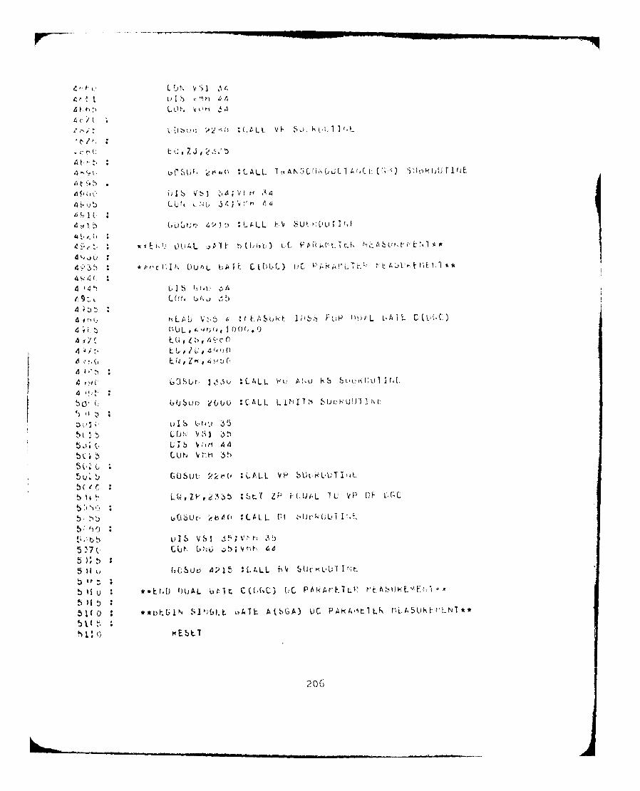
K vB ,. *' :[,,LL vi SUi k 1.l.,] v ti
4 ,-/,u :
4~4
4 Li 15 ~ A~
db, h :
uSt L H N
4 u LUI A -:' V flv" 4,S6 ; L
LG 0
' ]b GLUL: 22,t: ; LAL.L V. SUt.r:LuTIdt
L ;
4 oi : M %:L4 5) , I -, - 4~U i t" ;b,, , 4 ,4(
5u ,,,( I.N , 2 p *. A- VP ',,Lu (',~it
L ,>v' ,g~ 7 S e :olit L IP 'L Ut' L S I L', P G C Lh
b ' 'S u : *,Lr ,LJ r) . 6 LALL L (,I ' t u JL.' l
ulb VS
5)',f Q **Ijj kP~L'L L.T G)CCP5~ N!i~~U~L~*
5 17USUV 42 1,t A LL Li t
5E;b
5X 0 1! **H- IW L S l I , At~ c C J ) A' .L L.
50, 0 * IN SI G UC PAk 'TMi 0KL 1
206

5tl, V V i t
5...'.' : *. LT br fr. ,' +, b£ tfI ".t S ArN.U ,'. i ,. i ,;.Y."I..'Tct
2: 1' LL ,.,c. L.: ,..' ; ' . ; bi; vsl
51AtL :
' : h l,.. J , U',.. .(V & ,.ST',, "
511) ALLV~A j . A S N
.
ell L3U u L'ti kL L' NV I i,
U eL, , 1' ,
5 I ,:
Lhl{ T : P S POO I. "N(, 1) XL y "I T I
, 01 A. C, , U .. . i' : I*
Pt A
~4 3
-(I,. 1"E 7 b AuV r,, 7 l L ),l j L ~ J L,11Ll j
,t v
b A' P,' A
b+.:?r L , L 'N T,. i ,+,,' ", . mL '-iI: (L1A.L (V ', IkM .
*E'
207

)>I -c.AW vs- . 4I , t 'b t.{kkL TA I
:C L.
'.'.'7t" PAU!I L I *,."L ','T
C. A V
L) t , 1 A I . L 0 A (. 6 A L! CUL'T, ' -, I !i,, Ir, h L I ]I T L b
S.I. , S " . Vt"
HAS H.: FI!, I. L 4, C L
Si. : : 7., Ti /1 T W;T, I.,; (4
*~~~~W L I kh 'i .1
,* ,. DL'f 6"
L I S( t I O,I'.I . , /
3,1,
Sr L T . v1 U t vr*l nL IvUEiA fA.
I .' G " ILL00
..~ ~ i- I . ,
",.'., , ~ ~ ~ ~ L P, .Lfi I t I X.] l.fS 'l ,i, . 1P <i T. t, J l l'L V
7 . tL it l~ . A% ;P L ' I' ,
'T'~ ~ t u;
L.,' L'' L.'l t,
.L: I(. i~ ~~~~~~~~ ~~~~~~~ UL .I ,L: ,,
A'. , l , ,t- VIIA _V ) V~b Fr'T
, c.~~ ~ ~~~~~~~~~~ L L), Fir k ,C Ll Y l [,. t
F i'.L F f:iU I TIL AD f.*
.L -I .5O .
: r. , ,o

, V,. ) -. *fr. -e, A~: it" 1'C, v . ,b JLL)
L . U /
,/,j~ S11, V~ Y ,",.. I .4 4 mr LL L S t IJ
r',' ), " ~ LS
1. " ,s) ar ,Tt Y tf C I'L2' L L S: Ir-' T L( VP ,a I (Y)
I Ij
U L 1C t) J A) ' i UII L T S It;
"vi ,.1, ,L W~..L t ,Lr "
4. ) 0 tI 4 1 T hi l C I Y
. t N ,.T F bmA
20-9 :
', - ,t b tNL;] I-;,L SIr~~-( iT F-1r,S ,. *
,", u .,209

APPENDIX J
FOUR-BIT ACCUMULATOR TEST RSL1
AND CONCLUSIONS
210
AP'IK}V IX J
FOU -B T A T T A, ' T, I I T ,
The objective of the t to .tp n the
procedures, obtain results, an hs-.-; 'on the aUtor:.--
mated testing of the 4l-b1)! t A '71. accumu c. ir
67 and CS. The accumulator a . e:J gncd n1i"] deveslC d L,-y the
Microprocessor Desi7,n course (EEC .9/C.9C<) students at ! in
the Spring and Summer Quarters of 197F. The advisor and teacher
for this effort was Major J M. Bory. The accuuulator. ;:s
developed and finally fabricated u , the I n T _
circuit fabrication facilities. The Singer tester was us:,ed to
perform the testing of the accumulator.
Design Operation of the !-'Dit Accumulator
Referring to Figure C7, the accumulator acceots 'I data input
(DB0-DB3) with a total of 2 or 16 co..binations as shown in Table
XIII. The accomulator is to perform the following data oper o:
parallel load, shift left, shift right, rotate, and nothing.
Control signals CACCZ, CACCI, and CACC2 control the operaticns
which are listed in Table XIV.
211
CrF
-1 -9
LC-)
LnL
Cl)
C4-

i-
"'. Acum la o Ch
- 213
t lt -1; _. - I .L_-_ _
I .b - . . . -. . .. .
i ,. ii t- .... .. '.. . . . .
"." ' ..... ' ....
I t" .< 'i" ':
.i ' i , : ; .. . . .. '* ;I . ... . . .. ... ... ..I i... . . . .". _ .Ii..
• i . ! . I ,< ,I, '"r, \d Pi r: ..
f ' , 7. J"II-" L T•.... . .. .• .. ... I. -K ~
: i ' I - , . ;. , ,,. f
- .I . .. .~ , ' • I... . .
lig , 68 !- , .t Aiu1t, Chin..
213

Table XIII. 4-13it AccimT:u, tcrInpLut D) t:_t.
DB 3 _____ D' 1 _____
0 0 0 0o 0 3 1o 0 1 0o 0 ] 1o 1 0 0o 1 0 1o 1 11 0o 1 1 11 0 0 01 0 0 11 0 1 01 0 1 11 1 0 01 1 0 11 1 1 01 1 1 11
The accumulator was designed and developed using silicon
gate P-MOS transistors. The use of P-MOS devices requires the
use of negative logic inputs. The accumulator also requires
two phase clock signals, Cx and y, to transfer the data
(DB0-DB3) to the outputs ACC$-ACC3 according to the aripropriate
set of control signals. The gate requires two biases: Vd
at -7.0V and V at -14.5V. A reset control signal, CFST, isgg
included to reset the accumulator to zero. Since nercative ionic
is used, a logic 1 is set at -7.0 and a logic 0 at, 0.OV or ground
potential. These inputs and their appropriate logic levels are
listed in Table XV. The timing diagram of Figure 6) indicates
the relationship of control to phase clock signals to be usei
to shift data. The designers of the accumulator design the
device to shift data after Cx,}y phase clocks were applied to the
device.
21 1
. . .. " . . . . . . . . .. . . . . . .. . . . . . . . . . . . . . . . . ." .. . . I I II ' - I .. .

A ut omn ', ,d Tos inc l" t i: o'th, - 1, 1,t' c < miuI:it (-r
A means was needed3 to test the- 4-bt accumulator after its
fabrication at AAI,/AMd,. The i n,.ger tester was a logical
choice to test the accumulator ait the wafer level. In order
to test the device, a probe card as requirel to be devei ed
to interface the device with the Sinner tester. The prol¢, card
was inserted into the TAC probe unit just as in the testin-
of the MESFET. Table XVI lists the functions of the bon,3.-
pads and the assignod probe card, pin numbers.
Automated Testinm Procedures. Now that the functions cf the
various signals have been noted, it is now time to state the
testing procedures used to determine the performance of the
4-bit accumulator. The following is a simple algorithm adopted
for one particular testing, procedure for the Singer tester:
1. Reset the Singer tester.
2. Set up the appropriate power supplies.
3. Input desired data.
4. Apply desired control signals to either parallel load,
shift left, shift right, or rotate the deisred data.
5. Apply yxy
6. Stop.
The above algorithm was implemented into a program to be used
on the Singer Tester.
Automated Testing Results and Conclusions. The objective
of the testing of the 4-bit accumulator was to determine if it
was capable of performing the data operations as indicated in
Table XIV. The little known fact in the testing of the 4-bit
accumulator was that of the clock rates that were required
215

to transfer data to the outputs ACCO-ACC,/. This wa- not
available in the provided documentation nor from a consultat ion
with one of the designers of the accumulator. From Chapter VT,
it was noted that the highest frequency available on the 2ing-er
was about 62.5 Hz. Consultation with the advisor in.*ica t.'d
that the clock rates required for the accumulator were sori.ahat
higher. As a result, no valid data was obtained fr:;i th,
accumulator testing. The main problem experimented in usin
the Singer was that the clock rates and therefore th(u, period
and pulse widths of the control signals could not be controlled.
Given the fact that these characteristics were unknow;n, made
it even more dif'icult to provide the proper signal characteristics
required by the Sin-er. The source code was not capable of
p-roviding the proper signal characteristics required by the
accumulator whatever they were. The source code provides mainly
for static testing only and is limited to the testing of DC
parameters. A further study of this area is presented in
Chapter VI.
In conclusion, the Singer tester is not capable of providing
variable clock rates to the degree of flexibility required by
some circuits. From the testing it was discovered that the source
code was also not capable of providing the clock pulses x, y
as in Figure 69 due to the fact mentioned above. x would
simply overlap . The automated testing of the 4-bit
accumulator served as a basic exercise to understand the
Elucidate testing language and testing techniques, the
Singer tester itself and its capabilities. This ex!,erience aided
in the development of the automated testing programs to test the
GaAs MESFETs of Figure 19.
216
I1

Table XTV. 11l'Pit Ac~umubItorControl21ni.
CACCO CACCI CCI FL:*.cTJ'I C,
0 0 PARALLEL11 LOAD1
1 0 P OHIT CH
10 T0 1 ROA%
Table XV. 4--Pilt AccumulatorVoltar-e Inputs.
VOLTAG7 FITS HIGE LOW
CACCO.-CACC2 -7.0 01.0
D 9--D T3 -7.0 0.0
CRST(RESE7) -7.0 0.0
V DO -7.0 0 r)
V GG -7.0 0.0
x-7. 0 0 .0C
2f-7.0 0.0
CARPO -7.0
217

Table XVI. 4-P,1.t Ac~~c rbCard Interface Connections.
BOIDING PAD FUNICTION PIN' 1:UMD11LR
ACCi 1
AC C2 2
DB 2 3
CARRT4
M3 1
RE SET 6
DBO 7
CACC2
CARRY79
CACCO 11
DB 3 10
CACCl 1
ACC3 13
ACCI 12
V GG 1~5
x 16
ON D 17
v DD 18
y 19
V GG 20
218]

-- -U'__
)toCO
0
to
CO
CL~
- -- -.----- -- --- 0
C:0C)
C)
toC:0
c-s
0)
C:
0
GO
CO
CO
~J) CO
*~-I C)
*~-~ r-~
no
0-'\DPJ
C) C~) GD El-'C) CD C)
C) GD
rt.
219

Autoa', Te:tivn Proce.ures. New that the fiinctions of
the various si.,-nals have been noted, it is now time to state
the testin,, procedures used to deter:iine the nerformance of the
4-bit accuaulator. The following is a simple al-orithm
adopted for one part-Icular testin- procedure for the S]ncer
tester:
1. Reset the Piner tester.
2. Set uu the appropriate power supnlies.
3. Input desired data.
4. Apply desired control si-nals to either parallel
load, shift left, shift right, or rotate the desired data.
5. Apply x'¢y,
6. Stop.
The above algorithm was implemented into a prog ram to be used
on the Singer Tester.
Auto~mated Testin, Re. . t. and Concli--ios. The objective
of the testing of the 4-bit accumulator was to determine if
it was capable of performin- the data operations as indicated
in Table XIV. The little known fact in the testing of the
4-bit ace,mulator was that of the clock rates that were
required to transfer data to the outputs ACCO-ACC3. This
was not available in the providedI documentation nor from a
consultation with one of the dusI gners of the accumulator.
From Chapter VI, it was noted that the highest frequency
available on the Singer was about 62.5 Hz. Consultation
with the advisor indicated that the clock rates required for
the accumulator wore -,omewhat hirghe.r. As a result, no v.lid
data was, obt-a i ned.. fro, the accu.iul ator testinr. Th, main
roble , X C, 2rlec, in uslng, the , tnj[lr Was t hat the co j(C-
220

rates and therefore the period and pulse widths of the control
signals could not be controlled. Given the fact that these
characteristics were unknown, made it even more difficult to
provide the proper signal characteristics required by the
Singer. The source code was not capable of providing the
proper signal characteristics required by the accumulator
whatever they were. The source code provides mainly for
static testing only and is limited to the testing of DC
parameters. A further study of this area is presented in Chapter V1.
In conclusion, the Singer tester is not capable of providing
variable clock rates to the degree of flexibility required by some
circuits. From the testing it was discovered that the source
code was also not capable of providing the clock pulses x3 y
as in Figure 69 due to the fact mentioned above. x would simply
overlap . The automated testing of the 4-bit accumulator
served as a basic exercise to understand the Elucidate testing
language and testing techniques, the Singer tester itself and its
capabilities. This experience aided in the development of the
automated testing programs to test the GaAs MESFETs of Figure 19.
221

APPENDIX K
SINGLE GATE DC PARAMETER MODEL DATA
222

TABLE XVII DC Pa.ameter Data For Source Follower Characteristic
Curves, Fi-ure 14.
IDSs~fA) = 11.6
v (v) = 08.0
gm(mmho) = 2.2
Rd ( o 1h m ) = 3.0
I (mA)
V (V) V (v) R (Ohm) R_(Ohm) CAfLC . .EAS . G ipS_ __ _ GS 0_ _ _ _ _ ___ _ _ _ _ _ _ _ _
0.0 0.0 184 2500 0.0 0.00.5 2.71 3.20.0 5.84 6.0 LITE A T31.5 8.1 8.42.0 10.8 10.3
2.5 0.0 184 250n 11.7 11.53.0 11.96 11.93.5 12.1 12.0 SAT4.0 12.33 12.34.5 12.52 1.2.55.0 12.7 12.6
0.0 -1.0 229 2500 0 00.5 2.18 2.81.0 4.80 5.2 L E,,1.5 6.55 7.22.0 8.73 8.8
2.5 -1.0 229 2500 9.01I 9.43.0 9.22 9.6:3.5 9.40 9.8 SAT4.0 9.69 10.04.5 9.77 10.25.0 9.95 10.4
0.0 -2.0 294 1785 0.0 0.00.5 1.7 2.41.0 4.0 4.4 L'NEAR1.5 5.1 5.8
2.0 -2.0 294 1785 6.55 6.52.5 6.79 6.93.0 7.03 7.23.5 7.27 7.5 SAT4.0 7.51 7.64.5 7.75 8.05.0 7.99 8.2
223

]Dm )
VDS (V) V (V) o (Chm) H (Ohm) CALC. MEIAS . P OU ll
0.0 -3.0 416 2500 0.0 0.00.5 1.2 1.8 SAT1 .0 2.7 3.0
1.5 -3.0 416 2500 4.1 3.82.0 1.5 4.42.5 4.73 4.6 SAT3.0 4.90 4.83.5 5.0 5.1
4.0 5.25 5.2 SAT4.5 5.4 5.65.0 5.59 5.7
0.0 -4.0 675 2500 0.0 0.00.5 0.8 0.81.3 1.6 1.61.5 2.3 2.0
2.0 2.7 2.2.5 2.9 2.63.0 3.1 2.83.5 3.2 3.04.0 3.10 3.24.5 3.65 3.45.0 3.80 3.6
0.0 -5.0 1250 2500 0.0 0.00.5 0.4 0. 1! LINEAR1.0 0.8 0.8I : 1.2 1.12.0 1.5 1.2
2.5 -5.0 1250 2500 1.75 1.4
3.0 1.88 1.593.5 2.00 1.7 SAT4.0 2.15 1.94.5 2.28 2.05.0 2.42 2.2
0.0 -6.0 2500 2500 0.0 0.00.5 0.2 0.2 LINEAR1.0 0.4 0.14
2211

V~ ( ) V(V) V)-T \O~: . r', : ' ) :ALC. ( ;.; . .. _._____; ___-r
Vv (V) v>2. -
1.5 -6.0 2500 0.66 0.702.0 0.76 0 .o2.5 0. 86 0.823.0 0.96 0.98 2AT3.5 1.05 1.5.0 1.26 1.205.0 1.36 1 .40
0.0 -7.0 5%00 2500 0.0 0.00.5 0.1 0.2 I--.AR1.0 0.2 0.22
1.5 0.26 0.302.0 0.33 0.402.5 0.39 0.423.0 0.46 0.463.5 0.52 0.70 SAT40 o0.59 0.80u.5 0.66 0.815.0 0.73 0. 82
0.0 -8.0 0000 2500 0.0 0. 00.5 0.05 0.1 LT E UA1.0 0.1 0.1-5
1.5 -8.0 10000 2500 0.12 0.22.0 0.16 0.212.5 0.24 0.393.0 0.26 0.40 sA'3.5 0.28 o.414.0 0.319 0.424.5 0.36 0.4.!5.0 i 0.40 0.46
225

APPENDTX L
ALTERNATE VMETIO1- T C .. E C UR R'
MEASURING INACCURACY Cl THE SIN:GER TE'STER
226
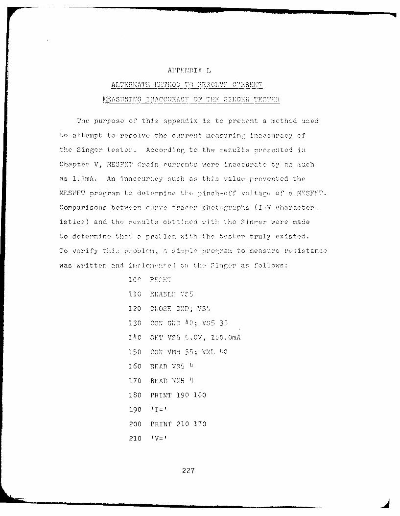
APPENIP1lX L,
ALTEBE "ATE 71TE -) ?31Y M E
MEASURTNG NM A(URCY P TillE i11:GF TEI.)?
The purpose oif thi s appendix is to ore-,ent a m,,ethod used
to attempt to resolve the current meacuriri>' inaccuracy of
the Singer tester,. According to the results prrsented1 in
Chapter V, MES'1' d"rain rurrents were inaccurate ty a,,? much
as 1. ImA. An inaccuraey such as this value- prevented the
MESPET program to determ-ine the pinch-cff voltare of a M-SFET.
Comparisons betweecn curve tra(cer phtrrps(I-V character-
istics ) and the eslt obta-IreA .. itlh tho Sinrecr ,,eTre made
to determi ne tht roblle% wi-:th thr tester, truly e'xisted.
lo Verify tIs -ro.-All aSirn!e pro-ram to measure resistance
was written anclU Ie*n on cli the ge as follows:
-10() BESE
120 CLOCSE-, GND; %VSS-
130O CON GIND 110 V IS 3'
1110 SET VS5 S. CV, ltU0.0mA
150 CON VMH 3 5; VYL h0
160 READ VS 4$
170 READ VMH It
180 PRINT 190 160
190 'I=,
200 PRINT 210 170
210 'V='
227

220 P AUSE R0 " H, OF, . 1......
230 INSTRUCTS TQ OA, CONTINUE.
240 PRINT 250
250 '
260 GOTO 160: MEASURE IEXT RE, SIATACE VALU:.
270 END
A decadc resistance box was connected across pins 35
and 40 of the performan e boar(. The resistance was increa- ed
by 1,000 ohms when the program halted each time at line 220
above. The maximum resistance .set on the decade box was
50,000 ohms. The voltage was set at 5.OV with current measured
at each value of resistance. The actual current was calculated
using ohms at each value of resistance. Experimental currents,
were measured on the Si nger for each value of res]st ance.
The results obtained and the error factors are shown in
TableXVTliIfor values of resistance between 5,000 and 50,000
ohms at 5,000 ohm increments. The error factors were calculated
by dividing calculated values of current by the -m)easured valuer.
Table XVIIICurrent Mearurin, Accurac, of the Singer
CALCULATI.D S, ,, II ER!O
RESISTANCE(Ohms) CURRENT (mA) CURR ! TV.. FACToR
5000 1.00 1.86 0.5310000 0. 50 1.3; 0.3715000 0.33 1.35 0.3720000 0.25 1.12 0.2225000 0.20 1.08 0.1830000 0.17 0.02 0.1735000 0.14 1.01 01.340000 0.12 0.99 0.1245000 0.11 0.98 0.115000 0.10 0.9(6 0.10
228
.. .. II III II 111 171 - d

Error factors fcr currents for resistances between 1,000
and 50,000 ohms were obtained but not sho,..,n in the table. A
mean error factor value was then obtained for several values of
current throughout the resistance range. The M,.EFET program was
then set up to multiply a drain current by the appropriate error
factor when thc measured current was within the current range
for the specified error factor.
Using the above method to cbtain the proper drain currents
did not prove fruitful. The objective was to develop a simple
method to resolve the current measuring inaccuracy of the
Singer as discussed in Chapter V. Solving this problem would
hopefully provide the capability to obtain pinch-off using the
MESFET program since current measuring accuracy is important.
Another but similar method was then attempted to resolve
the current accuracy problem. Without going, into detail,
curve tracer I-Vcharacteristics (Figure 70) were obtained fOcr!
a SOURCE FOLLOWER MESFET. The same MESFET was then tested on
the Singer to determine experimental values of drain cur'rent
(Table XX). Error factors were determined for values of curni-nt
as shown in Table XTX.
Table XTX. Error Factors Used to Resolve Current Measurn,
Tnaccuracy of the Sin7cr.
CURRENT RANGE (mA) ERROR FA,'T1()OO
4.0 to 8.5 0.843.0 to 3.9 0.7112.25 to 2.9 0.641.70 to 2.24 0.541.45 to 1.69 0.451.27 to 1.44 0.381.20 to 1.26 0.30 Cent.
229

Table XIX Continued.
CURRENT RANGE (mA) ERROR FACT'OR
1.15 to 1.19 0.251.11 to 1.12 0.221.07 to 1.10 0.121.o to 1.06 0.100.05 to 1.00 0.050.00 to .014 0.01
230
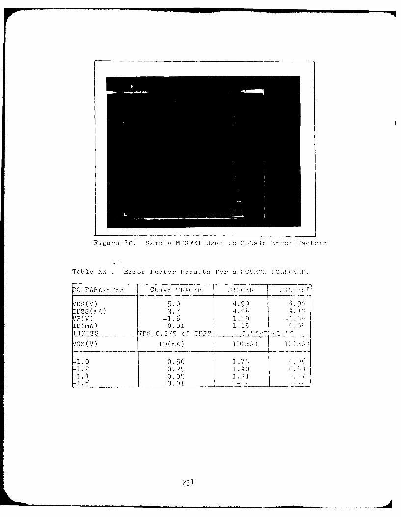
Figure 70. Sample MESFET Used to Obtain Error Factor2.
Table XX Error Factor Results for a SOURCE FOLLI".<.
DC PARAMEPER CURVE TRACER TUGER 7' , '
VDS(V) 5.0 4.99IDSS(mA) 3.7 4.04VP(V) -a.6 1. 59 -1ID(mA) 0.01 1.15LIMTTS V1PP 0.27% of TDSS 0_._I,-,_____ _ ._ F
VGS(V) ID(mA) TI)(mA)
-1.0 0.56 1 •7.-1.2 0.25 .40-r1.4 0.051.6 0.01.
231

VITA
Thomas Lindsay Harper was born on 19 April,1955 in
Jackson, Tennessee. He graduated from Gulfport East High
School, Gulfport, Mississippi, in 1973. He later graduated
from the Mississippi Gulf Coast Junior College, Jefferson Davis
Campus, Gulfport, in 1976, receiving his Associate of Science
Degree. He then attended Mississippi State University,
Starkville, Mississippi and received the Bachelor of Science
Degree in Electrical Ergineering and was comissioned from
the Reserve Officers Training Corps program in !lay 1978. Ho
immediately entered the School of Erigineering, Air Force
Institute of Technology in June 19 78. Upon completion of his
courses of study, he joined the Avionics Laboratory, Air Force
Wright Aeronautical Laboratory as the project engineering of
the Global Positioning System Evaluator facility. He is a
member of the Institute of Electrical and Electronic Engineers,
the Aerospace and the American Radio Relay League.
Permanent Address: 94-40th StreetGulfport M"' ) 50
232

UNCLASSIFIEDSECURITY CLASSIFICATION OF THIS PA, E 1'hen Datl F'wterrd)
REPORT DOCUMENTATION PAGE READ INSTRUCTIONS• BEFORE COMPLETINGl FORM
1. REPORT NUMBER 2. GOVT ACCESSION NO. 3. RECIPIENT'S CATALOG NUMBER
AFIT/EE/GE/80- 7 M91 1
4. TITLE (and Subtitle) 5. TYPE OF REPORT & PERIOD COVERED
The Automated DC Parameter Testing of GaAs MS THESISMESFETs Using the Singer AutomaticIntegrated Circuit Test System 6. PERFORMING O4G. REPORT NUMBER
7. AUTHOR(s) S. CONTRACT OR GRANT NUMBER(sj
THOMAS L. HARPER1st Lt USAF
9. PERFORMING ORGANIZATION NAME AND ADDRESS 10. PROGRAM ELEMENT. PROJECT. TASK
AREA & WORK UNIT NUMBERS
Air Force Institute of Technology (AFIT-ENWright-Patterson AFB, Ohio 45433
11. CONTROLLING OFFICE NAME AND ADDRESS 12. REPORT DATE
Sept 198013. NUMBER OF PAGES
23214. MONITORING AGENCY NAME & ADDRESS(if diflerent from Cortrolling Office) IS. SECURITY CLASS. 'ot this report)
AFWAL/AADE UNCLASSIFIEDWright-Patterson AFB OH_____ _______
15a. DECLASSIFICATION DOWNGRADING
SCHEDULE
16. DISTRIBUTION STATEMENT (of this Report)
Approved for public release; distribution unlimited.
17. DISTRIBUTION STATEMENT (of the abstract entered in Block 20, if different from Report)
is. S PPLEMENTARY NOTES
Aro ed for lublic elease; IAW AFR 190-17
FR DERIC C. LYNC,% Major, USAF 16 JUNDirector of Public Affairs
19. KEY WORDS (Continue on reverse sde if necessary and identify by block number)
GaAs MESFETs DC Parameter TestingGaAsMESFETs GaAs MESFET DC Modeling
Automated Testing
20. ABSTRACT (Continue on reverse .ide f necessary end identify by block nrmber)
Procedures, in the form of a computer program, were developed toautomate the manual testing of the DC parameters of GaAs MESFETs,integrated resistors, and Schottky diodes. These devices areelements of a NAND/NOR logic circuit developed by Hewlett-Packard. The Singer Automatic Integrated Circuit Test Systemlocated at the Air Force Wright Aeronautical Laboratories, AvionicsLaboratory, Microelectronics Branch (AFWAL/AADE), Wright-PattersonAFB OH, was used to develop these procedures.
DD FOM 1473 EDITION OF NOV 5 IS OBSOLETEUIN CLASSIF I ED
SECURITY CLASSIFICATION GF TN'S PAGE (%ben Datal El ntered)

UNCLASSIFIEDSECURITY CLASSIFICATION OF THIS PAGE(V/nen Data Entered)
The following DC parameters for the above devices were to be
tested using the Singer tester: drain-to-source voltage (VDS),
saturated drain current (IDSS ) at gate-to-source voltage (VGS)
at 0.0 volts, pinch-off voltage (Vp), transconductance (gin),
breakdown voltage (BV) at VGS = 0.0 volts, diode forward and
reverse threshold voltages, and resistance. Procedures have beenwritten to test all of these parameters with actual test resultsobtained for the following MESFET parameters: VDS , IDSS, VGS ,
linear on-resistance and saturation resistance, VP and gin"
Unfortunately, due to system measurement accuracies, these resultsdo not compare favorably when compared with curve tracer I-Vcurves of the MESFETs. This report will attempt to demonstrate thfeasibility of the Singer to test these parameters given thestatus of the system.
I
UNCLASSIFIEDSECURITY CLASSIFICATION OF To- PAGr(W7pI M , E a ntered)

DAT
FILMEI
ITI