Embed Size (px)
Citation preview

UNCLASSIFIED
AD NUMBER
AD406875
NEW LIMITATION CHANGE
TOApproved for public release, distributionunlimited
FROMDistribution authorized to U.S. Gov't.agencies only; Administrative/OperationalUse; FEB 1963. Other requests shall bereferred to Army Research and DevelopmentLab., Fort Belvoir, VA 22060.
AUTHORITY
USAERDL Itr, 17 Nov 1965
THIS PAGE IS UNCLASSIFIED
UNCLASSIFIED
AD 406 875L
DEFENSE DOCUMENTATION CENTERFOR
SCIENTIFIC AND TECHNICAL INFORMATION
CAMERON STATION. ALEXANDRIA. VIRGINIA
UNCLASSIFIED
NOIICE: Men government or other drawings, spec-ficaitons or other data are used for any purposeother than in connection with a definitely relatedgovernment procurement operation, the U. S.Government thereby incurs no responsibilityl nor anyobligation whatsoever; and the fact that the Govern-wsnt may have forlaAted,, furnished, or in any waysupplied the said drawings, specifications, or otherdata is not to be regarded by implication or other-vise as in any manner licensing the holder or anyother person or corporation, or conveying anmy rightsor permission to manufacture, use or sell anypatented Invention that may in any way be relatedthereto.
211 LAS-SR-224-12
February 1963
0 /ANGULAR ENERGY DISTRIBUTION OF PHOTOELECTRONS
16 Quarterly Progress Report
16 October 1962 to 16 January 1963(Third Quarter)
8
U Contract No. DA-44-009-ENG-5004
UPrepared for
Warfare Vision BranchU. S. Army Research and Development Laboratories
Ft. Belvoir, Virginia
THE UNIVERSITY OF CHICAGOLABORATORIES FOR APPLIED SCIENCES
CHICAGO 37, ILLINOIS
!IIZ VINSi C:oiTAflhxv HERIU iFLAS-SR-224-12 2MLY U VIffS CO TAIN PPR704=n
February 1963 AM A NOT 0 n AppllV. My
ANGULAR ENERGY DISTRIBUTION OF PHOTOELECTRONS
Quarterly Progress Report16 October 1962 to 16 January 1963
(Third Quarter)
Contract No. DA-44-009-ENG-5004
Prepared for
Warfare Vision BranchU. S. Army Research and Development Laboratories
Ft. Belvoir, Virginia
THE UNIVERSITY OF CHICAGOLABORATORIES FOR APPLIED SCIENCES
CHICAGO 37, ILLINOIS
UO.S. Grfonrt 16o MY Obtain *opt*
*tths ~p~direOtY from AMA. Otbz'quaeit1. AJ2T1A Unoes ShoM14 request tp4l~o~ US L - ort ft ihf
FOREWORD
This report was prepared by the Laboratories for Applied
Sciences of The University of Chicago under United States Army Research
and Development Laboratories Contract No. DA-44-009-ENG-5004,
"Angular Energy Distribution of Photoelectrons," LAS Task 2?
istered for USAERDL by Mr. Edward J. Walker. It covers th.
quarter of the contract from 16 October 1962 to 16 Januar
Laboratories for Applied Sciences personr ?ated
in the work covered in this report include R. Allison, . cn-, F. Gillespie,
E. Pekol, R. Pernic, and M. Remdt.
LABORATORIES FOR APPLIED SCIENCES
Jay BurnsPrincipal Investigator
Approved:
Foster F. RiekeAssociate Director
Ir
LAB-SR-224-t2 ii
S!
ABSTRACT
Initial test results on the experimental tube and associated
apparatus are described together with certain changes suggested by the
test results. Problems connected with making S-9 photocathodes by the
atomic beam cesiation method have delayed angular distribution measure-
ments. A tube is described which was built for experiments to correlate
photoelectric properties with impurity concentrations in photocathodes as
determined by Hall effect measurements. Certain theoretical aspects of
the angular energy distribution are discussed.
LAS-SR-224-i2 Mii
I
1. EXPERIMENTAL
Experimental work during the reporting period centered on testing
the comp!lete experimental apparatus and especially the tube in which measure-
ments are made. Several changes in tube components were made as a result
of the tests. These will be described below.
A second experimental tube was built to measure the excess carrier
concentration in photocathodes by the Hall e- "ect and to measure yield, spectral
sensitivity, and energy distribution of photoelectrons (integrated over all
emission angles) in the same photosurfaces. The objective here is to study
the relation of these photoelectric characteristics to the excess carrier concen-
tration with emphasis upon the relative contributions of the surface and volume
photoeffects in Cs 3Sb. It is important to have some information about the
relative importance of surface and volume effects before the energy angular
distribution can be treated theoretically. This point will be discussed more
fully in the theory section.
1. 1 Vacuum Processing and Components
Helium leak testing revealed small leaks in a large inconel bellows
that transmits motion into the angular distribution tube to rotate the photocathode
(see Ist Quarterly Report, LAS-SR-224-4). These leaks either developed in a
heliarc weld that was inaccessible for repairs once the tube was assembled, or
they were due to a porous section of the bellows that developed during vacuum
firing prior to assembly. In any case there was no way in which the leaks could
be sealed up directly, short of rebuilding A major part of the rotation trans-
mitting mechanism. To avoid this, an attempt was made to seal the leaks
with an epoxy coating. A water-thin coating of Fuller's Resiweld(l) 7?Z1 thinned
2:1 with SOV-3 thinner was applied to the atmospheric side of the bellows with
1. H. B. Fuller Company, St. Paul, Minnesota
LAS-SR-224-12
a brush while the tube was evacuated and the coating was allowed to cure over-
night. This treatment was completely successful in sealing the leaks permanently.
No leak larger than 10"13 liter-atmosphere/sec (the sensitivity limit of our
Veeco MS-7 leak detector) remained, and the tube stayed vacuum tight after
prolonged baking at 250 C. This temperature was regarded as the safe upper
limit for baking out the epoxy coating; unfortunately such a temperature does
not suffice for outgassing the tube very rapidly, and about two weeks of pumping
with daily bakes for sev-ral hours at 250 0 C were needed to evacuate the tube
to the 10"9 torr regit -i. The lowest pressure attained was 2 x 10"9 torr with
the valve to the diffusion pump closed and a 1 liter/sec VacIon appendage pump
in operation on the tube. The only getter used was a titanium-wrapped tungsten
filament from which a little Ti was evaporated in a small attached ionization
gauge. Molybdenum getters in the main tube (see 1st Quarterly Report) were
outgassed but no Mo was evaporated in order to avoid any premature loss of
tube wall light transmission.
The first quarterly report described an all glass, bakeable, ultra
vacuum valve that was developed for this project. The valve uses indium as
a sealing material and operation of the valve entails melting the indium and
inserting a large diameter glass tube into it. The seal depends on molten
indium wetting the glass and maintaining intimate contact when it solidifies.
The conductance of this valve is high, and it has proven generally satisfactory
through a number of tests. Occasionally, the surface of the glass tube that
must be wet by indium to make a seal gets contaminated during bakeout, and
a leaky seal results. While such a failure is infrequent, it was a cause for
some concern. Fortunately, during the quarter a bakeabLe. indium valve(2 )
having a more positive acting seal appeared on the market. This valve operates
by forcing a modified knife-edge into an indium washer, but it differs from other
2. Kane Engineering Company, Palo Alto, California
LAS-SR-224-12 2
metal-to-metal valves in that very little torque is needed to close it. Conse-
quently, it is relatively light and need not be mounted in a heavy, rigid fashion.
Moreover, it can undergo many closures before the knife edge goes clear through
the indium washer, and should this happen, it is a simple matter to remelt the
indium under vacuum to re-form the washer. Since the seal does not depend
upon indium wetting any surface, it is not affected by anything driven out of
the tube during bakeout. Finally, the configuration of the valve makes a
simpler, more compact mounting possible giving needed additional clearance
for the angular distribution apparatus in the bakeout furnace and in the Helmholtz
coils. The new valve was installed at the close of the reporting period and we
have not yet had time to test it thoroughly.
Experiments to measure the rate of deposition of molybdenum as
a getter material from . 015" dia. filaments revealed that thermal conduction
to nickel support wires was sufficient to cause some evaporation of nickel.
Since it is intended that Mo deposition in the angular distribution tube shall
also serve to produce a uniform standard work function everywhere in the tube,
vaporization of nickel with the Mo should be avoided. Substitution of . 010" dia.
molybdenum operated at 22000K (5 amperes) satisfactorily removed this difficulty.
It was found that the transmission of a clean glass surface 4 cm. from such a
filament (a 3-1/2" length of wire wound into a 1/8" dia. loose helix) was reduced
by 10% in 24 minutes by Mo deposition. Rough estimates of the optical constants
of Mo films (reliable values do not seem to have been published) indicate that at0
least 20 A thickness and quite likely more is required to reduce light transmission
by 10%.
The necessity of our knowing fairly accurately the time required to
deposit a monolayer to avoid premature darkening of the tube wall prompts us
to continue to investigate the rate of deposition of Mo films on glass. A colori-
metric chemical analytical method has been chosen which should be sensitive
enough to measure the 90% transmission films we are dealing with. The method
LAS-SR-224-12 3
was originally devised for biochemical assay work and required modification.
This has been done, and an initial determination has been made on a 90%
transmission film deposited on a 1" dia. Pyrex window. This determination,
though only to be regarded as tentative yet, indicates that a much thicker0
layer (order of 150 A) was deposited than the estimated optical constants suggest.
Final results of this work will appear in the next quarterly report. A by-
product of the work will be a good set of optical constants for thin Mo films
on glass.
i. 2 Photocathodes
An 4.aitial attempt to make an S-9 photocathode in the Hall effect
tube by the atomic beam cesiation method(3) failed because of insufficient
cesium in the reservoir of the beam oven. Only a very low photosensitivity
developed in this cathode even after prolonged cesiation, and the first color
change indicating formation of the compound CsSb only appeared near the edge
of the Sb deposit where the antimony layer thinned out. A second attempt to
make a cathode in this tube also failed because a defining aperture in the
antimony beam became misaligned with the result that the cesium beam did
not land on the Sb deposit.
Initially S-9 and S-1i photocathodes are being deposited over a
stannous chloride conductive coating on a Pyrex glass substrate. The use of
Pyrex here is a matter of convenience until plates of Corning 7052 glass of
suitable thickness can be obtained. Then cathodes will be made on this glass,
again with the conductive coating since use of such coatings is fairly common
in image tubes. It is not likely that any differences will be found that can be
attributed to the substrate glass type since it is believed that the stannous
chloride coating serves as a fairly effective buffer between glass and photosensitive
layer; in any case the differences in composition between 7740(Pyrex) and 7052
3. 1k. E. Simon, A. H. Sommer, B. H. Vine, "Improved Uniformity of Photo-
Cathode Sensitivity" ASD report #ASD-TDR-62-619 (Nov. '62)LAS-SR-224-i2 4
are not likely to result in appreciable differences in impurity concentration in
the photocathodes. The situation is different with soft glass substrates such as
Corning 0080 lime-soda glass. It is difficult to produce a good stannous chloride
conductive coating on lime-soda glasses by the vapor method we ordinarily
employ. When uqed as photocathode substrates without such a conductive coating,
soft glasses release appreciable quantities of sodium and potassium from the
glass into the newly forming photocathode under the action of hot cesium vapor,
and these alkali metals enchance the sensitivity, especially in the red. When
the cathode is cesiated by the beam method, it is probable that there is much
less release of Na andK, especially if the substrate is not heated very much,
and under these conditions one should get a cathode that more closely resembles
those produced on Pyrex or 7052 glass. So far this latter statei ent is a
conjecture since we do not know of any comparison of cathodes prepared on
different substrates by the atomic beam method, but we plan to look into this
matter as time permits during the coming quarter using the Hall effect tube
to prepare and measure the photocathodes.
i. 3 Hall Effect Tube
Several years ago Sakata(4 ) made a rather extensive investigation
of the signs and densities of free carriers responsible for conduction in cesium
antimony photocathodes using Hall effect, resistivity vs. temperature, and
thermoelectric power to determine that in unoxidized Csa b surfaces (S-4 and
S-9 photocathodes) the carriers are holes (p-type conduction) and the densitiesrag rmaot115 -3 017 -3
range from about 10 cm to about 10 cm and .)ccasionally somewhat
higher. It is most dnfortunate that Sakata neglected to make any photoelectric
measurements on his surfaces from which some correlation between carrier
4. Sakata, T., J. Phys. Soc. Japan 8, 125, 272 (1953) and 9, 1030 (1954).
LAS-SR-224-12 5
concentration and photoemissive properties might have been made. The
need for such a corn elation becomes acutely apparent when one sets about
developing a theory for the energy angular distribution from Cw3 Sb photosurfaces.
We are therefore undertaking to remedy Sakata's omission by studying Hall
effect, spectral sensitivity, and integrated energy distribution of various
photosurface. in a tube of relatively simple configuration and of a size that
will fit into a magnet that we have which produces a conveniently large field
(1000 gauss) in a suitably large region (- 31t x 3" x 3").
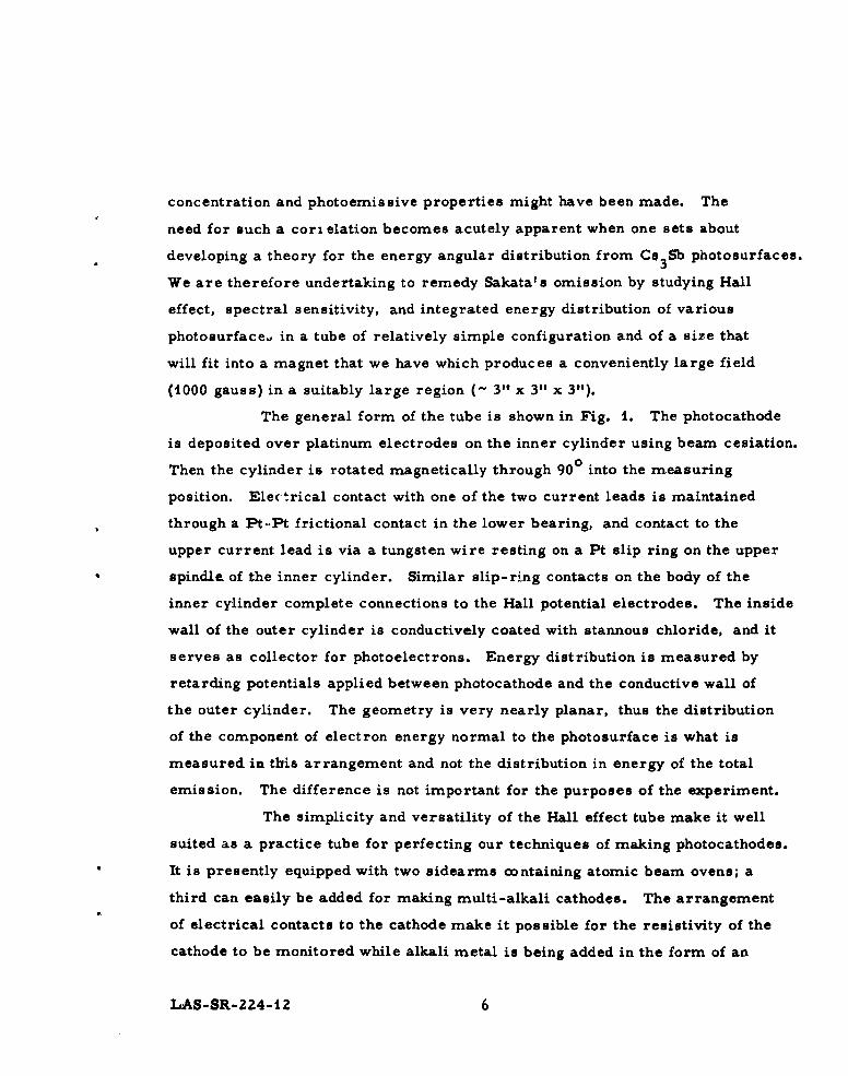
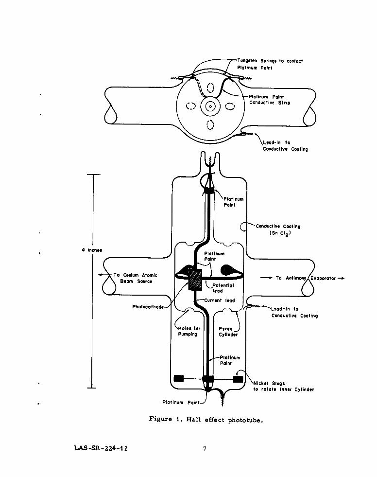
The general form of the tube is shown in Fig. i. The photocathode
is deposited over platinum electrodes on the inner cylinder using beam cesiation.
Then the cylinder is rotated magnetically through 900 into the measuring
position. Electrical contact with one of the two current leads is maintained
through a Pt-Pt frictional contact in the lower bearing, and contact to the
upper current lead is via a tungsten wire resting on a Pt slip ring on the upper
spindle of the inner cylinder. Similar slip-ring contacts on the body of the
inner cylinder complete connections to the Hall potential electrodes. The inside
wall of the outer cylinder is conductively coated with stannous chloride, and it
serves as collector for photoelectrons. Energy distribution is measured by
retarding potentials applied between photocathode and the conductive wall of
the outer cylinder. The geometry is very nearly planar, thus the distribution
of the component of electron energy normal to the photosurface is what is
measured in this arrangement and not the distribution in energy of the total
emission. The difference is not important for the purposes of the experiment.
The simplicity and versatility of the Hall effect tube make it well
suited as a practice tube for perfecting our techniques of making photocathodes.
It is presently equipped with two sidearms containing atomic beam ovens; a
third can easily be added for making multi-alkali cathodes. The arrangement
of electrical contacts to the cathode make it possible for the resistivity of the
cathode to be monitored while alkali metal is being added in the form of an
LAS-SR-224-12 6
Tungsten Springs to contact
Conductive Cotring
Conductive Coating
(Sn C12 )
4 inches Paiu
To Cesium Atomic -pTo 'Antimony Evaporator -- pBem Surce
Photocathode--'1 ý La l t
(?7,,Conductive Coating
Hole s for PyrexI
to rotate Inner Cylinder
Platinum Point)
Figure 1. Hall effect phototube.
LAS-SR-224-~12 7
atomic beam, and this is expected to be a help in processing S-20 surfaces.
The cylinder within a cylinder configuration is also helpful in keeping each
alkali metal confined to its own sidearm during multialkali processing.
The Hall effect tube is normally pumped and baked out on a well
baffled oil diffusion pump, gettered and sealed off, and subsequently pumped
by an ionization gauge containing a titanium evaporator as described earlier.
There has been no difficulty getting and maintaining a vacuum of 10" torr
with this arrangement even while cesiation is being carried on. It is of course
necessary to degas the Sb and its evaporator thoroughly before seal-off and
to degas the Cs pellets and finally to fire them before seal-off to get a good
vacuum in the tube. The initial attempts at preparing S-9 cathodes mentioned
earlier were all carried out in the Hall tube.
2, THEORETICAL
2. 1 Introduction
During the reporting period we began a theoretical study of several
aspects of the angular energy distribution of photoelectrons from Cs 3Sb. The
work is still fragmentary as yet, but certain interesting features have already
emerged, and we will give a brief account of these.
It is customary and convenient to divide the overall process of photo-
emission into four independent mechanisms:
Step 1. Penetration of the light wave into the surface layer of the
photocathode. This in itself is a formidable problem to handle correctly. It
is ordinarily treated by assuming the optical constants of the surface layer are
independent of distance from the surface (which they are not) and applying class-
ical electromagnetic theory to wave propagation in a homogeneous slab of
material with constant refractive index and conductivity. The validity of this
approximation does not seem to have been carefully examined, but it may be
considerably in error. We shall discuss this question at length in a future
LAS-SR-224-12 8
report in terms of a definite model of the surface conductivity of a semiconductor
like Cs 3Sb.
Step 2. Optical excitation of electrons from the valence band of the
semiconductor into the conduction band. This is ordinarily considered the least
complex and best understood of the four processes we are discussing. How-
ever, it has much in commor. with step (I) above. For example, the optical
absorption depends on conductivity which in turn depends on the optical excitation
of valence electrons to the conduction band in semiconductors and insulators.
Thus our steps (i) and (2) are not as independent as might appear at first.
Furthermore, relatively few treatments of the primary photoabsorption process
in the literature have taken properly into account the detailed properties of the
solid particularly in regard to the effect of the lattice on the directions in which
the excited electrons move initially away from the excitation site. More will
be said about this point later.
Step 3. Motion of the excited electrons toward the surface. This is
undoubtedly the least understood of our four processes involving as it does the
extremely complex many-body interaction of the relatively energetic conduction
electron with the other electrons and with the phonons of the solid. Behavior
of conduction electrons in semiconductors near thp bottom of the conduction band
is fairly well understood, although a number of features of collective interactions
of even these electrons is still relatively obscure particularly in polarizable
solids. We are referring to the motion of slow polarons. But the behavior of
fast polarons, the quasi-particles that we have principally to deal with in studying
motion of internal photoelectrons with enough energy to escape, is an area of
theoretical solid state physics that is virtually untouched. It is only within the
past few years that attempts to deal with the polaron ground state have borne
fruit. (5) Lacking any better guide we are forced to back to a fairly elementary
5. H, Frahlich, Advances in Physics 3, 325 (1954).0. R. Allcock, Adv. in Physics 5, 412 (1956).
LAS-SR-224-12 9
approximate treatment of the fast polaron by Fr~hlich and Mott (6) whose validity
under conditions of interest here is admittedly very shaky.
Step 4. Escape of the photoelectron from the surface. This, too, is
a process that has customarily received an uncritical treatment. The naive
picture of a free electron incident upon a step-potential barrier has been the
basis of past treatments. Occasionally a slightly more realistic shape of
potential barrier has been employed, but little has been attempted beyond this.
In view of the above criticisms why have the existing theories of
photoemission been successful at all? The answer is that the theories are
mainly phenomenological and contain enough adjustable parameters to allow
reasonable agreement with experiment to be secured for many of the grosser
photoelectric phenomena. This agreement does not necessarily mean that the
simplified models of the individual processes involved in photoemission really
describe what is taking place. More likely, the complexities of the actual
mechanisms are somehow averaged out in the gross features of photoemission
so they can be described by a much simpler model. This happens in secondary
emission, for example, and it is common in many branches of physics leading
to the result that one cannot deduce details of the mechanisms from experiments
that measure averages. One must then either devise more sensitive experiments
or attempt to construct more sophisticated models which still give the observed
averaged properties but which also predict additional details that may eventually
be tested.
These remarks are intended as a justification for taking a more
critical view of photoelectric theories. Short of working with single crystal
photoemitters, the present experimental program is designed to provide the
6. H. Fr~hlich and N. F. Mott, Proc. Roy. Soc. A, 171, 496 (1939).
LAS-SR-224-i2 iO
most detailed information possible about photoemission from semiconductors.
It is to be expected that features will be found that are beyond the capabilities
of present simplified theoretical models to account for. In anticipation of this,
the initial objective in our theoretical work is to examine critically the weak
points in present models and to see how these might be improved.
Three topics will be discussed briefly in this report: (1) the role
of the lattice in the photoelectric absorption process that yields an excited
conduction electron and a mobile hole, (2) the influence of the surface in the
latter process, and finally (3) the mobility of an electron with escape velocity
in a polar solid on the basis of the fast polaron theory of Fr5hlich and Mott.
2. 2 Photoelectric Absorption (Volume Effect)
The interaction of an optical photon with a lattice electron in the
valence band of an infinite, regular solid may, as is well known, be treated
by time-dependent perturbation theory which yields the probability
2P12 = "n'jH1 2 P2
per unit time for transitions from initial state i (electron in valence band and
photon present) to state 2 (electron in conduction band, photon absorbed). The
density of final states is here designated by p2 and the matrix element for the
transition is H12 and has the following form in a perfect lattice of infinite extent,
, =e-i2 ( -2 7 A 3V ) e-- d 3r
f= (2 mc- -
This is simply the interaction Hamiltonian between initial and final states of the
electron which have been written in the form of simple Bloch wavefunctions,ik .r
Uk (r) e-- --, forbrevity but which will generally consist of series of Bloch
wavefunctions as required to satisfy the symmetry requirements of the lattice,
the Kubic Harmonics of von der Lage and Bethe 7 ). The interaction term, the
7. F. von der Lage and H. Bethe, Phys. Rev. 71, 612 (1947).
LAS-SR-224-12 1i
0
perturbation, is the A . v term where A is the vector potential of the light
wave. For simple, undamped plane waves
A=A ei(wt k . r)- -- 0
where A contains both amplitude and polarization and k is the wavevector of-O
the light wave. Of course, the proper A to use is much less simple (see comments
at the beginning of this section) but for present purposes the one given will serve.
The d 3 integration variable contains the factor r 2dr andV contains a-i
factor r in spherical coordinates hence H1 2 is proportional to
ei~k_ - kz + k) . r * Ud-Uk rU dr
Z-2 -~i
and will vanish unless k = k + k + n where n is a reciprocal lattice vector such
=2 -1that n a/2r has integer components, a being the lattice spacing. If this quantityholds (conservation of momentum) there remains from the integral only the
factor
E rU drf 2which will be recognized as the dipole matrix element for optical transitions
between states I and 2 in the crystal.
Tha influence of the crystal field appears in two forms in the fcrmulas
above. First, the momentum conservation equation k = k + k + n = k + n
(because k is very small for light waves of the wavelengths that we need consider)
shows that optical excitation can be described by vertical (or nearly vertical)
jumps in the reduced zone representation of energy E vs. k for electrons of
the crystal. This is important because, taken with the density of states function,
it determines just where in momentum space the transitions are most likely to
LAS-SR-224-12 12
occur, and this in turn tells a lot about the angular energy distribution. For
certain common classes of crystals (and Cs 3 Sb appears to be of this type), namely
those having the minimum energy gap between valence and conduction bands
located at k1 = 0, the momentum conservation equation reduces to
which means that every newly photoexcited electron has its initial velocity
directed along a principal direction n in reciprocal space, hence along a
principal direction in the actual lattice, provided n , 0, a condition which always
holds for interband transitions of the kind we are considering here.
A second way in which the lattice influences results is through the dipole
matrix element, JUk r Uk dr. The kinds of terms permitted in the expansions
for Uk (i. e., in the ieubicz Aarmonics) are dictated by the symmetry properties
of the crystal. As a result the matrix element actually consists of a series
of terms, each consisting of an "allowed" type of dipole transition obeying
selection rules quite analogous to those in optical spectra. Thus the selection
rules govern the precise forms of the states that a given valence electron may
reach via an optical transition. Note that both the final energy and momentum
are already fixed by the conservation laws; the selection rules further delimit
the possible transitions. Of these latter the relative strengths are governed by
the magnitudes of the appropriate matrix element terms and by the density-of-
states which require a quantitative knowledge of wavefunctions and band structure
of excited states in the specific solid (here Cs 3Sb) being studied. Solid state
theory cannot provide either with any accuracy at present, but later in the course
of this work we shall attempt some semiquantitative educated guesses about these
things aided by our experimental results.
One interesting point should be mentioned before going on. We have
showed that in Cs 3Sb the newly produced internal photoelectrons initially move
LAS-SR-224-i2 13
along major crystal axes so the angular distribution at the site of absorption
of a primary photon is very sharply peaked. If an appreciable fraction of the
excited electrons can move to the surface of the crystal without undergoing
another strong collision which produces a large deflection it can be shown
that the passage of the electron through the crystal surface into the vacuum
outside may be treated to a first approximation as a refraction by the surface
with predictable effects upon the internal angular distribution. The result is
still a sharply peaked distribution outside the crystal for that part of the internal
distribution that is peaked. In view of the long mean free paths for conduction0
electrons commonly believed to exist in Cs 3Sb (> 200 A ), it would seem likely
that many photoelectrons would indeed succeed in arriving at the surface essen-
tially undeflected since they were initially excited. Therefore, if there is an
appreciable degree of preferred crystallite orientation in a Cs 3 Sb photocathode,
the observed angular distribution should be more or less strongly peaked, the
peaks being superimposed upon a cosine-like background. If no orientationexists and the crystallites are completely randomly oriented, then a simple
cosine distribution would be expected even though a single crystal gives a
highly peaked emission.
Thus far we have been treating the optical excitation of an electron
in an infinite crystal. How does the proximity of a surface affect the results?
That is, how does the excitation process differ in the surface and volume photo-
effects? The answer must lie in the form of the electron wavefunctions that enter
into the interaction matrix H12' While we don't know a great deal about the de-
tailed form of these wavefunctions, symmetry demands that they be strictly
periodic in the surface plane, say the x, y plane,and almost periodic in the
normal z-direction with a term added which depends only on the distance into
the crystal and which in fact decreases as one goes into the crystal, vanishing
at large distances z inside the crystal and leaving only the Unperturbed volume
wavefunctions. If we ignore the small variation in lattice spacing with z as
LAS-SR-224-12 14
one approaches the surface it should be possible to construct a reasonably
good wavefunction as follows: To the volume wavefunction ýk(r), which wasi k . r
explicitly written Uk(r) e - -- earlier, we add a surface function, Sk(z),
which decreases as ea- for z> o (i. e., as one goes into the crystal).
We allow for more general functions S(z) by using a series of the form-a z
- c, e if necessary, but the simpler form will be sufficient for the
present discussion. Finally, the resulting wavefunction, *k = +k(r) + Sk(z),
is further defined to go to zero for all z< o (outside the crystalTand this
may be enforced mathematically by multiplying the 'k written above by a
unit step function which is unity for z> o and zero for z< o. The surface
wavefunction Sk(z) adds three new terms for the interaction matrix H12* 3One of these is a pure surface term of the form Sk (z) VSk (z) d r where
-ihe --2 :-1V stands for the C A_. perturbation term. The remaining new terms in
H12 involve mixed products of surface and volume wavefunctions such as
Q kVSk d 3r. Consider the latter integrals first. They have the general form
r) e-akz -ik . r
2-2
"crystalspace
The exponential term is periodic in x and y but not in z except for large z>>a-i
Thus near the surface momentum conservation in the x y plane may be writteni
k x s = n where s designates the surface normal unit vector and n is a re--2 -s -sciprocal vector of the surface lattice. Near the surface there is no longer the
requirement that the z-component of k2 be an integral multiple of a reciprocal
LAS-SR-224-12 15
lattice vector. Both the presence of ak z in the exponential and the fact--i
that the integrand vanishes for negative z (outside the crystal) produce this
change in behavior. Formally one may say that the z component of momen-
tum is not conserved near the surface or that the surface as a whole supplies
the deficit or takes up the excess. The pure surface integral contains an
exponential of the form e k(a Aa and displays no conservation properties-4 -2
at all. This term is therefore in general not zero and makes some contri-
bution to photoexcitation near the surface quite independent of the properties-i
of the crystal except as they govern the distance a k into the crystal through
which the surface exerts its influence. This distance, it may be argued, isKk T 1/2 - T ,
roughLy equal to the Debye length, I = T ) = 6.7 K T cm where K24 NN
is the static dielectric constant, T is the absolute temperature, and N is the
free carrier concentration in the solid. In Cs 3 Sb at room temperature N15 -3 17 - 3 (4)ordinarily varies from- 10 cm to 10 cm according to Sakata() and
(8)optical measurements by Morgulis, Borziak, and Dyatlovitskaia , gives values
of the dielectric constant at long wavelengths as - 2. Thus the Debye length0 0
varies from about 50 A to 500 A depending on impurity concentration. Most
of the evidence indicates that photoemission in Cs Sb comes from depths
less than 200-250 A below the surface so it is evident that in very pure
Cs 3Sb we have a predominantly surface photoeffect to consider while in cathodes
with higher excess carrier concentrations (N - 10 7cm ) the surface contri-
bution is small, and we are dealing mainly with a volume photoeffect. This
is a very interesting situation for it gives us a favorable 6pportunity to study
experimentally surface and volume photoemission in the same material
8. N. D. Morgulis, P. G. Borziak, and B. I. Dyatlovitskaia, Izvest. Nauk.SSSR, 12, 126 (1948).
LAS-SR-224-12 16
at wavelengths that are conveniently reached. It has commonly i~een considered
that the volume photoeffect can be studied only in the vacuum ultraviolet which
is largely true for metals but not necessarily for semiconductors, as we have
seen. An experimental investigation of the surface vs. volume photoeffect will
be carried out in the Hall effect tube, described earlier, where the free carrier
concentration (hence the Debye length) can be determined. As usual, it will
be difficult to separate effects characteristic of the primary excitation process
from those produced during transport of the excited electron to the surface and
theory, such as it is, must be relied on to help in this.
Summing up what has been said about the primary excitation process
in Cs 3Sb, we have shown that the volume photoeffect is characterized by vertical
transitions in the reduced Brillouin zone scheme and that conservation of electron
and lattice momentum cause excited electrons to have their initial velocities
directed along principal crystal axes. In the surface effect, however, momentum
conservation analogous to that in the volume effect takes place only in directions
parallel to the surface. Normal to the surface a.different and less restrictive
condition applies. In both cases energy and momentum conservation supply two
sets of selection rules for the transition. A third set is furnished by analogs
of the usual selection rules for optical dipole transitions (AL = + 1, AJ = 0, + i, etc.)
which determine the exact crystal states between which transitions can take place.
To carry the theory any further quantitatively, detailed electron wavefunctions
are needed which are not available for Cs 3Sb. The theory can be further extended
in a qualitative and perhaps in a semiquantitative way through group theoretic
arguments, and this will be done in the near future.
Turning finally to the problem of electron transport to the surface,
it has already been pointed out that this involves the dynamics of a fast polaron.
A polaron is a quasi-particle which is the aggregate of a conduction el -tror, and
its surrounding polarization cloud representing the polarizing effect of the Coulomb
field of the electron on its surroundings. The result of polarization induced by
LAS-SR-224-I2 17
the electron is to shield out the Coulomb field, converting the Coulomb potentialfK r into the shielded Coulomb potential 2-e r/t where I is the shielding,~ rF
length and is at least comparable, if not identical, with the Debye length when
the electron is static or moving very slowly. For faster electrons, and these
include electrons with enough energy to escape the surface barrier in Cs 3 Sb,
the polarization cannot develop and decay rapidly enough as the electron passes
by a given region of the lattice for the full shielding effect to become established.
Parts of the lattice relatively far from the electron path do have time to respond.
If the distance of closest approach of the electron to the lattice atom under con-
sideration isb and the electron velocity is v, then the "collision time" is of the
order b/v, and the atom can be fully polarized for b/v greater than the orbital
velocity of its outer shell electrons (i. e., those remaining after th- atom has
contributed its share to the valence band of the solid. The orbital periods of
these electrons which are ordinarily bound with the order of some tens of electronh O-16
volts of energy are approximately h/E, or order of 2 x 10 seconds and the
conduction electrons with escape velocity move with v z 103 cm/sec. Therefore
atoms closer to the electron path than a few angstroms are not fully polarized
and do not contribute fully to the shielding. As a result the shielding length is
larger for fast electrons and these electrons can therefore collide with other
charged particles in the solid over a greater range than slower electrons. We
see by this simple argument that the character of the charge distribution is differ-
ent for fast and slow polarons and their collision cross sections are also different.
The fast polaron has a larger cross section for inelastic, energy-dissipating
collisions with other charged particles in the lattice but not necessarily an appre-
ciably different cross section than the slow or static polaron for energy losses
via collisions with lattice phonons. The polaron-phonon cross section depends
mainly upon the gross size of the polaron, chiefly upon the overall extent of the
polarization cloud while the polaron-charged particle cross section depends more
upon the detailed charge distribution, particularly upon the size of the relatively
unshielded core of the polaron which, as we have shown, increases with velocity.
LAS-SR-224-12 i8
The simple qualitative model of a fast polaronoutlined above permits
some general conclusions about the rate of energy loss by buch a particle and
about its mean free path. The energy loss rate of an electron interacting via
an unscreened Coglomb potential with a collection of charged particles is pro-
portional to E-1 ( ) by the well-known Bohr collision theory(9) where bb . max
and b are e cutoff values of the closest approach distance chosen
(by arguments that we need no' go into here) to insure convergence of the final
result. The important point for this discussion is that for the polaron bmax
is essentially the size of the polaron since shielding causes its interaction with
charged particles beyond the shielding length I to fall off rapidly. Fast polarons
have larger I , as we have seen, and therefore they have larger values of bmax
than slow polaronq and consequently suffer a slightly higher rate of energy loss.
It follows also that fast polarons have slightly shorter mean free paths. The
difference is small because of the logarithmic dependence on b . These con-max
clusions apply to collisions of polarons with other charged particles in the lattice
considered individually. Regarding collisions with phonons the situation is not
so simple. The polarization surrounding a conduction electron may be thought of
as a cloud of transverse or optical phonons10ýhis cloud is stationary if the electron
is at rest and may then be described by a superposition of transverse phonon
waves of appropriate wavelengths chosen in such a way as to give a stationary
distribution of polarization. The phonon wavelengths needed to describe the
polaron range downward from a maximum X = 2 I wherel is as before the "size"
of the polaron to a minimum of the order of the shortest transverse phonon wave-
9. N. Bohr, Phil. Mag. 24, 10 (1913), 30, 581 (1915).
10. H. Fr~hlich, Proc. Roy. Soc. (London) Ser. A, 160, 230 (1937).
LAS-SR-224-12 19
length that can propagate through the crystal. Now the polaron can interact
strongly only with those transvers. phonons in the crystal having wavelengths
comparable with wavelengths of the phonons making up the polarization cloud
of the polaron. The interaction therefore depends on the density of optical
phonons that normally exist in the right range of wavelengths in the crystal.
The Debye temperature 0D' is an approximate measure of the energy of the
shortest wavelength phonons in a crystal. Actually, the Einstein temperature,
0., measures this quantity for optical phonons but when the masses of the
two ions are nearly the same, as in Cs 3Sb, the Debye and Einstein temperatures
are also nearly the same. Unfortunately neither 0D nor 0E is known reliably
for Cs 3Sb. GE is probably the order of 50-1000 K judging from values for other
weakly bound valence-bonded compounds having large heavy atoms. Additional
evidence for a low Debye temperature comes from the fact that the photo-
emission of Cs 3 Sb begins to fall off at liquid nitrogen temperatures and below(11)
which we interpret as due to a deficiency of high energy phonons required for
conservation of momentum in the primary excitation process. This is a point
that will be discussed quantitatively in a future report. Finally, X-ray analysis
by Jack and Wachtel(12) e 0D = 59 K for the Cs atoms and e0D = 131 K for
the Sb atoms in Cs 3 Sb, the average value being 85 0 K. If we take 0. =.4D = 65°K,
which is accurate enough for the present discussion, the highest frequency trans-
verse phonon has a frequency of 1. 3 x 10 sec and a propagation velocity
Ct = 1. 4 x 105 cm/sec. This latter comes from an approximation used in the
Debye theory of specific heats which relates eD to a certain function of the trans-
verse and longitudinal sound velocities. These are in turn connected in a well-
11. A. T. Young, Applied Optics 2, S5 (1963).
12. K. H. Jack and M. M. Wachtel, Proc. Roy. Soc. A, 239, 46 (1957).
LAS-SR-224-12 20
known way by an expression involving the Poisson ratio (r of the substanceI
which lacking any better basis, we have taken as :p a value typical of
many materials. With these approximations and the resulting transverse
velocity, C , we arrive at a maximum value for the transverse wavenumber,
k X = 1 6 x 40 cm . The value of k at the zone boundarymax C o
rnn t 7 -in Cs 3Sb is about 3. 4 x 10 cm based on Jack and Wachtel' s value 9. t5 A
for the size of the unit cell. Comparison of these two figures shows that
in Cs 3 Sb only relatively long wavelength transverse phonons (small k) are
present. Moreover, the shortest wavelengths present in the crystal
(k m or - 18 A ) are much longer than those making up the fast polarons
(x X 4A ). Therefore, we conclude on the basis of this simple model of
the fast polaron that the polarons do not interact strongly with the lattice
phonons, that the photoemission should not be appreciably temperature de-
pendent at ordinary temperatures, and that the mobility and energy loss rate
of the polaron should not vary appreciably with polaron energy since at energies
of interest here the polaron never spreads out enough to allow it to interact
with the lattice phonons. The lattice and polaron phonons simply occupy
different regions of k-space and these regions do not overlap sufficiently to
allow much interaction. The principal scattering ageint for conduction electrons
with escape velocities Cs 3Sb must therefore be something other than lattice
vibrations. Impurities and excitons are likely possibilities to be explored.
Also in view of the implications of the simple analysis given above we plan to
refine the arguments more quantitatively for a future report.
LAS-SR-224-12 21