Embed Size (px)
Citation preview

March 2015 DocID025150 Rev 1 1/70
1
UM1667User manual
STM32429I-EVAL evaluation board for the STM32F429 line
Introduction
The STM32429I-EVAL evaluation board is a complete demonstration and development platform for STMicroelectronics ARM® Cortex® -M4 core-based STM32F429NIH6 microcontrollers. It features three I2C, six SPIs with two muxed full-duplex I2S, SDIO, four USART, four UART, two CAN, three 12-bit ADC, two 12-bit DAC, one SAI, 8- to 14-bit digital camera module interface, internal 256+4 KB SRAM and 2 MB Flash, USB HS OTG and USB FS OTG, Ethernet MAC, FMC interface, JTAG debugging support. This evaluation board can be used as a reference design for user application development but it is not considered as a final application.
The full range of hardware features on the board helps the user to evaluate all peripherals (USB OTG HS, USB OTG FS, Ethernet, Motor Control, CAN, MicroSD Card, USART, Audio DAC and ADC, digital microphone, IrDA, CAN, RF-EEPROM, SRAM, Nor Flash, SDRAM, 4.3" TFT LCD with a resistive touch panel etc.) and develop his own applications. Extension headers make it possible to easily connect a daughterboard for specific applications development.
The integrated ST-LINK/V2 provides an embedded in-circuit debugger and programmer for the STM32 MCU.
Figure 1. STM32429I-EVAL evaluation board (a)
a. Picture not contractual
www.st.com

Contents UM1667
2/70 DocID025150 Rev 1
Contents
1 Overview . . . . . . . . . . . . . . . . . . . . . . . . . . . . . . . . . . . . . . . . . . . . . . . . . . 6
1.1 Features . . . . . . . . . . . . . . . . . . . . . . . . . . . . . . . . . . . . . . . . . . . . . . . . . . . 6
1.2 Demonstration software . . . . . . . . . . . . . . . . . . . . . . . . . . . . . . . . . . . . . . . 6
1.3 Order code . . . . . . . . . . . . . . . . . . . . . . . . . . . . . . . . . . . . . . . . . . . . . . . . . 7
1.4 Delivery recommendations . . . . . . . . . . . . . . . . . . . . . . . . . . . . . . . . . . . . . 7
2 Hardware layout and configuration . . . . . . . . . . . . . . . . . . . . . . . . . . . . . 8
2.1 Development and debug support . . . . . . . . . . . . . . . . . . . . . . . . . . . . . . . 10
2.2 Power supply . . . . . . . . . . . . . . . . . . . . . . . . . . . . . . . . . . . . . . . . . . . . . . .11
2.3 Clock source . . . . . . . . . . . . . . . . . . . . . . . . . . . . . . . . . . . . . . . . . . . . . . . 13
2.4 Reset source . . . . . . . . . . . . . . . . . . . . . . . . . . . . . . . . . . . . . . . . . . . . . . 13
2.5 Boot option . . . . . . . . . . . . . . . . . . . . . . . . . . . . . . . . . . . . . . . . . . . . . . . . 14
2.6 Audio . . . . . . . . . . . . . . . . . . . . . . . . . . . . . . . . . . . . . . . . . . . . . . . . . . . . 14
2.7 USB OTG1 FS . . . . . . . . . . . . . . . . . . . . . . . . . . . . . . . . . . . . . . . . . . . . . 15
2.8 USB OTG2 HS & FS . . . . . . . . . . . . . . . . . . . . . . . . . . . . . . . . . . . . . . . . 16
2.9 RS-232 & IrDA . . . . . . . . . . . . . . . . . . . . . . . . . . . . . . . . . . . . . . . . . . . . . 16
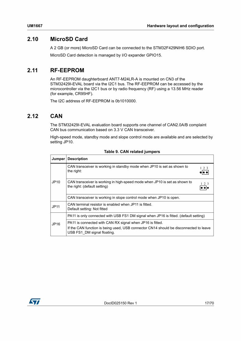
2.10 MicroSD Card . . . . . . . . . . . . . . . . . . . . . . . . . . . . . . . . . . . . . . . . . . . . . . 17
2.11 RF-EEPROM . . . . . . . . . . . . . . . . . . . . . . . . . . . . . . . . . . . . . . . . . . . . . . 17
2.12 CAN . . . . . . . . . . . . . . . . . . . . . . . . . . . . . . . . . . . . . . . . . . . . . . . . . . . . . 17
2.13 Ethernet . . . . . . . . . . . . . . . . . . . . . . . . . . . . . . . . . . . . . . . . . . . . . . . . . . 18
2.14 Extension connector . . . . . . . . . . . . . . . . . . . . . . . . . . . . . . . . . . . . . . . . . 18
2.15 Memories . . . . . . . . . . . . . . . . . . . . . . . . . . . . . . . . . . . . . . . . . . . . . . . . . 19
2.16 Analog input . . . . . . . . . . . . . . . . . . . . . . . . . . . . . . . . . . . . . . . . . . . . . . . 19
2.17 Camera module . . . . . . . . . . . . . . . . . . . . . . . . . . . . . . . . . . . . . . . . . . . . 19
2.18 Display and input devices . . . . . . . . . . . . . . . . . . . . . . . . . . . . . . . . . . . . . 20
2.19 Motor control . . . . . . . . . . . . . . . . . . . . . . . . . . . . . . . . . . . . . . . . . . . . . . 21
3 Connectors . . . . . . . . . . . . . . . . . . . . . . . . . . . . . . . . . . . . . . . . . . . . . . . 24
3.1 Motor control connector CN1 . . . . . . . . . . . . . . . . . . . . . . . . . . . . . . . . . . 24
3.2 Extension connector CN2 . . . . . . . . . . . . . . . . . . . . . . . . . . . . . . . . . . . . . 25
3.3 RF-EEPROM daughterboard connector CN3 . . . . . . . . . . . . . . . . . . . . . 26

DocID025150 Rev 1 3/70
UM1667 Contents
3
3.4 Analog input connector CN4 . . . . . . . . . . . . . . . . . . . . . . . . . . . . . . . . . . 26
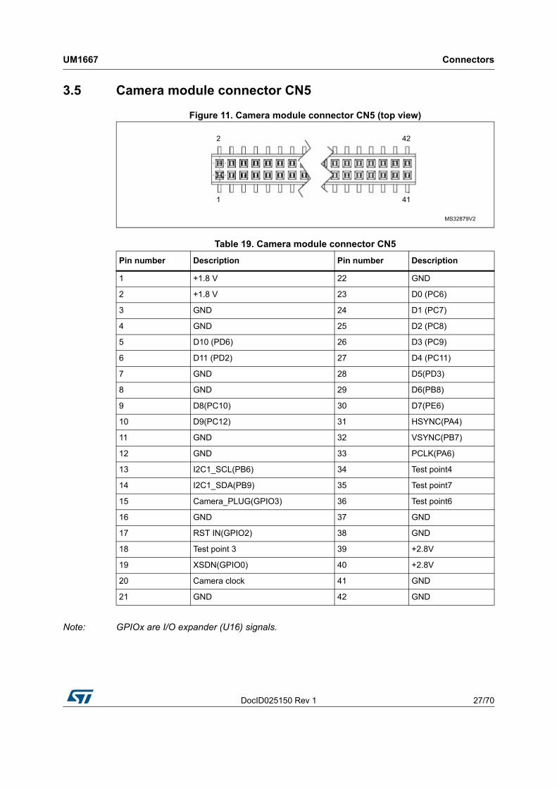
3.5 Camera module connector CN5 . . . . . . . . . . . . . . . . . . . . . . . . . . . . . . . . 27
3.6 Daughterboard extension connector CN6 and CN7 . . . . . . . . . . . . . . . . . 28
3.7 RS-232 connector CN8 . . . . . . . . . . . . . . . . . . . . . . . . . . . . . . . . . . . . . . 33
3.8 USB OTG2 HS Micro-AB connector CN9 . . . . . . . . . . . . . . . . . . . . . . . . 33
3.9 Ethernet RJ45 connector CN10 . . . . . . . . . . . . . . . . . . . . . . . . . . . . . . . . 34
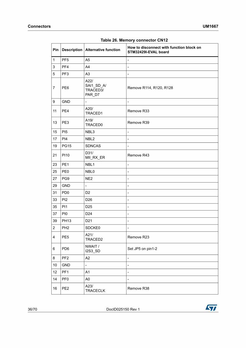
3.10 Memory connectors CN11 and CN12 . . . . . . . . . . . . . . . . . . . . . . . . . . . . 34
3.11 ETM trace debugging connector CN13 . . . . . . . . . . . . . . . . . . . . . . . . . . 37
3.12 USB OTG1 FS Micro-AB connector CN14 . . . . . . . . . . . . . . . . . . . . . . . . 38
3.13 USB OTG2 FS Micro-AB connector CN15 . . . . . . . . . . . . . . . . . . . . . . . . 38
3.14 JTAG/SWD connector CN16 . . . . . . . . . . . . . . . . . . . . . . . . . . . . . . . . . . 39
3.15 MicroSD connector CN17 . . . . . . . . . . . . . . . . . . . . . . . . . . . . . . . . . . . . . 39
3.16 Power connector CN18 . . . . . . . . . . . . . . . . . . . . . . . . . . . . . . . . . . . . . . 40
3.17 ST-LINK/V2 programming connector CN19 . . . . . . . . . . . . . . . . . . . . . . . 40
3.18 TFT LCD connector CN20 . . . . . . . . . . . . . . . . . . . . . . . . . . . . . . . . . . . . 40
3.19 ST-LINK/V2 USB Type B connector CN21 . . . . . . . . . . . . . . . . . . . . . . . . 41
3.20 CAN D-type 9-pin male connector CN22 . . . . . . . . . . . . . . . . . . . . . . . . . 41
3.21 Audio jack CN23 . . . . . . . . . . . . . . . . . . . . . . . . . . . . . . . . . . . . . . . . . . . . 41
3.22 Audio terminal CN24 . . . . . . . . . . . . . . . . . . . . . . . . . . . . . . . . . . . . . . . . 42
3.23 ST-LINK/V2 programming Tag-connector CN25 . . . . . . . . . . . . . . . . . . . 42
4 Schematics . . . . . . . . . . . . . . . . . . . . . . . . . . . . . . . . . . . . . . . . . . . . . . . 43
Appendix A STM32429I-EVAL I/O assignment . . . . . . . . . . . . . . . . . . . . . . . . . . . 61
Appendix B Mechanical dimensions. . . . . . . . . . . . . . . . . . . . . . . . . . . . . . . . . . . 68
Revision history . . . . . . . . . . . . . . . . . . . . . . . . . . . . . . . . . . . . . . . . . . . . . . . . . . . . 69

List of tables UM1667
4/70 DocID025150 Rev 1
List of tables
Table 1. Third-party toolchains . . . . . . . . . . . . . . . . . . . . . . . . . . . . . . . . . . . . . . . . . . . . . . . . . . . . . 10Table 2. Power related jumpers . . . . . . . . . . . . . . . . . . . . . . . . . . . . . . . . . . . . . . . . . . . . . . . . . . . . 11Table 3. 32.786 KHz crystal X1 related solder bridges. . . . . . . . . . . . . . . . . . . . . . . . . . . . . . . . . . . 13Table 4. 25 MHz crystal X2 related solder bridges . . . . . . . . . . . . . . . . . . . . . . . . . . . . . . . . . . . . . . 13Table 5. Boot related switches . . . . . . . . . . . . . . . . . . . . . . . . . . . . . . . . . . . . . . . . . . . . . . . . . . . . . 14Table 6. Audio related jumpers. . . . . . . . . . . . . . . . . . . . . . . . . . . . . . . . . . . . . . . . . . . . . . . . . . . . . 15Table 7. USB OTG2 configuration . . . . . . . . . . . . . . . . . . . . . . . . . . . . . . . . . . . . . . . . . . . . . . . . . . 16Table 8. RS-232 & IrDA related jumper . . . . . . . . . . . . . . . . . . . . . . . . . . . . . . . . . . . . . . . . . . . . . . 16Table 9. CAN related jumpers . . . . . . . . . . . . . . . . . . . . . . . . . . . . . . . . . . . . . . . . . . . . . . . . . . . . . 17Table 10. Ethernet related jumper . . . . . . . . . . . . . . . . . . . . . . . . . . . . . . . . . . . . . . . . . . . . . . . . . . . 18Table 11. Ethernet related solder bridges. . . . . . . . . . . . . . . . . . . . . . . . . . . . . . . . . . . . . . . . . . . . . . 18Table 12. NOR Flash related jumpers . . . . . . . . . . . . . . . . . . . . . . . . . . . . . . . . . . . . . . . . . . . . . . . . 19Table 13. LCD modules connector (CN20). . . . . . . . . . . . . . . . . . . . . . . . . . . . . . . . . . . . . . . . . . . . . 20Table 14. Motor control related solder bridges . . . . . . . . . . . . . . . . . . . . . . . . . . . . . . . . . . . . . . . . . . 23Table 15. Motor control connector CN1 . . . . . . . . . . . . . . . . . . . . . . . . . . . . . . . . . . . . . . . . . . . . . . . 24Table 16. Extension connector CN2 . . . . . . . . . . . . . . . . . . . . . . . . . . . . . . . . . . . . . . . . . . . . . . . . . . 25Table 17. RF-EEPROM daughterboard connector CN3. . . . . . . . . . . . . . . . . . . . . . . . . . . . . . . . . . . 26Table 18. Analog input-output connector CN4 . . . . . . . . . . . . . . . . . . . . . . . . . . . . . . . . . . . . . . . . . . 26Table 19. Camera module connector CN5 . . . . . . . . . . . . . . . . . . . . . . . . . . . . . . . . . . . . . . . . . . . . . 27Table 20. Daughterboard extension connector CN6 . . . . . . . . . . . . . . . . . . . . . . . . . . . . . . . . . . . . . 28Table 21. Daughterboard extension connector CN7 . . . . . . . . . . . . . . . . . . . . . . . . . . . . . . . . . . . . . 30Table 22. RS-232 connector CN8 with ISP support . . . . . . . . . . . . . . . . . . . . . . . . . . . . . . . . . . . . . . 33Table 23. USB OTG HS Micro-AB connector CN9. . . . . . . . . . . . . . . . . . . . . . . . . . . . . . . . . . . . . . . 33Table 24. RJ45 connector CN10 . . . . . . . . . . . . . . . . . . . . . . . . . . . . . . . . . . . . . . . . . . . . . . . . . . . . 34Table 25. Memory connector CN11 . . . . . . . . . . . . . . . . . . . . . . . . . . . . . . . . . . . . . . . . . . . . . . . . . . 34Table 26. Memory connector CN12 . . . . . . . . . . . . . . . . . . . . . . . . . . . . . . . . . . . . . . . . . . . . . . . . . . 36Table 27. ETM trace debugging connector CN13 . . . . . . . . . . . . . . . . . . . . . . . . . . . . . . . . . . . . . . . 37Table 28. USB OTG1 FS Micro-AB connector CN14 . . . . . . . . . . . . . . . . . . . . . . . . . . . . . . . . . . . . . 38Table 29. USB OTG2 FS Micro-AB connector CN15 . . . . . . . . . . . . . . . . . . . . . . . . . . . . . . . . . . . . . 38Table 30. JTAG/SWD debugging connector CN15 . . . . . . . . . . . . . . . . . . . . . . . . . . . . . . . . . . . . . . 39Table 31. MicroSD connector CN17 . . . . . . . . . . . . . . . . . . . . . . . . . . . . . . . . . . . . . . . . . . . . . . . . . . 40Table 32. USB type B connector CN21 . . . . . . . . . . . . . . . . . . . . . . . . . . . . . . . . . . . . . . . . . . . . . . . 41Table 33. CAN D-type 9-pin male connector CN22 . . . . . . . . . . . . . . . . . . . . . . . . . . . . . . . . . . . . . . 41Table 34. Audio terminal CN24. . . . . . . . . . . . . . . . . . . . . . . . . . . . . . . . . . . . . . . . . . . . . . . . . . . . . . 42Table 35. STM32429I-EVAL I/O assignment . . . . . . . . . . . . . . . . . . . . . . . . . . . . . . . . . . . . . . . . . . . 61Table 36. Mechanical dimensions . . . . . . . . . . . . . . . . . . . . . . . . . . . . . . . . . . . . . . . . . . . . . . . . . . . 68Table 37. Document revision history . . . . . . . . . . . . . . . . . . . . . . . . . . . . . . . . . . . . . . . . . . . . . . . . . 69

DocID025150 Rev 1 5/70
UM1667 List of figures
5
List of figures
Figure 1. STM32429I-EVAL evaluation board . . . . . . . . . . . . . . . . . . . . . . . . . . . . . . . . . . . . . . . . . . 1Figure 2. Hardware block diagram . . . . . . . . . . . . . . . . . . . . . . . . . . . . . . . . . . . . . . . . . . . . . . . . . . . 8Figure 3. Evaluation board layout . . . . . . . . . . . . . . . . . . . . . . . . . . . . . . . . . . . . . . . . . . . . . . . . . . . . 9Figure 4. Orientation setting of 4.3 inch LCD daughterboard . . . . . . . . . . . . . . . . . . . . . . . . . . . . . . 21Figure 5. PCB underside rework for motor control . . . . . . . . . . . . . . . . . . . . . . . . . . . . . . . . . . . . . . 22Figure 6. PCB topside rework for motor control . . . . . . . . . . . . . . . . . . . . . . . . . . . . . . . . . . . . . . . . . 22Figure 7. Motor control connector CN1 (top view) . . . . . . . . . . . . . . . . . . . . . . . . . . . . . . . . . . . . . . . 24Figure 8. Extension connector CN2 top view. . . . . . . . . . . . . . . . . . . . . . . . . . . . . . . . . . . . . . . . . . . 25Figure 9. RF-EEPROM daughterboard connector CN3 (front view) . . . . . . . . . . . . . . . . . . . . . . . . . 26Figure 10. Analog input-output connector CN4 (top view) . . . . . . . . . . . . . . . . . . . . . . . . . . . . . . . . . . 26Figure 11. Camera module connector CN5 (top view). . . . . . . . . . . . . . . . . . . . . . . . . . . . . . . . . . . . . 27Figure 12. RS-232 connector (front view) . . . . . . . . . . . . . . . . . . . . . . . . . . . . . . . . . . . . . . . . . . . . . . 33Figure 13. USB OTG2 HS Micro-AB connector CN9 (front view) . . . . . . . . . . . . . . . . . . . . . . . . . . . . 33Figure 14. Ethernet RJ45 connector CN10 (front view) . . . . . . . . . . . . . . . . . . . . . . . . . . . . . . . . . . . . 34Figure 15. ETM trace debugging connector CN13 (top view) . . . . . . . . . . . . . . . . . . . . . . . . . . . . . . . 37Figure 16. USB OTG1 FS Micro-AB connector CN14 (front view). . . . . . . . . . . . . . . . . . . . . . . . . . . . 38Figure 17. USB OTG2 FS Micro-AB connector CN15 (front view). . . . . . . . . . . . . . . . . . . . . . . . . . . . 38Figure 18. JTAG/SWD debugging connector CN16 (top view) . . . . . . . . . . . . . . . . . . . . . . . . . . . . . . 39Figure 19. MicroSD connector CN17 (front view) . . . . . . . . . . . . . . . . . . . . . . . . . . . . . . . . . . . . . . . . 39Figure 20. Power supply connector CN18 . . . . . . . . . . . . . . . . . . . . . . . . . . . . . . . . . . . . . . . . . . . . . . 40Figure 21. USB type B connector CN21 (front view) . . . . . . . . . . . . . . . . . . . . . . . . . . . . . . . . . . . . . . 41Figure 22. CAN D-type 9-pin male connector CN22 (front view) . . . . . . . . . . . . . . . . . . . . . . . . . . . . . 41Figure 23. Audio terminal CN24 (front view) . . . . . . . . . . . . . . . . . . . . . . . . . . . . . . . . . . . . . . . . . . . . 42Figure 24. STM32429I-EVAL. . . . . . . . . . . . . . . . . . . . . . . . . . . . . . . . . . . . . . . . . . . . . . . . . . . . . . . . 43Figure 25. MCU . . . . . . . . . . . . . . . . . . . . . . . . . . . . . . . . . . . . . . . . . . . . . . . . . . . . . . . . . . . . . . . . . . 44Figure 26. Power . . . . . . . . . . . . . . . . . . . . . . . . . . . . . . . . . . . . . . . . . . . . . . . . . . . . . . . . . . . . . . . . . 45Figure 27. SRAM, Flash and SDRAM . . . . . . . . . . . . . . . . . . . . . . . . . . . . . . . . . . . . . . . . . . . . . . . . . 46Figure 28. Audio. . . . . . . . . . . . . . . . . . . . . . . . . . . . . . . . . . . . . . . . . . . . . . . . . . . . . . . . . . . . . . . . . . 47Figure 29. LCD, camera and connectors . . . . . . . . . . . . . . . . . . . . . . . . . . . . . . . . . . . . . . . . . . . . . . . 48Figure 30. Ethernet . . . . . . . . . . . . . . . . . . . . . . . . . . . . . . . . . . . . . . . . . . . . . . . . . . . . . . . . . . . . . . . 49Figure 31. USB OTG HS . . . . . . . . . . . . . . . . . . . . . . . . . . . . . . . . . . . . . . . . . . . . . . . . . . . . . . . . . . . 50Figure 32. USB OTG FS . . . . . . . . . . . . . . . . . . . . . . . . . . . . . . . . . . . . . . . . . . . . . . . . . . . . . . . . . . . 51Figure 33. RS-232 and IrDA . . . . . . . . . . . . . . . . . . . . . . . . . . . . . . . . . . . . . . . . . . . . . . . . . . . . . . . . 52Figure 34. CAN, MicroSD Card and IO expander . . . . . . . . . . . . . . . . . . . . . . . . . . . . . . . . . . . . . . . . 53Figure 35. Peripherals . . . . . . . . . . . . . . . . . . . . . . . . . . . . . . . . . . . . . . . . . . . . . . . . . . . . . . . . . . . . . 54Figure 36. Motor control . . . . . . . . . . . . . . . . . . . . . . . . . . . . . . . . . . . . . . . . . . . . . . . . . . . . . . . . . . . . 55Figure 37. Extension connector . . . . . . . . . . . . . . . . . . . . . . . . . . . . . . . . . . . . . . . . . . . . . . . . . . . . . . 56Figure 38. ST-LINK/V2. . . . . . . . . . . . . . . . . . . . . . . . . . . . . . . . . . . . . . . . . . . . . . . . . . . . . . . . . . . . . 57Figure 39. JTAG and trace. . . . . . . . . . . . . . . . . . . . . . . . . . . . . . . . . . . . . . . . . . . . . . . . . . . . . . . . . . 58Figure 40. 4.3' TFT LCD daughter board MB1046. . . . . . . . . . . . . . . . . . . . . . . . . . . . . . . . . . . . . . . . 59Figure 41. Camera daughterboard MB1066 . . . . . . . . . . . . . . . . . . . . . . . . . . . . . . . . . . . . . . . . . . . . 60Figure 42. Mechanical dimensions . . . . . . . . . . . . . . . . . . . . . . . . . . . . . . . . . . . . . . . . . . . . . . . . . . . 68

Overview UM1667
6/70 DocID025150 Rev 1
1 Overview
1.1 Features
• STM32F429NIH6 microcontroller
• Six 5 V power supply options:
– Power jack
– ST-LINK/V2 USB connector
– User USB HS connector
– User USB FS1 connector
– User USB FS2 connector
– Daughterboard
• SAI Audio DAC, stereo audio jack which supports headset with microphone
• Stereo digital microphone, audio terminal connector used to connect external speakers
• 2 GByte (or more) SDIO interface MicroSD Card
• RF-EEPROM on I2C compatible serial interface
• RS-232 communication
• IrDA transceiver
• JTAG/SWD and ETM trace debug support, ST-LINK/V2 embedded
• IEEE-802.3-2002 compliant Ethernet connector
• Camera module
• 8 M x 32-bit SDRAM, 1 M x 16-bit SRAM & 8 M x 16-bit NOR Flash
• 4.3 inch 480 x 272 pixel TFT LCD with resistive touch panel
• Joystick with 4-direction control and selector
• Reset, WakeUp, Tamper or key button
• 4 user color LEDs
• Extension connectors & memory connectors for daughterboard or wrapping board
• USB OTG HS and FS with Micro-AB connectors
• RTC with backup battery
• CAN2.0A/B compliant connection
• Potentiometer
• Motor control connector
1.2 Demonstration software
Demonstration software is preloaded in the Flash memory of the board for easy demonstration of the device peripherals in stand-alone mode. For more information and to download the latest version, refer to the STM32429I-EVAL demonstration software on www.st.com.

DocID025150 Rev 1 7/70
UM1667 Overview
69
1.3 Order code
To order the evaluation board based on STM32F429NIH6 MCU and 4.3” TFT LCD, use the order code:STM32429I-EVAL1.
1.4 Delivery recommendations
Some verifications are needed before using the board for the first time to make sure that nothing was damaged during shipment and that no components are unplugged or lost.
When the board is extracted from its plastic bag, please check that no component remains in the bag.
The main components to verify are:
1. The 25 MHz crystal (X2) & 25 MHz crystal (X4) which may have been removed by a shock from its socket.
2. The MicroSD Card which may have been ejected from the connector CN17 (right side of the board).
3. The dual-interface EEPROM board (ANT7-M24LR-A) which may have been unplugged from the connector CN3 (top left corner of the board).
4. The camera module on the camera daughterboard (MB1066) which may have been unplugged.
Warning: There is an explosion risk if the battery is replaced by an incorrect one. Make sure to dispose of used batteries according to the instructions.

Hardware layout and configuration UM1667
8/70 DocID025150 Rev 1
2 Hardware layout and configuration
The STM32429I-EVAL evaluation board is designed around the STM32F429NIH6 (216-pin TFBGA package).
The hardware block diagram Figure 2 illustrates the connection between the STM32F429NIH6 and peripherals (SDRAM, SRAM, NOR Flash, camera module, color LCD, USB OTG connectors, motor control connector, USART, IrDA, ethernet, audio, CAN, RF-EEPROM, MicroSD Card and embedded ST-LINK) and Figure 3 will help the user to locate these features on the actual evaluation board.
Figure 2. Hardware block diagram

DocID025150 Rev 1 9/70
UM1667 Hardware layout and configuration
69
Figure 3. Evaluation board layout

Hardware layout and configuration UM1667
10/70 DocID025150 Rev 1
2.1 Development and debug support
Version 2 of the ST-LINK (ST-LINK/V2) is embedded on the board. This tool allows on-board program loading and debugging of the STM32 using a JTAG or SWD interface. Third-party debug tools are also supported by the JTAG/SWD connector, CN16, and ETM Trace connector, CN13.
A specific driver must be installed by the user on his PC to communicate with the embedded ST-LINK/V2. An install shield called ST-LINK_V2_USBdriver.exe is available on the web. To download and install this driver, refer to the Software and development tools page for STM32 on www.st.com.
Third-party toolchains, ARM® Atollic® TrueSTUDIO®, KEILTM MDK-ARMTM, IAR EWARM®and Altium®, TASKING™ VX-Toolset support ST-LINK/V2 according to the following table:
The embedded ST-LINK/V2 is connected to the PC via a standard USB cable connected to connector CN21. The bicolor LED LD11 (COM) indicates the status of the communication as follows:
• Red LED slow blinking/Off: At power on before USB initialization
• Red LED fast blinking/Off: After the first correct communication between PC and ST-Link/V2 (enumeration)
• Red LED On: When initialization between PC and ST-LINK/V2 is successfully finished
• Green LED On: After successful target communication initialization
• Red/Green LED blinking: During communication with target
• Red LED On: Communication finished and OK
• Orange LED On: Communication failure
Note: The board can be powered via CN21 (embedded ST-LINK/V2 USB connector) even if an external tool is connected to CN13 (ETM trace connector) or CN16 (external JTAG & SWD connector).
By default ETM only works at 50 MHz clock because ETM signals are shared with other peripherals. If best performance of ETM is required (90 MHz), then R29, R32, R34, R36, R40, R114 and R120 must be removed to reduce the stub on ETM signals. In this case SAI and camera are not functional and NOR Flash and SRAM's addresses are limited on A18.
Caution: When an external high speed debug tool connected to CN13 or CN16 is used for program loading or debugging, it is recommended to remove ESD protections D9 to D13 connected on JTAG signals.
Table 1. Third-party toolchains
Third-party Toolchain Version
ARM Atollic TrueSTUDIO 2.1
IAR EWARM 6.20
Keil MDK-ARM 4.20
Altium Tasking VX-Toolset 4.0.1

DocID025150 Rev 1 11/70
UM1667 Hardware layout and configuration
69
2.2 Power supply
The STM32429I-EVAL evaluation board is designed to be powered by a 5 V DC power supply and is protected by PolyZen from a wrong power plug-in event. It is possible to configure the evaluation board to use any of following six sources for the power supply:
• 5 V DC power adapter connected to CN18, the power jack on the board (Power Supply Unit on silk screen of JP12(E5V)).
• 5 V DC power with 500 mA limitation from CN21, the USB type B connector of ST-LINK/V2 (USB 5 V power source on silkscreen of JP12(STlk)).
• 5 V DC power with 500 mA limitation from CN9, the USB OTG2 HS Micro-AB connector (USB 5V power source on silkscreen of JP12 (HS)).
• 5 V DC power with 500 mA limitation from CN14, the USB OTG1 FS Micro-AB connector (USB 5V power source on silkscreen of JP12 (FS1)).
• 5 V DC power with 500 mA limitation from CN15, the USB OTG2 FS Micro-AB connector (USB 5 V power source on silkscreen of JP12 (FS2)).
• 5 V DC power from CN6 & CN7, the extension connectors for daughterboard (Daughterboard power source on silkscreen of JP12 (D5V)).
The power supply is configured by setting the related jumpers JP2, JP8 and JP12 as described in Table 2.
Table 2. Power related jumpers
Jumper Description
JP2JP2 is used to measure MCU current consumption manually by multimeter.
Default setting: Fitted
JP8
Vbat is connected to +3.3V when JP8 is set as shown to the right: (Default setting)
Vbat is connected to battery when JP8 is set as shown to the right:
JP12
(continued on next page)
JP12 is used to select one of the six possible power supply resources.
For power supply from USB connector of ST-LINK/V2 (CN21) to STM32429I-EVAL only, JP12 is set as shown to the right: (Default setting)
For power supply jack (CN18) to the STM32429I-EVAL only, JP12 is set as shown to the right:
For power supply from the daughterboard connectors (CN6 & CN7) to STM32429I-EVAL only, JP12 is set as shown to the right:
1 2 3
1 2 3

Hardware layout and configuration UM1667
12/70 DocID025150 Rev 1
The LED LD10 is lit when the STM32429I-EVAL evaluation board is powered by the 5 V correctly.
Note: In order to avoid the impact of USB PHY and Ethernet PHY and get precise results of current consumption on JP2, the following configurations must be implemented:
• Configure Ethernet PHY in Power Down Mode by setting low level of IO_Expander (EXP_IO1).
• Configure USB HS PHY in Low Power Mode (Register Address=04,bit 6 in USB PHY).
JP12 (continued)
For power supply from USB OTG2 FS (CN15) to STM32429I-EVAL only, JP12 is set as shown to the right:
For power supply from USB OTG1 FS (CN14) to STM32429I-EVAL only, JP12 is set as shown to the right:
For power supply from USB OTG2 HS (CN9) to STM32429I-EVAL only, JP12 is set as shown to the right:
For power supply from power supply jack(CN18) to both STM32429I-EVAL and daughterboard connected on CN6 & CN7, JP12 is set as shown to the right (daughterboard must not have its own power supply connected)
Table 2. Power related jumpers (continued)
Jumper Description

DocID025150 Rev 1 13/70
UM1667 Hardware layout and configuration
69
2.3 Clock source
Two clock sources are available on the STM32429I-EVAL evaluation board for the STM32F429NIH6 and embedded RTC.
The camera module, ethernet PHY and USB PHY on the STM32429I-EVAL evaluation board have their own clock sources.
• X1, 32.768 KHz crystal for embedded RTC.
• X2, 25 MHz crystal with socket for STM32F429NIH6 microcontroller, it can be removed from the socket when an internal RC clock is used.
• X3, 24 MHz oscillator for camera module.
• X4, 25 MHz crystal with socket for ethernet PHY.
• X5, 24 MHz crystal for USB OTG2 HS PHY.
Jumper JP6 for Ethernet clock refer to Section 2.13.
2.4 Reset source
The reset signal of STM32429I-EVAL evaluation board is low active. Reset sources include:
• Reset button B1
• Debugging tools from JTAG/SWD connector CN16 and ETM trace connector CN13
• Daughterboard from CN6
• Embedded ST-LINK/V2
Table 3. 32.786 KHz crystal X1 related solder bridges
Solder bridge Description
SB3
PC14 is connected to 32.786 KHz crystal when SB3 is open. (Default setting)
PC14 is connected to extension connector CN7 when SB3 is closed. In such case R19 must be removed to avoid disturbance due to the 32.786 KHz quartz.
SB4
PC15 is connected to 32.786 KHz crystal when SB4 is open. (Default setting)
PC15 is connected to extension connector CN7 when SB4 is closed. In such case R18 must be removed to avoid disturbance due to the 32.786 KHz quartz.
Table 4. 25 MHz crystal X2 related solder bridges
Solder bridge Description
SB5
PH0 is connected to 25 MHz crystal when SB5 is open. (Default setting)
PH0 is connected to extension connector CN6 when SB5 is closed. In such case R20 must be removed to avoid disturbance due to the 25 MHz quartz
SB6
PH1 is connected to 25 MHz crystal when SB6 is open (Default setting).
PH1 is connected to extension connector CN7 when SB6 is closed. In such case C23 & X2 must be removed to avoid disturbance due to the 25 MHz quartz.

Hardware layout and configuration UM1667
14/70 DocID025150 Rev 1
2.5 Boot option
The STM32429I-EVAL evaluation board can boot from:
• Embedded user Flash
• System memory with boot loader for ISP
• Embedded SRAM for debugging
The boot option is configured by setting switch SW1 (BOOT0) and SW2 (BOOT1).
Note: The RS-232 boot loader mechanism is not supported on the STM32429I-EVAL.
2.6 Audio
An audio codec WM8994ECS/R with 4 DACs and 2 ADCs inside is connected to the SAI interface of the STM32F429NIH6 to support the TDM feature on the SAI port. This feature implements audio recording on digital and analog microphone, and audio playback of different audio streams on headphone and line-out at the same time.
It communicates with the STM32F429NIH6 via the I2C1 bus which is shared with the LCD, camera module, RF-EEPROM, IO expander and CN2 connector.
The analog microphone on the headset is connected to the ADC of WM8994ECS/R. External speakers can be connected to WM8994ECS/R via audio terminal connector CN24.
There are two digital microphones (MEMs microphone) MP34DT01TR on the STM32429I-EVAL evaluation board. They can be connected to either audio codec or the I2S port of STM32F429NIH6 by setting jumpers as shown in Table 6.
Table 5. Boot related switches
Switch Boot description Switch configuration
SW1 & SW2
STM32429I-EVAL boots from User Flash when SW1 is set as shown to the right. SW2 is not required in this configuration. (Default setting)
STM32429I-EVAL boots from Embedded SRAM when SW1 and SW2 are set as shown to the right.
STM32429I-EVAL boots from System Memory when SW1 and SW2 are set as shown to the right.
0 < > 1
SW
0 < > 1
SW1
SW2
0 < > 1
SW
SW

DocID025150 Rev 1 15/70
UM1667 Hardware layout and configuration
69
Note: The I2C address of WM8994ECS/R is 0b0011010.
2.7 USB OTG1 FS
The STM32429I-EVAL evaluation board supports USB OTG1 full speed communication via a USB Micro-AB connector (CN14) and USB power switch (U9) connected to VBUS. The evaluation board can be powered by this USB connection at 5 V DC with a 500 mA current limitation.
Green LED LD7 will be lit in one of these cases:
• Power switch (U9) is ON and the STM32429I-EVAL is acting as a USB host.
• VBUS is powered by another USB host and the STM32429I-EVAL is acting as a USB device.
Red LED LD8 will be lit when over-current occurs.
JP16 must be removed when using USB OTG FS as mentioned in Table 9.
Table 6. Audio related jumpers
Jumper Description
JP14
Data signal on digital microphone is connected to audio codec when JP14 is set as shown to the right (Default setting)
Data signal on digital microphone is connected to I2S port of STM32F429NIH6 when JP14 is set as shown to the right (also need to set JP5 according to this table)
JP15
Clock signal on digital microphone is connected to audio codec when JP15 is set as shown to the right (Default setting)
Clock signal on digital microphone is connected to Timer output (PC7) of STM32F429NIH6 when JP15 is set as shown to the right (also need to set JP4 according to this table)
JP4
PB4 is as TDO/SWO signal when JP4 is set as shown to the right (Default setting)
PB4 is connected to Timer input(PC6) of STM32F429NIH6 as I2S clock signal when JP4 is set as shown to the right (also need to set JP15 according to this table)
JP5
PD6 is as FMC_NWAIT signal when JP5 is set as shown to the right (Default setting)
PD6 is connected to digital microphone as I2S data signal when JP5 is set as shown to the right (also need to set JP14 according to this table):
JP13
Digital microphone power source is connected to +3.3V power when JP13 is set as shown to the right
Digital microphone power source is connected to MICBIAS1 from WM8994ECS/R when JP13 is set as shown to the right. MICBIAS1 setting is requested by digital microphone connected to Codec. (Default setting)
1 2 3
1 2 3
1 2 3
1 2 3
1 2 3
1 2 3
1 2 3
1 2 3
1 2 3
1 2 3

Hardware layout and configuration UM1667
16/70 DocID025150 Rev 1
2.8 USB OTG2 HS & FS
The STM32429I-EVAL evaluation board supports USB OTG2:
• High speed communication via USB Micro-AB connector (CN9), USB high speed PHY (U7) for high speed function
• Full speed communication via USB Micro-AB connector (CN15)
The evaluation board can be powered by these USB connectors (CN9 or CN15) at 5 V DC with a 500 mA current limitation.
Some OTG2 FS signals are shared with the OTG2 HS ULPI bus, so some PCB rework is needed when using OTG2 FS (CN15) as shown in Table 7.
A USB power switch (U6) is connected on VBUS and provides power to either:
• CN9 (with R81 & R97 mounted and R83 & R95 un-mounted)
• CN15 (with R83 & R95 mounted and R81& R97 un-mounted)
Green LED LD5 (for CN9) or LD9 (for CN15) will be lit when either:
• Power switch (U6) is ON and STM32429I-EVAL is acting as a USB host.
• VBUS is powered by another USB host, and STM32429I-EVAL is acting as a USB device.
Red LED LD6 is lit if over-current occurs.
2.9 RS-232 & IrDA
RS-232 and IrDA communication is supported by 9-pin RS-232 D-type connector, CN8, and IrDA transceiver, U1, which is connected to USART1 of the STM32F429NIH6 on the STM32429I-EVAL evaluation board.
Table 7. USB OTG2 configuration
Function Mount Remove
OTG2 HS-CN9 (Default) R108, R112, R81,R97 R260, R264, R83,R95
OTG2 FS-CN15 R260, R264, R83,R95 R108, R112, R81,R97
Table 8. RS-232 & IrDA related jumper
Jumper Description
JP7
USART1_RX is connected to RS-232 transceiver and RS-232 communication is enabled when JP7 is set as shown to the right (Default setting):
USART1_RX is connected to IrDA transceiver and IrDA communication is enabled when JP7 is set as shown to the right:
1 2 3
1 2 3
DocID025150 Rev 1 17/70
UM1667 Hardware layout and configuration
69
2.10 MicroSD Card
A 2 GB (or more) MicroSD Card can be connected to the STM32F429NIH6 SDIO port.
MicroSD Card detection is managed by I/O expander GPIO15.
2.11 RF-EEPROM
An RF-EEPROM daughterboard ANT7-M24LR-A is mounted on CN3 of the STM32429I-EVAL board via the I2C1 bus. The RF-EEPROM can be accessed by the microcontroller via the I2C1 bus or by radio frequency (RF) using a 13.56 MHz reader (for example, CR95HF).
The I2C address of RF-EEPROM is 0b1010000.
2.12 CAN
The STM32429I-EVAL evaluation board supports one channel of CAN2.0A/B complaint CAN bus communication based on 3.3 V CAN transceiver.
High-speed mode, standby mode and slope control mode are available and are selected by setting JP10.
Table 9. CAN related jumpers
Jumper Description
JP10
CAN transceiver is working in standby mode when JP10 is set as shown to the right:
CAN transceiver is working in high-speed mode when JP10 is set as shown to the right: (default setting)
CAN transceiver is working in slope control mode when JP10 is open.
JP11CAN terminal resistor is enabled when JP11 is fitted. Default setting: Not fitted
JP16
PA11 is only connected with USB FS1 DM signal when JP16 is fitted. (default setting)
PA11 is connected with CAN RX signal when JP16 is fitted.
If the CAN function is being used, USB connector CN14 should be disconnected to leave USB FS1_DM signal floating.
1 2 3
1 2 3

Hardware layout and configuration UM1667
18/70 DocID025150 Rev 1
2.13 Ethernet
The STM32429I-EVAL evaluation board supports 10M/100M Ethernet communication by a PHY DP83848CVV (U5) and integrated RJ45 connector (CN10). Ethernet PHY is connected to the STM32F429NIH6 via the MII interface.
A 25 MHz clock can be generated by PHY or provided by MCO from the STM32F429NIH6 by setting jumper JP6 as shown in Table 10.
Note: Ethernet works properly in the default setting (which RX_ER is not connected to PI10 of STM32F429NIH6) because PI10 is shared with data signal of SDRAM. If RX_ER signal is needed, remove R244 and solder R43.
2.14 Extension connector
An extension connector (CN2) is intended for external board connection to the STM32429I-EVAL evaluation board using cable FFSD-05-D-04.00-01-N.
The external board can exchange data with the STM32F429NIH6 via the I2C1 or SPI3 ports.
Table 10. Ethernet related jumper
Jumper Description
JP6
25 MHz clock is provided by external Crystal X4 when JP5 is set as shown to the right: (Default setting)
25 MHz clock for MII is provided by MCO at PA8 when JP5 is set as shown to the right:
Table 11. Ethernet related solder bridges
Solder bridges Description
SB7MII CRS on DP83848CVV is connected to PA0 when SB7 is closed. PA0 is shared with Wakeup button and MC_ENA. Default setting: Open
SB8MII COL on DP83848CVV is connected to PH3 when SB8 is closed. PH3 is shared with SDRAM chip select SDNE0. Default setting: Open
1 2 3
1 2 3

DocID025150 Rev 1 19/70
UM1667 Hardware layout and configuration
69
2.15 Memories
8 M x 32-bit SDRAM is connected to SDRAM Bank1 of the STM32F429NIH6 FMC interface.
1 Mbit x 16 SRAM is connected to bank1 NOR/PSRAM2 of the FMC interface and both 8-bit and 16-bit access is allowed by BLN0 & BLN1 connected to BLE & BHE of SRAM respectively.
128 Mbit NOR Flash is connected to bank1 NOR/PSRAM1 of the FMC interface. The 16-bit operation mode is selected by the pull-up resistor connected to BYTE pin of NOR Flash. Write protection is enabled or disabled by the setting of jumper JP9:
All memory signals are also connected on memory connectors CN11 and CN12 for memory daughterboards.
Some limitations occur when using other peripherals:
1. FMC addressing limitation depending on number of trace data buses used (A18 max for 4-bit ETM to A21 max for 1-bit ETM).
2. NOR Flash addresses limited to A21 when SAI or camera module is used.
In such cases, memory addresses A18 to A21 not connected to FMC are pulled down so memories can be addressed within a limited address range. If A22 is required, the camera board should be removed and SAI1_SDA should be tri-stated. AIF1_TRI (address: 0x300) bit 13 of the W8994 can be used to tri-state ADCDAT1 pin (SAI1_SDA) when it is set to 1.
2.16 Analog input
The two-pin header CN4, and 10 Kohm potentiometer RV1, are connected to PF10 of the STM32F429NIH6 as analog input. A low pass filter can be implemented by replacing R27 and C24 with the resistor and capacitor requested by end user's application.
2.17 Camera module
Connector CN5 (for DCMI signals) on the STM32429I-EVAL evaluation board connects to the camera module daughterboard MB1066.
DCMI signals are duplicated with other peripherals (SAI, I2S, NOR Flash, MicroSD Card, Trace, Ethernet). These peripherals may not function correctly when the camera module is being used. To avoid SAI1_SDA signal impacting D7, SAI1_SDA should be tri-stated.
Refer to Section 2.15 to see how to tri-state SAI1_SDA.
Table 12. NOR Flash related jumpers
Jumper Description
JP9Write protection is enabled when JP9 is fitted while write protection is disabled when JP9 is not fitted. Default Setting: Not fitted
JP5 Description of JP5 is in Section 1.6: Audio

Hardware layout and configuration UM1667
20/70 DocID025150 Rev 1
2.18 Display and input devices
A 4.3 inch 480x272 TFT color LCD with resistive touch panel can be connected to the RGB LCD interface of STM32F429NIH6.
4 general purpose color LED's (LD 1,2,3,4) are available as display devices.
The 4-direction joystick (B4), Wakeup (B2) and Tamper/key button (B3) are available as input devices.
Table 13. LCD modules connector (CN20)
Pin No. Description Pin connection Pin No. Description Pin connection
1 GND - 2 GND -
3 R0 PI15 4 G0 PJ7
5 R1 PJ0 6 G1 PJ8
7 R2 PJ1 8 G2 PJ9
9 R3 PJ2 10 G3 PJ10
11 R4 PJ3 12 G4 PJ11
13 R5 PJ4 14 G5 PK0
15 R6 PJ5 16 G6 PK1
17 R7 PJ6 18 G7 PK2
19 GND - 20 GND -
21 B0 PJ12 22 ENB PK7
23 B1 PJ13 24 - -
25 B2 PJ14 26 HSYNC PI12
27 B3 PJ15 28 VSYNC PI13
29 B4 PK3 30 GND -
31 B5 PK4 32 CLK PI14
33 B6 PK5 34 GND -
35 B7 PK6 36 RESET# -
37 GND - 38 I2C1_SDA PB9
39 INT IO EXPANDER GPIO4 40 I2C1_SCL PB6
41 - - 42 - -
43 BL_CTRL PA8 44 - -
45 5V - 46 - -
47 BLGND - 48 - -
49 BLGND - 50 3.3V -

DocID025150 Rev 1 21/70
UM1667 Hardware layout and configuration
69
Note: On 4.3-inch daughterboard, BL_CTRL (PA8) can be used to manage on/off of backlight if needed.
Because BL_CTRL is shared with MII_MCO which is in default setting, R279 must be removed and R283 must be soldered with a 0 ohm resistor.
The orientation setting of 4.3 inch LCD daughterboard can be changed by hinged standoffs and pillars. There are two possible orientations according to holes on the motherboard and LCD daughterboard. Refer to Figure 4 for details.
Figure 4. Orientation setting of 4.3 inch LCD daughterboard
2.19 Motor control
The STM32429I-EVAL evaluation board supports both asynchronous and synchronous three-phase brushless motor control via a 34-pin connector, CN1, which provides all required control and feedback signals to and from motor power-driving board.
Available signals on this connector include emergency stop, motor speed, 3 phase motor current, bus voltage, heatsink temperature coming from the motor driving board and 6 channels of PWM control signal going to the motor driving circuit.
Some PCB rework is needed for motor control application to disconnect peripherals which share I/Os with motor control connector and connect these I/Os to Motor control connector.
• Remove R219, R214, R211, R227, R283, R279, R256, R261, R102, R104, R243, R222, R228, R238, R239, R267, R281, R249, SB7, JP4 (no jumper on pin 2-3), JP15 (no jumper on pin 2-3), JP16.
• Mount R16, R223, R210, R215, R225, R268, R255, R252, R282, R234, R240, R218, R232, R242, R235, R263, R292, R280, R246 with 0 ohm resistors.

Hardware layout and configuration UM1667
22/70 DocID025150 Rev 1
All resistors to be removed on the underside of the board are marked in red, while resistors to be soldered are marked in green in Figure 5.
Figure 6 shows all resistors to be removed on the topside of the board marked in red, while resistors to be soldered are marked in green (removal of R102 and R104, and mounting of R16).
Figure 5. PCB underside rework for motor control
Figure 6. PCB topside rework for motor control

DocID025150 Rev 1 23/70
UM1667 Hardware layout and configuration
69
Table 14. Motor control related solder bridges
Solder bridges Description
SB1
The special motor current sampling operation is enabled when SB1 is closed (PA12 connected to PA8). The I/O pins PA12 and PA8 are disconnected and can be used by a daughterboard when SB1 is not fitted.
Default setting: Open
SB2SB2 should be kept on open when encoder signal is from pin31 of motor control connector CN1, while it should be kept on close when analog signal is from pin31 of CN1 for a special motor.
Default setting: Open

Connectors UM1667
24/70 DocID025150 Rev 1
3 Connectors
3.1 Motor control connector CN1
Figure 7. Motor control connector CN1
Table 15. Motor control connector CN1
DescriptionSTM32F429NIH6 pin
CN1 pin number
CN1 pin number
STM32F429NIH6 pin
Description
Emergency stop PA6 1 2 - GND
MC_UH PC6 3 4 - GND
MC_UL PA7 5 6 - GND
MC_VH PC7 7 8 - GND
MC_VL PB0 9 10 - GND
MC_WH PC8 11 12 - GND
MC_WL PB1 13 14 PC4 Bus voltage
current A PC1 15 16 - GND
current B PC2 17 18 - GND
current C PC3 19 20 - GND
NTC bypass relay
PG11 21 22 - GND
Dissipative brake PWM
PB8 23 24 - GND
+5V power - 25 26 PC5Heatsink temperature
PFC syncPA12 & PA8. See Table 14 for detail
27 28 - 3.3V power
PFC PWM PA11 29 30 - GND
Encoder A PA0 31 32 - GND
Encoder B PA1 33 34 PA2Encoder Index

DocID025150 Rev 1 25/70
UM1667 Connectors
69
3.2 Extension connector CN2
Figure 8. Extension connector CN2 top view
Table 16. Extension connector CN2
Pin number Pin name I2C interface description SPI interface description
1 PB9 I2C1_SDA SPI3_CS
2 PC11 - SPI3_MISO
3 PB6 I2C1_SCL EXT_RESET
4 PC10 EXT_RESET SPI3_SCK
5 NC - -
6 PC12 - SPI3_MOSI
7 GND - -
8 +5V - -
9 NC - -
10 NC - -

Connectors UM1667
26/70 DocID025150 Rev 1
3.3 RF-EEPROM daughterboard connector CN3
Figure 9. RF-EEPROM daughterboard connector CN3 (front view)
3.4 Analog input connector CN4
Figure 10. Analog input-output connector CN4 (top view)
Table 17. RF-EEPROM daughterboard connector CN3
Pin number Description Pin number Description
1 I2C1_SDA (PB9) 5 +3V3
2 SPI3_MISO (PC11) 6 Reserved for future use (PC12)
3 I2C1_SCL (PB6) 7 GND
4 RESET(PC10) 8 +5V
Table 18. Analog input-output connector CN4
Pin number Description Pin number Description
1 Analog input-output (PF10) 2 GND
DocID025150 Rev 1 27/70
UM1667 Connectors
69
3.5 Camera module connector CN5
Figure 11. Camera module connector CN5 (top view)
Note: GPIOx are I/O expander (U16) signals.
Table 19. Camera module connector CN5
Pin number Description Pin number Description
1 +1.8 V 22 GND
2 +1.8 V 23 D0 (PC6)
3 GND 24 D1 (PC7)
4 GND 25 D2 (PC8)
5 D10 (PD6) 26 D3 (PC9)
6 D11 (PD2) 27 D4 (PC11)
7 GND 28 D5(PD3)
8 GND 29 D6(PB8)
9 D8(PC10) 30 D7(PE6)
10 D9(PC12) 31 HSYNC(PA4)
11 GND 32 VSYNC(PB7)
12 GND 33 PCLK(PA6)
13 I2C1_SCL(PB6) 34 Test point4
14 I2C1_SDA(PB9) 35 Test point7
15 Camera_PLUG(GPIO3) 36 Test point6
16 GND 37 GND
17 RST IN(GPIO2) 38 GND
18 Test point 3 39 +2.8V
19 XSDN(GPIO0) 40 +2.8V
20 Camera clock 41 GND
21 GND 42 GND

Connectors UM1667
28/70 DocID025150 Rev 1
3.6 Daughterboard extension connector CN6 and CN7
Two 60-pin male headers CN6 and CN7 can connect a daughterboard or standard wrapping board to the STM32429I-EVAL evaluation board. All GPI/Os are available on them and memory connectors (CN11 & CN12).
The space between these two connectors is defined as a standard which allows common daughterboards to be developed for several evaluations boards.
The standard width between the CN6 pin1 and CN7 pin1 is 2700 mils (68.58 mm).
Each pin on CN6 and CN7 can be used by a daughterboard after it has been disconnected from the corresponding function block on the STM32429I-EVAL evaluation board. Refer to Table 20 and Table 21 for details.
Table 20. Daughterboard extension connector CN6
Pin Description Alternative functionHow to disconnect with function block on STM32429I-EVAL board
1 GND - -
3 PH0 OSC_IN Remove R20, Close SB5
5 RESET# - -
7 PF6 SAI1_SD_B -
9 PF10 Potentiometer Remove R28
11 PC0 ULPI_STP -
13 PA2MII_MDIO/ MC_EnIndex
Remove R211, R215
15 PA0KEY_WKUP/ MII_CRS/ MC_ENA
Remove R219, R223, SB7
17 PF8 SAI1_SCK_B -
19 GND - -
21 PA4 PAR_HSYNC Disconnect CN5
23 PC2MII_TXD2/ MC_CurrentB
Remove R228, R232
25 PC4MII_RXD0/ MC_BUSVOLTAGE
Remove R235, R239
27 PC3MII_TX_CLK/ MC_CurrentC
Remove R238, R242
29 PB2 BOOT1 Remove R5
31 PJ3 LCD_R4 -
33 PB10 ULPI_D3 -
35 PB14 USB_FS2_DM Remove R302, Disconnect CN15
37 PH6 MII_RXD2 Remove R47
39 GND - -

DocID025150 Rev 1 29/70
UM1667 Connectors
69
41 PB12ULPI_D5/ USB_FS2_ID
Remove R108, R260, Disconnect CN15
43 PB13ULPI_D6/ USB_FS2_VBUS
Remove R112, R264, Disconnect CN15
45 PJ9 LCD_G2 -
47 PG7 LED2 Remove R191
49 D5V - -
51 PG6 LED1 Remove R192
53 PJ7 LCD_G0 -
55 PJ10 LCD_G3 -
57 PJ8 LCD_G1 -
59 GND - -
2 PI11 ULPI_DIR -
4 PB5 ULPI_D7 -
6 PH1 OSC_OUT Remove C23, X2, Close SB6
8 PF7 SAI1_MCLK_B -
10 GND - -
12 PF9 SAI1_FS_B -
14 PA1MII_RX_CLK/ MC_ENB
Remove R210, R214
16 PC1MII_MDC/ MC_CurrentA
Remove R218, R222
18 PA3 ULPI_D0 -
20 PA6MC_EmergencySTOP/ PAR_PCLK
Remove R16, Disconnect CN5
22 PA7MII_RX_DV/ MC_UL
Remove R225, R227
24 PA5 ULPI_CK Remove R126
26 PB1ULPI_D2/ MC_WL
Remove R104, R234
28 PH4 ULPI_NXT -
30 GND - -
32 PI14 LCD_CLK -
34 PJ4 LCD_R5 -
36 PB11 ULPI_D4 -
38 PB15 USB_FS2_DP Remove R300, Disconnect CN15
40 PH7 MII_RXD3 Remove R46
Table 20. Daughterboard extension connector CN6 (continued)
Pin Description Alternative functionHow to disconnect with function block on STM32429I-EVAL board

Connectors UM1667
30/70 DocID025150 Rev 1
42 PJ5 LCD_R6 -
44 PJ6 LCD_R7 -
46 PC5MII_RXD1/ MC_HEATSINK
Remove R263, R267
48 +3V3 - -
50 GND - -
52 PB0 ULPI_D1/MC_VL Remove R102, R282
54 PJ0 LCD_R1 -
56 PJ2 LCD_R3 -
58 PJ1 LCD_R2 -
60 +5V - -
Table 21. Daughterboard extension connector CN7
Pin Description Alternative functionHow to disconnect with function block on STM32429I-EVAL board
1 GND - -
3 PC15 OSC32_OUT Remove R18, Close SB4
5 PI15 LCD_R0 -
7 PI12 LCD_HSYNC -
9 PI8 EXPANDER_INT Remove R167
11 PK6 LCD_B7 -
13 PK4 LCD_B5 -
15 PG12 LED4 Remove R189
17 PG10 LED3 Remove R190
19 GND - -
21 PB7 PAR_ VSYNC Disconnect CN5
23 PD3 PAR_D5 Disconnect CN5
25 PG13 MII_TXD0 Remove R233
27 PJ12 LCD_B0 -
29 PG14 MII_TXD1 Remove R236
31 PB8MII_TXD3/ MC_Dissipative Brake/ PAR_D6
Remove R240, R243, Disconnect CN5
33 PG11MII_TX_EN/ MC_NTC
Remove R246, R249
35 PJ11 LCD_G4 -
Table 20. Daughterboard extension connector CN6 (continued)
Pin Description Alternative functionHow to disconnect with function block on STM32429I-EVAL board

DocID025150 Rev 1 31/70
UM1667 Connectors
69
37 PK0 LCD_G5 -
39 GND - -
41 PA11CAN1_RX/ USB_FS1_DM/
MC_PFCpwmRemove R255, R298, Keep JP16 on open
43 PA9RS232_IRDA_TX/ USB_FS1_VBUS
Remove R262, R266
45 PB3JTDO- SWO/ I2S3_CK
Keep JP4 on open
47 PD6NWAIT/ I2S3_SD/ PAR_D10
Keep JP5 on open, Disconnect CN5
49 D5V - -
51 PC8SDCARD_D0/ MC_WH/ PAR_D2
Remove R280, R281, Disconnect CN5
53 PC11SDCARD_D3/ SPI3_MISO/ PAR_D4
Remove R284, Disconnect CN2, CN3, CN5
55 PC10SDCARD_D2/ SPI3_SCK/ PAR_D8
Remove R293, Disconnect CN2, CN3, CN5
57 PD2SDCARD_CMD/ PAR_D11
Remove R294, Disconnect CN5
59 GND - -
2 PI13 LCD_B1 -
4 PC14 OSC32_IN Remove R19, Close SB3
6 PC13 TAMPER_KEY Remove R202
8 PK7 LCD_ENB Remove R183
10 GND - -
12 PK5 LCD_B6 -
14 PB9 I2C1_SDA Remove R3, R7, R171
16 PK3 LCD_B4 -
18 PB6 I2C1_SCL Remove R4, R6, R173
20 PJ14 LCD_B2 -
22 PJ15 LCD_B3 -
24 PB4 JTRST Remove R127
26 PJ13 LCD_B1 -
Table 21. Daughterboard extension connector CN7 (continued)
Pin Description Alternative functionHow to disconnect with function block on STM32429I-EVAL board

Connectors UM1667
32/70 DocID025150 Rev 1
28 PC12SDCARD_CK/ SPI3_MOSI/ PAR_D9
Disconnect CN2, CN3, CN5, CN17
30 GND - -
32 PA15 JTDI Remove R106
34 PK1 LCD_G6 -
36 PA14 JTCK-SWCLK Remove R99
38 PK2 LCD_G7 -
40 PA13 JTMS-SWDIO Remove R90
42 PA12CAN1_TX/
USB_FS1_DPRemove R252, R256, R261
44 PA10RS232_IRDA_RX/
USB_FS1_IDRemove R117, Keep JP7 on open
46 PC9SDCARD_D1/
PAR_D3Remove R265, Disconnect CN5
48 +3.3V - -
50 GND - -
52 PA8
LCD_BL_CTRL/
MII_MCO/
MC_PFCsync1
Remove R268, R279, R283
54 VBUS_FS1 - -
56 PC7MC_VH/PAR_D1/
MIC_CKDisconnect CN1, CN5, Remove R45
58 PC6MC_UH/PAR_D0/
I2S3_CKRemove R292, Disconnect CN5, Keep JP4 on open
60 +5V - -
Table 21. Daughterboard extension connector CN7 (continued)
Pin Description Alternative functionHow to disconnect with function block on STM32429I-EVAL board

DocID025150 Rev 1 33/70
UM1667 Connectors
69
3.7 RS-232 connector CN8
Figure 12. RS-232 connector (front view)
3.8 USB OTG2 HS Micro-AB connector CN9
Figure 13. USB OTG2 HS Micro-AB connector CN9 (front view)
Table 22. RS-232 connector CN8 with ISP support
Pin number Description Pin number Description
1 NC 6 NC
2 RS232_RX (PA10) 7 NC
3 RS232_TX (PA9) 8 NC
4 NC 9 NC
5 GND - -
Table 23. USB OTG HS Micro-AB connector CN9
Pin number Description Pin number Description
1 VBUS 4 ID
2 D- 5 GND
3 D+ - -

Connectors UM1667
34/70 DocID025150 Rev 1
3.9 Ethernet RJ45 connector CN10
Figure 14. Ethernet RJ45 connector CN10 (front view)
3.10 Memory connectors CN11 and CN12
Two 40-pin male headers CN11 and CN12 can connect to a memory daughterboard. GPI/Os (which work as FMC memory signals) not present on CN6 and CN7 are available on these two connectors. The space between these two connectors is defined as a standard which allows common daughterboards to be developed.
The standard width between the CN11 pin1 and CN12 pin1 is 1914 mils (48.62 mm).
For signal assignments refer to Table 25 and Table 26 for detail.
Table 24. RJ45 connector CN10
Pin number Description Pin number Description
1 TxData+ 2 TxData-
3 RxData+ 4 Shield
5 Shield 6 RxData-
7 Shield 8 Shield
Table 25. Memory connector CN11
Pin Description Alternative functionHow to disconnect with function block on STM32429I-EVAL board
1 PH3SDNE0/ MII_COL
Remove SB8
3 PF13 A7 -
5 PF12 A6 -
7 PG1 A11 -
9 GND - -
11 PE7 D4 -
13 PE10 D7 -
15 PE12 D9 -
17 PE15 D12 -

DocID025150 Rev 1 35/70
UM1667 Connectors
69
19 PE13 D10 -
21 PD11 A16 -
23 PD12 A17 -
25 PG5A15/ BA1
-
27 PH11 D19 -
29 GND - -
31 PD13 A18 -
33 PG2 A12 -
35 PD8 D13 -
37 PD9 D14 -
39 PD14 D0 -
2 PH5 SDNWE -
4 PF14 A8 -
6 PG0 A10 -
8 PF11 SDNRAS -
10 GND - -
12 PE9 D6 -
14 PE8 D5 -
16 PE11 D8 -
18 PF15 A9 -
20 PE14 D11 -
22 PH8 D16 -
24 PH10 D18 -
26 PH9 D17 -
28 PG4A14/ BA0
-
30 GND - -
32 PH12 D20 -
34 PG3 A13 -
36 PD10 D15 -
38 PD15 D1 -
40 PG8SDCLK/ MII_PPS_OUT
-
Table 25. Memory connector CN11 (continued)
Pin Description Alternative functionHow to disconnect with function block on STM32429I-EVAL board
Connectors UM1667
36/70 DocID025150 Rev 1
Table 26. Memory connector CN12
Pin Description Alternative functionHow to disconnect with function block on STM32429I-EVAL board
1 PF5 A5 -
3 PF4 A4 -
5 PF3 A3 -
7 PE6
A22/ SAI1_SD_A/ TRACED3/ PAR_D7
Remove R114, R120, R128
9 GND - -
11 PE4A20/ TRACED1
Remove R33
13 PE3A19/ TRACED0
Remove R39
15 PI5 NBL3 -
17 PI4 NBL2 -
19 PG15 SDNCAS -
21 PI10D31/ MII_RX_ER
Remove R43
23 PE1 NBL1 -
25 PE0 NBL0 -
27 PG9 NE2 -
29 GND - -
31 PD0 D2 -
33 PI2 D26 -
35 PI1 D25 -
37 PI0 D24 -
39 PH13 D21 -
2 PH2 SDCKE0 -
4 PE5A21/ TRACED2
Remove R23
6 PD6NWAIT / I2S3_SD
Set JP5 on pin1-2
8 PF2 A2 -
10 GND - -
12 PF1 A1 -
14 PF0 A0 -
16 PE2A23/ TRACECLK
Remove R38

DocID025150 Rev 1 37/70
UM1667 Connectors
69
3.11 ETM trace debugging connector CN13
Figure 15. ETM trace debugging connector CN13 (top view)
18 PI7 D29 -
20 PI9 D30 -
22 PI6 D28 -
24 PD7 NE1 -
26 PD5 NWE -
28 PD4 NOE -
30 GND - -
32 PD1 D3 -
34 PI3 D27 -
36 PH15 D23 -
38 PH14 D22 -
40 +3.3V - -
Table 26. Memory connector CN12 (continued)
Pin Description Alternative functionHow to disconnect with function block on STM32429I-EVAL board
Table 27. ETM trace debugging connector CN13
Pin number Description Pin number Description
1 +3.3V 2 TMS/PA13
3 GND 4 TCK/PA14
5 GND 6 TDO/PB3
7 KEY 8 TDI/PA15
9 GND 10 RESET#
11 GND 12 TraceCLK/PE2
13 GND 14 TraceD0/PE3 or SWO/PB3
15 GND 16 TraceD1/PE4 or nTRST/PB4

Connectors UM1667
38/70 DocID025150 Rev 1
3.12 USB OTG1 FS Micro-AB connector CN14
Figure 16. USB OTG1 FS Micro-AB connector CN14 (front view)
3.13 USB OTG2 FS Micro-AB connector CN15
Figure 17. USB OTG2 FS Micro-AB connector CN15 (front view)
17 GND 18 TraceD2/PE5
19 GND 20 TraceD3/PE6
Table 27. ETM trace debugging connector CN13
Pin number Description Pin number Description
Table 28. USB OTG1 FS Micro-AB connector CN14
Pin number Description Pin number Description
1 VBUS (PA9) 4 ID (PA10)
2 D- (PA11) 5 GND
3 D+ (PA12) - -
Table 29. USB OTG2 FS Micro-AB connector CN15
Pin number Description Pin number Description
1 VBUS (PB13) 4 ID (PB12)
2 D- (PB14) 5 GND
3 D+ (PB15) - -

DocID025150 Rev 1 39/70
UM1667 Connectors
69
3.14 JTAG/SWD connector CN16
Figure 18. JTAG/SWD debugging connector CN16 (top view)
3.15 MicroSD connector CN17
Figure 19. MicroSD connector CN17 (front view)
Table 30. JTAG/SWD debugging connector CN15
Pin number Description Pin number Description
1 +3.3V 2 +3.3V
3 PB4 4 GND
5 PA15 6 GND
7 PA13 8 GND
9 PA14 10 GND
11 RTCK 12 GND
13 PB3 14 GND
15 RESET# 16 GND
17 DBGRQ 18 GND
19 DBGACK 20 GND
Connectors UM1667
40/70 DocID025150 Rev 1
Note: GPIOx are I/O expander (U16) signals.
3.16 Power connector CN18
The STM32429I-EVAL evaluation board can be powered from a DC 5 V power supply via the external power supply jack (CN18) shown in Figure 20. The central pin of CN18 must be positive.
Figure 20. Power supply connector CN18
3.17 ST-LINK/V2 programming connector CN19
The connector CN19 is used only for embedded ST-LINK/V2 programming during board manufacture. It is not populated by default and not for end-user usage.
3.18 TFT LCD connector CN20
A TFT color LCD board is mounted on CN20. Refer to Section 2.18 for detail.
Table 31. MicroSD connector CN17
Pin number Description Pin number Description
1 SDIO_D2(PC10) 6 Vss/GND
2 SDIO_D3(PC11) 7 SDIO_D0(PC8)
3 SDIO_CMD(PD2) 8 SDIO_D1(PC9)
4 +3.3V 9 GND
5 SDIO_CLK(PC12) 10 MicroSDcard_detect (GPIO15)

DocID025150 Rev 1 41/70
UM1667 Connectors
69
3.19 ST-LINK/V2 USB Type B connector CN21
USB connector CN21 connects the embedded ST-LINK/V2 to PC for board debugging.
Figure 21. USB type B connector CN21 (front view)
3.20 CAN D-type 9-pin male connector CN22
Figure 22. CAN D-type 9-pin male connector CN22 (front view)
3.21 Audio jack CN23
A 3.5 mm stereo audio jack CN23 is available on the STM32429I-EVAL evaluation board to support a headset (headphone & microphone integrated).
Table 32. USB type B connector CN21
Pin number Description Pin number Description
1 VBUS (power) 4 GND
2 DM 5,6 Shield
3 DP - -
Table 33. CAN D-type 9-pin male connector CN22
Pin number Description Pin number Description
1,4,8,9 NC 7 CANH
2 CANL 3,5,6 GND

Connectors UM1667
42/70 DocID025150 Rev 1
3.22 Audio terminal CN24
Figure 23. Audio terminal CN24 (front view)
3.23 ST-LINK/V2 programming Tag-connector CN25
The connector CN25 is used only by the embedded ST-LINK/V2 programming during board manufacture with Tag-connector (TC2050-IDC).
Table 34. Audio terminal CN24
Pin number Description Pin number Description
1 SPKOUT_L_N 3 SPKOUT_R_N
2 SPKOUT_L_P 4 SPKOUT_R_P

DocID025150 Rev 1 43/70
UM1667 Schematics
69
4 Schematics
Figure 24. STM32429I-EVAL
STMicroelec
tron
ics
Title:
Num
ber:
Rev:
Sheet of
B.2(PCB.SCH)
Date:7/24
/201
3MB10
451
16
STM
324x
9I-EVAL
Note1: T
ext in italic placed on a wire
doesn’t correspond to net nam
e. It ju
st helps to
identify
rapidly MCU IO
related to th
is wire
.Note2:ESD
protection component D15 on CAN was added from
Version A.1 to
B.1
Note3:Jum
per JP1
6(CAN_R
X) replaced R259 from
Version A.1 to
B.1
Note4:Signal L
CD_O
N/OFF
on PC
6 was re
moved from
Version A.1 to
B.1
Note5:Reset pin of U
7 was contro
lled by sy
stem re
set from Version A.1 to
B.1
Note6:BSN
20 were used on TR
1 and TR
2 from
Version A.1 to
B.1
Note7:R16 was unm
ounted by default from Version A.1 to
B.1
Note8:PC6 as I2
C_C
K in
put tim
er and
PC7 as output clock timer to
Mem
s microphone from
Version A.1 to
B.1
Note9:SDRAM's part number w
as changed to
MT4
8LC4M
32B2B
5-7 from
Version A.1 to
B.1
Note10:Bootlo
ader fu
nctio
n was re
moved from
B.1 to
B.2
SAI1_S
CKB
SAI1_F
SBSA
I1_S
DB
SAI1_S
DA
Audio_INT
I2C1_
SDA
I2C1_SC
L
SAI1_M
CLK
BMIC_C
KI2S3
_SD
U_A
udio
Aud
io.SchDoc
TDI
RES
ET#
TRACE_
D3
TRACE_
D2
TRACE_
D1
TRACE_
D0
TRACE_
CK
TRST
TMS/SW
DIO
TCK/SWCLK
TDO/SWO
U_JTA
G&Trace
JTAG&Trace.Sc
hDoc
PA[0..15]
PB[0..15]
PC[0..15]
PD[0..15]
PE[0..15]
PF[0..15]
PG[0..15]
PH[0..15]
PI[0..15]
WAKEU
P
MC_E
nA
MII_
RX_C
LK
MC_E
nB
MII_
MDIO
MC_E
nIndex
ULP
I_CK
MC_E
mergencyS
TOP
MII_
RX_D
V
MC_U
L
LCD_B
L_CTR
L
MC_P
FCsync1
RS2
32/IrDA_T
XRS2
32/IrDA_R
X
USB
_FS1
_ID
CAN1_
RX
USB
_FS1
_DM
MC_P
FCpw
m
CAN1_
TX
USB
_FS1
_DP
MC_P
FCsync2
TMS/SW
DIO
TCK/SWCLKTDI
MC_V
L
MC_W
L
TDO/SWO
MIC_C
K
TRST
I2C1_SC
L
MII_
TXD3
MC_D
issipativ
eBrake
I2C1_
SDA
USB
_FS2
_ID
USB
_FS2
_DM
USB
_FS2
_DP
ULP
I_ST
P
MII_
MDC
MC_C
urrentA
MII_
TXD2
MC_C
urrentB
MII_
TX_C
LK
MC_C
urrentC
MII_
RXD0
MC_B
usVoltage
MII_
RXD1
MC_H
eatsink
MC_U
H
MC_V
H
uSD_D
0
MC_W
H
uSD_D
1uS
D_D
2
SPI3_S
CK
uSD_D
3
SPI3_M
ISO
uSD_C
LK
SPI3_M
OSI
TAMPE
R_K
EY
MII_
CRS
LCD_E
NB
uSD_C
MD
FMC_N
OE
FMC_N
WE
FMC_N
WAIT
I2S3
_SD
FMC_N
E1FM
C_N
BL3
FMC_N
BL2
EXT_
INT
MII_
RX_E
R
ULP
I_DIR
LCD_H
SYNC
LCD_V
SYNC
LCD_C
LK
FMC_N
BL0
FMC_N
BL1
TRACE_
CK
TRACE_
D0
TRACE_
D2
TRACE_
D1
SAI1_S
DA
TRACE_
D3
SAI1_S
DB
SAI1_S
CKB
SAI1_F
SB
SAI1_M
CLK
B
Potentiometer
SDNRAS
LED1
LED2
SDCLK
FMC_N
E2
LED4
LED3
MII_
TX_E
N
MC_N
TC
MII_
TXD0
MII_
TXD1
SDNCAS
SDCKE0
SDNE0
MII_
COL
ULP
I_NXT
SDNWE
MII_
RXD2
MII_
RXD3
LCD_R
[0..7
]LC
D_G
[0..7
]LC
D_B
[0..7
]
D[0..31]
A[0..23]
ULP
I_D[0..7]
RES
ET#
PJ[0..1
5]PK
[0..7]
PAR_H
SYNC
PAR_P
CLK
PAR_V
SYNC
PAR_D
[0..1
1]
MII_
MCO
U_M
CU
MCU.SchDoc
FMC_N
E2FM
C_N
E1
FMC_N
WE
FMC_N
OE
FMC_N
WAIT
FMC_N
BL0
FMC_N
BL1
D[0..31]
A[0..23]
SDNCAS
SDNWE
SDNRAS
SDNE0
SDCKE0
SDCLK
FMC_N
BL3
FMC_N
BL2
U_M
emory
Mem
ory.Sc
hDoc
MC_E
mergencyS
TOP
MC_C
urrentA
MC_C
urrentB
MC_C
urrentC
MC_P
FCsync1
MC_P
FCsync2
MC_W
LMC_V
HMC_V
LMC_U
HMC_U
L
MC_W
H
MC_N
TCMC_D
issipativ
eBrake
MC_P
FCpw
m
MC_E
nAMC_E
nB
MC_H
eatsink
MC_B
usVoltage
MC_E
nIndex
U_M
otorContro
lMotorContro
l.SchDoc
LED4
LED3
LED1
LED2
JOY_S
ELJO
Y_D
OWN
JOY_L
EFT
JOY_R
IGHT
JOY_U
PPo
tentiometer
WAKEU
PTA
MPE
R_K
EY
U_P
eripherals
Perip
herals.SchDoc
U_P
ower
Power.SchDoc
RS2
32/IrDA_T
XRS2
32/IrDA_R
X
U_R
S232&IrDA
RS2
32&IrDA.SchDoc
TDI
TRST
TMS/SW
DIO
TCK/SWCLK
TDO/SWO
RES
ET#
U_S
T_LINK
ST_L
INK.SCHDOC
ULP
I_D[0..7]
ULP
I_CK
ULP
I_DIR
ULP
I_NXT
ULP
I_ST
P
RES
ET#
USB
_FS2
_DM
USB
_FS2
_DP
OTG
_FS2
_Pow
erSw
itchO
nOTG
_FS2
_OverCurrent
USB
_FS2
_ID
U_U
SB_O
TGUSB
_OTG
.SchDoc
OTG
_FS1
_Pow
erSw
itchO
nOTG
_FS1
_OverCurrent
USB
_FS1
_DM
USB
_FS1
_DP
USB
_FS1
_ID
U_U
SB_O
TG_F
SUSB
_OTG
_FS.Sc
hDoc
+3V3
25MHz clock
25MHz clock
10MHz clock
10MHz clock
84MHz clock
90MHz clock
Same length
Same length
60MHz clock
CAN1_
TXCAN1_
RX
uSD_C
LKuS
D_C
MD
uSD_D
0uS
D_D
1uS
D_D
2uS
D_D
3
MicroSD
Card_Detect
I2C1_SC
LI2C1_
SDA
IO_E
xpandor_IN
T
EXP_
IO2
EXP_
IO3
EXP_
IO4
EXP_
IO5
EXP_
IO6
EXP_
IO7
EXP_
IO8
EXP_
IO1
EXP_
IO9
EXP_
IO10
EXP_
IO11
EXP_
IO12
EXP_
IO13
EXP_
IO14
EXP_
IO15
EXP_
IO0
U_C
AN&MicroSD
D&IO
_Expandor
CAN&MicroSD
D&IO
_Expandor.S
chDoc
25MHz clock
R17
31K
5R17
11K
5
PA[0..15]
PB[0..15]
PC[0..15]
PD[0..15]
PE[0..15]
PF[0..15]
PG[0..15]
PH[0..15]
PI[0..15]
PJ[0..1
5]PK
[0..7]
RES
ET#
FMC_N
WAIT
U_E
xtensionConnector
ExtensionC
onnector.SchDoc
LCD_R
[0..7
]
LCD_H
SYNC
LCD_V
SYNC
LCD_C
LK
LCD_E
NB
LCD_B
L_CTR
L
I2C1_
SDA
I2C1_SC
L
LCD_B
[0..7
]LC
D_G
[0..7
]
RST
I
XSD
N
PAR_H
SYNC
PAR_P
CLK
PAR_V
SYNC
PAR_D
[0..1
1]
SPI3_S
CK
SPI3_M
ISO
SPI3_M
OSI
LCD_INT
Cam
era_PL
UG
RES
ET#
U_L
CD&Cam
era&
Connectors
LCD&Cam
era&
Connectors.S
chDoc
MII_
TXD0
MII_
TX_E
N
MII_
TX_C
LK
MII_
RXD0
MII_
RX_E
RMII_
RX_D
V
MII_
RX_C
LK
MII_
COL
MII_
CRS
MII_
MDC
MII_
MDIO
RES
ET#
MII_
TXD1
MII_
TXD2
MII_
TXD3
MII_
RXD1
MII_
RXD2
MII_
RXD3
MII_
INT
MII_
MCO
U_E
thernet
Ethernet.SchDoc
24MHz clock

Schematics UM1667
44/70 DocID025150 Rev 1
Figure 25. MCU
STMicroelec
tron
ics
Title:
STM
324x
9I-EVAL M
CU
PA[0..15]
PA[0..15]
PB[0..15]
PB[0..15]
PC[0..15]
PC[0..15]
PD[0..15]
PD[0..15]
PE[0..15]
PE[0..15]
PF[0..15]
PF[0..15]
PG[0..15]
PG[0..15]
PH[0..15]
PH[0..15]
PI[0..15]
PI[0..15]
PA4
PA5
PA6
PA7
PA11
PA12
PA9
PA10
PA0
PA1
PA15
PA3
PA13
PA14
PA2
PA8
PB5
PB6
PB7
PB14
PB15
PB10
PB8
PB9
PB1
PB2
PB3
PB0
PB4
PB11
PB12
PB13
PC0
PC1
PC2
PC3
PC4
PC5
PC6
PC7
PC8
PC9
PC10
PC11
PC12
PC13
PC14
PC15
WAKEU
P
MC_E
nA
R21
90
R22
3[N
/A]
MII_
RX_C
LKMC_E
nBR21
40
R21
0[N
/A]
MII_
MDIO
MC_E
nIndex
R21
10
R21
5[N
/A]
ULP
I_D0
DAC_O
UT1
ULP
I_CK
DAC_O
UT2
MC_E
mergencyS
TOP
MII_
RX_D
VMC_U
LR22
70
R22
5[N
/A]
LCD_B
L_CTR
LMC_P
FCsync1
R28
3[N
/A]
R26
8[N
/A]
RS2
32/IrDA_T
XVBUS_
FS1
R26
610K
RS2
32/IrDA_R
XUSB
_FS1
_ID
CAN1_
RX
USB
_FS1
_DM
MC_P
FCpw
mR25
5[N
/A]
CAN1_
TXUSB
_FS1
_DP
R25
60
R25
2[N
/A]
MC_P
FCsync2 TM
S/SW
DIO
TCK/SWCLK
TDI
ULP
I_D1
MC_V
LULP
I_D2
MC_W
L
+3V3
231
SW2
09.032
90.01
BOOT1
TDO/SWO
MIC_C
K
TRST
ULP
I_D7
I2C1_SC
L
MII_
TXD3
R28
2[N
/A]
R23
4[N
/A]
MC_D
issipativ
eBrake
R24
0[N
/A]
I2C1_
SDA
ULP
I_D3
ULP
I_D4
ULP
I_D5
ULP
I_D6
USB
_FS2
_ID
R26
0[N
/A]
R26
4[N
/A]
USB
_FS2
_DM
USB
_FS2
_DP
ULP
I_ST
P
MII_
MDC
MC_C
urrentA
MII_
TXD2
MC_C
urrentB
MII_
TX_C
LKMC_C
urrentC
MII_
RXD0
MC_B
usVoltage
MII_
RXD1
MC_H
eatsink
MC_U
H
MC_V
H
uSD_D
0MC_W
H
uSD_D
1
uSD_D
2SP
I3_S
CK
uSD_D
3SP
I3_M
ISO
uSD_C
LKSP
I3_M
OSI
TAMPE
R_K
EY
41
32
X1
CM200C
32.768KDZF
C21
10pF
C22
10pF
R18
0R19
0
32
1JP4
MII_
CRS
SB7
R24
333
R22
20
R21
8[N
/A]
R23
2[N
/A]
R23
80
R24
2[N
/A]
R23
90
R23
5[N
/A]
R26
70
R26
3[N
/A]
R29
2[N
/A]
R28
10
R28
0[N
/A]
R29
30
R28
40
R22
833
C20 20
pF
C23
20pF
X2
25MHz(with
socket)
R20
0
PJ0
PJ14
PJ15
PJ9
PJ8
PJ11
PJ10
PJ12
PJ13
PJ1
PJ2
PJ3
PJ4
PJ5
PJ6
PJ7
LCD_R
1LC
D_R
2LC
D_R
3LC
D_R
4LC
D_R
5LC
D_R
6LC
D_R
7
LCD_B
0LC
D_B
1LC
D_B
2LC
D_B
3
LCD_G
0LC
D_G
1LC
D_G
2LC
D_G
3LC
D_G
4
PK0
PK1
PK2
PK3
PK4
PK5
PK6
PK7
LCD_B
4LC
D_B
5LC
D_B
6LC
D_B
7
LCD_G
5LC
D_G
6LC
D_G
7
LCD_E
NB
PH0
PH1
PD0
PD1
PD2
PD3
PD4
PD5
PD6
PD7
PD8
PD9
PD10
PD11
PD12
PD13
PD14
PD15
D2
D3
D13
D14
D15
D0
D1
uSD_C
MD
FMC_N
OE
FMC_N
WE
FMC_N
WAIT
I2S3
_SD
FMC_N
E1
A16
A17
A18
32
1 JP5
PI0
PI14
PI15
PI9
PI8
PI11
PI10
PI12
PI13
PI1
PI2
PI3
PI4
PI5
PI6
PI7
D24
D25
D26
D27
D28
D29
D30
D31
R27
733
R27
633
R27
533
R28
933
FMC_N
BL3
FMC_N
BL2
EXT_
INT
R24
733
R23
733
R24
133
MII_
RX_E
R
R24
433
R43
[N/A
]ULP
I_DIR
LCD_H
SYNC
LCD_V
SYNC
LCD_C
LKLC
D_R
0
PE0
PE14
PE15
PE9
PE8
PE11
PE10
PE12
PE13
PE1
PE2
PE3
PE4
PE5
PE6
PE7
PF0
PF14
PF15
PF9
PF8
PF11
PF10
PF12
PF13
PF1
PF2
PF3
PF4
PF5
PF6
PF7
PG0
PG14
PG15
PG9
PG8
PG11
PG10
PG12
PG13
PG1
PG2
PG3
PG4
PG5
PG6
PG7
PH14
PH15
PH9
PH8
PH11
PH10
PH12
PH13
PH2
PH3
PH4
PH5
PH6
PH7
D4
D5
D6
D7
D8
D9
D10
D11
D12
A1
A2
A3
A4
A5
A6
A7
A8
A9
A10
A11
A12
A13
A14
A15
A19
A20
A21
A22
A0
A23
D16
D17
D18
D19
D20
D21
D22
D23
FMC_N
BL0
FMC_N
BL1
TRACE_
CK
TRACE_
D0
TRACE_
D2
TRACE_
D1
SAI1_S
DA
R12
00
TRACE_
D3
R65
33R54
33R53
33R66
33R55
33R67
33R69
33R56
33R68
33
R23
133
R22
633
R22
433
R22
133
R21
733
R21
333
SAI1_S
DB
SAI1_S
CKB
SAI1_F
SB
SAI1_M
CLK
B
Potentiometer
R52
33SD
NRAS
R25
333
R25
033
R25
433
R27
333
R25
833
R25
733
R28
633
R27
133
LED1
LED2
SDCLK
R62
33MII_
PPS_O
UT
FMC_N
E2 LED4
LED3
MII_
TX_E
NMC_N
TCR24
933
R24
6[N
/A]
MII_
TXD0
MII_
TXD1
R42
33SD
NCAS
SDCKE0
SDNE0
R24
833
SB8
MII_
COL
ULP
I_NXT
SDNWE
R25
133
MII_
RXD2
MII_
RXD3
R23
633
R23
333
R57
33R58
33R70
33R71
33R59
33R27
833
R29
133
R29
033
R61
33R74
33
R73
33R72
33
R28
833
R27
433
R60
33
LCD_G
[0..7
]
LCD_B
[0..7
]
D[0..31]
A[0..23]
D[0..31]
A[0..23]
ULP
I_D[0..7]
ULP
I_D[0..7]
RES
ET#
1 432
B1
TD-0341 [RES
ET/Black]
C91
100nF
23
1
SW1
09.032
90.01
RES
ET#
BOOT0
PJ[0..1
5]PJ[0..1
5]
PK[0..7]
PK[0..7]
VDD_M
CU
BT1
CR1220 holder
12
3 JP8
+3V3
TP5
VDDA
VDDA
VREF
+
L10
BEA
D(FCM1608KF-601T
03)
R31
0TP
2VREF
VDD_M
CU
C13
32.2uF
C32
2.2uF
Ceram
ic capacito
r (Lo
w ESR
)
C10
5100nF
C12
6100nF
C12
3100nF
C10
31uF
C10
7100nF
VREF
+
C10
81uF
VDDA
C11
0100nF
VDD_M
CU
C11
1100nF
C11
9100nF
C12
0100nF
C12
1100nF
C13
0100nF
C11
5100nF
C12
8100nF
C11
3100nF
C11
2100nF
C10
6100nF
VDD_M
CU
C12
5100nF
C12
2100nF
C11
4100nF
C11
8100nF
C12
9100nF
C12
7100nFVDD_M
CU
C10
44.7uF
C10
94.7uF
+3V3
+3V3
R21
[N/A
]
PAR_D
10
PAR_D
8
PAR_D
0
PAR_D
2
PAR_D
4
PAR_D
6
PAR_D
11
PAR_D
9
PAR_D
1
PAR_D
3
PAR_D
5
PAR_D
7PA
R_V
SYNC
R26
50
PAR_D
[0..1
1]PA
R_D
[0..1
1]
PAR_P
CLK
PAR_H
SYNC
PA0
PA0
PA0
PA1
PA1
PA2
PA2
PA4
PA5
PA6
PA6
PA7
PA7
PA8
PA8
PA9
PA9
PA10
PA10
PA11
PC0 PC1
PC1 PC2
PC2 PC3
PC3 PC4
PC4 PC5
PC5 PC6 PC7 PC8
PC8 PC9 PC10
PC11
PC13
-ANTI_T
AMP
D1
PC0
M2
PC1
M3
PC2
M4
PC3
L4
PA0-WKUP
N3
PA1
N2
PA2
P2
PA3
R2
PA4
N4
PA5
P4
PA6
P3
PA7
R3
PC4
N5
PC5
P5
PB0
R5
PB1
R4
PB2
M5
PB10
P12
PB11
R13
PB12
L13
PB13
K14
PB14
R14
PB15
R15
PC6
H15
PC7
G15
PC8
G14
PC9
F14
PA8
F15
PA9
E15
PA10
D15
PA11
C15
PA12
B15
PA13
A15
PA14
A14
PA15
A13
PC10
B14
PC11
B13
PC12
A12
PB3
A10
PB4
A9
PB5
A8
PB6
B6
PB7
B5
PB8
A7
PB9
B4
PC14-O
SC32_IN
E1
PC15
-OSC
32_O
UT
F1
PH0-OSC
_IN
G1
PH1-OSC
_OUT
H1
NRST
J1
BOOT0
E6
PDR_O
NE5
PJ2
P7
PJ3
N8
PJ4
M9
PJ5
M14
PJ6
K12
PJ7
J12
PJ8
H12
PJ9
J13
PJ10
H13
PJ11
G12
PJ12
B10
PJ13
B9
PJ14
C9
PJ15
D10
PJ0
R6
PJ1
R7
PK2
F13
PK3
D8
PK4
D7
PK5
C6
PK6
C5
PK7
C4
PK0
G13
PK1
F12
U3A
STM32F4
PE2
A3
PE3
A2
PE4
A1
PE5
B1
PE6
B2
PF0
D2
PF1
E2
PF2
G2
PF3
H2
PF4
J2
PF5
K3
PF6
K2
PF7
K1
PF8
L3
PF9
L2
PF10
L1
PH2
K4
PH3
J4
PH4
H4
PH5
J3
PF11
P8
PF12
M6
PF13
N6
PF14
P6
PF15
M8
PG0
N7
PG1
M7
PE7
R8
PE8
N9
PE9
P9
PE10
R9
PE11
P10
PE12
R10
PE13
R12
PE14
P11
PE15
R11
PH6
P13
PH7
N13
PH8
P14
PH9
N14
PH10
P15
PH11
N15
PH12
M15
PG2
M13
PG3
M12
PG4
N12
PG5
N11
PG6
J15
PG7
J14
PG8
H14
PH13
E12
PH14
E13
PH15
D13
PG9
D9
PG10
C8
PG11
B8
PG12
C7
PG13
B3
PG14
A4
PG15
B7
PE0
A6
PE1
A5
PD8
L15
PD9
L14
PD10
K15
PD11
N10
PD12
M10
PD13
M11
PD14
L12
PD15
K13
PD0
B12
PD1
C12
PD2
D12
PD3
C11
PD4
D11
PD5
C10
PD6
B11
PD7
A11
PI8-ANTI_T
AMP2
C2
PI9
E4
PI10
D5
PI11
F3
PI0
E14
PI1
D14
PI2
C14
PI3
C13
PI4
C3
PI5
D3
PI6
D6
PI7
D4
PI12
E3
PI13
G3
PI14
H3
PI15
G4
U3B
STM32F4
VBAT
C1
VSS
2F1
0VSS
1K9
VREF
-N1
VSS
AM1
VREF
+P1
VSS
10F8
VSS
11F7
VCAP2
E11
VSS
12J6
VDD4
K5
VDD3
E7
VSS
13-V
SS18
F2
VDD20
H11
VCAP1
L11
VSS
14K10
VDD2
F11
VSS
15F9
VDD19
L7
VSS
17G6
VDD18
G5
VDD1
L10
VDD5
H5
VDDA
R1
VDD10
E9
VDD11
E8
VDD12
J5
VDD13
F4
VDD14
K11
VDD15
E10
VDD17
F5
VSS
19L6
VSS
20H10
VSS
3F6
VSS
4K6
BYPA
SS-R
EGL5
VDD6
L8
VDD7
L9
VDD8
J11
VDD9
G11
VSS
5H6
VSS
6K7
VSS
7K8
VSS
8J10
VSS
9G10
U3C
STM32F4
R5
10K
R22
10K
R24
510K
R26
10
MII_
MCO
PA8
R26
20
PA11
PA11
R45
33R28
533
R26
933
R27
233
R28
733
R27
033
R40
33
R36
33
R34
33
R29
33
R32
33
PE0
PE1 PE2 PE5
PE6
PE6
PE6
R38
0
R39
0
R33
0
R23
0
R12
80
R11
40
R29
40
R35
220K
R37
220K
R41
220K
R30
220K
R24
220K
R27
90
LCD_R
[0..7
]LC
D_R
[0..7
]
LCD_G
[0..7
]
LCD_B
[0..7
]
VBUS_
FS2
JP16
PE6
I2S3
_CK
I2S3
_CK
PC7
R29
50

DocID025150 Rev 1 45/70
UM1667 Schematics
69
Figure 26. Power
STMicroelec
tron
ics
Title:
Num
ber:
Rev:
Sheet of
B.2(PCB.SCH)
Date:7/24
/201
3MB10
453
16
STM
324x
9I-EVAL Pow
er
Vin
3
GND 1
Vou
t2
Tab
4
U12
LD10
86D2M
33
SV1
SG2
CV
3
CG1
4
CG2
5
CG3
6
L3 BNX002-01
C54
220uF
E5V
TP9
5V+5
V1
2
LD10
red
C51
47uF
C52
10uF
C53
100nF
+5V
+3V3
TP10
Groun
d
TP11
+3V3
1 32
CN18
DC-10B
Z1 SMAJ5.0A-TR
C55
100nF
1
2
3
D7
ZEN056V
130A
24LS
E5V
D5V
U5V
_ST_
LINK
Vin
3Vou
t2
1
Tab
4
U2
LD11
17ST
R+5
V
C19
10uF
+2V8
TP1
2V8
R17
120 C5
10uF
R8
150
Vin
3Vou
t2
1
Tab
4
U13
LD11
17S1
8TR
C56
10uF
+1V8
TP12
1V8
+3V3
+3V3
VDD_M
CU
JP2
R14
1
820
VBUS_
HS
VBUS_
FS1
12
34
56
78
910
1112
JP12
Header 6
X2
VBUS_
FS2
C12
4[N
/A]
C10
2[N
/A]
C25
[N/A
]
C26
[N/A
]
TP13
Groun
d

Schematics UM1667
46/70 DocID025150 Rev 1
Figure 27. SRAM, Flash and SDRAM
STMicroelec
tron
ics
Title:
Num
ber:
Rev:
Sheet of
B.2(PCB.SCH)
Date:7/24
/201
3
A1
A2
A3
A4
A5
A6
A7
A8
A9
A10
A11
A12
A13
A14
A15
A16
A1
A2
A3
A4
A5
A6
A7
A8
A9
A10
A11
A12
A13
A14
A15
A16
A17
A18
A19
A20
A21
A22
FMC_N
E2
FMC_N
E1FM
C_N
WE
FMC_N
OE
FMC_N
WAIT
MB10
454
16
STM324x9I-EVA
L SR
AM&FL
ASH&SD
RAM
JP9
A0
A0
A17
A18
D0
D1
D2
D3
D4
D5
D6
D7
D8
D9
D10
D11
D12
D13
D14
D15
D0
D1
D2
D3
D4
D5
D6
D7
D8
D9
D10
D11
D12
D13
D14
D15
Default setting: O
pen
PE1
PE0 PD5
PD7
PD6
PD4
PG9
FMC_N
BL0
FMC_N
BL1
A19
A20
A23
CY7C
1071
DV33
-12B
AXI
A22
B8
A15
D7
A14
C7
A13
A7
A12
B7
A11
D6
A10
C6
A9
A6
A8
B6
A19
D5
A20
D4
WA5
RP
B5
A21
C5
Vpp
/WP
B4
RB
A4
A18
C4
A17
B3
A7
A3
A6
C3
A5
D3
A4
B2
A3
A2
A2
C2
A1
D2
VCCQ
D8
A0
E2
EF2
VSS
E8
GG2
DQ0
E3
DQ8
F3
DQ1
H3
DQ9
G3
DQ2
E4
DQ10
F4
DQ3
H4
DQ11
G4
VCCQ
F1
DQ4
H5
DQ12
F5
DQ5
E5
DQ13
G6
DQ6
H6
DQ14
F6
DQ7
E6
DQ15
A-1
G7
VSS
H7
BYTE
F7
A16
E7
VCC
G5
VSS
H2
A23
C8
U8
M29W128G
L70Z
A6E
M29
W25
6GL7
0ZA6E
D[0..31]
A[0..23]
D[0..31]
A[0..23]
R14
70
R93
0
SRAM
Nor Flash
+3V3
+3V3
+3V3
+3V3
+3V3
+3V3
+3V3
+3V3
D0
D1
D2
D3
D4
D5
D6
D7
D8
D9
D10
D11
D12
D13
D14
D15
D16
D17
D18
D19
D20
D21
D22
D23
D24
D25
D26
D27
D28
D29
D30
D31
A1
A2
A3
A4
A5
A6
A7
A8
A9
A10
A11
A0
SDRAM
A11
H9
A10
G7
A9
J3
A8
H2
A7
H1
A6
G3
A5
G2
A4
G1
A3
F3
A2
F7
A1
G9
A0
G8
NC
E3
DQ0
R8
DQ8
L2
DQ1
N7
DQ9
M3
DQ2
R9
DQ10
M2
DQ3
N8
DQ11
P1
VDDQ
B2
DQ4
P9
DQ12
N2
DQ5
M8
DQ13
R1
DQ6
M7
DQ14
N3
DQ7
L8
DQ15
R2
VSS
A3
VDD
A7
DQ16
E8
DQ24
A2
DQ17
D7
DQ25
C3
DQ18
D8
DQ26
A1
DQ19
B9
DQ27
C2
DQ20
C8
DQ28
B1
DQ21
A9
DQ29
D2
DQ22
C7
DQ30
D3
DQ23
A8
DQ31
E2
VSS
QB3
VDDQ
B7
VSS
QB8
VSS
QC1
VDDQ
C9
VSS
QD1
VDDQ
D9
VDDQ
E1
NC
E7
VSS
QE9
VSS
F1VDD
F9
NC
H3
NC
H7
BA0
J7BA1
H8
NU
K2
NC
K3
VDDQ
L1
VSS
L3VDD
L7
VSS
QL9
VSS
QM1
VDDQ
M9
VSS
QN1
VDDQ
N9
VDDQ
P2VSS
QP3
VDDQ
P7VSS
QP8
VSS
R3
VDD
R7
DQM0
K9
DQM1
K1
DQM2
F8
CLK
J1CKE
J2CS#
J8
DQM3
F2
RAS#
J9CAS#
K7
WE#
K8
U10
MT4
8LC4M
32B2B
5-7
SDNCAS
SDNWE
SDNRAS
SDNE0
SDCKE0
SDCLK
FMC_N
BL3
FMC_N
BL2
+3V3
+3V3
+3V3
+3V3
Plac
e clos
e SD
RAM
Place
close
Nor Flash
Plac
e clos
e SR
AM
PH5
PG15
PF1
1PH3
PH2
PG8
PI5
PI4
A4
B4
A3
B3
A2
A5
A1
A4
A0
A3
CE
B5
I/O0
B6
I/O1
C5
I/O2
C6
I/O3
D5
VCC
D6
VSS
D1
I/O4
E5I/O
5F5
I/O6
F6I/O
7G6
WE
G5
A16
E4
A15
F4
A14
F3
A13
G4
A12
G3
A11
H5
A10
H4
A9
H3
A8
H2
I/O8
B1
I/O9
C1
I/O10
C2
I/O11
D2
VCC
E1
I/O12
E2I/O
13F2
I/O14
F1I/O
15G1
BLE
A1
BHE
B2
OE
A2
A7
D4
A6
C4
A5
C3
A17
D3
A18
H1
VSS
E6
A19
G2
A20
H6
CE2
A6
U11
IS61WV102416BLL
-10M
LI
R11
00
A14
A15
FMC_N
BL1
FMC_N
BL0
R30
10
C42
100nF
C150 100nFC157 100nF
C158 100nFC148 100nFC153 100nF
C144 100nFC145 100nFC146 100nFC151 100nFC152 100nFC149 100nFC143 100nFC140 100nFC156 100nFC160 100nFC159 100nFC147 100nFC154 100nFC155 100nF
R14
610K
R29
910K
R92
10K
R94
10K
R88
10K
R11
6
10K

DocID025150 Rev 1 47/70
UM1667 Schematics
69
Figure 28. Audio
STMicroelec
tron
ics
Title:
Num
ber:
Rev:
Sheet of
B.2(PCB.SCH)
Date:7/24
/201
3
SAI1_S
CKB
26 43CN23
PJ3028B-3
Defau
lt I2C Add
ress:001
1010
PF6
MB10
455
16
STM
324x
9I-EVAL Aud
io
ADCDAT1
F2
ADCLR
CLK
1/GPIO1
G3
AGND
D6
CPV
DD
G9
CPV
OUTN
H7
CPV
OUTP
G7
CS/ADDR
G2
DACDAT1
E4
CPG
ND
H9
DCVDD
F1
DBVDD
D2
DGND
E2
CPC
BH8
AVDD1
D9
BCLK
1G1
CIFMODE
A4
CPC
AG8
DMICCLK
C6
AGND
E7
AGND
E8
AVDD2
D8
GPIO2/MCLK
2E1
GPIO3/BCLK
2H2
GPIO4/LR
CLK
2F4
GPIO5/DACDAT2
H3
GPIO6/ADCLR
CLK
2G4
GPIO7/ADCDAT2
E5
GPIO8/DACDAT3
H4
GPIO9/ADCDAT3
F5
GPIO10/LRCLK
3H5
GPIO11/BCLK
3F6
HP2
GND
F7
HPO
UT1
FBG5
HPO
UT1
LH6
HPO
UT1
RG6
HPO
UT2
NF9
HPO
UT2
PF8
IN1L
ND7
IN1L
PC8
IN1R
NB7
IN1R
PC7
IN2L
N/D
MIC
DAT1
B9
IN2L
P/VRXN
B8
IN2R
N/D
MIC
DAT2
A9
IN2R
P/VRXP
A8
LDO1E
NA
D4
LDO1V
DD
E9
LDO2E
NA
D5
LDO2V
DD
D1
LINEO
UT1
NC5
LINEO
UT1
PB5
LINEO
UT2
NC4
LINEO
UT2
PB4
LINEO
UTF
BA6
LRCLK
1E3
MCLK
1D3
MICBIA
S1A7
MICBIA
S2B6
REF
GND
A5
SCLK
H1
SDA
F3
SPKGND1
A1
SPKGND2
C1
SPKMODE
A3
SPKOUTL
NB1
SPKOUTL
PA2
SPKOUTR
NC3
SPKOUTR
PB3
SPKVDD1
B2
SPKVDD2
C2
VMID
CC9
VREF
CE6
U17
WM89
94EC
S/R
C83 100nF
C66 100nF
+3V3
+1V8
+3V3
SAI1_F
SBSA
I1_S
DB
SAI1_S
DA
PF8
PF9
PE6
Audio_INT
C62
1uF
I2C1_
SDA
I2C1_SC
L
PB9
PB6
SAI1_M
CLK
BPF7
R17
62K
2
C75 100nF
C78 100nF
R18
020
R18
220
C71
2.2uF
C68
2.2uF
C74
2.2uF
L9BLM
18HE6
01SN
1D
C73 33pFC88 33pF
C86 33pF C80 33pF
L8BLM
18HE6
01SN
1D
L7BLM
18HE6
01SN
1DL6
BLM
18HE6
01SN
1D
GND
5DOUT
4CLK
3VDD
1LR
2U18
MP3
4DT0
1TR
GND
5DOUT
4CLK
3VDD
1LR
2U19
MP3
4DT0
1TR
32
1
JP13
32
1
JP14
32
1
JP15
MICBIAS
1
+3V3
C99 100nF
MIC_C
K
time slot1 of SAI
time slot0 of SAI
I2S3
_SD
PD6
C79
[N/A
]
C87
[N/A]
+3V3
C81 100nF
+1V8
+3V3
+1V8
C84 100nF
C89 100nF
To IO
exp
ando
r
R18
5[N/A
]+3
V3
EXP_IO3
R18
410K
R20
410K
C67
1uF
C85 1uF
C65 1uF
C82 4.7uF
C64 4.7uF
C63 4.7uF
C61
4.7uF
C70
4.7uF
C72
4.7uF
321 4CN24
ETE 284392-4 or X
Y30
3V
PC7

Schematics UM1667
48/70 DocID025150 Rev 1
Figure 29. LCD, camera and connectors
STMicroelec
tron
ics
Title:
Num
ber:
Rev:
Sheet of
B.2(PCB.SCH)
Date:9/10
/201
3MB10
456
16
STM
324x
9I-EVAL LC
D&Cam
era&
Con
nectors
12
34
56
78
910
1112
1314
1516
1718
1920
2122
2324
2526
2728
2930
3132
3334
3536
3738
3940
4142
4344
4546
4748
4950
CN20
P127B-2*25M
GF-079-1A
LCD_R
[0..7
]
LCD_H
SYNC
LCD_V
SYNC
LCD_C
LK
LCD_E
NB
LCD_B
L_CTR
L
+3V3
I2C1_
SDA
I2C1_SC
L
RGB LCD
LCD_B
[0..7
]
LCD_G
[0..7
]LC
D_R
0LC
D_R
1LC
D_R
2LC
D_R
3LC
D_R
4LC
D_R
5LC
D_R
6LC
D_R
7
LCD_B
0LC
D_B
1LC
D_B
2LC
D_B
3LC
D_B
4LC
D_B
5LC
D_B
6LC
D_B
7
LCD_G
0LC
D_G
1LC
D_G
2LC
D_G
3LC
D_G
4LC
D_G
5LC
D_G
6LC
D_G
7
PJ7
PJ8
PJ9
PJ1
0PJ1
1PK0
PK1
PK2
PI15
PJ0
PJ1
PJ2
PJ3
PJ4
PJ5
PJ6
PJ1
2PJ1
3PJ1
4PJ1
5PK3
PK4
PK5
PK6
PK7
PI12
PI13
PI14
PB9
PB6
+5V
C60
10uF
L5BEA
D(FCM1608KF-601T
03)
C58
100nF
L4BEA
D(FCM1608KF-601T
03)
PA8
+1V8
PAR_D
10
PAR_D
8
RST
I
XSD
N
PAR_D
0PA
R_D
2PA
R_D
4PA
R_D
6
PAR_H
SYNC
PAR_P
CLK
+2V8
PAR_D
11
PAR_D
9
PAR_D
1PA
R_D
3PA
R_D
5PA
R_D
7
PAR_V
SYNC
+2V8
PAR_D
[0..1
1]
Cam
era
PC11
PB8
PE6
PA4
PA6
PC10
PC6
PC7
PC9
PC8
PB7
PD3
12
34
56
78
CN3
F206A-2*04M
GF-A
R4
0R3
0
I2C1_
SDA
I2C1_SC
L
I2C1_
SDA
I2C1_SC
L
+3V3
SPI3_C
SEXT_
RESET
EXT_
RESET
PB9
PB6
R6
0R7
0I2C1_
SDA
I2C1_SC
LPB9
PB6
+5V
SPI3_S
CK
SPI3_M
ISO
SPI3_M
OSI
PC12
PC11
PC10
EXT_
RESET
EXT/RF E2P
Con
nector
LCD_INT
C11
7100nF
C11
6100nF
Cam
era_PL
UG
EN1
GND
2OUT
3VCC
4X3
SM7745HEX
-24.0M
R44
10K
Cam
era_CLK
C10
1
100nF
C10
0
100nF
From
IO expandor
PB9
I2C1_SC
L_C
PB6
RES
ET#
R18
30
To IO
expandor
EXP_IO3
EXP_IO4
R21
610K
PD2
PD6
PC12
RST
I_C
XSD
N_C
RST
I_C
XSD
N_C
+3V3
To IO
expandor
+2V8
R20
94K
7R20
54K
7
I2C1_SC
LI2C1_SC
L_C
I2C1_
SDA
I2C1_
SDA_C
I2C1_
SDA_C
3
2
1T2 9013
R20
61K
5
R21
2
[N/A]
R20
7
1K5
3
2
1T3 9013
R22
91K
5
R22
0
[N/A]
R23
0
1K5
From
IO expandor
+5V
12
34
56
78
910
CN2
P127B-2*05M
GF-079-1A
TP4
TP6
TP7
TP3
EXP_IO0
EXP_IO2
+1V8
+1V8
+1V8
LCD_G
[0..7
]LC
D_R
[0..7
]
LCD_B
[0..7
]
PAR_D
[0..1
1]
12
34
56
78
910
1112
1314
1516
1718
1920
2122
2324
2526
2728
2930
3132
3334
3536
3738
3940
4142
CN5
F1000-2*20MGF-L0
A
2
13
G SD
TR1
BSN
20
2
13
G SD
TR2
BSN
20
FTSH-125
-01-F-DV-K (S
amtec)
SSM-104
-L-D
H (S
amtec)
FTSH-105
-01-L-DV-K (S
amtec)
CLM
-120
-02-L-D (S
amtec)
H1
H2

DocID025150 Rev 1 49/70
UM1667 Schematics
69
Figure 30. Ethernet
STMicroelec
tron
ics
Title:
Num
ber:
Rev:
Sheet of
B.2(PCB.SCH)
Date:7/24
/201
3MB10
457
16
STM
324x
9I-EVAL Etherne
t
MII_
TXD0
MII_
TX_E
NMII_
TX_C
LK
MII_
RXD0
MII_
RX_E
RMII_
RX_D
VMII_
RX_C
LK
MII_
COL
MII_
CRS
MII_
MDC
MII_
MDIO
X4
25MHz (w
ith so
cket)
C29
22pF
C30
22pF
RES
ET#
R64
0
+3V3
+3V3
R86
4.87K
R85
2K2
+3V3
R84
2K2
C13
5100nF
C13
1100nF
C13
6100nF
C13
410uF
MII_
TXD1
MII_
TXD2
MII_
TXD3
MII_
RXD1
MII_
RXD2
MII_
RXD3
TX_C
LK1
TX_E
N2
TXD_0
3
TXD_1
4
TXD_2
5
TXD_3
/SNI_MODE
6
PWR_D
OWN/IN
T7
NC
8NC
9NC
10NC
11NC
12RD-
13RD+
14
AGND
15
TD-
16TD
+17
PFBIN
118
AGND
19
NC
20NC
21
AVDD33
22
PFBOUT
23
RBIA
S24
25MHz_OUT
25
LED_A
CT/COL/AN_E
N26
LED_S
PEED
/AN1
27LE
D_L
INK/AN0
28
RES
ET_N
29
MDIO
30MDC
31
IOVDD33
32X2
33
X1
34
IOGND
35
DGND
36
PFBIN
237
RX_C
LK38
RX_D
V/M
II_MODE
39
CRS/CRS_
DV/LED
_CFG
40
RX_E
R/M
DIX
_EN
41
COL/PH
YAD0
42
RXD_0
/PHYAD1
43
RXD_1
/PHYAD2
44
RXD_2
/PHYAD3
45
RXD_3
/PHYAD4
46
IOGND
47
IOVDD33
48
U5
DP8
3848
CVV
+3V3
C27
100nF
C33
100nF
C39
100nF
R75
1K5
TP8
25MHz
TD+
1
TCT
4
TD-
2
RD+
3
RCT
5
RD-
6
NC
7
CHS GND
8
LED(green)_A
9
LED(green)_K
10
LED(Y
ellow)_A
12
LED(Y
ellow)_K
11
Shield
13
Shield
14
CN10
J001
1D21
B
R80
240
R13
124
0
+3V3
C48
100nF
C47
100nF
MII_
INT
R76
10K
Second so
urce: S
I-60116-F
PC3
PG11
PG13
PG14
PC2
PB8
PC4
PC5
PH6
PH7
PI10
PA7
PH3
PA0
PC1
PA2
R49
33R48
33R47
33R46
33
R63
33
R50
33R51
33PA1
R77
2K2
R78
2K2
R79
2K2
MII_
MCO
32
1 JP6
PA8
To IO
exp
ando
r
EXP_IO1
+3V3
R12
150
R11
550
R91
50R10
050

Schematics UM1667
50/70 DocID025150 Rev 1
Figure 31. USB OTG HS
STMicroelec
tron
ics
Title:
Num
ber:
Rev:
Sheet of
B.2(PCB.SCH)
Date:7/24
/201
3
ULP
I_D[0..7]U
LPI_CK
ULP
I_D0
ULP
I_D1
ULP
I_D2
ULP
I_D3
ULP
I_DIR
ULP
I_NXT
ULP
I_ST
P
C13
74.7uF
+5V
R12
53K
3
12LD
6
Red
R29
662
0 C38
4.7uF
R10
112K[1%]
VBUS
1
DM
2
DP
3
ID4
GND
5
Shield
6
USB_Micro-AB receptacle
Shield
7
Shield
8
Shield
9
EXP
10
CN9
4759
0000
1
VBUS_
HS
PA3
PB0
PB1
PB10
GND
1GND
2
CPE
N3
VBUS
4
ID5
VDD3.3
6
DP
7DM
8
RES
ET9
EXTV
BUS
10NXT
11
DIR
12
STP
13
CLK
OUT
14
VDD1.8
15
VDD3.3
16
D7
17
D6
18
D5
19
D4
20
D3
21
D2
22
D1
23
D0
24VDD3.3
25
VDD1.8
26XO
27
XI
28VDDA1.8
29
VDD3.3
30
REG
_EN
31
RBIA
S32
GNDPA
D33
U7
USB
3300-EZK
C49
4.7uF
C41
33pFX5
24MHz
R89
1M
C40
33pFULP
I_D[0..7]
PB11
PB12
PB13
PB5
ULP
I_D4
ULP
I_D5
ULP
I_D6
ULP
I_D7
L2
EXC-3BP1
21H[B
EAD]
L1 EXC-3BP1
21H[B
EAD]
R96
10K
R10
582
0
R98
330
1 2
LD5
Green
R87
47K
R82
[N/A]
MB10
458
16
STM
324x
9I-EVAL USB_O
TG_H
S
C45
100nF
C36
100nF
C46
100nF
C37
100nF
RES
ET#
PH4
PI11
PC0
PA5
3
2
1T4 9013
+3V3
A1A2
B1B2
D4
USB
ULC
6-2F
3
A1A2
B1B2
D3
ESDA14
V2-2B
F3+3V3
+3V3
GND
2
IN5
EN4
OUT
1FA
ULT
3U6
STMPS
2151
STR
USB
_FS2
_DM
USB
_FS2
_DP
VBUS
1
DM
2
DP
3
ID4
GND
5
Shield
6
USB_Micro-AB receptacle
Shield
7
Shield
8
Shield
9
EXP
10
CN15
4759
0000
1
PB13
PB12
PB14
PB15
R30
222
R30
022
Dz
A2
IDA3
Pd1
B1
Pup
B2
Vbu
sB3
D+in
C1
Pd2
C2
D+o
utC3
D-in
D1
GND
D2
D-out
D3
D6
EMIF02-U
SB03F2
R13
533
0
1 2
LD9
Green
3
2
1T1 9013
+3V3
R13
8[N
/A]
R97
0
R95
[N/A
]OTG
_FS2
_Pow
erSw
itchO
n
OTG
_FS2
_OverCurrent
R12
40
R11
20
R10
80
USB
_FS2
_ID
R83
[N/A]
R81
0
To IO
exp
ando
r
From
IO exp
ando
r
EXP_IO8
EXP_IO9
C14
1100nF
C13
9100nF
C14
2100nF
C13
8100nF
C43
100nF
C44
100nF
R12
633
R13
7
47K
R10
20
R10
40
VBUS_
FS2
R25
94K
7
R12
24K
7[N/A]
R12
3
1K[N
/A]
+3V3
3
2
1 T7 9012[N
/A]
Solde
red if rese
t is
controlled by
hardw
are

DocID025150 Rev 1 51/70
UM1667 Schematics
69
Figure 32. USB OTG FS
STMicroelec
tron
ics
Title:
Num
ber:
Rev:
Sheet of
B.2(PCB.SCH)
Date:7/24
/201
3MB10
459
16
STM
324x
9I-EVAL USB_O
TG_F
S
+5V
OTG
_FS1
_Pow
erSw
itchO
n
OTG
_FS1
_OverCurrent
+3V3
1 2
LD8
Red
R13
362
0
USB
_FS1
_DM
USB
_FS1
_DP
USB
_FS1
_ID
C50
4.7uF
R13
00
R11
70
R13
20
GND
2
IN5
EN4
OUT
1FA
ULT
3U9
STMPS
2151
STR
VBUS
1
DM
2
DP
3
ID4
GND
5
Shield
6
USB_Micro-AB receptacle
Shield
7
Shield
8
Shield
9
EXP
10
CN14
4759
0000
1
VBUS_
FS1
PA9
PA10
PA11
PA12
R29
80
R29
70
Dz
A2
IDA3
Pd1
B1
Pup
B2
Vbu
sB3
D+in
C1
Pd2
C2
D+o
utC3
D-in
D1
GND
D2
D-out
D3
D5
EMIF02-U
SB03F2
R11
833
0
1 2
LD7
Green
3
2
1T5 9013
+3V3
R10
7[N
/A]
From
IO exp
ando
r
To IO
exp
ando
r
EXP_IO6
EXP_IO7
R12
910K
R13
447K
R11
1
47K

Schematics UM1667
52/70 DocID025150 Rev 1
Figure 33. RS-232 and IrDA
STMicroelec
tron
ics
Title:
Num
ber:
Rev:
Sheet of
B.2(PCB.SCH)
Date:7/24
/201
3
RS2
32/IrDA_T
X
RS2
32/IrDA_R
X
SD5
TxD
3
GND
8
Ano
de (V
CC2)
1
Cathode
2
RxD
4
VCC1
6
NC
7
U1
TFDU63
00
+3V3
C4
4.7uF
C3
4.7uF
IrDA
32
1
JP7
MB10
4510
16
STM
324x
9I-EVAL RS23
2&IrD
A
C2+
1
C2-
2V-
3
R1IN
4
R2IN
5
R3IN
6
R4IN
7
R5IN
8
T1OUT
9
T2OUT
10
T3OUT
11T3
IN12
T2IN
13T1
IN14
R5O
UT
15R4O
UT
16R3O
UT
17R2O
UT
18R1O
UT
19R2O
UTB
20R1O
UTB
21
nSHDN
22nE
N23
C1-
24GND
25VCC
26
V+
27
C1+
28U4
ST32
41EB
PR
+3V3
+3V3
PA9
PA10
RXD
TXD
R2
5.1
R1
47
C2
100nF
C1
100nF
RS23
2
C35
100nF
C28
100nF
C13
2100nF
C34
100nF
C31
100nF
1 6 2 7 3 8 4 9 5
CN8
DB9-male USA
RT1

DocID025150 Rev 1 53/70
UM1667 Schematics
69
Figure 34. CAN, MicroSD Card and IO expander
STMicroelec
tron
ics
Title:
Num
ber:
Rev:
Sheet of
B.2(PCB.SCH)
Date:7/24
/201
3
CAN1_
TX
CAN1_
RX
D1
GND
2
VCC
3
R4
Vref
5CANL
6CANH
7RS
8U14
SN65
HVD23
0
+3V3
+3V3
R15
812
0
JP11
32
1
JP10
+3V3
R16
20
R17
00
R16
6[N
/A]
Default setting: 1
<->2
Default setting: O
pen
MB10
4511
16
STM
324x
9I-EVAL CAN&uS
D&IO
_Exp
ando
r
PA12
PA11
MICRO SD
+3V3
uSD_C
LKuS
D_C
MD
SMS0
64FF
or S
MS1
28FF
12345678
SW2 9
SW1 10
CN17
PJS0
08-2000
uSD_D
0uS
D_D
1
uSD_D
2uS
D_D
3
MicroSD
Card_Detect
R15
00
+3V3
PC8
PC9
PC10
PC11
PC12
PD2
(TF) Card
To IO
exp
ando
r
GPIO0
1
INT
22
A0
18
SCL
19
SDA
20
VCC
21A2
24
GPIO7
8GPIO6
7
GND
9
GPIO5
6GPIO4
5GPIO3
4
A1
23
GPIO2
3GPIO1
2GPIO8
10
GPIO15
17GPIO14
16GPIO13
15GPIO12
14GPIO11
13GPIO10
12GPIO9
11
TAB
25
U16
STMPE
1600
QTR
PB9
PB6
PI8
I2C1_SC
LI2C1_
SDA
IO_E
xpandor_IN
T
+3V3
C16
2100nF
EXP_
IO2
EXP_
IO3
EXP_
IO4
EXP_
IO5
EXP_
IO6
EXP_
IO7
EXP_
IO8
EXP_
IO1
EXP_
IO9
EXP_
IO10
EXP_
IO11
EXP_
IO12
EXP_
IO13
EXP_
IO14
EXP_
IO15
EXP_
IO0
Defau
lt I2C Add
ress:100
0010
R15
910K
R16
110K
R17
510K
R16
0[N
/A]
R16
5[N
/A]
R17
9[N
/A]
IO Exp
ando
r
CAN
EXP_IO15
C16
1
100nF
R15
7
10K
R15
647K
R15
347K
R15
247K
R15
547K
R15
447K
+3V3
+3V3 R15
1
10K
R16
710K
+3V3
1 6 2 7 3 8 4 9 5
CN22
DB9-male CAN connector
31
2
D15
ESDCAN24
-2BLY
Optiona
l

Schematics UM1667
54/70 DocID025150 Rev 1
Figure 35. Peripherals
STMicroelec
tron
ics
Title:
Num
ber:
Rev:
Sheet of
B.2(PCB.SCH)
Date:7/24
/201
3MB10
4512
16
STM
324x
9I-EVAL Periphe
rals
Joys
tick
12
LD3
Red
12
LD2
Orang
e
12
LD4
Blue
12
LD1
Green
+3V3
R19
251
0
R19
168
0
R19
068
0
R18
968
0LE
D4
LED3
LED1
LED2 LE
Ds
PG6
PG7
PG10
PG12
JOY_S
ELJO
Y_D
OWN
JOY_L
EFT
JOY_R
IGHT
JOY_U
P
COMMON
5
Selection
2
DWON
3
LEFT
1
RIG
HT
4
UP
6
COMMON
7
COMMON
8
GND
9
GND
10
B4
EVQQ7
C9610nF
C9710nF
C9510nF
C9310nF
C9410nFR19710K
R19610K
R19810K
R20010K
R19910K
1 3
2
RV1
3386P-103(10K)
Potentiometer
C24
[N/A]
R27
0
Close
to M
CU on PCB
PF1
0R25
0
CN4
two pin he
ader fo
r externa
l ana
log inpu
t
R26
47C90
100nF
R28
0
Poten
tiometer
+3V3
Wak
eup Button
R19
4220K
1
4 3
2
B2
WKUP
C92
[N/A]
R19
510
0
R19
333
0WAKEU
PPA0
R20
14K
7
1
43
2
B3
USE
R (B
lue)
C98
100nF
R20
310
0
R20
20
TAMPE
R_K
EYPC13
Tampe
r & Key
Button
+3V3
+3V3
To IO
exp
ando
r
EXP_IO10
EXP_IO11
EXP_IO12
EXP_IO13
EXP_IO14
+3V3

DocID025150 Rev 1 55/70
UM1667 Schematics
69
Figure 36. Motor control
STMicroelec
tron
ics
Title:
Num
ber:
Rev:
Sheet of
B.2(PCB.SCH)
Date:7/24
/201
3
R15
3K3 C16
1nF
+3V3
+3V3
+5V
R16
[N/A]
R12
0
C14
[N/A]
C9
[N/A]
R11
0
R10
0
R13
0 R9
0
EMER
GEN
CY STO
P1
MC-U
H3
MC_U
L5
MC_V
H7
MC_V
L9
MC_W
H11
MC_W
L13
CURREN
T A
15
CURREN
T C
19CURREN
T B
17
NTC
BYPA
SS REL
AY
21
DISSIPA
TIVE BRAKE
23
+5V POWER
25
PFC SYNC
27
PFC PWM
29
Encoder A
31
Encoder B
33
GND
2
GND
4
GND
6
GND
8
GND
10
GND
12
BUS VOLT
AGE
14
GND
16
GND
18
GND
20
GND
22
GND
24
Heatsink Te
mperature
26
Vdd_M
icro
28
GND
30
GND
32
Encoder Index
34
CN1
MC_connector
MC_E
mergencyS
TOP
MC_C
urrentA
MC_C
urrentB
MC_C
urrentC
MC_P
FCsync1
MC_P
FCsync2
MC_W
L
MC_V
HMC_V
L
MC_U
HMC_U
L
MC_W
H
MC_N
TCMC_D
issipativ
eBrake
MC_P
FCpw
mMC_E
nAMC_E
nB
MC_H
eatsink
MC_B
usVoltage
MC_E
nIndex
Motor con
trol con
nector
Default setting: O
pen
Default setting: O
pen
MB10
4513
16
STM
324x
9I-EVAL Motor con
trol
PC4
PC5
PC1
PC2
PC3
PG11
PA8
PA12
PA1
PB8
PA2
PA7
PB0
PB1
PA0
PA6
PC6
PC7
PC8
SB2
SB1
C13
[N/A]
C12
[N/A] C18
[N/A]
C7
[N/A]
C10
[N/A]
C8
[N/A]
C6
[N/A]
PA11
C17
10nF
C15
100nF
C11
100nF
R14
100K

Schematics UM1667
56/70 DocID025150 Rev 1
Figure 37. Extension connector
STMicroelec
tron
ics
Title:
Num
ber:
Rev:
Sheet of
B.2(PCB.SCH)
Date:7/24
/201
3MB10
4514
16
STM
324x
9I-EVAL Exten
sion
con
nector
12
34
56
78
910
1112
1314
1516
1718
1920
2122
2324
2526
2728
2930
3132
3334
3536
3738
3940
CN11
P1039-2*20MGF-089-1A
12
34
56
78
910
1112
1314
1516
1718
1920
2122
2324
2526
2728
2930
3132
3334
3536
3738
3940
CN12
P1039-2*20MGF-089-1A
PA[0..15]
PA[0..15]
PB[0..15]
PB[0..15]
PC[0..15]
PC[0..15]
PD[0..15]
PD[0..15]
PE[0..15]
PE[0..15]
PF[0..15]
PF[0..15]
PG[0..15]
PG[0..15]
PH[0..15]
PH[0..15]
PI[0..15]
PI[0..15]
PJ[0..1
5]PJ[0..1
5]
PK[0..7]
PK[0..7]
PC14
PC15
SB3
SB4
Open by default
+3V3
D5V
SB5
SB6
+3V3
D5V
VBUS_
FS1
PA4
PA5
PA6
PA7
PA11
PA12
PA9
PA10
PA0
PA1
PA15
PA3
PA13
PA14
PA2
PA8
PB5
PB6
PB7
PB14
PB15
PB10
PB8
PB9
PB1
PB2
PB3
PB0
PB4
PB11
PB12
PB13
PC0
PC1
PC2
PC3
PC4
PC5
PC6
PC7
PC8
PC9
PC10
PC11
PC12
PC13
PJ0
PJ14
PJ15
PJ9
PJ8
PJ11
PJ10
PJ12
PJ13
PJ1
PJ2
PJ3
PJ4
PJ5
PJ6
PJ7
PK0
PK1
PK2
PK3
PK4
PK5
PK6
PK7
PD3
PD6
PF9
PF8
PF10
PF6
PF7
PG6
PG7
PG14
PG11
PG10
PG12
PG13
PH4
PH6
PH7
PI14
PI15
PI8
PI11
PI12
PI13
PD0
PD1
PD2
PD4
PD5
PD7
PD8
PD9
PD10
PD11
PD12
PD13
PD14
PD15
PE0
PE14
PE15
PE9
PE8
PE11
PE10
PE12
PE13
PE1
PE2
PE3
PE4
PE5
PE6
PE7
PF0
PF1
PF2
PF3
PF4
PF5
PF14
PF15
PF11
PF12
PF13
PG0
PG1
PG2
PG3
PG4
PG5
PG15
PG9
PG8
PH0
PH1
PH14
PH15
PH9
PH8
PH11
PH10
PH12
PH13
PH2
PH3
PH5
PI0
PI9
PI10
PI1
PI2
PI3
PI4
PI5
PI6
PI7
+3V3
Plac
e clos
e Mem
ory
Plac
e clos
e Mem
ory
D2
D3
FMC_N
OE
FMC_N
WE
FMC_N
E1
D13
D14
D15
A16
A17
A18 D0
PD6
D1
FMC_N
BL0
FMC_N
BL1
A23
A19
A20
A21
A22D4
D5
D6
D7
D8
D9
D10
D11
D12
A0
A1
A2
A3
A4
A5
SDNRAS
A6
A7
A8
A9
A11
A12
A13
A14
A15
SDCLK
SDNCAS
SDCKE0
SDNE0
SDNWE
D16
FMC_N
E2
D17
D18
D19
D20
D21
D22
D23
D24
D25
D26
D27
FMC_N
BL2
D28
D29
D30
D31
FMC_N
BL3
Left
Right
12
34
56
78
910
1112
1314
1516
1718
1920
2122
2324
2526
2728
2930
3132
3334
3536
3738
3940
4142
4344
4546
4748
4950
5152
5354
5556
5758
5960
CN6
P1039-2*30MGF-089-1A
12
34
56
78
910
1112
1314
1516
1718
1920
2122
2324
2526
2728
2930
3132
3334
3536
3738
3940
4142
4344
4546
4748
4950
5152
5354
5556
5758
5960
CN7
P1039-2*30MGF-089-1A
+5V
+5V
Open by default
RES
ET#
R20
882
0
A10
FMC_N
WAIT
Open by default
Open by default
FTR-130
-03-L-D-LC (S
amtec)
FTR-130
-03-L-D-LC (S
amtec)
FTR-120
-03-L-D-LC (S
amtec)
FTR-120
-03-L-D-LC (S
amtec)
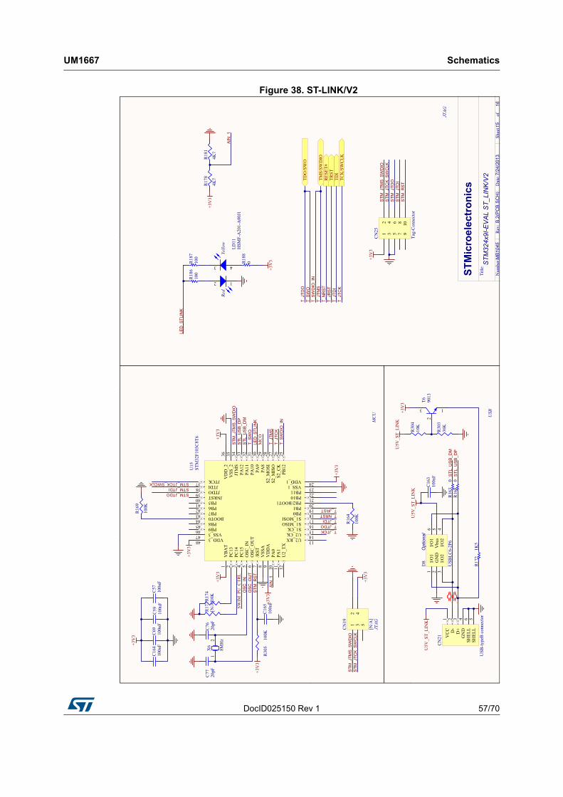
DocID025150 Rev 1 57/70
UM1667 Schematics
69
Figure 38. ST-LINK/V2
STMicroelec
tron
ics
Title:
Num
ber:
Rev:
Sheet of
B.2(PCB.SCH)
Date:7/24
/201
3MB10
4515
16
STM
324x
9I-EVAL ST_
LINK/V2
VBAT
1
PC13
2
PC14
3
PC15
4
OSC
_IN
5
OSC
_OUT
6
/RST
7
VSS
A8
VDDA
9
PA0
10
PA1
11
U2_
TX12
U2_RX 13
U2_CK 14
S1_CK 15
S1_MISO 16
S1_MOSI 17
PB0 18
PB1 19
PB2/BOOT1 20
PB10 21
VSS_1 23
VDD_1 24
PB12
25
PB11 22
S2_C
K26
S2_M
ISO
27S2
_MOSI
28PA
829
PA9
30PA
1031
PA11
32PA
1233
JTMS
34VSS
_235
VDD_2
36
JTCK37 JTDI38 JTDO39 JNRST40 PB541 PB642 PB743 BOOT044 PB845 PB946 VSS_347 VDD_348
U15
STM32F1
03C8T
6
20pF
C76
20pF
C77
12
X6
8MHz
+3V3
STL_
USB
_DM
STL_
USB
_DP
STM_R
ST
T_JTCK
T_JT
CK
T_JTDOT_JTDI
T_JT
MS
STM_J
TMS_
SWDIO
STM_JTCK_SWCLK
LED_S
TLINK
OSC
_IN
OSC
_OUT
T_NRSTT_JRST
LED_S
TLINK
T_JT
CK
T_JT
DI
T_JT
DO
T_NRST
T_JT
MS
T_JR
ST
R17
8
4K7
R18
1
4K7
AIN_1
C16
5100nF
R305
100K
+3V3
+3V3
+3V3
+3V3
+3V3
AIN_1
VCC
1
D-
2
D+
3
GND
4
SHEL
L6
SHEL
L5
CN21
USB
-typeB connector
STL_
USB
_DM
STL_
USB
_DP
+3V3 C
69100nF
C59
100nF
C57
100nF
C16
4100nF
MCU USB
JTAG
STM_J
TMS_
SWDIO
STM_J
TCK_
SWCLK
+3V3
U5V
_ST_
LINK
TDI
TRST
TMS/SW
DIO
TCK/SWCLK
TDO/SWO
RES
ET#
SWIM
_PU_C
TRL
R16
9
100K
T_SW
OT_
SWDIO
_IN
T_SW
DIO
_IN
T_SW
O
12
34
5
CN19
[N/A]
R30
410K
R30
336K
3
2
1
T6 9013
+3V3
U5V
_ST_
LINK
R17
7[N
/A]R17
410K
R16
4
100K
MCO
2 1
43
Red
Yello
w
LD11
HSM
F-A201-A00J1
+3V3
R18
6100
R18
7100
R18
80
C16
3100nF
I/O1
1
GND
2
I/O2
3I/O
24
Vbu
s5
I/O1
6D8
USB
LC6-2P
6
U5V
_ST_
LINK
R16
30
R16
80
R17
21K
5
+3V3
JTAG
12
34
56
78
910
CN25
Tag-Connector
+3V3
STM_J
TDO
STM_J
TDI
STM_J
TMS_
SWDIO
STM_J
TCK_
SWCLK
STM_JTDOSTM_JTDI
STM_R
ST
Optiona
l

Schematics UM1667
58/70 DocID025150 Rev 1
Figure 39. JTAG and trace
STMicroelec
tron
ics
Title:
Num
ber:
Rev:
Sheet of
B.2(PCB.SCH)
Date:7/24
/201
3MB10
4516
16
STM
324x
9I-EVAL JT
AG&Trac
e
1 2 3 4 5 6 7 8 9 10 11 12 13 14 15 16 17 18 19 20
CN13
P127B-2*10M
GF-079-1E
7A
R14
0[N
/A]
R14
2[N
/A]
R14
5[N
/A]R13
9[N
/A]
R14
4[N
/A]
1 2 3 4 5 6 7 8 9 10 11 12 13 14 15 16 17 18 19 20
CN16
JTAG
R14
810K
R14
910K
R14
310K
R11
3[N
/A]
R11
9[N
/A]
TDI
RES
ET#
TRACE_
D3
TRACE_
D2
TRACE_
D1
TRACE_
D0
TRACE_
CK
TRST
TMS/SW
DIO
TCK/SWCLK
TDO/SWO
Trac
e co
nnec
tor
JTAG con
nector
KEY
PA13
PA14
PB3
PA15
PB4
PE6
PE5
PE4
PE3
PE2
R13
6[N
/A]
D10 Z5V1
D11 Z5V1
D9 Z5V1
D14 Z5V1
D13 [N/A]
D12 Z5V1
+3V3
+3V3
+3V3
+3V3
R90
22R99
22R10
322
R10
622
R12
722
R10
922
FTSH-110
-01-L-DV (S
amtec)

DocID025150 Rev 1 59/70
UM1667 Schematics
69
Figure 40. 4.3' TFT LCD daughter board MB1046
STMicroelec
tron
ics
Title:
Num
ber:
Rev:
Sheet of
B.1(PCB.SCH)
Date:6/7/20
13MB10
461
1
4.3 inch
LCD boa
rd
Backlig
ht driv
er &
PFC
connector fo
r LCD panel
12
34
56
78
910
1112
1314
1516
1718
1920
2122
2324
2526
2728
2930
3132
3334
3536
3738
3940
4142
4344
4546
4748
4950
CN2
P127B-2*25M
GF-079-1A
VDD
R0
R1
R2
R3
R4
R5
R6
R7
B0
B1
B2
B3
B4
B5
B6
B7
G0
G1
G2
G3
G4
G5
G6
G7
I2C_S
DA
I2C_S
CL
ENB
HSY
NC
VSY
NC
INT
CLK
BL_
CTR
L
B1
B2
B3
B4
B5
B6
B7
B0
G0
G1
G2
G3
G4
G5
G6
G7
R0
R1
R2
R3
R4
R5
R6
R7
Y-
1
INT
2
A0/Data Out
3
SCLK
4
SDAT
5
VCC
6
Data in
7
IN0
8IN
19
GND
10
IN2
11IN
312
X+
13
Vio
14
Y+
15X-
16
U2
STMPE
811Q
TR
VDD
VDD
R14
[N/A]R15
[N/A]
VDD
C8
100nF
R20
100K
R17
100K
R18
100K
R22
100K
I2C_S
DA
I2C_S
CL
INT
XR
YD
YU
XL
XR
YD
YU
XL
HSY
NC
VSY
NC
CLK
ENB
R19
4K7
R5
4K7
R4
4K7
VDD
R7
[N/A]
R6
[N/A]
VDD
C1
4.7uF
C2
100nF
DCLK
38
HSY
NC
36
VSY
NC
37
ENB
52
U/D
46
NC
47
GND
48
NC
45
B0
12
B1
13
B2
14
B3
15
B4
16
B5
17
B6
18
B7
19
G0
20
G1
21
G2
22
G3
23
G4
24
G5
25
G6
26
G7
27
R0
28
R1
29
R2
30
R3
31
R4
32
R5
33
R6
34
R7
35GND
43
VCC
42VCC
41
NC
39
NC
40
DISP
6
VBL-
1
VBL-
2
VBL+
3
VBL+
4
R/L
44
YD
8
XR
9
YU
10
XL
11
GND
5
GND
49
GND
50
NC
51
GND
53
GND
54
GND
7
CN1
089H
54-000000-G2-C
A K
Z1 STPS
1L40M
C3
4.7uF/50V
L24.7u
H(1A)
R12
10
BLG
ND
BLV
DD
R11
100K
C7
4.7uF/10V
R10
0
R13 4K
7BLV
DD
BL_
CTR
L
BLG
ND
BLG
ND
BLG
ND
Vi
1
Rset
2GND
3FB
4
NC
5Vo
6
EN7
SW8
PGND
9
U1
STLD
40DPU
R
C6
10nF
C5
100nF
L1 BEA
D
C4
10nF
VLVH
BLG
ND
BLV
DD
R3
4K7
R2
4K7
R1
4K7
R8
4K7
R9
4K7
VDD
Connector fo
r motherboard
R21 [N
/A]
AM-480272H
3TMQW-T01H
TP1
TP2
TP3
TP4
TP5
GND
BLGND
VDD
VH VL
R16
4K7
Defau
lt I2C Add
ress:100
0001
R23
4K7
ON/OFF
ON/OFF
FTSH-125
-01-F-DV-K (S
amtec)
Note1: T
ext in italic placed on a wire
doesn’t correspond to net nam
e. It ju
st helps to
identify
rapidly MCU IO
related to th
is wire
.Note2: R
23 was added to
choose I2C address from Version A.1 to
B.1
Note3: R
9 was changed to
pull u
p from
Version A.1 to
B.1
H1
H2
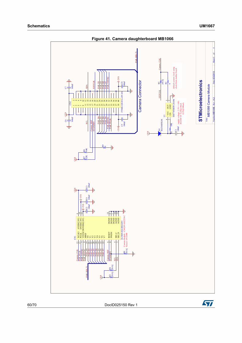
Schematics UM1667
60/70 DocID025150 Rev 1
Figure 41. Camera daughterboard MB1066
STMicroelec
tron
ics
Title:
Num
ber:
Rev:
Sheet of
A.2
Date:6/3/20
13MB10
661
1
MB10
66 Cam
era Mod
ule
+2V8
+2V8
C5
100nF
C8
100nF
C6
100nF
C7
100nF
+1V8
PAR_D
0PA
R_D
2PA
R_D
4PA
R_D
6
PAR_D
1PA
R_D
3PA
R_D
5PA
R_D
7
Cam
era Con
nector
EXTC
LK
SCL
12
34
56
78
910
1112
1314
1516
1718
1920
2122
2324
2526
2728
2930
3132
3334
3536
3738
3940
CN2
FTMH-120-03-L-DV-ES
Cam
era_RST
STANDBY
SDA
PAR_D
[0..7
]
PAR_H
SYNC
PAR_P
CLK
PAR_V
SYNC
EN1
GND
2OUT
3VCC
4U1
SM7745HEW
-24.0M
+2V8 R1
10K
R6
10K
R7
22K
+2V8
R5
[N/A]
R2
0
Cam
era_CLK
EXTC
LK
C3
100nF
C4
100nF
C2
100nF
R9
0
D1
BAT6
0JFILM
supply voltage: 2
.5V+/-10%
BAT6
0 VF: 0.28@
10mA
0.35@
100m
A
PAR_D
[0..7
]
+2V8
Cam
era_CLK
DGND
1DGND
2
SIO_D
3
AVDD(2.8V)
4
SIO_C
5
RES
ET6
VSY
NC
7
PWDN
8
HREF
9
DVDD(1.8V)
10
DOVDD(2.8V)
11
Y7
12
XCLK
113
Y6
14
DGND
15
Y5
16
PCLK
17
Y4
18
Y0
19
Y3
20
Y1
21
Y2
22
AGND
23AGND
24
CN1
24-5805-024-000-829+
+1V8
+2V8
R8
[N/A]
SCL
SDA
PAR_H
SYNC
PAR_V
SYNC
PAR_P
CLK
Cam
era_RST
PAR_D
0PA
R_D
1PA
R_D
2PA
R_D
3PA
R_D
4PA
R_D
5PA
R_D
6PA
R_D
7
Cam
era Module : C
N020V
AH2554-C
Sensor: O
V2640
STANDBY
default system clock using
clock from
mother b
oard.
C1
100nF
R4
[N/A]
R3
[N/A]
+2V8

DocID025150 Rev 1 61/70
UM1667 STM32429I-EVAL I/O assignment
69
Appendix A STM32429I-EVAL I/O assignment
Table 35. STM32429I-EVAL I/O assignment
Pin number Pin name STM32429I-EVAL standardMotor control variant
Camera variant
A1 PE4A20/ TRACED1
- -
A2 PE3A19/ TRACED0
- -
A3 PE2 TRACECLK - -
A4 PG14 MII_TXD1 - -
A5 PE1 NBL1 - -
A6 PE0 NBL0 - -
A7 PB8 MII_TXD3 DISSIPATIVE_BRAKE D6
A8 PB5 ULPI_D7 - -
A9 PB4 JTRST - -
A10 PB3JTDO-SWO/ I2S3_CK
- -
A11 PD7 NE1 - -
A12 PC12SDCARD_CK/ SPI3_MOSI
- D9
A13 PA15 JTDI - -
A14 PA14 JTCK-SWCLK - -
A15 PA13 JTMS-SWDIO - -
B1 PE5A21/ TRACED2
- -
B2 PE6A22/ SAI1_SD_A/ TRACED3
- D7
B3 PG13 MII_TXD0 - -
B4 PB9 I2C1_SDA - -
B5 PB7 - VSYNC
B6 PB6 I2C1_SCL - -
B7 PG15 SDNCAS - -
B8 PG11 MII_TX_EN NTC_BYPASS_IO -
B9 PJ13 LCD_B1 - -
B10 PJ12 LCD_B0 - -
B11 PD6NWAIT/ I2S3_SD
- D10

STM32429I-EVAL I/O assignment UM1667
62/70 DocID025150 Rev 1
B12 PD0 D2 - -
B13 PC11SDCARD_D3/ SPI3_MISO
- D4
B14 PC10SDCARD_D2/ SPI3_SCK
- D8
B15 PA12CAN1_TX/ USB_FS1_DP
PFC_SYNC2 -
C1 VBAT VBAT - -
C2PI8- ANTI TAMP2
EXPANDER_INT - -
C3 PI4 NBL2 - -
C4 PK7 LCD_DE - -
C5 PK6 LCD_B7 - -
C6 PK5 LCD_B6 - -
C7 PG12 LED4 - -
C8 PG10 LED3 - -
C9 PJ14 LCD_B2 - -
C10 PD5NWE - - -
C11 PD3 - - D5
C12 PD1 D3 - -
C13 PI3 D27 - -
C14 PI2 D26 - -
C15 PA11CAN1_RX/ USB_FS1_DM
PFC_PWM
D1 PC13 KEY_TAMP_1 - -
D2 PF0 A0 - -
D3 PI5 NBL3 - -
D4 PI7 D29 - -
D5 PI10D31/ MII_RX_ER
- -
D6 PI6 D28 - -
D7 PK4 LCD_B5 - -
D8 PK3 LCD_B4 - -
D9 PG9 NE2 - -
D10 PJ15 LCD_B3 - -
D11 PD4 NOE - -
Table 35. STM32429I-EVAL I/O assignment (continued)
Pin number Pin name STM32429I-EVAL standardMotor control variant
Camera variant

DocID025150 Rev 1 63/70
UM1667 STM32429I-EVAL I/O assignment
69
D12 PD2 SDCARD_CMD - D11
D13 PH15 D23 - -
D14 PI1 D25 - -
D15 PA10RS232_IRDA_RX/ USB_FS1_VBUS/ USB_FS1_ID
- -
E1 PC14 OSC32_IN - -
E2 PF1 A1 - -
E3 PI12 LCD_HSYNC - -
E4 PI9 D30 - -
E5 PDR_ON - - -
E6 BOOT0 BOOT0 - -
E7 VDD_3 - - -
E8 VDD_11 - - -
E9 VDD_10 - - -
E10 VDD_15 - - -
E11 VCAP2 - - -
E12 PH13 D21 - -
E13 PH14 D22 - -
E14 PI0 D24 - -
E15 PA9RS232/ IRDA_USART1_TX/ USB_FS1_VBUS
- -
F1 PC15 OSC32_OUT - -
F2 VSS_13_18 - - -
F3 PI11 ULPI_DIR
F4 VDD_13 - - -
F5 VDD_17 - - -
F6 VSS_3 - - -
F7 VSS_11 - - -
F8 VSS_10 - - -
F9 VSS_15 - - -
F10 VSS 2 - - -
F11 VDD_2 - - -
F12 PK1 LCD_G6 - -
Table 35. STM32429I-EVAL I/O assignment (continued)
Pin number Pin name STM32429I-EVAL standardMotor control variant
Camera variant

STM32429I-EVAL I/O assignment UM1667
64/70 DocID025150 Rev 1
F13 PK2 LCD_G7 - -
F14 PC9 SDCARD_D1 - D3
F15 PA8 LCD_BL_CTRL PFC_SYNC1 -
G1 PH0 OSC_IN - -
G2 PF2 A2 - -
G3 PI13 LCD_VSYNC - -
G4 PI15 LCD_R0 - -
G5 VDD_18 - - -
G6 VSS_17 - - -
G10 VSS_9 - - -
G11 VDD_9 - - -
G12 PJ11 LCD_G4 - -
G13 PK0 LCD_G5 - -
G14 PC8 SDCARD_D0 WH D2
G15 PC7 - VH D1
H1 PH1 OSC_OUT - -
H2 PF3 A3 - -
H3 PI14 LCD_CLK - -
H4 PH4 ULPI_NXT - -
H5 VDD_5 - - -
H6 VSS_5 - - -
H10 VSS_20 - - -
H11 VDD_20 - - -
H12 PJ8 LCD_G1 - -
H13 PJ10 LCD_G3 - -
H14 PG8SDCLK/ MII_PPS_OUT
- -
H15 PC6 LCD_ON_OFF UH D0
J1 NRST NRST - -
J2 PF4 A4 - -
J3 PH5 SDNWE - -
J4 PH3SDNE0/ MII_COL
- -
J5 VDD_12 - - -
J6 VSS_12 - - -
Table 35. STM32429I-EVAL I/O assignment (continued)
Pin number Pin name STM32429I-EVAL standardMotor control variant
Camera variant

DocID025150 Rev 1 65/70
UM1667 STM32429I-EVAL I/O assignment
69
J10 VSS_8 - - -
J11 VDD_8 - - -
J12 PJ7 LCD_G0 - -
J13 PJ9 LCD_G2 - -
J14 PG7 LED2 - -
J15 PG6 LED1 - -
K1 PF7 SAI1_MCLK_B - -
K2 PF6 SAI1_SD_B - -
K3 PF5 A5 - -
K4 PH2 SDCKE0 - -
K5 VDD_4 - - -
K6 VSS_4 - - -
K7 VSS_6 - - -
K8 VSS_7 - - -
K9 VSS_1 - - -
K10 VSS_14 - - -
K11 VDD_14 - - -
K12 PJ6 LCD_R7
K13 PD15 D1 - -
K14 PB13ULPI_D6/ USB_FS2_VBUS
- -
K15 PD10 D15 - -
L1 PF10 Potentiometer - -
L2 PF9 SAI1_FS_B - -
L3 PF8 SAI1_SCK_B - -
L4 PC3 MII_TX_CLK CURRENT_C -
L5BYPASS_REG
- - -
L6 VSS_19 - - -
L7 VDD_19 - - -
L8 VDD_6 - - -
L9 VDD_7 - - -
L10 VDD_1 - - -
L11 VCAP1 - - -
L12 PD14 D0 - -
Table 35. STM32429I-EVAL I/O assignment (continued)
Pin number Pin name STM32429I-EVAL standardMotor control variant
Camera variant

STM32429I-EVAL I/O assignment UM1667
66/70 DocID025150 Rev 1
L13 PB12ULPI_D5/ USB_FS2_ID
- -
L14 PD9 D14 - -
L15 PD8 D13 - -
M1 VSSA - - -
M2 PC0 ULPI_STP - -
M3 PC1 MII_MDC - -
M4 PC2 MII_TXD2 CURRENT_B -
M5 PB2 BOOT1 - -
M6 PF12 A6 - -
M7 PG1 A11 - -
M8 PF15 A9 - -
M9 PJ4 LCD_R5 - -
M10 PD12 A17 - -
M11 PD13 A18 - -
M12 PG3 A13 - -
M13 PG2 A12 - -
M14 PJ5 LCD_R6 - -
M15 PH12 D20 - -
N1 VREF- - - -
N2 PA1 MII_RX_CLK ENCODER_B -
N3 PA0KEY_WKUP/ MII_CRS
ENCODER_A -
N4 PA4 - DAC_OUT1 HSYNC
N5 PC4 MII_RXD0 BUSVOLTAGE -
N6 PF13 A7 - -
N7 PG0 A10 - -
N8 PJ3 LCD_R4 - -
N9 PE8 D5 - -
N10 PD11 A16 - -
N11 PG5A15/ BA1
- -
N12 PG4A14/ BA0
- -
N13 PH7 MII_RXD3 - -
Table 35. STM32429I-EVAL I/O assignment (continued)
Pin number Pin name STM32429I-EVAL standardMotor control variant
Camera variant

DocID025150 Rev 1 67/70
UM1667 STM32429I-EVAL I/O assignment
69
N14 PH9 D17 - -
N15 PH11 D19 - -
P1 VREF+ - - -
P2 PA2 MII_MDIO INDEX -
P3 PA6 - STOP PIXCK
P4 PA5 ULPI_CK DAC_OUT2 -
P5 PC5 MII_RXD1 HEATSINK -
P6 PF14 A8 - -
P7 PJ2 LCD_R3 - -
P8 PF11 SDNRAS - -
P9 PE9 D6 - -
P10 PE11 D8 - -
P11 PE14 D11 - -
P12 PB10 ULPI_D3 - -
P13 PH6 MII_RXD2 - -
P14 PH8 D16 - -
P15 PH10 D18 - -
R1 VDDA - - -
R2 PA3 ULPI_D0 - -
R3 PA7 MII_RX_DV UL -
R4 PB1 ULPI_D2 WL -
R5 PB0 ULPI_D1 VL -
R6 PJ0 LCD_R1 - -
R7 PJ1 LCD_R2 - -
R8 PE7 D4 - -
R9 PE10 D7 - -
R10 PE12 D9 - -
R11 PE15 D12 - -
R12 PE13 D10 - -
R13 PB11 ULPI_D4 - -
R14 PB14 USB_FS2_DM - -
R15 PB15 USB_FS2_DP - -
Table 35. STM32429I-EVAL I/O assignment (continued)
Pin number Pin name STM32429I-EVAL standardMotor control variant
Camera variant

Mechanical dimensions UM1667
68/70 DocID025150 Rev 1
Appendix B Mechanical dimensions
Figure 42. Mechanical dimensions
Table 36. Mechanical dimensions
Symbol Size (mm) Symbol Size (mm) Symbol Size (mm)
A1 68.58 E3 114.18 Mx 20.1
A2 48.62 E4 122 My 24.43
a 1.27 e 116.5 P1 16.94
D 4.5 H 25 P2 55.37
d 3.5 Lx1 21.36 Q1 46.77
E1 55 Lx2 32.64 Q2 9.98
E2 68 Ly1 5 X 157
Ly2 6.4 Y 172.72

DocID025150 Rev 1 69/70
UM1667 Revision history
69
Revision history
Table 37. Document revision history
Date Revision Changes
12-Sept-2013 1 Initial release
06-Mar-2015 2Updated document title, Table 7: USB OTG2 configuration, Figure 24: STM32429I-EVAL

UM1667
70/70 DocID025150 Rev 1
IMPORTANT NOTICE – PLEASE READ CAREFULLY
STMicroelectronics NV and its subsidiaries (“ST”) reserve the right to make changes, corrections, enhancements, modifications, and improvements to ST products and/or to this document at any time without notice. Purchasers should obtain the latest relevant information on ST products before placing orders. ST products are sold pursuant to ST’s terms and conditions of sale in place at the time of order acknowledgement.
Purchasers are solely responsible for the choice, selection, and use of ST products and ST assumes no liability for application assistance or the design of Purchasers’ products.
No license, express or implied, to any intellectual property right is granted by ST herein.
Resale of ST products with provisions different from the information set forth herein shall void any warranty granted by ST for such product.
ST and the ST logo are trademarks of ST. All other product or service names are the property of their respective owners.
Information in this document supersedes and replaces information previously supplied in any prior versions of this document.
© 2015 STMicroelectronics – All rights reserved


![Datasheet - MP34DT06J - st.com · Order code MP34DT06JTR Temperature range [°C]-40 °C to +85 Package HCLGA (3 x 4 x 1 mm) 4 LD Packing Tape and reel MEMS audio sensor omnidirectional](https://img.pdfslide.us/doc/110x75/5e17fc36157f454a4d267ec4/datasheet-mp34dt06j-stcom-order-code-mp34dt06jtr-temperature-range-c-40.jpg)