Embed Size (px)
Citation preview
LLC Resonant Half Bridge Converter
Asia Tech-Day
August 17 to 27, 2009
Hong HuangApplications Engineer
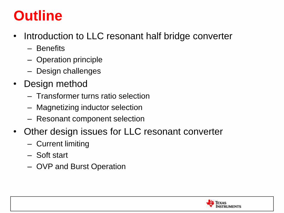
Outline
• Introduction to LLC resonant half bridge converter
– Benefits
– Operation principle
– Design challenges
• Design method
– Transformer turns ratio selection
– Magnetizing inductor selection
– Resonant component selection
• Other design issues for LLC resonant converter
– Current limiting
– Soft start
– OVP and Burst Operation
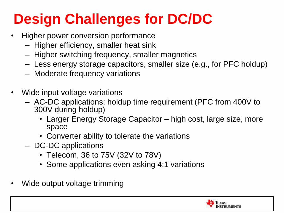
Design Challenges for DC/DC• Higher power conversion performance
– Higher efficiency, smaller heat sink
– Higher switching frequency, smaller magnetics
– Less energy storage capacitors, smaller size (e.g., for PFC holdup)
– Moderate frequency variations
• Wide input voltage variations
– AC-DC applications: holdup time requirement (PFC from 400V to 300V during holdup)
• Larger Energy Storage Capacitor – high cost, large size, more space
• Converter ability to tolerate the variations
– DC-DC applications
• Telecom, 36 to 75V (32V to 78V)
• Some applications even asking 4:1 variations
• Wide output voltage trimming
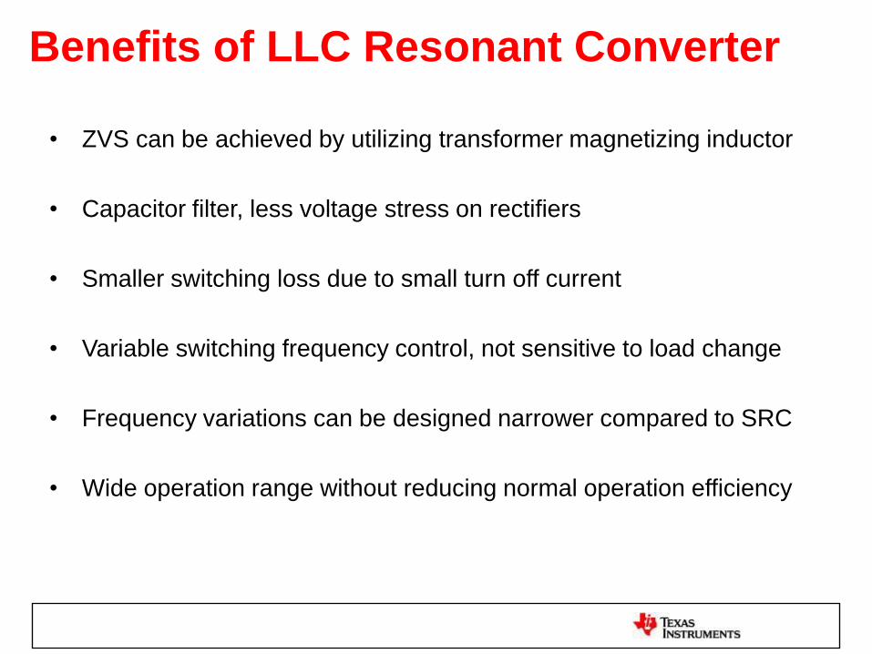
Benefits of LLC Resonant Converter
• ZVS can be achieved by utilizing transformer magnetizing inductor
• Capacitor filter, less voltage stress on rectifiers
• Smaller switching loss due to small turn off current
• Variable switching frequency control, not sensitive to load change
• Frequency variations can be designed narrower compared to SRC
• Wide operation range without reducing normal operation efficiency
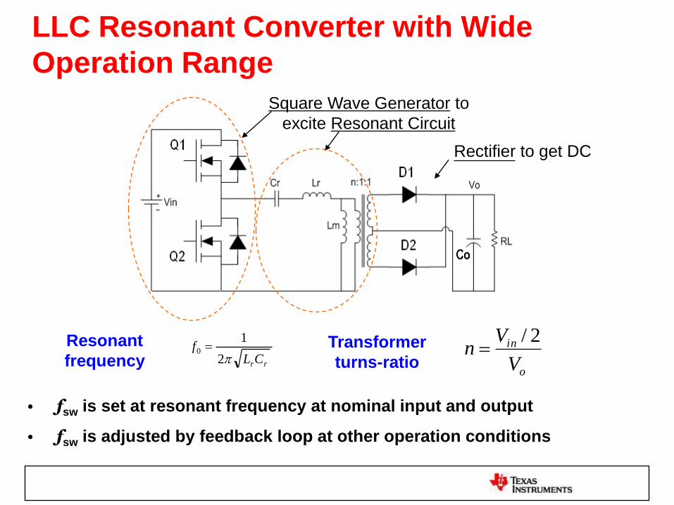
LLC Resonant Converter with Wide
Operation Range
• fsw is set at resonant frequency at nominal input and output
• fsw is adjusted by feedback loop at other operation conditions
o
in
V
Vn
2/Transformer
turns-ratiorrCLf
2
10
Resonant
frequency
Square Wave Generator to
excite Resonant Circuit
Rectifier to get DC
Cr Lr
Lm
n:1:1
Vin
Vo
RL
Q1
Q2
D1
D2
*
*
*
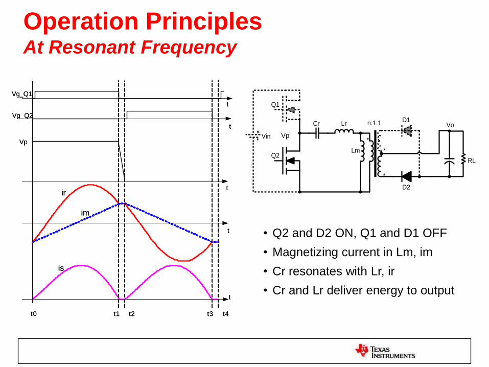
Operation PrinciplesAt Resonant Frequency
Vp
• Q2 and D2 ON, Q1 and D1 OFF
• Magnetizing current in Lm, im
• Cr resonates with Lr, ir
• Cr and Lr deliver energy to output
Vg_Q1
Vg_Q2
Vp
ir
im
is
t
t
t
t
t
t0 t1 t2 t3 t4
Vg_Q1
Vg_Q2
Vp
ir
im
is
t
t
t
t
t
t0 t1 t2 t3 t4
Cr Lr
Lm
n:1:1
Vin
Vo
RL
Q1
Q2
D1
D2
*
*
*
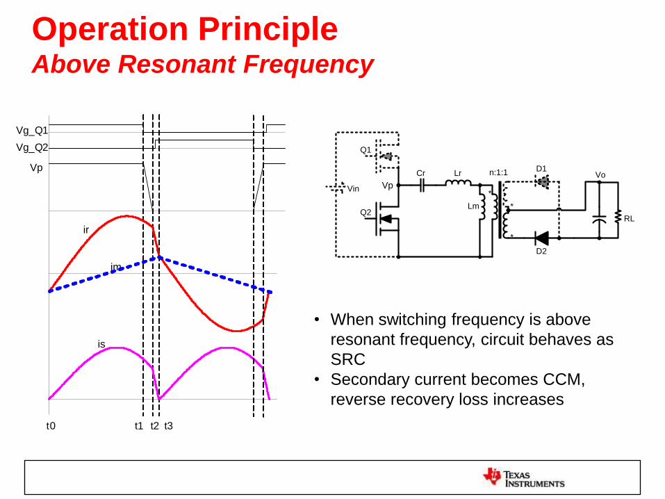
Operation PrincipleAbove Resonant Frequency
• When switching frequency is above
resonant frequency, circuit behaves as
SRC
• Secondary current becomes CCM,
reverse recovery loss increases
Vp
t0 t1 t2 t3
Vg_Q1
Vg_Q2
Vp
ir
im
is
Cr Lr
Lm
n:1:1
Vin
Vo
RL
Q1
Q2
D1
D2
*
*
*
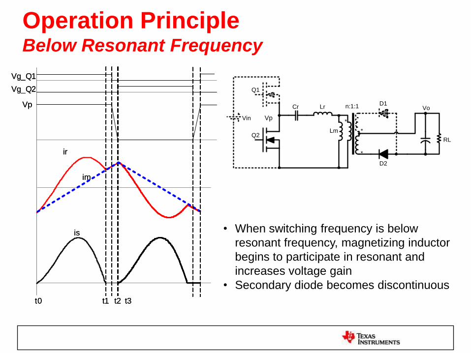
Operation PrincipleBelow Resonant Frequency
• When switching frequency is below
resonant frequency, magnetizing inductor
begins to participate in resonant and
increases voltage gain
• Secondary diode becomes discontinuous
Vp
t0 t1 t2 t3
Vg_Q1
Vg_Q2
Vp
ir
im
is
t0 t1 t2 t3
Vg_Q1
Vg_Q2
Vp
ir
im
is
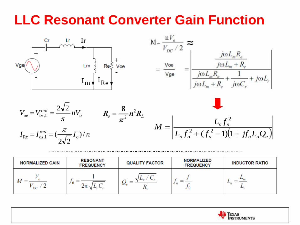
LLC Resonant Converter Gain Function
ennnnn
nn
QLjfffL
fLM
1)1( 22
2o
rmsosoe nVVV
221,
nIII ormsos /)
22(1,Re
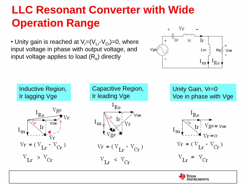
LLC Resonant Converter with Wide
Operation Range
• Unity gain is reached at Vr=(VLr-VCr)=0, where
input voltage in phase with output voltage, and
input voltage applies to load (Re) directly
Inductive Region,
Ir lagging Vge
Capacitive Region,
Ir leading VgeUnity Gain, Vr=0
Voe in phase with Vge
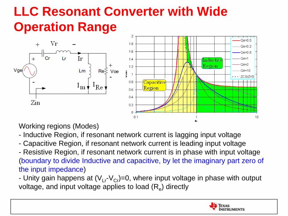
LLC Resonant Converter with Wide
Operation Range
Working regions (Modes)
- Inductive Region, if resonant network current is lagging input voltage
- Capacitive Region, if resonant network current is leading input voltage
- Resistive Region, if resonant network current is in phase with input voltage
(boundary to divide Inductive and capacitive, by let the imaginary part zero of
the input impedance)
- Unity gain happens at (VLr-VCr)=0, where input voltage in phase with output
voltage, and input voltage applies to load (Re) directly
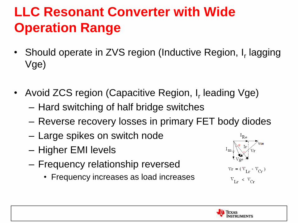
LLC Resonant Converter with Wide
Operation Range
• Should operate in ZVS region (Inductive Region, Ir lagging
Vge)
• Avoid ZCS region (Capacitive Region, Ir leading Vge)
– Hard switching of half bridge switches
– Reverse recovery losses in primary FET body diodes
– Large spikes on switch node
– Higher EMI levels
– Frequency relationship reversed
• Frequency increases as load increases
0
0.2
0.4
0.6
0.8
1
1.2
1.4
1.6
1.8
2
0.1 1 10fn, (Ln =1)
Ga
in
Qe=0.0
Qe=0.2
Qe=0.8
Qe=1
Qe=2
Qe=10
ZCS/ZVS
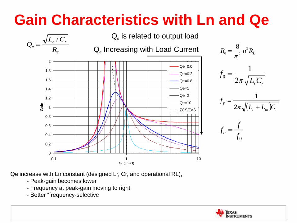
Gain Characteristics with Ln and Qe
rmr
p
CLLf
2
1
0f
ffn
Le RnR 2
2
8
e
rr
eR
CLQ
/
Qe is related to output load
Qe Increasing with Load Current
rrCLf
2
10
Qe increase with Ln constant (designed Lr, Cr, and operational RL),
- Peak-gain becomes lower
- Frequency at peak-gain moving to right
- Better “frequency-selective
0
0.2
0.4
0.6
0.8
1
1.2
1.4
1.6
1.8
2
0.1 1 10
fn, (Ln =1)
Ga
in
Qe=0.1
Qe=0.2
Qe=0.5
Qe=0.8
Qe=1
Qe=2
Qe=5
Qe=8
Qe=10
ZCS/ZVS
0
0.2
0.4
0.6
0.8
1
1.2
1.4
1.6
1.8
2
0.1 1 10
fn, (Ln =5)
Ga
in
Qe=0.1
Qe=0.2
Qe=0.5
Qe=0.8
Qe=1
Qe=2
Qe=5
Qe=8
Qe=10
ZCS/ZVS
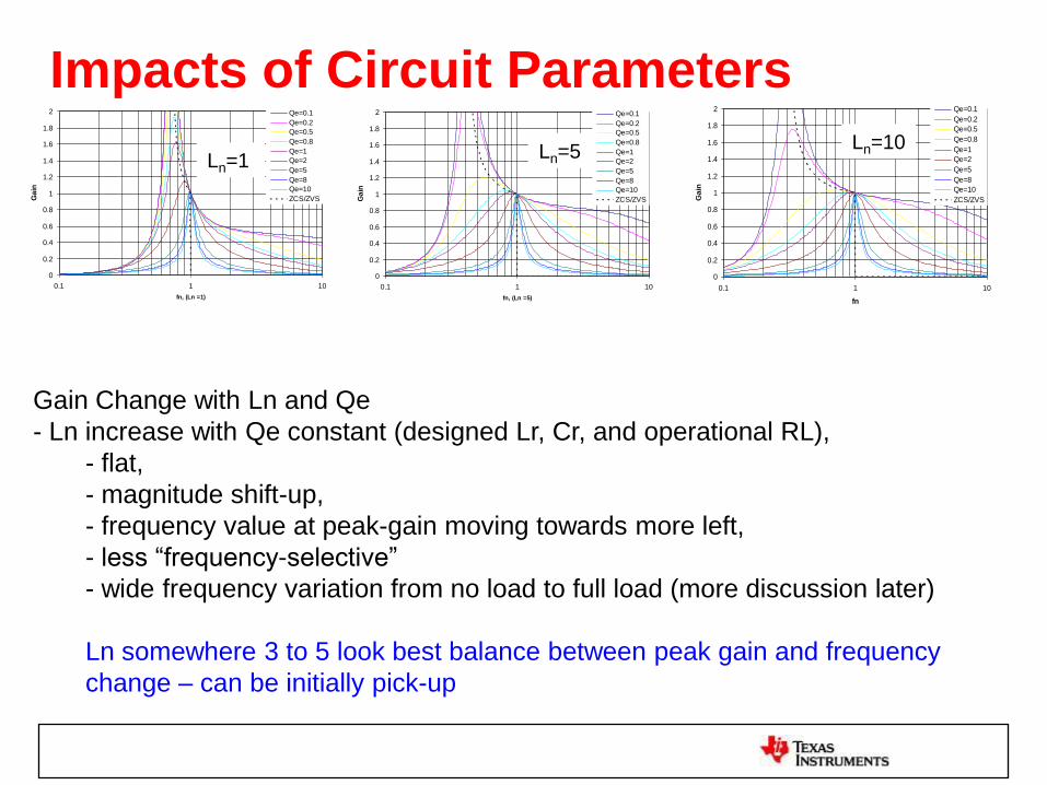
Impacts of Circuit Parameters
0
0.2
0.4
0.6
0.8
1
1.2
1.4
1.6
1.8
2
0.1 1 10
fn
Ga
in
Qe=0.1
Qe=0.2
Qe=0.5
Qe=0.8
Qe=1
Qe=2
Qe=5
Qe=8
Qe=10
ZCS/ZVS
Ln=1Ln=10Ln=5
Gain Change with Ln and Qe
- Ln increase with Qe constant (designed Lr, Cr, and operational RL),
- flat,
- magnitude shift-up,
- frequency value at peak-gain moving towards more left,
- less “frequency-selective”
- wide frequency variation from no load to full load (more discussion later)
Ln somewhere 3 to 5 look best balance between peak gain and frequency
change – can be initially pick-up
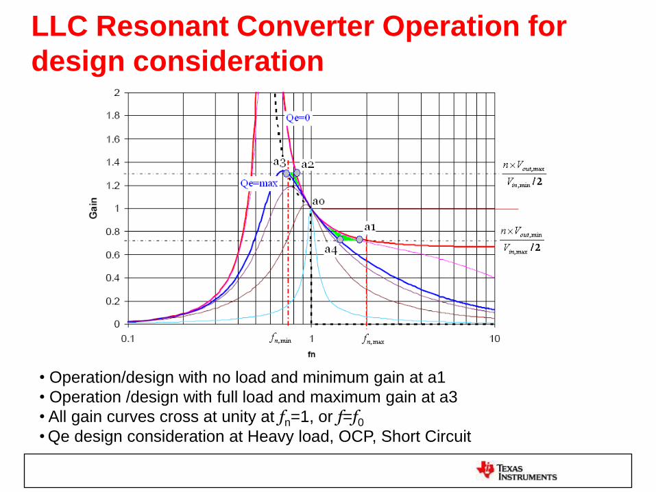
LLC Resonant Converter Operation for
design consideration
• Operation/design with no load and minimum gain at a1
• Operation /design with full load and maximum gain at a3
• All gain curves cross at unity at fn=1, or f=f0• Qe design consideration at Heavy load, OCP, Short Circuit
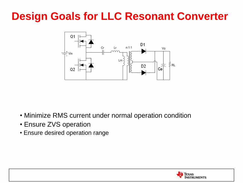
Design Goals for LLC Resonant Converter
• Minimize RMS current under normal operation condition
• Ensure ZVS operation
• Ensure desired operation range
22
2Re
2,
22
22
n
I
L
nVFHA
IIII
o
m
O
mrRMSP
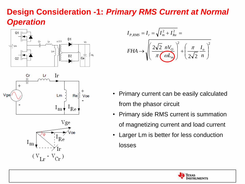
Design Consideration -1: Primary RMS Current at Normal
Operation
• Primary current can be easily calculated
from the phasor circuit
• Primary side RMS current is summation
of magnetizing current and load current
• Larger Lm is better for less conduction
losses
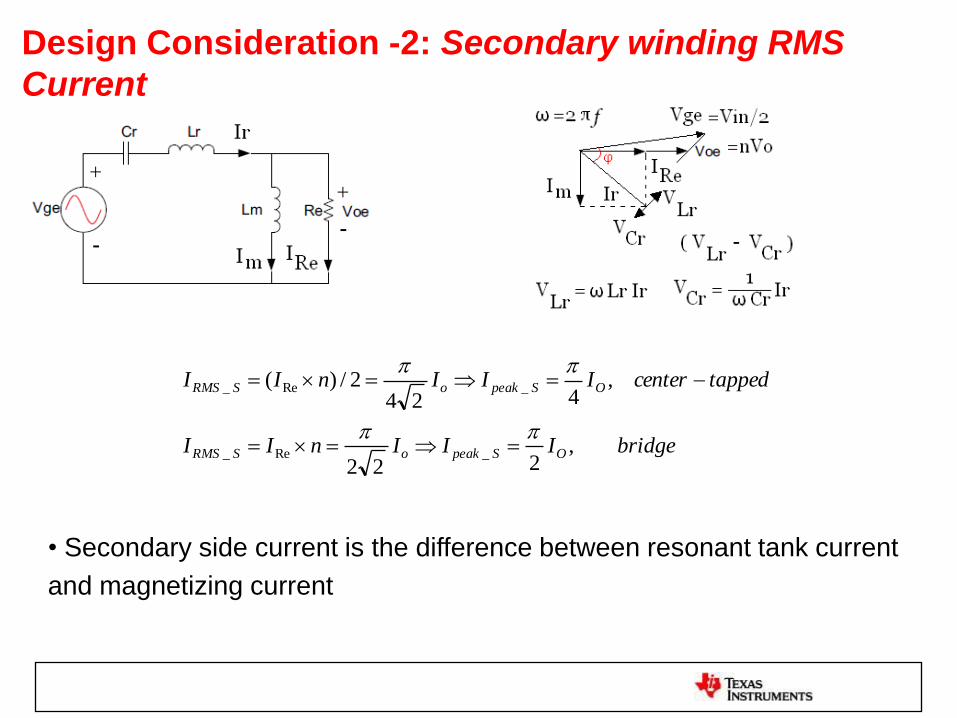
Design Consideration -2: Secondary winding RMS
Current
• Secondary side current is the difference between resonant tank current
and magnetizing current
bridgeIIInII
tappedcenterIIInII
OSpeakoSRMS
OSpeakoSRMS
,222
,424
2/)(
_Re_
_Re_
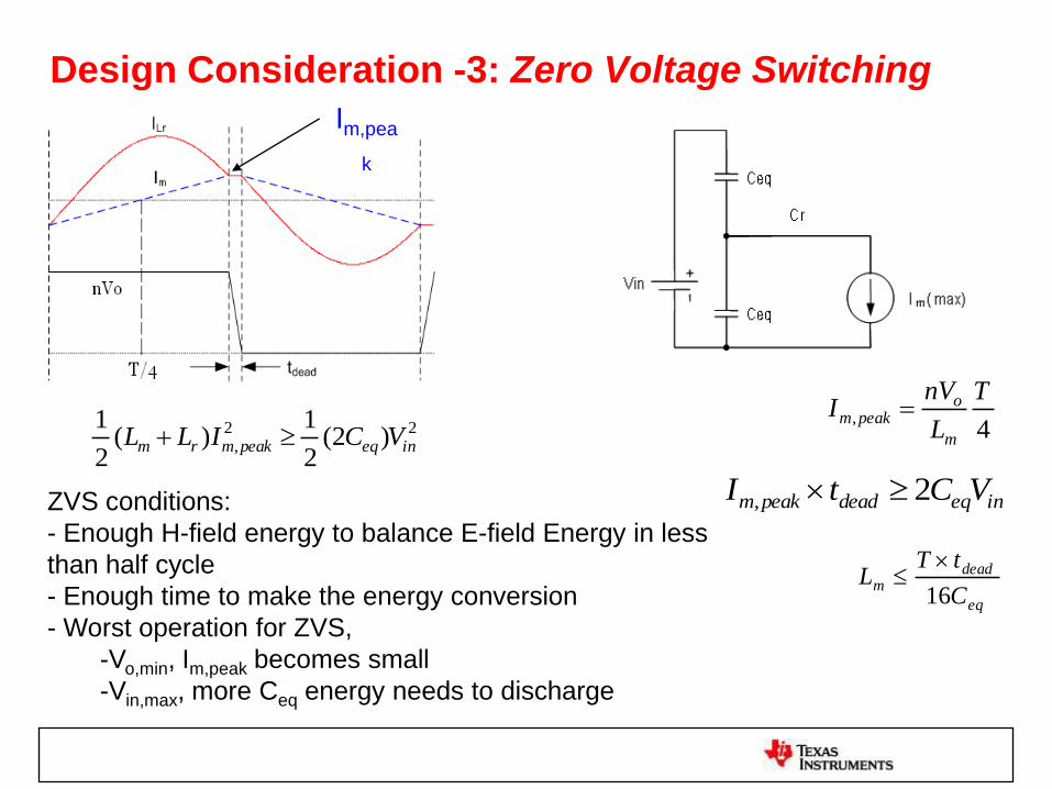
Design Consideration -3: Zero Voltage Switching
4,
T
L
nVI
m
opeakm
Im,pea
k
ineqdeadpeakm VCtI 2,
22, )2(
2
1)(
2
1ineqpeakmrm VCILL
ZVS conditions:
- Enough H-field energy to balance E-field Energy in less
than half cycle
- Enough time to make the energy conversion
- Worst operation for ZVS,
-Vo,min, Im,peak becomes small
-Vin,max, more Ceq energy needs to discharge
eq
deadm
C
tTL
16
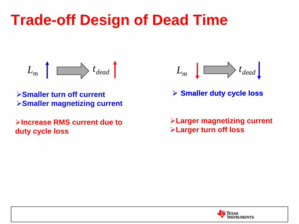
Trade-off Design of Dead Time
mL
Smaller turn off current
Smaller magnetizing current
deadt
Increase RMS current due to
duty cycle loss
Larger magnetizing current
Larger turn off loss
Smaller duty cycle loss Smaller duty cycle loss
mL deadt
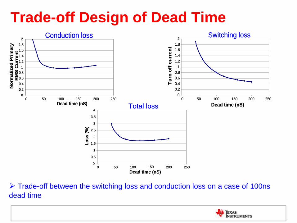
Trade-off Design of Dead Time
Trade-off between the switching loss and conduction loss on a case of 100ns
dead time
0
0.2
0.4
0.6
0.8
1
1.2
1.4
1.6
1.8
2
0 50 100 150 200 250
Dead time (nS)
Tu
rn o
ff c
urr
en
t
Switching loss
0
0.2
0.4
0.6
0.8
1
1.2
1.4
1.6
1.8
2
0 50 100 150 200 250
Dead time (nS)
Tu
rn o
ff c
urr
en
t
Switching loss
0
0.2
0.4
0.6
0.8
1
1.2
1.4
1.6
1.8
2
0 50 100 150 200 250
Dead time (nS)
No
rma
lize
d P
rim
ary
RM
S C
urr
en
t
Conduction loss
0
0.2
0.4
0.6
0.8
1
1.2
1.4
1.6
1.8
2
0 50 100 150 200 250
Dead time (nS)
No
rma
lize
d P
rim
ary
RM
S C
urr
en
t
Conduction loss
0
0.5
1
1.5
2
2.5
3
3.5
4
0 50 100 150 200 250
Dead time (nS)
Lo
ss
(%
)
Total loss
0
0.5
1
1.5
2
2.5
3
3.5
4
0 50 100 150 200 250
Dead time (nS)
Lo
ss
(%
)
Total loss
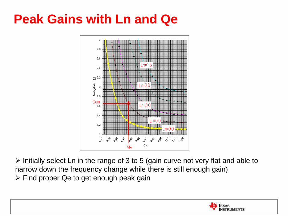
Peak Gains with Ln and Qe
Initially select Ln in the range of 3 to 5 (gain curve not very flat and able to
narrow down the frequency change while there is still enough gain)
Find proper Qe to get enough peak gain
Design Flow Chart for LLC Resonant Converter
out
oLe
P
VnRnR
2
222
2
88
Converter Specifications
choose an Ln and Qe
O
in
V
Vn
2
Check max gain
against graph
Peak gain enough?Yes
Calculate Re
No
Change Ln and Qe
Resonant Capacitor
rnm LLL
Resonant Inductor
rsw
rCf
L2
2
1
swee
rfRQ
C2
1
Magnetizing Inductance
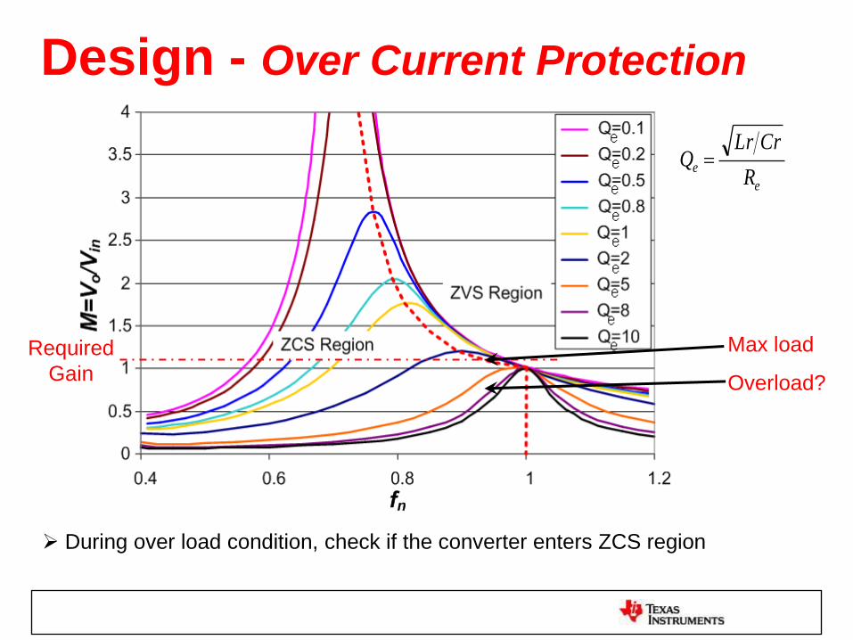
Design - Over Current Protection
During over load condition, check if the converter enters ZCS region
e
eR
CrLrQ
Max load
Overload?
Required
Gain
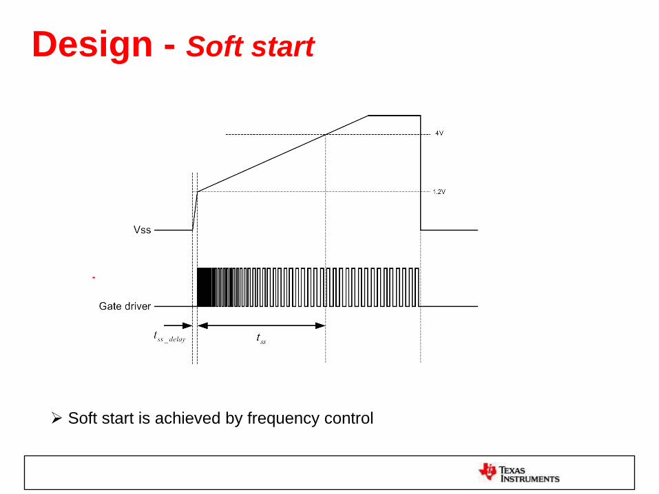
Design - Soft start
Soft start is achieved by frequency control
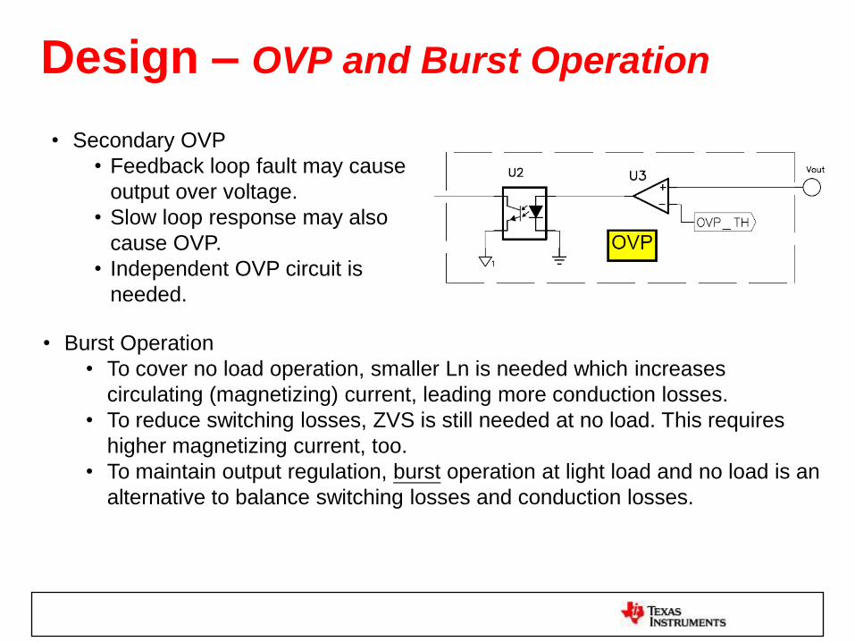
Design – OVP and Burst Operation
• Burst Operation
• To cover no load operation, smaller Ln is needed which increases
circulating (magnetizing) current, leading more conduction losses.
• To reduce switching losses, ZVS is still needed at no load. This requires
higher magnetizing current, too.
• To maintain output regulation, burst operation at light load and no load is an
alternative to balance switching losses and conduction losses.
• Secondary OVP
• Feedback loop fault may cause
output over voltage.
• Slow loop response may also
cause OVP.
• Independent OVP circuit is
needed.
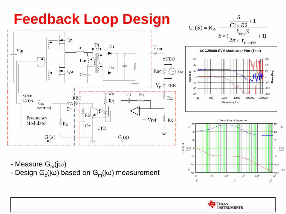
Feedback Loop Design
- Measure Gm(jω)
- Design Gc(jω) based on Gm(jω) measurement10 100 1 10
31 10
41 10
51 10
660
40
20
0
20
40
60
180
120
60
0
60
120
180
Gain of Type I Compensator
Gain
(d
B)
60
60
Gc f( )
180
180
c f( )
10610 f
)12
(
121)(
_
optop
optodcc
f
SkS
RC
S
KSG
UCC25600 EVM Modulator Plot (Test)
-60
-40
-20
0
20
40
60
10 100 1000 10000 100000 1000000
Frequency (Hz)
Gain
(d
B)
-180
-120
-60
0
60
120
180
Ph
ase (
Deg
)
Summary
• Due to low switching losses, LLC resonant converter is
able to operate at high switching frequencies, while
maintaining high efficiency
• LLC resonant converter design needs to find a suitable
magnetizing inductor to ensure small conduction losses
and switching losses
• LLC resonant converter is able to achieve wide
operation together with high efficiency
• By choosing a suitable Ln and Qe value, desired voltage
gain can be achieved to input and output voltage variation
range
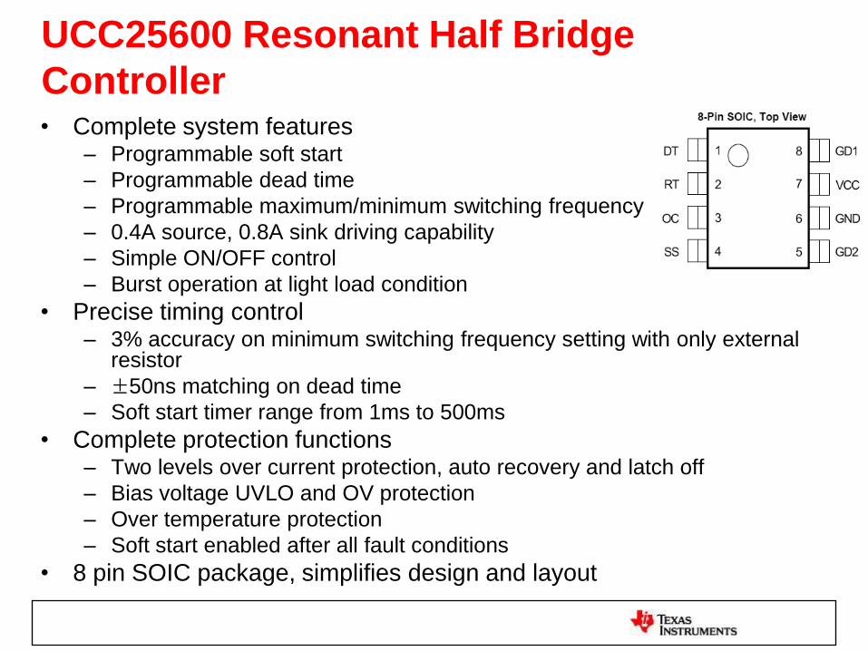
• Complete system features– Programmable soft start
– Programmable dead time
– Programmable maximum/minimum switching frequency
– 0.4A source, 0.8A sink driving capability
– Simple ON/OFF control
– Burst operation at light load condition
• Precise timing control– 3% accuracy on minimum switching frequency setting with only external
resistor
– ±50ns matching on dead time
– Soft start timer range from 1ms to 500ms
• Complete protection functions– Two levels over current protection, auto recovery and latch off
– Bias voltage UVLO and OV protection
– Over temperature protection
– Soft start enabled after all fault conditions
• 8 pin SOIC package, simplifies design and layout
UCC25600 Resonant Half Bridge
Controller
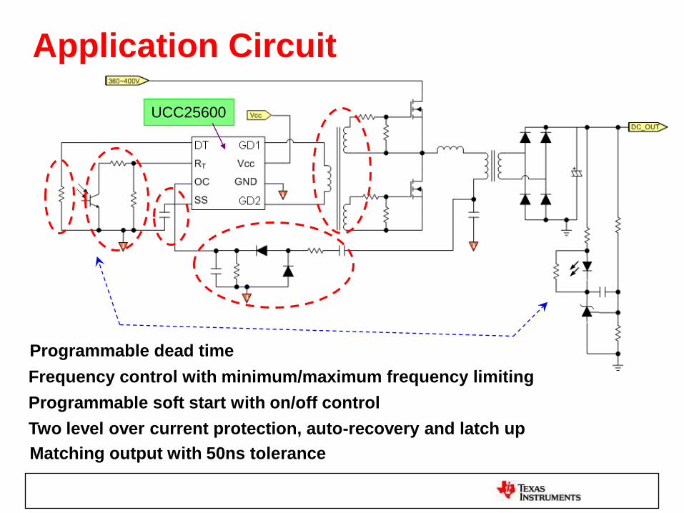
Programmable dead time
Frequency control with minimum/maximum frequency limiting
Programmable soft start with on/off control
Two level over current protection, auto-recovery and latch up
Matching output with 50ns tolerance
Application Circuit
UCC25600
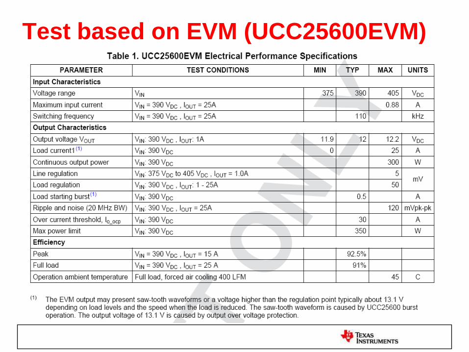
Test based on EVM (UCC25600EVM)
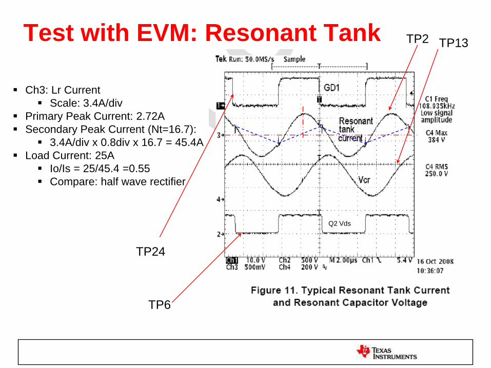
Test with EVM: Resonant Tank
Q2 Vds
Ch3: Lr Current
Scale: 3.4A/div
Primary Peak Current: 2.72A
Secondary Peak Current (Nt=16.7):
3.4A/div x 0.8div x 16.7 = 45.4A
Load Current: 25A
Io/Is = 25/45.4 =0.55
Compare: half wave rectifier
TP2 TP13
TP6
TP24
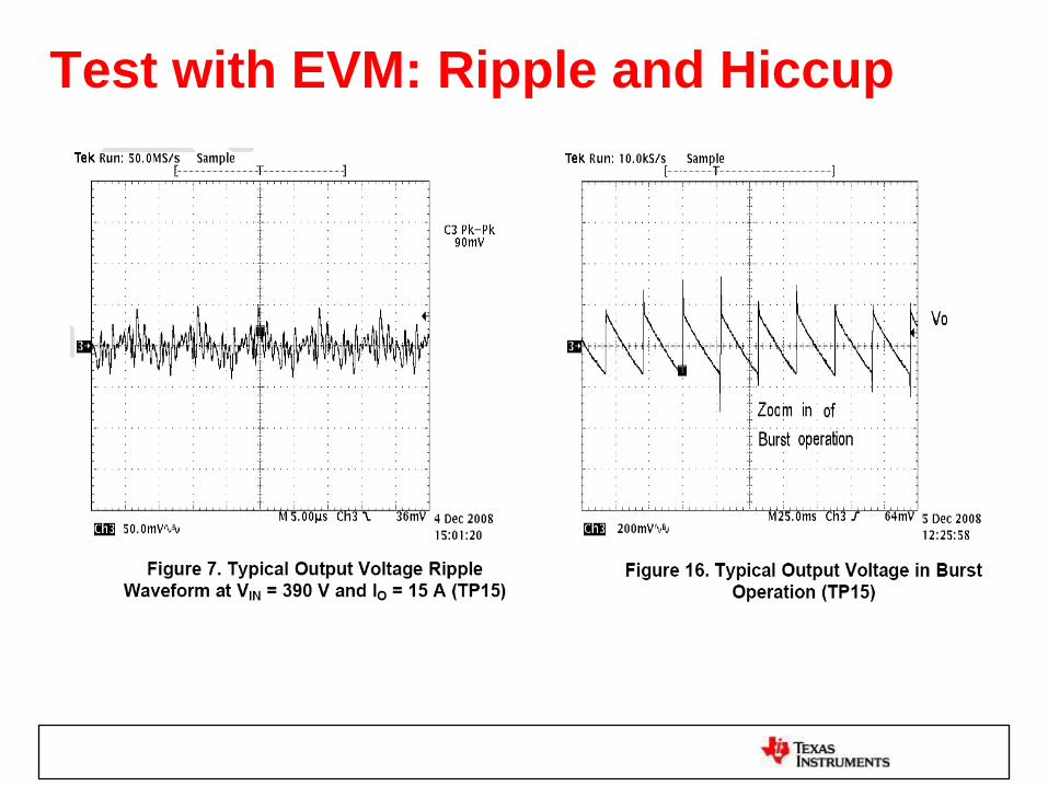
Test with EVM: Ripple and Hiccup
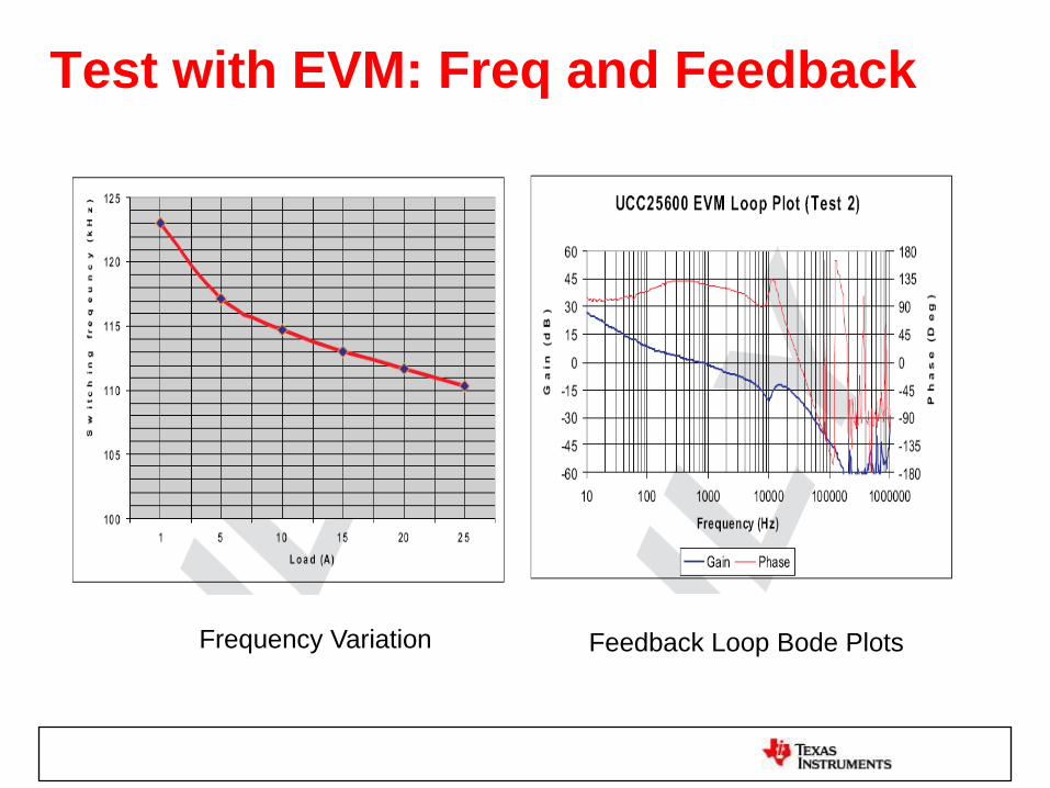
Test with EVM: Freq and Feedback
Frequency Variation Feedback Loop Bode Plots
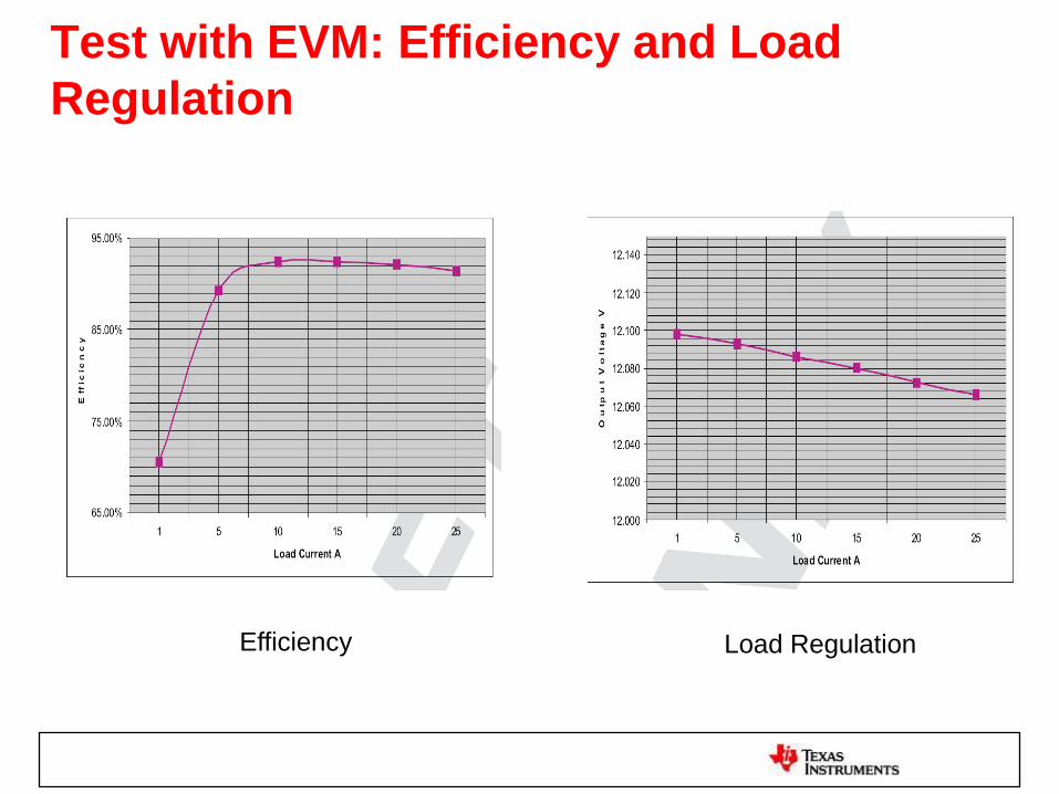
Test with EVM: Efficiency and Load
Regulation
Efficiency Load Regulation

Thank You!