Embed Size (px)
Citation preview
MODELLING AND CONTROL OF THE LLC RESONANT CONVERTER
by
Brian Cheak Shing Cheng
B.Sc., Queen's University, 2010
A THESIS SUBMITTED IN PARTIAL FULFILLMENT OF
THE REQUIREMENT FOR THE DEGREE OF
MASTER OF APPLIED SCIENCE
in
The Faculty of Graduate Studies
(Electrical & Computer Engineering)
THE UNIVERSITY OF BRITISH COLUMBIA
(Vancouver)
December 2012
c© Brian Cheak Shing Cheng, 2012
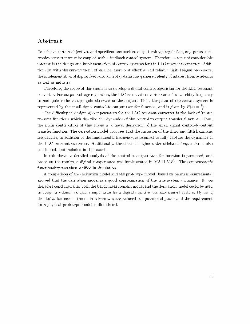
Abstract
To achieve certain objectives and speci�cations such as output voltage regulation, any power elec-
tronics converter must be coupled with a feedback control system. Therefore, a topic of considerable
interest is the design and implementation of control systems for the LLC resonant converter. Addi-
tionally, with the current trend of smaller, more cost e�ective and reliable digital signal processors,
the implementation of digital feedback control systems has garnered plenty of interest from academia
as well as industry.
Therefore, the scope of this thesis is to develop a digital control algorithm for the LLC resonant
converter. For output voltage regulation, the LLC resonant converter varies its switching frequency
to manipulate the voltage gain observed at the output. Thus, the plant of the control system is
represented by the small signal control-to-output transfer function, and is given by P (s) = Vo
f .
The di�culty in designing compensators for the LLC resonant converter is the lack of known
transfer functions which describe the dynamics of the control-to-output transfer function. Thus,
the main contribution of this thesis is a novel derivation of the small signal control-to-output
transfer function. The derivation model proposes that the inclusion of the third and �fth harmonic
frequencies, in addition to the fundamental frequency, is required to fully capture the dynamics of
the LLC resonant converter. Additionally, the e�ect of higher order sideband frequencies is also
considered, and included in the model.
In this thesis, a detailed analysis of the control-to-output transfer function is presented, and
based on the results, a digital compensator was implemented in MATLAB R©. The compensator's
functionality was then veri�ed in simulation.
A comparison of the derivation model and the prototype model (based on bench measurements)
showed that the derivation model is a good approximation of the true system dynamics. It was
therefore concluded that both the bench measurement model and the derivation model could be used
to design a z-domain digital compensator for a digital negative feedback control system. By using
the derivation model, the main advantages are reduced computational power and the requirement
for a physical prototype model is diminished.
ii
Table of Contents
Abstract . . . . . . . . . . . . . . . . . . . . . . . . . . . . . . . . . . . . . . . . . . . . . . . ii
Table of Contents . . . . . . . . . . . . . . . . . . . . . . . . . . . . . . . . . . . . . . . . . iii
List of Tables . . . . . . . . . . . . . . . . . . . . . . . . . . . . . . . . . . . . . . . . . . . . vi
List of Figures . . . . . . . . . . . . . . . . . . . . . . . . . . . . . . . . . . . . . . . . . . . vii
List of Symbols . . . . . . . . . . . . . . . . . . . . . . . . . . . . . . . . . . . . . . . . . . ix
List of Abbreviations . . . . . . . . . . . . . . . . . . . . . . . . . . . . . . . . . . . . . . . xi
List of SI Units and Pre�xes . . . . . . . . . . . . . . . . . . . . . . . . . . . . . . . . . . xii
Acknowledgments . . . . . . . . . . . . . . . . . . . . . . . . . . . . . . . . . . . . . . . . . xiii
Dedication . . . . . . . . . . . . . . . . . . . . . . . . . . . . . . . . . . . . . . . . . . . . . . xiv
1 Introduction . . . . . . . . . . . . . . . . . . . . . . . . . . . . . . . . . . . . . . . . . . 1
1.1 Background . . . . . . . . . . . . . . . . . . . . . . . . . . . . . . . . . . . . . . . . . 1
1.2 Motivation . . . . . . . . . . . . . . . . . . . . . . . . . . . . . . . . . . . . . . . . . 2
2 LLC Resonant Converter . . . . . . . . . . . . . . . . . . . . . . . . . . . . . . . . . . 3
2.1 H-bridge Inverter . . . . . . . . . . . . . . . . . . . . . . . . . . . . . . . . . . . . . . 6
2.1.1 Zero Voltage Switching . . . . . . . . . . . . . . . . . . . . . . . . . . . . . . 7
2.2 Resonant Tank . . . . . . . . . . . . . . . . . . . . . . . . . . . . . . . . . . . . . . . 8
2.2.1 Resonant Frequencies ωr1,ωr2 . . . . . . . . . . . . . . . . . . . . . . . . . . . 9
2.2.2 High Frequency Isolation Transformer . . . . . . . . . . . . . . . . . . . . . . 9
2.3 Recti�er . . . . . . . . . . . . . . . . . . . . . . . . . . . . . . . . . . . . . . . . . . . 10
2.3.1 Synchronous Recti�cation . . . . . . . . . . . . . . . . . . . . . . . . . . . . . 11
2.4 Theory of Operation . . . . . . . . . . . . . . . . . . . . . . . . . . . . . . . . . . . . 14
2.4.1 Region 1 . . . . . . . . . . . . . . . . . . . . . . . . . . . . . . . . . . . . . . . 15
2.4.2 Region 2 . . . . . . . . . . . . . . . . . . . . . . . . . . . . . . . . . . . . . . . 15
3 Control of LLC Resonant Converter . . . . . . . . . . . . . . . . . . . . . . . . . . . 18
3.0.3 Variable Frequency Control . . . . . . . . . . . . . . . . . . . . . . . . . . . . 18
3.0.4 Pulse Width Modulation . . . . . . . . . . . . . . . . . . . . . . . . . . . . . . 19
3.1 Digital Control . . . . . . . . . . . . . . . . . . . . . . . . . . . . . . . . . . . . . . . 19
3.1.1 E�ects of Sampling Frequency . . . . . . . . . . . . . . . . . . . . . . . . . . 20
iii
3.1.2 Design of Digital Control Systems . . . . . . . . . . . . . . . . . . . . . . . . 20
3.1.3 2-Pole-2-Zero Compensator . . . . . . . . . . . . . . . . . . . . . . . . . . . . 21
3.2 Compensator Design . . . . . . . . . . . . . . . . . . . . . . . . . . . . . . . . . . . . 22
3.2.1 Root Locus . . . . . . . . . . . . . . . . . . . . . . . . . . . . . . . . . . . . . 22
3.2.2 Bode Diagram . . . . . . . . . . . . . . . . . . . . . . . . . . . . . . . . . . . 22
3.3 Stability . . . . . . . . . . . . . . . . . . . . . . . . . . . . . . . . . . . . . . . . . . . 23
3.3.1 Bode Diagram . . . . . . . . . . . . . . . . . . . . . . . . . . . . . . . . . . . 23
3.3.2 Nyquist Plot . . . . . . . . . . . . . . . . . . . . . . . . . . . . . . . . . . . . 23
4 Implementation and Veri�cation . . . . . . . . . . . . . . . . . . . . . . . . . . . . . . 25
4.1 Design Methodology . . . . . . . . . . . . . . . . . . . . . . . . . . . . . . . . . . . . 25
4.1.1 Overview . . . . . . . . . . . . . . . . . . . . . . . . . . . . . . . . . . . . . . 25
4.1.2 Bench Test Results . . . . . . . . . . . . . . . . . . . . . . . . . . . . . . . . . 26
4.1.3 Compensator Design Results . . . . . . . . . . . . . . . . . . . . . . . . . . . 27
4.1.4 Veri�cation in PSIM R© . . . . . . . . . . . . . . . . . . . . . . . . . . . . . . . 30
4.2 Texas Instruments R© DSP . . . . . . . . . . . . . . . . . . . . . . . . . . . . . . . . . 34
5 Derivation of Control-to-Output Transfer Function . . . . . . . . . . . . . . . . . . 36
5.1 Overview . . . . . . . . . . . . . . . . . . . . . . . . . . . . . . . . . . . . . . . . . . 36
5.2 Transfer Function Derivation . . . . . . . . . . . . . . . . . . . . . . . . . . . . . . . 36
5.2.1 Frequency Modulation . . . . . . . . . . . . . . . . . . . . . . . . . . . . . . . 37
5.2.2 Square Wave Approximation . . . . . . . . . . . . . . . . . . . . . . . . . . . 38
5.2.3 Bessel Functions of the First Kind . . . . . . . . . . . . . . . . . . . . . . . . 39
5.2.4 Amplitude Modulation . . . . . . . . . . . . . . . . . . . . . . . . . . . . . . . 41
5.2.5 Results of Frequency and Amplitude Modulation . . . . . . . . . . . . . . . . 45
5.2.6 Isolation Transformer and Recti�cation Stage . . . . . . . . . . . . . . . . . . 47
5.2.7 Results of Analysis of the Derivation Model . . . . . . . . . . . . . . . . . . . 47
5.2.8 Phase Response of Control-to-Output Transfer Function . . . . . . . . . . . . 48
5.3 Veri�cation of Derivation Model in PSIM R© . . . . . . . . . . . . . . . . . . . . . . . 50
6 Conclusions and Future Work . . . . . . . . . . . . . . . . . . . . . . . . . . . . . . . 54
6.1 Summary . . . . . . . . . . . . . . . . . . . . . . . . . . . . . . . . . . . . . . . . . . 54
6.2 Future Work . . . . . . . . . . . . . . . . . . . . . . . . . . . . . . . . . . . . . . . . 55
References . . . . . . . . . . . . . . . . . . . . . . . . . . . . . . . . . . . . . . . . . . . . . . 56
Appendices . . . . . . . . . . . . . . . . . . . . . . . . . . . . . . . . . . . . . . . . . . . . . 59
Appendix A: Observation of Stability in Continuous and Discrete-time domains . . . . . . 59
A1: Continuous-time domain . . . . . . . . . . . . . . . . . . . . . . . . . . . . . . . 59
iv

A2: Discrete-time domain . . . . . . . . . . . . . . . . . . . . . . . . . . . . . . . . . 60
Appendix B: PSIM R©simulation schematic . . . . . . . . . . . . . . . . . . . . . . . . . . . 61
Appendix C: MATLAB R©derivation model code . . . . . . . . . . . . . . . . . . . . . . . . 62
v

List of Tables
1 Results of prototype model . . . . . . . . . . . . . . . . . . . . . . . . . . . . . . . . 32
2 Results of derivation model . . . . . . . . . . . . . . . . . . . . . . . . . . . . . . . . 53
vi
List of Figures
1 A direct link between DC source(s) and load(s) . . . . . . . . . . . . . . . . . . . . . 1
2 Resonant tank circuits of resonant converter topologies . . . . . . . . . . . . . . . . . 3
3 LCC resonant tank circuit schematic . . . . . . . . . . . . . . . . . . . . . . . . . . . 4
4 Comparison of LCC and LLC DC gain characteristic with varying Q-factors . . . . . 5
5 LLC resonant converter circuit schematic . . . . . . . . . . . . . . . . . . . . . . . . 5
6 H-bridge inverter circuit schematic . . . . . . . . . . . . . . . . . . . . . . . . . . . . 7
7 Resonant tank circuit schematic . . . . . . . . . . . . . . . . . . . . . . . . . . . . . . 8
8 Recti�er circuit modelled as Rac . . . . . . . . . . . . . . . . . . . . . . . . . . . . . 10
9 SR phase delay . . . . . . . . . . . . . . . . . . . . . . . . . . . . . . . . . . . . . . . 12
10 Synchronous recti�cation PSIM R© model . . . . . . . . . . . . . . . . . . . . . . . . . 13
11 Regions 1, 2, and 3 . . . . . . . . . . . . . . . . . . . . . . . . . . . . . . . . . . . . . 14
12 Operation of LLC resonant converter in region 1 . . . . . . . . . . . . . . . . . . . . 16
13 Operation of LLC resonant converter in region 2 . . . . . . . . . . . . . . . . . . . . 17
14 Block diagram of negative feedback loop . . . . . . . . . . . . . . . . . . . . . . . . . 18
15 Block diagram of digital negative feedback loop . . . . . . . . . . . . . . . . . . . . . 19
16 2 pole 2 zero DSP implementation . . . . . . . . . . . . . . . . . . . . . . . . . . . . 22
17 Bench test result of DC gain characteristic for Region 1 . . . . . . . . . . . . . . . . 26
18 Plot of relative frequency response of prototype model under di�erent loading conditions 27
19 Prototype model frequency response data in MATLAB R© SISOTOOL GUI environment 28
20 Open-loop Bode plot of prototype frequency response data . . . . . . . . . . . . . . . 29
21 MATLAB R© step response of closed-loop system using prototype model . . . . . . . 30
22 PSIM R© circuit schematic of LLC resonant converter . . . . . . . . . . . . . . . . . . 31
23 PSIM R© controller schematic of LLC resonant converter . . . . . . . . . . . . . . . . 31
24 Error voltage of prototype model . . . . . . . . . . . . . . . . . . . . . . . . . . . . . 31
25 Output voltage ripple of prototype model . . . . . . . . . . . . . . . . . . . . . . . . 32
26 PSIM R© closed-loop response to step load change using prototype model . . . . . . . 33
27 Voltage loop �ow diagram for DSP implementation . . . . . . . . . . . . . . . . . . . 35
28 Analysis road map . . . . . . . . . . . . . . . . . . . . . . . . . . . . . . . . . . . . . 37
29 Tank �lter circuit schematic with equivalent resistance Rac . . . . . . . . . . . . . . 43
30 Comparison of the signi�cance between fundamental, third and �fth harmonics . . . 46
31 Comparison of the fundamental component, with and without sideband frequencies . 46
32 Comparison of prototype frequency response data and derivation model (magnitude) 48
33 Comparison of derivation model and curve �t model (magnitude) . . . . . . . . . . . 49
34 Comparison of prototype frequency response data and curve �t model (phase) . . . . 50
35 MATLAB R© step response of closed-loop system using derivation model . . . . . . . 50
vii

36 Error voltage of derivation model . . . . . . . . . . . . . . . . . . . . . . . . . . . . 51
37 Output voltage ripple of derivation model . . . . . . . . . . . . . . . . . . . . . . . . 51
38 PSIM R© closed-loop response to step load change using prototype model . . . . . . . 52
A-1 Unit circle in the z-domain . . . . . . . . . . . . . . . . . . . . . . . . . . . . . . . . 60
B-1 PSIM R© closed loop circuit schematic of LLC resonant converter . . . . . . . . . . . 61
B-2 PSIM R© open loop circuit schematic of LLC resonant converter . . . . . . . . . . . . 61
viii

List of Symbols
an nth coe�cient of 2P2Z transfer function denominator
bn nth coe�cient of 2P2Z transfer function numerator
Co output capacitor
Cp parallel resonant capacitor
Cr series resonant capacitor
E energy of carrier and sideband frequency signals
e[k − n] nth previous error term
fs switching frequency
fsample sampling frequency
fmax maximum bandwidth frequency
Jn(β) Bessel function of the �rst kind
KV CO VCO gain constant
LM magnetizing inductor
Lr series resonant inductor
N transformer turns ratio
Nprimary number of turns on primary side of transformer
Nsecondary number of turns on secondary side of transformer
pi ith pole
Psw power loss of semiconductor switch device
Q ratio between the characteristic impedance and the output load
r reference input
Rac equivalent AC resistance
Rc output capacitor equivalent series resistance
Ro output resistance
Rr series resistance
T sampling time
Toff semiconductor switch device turn o� time
Ton semiconductor switch device turn on time
u[k − n] nth previous term of compensator output
Vctrl control voltage
Vds drain-source voltage
Vg input voltage
Vo output voltage
Vp peak voltage
ix

Vs,1 fundamental component voltage expression
Vs,3 third harmonic voltage expression
Vs,5 �fth harmonic voltage expression
zi ith zero
β modulation index
ε amplitude of small signal perturbation
Γ(x) gamma function
ωc angular carrier frequency
ωm angular modulation frequency
ωr angular resonant frequency
ω̂ voltage controlled oscillator free-running angular frequency
= equals
6= not equal to
≈ approximately equal to
± plus and minus
x

List of Abbreviations
2P2Z 2-pole-2-zero
AC alternating current
ADC analog-to-digital converter
AM amplitude modulation
DAC digital-to-analog converter
CLA Control Law AcceleratorTM
CPU central processing unit
DC direct current
DSP digital signal processor
EMI electromagnetic interference
FM frequency modulation
GUI graphical user interface
LCC inductor-capacitor-capacitor
LLC inductor-inductor-capacitor
LPF low pass �lter
MOSFET metal oxide semiconductor �eld e�ect transistor
P proportional control
PI proportional, integral control
PID proportional, integral, derivative control
PWM pulse-width modulation
RHPZ right hand plane zero
SISO single input single output
SMPS switched-mode power supply
SR synchronous recti�er
UPS uninterruptible power supply
VCO voltage-controlled oscillator
ZVS zero-voltage switching
ZCS zero-current switching
ZOH zero-order hold
xi

List of SI Units and Pre�xes
A amperes
dB decibel
Hz hertz
s seconds
V volts◦ degrees
p pico(10−12)
n nano (10−9)
µ micro (10−6)
m milli (10−3)
k kilo (103)
M Mega (106)
G Giga (109)
T Tera (1012)
xii

Acknowledgments
I would �rst like to express my sincere and utmost gratitude to my research supervisor, Dr. William
Dunford, for his patience and guidance throughout my studies at UBC. His support and mentorship
in both my academic and professional endeavors has been invaluable, and I am indebted to him for
his help over the past two years.
Secondly, I would like to thank my friends and colleagues at the UBC Electric Power and En-
ergy Systems Group. My time at UBC has been much more memorable because of the people I
have met here. In particular, I'd like to thank Rahul Baliga, Justin Wang, and William Wang for
the many technical and non-technical discussions that have been had. Additionally, I would like to
thank my former classmates and friends Colin Clark and Kyle Ingraham for their technical advice
and friendship.
I would also like to thank the Natural Sciences and Engineering Research Council of Canada
(NSERC) and Alpha Technologies Ltd. for their generous �nancial support of this research project.
I must give my extended gratitude to Mr. Victor Goncalves for giving me the opportunity to com-
plete my internship at Alpha Technologies Ltd., as well as the many people I was fortunate enough
to collaborate with at Alpha Technologies Ltd. The technical expertise I received over the course of
this work was indispensable. Additionally, I would also like to thank Mr. Brian Bella of the Faculty
of Graduate Studies at UBC for his assistance with the application to the Industrial Postgraduate
Scholarship program.
Last but not least, I must thank my family for their unconditional support throughout the years.
Growing up, they have been my source of inspiration, and have provided me with exemplary exam-
ples of the person I one day hope to become. To each of them, I owe my deepest gratitude. I would
like to take this opportunity to individually thank each of these people who have made it possible
for me to get to where I am today. My grandmother; my parents Tom and Daisy, my uncles and
aunts Patrick and Janet; Millie and Gilbert, Cora and Joe; and Juno and Alex. A special `thank
you' also needs to extended to my cousins Je�rey, Steven, Gibson, Jackie and Megan, who have all
become like my own brothers and sisters.
Finally, I would like to acknowledge and thank my grandfather, whose memory remains strong
with us to this very day.
xiii

Dedicated to my parents
xiv
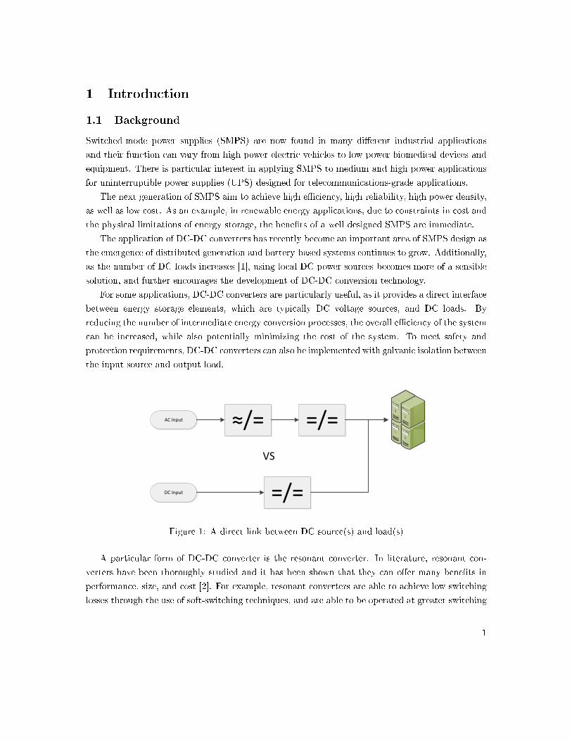
1 Introduction
1.1 Background
Switched-mode power supplies (SMPS) are now found in many di�erent industrial applications
and their function can vary from high power electric vehicles to low power biomedical devices and
equipment. There is particular interest in applying SMPS to medium and high power applications
for uninterruptible power supplies (UPS) designed for telecommunications-grade applications.
The next generation of SMPS aim to achieve high e�ciency, high reliability, high power density,
as well as low cost. As an example, in renewable energy applications, due to constraints in cost and
the physical limitations of energy storage, the bene�ts of a well designed SMPS are immediate.
The application of DC-DC converters has recently become an important area of SMPS design as
the emergence of distributed generation and battery-based systems continues to grow. Additionally,
as the number of DC loads increases [1], using local DC power sources becomes more of a sensible
solution, and further encourages the development of DC-DC conversion technology.
For some applications, DC-DC converters are particularly useful, as it provides a direct interface
between energy storage elements, which are typically DC voltage sources, and DC loads. By
reducing the number of intermediate energy conversion processes, the overall e�ciency of the system
can be increased, while also potentially minimizing the cost of the system. To meet safety and
protection requirements, DC-DC converters can also be implemented with galvanic isolation between
the input source and output load.
AC Input ≈/= =/=
DC Input =/=
VS
Figure 1: A direct link between DC source(s) and load(s)
A particular form of DC-DC converter is the resonant converter. In literature, resonant con-
verters have been thoroughly studied and it has been shown that they can o�er many bene�ts in
performance, size, and cost [2]. For example, resonant converters are able to achieve low switching
losses through the use of soft-switching techniques, and are able to be operated at greater switching
1

frequencies than other comparable converters.
The ability to operate at higher switching frequencies has the superior advantage of increasing
e�ciency, as well as decreasing the size of the discrete components, notably inductors and capacitors,
within the hardware. This is in comparison to pulse-width modulation (PWM) converters, where
the turn-on and turn-o� losses of the switching devices at high switching frequencies can be high
enough to prohibit operation of the converter, even when soft-switching techniques are used [3].
Moreover, PWM converters utilizing high switching frequency operation can cause disturbances
such as electromagnetic interference (EMI) and su�er from the e�ects of parasitic impedances.
However, under proper design, it is possible for resonant converters to utilize the leakage inductances
of the circuit as part of the resonant tank circuit. It was also found that certain resonant converters
are able to operate with low EMI [4]. Because of these advantages, resonant converters with
switching frequencies in the range of MHz are conceivable [2][5].
Some typical resonant topologies include the series resonant, parallel resonant, and the series-
parallel resonant converters.
1.2 Motivation
Because of the demand for resonant conversion, methods on how to design e�ective feedback con-
trol systems for resonant converters becomes a topic of considerable interest. To make a converter
valuable for practical system applications, and to achieve speci�cations such as output voltage regu-
lation, it is necessary to adopt some form of feedback control. Furthermore, with the advancements
in digital signal processors, digital control techniques have become a feasible option. The applica-
tion of digital controllers has allowed for more �exible designs when compared to analog controllers,
and allows for much greater reliability and system integration.
Consequently, this thesis will be centered around designing and implementing a digital control
system for a resonant power electronics converter topology to be used in a medium power appli-
cation. Chapter 2 will discuss in detail a resonant converter topology, followed by discussion on
implementing a digitally controlled negative feedback control loop for output voltage regulation in
Chapters 3 and 4. Lastly, a novel mathematical model of the small signal control-to-output transfer
function is presented in Chapter 5.
2
2 LLC Resonant Converter
Resonant power converters contain L-C networks, or resonant tanks, whose voltage and current
waveforms vary sinusoidally during one or more subintervals of each switching period [6]. Three
well-known resonant topologies include the series resonant, parallel resonant, and series-parallel
resonant. Although there are peculiar di�erences in each of these topologies, the essential operation
is the same: a square pulse of voltage or current is generated, and applied to the resonant tank
circuit. Energy circulating within the resonant tank will then either be fully supplied to the output
load, or be dissipated within the tank circuit [2].
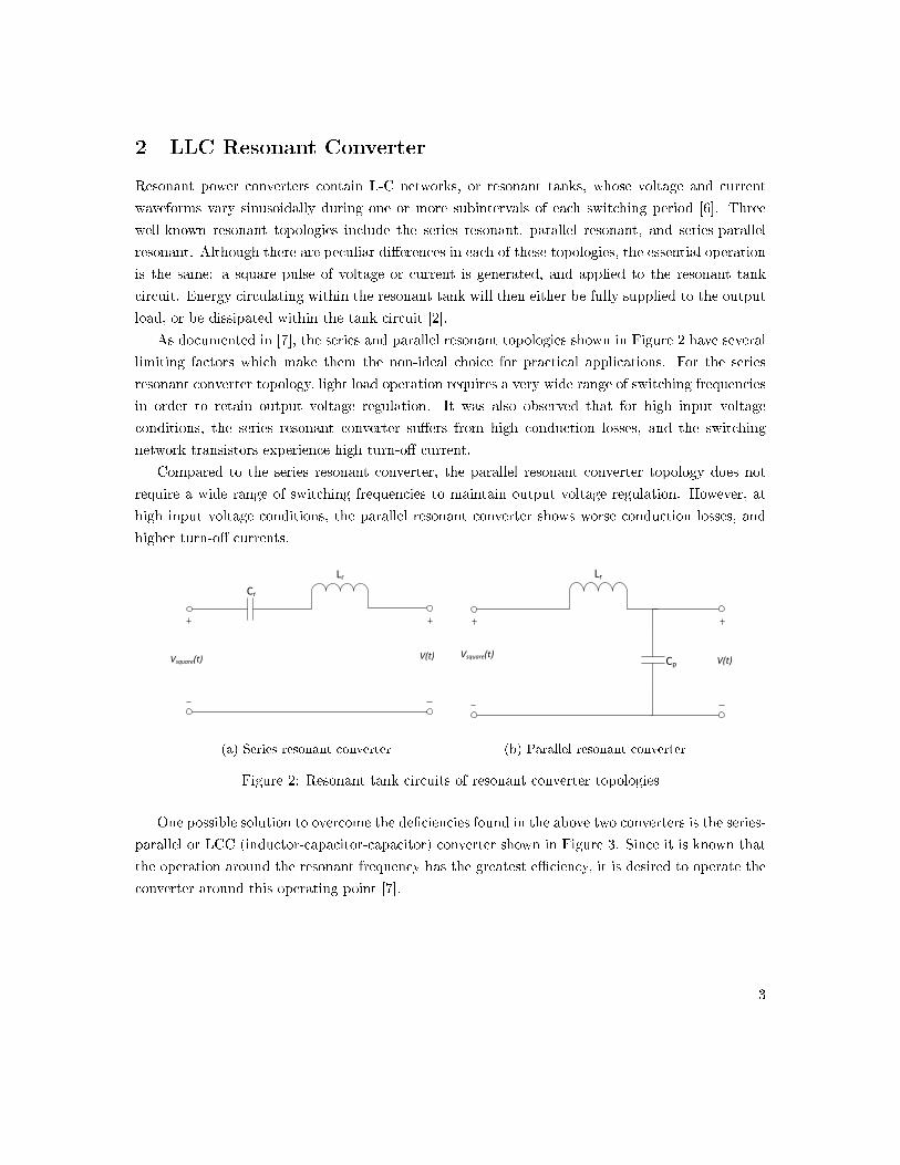
As documented in [7], the series and parallel resonant topologies shown in Figure 2 have several
limiting factors which make them the non-ideal choice for practical applications. For the series
resonant converter topology, light load operation requires a very wide range of switching frequencies
in order to retain output voltage regulation. It was also observed that for high input voltage
conditions, the series resonant converter su�ers from high conduction losses, and the switching
network transistors experience high turn-o� current.
Compared to the series resonant converter, the parallel resonant converter topology does not
require a wide range of switching frequencies to maintain output voltage regulation. However, at
high input voltage conditions, the parallel resonant converter shows worse conduction losses, and
higher turn-o� currents.
Cr
Lr
CpVsquare(t) V(t)
Cr
Lr
V(t)Vsquare(t)
Lr
Cp V(t)Vsquare(t)
(a) Series resonant converter
Cr
Lr
CpVsquare(t) V(t)
Cr
Lr
V(t)Vsquare(t)
Lr
Cp V(t)Vsquare(t)
(b) Parallel resonant converter
Figure 2: Resonant tank circuits of resonant converter topologies
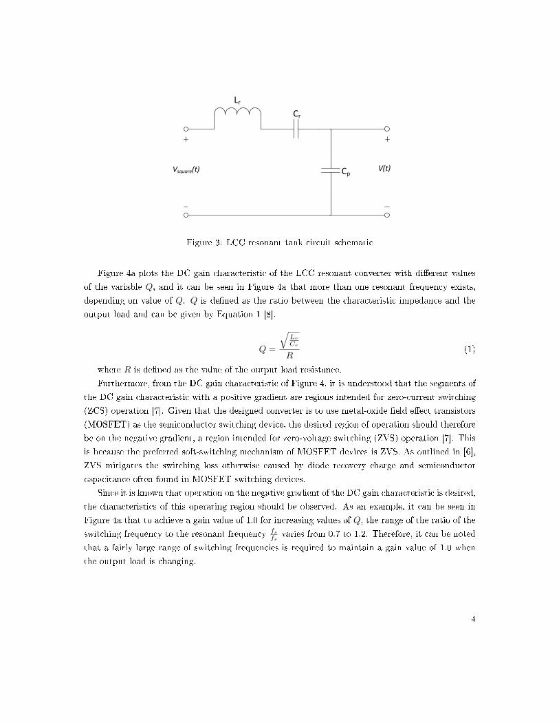
One possible solution to overcome the de�ciencies found in the above two converters is the series-
parallel or LCC (inductor-capacitor-capacitor) converter shown in Figure 3. Since it is known that
the operation around the resonant frequency has the greatest e�ciency, it is desired to operate the
converter around this operating point [7].
3
Lr
CpVsquare(t) V(t)
Cr
Lr
V(t)Vsquare(t)
Lr
Cp V(t)Vsquare(t)Cr
Figure 3: LCC resonant tank circuit schematic
Figure 4a plots the DC gain characteristic of the LCC resonant converter with di�erent values
of the variable Q, and it can be seen in Figure 4a that more than one resonant frequency exists,
depending on value of Q. Q is de�ned as the ratio between the characteristic impedance and the
output load and can be given by Equation 1 [8].
Q =
√Lr
Cr
R(1)
where R is de�ned as the value of the output load resistance.
Furthermore, from the DC gain characteristic of Figure 4, it is understood that the segments of
the DC gain characteristic with a positive gradient are regions intended for zero-current switching
(ZCS) operation [7]. Given that the designed converter is to use metal-oxide �eld e�ect transistors
(MOSFET) as the semiconductor switching device, the desired region of operation should therefore
be on the negative gradient, a region intended for zero-voltage switching (ZVS) operation [7]. This
is because the preferred soft-switching mechanism of MOSFET devices is ZVS. As outlined in [6],
ZVS mitigates the switching loss otherwise caused by diode recovery charge and semiconductor
capacitance often found in MOSFET switching devices.
Since it is known that operation on the negative gradient of the DC gain characteristic is desired,
the characteristics of this operating region should be observed. As an example, it can be seen in
Figure 4a that to achieve a gain value of 1.0 for increasing values of Q, the range of the ratio of the
switching frequency to the resonant frequency fsfr
varies from 0.7 to 1.2. Therefore, it can be noted
that a fairly large range of switching frequencies is required to maintain a gain value of 1.0 when
the output load is changing.
4
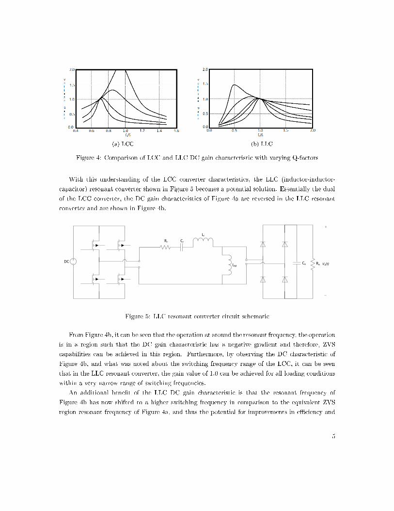
(a) LCC (b) LLC
Figure 4: Comparison of LCC and LLC DC gain characteristic with varying Q-factors
With this understanding of the LCC converter characteristics, the LLC (inductor-inductor-
capacitor) resonant converter shown in Figure 5 becomes a potential solution. Essentially the dual
of the LCC converter, the DC gain characteristics of Figure 4a are reversed in the LLC resonant
converter and are shown in Figure 4b.
Vsquare(t)
Vo(t)
V(t)
Vsquare(t) V(t)DC
Rr Cr
Lr
LMDC Co Ro
Vo(t)Co Ro
Rac Vo(t)
z-1
z-1
z-1
z-1
+ +
+ +
u(k)e(k)b0
b1
b2
-a1
-a2
V(t)
Rr Cr
Lr
LMV(t)
Rr Cr
Rac
Lr
LM
Figure 5: LLC resonant converter circuit schematic
From Figure 4b, it can be seen that the operation at around the resonant frequency, the operation
is in a region such that the DC gain characteristic has a negative gradient and therefore, ZVS
capabilities can be achieved in this region. Furthermore, by observing the DC characteristic of
Figure 4b, and what was noted about the switching frequency range of the LCC, it can be seen
that in the LLC resonant converter, the gain value of 1.0 can be achieved for all loading conditions
within a very narrow range of switching frequencies.
An additional bene�t of the LLC DC gain characteristic is that the resonant frequency of
Figure 4b has now shifted to a higher switching frequency in comparison to the equivalent ZVS
region resonant frequency of Figure 4a, and thus the potential for improvements in e�ciency and
5
power density are greatly improved.
Some other advantages of the LLC resonant converter over other resonant topologies is its ability
to maintain ZVS characteristics under light load conditions, and low electromagnetic interference
(EMI) [4].
Since it has now been determined that the LLC resonant converter has many favorable features
for DC-DC conversion applications, Sections 2.1 - 2.4 will discuss each stage of the LLC resonant
converter, as well as the theory of operation.
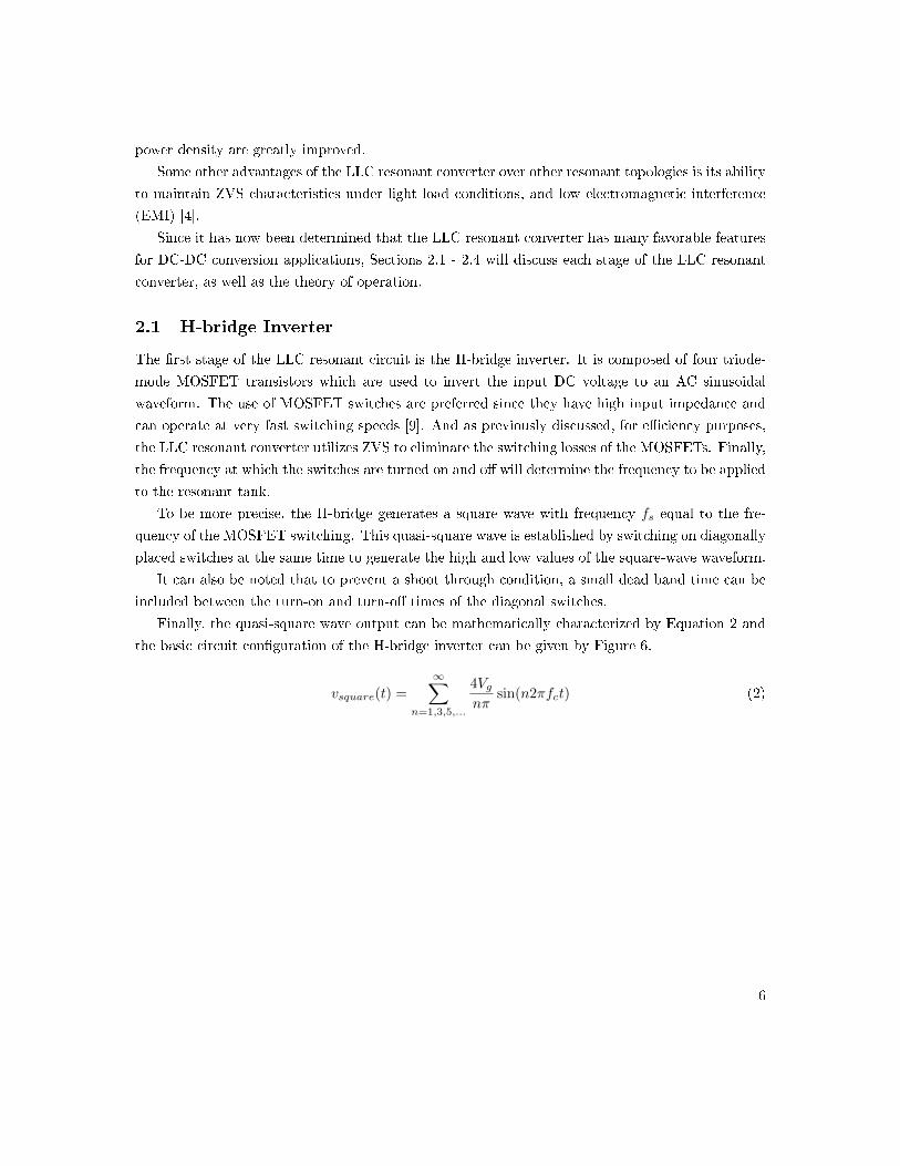
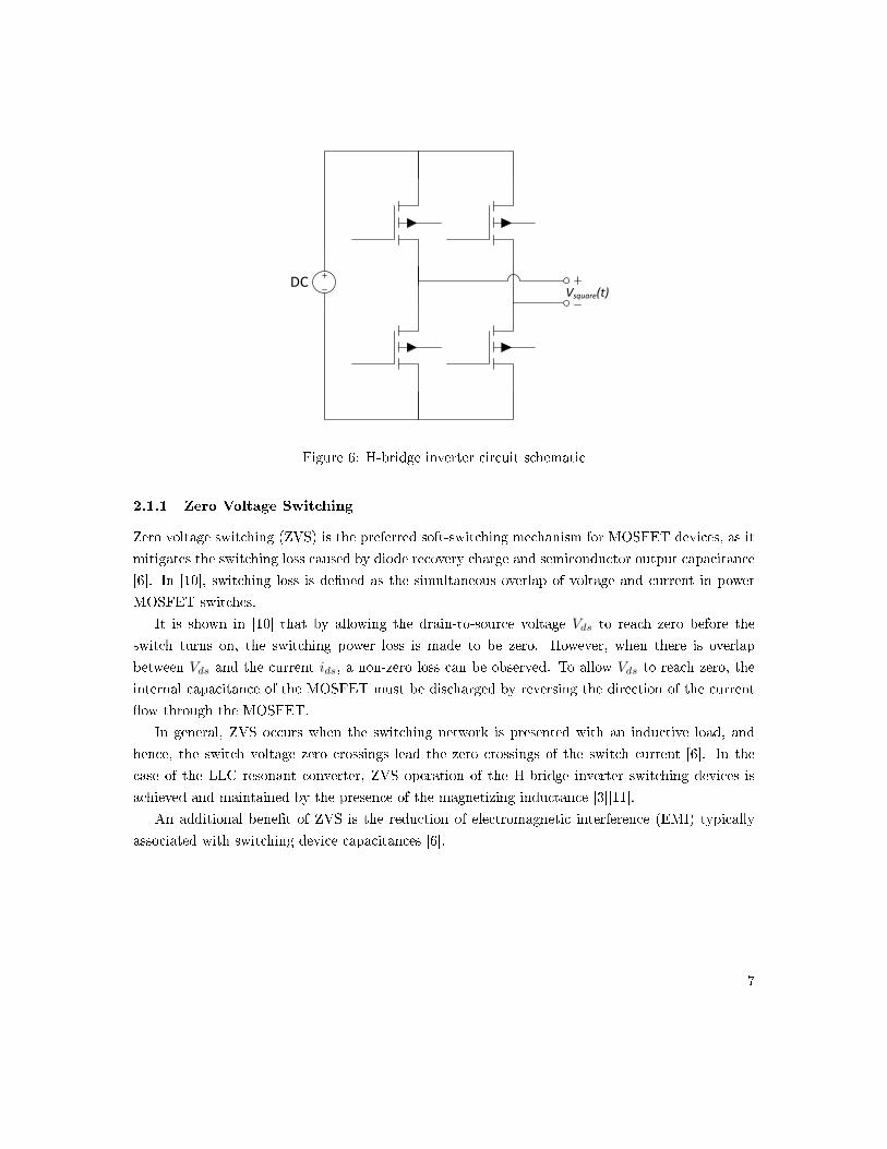
2.1 H-bridge Inverter
The �rst stage of the LLC resonant circuit is the H-bridge inverter. It is composed of four triode-
mode MOSFET transistors which are used to invert the input DC voltage to an AC sinusoidal
waveform. The use of MOSFET switches are preferred since they have high input impedance and
can operate at very fast switching speeds [9]. And as previously discussed, for e�ciency purposes,
the LLC resonant converter utilizes ZVS to eliminate the switching losses of the MOSFETs. Finally,
the frequency at which the switches are turned on and o� will determine the frequency to be applied
to the resonant tank.
To be more precise, the H-bridge generates a square wave with frequency fs equal to the fre-
quency of the MOSFET switching. This quasi-square wave is established by switching on diagonally
placed switches at the same time to generate the high and low values of the square-wave waveform.
It can also be noted that to prevent a shoot through condition, a small dead band time can be
included between the turn-on and turn-o� times of the diagonal switches.
Finally, the quasi-square wave output can be mathematically characterized by Equation 2 and
the basic circuit con�guration of the H-bridge inverter can be given by Figure 6.
vsquare(t) =
∞∑n=1,3,5,...
4Vgnπ
sin(n2πfct) (2)
6
Vsquare(t)
Vo(t)
V(t)
Vsquare(t) V(t)DC
Rr Cr
Lr
LMDC Co Ro
Vo(t)Co Ro
Rac Vo(t)
z-1
z-1
z-1
z-1
+ +
+ +
u(k)e(k)b0
b1
b2
-a1
-a2
V(t)
Rr Cr
Lr
LMV(t)
Rr Cr
Rac
Lr
LM
Figure 6: H-bridge inverter circuit schematic
2.1.1 Zero Voltage Switching
Zero voltage switching (ZVS) is the preferred soft-switching mechanism for MOSFET devices, as it
mitigates the switching loss caused by diode recovery charge and semiconductor output capacitance
[6]. In [10], switching loss is de�ned as the simultaneous overlap of voltage and current in power
MOSFET switches.
It is shown in [10] that by allowing the drain-to-source voltage Vds to reach zero before the
switch turns on, the switching power loss is made to be zero. However, when there is overlap
between Vds and the current ids, a non-zero loss can be observed. To allow Vds to reach zero, the
internal capacitance of the MOSFET must be discharged by reversing the direction of the current
�ow through the MOSFET.
In general, ZVS occurs when the switching network is presented with an inductive load, and
hence, the switch voltage zero crossings lead the zero crossings of the switch current [6]. In the
case of the LLC resonant converter, ZVS operation of the H-bridge inverter switching devices is
achieved and maintained by the presence of the magnetizing inductance [3][11].
An additional bene�t of ZVS is the reduction of electromagnetic interference (EMI) typically
associated with switching device capacitances [6].
7
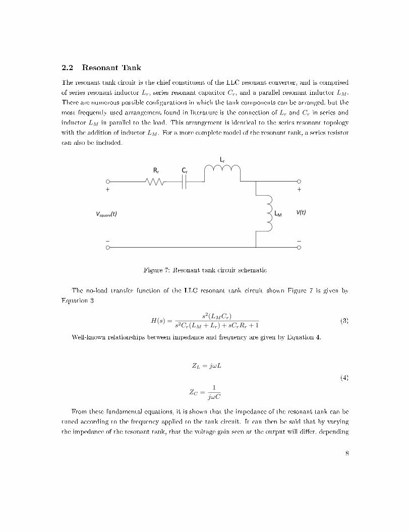
2.2 Resonant Tank
The resonant tank circuit is the chief constituent of the LLC resonant converter, and is comprised
of series resonant inductor Lr, series resonant capacitor Cr, and a parallel resonant inductor LM .
There are numerous possible con�gurations in which the tank components can be arranged, but the
most frequently used arrangement found in literature is the connection of Lr and Cr in series and
inductor LM in parallel to the load. This arrangement is identical to the series resonant topology
with the addition of inductor LM . For a more complete model of the resonant tank, a series resistor
can also be included.
Vsquare(t)
Vo(t)
V(t)
Vsquare(t) V(t)DC
Rr Cr
Lr
LMDC Co Ro
Vo(t)Co Ro
Rac Vo(t)
z-1
z-1
z-1
z-1
+ +
+ +
u(k)e(k)b0
b1
b2
-a1
-a2
V(t)
Rr Cr
Lr
LMV(t)
Rr Cr
Rac
Lr
LM
Figure 7: Resonant tank circuit schematic
The no-load transfer function of the LLC resonant tank circuit shown Figure 7 is given by
Equation 3
H(s) =s2(LMCr)
s2Cr(LM + Lr) + sCrRr + 1(3)
Well-known relationships between impedance and frequency are given by Equation 4.
ZL = jωL
(4)
ZC =1
jωC
From these fundamental equations, it is shown that the impedance of the resonant tank can be
tuned according to the frequency applied to the tank circuit. It can then be said that by varying
the impedance of the resonant tank, that the voltage gain seen at the output will di�er, depending
8
on the frequency applied to the resonant tank. It is then concluded that this voltage gain will
determine the attainable output voltage value, and thus is the method in which output voltage
regulation can be achieved with the LLC resonant converter.
2.2.1 Resonant Frequencies ωr1,ωr2
From the values of Lr, Cr, and LM , two important operating conditions can be identi�ed: ωr1 and
ωr2. These operating points are de�ned as the resonant frequencies, and are de�ned by the applied
loading condition. From Figure 7, it can be seen that at the no-load condition, the inductance
LM is seen by the tank circuit as a passive load and thus, the resonant frequency can be given by
Equation 5.
ωr2 =1√
(Lr + LM )Cr(5)
In the case where a nominal load is applied, the load seen by the resonant tank is e�ectively the
large output capacitance Co in parallel with inductance LM . Thus, the inductor LM is bypassed
by the e�ective AC short circuit and the resonant frequency can be given by Equation 6.
ωr1 =1√LrCr
(6)
In this thesis, operation is focused around the resonant frequency given by Equation 6, as this
operating point allows for greater e�ciency, and allows for regulation using only a narrow range of
switching frequencies.
2.2.2 High Frequency Isolation Transformer
Following the resonant tank circuit is a high frequency isolation transformer that can be used to
either buck or boost the sinusoidal voltage to the secondary side of the converter. The transformer
also serves the dual purpose of providing galvanic isolation, such that no direct current �ows between
the input and output.
A rather remarkable feature of the transformer is that the magnetizing and leakage inductances
can be used as part of the tank circuit. For instance, the magnetizing inductance of the transformer
can be used as or part of the parallel resonant inductance LM , therefore potentially reducing the
number of additional discrete components required. Similarly, the leakage inductance can be made
a part of the series inductor Lr, depending on the design of the transformer parameters. This so-
called integrated magnetic can therefore be designed to serve the purpose of potentially increasing
the converter's power density.
The transformer ratio between the primary and secondary sides is given by the transformer
turns ratio and shown by Equation 7.
9
N =NsecondaryNprimary
(7)
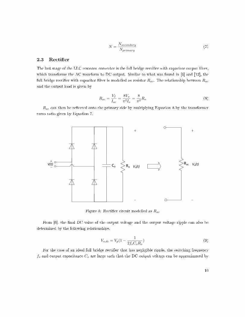
2.3 Recti�er
The last stage of the LLC resonant converter is the full bridge recti�er with capacitor output �lter,
which transforms the AC waveform to DC output. Similar to what was found in [6] and [12], the
full bridge recti�er with capacitor �lter is modelled as resistor Rac. The relationship between Rac
and the output load is given by
Rac =VIIac
=8Voπ2Io
=8
π2Ro (8)
Rac can then be re�ected onto the primary side by multiplying Equation 8 by the transformer
turns ratio given by Equation 7.
Vsquare(t)
Vo(t)
V(t)
Vsquare(t) V(t)DC
Rr Cr
Lr
LMDC Co Ro
Vo(t)Co Ro
Rac Vo(t)
z-1
z-1
z-1
z-1
+ +
+ +
u(k)e(k)b0
b1
b2
-a1
-a2
V(t)
Rr Cr
Lr
LMV(t)
Rr Cr
Rac
Lr
LM
Figure 8: Recti�er circuit modelled as Rac
From [6], the �nal DC value of the output voltage and the output voltage ripple can also be
determined by the following relationships.
Vo,dc = Vp(1−1
2fsCoRo) (9)
For the case of an ideal full bridge recti�er that has negligible ripple, the switching frequency
fs and output capacitance Co are large such that the DC output voltage can be approximated by
10
Equation 10.
Vo,dc ≈ Vp (10)
where Vp is the peak value of the AC input voltage, V (t).
2.3.1 Synchronous Recti�cation
To further increase the e�ciency of the LLC resonant converter, a synchronous recti�cation (SR)
network can be implemented in lieu of the full bridge diode recti�er. In a synchronous recti�er,
the diodes are replaced with MOSFET devices, and when current �ow is detected on the secondary
side, the MOSFETs are turned on to allow current �ow to the load.
This is a much more e�cient strategy in comparison to the diode recti�er, as the voltage drop
across the diode is eliminated. Additionally, unlike diodes, which are only able to provide unidirec-
tional �ow of power, a SR network makes bidirectional power �ow between the input and output
feasible.
The disadvantage of implementing SR with the LLC resonant converter is the increased com-
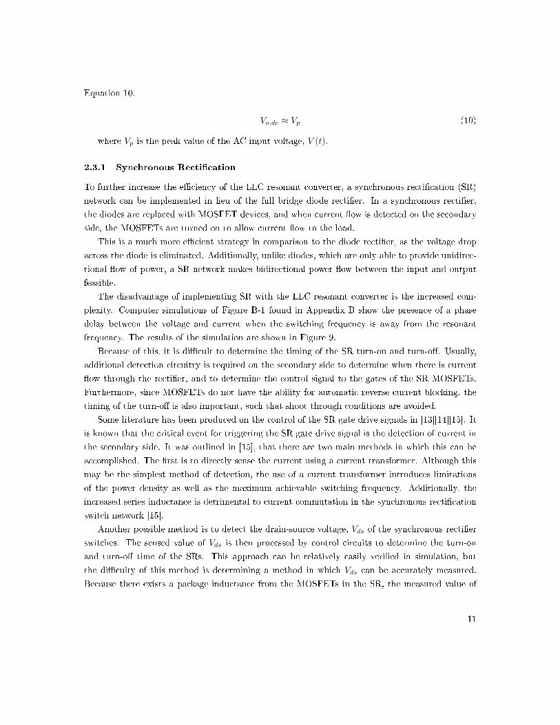
plexity. Computer simulations of Figure B-1 found in Appendix B show the presence of a phase
delay between the voltage and current when the switching frequency is away from the resonant
frequency. The results of the simulation are shown in Figure 9.
Because of this, it is di�cult to determine the timing of the SR turn-on and turn-o�. Usually,
additional detection circuitry is required on the secondary side to determine when there is current
�ow through the recti�er, and to determine the control signal to the gates of the SR MOSFETs.
Furthermore, since MOSFETs do not have the ability for automatic reverse current blocking, the
timing of the turn-o� is also important, such that shoot through conditions are avoided.
Some literature has been produced on the control of the SR gate drive signals in [13][14][15]. It
is known that the critical event for triggering the SR gate drive signal is the detection of current in
the secondary side. It was outlined in [15], that there are two main methods in which this can be
accomplished. The �rst is to directly sense the current using a current transformer. Although this
may be the simplest method of detection, the use of a current transformer introduces limitations
of the power density as well as the maximum achievable switching frequency. Additionally, the
increased series inductance is detrimental to current commutation in the synchronous recti�cation
switch network [15].
Another possible method is to detect the drain-source voltage, Vds of the synchronous recti�er
switches. The sensed value of Vds is then processed by control circuits to determine the turn-on
and turn-o� time of the SRs. This approach can be relatively easily veri�ed in simulation, but
the di�culty of this method is determining a method in which Vds can be accurately measured.
Because there exists a package inductance from the MOSFETs in the SR, the measured value of
11
C:\Users\Brian\Documents\PSIM\difference_eq_CL_May17.smvDate: 05:07PM 09/27/12
0
-50
-100
-150
50
100
150
Vtank Itra
(a) Voltage and current waveforms in phase when fs = fr1C:\Users\Brian\Documents\PSIM\difference_eq_CL_May17.smv
Date: 05:08PM 09/27/12
0
-20
-40
-60
20
40
60
Vtank Itra
(b) Voltage and current waveforms out of phase when fs 6= fr1
Figure 9: SR phase delay
12
Vds becomes highly deviated if the package inductance is not properly considered. If the physically
sensed value is far deviated from the true value of Vds, a false trigger of the SR circuits may occur,
and the potential for shoot through condition increases.
Some literature proposed by [13][14], have shown a number of methods to improve the accuracy
of sensing Vds. This is at the expense of circuit complexity, as several additional compensating
components are required.
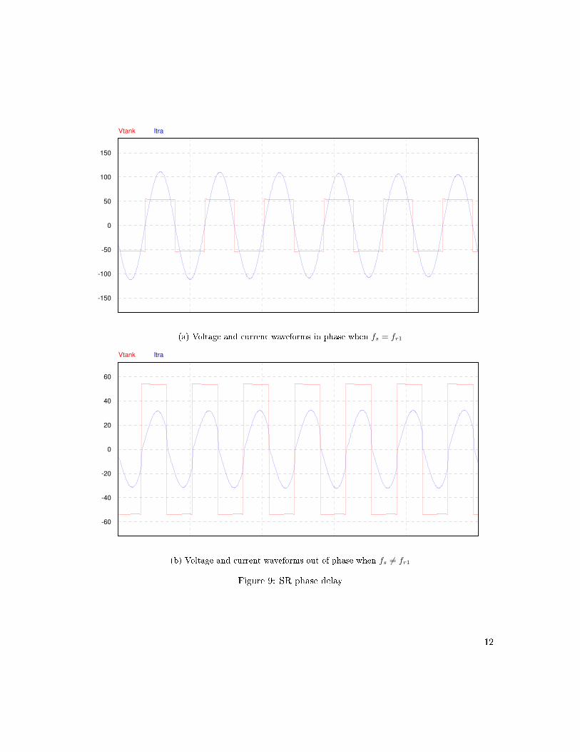
A computer simulation using a current-sensing method has been proposed and is shown in
Figure 10.
Title
Designed by
Revision Page 1 of 2
V
Vout
A
Isec
Vmos3
Vmos1 Vmos3
Vmos1
A
Iload
Imos3
Imos1V
Vmos1
V
Vmos3
Vmos1
Vmos3
Figure 10: Synchronous recti�cation PSIM R© model
13
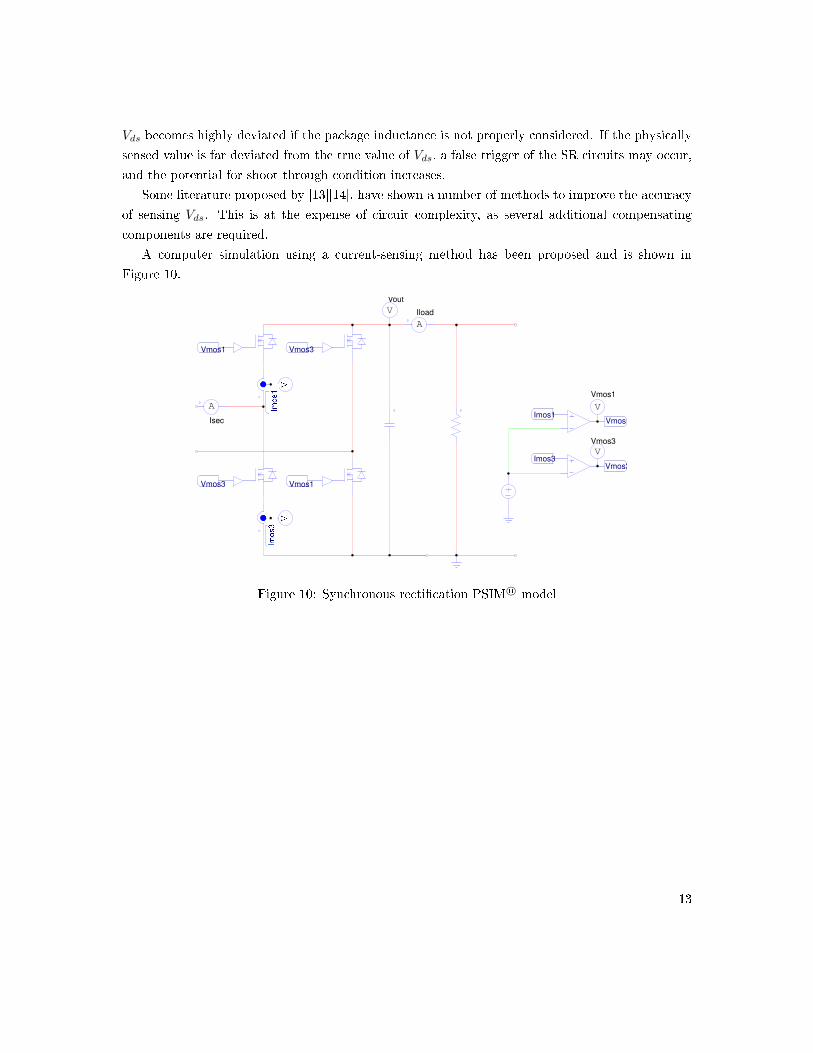
2.4 Theory of Operation
The fundamental operation of the LLC resonant converter is based on applying a voltage with
frequency fs to the resonant tank to vary the impedance of the tank circuit, thus controlling the
achievable gain seen at the output. From Figure 11, it can be seen that as the switching frequency is
increased, the output gain is decreasing. This implies that as the switching frequency is increased,
the impedance of the resonant tank is increased, and therefore, a larger voltage drop is observed
across the resonant tank circuit components, and less voltage is transferred to the load. The reverse
is true as well, such that as the switching frequency decreases, the DC gain increases, implying that
the voltage drop across the tank circuit has decreased, and the output voltage gain can be increased.
In the following sections, the operation of the LLC resonant converter is more closely considered,
and a single switching interval is analyzed.
There are three main regions of operation, commonly described as Region 1, 2, and 3. Operation
in Region 1, 2, and 3 is determined by the location of the operating point on the DC gain curve
shown in Figure 11. Region 1 and 2 are located on the negative gradient of the DC gain curve, and
Region 3 is located on the positive gradient. Region 1 is the set of switching frequencies greater
than the resonant frequency, while Region 2 is the set of switching frequencies below the resonant
frequency.
Figure 11: Regions 1, 2, and 3
Depending on the design speci�cations and requirements that are desired, operation in any of
these regions is possible. As it is preferred to switch the MOSFET devices under ZVS conditions,
the focus will be on operation in Regions 1 and 2, which is graphically shown in Figure 11 as the
negative gradients of the DC gain curves.
14
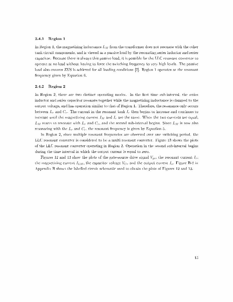
2.4.1 Region 1
In Region 1, the magnetizing inductance LM from the transformer does not resonate with the other
tank circuit components, and is viewed as a passive load by the resonating series inductor and series
capacitor. Because there is always this passive load, it is possible for the LLC resonant converter to
operate at no load without having to force the switching frequency to very high levels. The passive
load also ensures ZVS is achieved for all loading conditions [7]. Region 1 operates at the resonant
frequency given by Equation 6.
2.4.2 Region 2
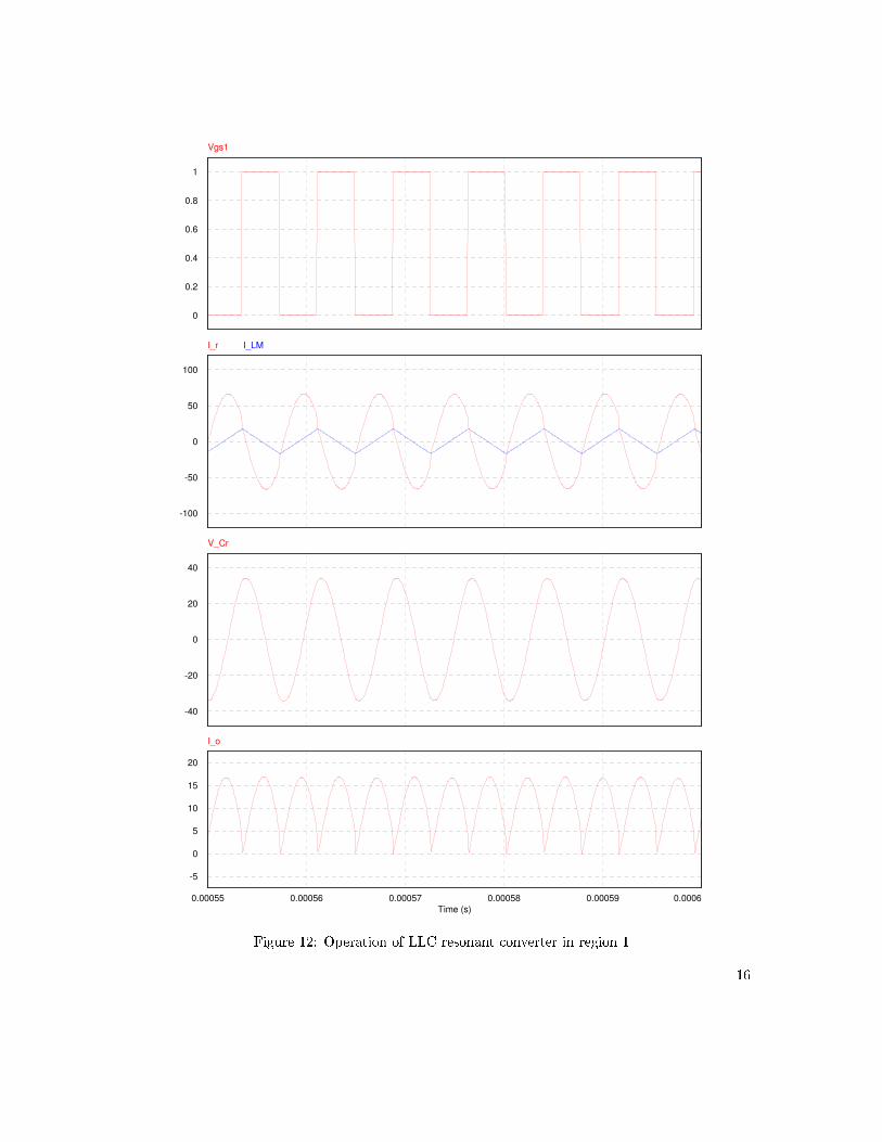
In Region 2, there are two distinct operating modes. In the �rst time sub-interval, the series
inductor and series capacitor resonate together while the magnetizing inductance is clamped to the
output voltage, and has operation similar to that of Region 1. Therefore, the resonance only occurs
between Lr and Cr. The current in the resonant tank Ir then begins to increase and continues to
increase until the magnetizing current IM and Ir are the same. When the two currents are equal,
LM starts to resonate with Lr and Cr, and the second sub-interval begins. Since LM is now also
resonating with the Lr and Cr, the resonant frequency is given by Equation 5.
In Region 2, since multiple resonant frequencies are observed over one switching period, the
LLC resonant converter is considered to be a multi-resonant converter. Figure 13 shows the plots
of the LLC resonant converter operating in Region 2. Operation in the second sub-interval begins
during the time interval in which the output current is equal to zero.
Figures 12 and 13 show the plots of the gate-source drive signal Vgs, the resonant current Ir,
the magnetizing current ILM , the capacitor voltage VCr and the output current Io. Figure B-2 in
Appendix B shows the labelled circuit schematic used to obtain the plots of Figures 12 and 13.
15
C:\Users\Brian\Documents\PSIM\difference_eq_CL_May17.smvDate: 05:22PM 09/27/12
0
0.2
0.4
0.6
0.8
1
Vgs1
0
-50
-100
50
100
I_r I_LM
0
-20
-40
20
40
V_Cr
0.00055 0.00056 0.00057 0.00058 0.00059 0.0006
Time (s)
0
-5
5
10
15
20
I_o
Figure 12: Operation of LLC resonant converter in region 1
16
C:\Users\Brian\Documents\PSIM\difference_eq_CL_May17.smvDate: 05:23PM 09/27/12
0
0.2
0.4
0.6
0.8
1
Vgs1
0
-100
-200
100
200
I_r I_LM
0
-50
-100
50
100
V_Cr
0.00055 0.00056 0.00057 0.00058 0.00059 0.0006
Time (s)
0
-10
10
20
30
40
50
I_o
Figure 13: Operation of LLC resonant converter in region 2
17
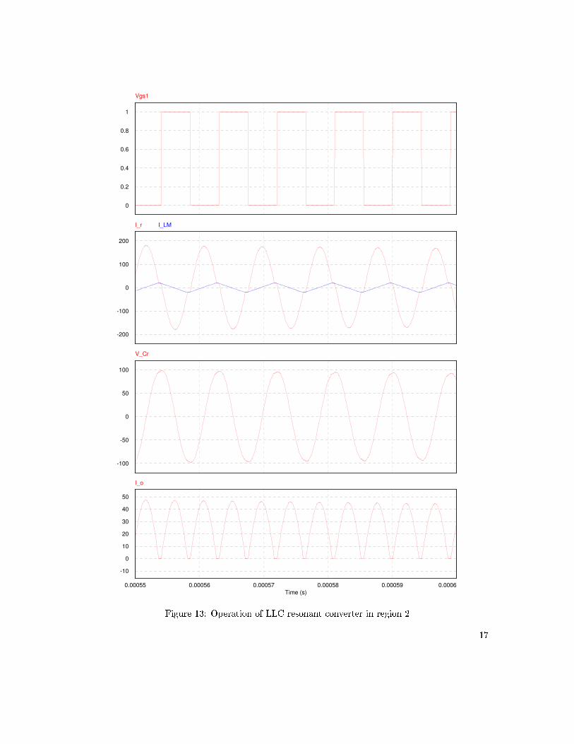
3 Control of LLC Resonant Converter
When correctly applied, the application of control theory and feedback can eliminate steady state
errors, moderate system sensitivity to parameter changes and disturbances, modify the gain or
phase of the system over a desired frequency range, and make unstable systems stable.
For this thesis, the objective is to design a voltage control loop to regulate the output voltage,
according to a prede�ned reference voltage. In other words, regardless of disturbances to the system,
and more speci�cally, the load; the output voltage is to remain at a constant value. Consequently,
a negative feedback loop was designed to achieve these speci�cations.
Compensation Network
G(s)
Actuator(VCO)
Switching ConverterP(s)
Sensor Gain
+-
e
y
Reference Inputr
Disturbances
Vo
Digital Compensator
D(s)
Actuator(VCO)
u
Analog-to-Digital Converter
+-
e
y
Reference Inputr
PlantP(s)
Digital-to-Analog Converter
Sensor Gain
Figure 14: Block diagram of negative feedback loop
From Figure 14, it can be seen that the function of the negative feedback control loop is to
determine an input to the plant, such that the desired output behavior can be obtained. Speci�cally,
for the LLC resonant converter, the objective is to generate a set of gate driving signals of frequency
fs for the primary side switch network.
Figure 14 shows that by sensing the output y and comparing it to reference input r, the com-
pensator network G(s) can generate the gate drive signals based on the given error signal e. The
error signal is the di�erence between the y and r, and in a functional control loop, tends to zero
after some time period.
3.0.3 Variable Frequency Control
Under normal operating conditions, the LLC resonant converter uses variable frequency control to
regulate the output voltage. This type of control requires a gate drive signal that has constant duty
cycle, but varying frequency.
18
To implement variable frequency control, an actuator that can produce a variable frequency
signal is required and can be realized by a voltage controlled oscillator (VCO). The VCO is an
electronic circuit designed to produce an oscillation frequency based on the control voltage Vctrl
and can be implemented as an analog circuit or with a digital signal processor. The relationship
between the input signal Vctrl and the output frequency signal ωo is shown in Equation 11.
ωo = ω̂ −KV COVctrl (11)
In Equation 11, ω̂ is the free-running frequency of the VCO, and KV CO is the gain of the voltage
controlled oscillator.
3.0.4 Pulse Width Modulation
Pulse-width modulation (PWM) is a �xed frequency control method, and modi�es the duty cycle
of the pulses to regulate the output voltage. It has been suggested in the literature [16][17] that for
light and no load conditions that it may be more e�ective to control the LLC resonant converter
by using PWM rather than variable frequency control. However, in this work, it will be assumed
that the converter always operates under nominal loading conditions, and therefore only requires
the use of the variable frequency control method.
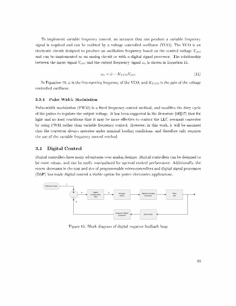
3.1 Digital Control
Digital controllers have many advantages over analog designs. Digital controllers can be designed to
be more robust, and can be easily manipulated for optimal control performance. Additionally, the
recent decreases in the cost and size of programmable micro-controllers and digital signal processors
(DSP) has made digital control a viable option for power electronics applications.
Compensation Network
G(s)
Actuator(VCO)
Switching ConverterP(s)
Sensor Gain
+-
e
y
Reference Inputr
Disturbances
Vo
Digital Compensator
D(s)
Actuator(VCO)
u
Analog-to-Digital Converter
+-
e
y
Reference Inputr
PlantP(s)
Digital-to-Analog Converter
Sensor Gain
Figure 15: Block diagram of digital negative feedback loop
19
3.1.1 E�ects of Sampling Frequency
An essential consideration that is relevant to digital systems is the principle of sampling, a non-zero
timed event to capture the continuous-time data. Sampling is required to convert continuous-time
data to discrete-time for processing in the digital signal processor and is physically realized with
an analog-to-digital (A/D) converter. The aim of the A/D converter is to accept measured signals
from the output of the power electronic converter and then convert these signals into an electrical
voltage level that can be read by the DSP. Conversely, once the processing has been completed in
the DSP, a digital-to-analog (D/A) converter is used to produce a physical signal to be read by the
power electronic converter.
A crucial factor in digital design is the sampling rate at which the continuous-time signal is
sampled. Ideally, the sampling rate is in�nite such that the discrete-time system is equivalent to
the continuous-time model. Unfortunately, since this is not a realistic solution, the alternative
solution is to apply the Nyquist rate shown in Equation 12.
fsample ≥ 2fmax (12)
The Nyquist rate states that the sampling frequency must be at least twice the maximum band-
width in the system. By satisfying this criterion, aliasing and signal distortion in the reconstructed
signal can be avoided. It can be added that, in fact, it is recommended in [6] to make the sampling
frequency ten times the maximum bandwidth.
3.1.2 Design of Digital Control Systems
Digital controllers can be implemented using two primary methods: emulation and direct digital
design.
Digital controllers designed through emulation method use the continuous-time plant model, and
obtain the compensator model in continuous-time. The continuous-time s-domain model is then
converted to a discrete-time z-domain compensator by applying mathematical transformations.
Numerous methods to transform continuous-time transfer functions to discrete-time transfer
functions exists. Some typical methods include the Tustin method, zero-order hold, �rst-order
hold, etc. From [18], it was found that for the most accurate models, the �rst-order hold is the
most accurate discretization method, but at the expense of computational complexity. A more
general method that is typically used is the zero-order hold discretization as it provides a balance
of accuracy and computational e�ciency.
The advantage of the emulation method is that well-developed and familiar continuous-time
design methods can be applied. This method produces reasonably accurate results given that the
sampling rate is very fast. The main disadvantage of the emulation method is that after mapping
20
the compensator from continuous to discrete-time, it is possible that the control system can no
longer achieve the same performance characteristics as in the continuous-time domain model [18].
The other method which can be used to design a digital compensator is by using the direct
digital design methodology. Compensators implemented using the direct digital design technique
usually have signi�cantly better performance when implemented on digital signal processors. This
method of design immediately begins with a plant model already in discrete-time, and then the
compensator is designed based o� the digitized plant model in the z-domain [19]. Thus, the proba-
bility of obtaining unexpected controller response and dynamics are mitigated when the controller
is implemented using a DSP.
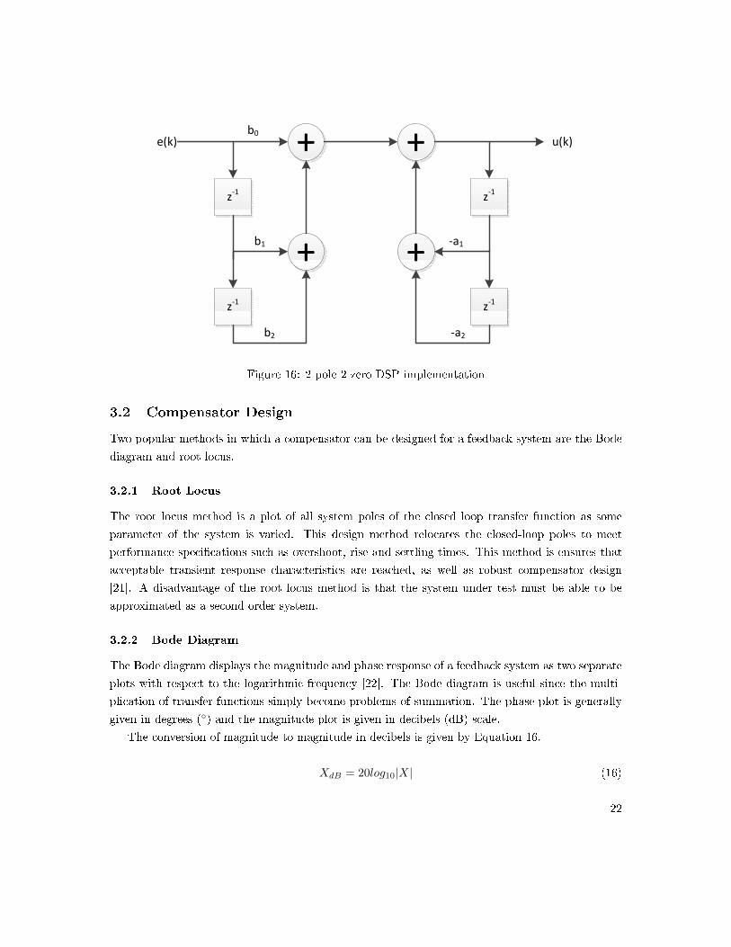
3.1.3 2-Pole-2-Zero Compensator
Irrespective of which compensator design method is used, the end goal is to design a compensator
G(s) to supply the correct signals to maintain output voltage regulation. Loop compensation is
achieved by the placement of additional poles and zeros to the feedback system, in conjunction
with the system's natural poles and zeros. The system loop gain can then be shaped to the desired
performance and stability characteristics by the new poles and zeros introduced to the system. An
example of compensator in the digital domain is the 2-pole-2-zero compensator (2P2Z).
The 2-pole-2-zero compensator was selected as the compensator of choice as it can be simply
implemented in the z-domain as a di�erence equation. Its transfer function is given by Equation 13.
H2p2z(z) =bo + b1z
−1 + b2z−2
1 + a1z−1 + a2z−2(13)
Determining the roots of the quadratic numerator and denominator of Equation 13 gives the
location of the zeros and poles of the compensator respectively.
Compared to P, PI, or PID controllers, the 2P2Z compensator allows for �ve degrees of freedom,
and allows for the use of complex poles and zeros [20]. In fact, the P, PI, and PID controllers are
simply particular cases of the 2P2Z. For example, the PID controller uses the assumption that the
coe�cients a1 = −1 and a2 = 0.
HPID(z) =bo + b1z
−1 + b2z−2
1− z−1(14)
Furthermore, for implementation in the digital signal processor, the 2P2Z compensator transfer
function can be easily re-written in the form of a di�erence equation.
u(k) = boe(k) + b1e(k − 1) + b2e(k − 2)− a1u(k − 1)− a2u(k − 2) (15)
A functional block diagram of the 2P2Z is shown in Figure 16.
21
Vsquare(t)
Vo(t)
V(t)
Vsquare(t) V(t)DC
Rr Cr
Lr
LMDC Co Ro
Vo(t)Co Ro
Rac Vo(t)
z-1
z-1
z-1
z-1
+ +
+ +
u(k)e(k)b0
b1
b2
-a1
-a2
V(t)
Rr Cr
Lr
LMV(t)
Rr Cr
Rac
Lr
LM
Figure 16: 2 pole 2 zero DSP implementation
3.2 Compensator Design
Two popular methods in which a compensator can be designed for a feedback system are the Bode
diagram and root locus.
3.2.1 Root Locus
The root locus method is a plot of all system poles of the closed loop transfer function as some
parameter of the system is varied. This design method relocates the closed-loop poles to meet
performance speci�cations such as overshoot, rise and settling times. This method is ensures that
acceptable transient response characteristics are reached, as well as robust compensator design
[21]. A disadvantage of the root locus method is that the system under test must be able to be
approximated as a second order system.
3.2.2 Bode Diagram
The Bode diagram displays the magnitude and phase response of a feedback system as two separate
plots with respect to the logarithmic frequency [22]. The Bode diagram is useful since the multi-
plication of transfer functions simply become problems of summation. The phase plot is generally
given in degrees (◦) and the magnitude plot is given in decibels (dB) scale.
The conversion of magnitude to magnitude in decibels is given by Equation 16.
XdB = 20log10|X| (16)
22
The performance of compensators designed using the Bode diagram method are based on the
bandwidth, gain margin and phase margin [21].
In the Bode diagram, a pole is represented by a 20 dB per decade decay, and a zero is a 20 dB
per decade increase.
3.3 Stability
To verify that the designed compensator and plant form a stable system, the stability of the closed
loop feedback system can be studied in either the continuous-time domain or the discrete-time
domain. The di�erences in characteristic between the continuous-time and discrete-time domains
are discussed in Appendix A.
In this thesis, the stability of the control system will be observed using the Bode and Nyquist
diagrams.
3.3.1 Bode Diagram
The stability of the feedback system can be determined from the Bode diagram by observing the
gain and phase margins. The phase margin is de�ned as the phase di�erence from -180◦ at the
crossover frequency fc. The crossover frequency is de�ned as the instance at which the magnitude
plot is at unity. The phase margin can be calculated using Equation 17.
P.M. = 180 + 6 P (jωcrossover) (17)
The gain margin is the point on the magnitude plot that corresponds to the point on the phase
plot at which the phase crosses the -180◦ axis.
Typically, the target phase margin is between 45◦ � 60◦, and can be negotiated depending on the
requirements for the transient settling time and the stability. For the gain margin, it is generally
accepted that good gain margin is greater than 9 dB [23].
3.3.2 Nyquist Plot
Alternatively, the stability of the system can be observed using the Nyquist plot. The Nyquist
plot displays the frequency response as a single plot in the complex plane, and is a graphical
representation of the loop transfer function as jω traverses the contour map [24].
Stability in the Nyquist plot can be observed by applying the Nyquist stability criterion. This
criterion is determined by examination of the enclosure around the critical point (−1, 0). For closed
loop stability, the Nyquist plot must encircle the critical point once for each right hand pole, in a
direction that is opposite to the contour map [24].
23

It would be appropriate and useful to relate the Nyquist stability criterion to the Bode diagram
magnitude and phase plots [25]. There are two main relationships that can be made:
• The unit circle of the Nyquist plot is equivalent to the 0 dB line of the magnitude plot.
• The negative real axis of the Nyquist plot is equivalent to the -180◦ phase line of the phase
plot.
24
4 Implementation and Veri�cation
In this thesis, the plant process is given by the ratio of the output voltage to the switching frequency,
and is expressed in Equation 18. Since it was determined that the direct digital design method
gives superior results, it is the selected method for the design of the compensator.
P (s) =Vofs
(18)
Consequently, the �rst step is to obtain a description of the plant process model, in either
continuous or discrete time, which can be discretized so that the compensator may be directly
designed in the discrete-time z-domain.
However, since the mathematical relationship described by Equation 18 is not well-de�ned in the
literature, one proposed solution is to measure the frequency response of the LLC resonant converter
using a network analyzer. The frequency response can be obtained by probing the output voltage,
and the switching frequency while the switching frequency is undergoing small signal perturbations
around a designated operating point.
This methodology has the main advantage of capturing the true behavior and dynamics of the
LLC resonant converter, as well as any additional behaviors that appear due to parasitic compo-
nents. This measurement method provides the most realistic representation of the plant process
model, however it assumes a prototype model has already been designed and is functional.
4.1 Design Methodology
4.1.1 Overview
The approach taken to design the digital controller was to �rst use a laboratory bench prototype
model and network analyzer to obtain the frequency response data of the plant process model.
Di�erent loading conditions were then applied to the prototype model to observe the changes in the
frequency response. Additionally, bench data of the DC gain characteristics under di�erent loading
conditions were obtained to compare with the theoretical models presented in Chapter 2.
The obtained frequency response data of the physical plant model was then imported into
the MATLAB R© environment, and based on the obtained data, a compensator was designed in
MATLAB R©. To verify that the compensator design is satisfactory, the designed compensator
coe�cients can be extracted from MATLAB R©, and then exported to a software more suitable for
power electronics simulation.
Finally, an example implementation using a Texas Instruments R©-based digital signal processor
(DSP) is given.
25
4.1.2 Bench Test Results
0.97
0.98
0.99
1
1.01
1.02
1.03
Vo
lta
ge
Ga
in (
V/V
)
0.35A
0.98A
2.3A
2.92A
3.6A
4.6A
0.93
0.94
0.95
0.96
100 105 110 115 120 125 130 135 140 145
Vo
lta
ge
Ga
in (
V/V
)
Switching Frequency (kHz)
4.6A
Figure 17: Bench test result of DC gain characteristic for Region 1
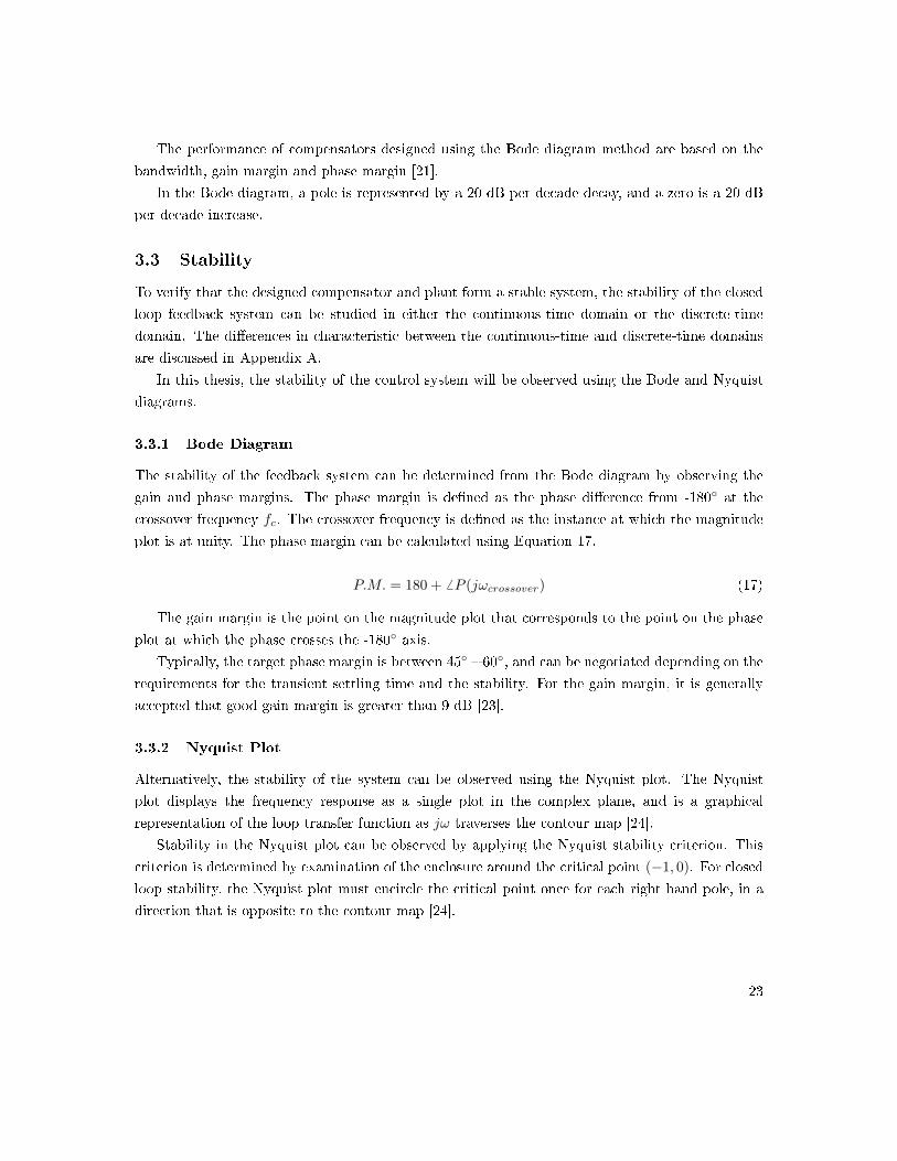
Figure 17 shows the DC voltage gain characteristic of the prototype model when operated above
the resonant frequency. From these results, it is evident that for light loading conditions, the LLC
resonant converter begins to display non-linear characteristics, which suggests a separate control
loop may be necessary for light load operation. For loading conditions approaching the nominal
load, it appears that the prototype model follows the theoretical DC gain characteristics as given
by Figure 4b. Figure 17 also shows that the boundary condition between nominal and light loading
conditions for this particular converter lies around 2.3 A.
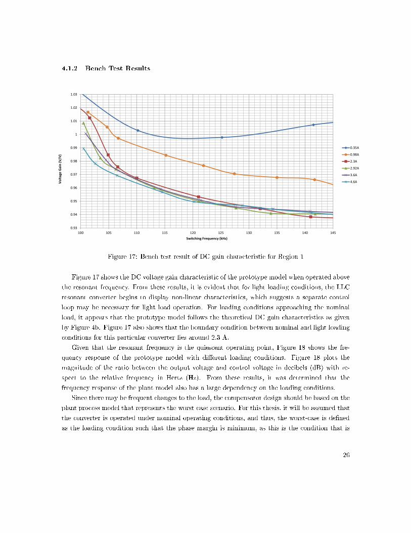
Given that the resonant frequency is the quiescent operating point, Figure 18 shows the fre-
quency response of the prototype model with di�erent loading conditions. Figure 18 plots the
magnitude of the ratio between the output voltage and control voltage in decibels (dB) with re-
spect to the relative frequency in Hertz (Hz). From these results, it was determined that the
frequency response of the plant model also has a large dependency on the loading conditions.
Since there may be frequent changes to the load, the compensator design should be based on the
plant process model that represents the worst-case scenario. For this thesis, it will be assumed that
the converter is operated under nominal operating conditions, and thus, the worst-case is de�ned
as the loading condition such that the phase margin is minimum, as this is the condition that is
26
-60
-55
-50
-45
-40
-35
-30
-25
-20
-15
-10M
ag
nitu
de
(d
B)
102
103
104
-180
-90
0
90
180
Ph
ase
(d
eg
)Bode Diagram
Frequency (Hz)
1 A
2.3 A
3 A
3.6 A
4.6 A
Figure 18: Plot of relative frequency response of prototype model under di�erent loading conditions
most likely to be overcome by problems of instability. In Figure 18, this scenario is represented by
the curve `4.6 A.'
It can be noted that the frequency response generally follows the form of a low-pass �lter (LPF),
with the addition of a high frequency pole-zero combination. Because this system appears to be
greater than second order, design of the compensator using the Bode diagram technique is preferred
over other design methods.
4.1.3 Compensator Design Results
MATLAB R© has several useful tools for digital controller development. Firstly, built-in functions
such as `c2d ' make it straightforward to convert continuous-time s-domain models to discrete-time
z-domain models. Secondly, the Control System Toolbox features the SISO Design Tool which
27
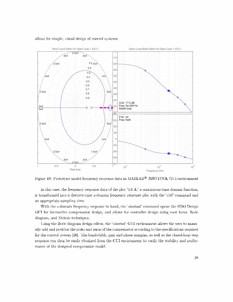
allows for simple, visual design of control systems.
102
103
104
-180
-135
-90
-45
0
45
90
135
180P.M.: InfFreq: NaN
Frequency (Hz)
Ph
ase
(d
eg
)
-60
-55
-50
-45
-40
-35
-30
-25
-20
-15
-10
G.M.: 77.5 dBFreq: 5e+004 HzStable loop
Open-Loop Bode Editor for Open Loop 1 (OL1)
Ma
gn
itu
de
(d
B)
-1 -0.5 0 0.5 1-1
-0.8
-0.6
-0.4
-0.2
0
0.2
0.4
0.6
0.8
1
5e3
1e4
1.5e4
2e42.5e4
3e4
3.5e4
4e4
4.5e4
5e4
5e3
1e4
1.5e4
2e42.5e4
3e4
3.5e4
4e4
4.5e4
5e4
0.1
0.2
0.3
0.4
0.5
0.6
0.7
0.8
0.9
Root Locus Editor for Open Loop 1 (OL1)
Real Axis
Ima
g A
xis
Figure 19: Prototype model frequency response data in MATLAB R© SISOTOOL GUI environment
In this case, the frequency response data of the plot `4.6 A,' a continuous-time domain function,
is transformed into a discrete-time z-domain frequency response plot with the `c2d ' command and
an appropriate sampling time.
With the z-domain frequency response in hand, the `sisotool ' command opens the SISO Design
GUI for interactive compensator design, and allows for controller design using root locus, Bode
diagram, and Nichols techniques.
Using the Bode diagram design editor, the `sisotool ' GUI environment allows the user to manu-
ally add and position the poles and zeros of the compensator according to the speci�cations required
for the control system [26]. The bandwidth, gain and phase margins, as well as the closed-loop step
response can then be easily obtained from the GUI environment to verify the stability and perfor-
mance of the designed compensator model.
28
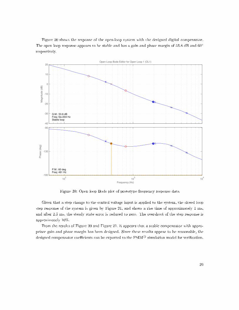
Figure 20 shows the response of the open-loop system with the designed digital compensator.
The open loop response appears to be stable and has a gain and phase margin of 53.8 dB and 60◦
respectively.
102
103
104
-180
-135
-90
P.M.: 60 degFreq: 481 Hz
Frequency (Hz)
Ph
ase
(d
eg
)
-40
-30
-20
-10
0
10
20
G.M.: 53.8 dBFreq: 5e+004 HzStable loop
Open-Loop Bode Editor for Open Loop 1 (OL1)
Ma
gn
itu
de
(d
B)
Figure 20: Open-loop Bode plot of prototype frequency response data
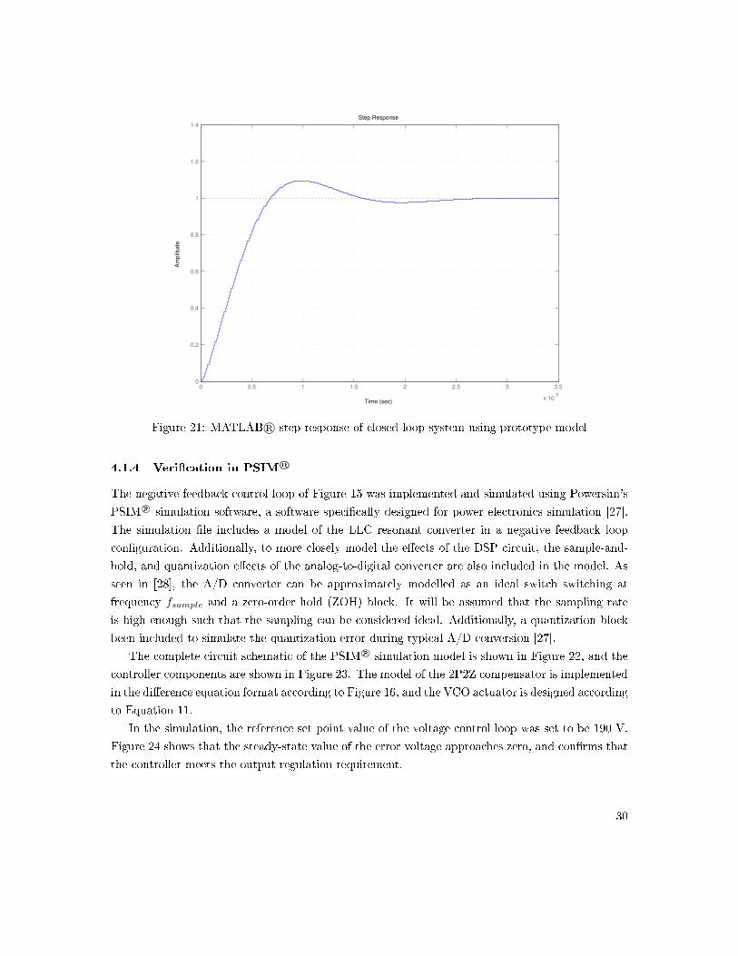
Given that a step change to the control voltage input is applied to the system, the closed-loop
step response of the system is given by Figure 21, and shows a rise time of approximately 1 ms,
and after 2.5 ms, the steady state error is reduced to zero. The overshoot of the step response is
approximately 10%.
From the results of Figure 20 and Figure 21, it appears that a stable compensator with appro-
priate gain and phase margin has been designed. Since these results appear to be reasonable, the
designed compensator coe�cients can be exported to the PSIM R© simulation model for veri�cation.
29
Step Response
Time (sec)
Am
plit
ud
e
0 0.5 1 1.5 2 2.5 3 3.5
x 10-3
0
0.2
0.4
0.6
0.8
1
1.2
1.4
Figure 21: MATLAB R© step response of closed-loop system using prototype model
4.1.4 Veri�cation in PSIM R©
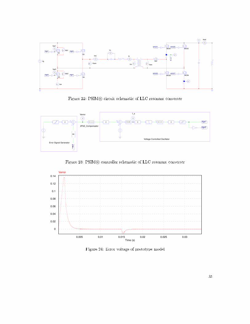
The negative feedback control loop of Figure 15 was implemented and simulated using Powersim's
PSIM R© simulation software, a software speci�cally designed for power electronics simulation [27].
The simulation �le includes a model of the LLC resonant converter in a negative feedback loop
con�guration. Additionally, to more closely model the e�ects of the DSP circuit, the sample-and-
hold, and quantization e�ects of the analog-to-digital converter are also included in the model. As
seen in [28], the A/D converter can be approximately modelled as an ideal switch switching at
frequency fsample and a zero-order hold (ZOH) block. It will be assumed that the sampling rate
is high enough such that the sampling can be considered ideal. Additionally, a quantization block
been included to simulate the quantization error during typical A/D conversion [27].
The complete circuit schematic of the PSIM R© simulation model is shown in Figure 22, and the
controller components are shown in Figure 23. The model of the 2P2Z compensator is implemented
in the di�erence equation format according to Figure 16, and the VCO actuator is designed according
to Equation 11.
In the simulation, the reference set point value of the voltage control loop was set to be 190 V.
Figure 24 shows that the steady-state value of the error voltage approaches zero, and con�rms that
the controller meets the output regulation requirement.
30
Title
Designed by
Revision Page 1 of 1
Vtank
V
Vc
A
Ip
Vm
V
Vout
Vsec
MOS1
MOS2
MOS3
MOS4
A
Isec
Vmos3
Vmos1 Vmos3
Vmos1
A
Iload
Q1
Vds1
Vds3
V
Vgs1
V
Vgs3
Vg
A
Ires
Q2 Q4
Q3
Isw
Vgs1
Vgs1
Vgs3
Vgs3
Figure 22: PSIM R© circuit schematic of LLC resonant converter
Title
Designed by
Revision Page 1 of 1
V_ref
V
Verror
K ZOH
V
f_s
K Vgs1
Vgs3
K sinr
KH(z)
2P2Z_Compensator
Voltage Controlled Oscillator
Error Signal Generator
Figure 23: PSIM R© controller schematic of LLC resonant converter
C:\Users\Brian\Documents\PSIM\LOW2HI_FINALplay.smvDate: 11:49PM 10/09/12
0
-0.5
0.5
1
1.5
2
2.5
3
Verror
0
-20
20
40
60
Imos2
0.005 0.01 0.015 0.02 0.025 0.03
Time (s)
0
0.02
0.04
0.06
0.08
0.1
0.12
0.14
Verror
Figure 24: Error voltage of prototype model
31
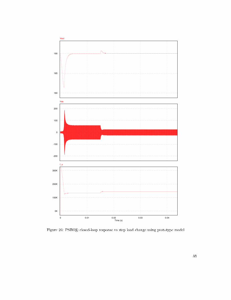
A study of the e�ects of a steady-state load step change are shown in Figure 26. A step load
change in the simulation is applied at t = 15ms, and from the results of Figure 26, it has been veri�ed
that the designed control system that has been implemented is functional and is able to maintain
output voltage regulation even when undergoing changing loading conditions. As expected, the
switching frequency fs increases when the load was decreased. Figure 26 also shows the response
of the current through the resonant tank, and the switching frequency.
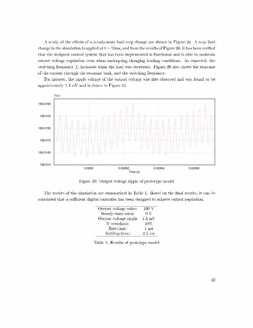
For interest, the ripple voltage of the output voltage was also observed and was found to be
approximately 1.4 mV and is shown in Figure 25.
C:\Users\Brian\Documents\PSIM\LOW2HI_FINALplay.smvDate: 11:55PM 10/09/12
0
-0.5
0.5
1
1.5
2
2.5
3
Verror
0
-20
20
40
60
Imos2
0.0295 0.02952 0.02954 0.02956
Time (s)
190.014
190.0145
190.015
190.0155
190.016
190.0165
Vout
Figure 25: Output voltage ripple of prototype model
The results of the simulation are summarized in Table 1. Based on the �nal results, it can be
concluded that a su�cient digital controller has been designed to achieve output regulation.
Output voltage value: 190 VSteady-state error: 0 V
Output voltage ripple 1.4 mV% overshoot: 10%Rise-time: 1 ms
Settling-time: 2.5 ms
Table 1: Results of prototype model
32
C:\Users\Brian\Documents\PSIM\LOW2HI_FINALplay.smvDate: 10:43PM 09/27/12
180
185
190
Vout
0
-100
-200
100
200
Ires
0 0.01 0.02 0.03 0.04
Time (s)
0K
100K
200K
300K
f_s
Figure 26: PSIM R© closed-loop response to step load change using prototype model
33

4.2 Texas Instruments R© DSP
To implement the voltage control loop digitally, a DSP is required. Texas Instruments R© (TI) has
a large portfolio of micro-controllers and digital signal processors available for use.
In this thesis, the TMS320F28035 Piccolo was selected as the ideal digital signal processor
as it has the capability to use both the on-board central processing unit (CPU) as well as the
additional Control Law AcceleratorTM (CLA) platform. The CLA has the advantage of minimizing
the processing latency of regular DSPs since it can execute time-critical control algorithms in parallel
with the main CPU [29].
The voltage control loop can be implemented onto the CLA partition of the TMS320F28035
DSP using assembly language programming. To assist with the programming related to the CLA,
the controlSUITETMpackage o�ered by TI provides many example code snippets for use.
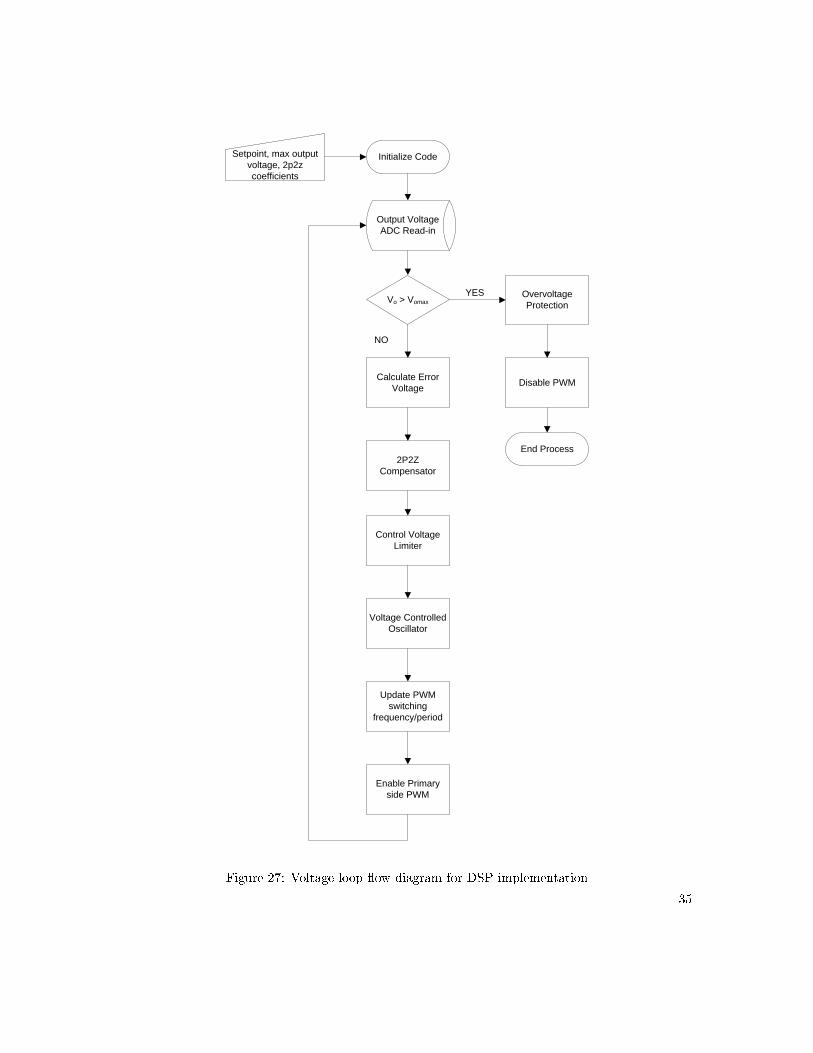
Figure 27 shows an algorithm that can be used to implement the voltage control loop with the
CLA.
34
2P2Z Digital
Compensator
Voltage Controlled
Oscillator
LLC Resonant
ConverterVoltage Divider
Voltage Setpoint Voltage Output
Vo > VomaxOvervoltage
Protection
Disable PWMCalculate Error
Voltage
2P2Z
Compensator
Voltage Controlled
Oscillator
Update PWM
switching
frequency/period
Control Voltage
Limiter
End Process
VOLTAGE LOOP MCU DESIGN FOR UPS LLC
Enable Primary
side PWM
Initialize Code
YES
NO
1) Initialize Code:
· Define voltage setpoint, max
output voltage
· Define 2p2z coefficients
· Initialize CLA processor
· Disable primary PWM
2) ADC Read:
· Read output voltage (find
average value?)
· If (Voltage Value > Vomax)
à OVP triggered and
PWM disabled.
3) Voltage Control Loop (in CLA):
· Calculate error
Verror = (Vsetpoint – Vo)
· Send error value to 2p2z
compensator
à 2p2z outputs VCTRL
· Limit VCTRL between 6V – 8V.
· Send VCTRL to VCO
àVCO outputs fswitching
4) PWM Update/Enable:
· Update bit.TBPRD in “Main”
code.
· Enable primary PWMs.
5) Restart:
· Read new output voltage
value
· Loop steps 2 – 5.
Output Voltage
ADC Read-in
Setpoint, max output
voltage, 2p2z
coefficients
Figure 27: Voltage loop �ow diagram for DSP implementation
35
5 Derivation of Control-to-Output Transfer Function
5.1 Overview
The control-to-output transfer function of the LLC resonant converter represents the ratio of the
output voltage Vo to small signal variations in the switching frequency fs. The di�culty in designing
compensators for the LLC resonant converter lies in the fact that there are few known examples in
literature of the control-to-output transfer function, which in this case represents the plant process
model of the control loop.
Modelling the small signal characteristics of the LLC resonant converter is particularly di�cult
because many averaging techniques, such as state space models cannot be used. In [7] and [30],
it is noted that unlike PWM converters, the control-to-output transfer of the converter cannot be
obtained by the state space averaging methods, due to the way energy is processed in the LLC
resonant converter.
Currently, most known applications ([30][31]) rely on bench measurements and frequency re-
sponse data to help determine the plant process model for the design of the compensation network.
In practice, the transfer function can be obtained by using a network analyzer to measure the fre-
quency response of the plant process model, and then using the data to design the compensator.
This methodology has the inherent disadvantage of requiring a pre-built functioning prototype
model.
A proposed control-to-output transfer function that does not use frequency response data was
presented in [32]. It was proposed that the control-to-output transfer function could be approxi-
mated as a third order polynomial. However, for the transfer function to be computed, variables
such as the damping factor and the beat frequency of the converter need to be known. Additionally,
a third order polynomial equation would not be able to predict the high frequency pole-zero shown
in Figure 32.
Finally, similar to the method proposed in [7], computer simulation can also be used. The
di�culty in creating a simulation model that can accurately model the true component and parasitic
models may be di�cult. With digital controllers, computer simulation is further complicated since
the modelling of the e�ects of the DSP hardware can only be approximated. Additionally, as noted
in [7], the computer simulation method requires extensive computing power.
5.2 Transfer Function Derivation
In the proceeding sections, a novel model of the small signal characteristics of the control-to-output
transfer for the LLC resonant converter will be presented. A MATLAB R© -based software program
has been developed to determine the frequency response of the derivation results, and will be
compared to the frequency response data obtained in Chapter 4.
36
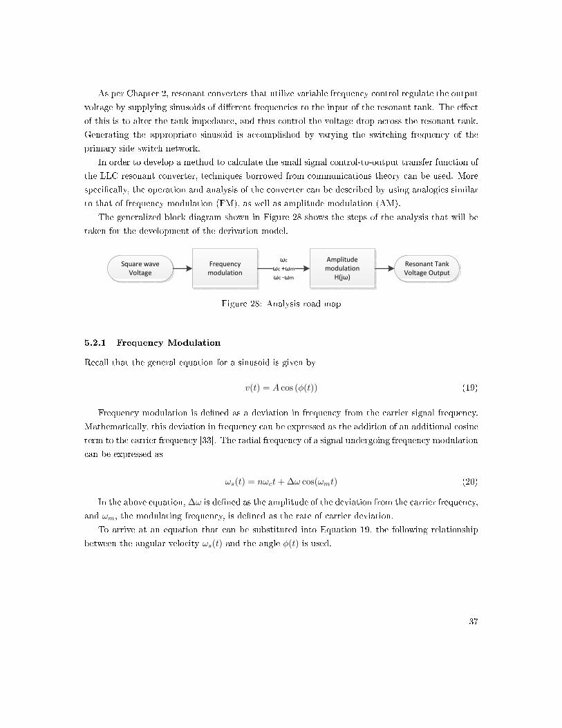
As per Chapter 2, resonant converters that utilize variable frequency control regulate the output
voltage by supplying sinusoids of di�erent frequencies to the input of the resonant tank. The e�ect
of this is to alter the tank impedance, and thus control the voltage drop across the resonant tank.
Generating the appropriate sinusoid is accomplished by varying the switching frequency of the
primary side switch network.
In order to develop a method to calculate the small signal control-to-output transfer function of
the LLC resonant converter, techniques borrowed from communications theory can be used. More
speci�cally, the operation and analysis of the converter can be described by using analogies similar
to that of frequency modulation (FM), as well as amplitude modulation (AM).
The generalized block diagram shown in Figure 28 shows the steps of the analysis that will be
taken for the development of the derivation model.
Full Bridge
Converter
Resonant Tank
H(jω)
Square
Wave
Vs(t)
Power
Transformer
V x H(jω)
V x H(j(ω+ωm))
V x H(j(ω-ωm))DC Input
Full Bridge
Rectifier with
Capacitor Filter
DC Output
Square wave
Voltage
Frequency
modulation
Amplitude
modulation
H(jω)
Resonant Tank
Voltage Output
ωc
ωc +ωm
ωc -ωm
CompensatorVoltage Controlled
Oscillator
Figure 28: Analysis road map
5.2.1 Frequency Modulation
Recall that the general equation for a sinusoid is given by
v(t) = A cos (φ(t)) (19)
Frequency modulation is de�ned as a deviation in frequency from the carrier signal frequency.
Mathematically, this deviation in frequency can be expressed as the addition of an additional cosine
term to the carrier frequency [33]. The radial frequency of a signal undergoing frequency modulation
can be expressed as
ωs(t) = nωct+ ∆ω cos(ωmt) (20)
In the above equation, ∆ω is de�ned as the amplitude of the deviation from the carrier frequency,
and ωm, the modulating frequency, is de�ned as the rate of carrier deviation.
To arrive at an equation that can be substituted into Equation 19, the following relationship
between the angular velocity ωs(t) and the angle φ(t) is used.
37
φ(t) =
∫ωs(t)dt
(21)
φ(t) = nωct+∆ω sin(ωmt)
ωm
In the scope of this thesis, it is known that the deviation is actuated by a voltage controlled
oscillator and ∆ω can be substituted by
∆ω = 2πKV COε (22)
where KV CO is the gain of the voltage controlled oscillator, and the amplitude of the applied
small signal perturbation is given by the constant ε.
Therefore, Equation 21 can be expressed as
φ(t) = 2π
(nfct+
KV COε sin(ωmt)
ωm
)(23)
To simplify Equation 23, the modulation index β can be substituted and is de�ned as
β =2πKV COε
ωm(24)
5.2.2 Square Wave Approximation
The aforementioned mathematical relationships give a description of the e�ects of frequency modu-
lation on the carrier frequency. However, prior to applying the above equations for use in analysis,
the form of the original unmodulated signal must be determined.
The aperiodic square wave waveform is supplied from a DC voltage source and is produced as
a result of switching complementary pairs of �eld e�ect transistor (FET) switches in the primary
side FET bridge. Mathematically, a generic square wave signal undergoing frequency modulation
is given as
Vs(t) =
∞∑n=1,3,5,...
4Vgnπ
sin(n2πfct+ β sin(ωmt)) (25)
In [7], it is acknowledged that analysis including harmonics up to the �fth harmonic may be
useful in modelling the control-to-output transfer function of the LLC resonant converter. Computer
simulations recorded in [7] show that by including the harmonic content, the accuracy of the models
are improved.
38
The model proposed in this thesis includes the third and �fth harmonics, in addition to the
fundamental frequency of the square wave waveform. By including the third and �fth harmonics in
the model, a more accurate understanding of the true dynamics of the converter can be observed.
Additionally, the e�ects of including supplementary sideband frequencies (for the case where |β|does not meet the condition |β| << 1) are studied and included in the new model.
Equation 25 is therefore de�ned as
Vs(t) =4Vgπ
sin (ωct+ β sin(ωmt))
+4Vg3π
sin (3ωct+ β sin(ωmt)) (26)
+4Vg5π
sin (5ωct+ β sin(ωmt))
For simplicity, each individual harmonic component is rede�ned as Vs1(t), Vs3(t), and Vs5(t).
5.2.3 Bessel Functions of the First Kind
To gain better insight to the e�ects of frequency modulation, Bessel functions are used to determine
the amplitudes of the carrier and resulting sideband frequencies.
Expanding Equation 26 by using Bessel functions has the advantage of determining the locations
of the modulated frequencies in the frequency spectrum, as well as giving the amplitude of each
frequency component. As an example, Vs1(t) can be expanded using Bessel functions and is given
by
Vs1(t) = Jo(β)4Vgπ
sin(ωct)± J1(β)4Vgπ
sin ((ωc ± ωm)t)
(27)
±J2(β)4Vgπ
sin ((ωc ± 2ωm)t)± ...± Jn(β)4Vgπ
sin ((ωc ± nωm)t)
Jn(β) is denoted as a Bessel function of the �rst kind and can be calculated by
Jn(β) =
∞∑m=0
(−1)m
m!Γ(m+ n+ 1)
(β
2
)2m+n
(28)
In Equation 28, the variable n is the nth sideband frequency, and β is the modulation index.
In lieu of Equation 28, there are existing tables developed in [34], which can be used to determine
corresponding values of Jn(β) given the value of β.
39
In [35], there is an assumption that the value of |β| is much less than one. This is normally a
useful assumption as the following simpli�cations of the Bessel functions become valid.
J0(β) ≈ 1
(29)
Jn(β) ≈ βn
n!2n
As can be seen in Equation 29, for values of β much less than one, higher order sideband
frequencies will be approximately equal to zero.
However, since the assumption that β is much less than one is not always valid, the use of
Equation 29 is quite restrictive. Therefore, in this thesis, the assumption of |β| being much less
than one is not used. Instead, the values of |β| are determined and calculated in MATLAB R© with
the function `besselj'. This function is based on the tables found in [34].
Since the |β| value is no longer assumed to be small, the higher order values of Jn(β) become
signi�cant. Therefore, the nth highest sideband to be considered remains to be determined.
It is known that the number of sidebands for the fundamental and harmonic components are
determined by the value of the modulation index β. Theoretically, under frequency modulation,
there are an in�nite number of sideband frequencies, and therefore, a �nite number of sideband
frequencies must be selected in a way such that the majority of the signal's energy is captured.
According to Equation 24, β is inversely proportional to ωm. From this, the conclusion can be
drawn that as ωm increases, the modulation index becomes small, and the total number of sideband
frequencies is reduced.
Therefore, it can be said that the "worst-case" is the scenario when ωm is at its smallest value,
such that the value of |β| becomes large. For the purpose of this thesis, the value of ωm is taken to
be located at 1000π rad/s. By setting ωm to 1000π rad/s, a corresponding value of β is determined,
and the number of sidebands required can also be determined.
To verify that there are a su�cient number of sideband frequencies, the sideband frequencies
that account for 99% of the signal energy (in the pre-determined worst case) are considered.
The energy of a carrier and sideband signals is determined by
E = Jo(β)2 +
x∑n=1
2(Jn(β))2 (30)
To determine how many sidebands are needed to have 99% of the signal energy, an increasing
number of sidebands x is added to the carrier frequency amplitude until the value of E is equal to
0.99.
It was determined that by including three pairs of symmetrical sideband frequencies to the fun-
40
damental, third and �fth harmonic components, that 99% of the signal energy would be accounted
for the case where ωm is greater than 1000π rad/s. Thus, Equation 27 can be written as
Vs1(t) = Jo(β)4Vgπ
sin(ωct)± J1(β)4Vgπ
sin ((ωc ± ωm)t)
(31)
±J2(β)4Vgπ
sin ((ωc ± 2ωm)t)± J3(β)4Vgπ
sin ((ωc ± 3ωm)t)
5.2.4 Amplitude Modulation
Each individual frequency component is then passed through and �ltered by the resonant tank
circuit at their respective frequencies. This is equivalent to amplitude modulation (AM) and is
mathematically equivalent to multiplying each frequency component with the resonant tank transfer
function at the corresponding frequency. The resulting signal represents a voltage, that will be
eventually applied to the secondary side of the converter.
As an example, the carrier, upper and lower sideband frequencies of the third harmonic under-
going amplitude modulation are given by Equations 32 - 38. Similar equations can be determined
for the fundamental and �fth harmonic components.
Vs3,carrier = J0(β)× 4Vg3π
sin(3ωct)×H(3j(ωc)) (32)
Vs3,upper1 = J1(β)× 4Vg3π
sin ((3ωc + ωm)t)×H(j(3ωc + ωm)) (33)
Vs3,lower1 = −J1(β)× 4Vg3π
sin ((3ωc − ωm)t)×H(j(3ωc − ωm)) (34)
Vs3,upper2 = J2(β)× 4Vg3π
sin ((3ωc + 2ωm)t)×H(j(3ωc + 2ωm)) (35)
Vs3,lower2 = −J2(β)× 4Vg3π
sin ((3ωc − 2ωm)t)×H(j(3ωc − 2ωm)) (36)
Vs3,upper3 = J3(β)× 4Vg3π
sin ((3ωc + 3ωm)t)×H(j(3ωc + 3ωm)) (37)
Vs3,lower3 = −J3(β)× 4Vg3π
sin ((3ωc − 3ωm)t)×H(j(3ωc − 3ωm)) (38)
41
The Euler formula is useful in this case, and is given by
sin(θ) =ejθ − e−jθ
j2(39)
Applying Equation 39 to the trigonometric term of the resonant tank outputs, the above equa-
tions can be rewritten. As an example, the equations of the carrier and sideband frequencies for
the third harmonic are shown in Equations 40 - 46. The equations for the fundamental and �fth
harmonic components can be determined similarly.
Vs3,carrier =Boe
j3ωct −B∗oe−j3ωct
j2(40)
Vs3,upper =(Bue
j3ωmt)ejωct − (Buejωmt)∗e−j3ωct
j2(41)
Vs3,lower =(Ble
−jωmt)ej3ωct − (Ble−jωmt)∗e−j3ωct
j2(42)
Vs3,upper2 =(Bu,2e
j2ωmt)ej3ωct − (Bu,2ej2ωmt)∗e−j3ωct
j2(43)
Vs3,lower2 =(Bl,2e
−j2ωmt)ej3ωct − (Bl,2e−j2ωmt)∗e−j3ωct
j2(44)
Vs3,upper3 =(Bu,3e
j3ωmt)ej3ωct − (Bu,3ej3ωmt)∗e−j3ωct
j2(45)
Vs3,lower3 =(Bl,3e
−j3ωmt)ej3ωct − (Bl,3e−j3ωmt)∗e−j3ωct
j2(46)
Where Bo, Bu, Bl, Bu,2, Bl,2, Bu,3, Bl,3 are de�ned by Equations 47 - 53
Bo = J0(β)× 4VgπH(j3ωc) (47)
Bu = J1(β)× 4Vg3π
H(j(3ωc + ωm)) (48)
Bl = −J1(β)× 4Vg3π
H(j(3ωc − ωm)) (49)
Bu,2 = J2(β)× 4Vg3π
H(j(3ωc + 2ωm)) (50)
42
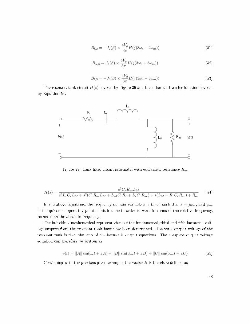
Bl,2 = −J2(β)× 4Vg3π
H(j(3ωc − 2ωm)) (51)
Bu,3 = J3(β)× 4Vg3π
H(j(3ωc + 3ωm)) (52)
Bl,3 = −J3(β)× 4Vg3π
H(j(3ωc − 3ωm)) (53)
The resonant tank circuit H(s) is given by Figure 29 and the s-domain transfer function is given
by Equation 54.
Vsquare(t)
Vo(t)
V(t)
Vsquare(t) V(t)DC
Rr Cr
Lr
LMDC Co Ro
Vo(t)Co Ro
Rac Vo(t)
z-1
z-1
z-1
z-1
+ +
+ +
u(k)e(k)b0
b1
b2
-a1
-a2
V(t)
Rr Cr
Lr
LMV(t)
Rr Cr
Rac
Lr
LM
Figure 29: Tank �lter circuit schematic with equivalent resistance Rac
H(s) =s2CrRacLM
s3LrCrLM + s2(CrRacLM + LMCrRr + LrCrRac) + s(LM +RrCrRac) +Rac(54)
In the above equations, the frequency domain variable s is taken such that s = jωm, and jωc
is the quiescent operating point. This is done in order to work in terms of the relative frequency,
rather than the absolute frequency.
The individual mathematical representations of the fundamental, third and �fth harmonic volt-
age outputs from the resonant tank have now been determined. The total output voltage of the
resonant tank is then the sum of the harmonic output equations. The complete output voltage
equation can therefore be written as
v(t) = ||A|| sin(ωct+ 6 A) + ||B|| sin(3ωct+ 6 B) + ||C|| sin(5ωct+ 6 C) (55)
Continuing with the previous given example, the vector B is therefore de�ned as
43
B = Bo +Buejωmt +Ble
−jωmt +Bu,2ej2ωmt +Bl,2e
−j2ωmt +Bu,3ej3ωmt +Bl,3e
−j3ωmt (56)
Equation 55 represents the output voltage as a sinusoid having time-varying amplitude and also
time-varying phase.
Since the goal of this analysis is to determine the change in output voltage due to the e�ect
of small variations to the switching frequency, the magnitude of Equation 55 must be evaluated.
As was discussed, the e�ect of passing frequency signals through the resonant tank is the same as
applying amplitude modulation (AM). Therefore, similar to AM analysis techniques, the envelope
of the waveform should be extracted to study the change in the output voltage [33].
From AM analysis, it is known that the magnitude of the coe�cients ||A||, ||B||, and ||C|| containthe envelope of the signal. The square of the magnitude can �rstly be determined by multiplying
the vector with its complex conjugate. E.g. for B, the magnitude can be determined by
||B||2 = BB∗ (57)
To make use of some mathematical simpli�cations, it is assumed that only the dominant DC
components are relevant. If this is true, then the following approximation can be made.
√1 + ξ ≈ 1 +
1
2ξ (58)
Thus, the magnitudes of A,B, and C are determined to be
||A|| = ||Ao||+ ||Al||
+||AoA
∗l +AuA
∗o +AlA
∗l,2 +Au,2A
∗u||
||Ao||sin(ωmt+ 6 (AoA
∗l +AuA
∗o +AlA
∗l,2 +Au,2A
∗u))
+||AoA
∗l,2 +AuA
∗l +AlA
∗l,3 +Au,2A
∗o +Au,3A
∗u||
||Ao||sin(3ωmt+ 6 (AoA
∗l,2+AuA
∗l +AlA
∗l,3+Au,2A
∗o+Au,3A
∗u))
+||AoA
∗l,3 +AuA
∗l,2 +Au,2A
∗l +Au,3A
∗o||
||Ao||sin(5ωmt+ 6 (AoA
∗l,3 +AuA
∗l,2 +Au,2A
∗l +Au,3A
∗o)) (59)
44
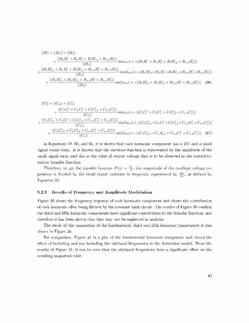
||B|| = ||Bo||+ ||Bl||
+||BoB
∗l +BuB
∗o +BlB
∗l,2 +Bu,2B
∗u||
||Bo||sin(ωmt+ 6 (BoB
∗l +BuB
∗o +BlB
∗l,2 +Bu,2B
∗u))
+||BoB
∗l,2 +BuB
∗l +BlB
∗l,3 +Bu,2B
∗o +Bu,3B
∗u||
||Bo||sin(3ωmt+ 6 (BoB
∗l,2+BuB
∗l +BlB
∗l,3+Bu,2B
∗o+Bu,3B
∗u))
+||BoB
∗l,3 +BuB
∗l,2 +Bu,2B
∗l +Bu,3B
∗o ||
||Bo||sin(5ωmt+ 6 (BoB
∗l,3 +BuB
∗l,2 +Bu,2B
∗l +Bu,3B
∗o )) (60)
||C|| = ||Co||+ ||Cl||
+||CoC
∗l + CuC
∗o + ClC
∗l,2 + Cu,2C
∗u||
||Co||sin(ωmt+ 6 (CoC
∗l + CuC
∗o + ClC
∗l,2 + Cu,2C
∗u))
+||CoC
∗l,2 + CuC
∗l + ClC
∗l,3 + Cu,2C
∗o + Cu,3C
∗u||
||Co||sin(3ωmt+ 6 (CoC
∗l,2+CuC
∗l +ClC
∗l,3+Cu,2C
∗o +Cu,3C
∗u))
+||CoC
∗l,3 + CuC
∗l,2 + Cu,2C
∗l + Cu,3C
∗o ||
||Co||sin(5ωmt+ 6 (CoC
∗l,3 + CuA
∗l,2 + Cu,2C
∗l + Cu,3C
∗o )) (61)
In Equations 59, 60, and 61, it is shown that each harmonic component has a DC and a small
signal cosine term. It is known that the envelope function is represented by the amplitude of the
small signal term, and this is the value of output voltage that is to be observed in the control-to-
output transfer function.
Therefore, to get the transfer function P (s) = Vo
f , the magnitude of the envelope voltage ex-
pression is divided by the small signal variation in frequency represented by ∆ω2π , as de�ned by
Equation 22.
5.2.5 Results of Frequency and Amplitude Modulation
Figure 30 shows the frequency response of each harmonic component and shows the contribution
of each harmonic after being �ltered by the resonant tank circuit. The results of Figure 30 con�rm
the third and �fth harmonic components have signi�cant contribution to the transfer function, and
therefore it has been shown that they may not be neglected in analysis.
The result of the summation of the fundamental, third and �fth harmonic components is also
shown in Figure 30.
For comparison, Figure 31 is a plot of the fundamental harmonic component and shows the
e�ect of including and not including the sideband frequencies in the derivation model. From the
results of Figure 31, it can be seen that the sideband frequencies have a signi�cant e�ect on the
resulting magnitude plot.
45
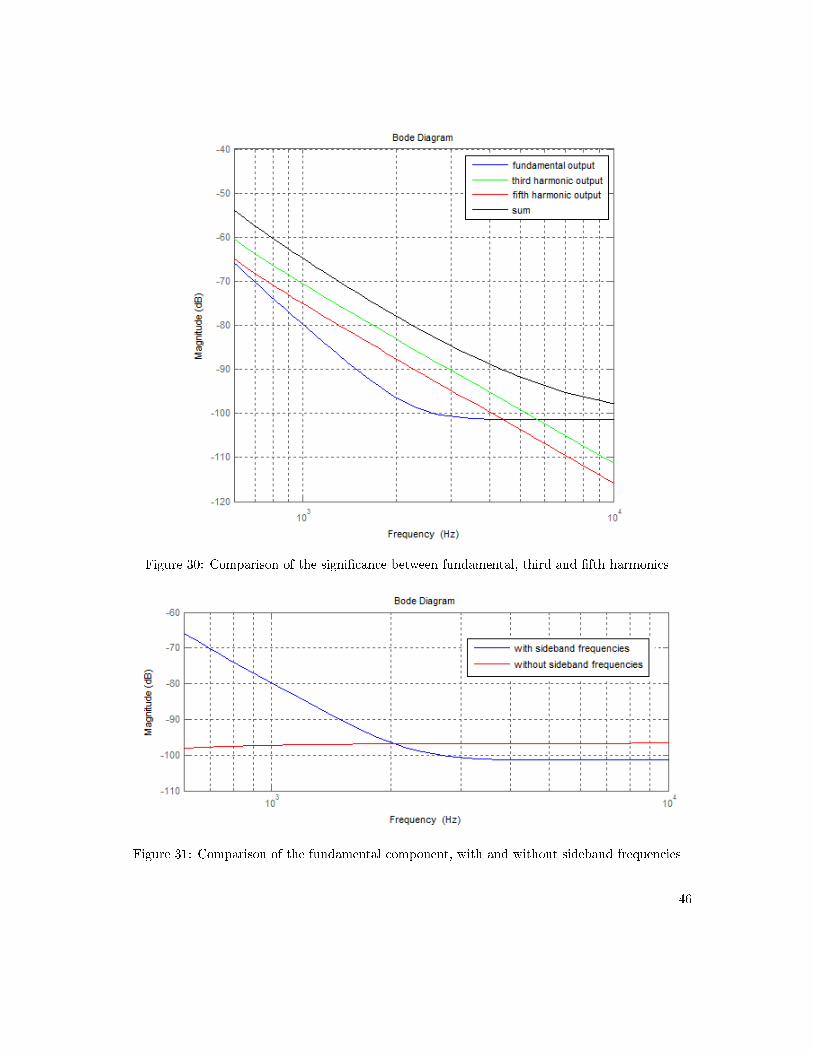
Figure 30: Comparison of the signi�cance between fundamental, third and �fth harmonics
Figure 31: Comparison of the fundamental component, with and without sideband frequencies
46
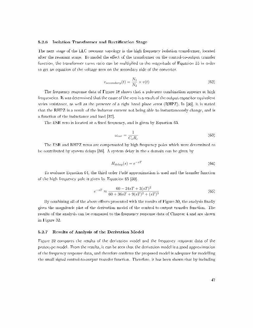
5.2.6 Isolation Transformer and Recti�cation Stage
The next stage of the LLC resonant topology is the high frequency isolation transformer, located
after the resonant stage. To model the e�ect of the transformer on the control-to-output transfer
function, the transformer turns ratio can be multiplied to the magnitude of Equation 55 in order
to get an equation of the voltage seen on the secondary side of the converter.
vsecondary(t) =N1
N2× v(t) (62)
The frequency response data of Figure 18 shows that a pole-zero combination appears at high
frequencies. It was determined that the cause of the zero is a result of the output capacitor equivalent
series resistance, as well as the presence of a right hand plane zeros (RHPZ). In [36], it is stated
that the RHPZ is a result of the inductor current not being able to instantaneously change, and is
a function of the inductance and load [37].
The ESR zero is located at a �xed frequency, and is given by Equation 63.
ωesr =1
CoRc(63)
The ESR and RHPZ zeros are compensated by high frequency poles which were determined to
be contributed by system delays [38]. A system delay in the s-domain can be given by
Hdelay(s) = e−sT (64)
To evaluate Equation 64, the third order Padé approximation is used and the transfer function
of the high frequency pole is given by Equation 65 [39].
e−sT ≈ 60− 24sT + 3(sT )2
60 + 36sT + 9(sT )2 + (sT )3(65)
By combining all of the above e�ects presented with the results of Figure 30, the analysis �nally
gives the magnitude plot of the derivation model of the control-to-output transfer function. The
results of the analysis can be compared to the frequency response data of Chapter 4 and are shown
in Figure 32.
5.2.7 Results of Analysis of the Derivation Model
Figure 32 compares the results of the derivation model and the frequency response data of the
prototype model. From the results, it can be seen that the derivation model is a good approximation
of the frequency response data, and therefore con�rms the proposed model is adequate for modelling
the small signal control-to-output transfer function. Therefore, it has been shown that by including
47
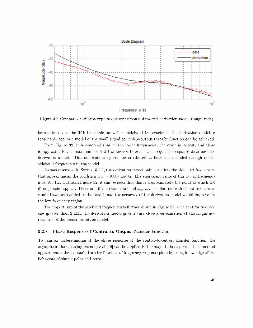
Figure 32: Comparison of prototype frequency response data and derivation model (magnitude)
harmonics up to the �fth harmonic, as well as sideband frequencies in the derivation model, a
reasonably accurate model of the small signal control-to-output transfer function can be achieved.
From Figure 32, it is observed that at the lower frequencies, the error is largest, and there
is approximately a maximum of 5 dB di�erence between the frequency response data and the
derivation model. This non-conformity can be attributed to have not included enough of the
sideband frequencies in the model.
As was discussed in Section 5.2.3, the derivation model only considers the sideband frequencies
that appear under the condition ωm = 1000π rad/s. The equivalent value of this ωm in frequency
is at 500 Hz, and from Figure 32, it can be seen that this is approximately the point at which the
discrepancies appear. Therefore, if the chosen value of ωm was smaller, more sideband frequencies
would have been added to the model, and the accuracy of the derivation model would improve for
the low frequency region.
The importance of the sideband frequencies is further shown in Figure 32, such that for frequen-
cies greater than 2 kHz, the derivation model gives a very close approximation of the magnitude
response of the bench prototype model.
5.2.8 Phase Response of Control-to-Output Transfer Function
To gain an understanding of the phase response of the control-to-output transfer function, the
asymptotic Bode tracing technique of [40] can be applied to the magnitude response. This method
approximates the s-domain transfer function of frequency response plots by using knowledge of the
behaviors of simple poles and zeros.
48
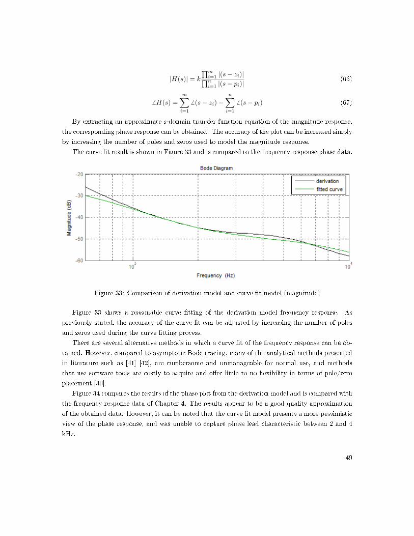
|H(s)| = k
∏mi=1 |(s− zi)|∏ni=1 |(s− pi)|
(66)
6 H(s) =
m∑i=1
6 (s− zi)−n∑i=1
6 (s− pi) (67)
By extracting an approximate s-domain transfer function equation of the magnitude response,
the corresponding phase response can be obtained. The accuracy of the plot can be increased simply
by increasing the number of poles and zeros used to model the magnitude response.
The curve �t result is shown in Figure 33 and is compared to the frequency response phase data.
Figure 33: Comparison of derivation model and curve �t model (magnitude)
Figure 33 shows a reasonable curve �tting of the derivation model frequency response. As
previously stated, the accuracy of the curve �t can be adjusted by increasing the number of poles
and zeros used during the curve �tting process.
There are several alternative methods in which a curve �t of the frequency response can be ob-
tained. However, compared to asymptotic Bode tracing, many of the analytical methods presented
in literature such as [41] [42], are cumbersome and unmanageable for normal use, and methods
that use software tools are costly to acquire and o�er little to no �exibility in terms of pole/zero
placement [30].
Figure 34 compares the results of the phase plot from the derivation model and is compared with
the frequency response data of Chapter 4. The results appear to be a good quality approximation
of the obtained data. However, it can be noted that the curve �t model presents a more pessimistic
view of the phase response, and was unable to capture phase lead characteristic between 2 and 4
kHz.
49
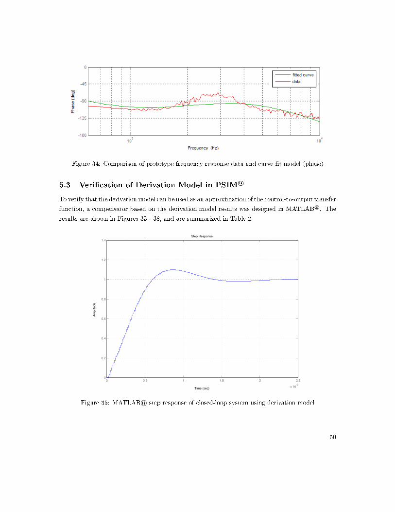
Figure 34: Comparison of prototype frequency response data and curve �t model (phase)
5.3 Veri�cation of Derivation Model in PSIM R©
To verify that the derivation model can be used as an approximation of the control-to-output transfer
function, a compensator based on the derivation model results was designed in MATLAB R©. The
results are shown in Figures 35 - 38, and are summarized in Table 2.
Step Response
Time (sec)
Am
plit
ud
e
0 0.5 1 1.5 2 2.5
x 10-3
0
0.2
0.4
0.6
0.8
1
1.2
1.4
Figure 35: MATLAB R© step response of closed-loop system using derivation model
50
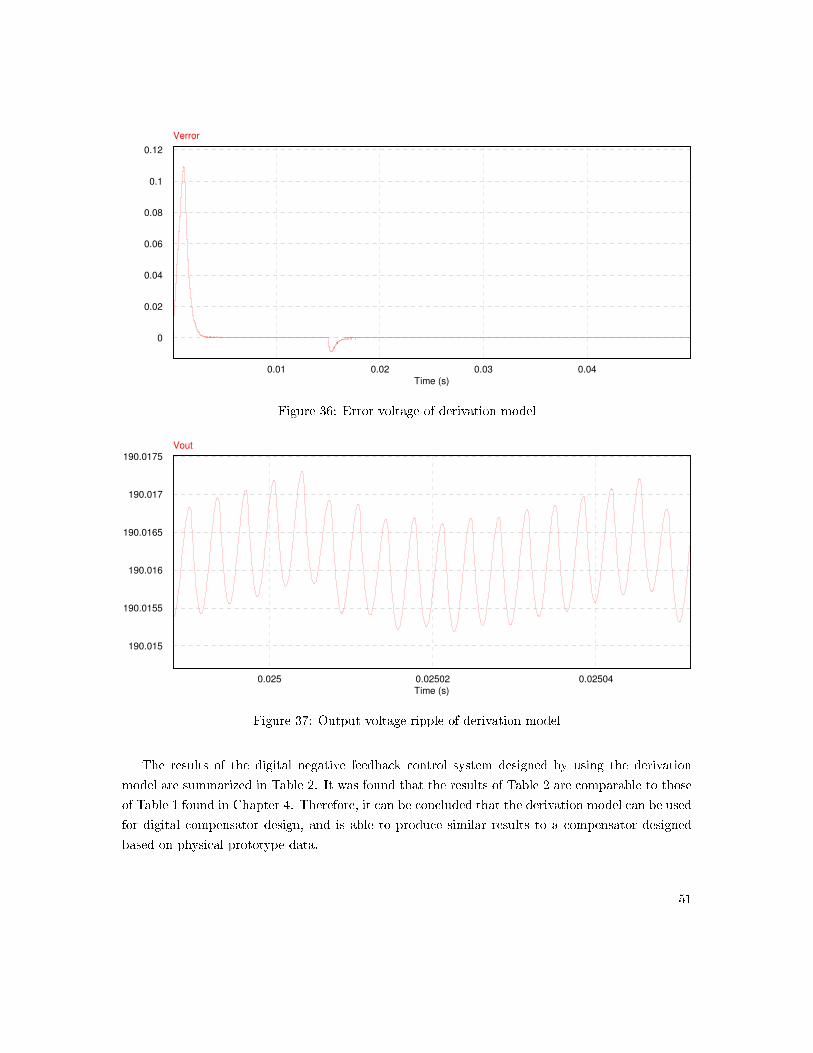
C:\Users\Brian\Documents\PSIM\LOW2HI_FINALplay.smvDate: 12:00AM 10/10/12
2
4
6
8
10
Iload
0
-100
-200
100
200
Ip
0.01 0.02 0.03 0.04
Time (s)
0
0.02
0.04
0.06
0.08
0.1
0.12
Verror
Figure 36: Error voltage of derivation model
C:\Users\Brian\Documents\PSIM\LOW2HI_FINALplay.smvDate: 12:03AM 10/10/12
2
4
6
8
10
Iload
0
-100
-200
100
200
Ip
0.025 0.02502 0.02504
Time (s)
190.015
190.0155
190.016
190.0165
190.017
190.0175Vout
Figure 37: Output voltage ripple of derivation model
The results of the digital negative feedback control system designed by using the derivation
model are summarized in Table 2. It was found that the results of Table 2 are comparable to those
of Table 1 found in Chapter 4. Therefore, it can be concluded that the derivation model can be used
for digital compensator design, and is able to produce similar results to a compensator designed
based on physical prototype data.
51
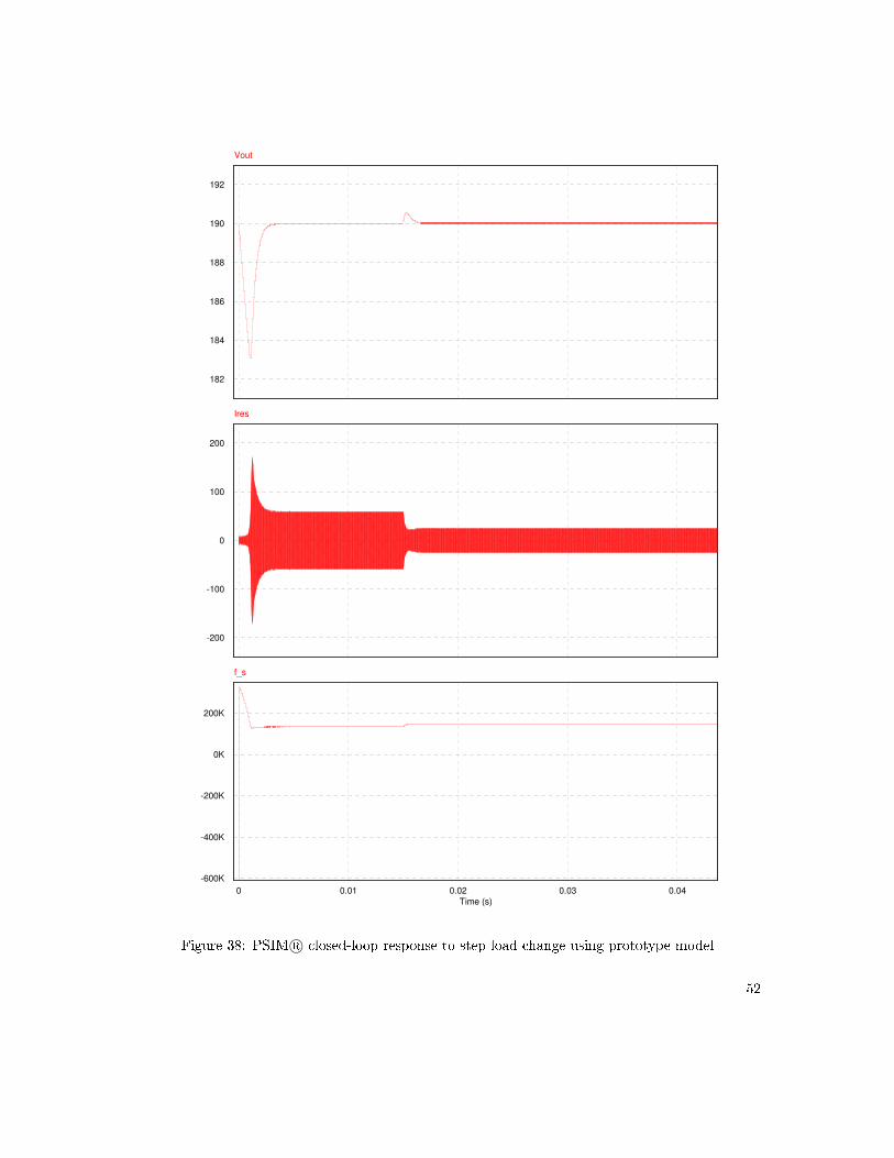
C:\Users\Brian\Documents\PSIM\LOW2HI_FINALplay.smvDate: 06:55PM 10/02/12
182
184
186
188
190
192
Vout
0
-100
-200
100
200
Ires
0 0.01 0.02 0.03 0.04
Time (s)
0K
-200K
-400K
-600K
200K
f_s
Figure 38: PSIM R© closed-loop response to step load change using prototype model
52

Output voltage value: 190 VSteady-state error: 0 V
Output voltage ripple 1.5 mV% overshoot: 10%Rise-time: 0.9 ms
Settling-time: 2 ms
Table 2: Results of derivation model
The merit of these results is the con�rmation that the small signal control-to-output transfer
function obtained by the derivation model can also be used to determine a digital compensator in
lieu of using prototype frequency response data. The �rst advantage of the derivation model method
is that only the circuit parameters of the proposed LLC resonant converter are required, and no
physical prototype model is needed to obtain the frequency response data. Secondly, compared
to computer simulation software which can also be used to obtain the plant transfer function, the
derivation model requires signi�cantly less computational power, and is considerably faster in terms
of simulation run-time.
53
6 Conclusions and Future Work
6.1 Summary
In this thesis, the LLC resonant converter topology and the variable frequency control method for
output voltage regulation was discussed in detail.
In Chapter 2, it was determined that the LLC resonant converter is an excellent choice for a
power electronic converter topology to be used in isolated DC-DC conversion applications. The
LLC resonant converter was found to feature high e�ciency, high power density, and the ability to
operate over a wide range of loading conditions. The LLC resonant converter also has many other
advantageous features including low electromagnetic interference, and soft-switching capabilities.
Chapter 3 discusses the application of a controller to the LLC resonant converter. It was
determined that the preferred control method under nominal loading conditions is variable frequency
control, a method which varies the switching frequency of the converter to regulate the output
voltage. The 2-pole-2-zero compensator was introduced as a possible suitor for a digital control
system, as it can be easily implemented within digital signal processors by using di�erence equations.
The stability of continuous and discrete-time control systems was also discussed and the application
of Bode diagrams and Nyquist plots for control system design was explored.
It was then shown in Chapter 4 that by using a combination of laboratory bench measurements,
and computer simulation, that a digital compensator could be designed to very tightly regulate the
output voltage. An algorithm was then presented to implement the voltage control loop in a digital
signal processor.
In Chapter 5, a novel derivation of the small signal control-to-output transfer function was
completed. The model includes the use of the fundamental, third and �fth harmonics, and showed
that the higher order harmonics have a signi�cant contribution to the overall transfer function, and
it should be necessary to include them to capture the true dynamics of the control-to-output transfer
function. The new model also includes higher order sideband frequencies and it was con�rmed that
the higher order sideband frequencies are required for modelling the converter for the case(s) where
the magnitude of the modulation index β does not meet the condition |β| << 1.
It was then veri�ed that the small signal control-to-output transfer function developed in the
derivation model could used to design a digital compensator for a digital negative feedback control
system. The simulation results show that an acceptable closed-loop step response and output
voltage regulation was achieved, and had comparable results to the results of Chapter 4.
Finally, it was concluded that the results of Chapter 5 were comparable to the results of Chap-
ter 4 and that the small signal control-to-output transfer function could be obtained using the
derivation model. The advantages of using the derivation model are reduced computational com-
plexity and the diminished requirement for a physical prototype model.
54
6.2 Future Work
There are several areas which can be explored further to improve the modelling of the LLC resonant
converter control-to-output transfer function.
Firstly, development of the model for the low frequency range can be investigated, and can be
achieved by decreasing the value of ωm, and therefore, introducing the case where modulation index
β is large. To calculate large values of β, a di�erent method to calculate and obtain the Bessel
function coe�cient Jn(β) may be required.
Secondly, a more in depth method to describe the recti�er model is also needed. As there
are certain loading conditions which cause the LLC resonant converter to go into discontinuous
conduction mode, the linearizion of the recti�er circuit may not be valid for all scenarios.
Thirdly, another topic of interest would be to determine a practical method in which synchronous
recti�cation can be achieved. In addition to an increase in the e�ciency of the converter, there is
also potential of having bidirectional power �ow between the input and output. In the case where
a battery is used to provide DC power at the input, this means the battery could also be charged
by the load without any additional conversion processes.
Fourthly, it was also observed that there was a signi�cant e�ect on the control-to-output transfer
function from the output capacitance and its equivalent series resistance. Therefore, a self-tuning
controller has potential to be of great value for the design of controllers for the LLC resonant
converter. It may be able to o�set errors in the modelling process that are caused by the tolerances,
the e�ects of aging capacitance, or the variation in capacitance from operation in environments with
non-ideal temperatures.
Lastly, there have also been several improvements in switching device technology since the be-
ginning of this work. Silicon carbide-based transistors and diodes have been shown many signi�cant
advantages including lower conduction losses, higher frequency operation, as well as higher operable
temperatures.
55
References
[1] D. Becker and B. Sonnenberg, �Dc microgrids in buildings and data centers,� in Telecommu-
nications Energy Conference (INTELEC), 2011 IEEE 33rd International, 2011.
[2] B. Mammano, �Resonant mode converter topologies,� pp. 1�2, 2001. Texas Instruments appli-
cation note.
[3] F. Canales, P. Barbosa, and F. C. Lee, �A wide input voltage and load output variations
�xed-frequency zvs dc/dc llc resonant converter for high-power applications,� in Industry Ap-
plications Conference, 37th IAS Annual Meeting, 2002.
[4] G. Pledl, M. Tauer, and D. Buecherl, �Theory of operation, design procedure and simulation of a
bidirectional llc resonant converter for vehicular applications,� in Vehicle Power and Propulsion
Conference (VPPC), 2010 IEEE, 2010.
[5] D. J. Tschirhart and P. K. Jain, �Digital control of resonant converters at ultra high frequency,�
in Telecommunications Energy Conference (INTELEC), 32nd International, 2010.
[6] R. W. Erickson and D. Maksimovic, Fundamentals of Power Electronics. Springer; 2nd edition,
2001.
[7] B. Yang, Topology investigation of front end DC/DC converter for distributed power system.
PhD thesis, Virginia Polytechnic Institute and State University, 2003.
[8] B. Lu, W. Liu, Y. Liang, F. C. Lee, and J. D. van Wyk, �Optimal design methodology for
llc resonant converter,� in Applied Power Electronics Conference and Exposition, 2006. APEC
'06. Twenty-First Annual IEEE, 2006.
[9] R. Locher, �Introduction to power mosfets and their applications,� p. 1, 1998.
[10] Y.-F. Liu and W. Eberle, �Recent developments in switching mode power supply technologies,�
IEEE Canadian Review, vol. 61, pp. 9�13, 2009.
[11] D. Fu, Topology Investigation and System Optimization of Resonant Converters. PhD thesis,
Virginia Polytechnic Institute and State University, 2010.
[12] H. Choi, �Analysis and design of llc resonant converter with integrated transformer,� in Applied
Power Electronics Conference, APEC 2007 - Twenty Second Annual IEEE, 2007.
[13] D. Fu, Y. Liu, F. C. Lee, and M. Xu, �A novel driving scheme for synchronous recti�ers in llc
resonant converters,� Power Electronics, IEEE Transactions on, vol. 24, pp. 1321�1329, 2009.
56
[14] D. Wang, L. Jia, Y.-F. Liu, and P. Sen, �An improved driving method for synchronous recti�er
using drain-source voltage sensing,� in Applied Power Electronics Conference and Exposition
(APEC), 2011 Twenty-Sixth Annual IEEE, 2011.
[15] Y. Liu, �High e�ciency optimization of llc resonant converter for wide load range,� Master's
thesis, Virginia Polytechnic Institute and State University, 2007.
[16] Y. Ye, C. Yan, J. Zeng, and J. Ying, �A novel light load solution for llc series resonant con-
verter,� in Telecommunications Energy Conference, 2007. INTELEC 2007. 29th International,
2007.
[17] W.-J. Lee, S.-W. Choi, C.-E. Kim, and G.-W. Moon, �A new pwm-controlled quasi-resonant
converter for a high e�ciency pdp sustaining power module,� Power Electronics, IEEE Trans-
actions on, vol. 23, pp. 1782�1790, 2008.
[18] R. Poley, �Digital control theory seminar; student manual.� Texas Instruments, 2012.
[19] G. F. Franklin, J. D. Powell, and M. L. Workman, Digital Control of Dynamic Systems.
Addison-Wesley, 1998.
[20] B. Akin and D. Chang, �Optimal digital power control using llc resonant converters,� April
2012.
[21] M. Gopal, Control Systems: Principles and Design. Tata McGraw-Hill Publishing Company,
2008.
[22] S. Engelberg, A Mathematical Introduction to Control Theory. Imperial College Press, 2005.
[23] G. F. Franklin, J. D. Powell, and A. Emami-Naeini, Feedback Control of Dynamic Systems.
Addison-Wesley Long Man Publishing Co., 1993.
[24] R. Poley, �Control theory seminar; student manual.� Texas Instruments, 2012.
[25] S. M. Shinners, Modern Control System Theory and Design. John Wiley & Sons, 1998.
[26] MATLAB, version 7.11.0.584 (R2010b). Natick, Massachusetts: The MathWorks Inc., 2010.
[27] Powersim, PSIM User Manual. www.powersimtech.com.
[28] N. Macia, Modeling and Control of Dynamic Systems. Thomson Delmar Learning, 2005.
[29] S. Chon, �What it takes to do e�cient and cost-e�ective real-time control with a single micro-
controller: The c2000 advantage,� p. 3, January 2011.
57
[30] P. Spanik, P. Drgona, and M. Frivaldsky, �Simulation based method for mathematical model
design of llc power converter,�
[31] H. Huang, �Feedback loop design of an llc resonant power converter,� Texas Insturments Ap-
plication Report, 2010.
[32] J. Jang, M. Joung, S. Choi, Y. Choi, and B. Choi, �Current mode control for llc series resonant
dc-to-tc converters,� in Applied Power Electronics Conference and Exposition (APEC), 2011
Twenty-Sixth Annual IEEE, 2011.
[33] T. G. Thomas and S. C. Sekhar, Communication Theory. Tata McGraw-Hill Publishing Com-
pany, 2006.
[34] M. Abramowitz and I. A. Stegun, Handbook of Mathematical Functions With Formulas,
Graphs, and Mathematical Tables. National Burea of Standards Applied Mathematics Series,
December 1972.
[35] R. W. Erickson, �Fm/am modeling of the envelope transfer function.� ECEN 5817 course notes.
[36] C. P. Basso, Switch-Mode Power Supply SPICE Cookbook. McGraw-Hill Prof Med/Tech, 2001.
[37] R. Zaitsu, �Voltage mode boost converter small signal control loop analysis using the tps61030,�
Texas Instruments Application Report, pp. 2�8, 2009.
[38] R. Petkov and G. Anguelov, �Current mode control of frequency controlled resonant convert-
ers,� in Telecommunications Energy Conference, 1998. INTELEC. Twentieth International,
1998.
[39] M.Vajta, �Some remarks on pade approximations,� in 3rd TEMPUS-INTCOM Symposium,
2000.
[40] J. Marti, �Wave propagation in frequency dependent lines: The fd-line model,� 2004. EECE
560 course notes.
[41] W. S. Cleveland, S. J. Devlin, and E. Grosse, �Regression by local �tting: Methods, properties,
and computational algorithms,� Journal Of Econometrics, vol. 37, pp. 87�114, 1988.
[42] G. Ferreres and J. Biannic, �Frequency domain curve �tting: a generalized approach,� tech.
rep., ONERA/DCSD: Systems Control and Flight Dynamics Department, 2001.
58

Appendices
Appendix A: Observation of Stability in Continuous and Discrete-time
domains
A1: Continuous-time domain
To determine the stability and the dynamic characteristics of the closed loop feedback system of
Figure 14, the transfer function of Figure 14 can be described by Equation A-1. Assuming that the
actuator has a gain equal to 1,
T (s) =G(s)P (s)
1 +G(s)P (s)(A-1)
In the continuous-time domain, the stability of the feedback system is observed on the s-domain
plane. The stability can be determined by evaluating the denominator of Equation A-1, also known
as the characteristic equation. Solving for the roots of the characteristic equation gives the poles
of the system, which are indicators of the system's stability.
A system that contains only poles on the left hand side of the jω axis of the s-domain plane are
considered to be stable, while systems with poles on the right hand side of the jω axis are unstable.
Marginally stable systems have poles on the jω axis.
59

A2: Discrete-time domain
In the discrete-time domain, the stability of the feedback system is observed with respect to the
z-domain unit circle. Stable systems have all poles located inside of the unit circle, while unstable
systems have poles located outside of the unit circle. Finally, marginally stable systems have poles
located on the unit circle.
Figure A-1: Unit circle in the z-domain
60
Appendix B: PSIM R©simulation schematics
Title
Designed by
Revision Page 1 of 1
Vtank
V
Vc
A
Ip
Vm
V
Vout
Vsec
MOS1
MOS2
MOS3
MOS4
A
Isec
Vmos3
Vmos1 Vmos3
Vmos1
A
Iload
Imos3
Imos1V
Vmos1
V
Vmos3
Q1
Vds1
Vds3
V
Vgs1
V
Vgs3
A
Ires
Q2 Q4
Q3
Isw
Vgs1
Vgs1
Vgs3
Vgs3
Vout
V
Vout_digital
V_ref
V
Verror
K ZOH
V
f_s
K Vgs1
Vgs3
K
ZOH
Vmos1
Vmos3
VctrlError sinr
K
V
Figure B-1: PSIM R© closed loop circuit schematic of LLC resonant converter
Title
Designed by
Revision Page 1 of 1
Vtank
V
V_Cr
V
Vout
A
Isec
A
Iload
Q1
Vds1
Vds3
V
Vgs1
V
Vgs3
Vin
A
I_r
Q2 Q4
Q3
Isw
Vgs1
Vgs1
Vgs3
Vgs3
K ZOH
V
f
K Vgs1
Vgs3
sinr
K
A
I_o
A
Ip
Vm
I_LM
Figure B-2: PSIM R© open loop circuit schematic of LLC resonant converter
61
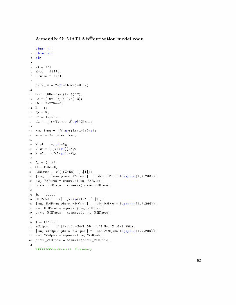
Appendix C: MATLAB R©derivation model code
1 c l e a r a l l
2 c l o s e a l l
3 c l c
4
5 Vg = 48 ;
6 Kvco = 32779;
7 Trat io = 15/4 ;
8
9 delta_w = 2∗ pi ∗(Kvco ) ∗0 . 0 2 ;10
11 Lm = (80 e−6) ∗ ( (4/15) ^2) ;12 Lr = (10 e−6) /( (15/4) ^2) ;
13 Cr = 9∗270e−9;
14 R = 1 ;
15 Rr = R;
16 Ro = 170/4 . 6 ;
17 Rac = ((8∗ Trat io ^2)/ p i ^2)∗Ro ;18
19 r e s_freq = 1/( sq r t ( Lr∗Cr) ∗2∗ pi )20 w_so = 2∗ pi ∗ r e s_freq ;
21
22 V_s1 = (4/ p i ) ∗Vg ;23 V_s3 = (4/(3∗ pi ) ) ∗Vg ;24 V_s5 = (4/(5∗ pi ) ) ∗Vg ;25
26 Rc = 0 . 1 5 9 ;
27 C = 470e−6;
28 ESRzero = t f ( [ (C∗Rc) 1 ] , [ 1 ] ) ;
29 [ mag_ESRzero phase_ESRzero ] = bode (ESRzero , l og space (1 , 6 , 200 ) ) ;
30 mag_ESRzero = squeeze (mag_ESRzero) ;
31 phase_ESRzero = squeeze ( phase_ESRzero ) ;
32
33 f z = 3100 ;
34 RHPzero = t f ([−1/(2∗ pi ∗ f z ) 1 ] , [ 1 ] ) ;
35 [mag_RHPzero phase_RHPzero ] = bode (RHPzero , l og space (1 , 6 , 200 ) ) ;
36 mag_RHPzero = squeeze (mag_RHPzero) ;
37 phase_RHPzero = squeeze ( phase_RHPzero ) ;
38
39 T = 1/8000;
40 ZOHpole = t f ( [ 3∗T^2 −24∗T 60 ] , [T^3 9∗T^2 36∗T 60 ] ) ;
41 [ mag_ZOHpole phase_ZOHpole ] = bode (ZOHpole , l og space (1 ,6 , 200) ) ;
42 mag_ZOHpole = squeeze (mag_ZOHpole) ;
43 phase_ZOHpole = squeeze ( phase_ZOHpole ) ;
44
45 %%%%%%%%fundamental f requency
62

46 a = Cr∗Rac∗Lm;
47 b = Lr∗Cr∗Lm;
48 c = (Cr∗Rac∗Lm)+(Lm∗Cr∗Rr)+(Lr∗Cr∗Rac) ;49 d = Lm+(Rr∗Cr∗Rac) ;50 e = Rac ;
51
52 %with Rload
53 H_jwso = t f ( [ a ∗( i ∗w_so) ^2 ] , [ b∗( i ∗w_so)^3+c ∗( i ∗w_so)^2+d∗( i ∗w_so)+e ] ) ;54 H_jwsoConj = t f ( [ a∗(− i ∗w_so) ^2 ] , [ b∗(− i ∗w_so)^3+c∗(− i ∗w_so)^2+d∗(− i ∗w_so)+e ] ) ;55
56 %with Rload
57 H_jwsoPluswm = t f ( [ a a∗2∗ i ∗w_so −a∗w_so^2 ] , [ b (b∗3∗ i ∗w_so+c ) (−b∗3∗w_so^2+c ∗2∗ i ∗w_so+d) ( e−c∗w_so^2−b∗ i ∗w_so^3+d∗ i ∗w_so) ] ) ;
58 H_jwsoPluswmConj = t f ( [ a a∗2∗ i ∗w_so −a∗w_so^2] , [−b (−b∗3∗ i ∗w_so+c ) (b∗3∗w_so^2+c ∗2∗ i∗w_so−d) (b∗ i ∗w_so^3−c∗w_so^2−d∗ i ∗w_so+e ) ] ) ;
59
60 %with Rload
61 H_jwsoMinuswm = t f ( [ a −2∗ i ∗w_so∗a −a∗w_so^2] , [−b (b∗3∗ i ∗w_so+c ) (b∗3∗w_so^2−c ∗2∗ i ∗w_so−d) ( e−b∗ j ∗w_so^3−c∗w_so^2+d∗ i ∗w_so) ] ) ;
62 H_jwsoMinuswmConj = t f ( [ a −2∗ i ∗w_so∗a −a∗w_so^2 ] , [ b (−b∗3∗ i ∗w_so+c ) (−b∗3∗w_so^2−c
∗2∗ i ∗w_so+d) ( e−c∗w_so^2+b∗ i ∗w_so^3−d∗ i ∗w_so) ] ) ;63
64 %with Rload
65 H_jwsoPlus2wm = t f ( [ 4∗ a 4∗a∗ i ∗w_so −a∗w_so^2 ] , [ 8∗b (12∗b∗ i ∗w_so+4∗c ) (−b∗6∗w_so^2+4∗i ∗c∗w_so+2∗d) ( e+d∗ i ∗w_so−b∗ i ∗w_so^3−c∗w_so^2) ] ) ;
66 H_jwsoPlus2wmConj = t f ( [ 4∗ a 4∗a∗ i ∗w_so −a∗w_so^2] , [−8∗b (−12∗b∗ i ∗w_so+4∗c ) (b∗6∗w_so^2+4∗ i ∗w_so∗c−2∗d) (b∗ i ∗w_so^3−c∗w_so^2−d∗ i ∗w_so+e ) ] ) ;
67
68 %with Rload
69 H_jwsoMinus2wm = t f ( [ 4∗ a −4∗a∗ i ∗w_so −a∗w_so^2] , [−8∗b (12∗b∗ i ∗w_so+4∗c ) (6∗b∗w_so^2−4∗c∗ i ∗w_so−2∗d) ( e+d∗ i ∗w_so−b∗ j ∗w_so^3−c∗w_so^2) ] ) ;
70 H_jwsoMinus2wmConj = t f ( [ 4∗ a −4∗a∗ i ∗w_so −a∗w_so^2 ] , [ 8∗b (−12∗b∗ i ∗w_so+4∗c ) (−6∗b∗w_so^2−4∗c∗ i ∗w_so+2∗d) ( e−i ∗d∗w_so−c∗w_so^2+b∗ i ∗w_so^3) ] ) ;
71
72 %wth Rload
73 H_jwsoPlus3wm = t f ( [ 9∗ a 6∗a∗ i ∗w_so −a∗w_so^2 ] , [ 27∗b (27∗b∗ i ∗w_so+9∗c ) (−9∗b∗w_so^2+6∗c∗ i ∗w_so+3∗d) ( e+d∗ i ∗w_so−c∗w_so^2−b∗ i ∗w_so^3) ] ) ;
74 H_jwsoPlus3wmConj = t f ( [ 9∗ a 6∗a∗ i ∗w_so −a∗w_so^2] , [−27∗b (−27∗b∗ i ∗w_so+9∗c ) (9∗b∗w_so^2+6∗c∗ i ∗w_so−3∗d) ( e−i ∗d∗w_so−c∗w_so^2+b∗ i ∗w_so^3) ] ) ;
75
76 %with Rload
77 H_jwsoMinus3wm = t f ( [ 9∗ a −6∗a∗ i ∗w_so −a∗w_so^2] , [−27∗b (27∗b∗ i ∗w_so+9∗c ) (9∗b∗w_so^2−6∗c∗ i ∗w_so−3∗d) ( e+d∗ i ∗w_so−c∗w_so^2−b∗ i ∗w_so^3) ] ) ;
78 H_jwsoMinus3wmConj = t f ( [ 9∗ a −6∗a∗ i ∗w_so −a∗w_so^2 ] , [ 27∗b (−27∗b∗ i ∗w_so+9∗c ) (−9∗b∗w_so^2−6∗c∗ i ∗w_so+3∗d) ( e−d∗ i ∗w_so−c∗w_so^2+b∗ i ∗w_so^3) ] ) ;
79
80 beta = t f ( [ delta_w ] , [−1∗ i 0 ] ) ;
63
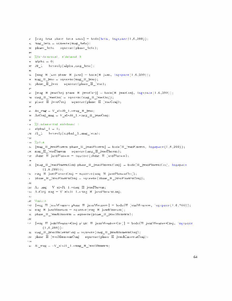
81 [ mag_beta phase_beta wout ] = bode ( beta , l og space (1 , 6 , 200 ) ) ;
82 mag_beta = squeeze (mag_beta ) ;
83 phase_beta = squeeze ( phase_beta ) ;
84
85 %fundamental , s ideband 0
86 alpha = 0 ;
87 J0_1 =b e s s e l j ( alpha , mag_beta ) ;
88
89 [mag_H_jwso phase_H_jwso ] = bode (H_jwso , l og space (1 , 6 , 200 ) ) ;
90 mag_H_jwso = squeeze (mag_H_jwso) ;
91 phase_H_jwso = squeeze (phase_H_jwso ) ;
92
93 [ mag_H_jwsoConj phase_H_jwsoConj ] = bode (H_jwsoConj , l og space (1 , 6 , 200 ) ) ;
94 mag_H_jwsoConj = squeeze (mag_H_jwsoConj) ;
95 phase_H_jwsoConj = squeeze ( phase_H_jwsoConj ) ;
96
97 Ao_mag = V_s1∗J0_1 .∗mag_H_jwso ;
98 AoConj_mag = V_s1∗J0_1 .∗mag_H_jwsoConj ;
99
100 %fundamental s ideband 1
101 alpha1_1 = 1 ;
102 J1_1 =b e s s e l j ( alpha1_1 , mag_beta ) ;
103
104 %plus
105 [mag_H_jwsoPluswm phase_H_jwsoPluswm ] = bode (H_jwsoPluswm , log space (1 , 6 , 200) ) ;
106 mag_H_jwsoPluswm = squeeze (mag_H_jwsoPluswm) ;
107 phase_H_jwsoPluswm = squeeze (phase_H_jwsoPluswm) ;
108
109 [ mag_H_jwsoPluswmConj phase_H_jwsoPluswmConj ] = bode (H_jwsoPluswmConj , l og space
(1 , 6 , 200 ) ) ;
110 mag_H_jwsoPluswmConj = squeeze (mag_H_jwsoPluswmConj) ;
111 phase_H_jwsoPluswmConj = squeeze ( phase_H_jwsoPluswmConj ) ;
112
113 Au_mag = V_s1∗J1_1 .∗mag_H_jwsoPluswm ;
114 AuConj_mag = V_s1∗J1_1 .∗mag_H_jwsoPluswmConj ;
115
116 %minus
117 [mag_H_jwsoMinuswm phase_H_jwsoMinuswm ] = bode (H_jwsoMinuswm , log space (1 , 6 , 200 ) ) ;
118 mag_H_jwsoMinuswm = squeeze (mag_H_jwsoMinuswm) ;
119 phase_H_jwsoMinuswm = squeeze (phase_H_jwsoMinuswm) ;
120
121 [ mag_H_jwsoMinuswmConj phase_H_jwsoMinuswmConj ] = bode (H_jwsoMinuswmConj , l og space
(1 , 6 , 200 ) ) ;
122 mag_H_jwsoMinuswmConj = squeeze (mag_H_jwsoMinuswmConj) ;
123 phase_H_jwsoMinuswmConj = squeeze (phase_H_jwsoMinuswmConj ) ;
124
125 Al_mag = −V_s1∗J1_1 .∗mag_H_jwsoMinuswm ;
64

126 AlConj_mag = −V_s1∗J1_1 .∗mag_H_jwsoMinuswmConj ;
127
128 %fundamental , s ideband 2
129 alpha2 = 2 ;
130 J2_1 =b e s s e l j ( alpha2 , mag_beta ) ;
131
132 %plus2wm
133 [ mag_H_jwsoPlus2wm phase_H_jwsoPlus2wm ] = bode (H_jwsoPlus2wm , log space (1 , 6 , 200 ) ) ;
134 mag_H_jwsoPlus2wm = squeeze (mag_H_jwsoPlus2wm) ;
135 phase_H_jwsoPlus2wm = squeeze (phase_H_jwsoPlus2wm) ;
136
137 [ mag_H_jwsoPlus2wmConj phase_H_jwsoPlus2wmConj ] = bode (H_jwsoPlus2wmConj , l og space
(1 , 6 , 200 ) ) ;
138 mag_H_jwsoPlus2wmConj = squeeze (mag_H_jwsoPlus2wmConj ) ;
139 phase_H_jwsoPlus2wmConj = squeeze ( phase_H_jwsoPlus2wmConj ) ;
140
141 Au2_mag = V_s1∗J2_1 .∗mag_H_jwsoPlus2wm ;
142 Au2Conj_mag = V_s1∗J2_1 .∗mag_H_jwsoPlus2wmConj ;
143
144 %minus2wm
145 [mag_H_jwsoMinus2wm phase_H_jwsoMinus2wm ] = bode (H_jwsoMinus2wm , log space (1 ,6 , 200) ) ;
146 mag_H_jwsoMinus2wm = squeeze (mag_H_jwsoMinus2wm) ;
147 phase_H_jwsoMinus2wm = squeeze (phase_H_jwsoMinus2wm) ;
148
149 [ mag_H_jwsoMinus2wmConj phase_H_jwsoMinus2wmConj ] = bode (H_jwsoMinus2wmConj ,
l og space (1 , 6 , 200 ) ) ;
150 mag_H_jwsoMinus2wmConj = squeeze (mag_H_jwsoMinus2wmConj) ;
151 phase_H_jwsoMinus2wmConj = squeeze (phase_H_jwsoMinus2wmConj ) ;
152
153 Al2_mag = V_s1∗J2_1 .∗mag_H_jwsoMinus2wm ;
154 Al2Conj_mag = V_s1∗J2_1 .∗mag_H_jwsoMinus2wmConj ;
155
156 %fundamental , s ideband3
157 alpha3 = 3 ;
158 J3_1 =b e s s e l j ( alpha3 , mag_beta ) ;
159
160 %plus3wm
161 [ mag_H_jwsoPlus3wm phase_H_jwsoPlus3wm ] = bode (H_jwsoPlus3wm , log space (1 , 6 , 200 ) ) ;
162 mag_H_jwsoPlus3wm = squeeze (mag_H_jwsoPlus3wm) ;
163 phase_H_jwsoPlus3wm = squeeze (phase_H_jwsoPlus3wm) ;
164
165 [ mag_H_jwsoPlus3wmConj phase_H_jwsoPlus3wmConj ] = bode (H_jwsoPlus3wmConj , l og space
(1 , 6 , 200 ) ) ;
166 mag_H_jwsoPlus3wmConj = squeeze (mag_H_jwsoPlus3wmConj ) ;
167 phase_H_jwsoPlus3wmConj = squeeze ( phase_H_jwsoPlus3wmConj ) ;
168
169 Au3_mag = V_s1∗J3_1 .∗mag_H_jwsoPlus3wm ;
65

170 Au3Conj_mag = V_s1∗J3_1 .∗mag_H_jwsoPlus3wmConj ;
171
172 %minus3wm
173 [mag_H_jwsoMinus3wm phase_H_jwsoMinus3wm ] = bode (H_jwsoMinus3wm , log space (1 ,6 , 200) ) ;
174 mag_H_jwsoMinus3wm = squeeze (mag_H_jwsoMinus3wm) ;
175 phase_H_jwsoMinus3wm = squeeze (phase_H_jwsoMinus3wm) ;
176
177 [ mag_H_jwsoMinus3wmConj phase_H_jwsoMinus3wmConj ] = bode (H_jwsoMinus3wmConj ,
l og space (1 , 6 , 200 ) ) ;
178 mag_H_jwsoMinus3wmConj = squeeze (mag_H_jwsoMinus3wmConj) ;
179 phase_H_jwsoMinus3wmConj = squeeze (phase_H_jwsoMinus3wmConj ) ;
180
181 Al3_mag = V_s1∗J3_1 .∗mag_H_jwsoMinus3wm ;
182 Al3Conj_mag = V_s1∗J3_1 .∗mag_H_jwsoMinus3wmConj ;
183
184 a1 = (Ao_mag.∗AlConj_mag)+(Au_mag.∗AoConj_mag)+(Al_mag .∗Al2Conj_mag)+(Au2_mag.∗AuConj_mag) ;
185 a2 = (Ao_mag.∗Al2Conj_mag)+(Au_mag.∗AlConj_mag)+(Al_mag .∗Al3Conj_mag)+(Au2_mag.∗AoConj_mag)+(Au3_mag.∗AuConj_mag) ;
186 a3 = (Ao_mag.∗Al3Conj_mag)+(Au_mag.∗Al2Conj_mag)+(Au2_mag.∗AlConj_mag)+(Au3_mag.∗AoConj_mag) ;
187
188 fundamentalOutput = ( sq r t ( (1/3 ) ∗( a1 .^2+a2.^2+a3 .^2) ) ) . / (Ao_mag) ;
189 fundamentalOutput = ((1/ delta_w ) ∗ fundamentalOutput ) ;
190
191 %%%%%%%%th i rd harmonic
192
193 %with Rload
194 H_3jwso = t f ( [ a ∗(3∗ i ∗w_so) ^2 ] , [ b∗(3∗ i ∗w_so)^3+c ∗(3∗ i ∗w_so)^2+d∗(3∗ i ∗w_so)+e ] ) ;195 H_3jwsoConj = t f ( [ a∗(−3∗ i ∗w_so) ^2 ] , [ b∗(−3∗ i ∗w_so)^3+c∗(−3∗ i ∗w_so)^2+d∗(−3∗ i ∗w_so)+e
] ) ;
196
197 %with Rload
198 H_3jwsoPluswm = t f ( [ a a∗6∗ i ∗w_so −a∗9∗w_so^2 ] , [ b (b∗9∗ i ∗w_so+c ) (−b∗27∗w_so^2+c ∗6∗ i ∗w_so+d) ( e−9∗c∗w_so^2−27∗b∗ i ∗w_so^3+3∗d∗ i ∗w_so) ] ) ;
199 H_3jwsoPluswmConj = t f ( [ a a∗6∗ i ∗w_so −a∗9∗w_so^2] , [−b (−b∗9∗ i ∗w_so+c ) (b∗27∗w_so^2+c
∗6∗ i ∗w_so−d) (27∗b∗ i ∗w_so^3−c ∗9∗w_so^2−3∗d∗ i ∗w_so+e ) ] ) ;200
201 %with Rload
202 H_3jwsoMinuswm = t f ( [ a −6∗ i ∗w_so∗a −9∗a∗w_so^2] , [−b (b∗9∗ i ∗w_so+c ) (b∗27∗w_so^2−c ∗6∗i ∗w_so−d) ( e−27∗b∗ j ∗w_so^3−9∗c∗w_so^2+3∗d∗ i ∗w_so) ] ) ;
203 H_3jwsoMinuswmConj = t f ( [ a −6∗ i ∗w_so∗a −9∗a∗w_so^2 ] , [ b (−b∗9∗ i ∗w_so+c ) (−b∗27∗w_so^2−c ∗6∗ i ∗w_so+d) ( e−c ∗9∗w_so^2+27∗b∗ i ∗w_so^3−3∗d∗ i ∗w_so) ] ) ;
204
205 %with Rload
206 H_3jwsoPlus2wm = t f ( [ 4∗ a 12∗a∗ i ∗w_so −9∗a∗w_so^2 ] , [ 8∗b (36∗b∗ i ∗w_so+4∗c ) (−b∗54∗w_so^2+12∗ i ∗c∗w_so+2∗d) ( e+3∗d∗ i ∗w_so−27∗b∗ i ∗w_so^3−9∗c∗w_so^2) ] ) ;
66

207 H_3jwsoPlus2wmConj = t f ( [ 4∗ a 12∗a∗ i ∗w_so −9∗a∗w_so^2] , [−8∗b (−36∗b∗ i ∗w_so+4∗c ) (b
∗54∗w_so^2+12∗ i ∗w_so∗c−2∗d) (27∗b∗ i ∗w_so^3−9∗c∗w_so^2−3∗d∗ i ∗w_so+e ) ] ) ;208
209 %with Rload
210 H_3jwsoMinus2wm = t f ( [ 4∗ a −12∗a∗ i ∗w_so −9∗a∗w_so^2] , [−8∗b (36∗b∗ i ∗w_so+4∗c ) (54∗b∗w_so^2−12∗c∗ i ∗w_so−2∗d) ( e+3∗d∗ i ∗w_so−27∗b∗ j ∗w_so^3−9∗c∗w_so^2) ] ) ;
211 H_3jwsoMinus2wmConj = t f ( [ 4∗ a −12∗a∗ i ∗w_so −9∗a∗w_so^2 ] , [ 8∗b (−36∗b∗ i ∗w_so+4∗c )(−54∗b∗w_so^2−12∗c∗ i ∗w_so+2∗d) ( e−3∗ i ∗d∗w_so−9∗c∗w_so^2+27∗b∗ i ∗w_so^3) ] ) ;
212
213 %wth Rload
214 H_3jwsoPlus3wm = t f ( [ 9∗ a 18∗a∗ i ∗w_so −9∗a∗w_so^2 ] , [ 27∗b (81∗b∗ i ∗w_so+9∗c ) (−81∗b∗w_so^2+18∗c∗ i ∗w_so+3∗d) ( e+3∗d∗ i ∗w_so−9∗c∗w_so^2−27∗b∗ i ∗w_so^3) ] ) ;
215 H_3jwsoPlus3wmConj = t f ( [ 9∗ a 18∗a∗ i ∗w_so −9∗a∗w_so^2] , [−27∗b (−81∗b∗ i ∗w_so+9∗c ) (81∗b∗w_so^2+18∗c∗ i ∗w_so−3∗d) ( e−3∗ i ∗d∗w_so−9∗c∗w_so^2+27∗b∗ i ∗w_so^3) ] ) ;
216
217 %with Rload
218 H_3jwsoMinus3wm = t f ( [ 9∗ a −18∗a∗ i ∗w_so −9∗a∗w_so^2] , [−27∗b (81∗b∗ i ∗w_so+9∗c ) (81∗b∗w_so^2−18∗c∗ i ∗w_so−3∗d) ( e+3∗d∗ i ∗w_so−9∗c∗w_so^2−27∗b∗ i ∗w_so^3) ] ) ;
219 H_3jwsoMinus3wmConj = t f ( [ 9∗ a −18∗a∗ i ∗w_so −9∗a∗w_so^2 ] , [ 27∗b (−81∗b∗ i ∗w_so+9∗c )(−81∗b∗w_so^2−18∗c∗ i ∗w_so+3∗d) ( e−3∗d∗ i ∗w_so−9∗c∗w_so^2+27∗b∗ i ∗w_so^3) ] ) ;
220
221 %th i rd Harmonic , s ideband 0
222 alpha0_3 = 0 ;
223 J0_3 = b e s s e l j ( alpha0_3 , mag_beta ) ;
224
225 [mag_H_3jwso phase_H_3jwso ] = bode (H_3jwso , l og space (1 ,6 , 200) ) ;
226 mag_H_3jwso = squeeze (mag_H_3jwso) ;
227 phase_H_3jwso = squeeze ( phase_H_3jwso ) ;
228
229 [ mag_H_3jwsoConj phase_H_3jwsoConj ] = bode (H_3jwsoConj , l og space (1 ,6 , 200) ) ;
230 mag_H_3jwsoConj = squeeze (mag_H_3jwsoConj ) ;
231 phase_H_3jwsoConj = squeeze ( phase_H_3jwsoConj ) ;
232
233 Bo_mag = V_s3∗J0_3 .∗mag_H_3jwso ;
234 BoConj_mag = V_s3∗J0_3 .∗mag_H_3jwsoConj ;
235
236 %thirdHarmonic , s ideband1
237 alpha1_3 = 1 ;
238 J1_3 =b e s s e l j ( alpha1_3 , mag_beta ) ;
239
240 %3plus
241 [ mag_H_3jwsoPluswm phase_H_3jwsoPluswm ] = bode (H_3jwsoPluswm , log space (1 , 6 , 200 ) ) ;
242 mag_H_3jwsoPluswm = squeeze (mag_H_3jwsoPluswm) ;
243 phase_H_3jwsoPluswm = squeeze (phase_H_3jwsoPluswm) ;
244
245 [ mag_H_3jwsoPluswmConj phase_H_3jwsoPluswmConj ] = bode (H_3jwsoPluswmConj , l og space
(1 , 6 , 200 ) ) ;
67
246 mag_H_3jwsoPluswmConj = squeeze (mag_H_3jwsoPluswmConj ) ;
247 phase_H_3jwsoPluswmConj = squeeze ( phase_H_3jwsoPluswmConj ) ;
248
249 Bu_mag = V_s3∗J1_3 .∗mag_H_3jwsoPluswm ;
250 BuConj_mag = V_s3∗J1_3 .∗mag_H_3jwsoPluswmConj ;
251
252 %3minus
253 [mag_H_3jwsoMinuswm phase_H_3jwsoMinuswm ] = bode (H_3jwsoMinuswm , log space (1 ,6 , 200) ) ;
254 mag_H_3jwsoMinuswm = squeeze (mag_H_3jwsoMinuswm) ;
255 phase_H_3jwsoMinuswm = squeeze (phase_H_3jwsoMinuswm) ;
256
257 [ mag_H_3jwsoMinuswmConj phase_H_3jwsoMinuswmConj ] = bode (H_3jwsoMinuswmConj ,
l og space (1 , 6 , 200 ) ) ;
258 mag_H_3jwsoMinuswmConj = squeeze (mag_H_3jwsoMinuswmConj) ;
259 phase_H_3jwsoMinuswmConj = squeeze (phase_H_3jwsoMinuswmConj ) ;
260
261 Bl_mag = −V_s3∗J1_3 .∗mag_H_3jwsoMinuswm ;
262 BlConj_mag = −V_s3∗J1_3 .∗mag_H_3jwsoMinuswmConj ;
263
264 %thirdHarmonic , s ideband2
265 alpha2_3 = 2 ;
266 J2_3 =b e s s e l j ( alpha2_3 , mag_beta ) ;
267
268 %3plus2
269 [ mag_H_3jwsoPlus2wm phase_H_3jwsoPlus2wm ] = bode (H_3jwsoPlus2wm , log space (1 ,6 , 200) ) ;
270 mag_H_3jwsoPlus2wm = squeeze (mag_H_3jwsoPlus2wm) ;
271 phase_H_3jwsoPlus2wm = squeeze (phase_H_3jwsoPlus2wm) ;
272
273 [ mag_H_3jwsoPlus2wmConj phase_H_3jwsoPlus2wmConj ] = bode (H_3jwsoPlus2wmConj ,
l og space (1 , 6 , 200 ) ) ;
274 mag_H_3jwsoPlus2wmConj = squeeze (mag_H_3jwsoPlus2wmConj ) ;
275 phase_H_3jwsoPlus2wmConj = squeeze ( phase_H_3jwsoPlus2wmConj ) ;
276
277 Bu2_mag = V_s3∗J2_3 .∗mag_H_3jwsoPlus2wm ;
278 Bu2Conj_mag = V_s3∗J2_3 .∗mag_H_3jwsoPlus2wmConj ;
279
280 %3minus2
281 [mag_H_3jwsoMinus2wm phase_H_3jwsoMinus2wm ] = bode (H_3jwsoMinus2wm , log space
(1 , 6 , 200 ) ) ;
282 mag_H_3jwsoMinus2wm = squeeze (mag_H_3jwsoMinus2wm) ;
283 phase_H_3jwsoMinus2wm = squeeze (phase_H_3jwsoMinus2wm) ;
284
285 [ mag_H_3jwsoMinus2wmConj phase_H_3jwsoMinus2wmConj ] = bode (H_3jwsoMinus2wmConj ,
l og space (1 , 6 , 200 ) ) ;
286 mag_H_3jwsoMinus2wmConj = squeeze (mag_H_3jwsoMinus2wmConj) ;
287 phase_H_3jwsoMinus2wmConj = squeeze (phase_H_3jwsoMinus2wmConj ) ;
288
68
289 Bl2_mag = −V_s3∗J2_3 .∗mag_H_3jwsoMinus2wm ;
290 Bl2Conj_mag = −V_s3∗J2_3 .∗mag_H_3jwsoMinus2wmConj ;
291
292 %thridHarmonic , s ideband3
293 alpha3_3 = 3 ;
294 J3_3 =b e s s e l j ( alpha3_3 , mag_beta ) ;
295
296 %3plus3
297 [ mag_H_3jwsoPlus3wm phase_H_3jwsoPlus3wm ] = bode (H_3jwsoPlus3wm , log space (1 ,6 , 200) ) ;
298 mag_H_3jwsoPlus3wm = squeeze (mag_H_3jwsoPlus3wm) ;
299 phase_H_3jwsoPlus3wm = squeeze (phase_H_3jwsoPlus3wm) ;
300
301 [ mag_H_3jwsoPlus3wmConj phase_H_3jwsoPlus3wmConj ] = bode (H_3jwsoPlus3wmConj ,
l og space (1 , 6 , 200 ) ) ;
302 mag_H_3jwsoPlus3wmConj = squeeze (mag_H_3jwsoPlus3wmConj ) ;
303 phase_H_3jwsoPlus3wmConj = squeeze ( phase_H_3jwsoPlus3wmConj ) ;
304
305 Bu3_mag = V_s3∗J3_3 .∗mag_H_3jwsoPlus3wm ;
306 Bu3Conj_mag = V_s3∗J3_3 .∗mag_H_3jwsoPlus3wmConj ;
307
308 %3minus3
309 [mag_H_3jwsoMinus3wm phase_H_3jwsoMinus3wm ] = bode (H_3jwsoMinus3wm , log space
(1 , 6 , 200 ) ) ;
310 mag_H_3jwsoMinus3wm = squeeze (mag_H_3jwsoMinus3wm) ;
311 phase_H_3jwsoMinus3wm = squeeze (phase_H_3jwsoMinus3wm) ;
312
313 [ mag_H_3jwsoMinus3wmConj phase_H_3jwsoMinus3wmConj ] = bode (H_3jwsoMinus3wmConj ,
l og space (1 , 6 , 200 ) ) ;
314 mag_H_3jwsoMinus3wmConj = squeeze (mag_H_3jwsoMinus3wmConj) ;
315 phase_H_3jwsoMinus3wmConj = squeeze (phase_H_3jwsoMinus3wmConj ) ;
316
317 Bl3_mag = −V_s3∗J3_3 .∗mag_H_3jwsoMinus3wm ;
318 Bl3Conj_mag = −V_s3∗J3_3 .∗mag_H_3jwsoMinus3wmConj ;
319
320 b1 = (Bo_mag.∗BlConj_mag)+(Bu_mag.∗BoConj_mag)+(Bl_mag .∗Bl2Conj_mag)+(Bu2_mag.∗BuConj_mag) ;
321 b2 = (Bo_mag.∗Bl2Conj_mag)+(Bu_mag.∗BlConj_mag)+(Bl_mag .∗Bl3Conj_mag)+(Bu2_mag.∗BoConj_mag)+(Bu3_mag.∗BuConj_mag) ;
322 b3 = (Bo_mag.∗Bl3Conj_mag)+(Bu_mag.∗Bl2Conj_mag)+(Bu2_mag.∗BlConj_mag)+(Bu3_mag.∗BoConj_mag) ;
323
324 thirdHarmonicOutput = ( sq r t ( (1/3 ) ∗( b1.^2+b2.^2+b3 .^2) ) ) . / (Bo_mag) ;
325 thirdHarmonicOutput = ((1/ delta_w ) ∗ thirdHarmonicOutput ) ;
326
327 %%%%%%%%f i f t h harmonic
328
329 %with Rload
69

330 H_5jwso = t f ( [ a ∗(5∗ i ∗w_so) ^2 ] , [ b∗(5∗ i ∗w_so)^3+c ∗(5∗ i ∗w_so)^2+d∗(5∗ i ∗w_so)+e ] ) ;331 H_5jwsoConj = t f ( [ a∗(−5∗ i ∗w_so) ^2 ] , [ b∗(−5∗ i ∗w_so)^3+c∗(−5∗ i ∗w_so)^2+d∗(−5∗ i ∗w_so)+e
] ) ;
332
333 %with Rload
334 H_5jwsoPluswm = t f ( [ a a∗10∗1 i ∗w_so −a∗25∗w_so^2 ] , [ b (b∗15∗ i ∗w_so+c ) (−b∗75∗w_so^2+c
∗10∗ i ∗w_so+d) ( e−25∗c∗w_so^2−125∗b∗ i ∗w_so^3+5∗d∗ i ∗w_so) ] ) ;335 H_5jwsoPluswmConj = t f ( [ a a∗10∗ i ∗w_so −a∗25∗w_so^2] , [−b (−b∗15∗ i ∗w_so+c ) (b∗75∗w_so
^2+c ∗10∗ i ∗w_so−d) (125∗b∗ i ∗w_so^3−c ∗25∗w_so^2−5∗d∗ i ∗w_so+e ) ] ) ;336
337 %with Rload
338 H_5jwsoMinuswm = t f ( [ a −10∗ i ∗w_so∗a −25∗a∗w_so^2] , [−b (b∗15∗ i ∗w_so+c ) (b∗75∗w_so^2−c
∗10∗ i ∗w_so−d) ( e−125∗b∗ j ∗w_so^3−25∗c∗w_so^2+5∗d∗ i ∗w_so) ] ) ;339 H_5jwsoMinuswmConj = t f ( [ a −10∗ i ∗w_so∗a −25∗a∗w_so^2 ] , [ b (−b∗15∗ i ∗w_so+c ) (−b∗75∗
w_so^2−c ∗10∗ i ∗w_so+d) ( e−c ∗25∗w_so^2+125∗b∗ i ∗w_so^3−5∗d∗ i ∗w_so) ] ) ;340
341 %with Rload
342 H_5jwsoPlus2wm = t f ( [ 4∗ a 20∗a∗ i ∗w_so −25∗a∗w_so^2 ] , [ 8∗b (60∗b∗ i ∗w_so+4∗c ) (−b∗150∗w_so^2+20∗ i ∗c∗w_so+2∗d) ( e+5∗d∗ i ∗w_so−125∗b∗ i ∗w_so^3−25∗c∗w_so^2) ] ) ;
343 H_5jwsoPlus2wmConj = t f ( [ 4∗ a 20∗a∗ i ∗w_so −25∗a∗w_so^2] , [−8∗b (−60∗b∗ i ∗w_so+4∗c ) (b
∗150∗w_so^2+20∗ i ∗w_so∗c−2∗d) (125∗b∗ i ∗w_so^3−25∗c∗w_so^2−5∗d∗ i ∗w_so+e ) ] ) ;344
345 %with Rload
346 H_5jwsoMinus2wm = t f ( [ 4∗ a −20∗a∗ i ∗w_so −25∗a∗w_so^2] , [−8∗b (60∗b∗ i ∗w_so+4∗c ) (150∗b∗w_so^2−20∗c∗ i ∗w_so−2∗d) ( e+5∗d∗ i ∗w_so−125∗b∗ j ∗w_so^3−25∗c∗w_so^2) ] ) ;
347 H_5jwsoMinus2wmConj = t f ( [ 4∗ a −20∗a∗ i ∗w_so −25∗a∗w_so^2 ] , [ 8∗b (−60∗b∗ i ∗w_so+4∗c )(−150∗b∗w_so^2−20∗c∗ i ∗w_so+2∗d) ( e−5∗ i ∗d∗w_so−25∗c∗w_so^2+125∗b∗ i ∗w_so^3) ] ) ;
348
349 %wth Rload
350 H_5jwsoPlus3wm = t f ( [ 9∗ a 30∗a∗ i ∗w_so −25∗a∗w_so^2 ] , [ 27∗b (135∗b∗ i ∗w_so+9∗c ) (−225∗b∗w_so^2+30∗c∗ i ∗w_so+3∗d) ( e+5∗d∗ i ∗w_so−25∗c∗w_so^2−125∗b∗ i ∗w_so^3) ] ) ;
351 H_5jwsoPlus3wmConj = t f ( [ 9∗ a 30∗a∗ i ∗w_so −25∗a∗w_so^2] , [−27∗b (−135∗b∗ i ∗w_so+9∗c )(225∗b∗w_so^2+30∗c∗ i ∗w_so−3∗d) ( e−5∗ i ∗d∗w_so−25∗c∗w_so^2+125∗b∗ i ∗w_so^3) ] ) ;
352
353 %with Rload
354 H_5jwsoMinus3wm = t f ( [ 9∗ a −30∗a∗ i ∗w_so −25∗a∗w_so^2] , [−27∗b (135∗b∗ i ∗w_so+9∗c ) (225∗b∗w_so^2−30∗c∗ i ∗w_so−3∗d) ( e+5∗d∗ i ∗w_so−25∗c∗w_so^2−125∗b∗ i ∗w_so^3) ] ) ;
355 H_5jwsoMinus3wmConj = t f ( [ 9∗ a −30∗a∗ i ∗w_so −25∗a∗w_so^2 ] , [ 27∗b (−135∗b∗ i ∗w_so+9∗c )(−225∗b∗w_so^2−30∗c∗ i ∗w_so+3∗d) ( e−5∗d∗ i ∗w_so−25∗c∗w_so^2+125∗b∗ i ∗w_so^3) ] ) ;
356
357 %fi f thHarmonic , s ideband0
358 alpha0_5 = 0 ;
359 J0_5 = b e s s e l j ( alpha0_5 , mag_beta ) ;
360
361 [mag_H_5jwso phase_H_5jwso ] = bode (H_5jwso , l og space (1 ,6 , 200) ) ;
362 mag_H_5jwso = squeeze (mag_H_5jwso) ;
363 phase_H_5jwso = squeeze ( phase_H_5jwso ) ;
70
364
365 [ mag_H_5jwsoConj phase_H_5jwsoConj ] = bode (H_5jwsoConj , l og space (1 ,6 , 200) ) ;
366 mag_H_5jwsoConj = squeeze (mag_H_5jwsoConj ) ;
367 phase_H_5jwsoConj = squeeze ( phase_H_5jwsoConj ) ;
368
369 Co_mag = V_s5∗J0_5 .∗mag_H_5jwso ;
370 CoConj_mag = V_s5∗J0_5 .∗mag_H_5jwsoConj ;
371
372 %fi f thHarmonic , s ideband1
373 alpha1_5 = 1 ;
374 J1_5 =b e s s e l j ( alpha1_5 , mag_beta ) ;
375
376 %5plus
377 [ mag_H_5jwsoPluswm phase_H_5jwsoPluswm ] = bode (H_5jwsoPluswm , log space (1 , 6 , 200 ) ) ;
378 mag_H_5jwsoPluswm = squeeze (mag_H_5jwsoPluswm) ;
379 phase_H_5jwsoPluswm = squeeze (phase_H_5jwsoPluswm) ;
380
381 [ mag_H_5jwsoPluswmConj phase_H_5jwsoPluswmConj ] = bode (H_5jwsoPluswmConj , l og space
(1 , 6 , 200 ) ) ;
382 mag_H_5jwsoPluswmConj = squeeze (mag_H_5jwsoPluswmConj ) ;
383 phase_H_5jwsoPluswmConj = squeeze ( phase_H_5jwsoPluswmConj ) ;
384
385 Cu_mag = V_s5∗J1_5 .∗mag_H_5jwsoPluswm ;
386 CuConj_mag = V_s5∗J1_5 .∗mag_H_5jwsoPluswmConj ;
387
388 %5minus
389 [mag_H_5jwsoMinuswm phase_H_5jwsoMinuswm ] = bode (H_5jwsoMinuswm , log space (1 ,6 , 200) ) ;
390 mag_H_5jwsoMinuswm = squeeze (mag_H_5jwsoMinuswm) ;
391 phase_H_5jwsoMinuswm = squeeze (phase_H_5jwsoMinuswm) ;
392
393 [ mag_H_5jwsoMinuswmConj phase_H_5jwsoMinuswmConj ] = bode (H_5jwsoMinuswmConj ,
l og space (1 , 6 , 200 ) ) ;
394 mag_H_5jwsoMinuswmConj = squeeze (mag_H_5jwsoMinuswmConj) ;
395 phase_H_5jwsoMinuswmConj = squeeze (phase_H_5jwsoMinuswmConj ) ;
396
397 Cl_mag = −V_s5∗J1_5 .∗mag_H_5jwsoMinuswm ;
398 ClConj_mag = −V_s5∗J1_5 .∗mag_H_5jwsoMinuswmConj ;
399
400 %fi f thHarmonic , s ideband2
401 alpha2_5 = 2 ;
402 J2_5 =b e s s e l j ( alpha2_5 , mag_beta ) ;
403
404 %5plus2
405 [ mag_H_5jwsoPlus2wm phase_H_5jwsoPlus2wm ] = bode (H_5jwsoPlus2wm , log space (1 ,6 , 200) ) ;
406 mag_H_5jwsoPlus2wm = squeeze (mag_H_5jwsoPlus2wm) ;
407 phase_H_5jwsoPlus2wm = squeeze (phase_H_5jwsoPlus2wm) ;
408
71
409 [ mag_H_5jwsoPlus2wmConj phase_H_5jwsoPlus2wmConj ] = bode (H_5jwsoPlus2wmConj ,
l og space (1 , 6 , 200 ) ) ;
410 mag_H_5jwsoPlus2wmConj = squeeze (mag_H_5jwsoPlus2wmConj ) ;
411 phase_H_5jwsoPlus2wmConj = squeeze ( phase_H_5jwsoPlus2wmConj ) ;
412
413 Cu2_mag = V_s5∗J2_5 .∗mag_H_5jwsoPlus2wm ;
414 Cu2Conj_mag = V_s5∗J2_5 .∗mag_H_5jwsoPlus2wmConj ;
415
416 %5minus2
417 [mag_H_5jwsoMinus2wm phase_H_5jwsoMinus2wm ] = bode (H_5jwsoMinus2wm , log space
(1 , 6 , 200 ) ) ;
418 mag_H_5jwsoMinus2wm = squeeze (mag_H_5jwsoMinus2wm) ;
419 phase_H_5jwsoMinus2wm = squeeze (phase_H_5jwsoMinus2wm) ;
420
421 [ mag_H_5jwsoMinus2wmConj phase_H_5jwsoMinus2wmConj ] = bode (H_5jwsoMinus2wmConj ,
l og space (1 , 6 , 200 ) ) ;
422 mag_H_5jwsoMinus2wmConj = squeeze (mag_H_5jwsoMinus2wmConj) ;
423 phase_H_5jwsoMinus2wmConj = squeeze (phase_H_5jwsoMinus2wmConj ) ;
424
425 Cl2_mag = −V_s5∗J2_5 .∗mag_H_5jwsoMinus2wm ;
426 Cl2Conj_mag = −V_s5∗J2_5 .∗mag_H_5jwsoMinus2wmConj ;
427
428 %fi f thHarmonic , s ideband3
429 alpha3_5 = 3 ;
430 J3_5 =b e s s e l j ( alpha3_5 , mag_beta ) ;
431
432 %5plus3
433 [ mag_H_5jwsoPlus3wm phase_H_5jwsoPlus3wm ] = bode (H_5jwsoPlus3wm , log space (1 ,6 , 200) ) ;
434 mag_H_5jwsoPlus3wm = squeeze (mag_H_5jwsoPlus3wm) ;
435 phase_H_5jwsoPlus3wm = squeeze (phase_H_5jwsoPlus3wm) ;
436
437 [ mag_H_5jwsoPlus3wmConj phase_H_5jwsoPlus3wmConj ] = bode (H_5jwsoPlus3wmConj ,
l og space (1 , 6 , 200 ) ) ;
438 mag_H_5jwsoPlus3wmConj = squeeze (mag_H_5jwsoPlus3wmConj ) ;
439 phase_H_5jwsoPlus3wmConj = squeeze ( phase_H_5jwsoPlus3wmConj ) ;
440
441 Cu3_mag = V_s5∗J3_5 .∗mag_H_5jwsoPlus3wm ;
442 Cu3Conj_mag = V_s5∗J3_5 .∗mag_H_5jwsoPlus3wmConj ;
443
444 %5minus3
445 [mag_H_5jwsoMinus3wm phase_H_5jwsoMinus3wm ] = bode (H_5jwsoMinus3wm , log space
(1 , 6 , 200 ) ) ;
446 mag_H_5jwsoMinus3wm = squeeze (mag_H_5jwsoMinus3wm) ;
447 phase_H_5jwsoMinus3wm = squeeze (phase_H_5jwsoMinus3wm) ;
448
449 [ mag_H_5jwsoMinus3wmConj phase_H_5jwsoMinus3wmConj ] = bode (H_5jwsoMinus3wmConj ,
l og space (1 , 6 , 200 ) ) ;
72

450 mag_H_5jwsoMinus3wmConj = squeeze (mag_H_5jwsoMinus3wmConj) ;
451 phase_H_5jwsoMinus3wmConj = squeeze (phase_H_5jwsoMinus3wmConj ) ;
452
453 Cl3_mag = −V_s5∗J3_5 .∗mag_H_5jwsoMinus3wm ;
454 Cl3Conj_mag = −V_s5∗J3_5 .∗mag_H_5jwsoMinus3wmConj ;
455
456 c1 = (Co_mag.∗ClConj_mag)+(Cu_mag.∗CoConj_mag)+(Cl_mag .∗Cl2Conj_mag)+(Cu2_mag.∗CuConj_mag) ;
457 c2 = (Co_mag.∗Cl2Conj_mag)+(Cu_mag.∗ClConj_mag)+(Cl_mag .∗Cl3Conj_mag)+(Cu2_mag.∗CoConj_mag)+(Cu3_mag.∗CuConj_mag) ;
458 c3 = (Co_mag.∗Cl3Conj_mag)+(Cu_mag.∗Cl2Conj_mag)+(Cu2_mag.∗ClConj_mag)+(Cu3_mag.∗CoConj_mag) ;
459
460 f i f thHarmonicOutput = ( sq r t ( (1/3 ) ∗( c1 .^2+c2 .^2+c3 .^2) ) ) . / (Co_mag) ;
461 f i f thHarmonicOutput = ((1/ delta_w ) ∗ f i f thHarmonicOutput ) ;
462
463
464 f ina lOutput = ( fundamentalOutput+thirdHarmonicOutput+fi fthHarmonicOutput ) ∗2∗ pi ∗Trat io . ∗ (mag_ESRzero) . ^ 1 .∗ (mag_RHPzero) . ^ 2 .∗ (mag_ZOHpole) . ^ 3 ;
465
466 % p lo t s
467 p lo ta = semi logx (wout /(2∗ pi ) ,20∗ l og10 ( fundamentalOutput ) , 'b ' ) ; hold on ,
468 plotb = semi logx (wout /(2∗ pi ) ,20∗ l og10 ( thirdHarmonicOutput ) , ' g ' ) ; hold on ,
469 p l o t c = semi logx (wout /(2∗ pi ) ,20∗ l og10 ( f i fthHarmonicOutput ) , ' r ' ) ; hold on ,
470 hold on , p lotd= semi logx (wout /(2∗ pi ) ,20∗ l og10 ( f ina lOutput ) , ' k ' )
471 hold on , bode ( [ 0 ] , [ 1 ] , [ 2 ∗ pi ∗600 ,2∗ pi ∗1 e4 ] )472 hold on
473 l egend ( [ p lota , plotb , p lotc , p lotd ] )
73