Embed Size (px)
Citation preview
UBI
>> Contents
Lecture 6Digital-to-Analogue Conversion, Direct
Memory Access (DMA) & Hardware Multiplier
MSP430 Teaching Materials
Texas Instruments IncorporatedUniversity of Beira Interior (PT)
Pedro Dinis Gaspar, António Espírito Santo, Bruno Ribeiro, Humberto Santos
University of Beira Interior, Electromechanical Engineering Departmentwww.msp430.ubi.pt
Copyright 2009 Texas Instruments All Rights Reserved
www.msp430.ubi.pt
UBI
>> Contents2
Copyright 2009 Texas Instruments All Rights Reserved
www.msp430.ubi.pt
Contents (1/2)
Digital-to-Analogue Converter (DAC) introduction
DAC types
DAC’s characteristic parameters
DAC12 module: Features Operation Registers
UBI
>> Contents3
Copyright 2009 Texas Instruments All Rights Reserved
www.msp430.ubi.pt
Contents (2/2)
Direct Memory Access (DMA) capability DMA configuration and operation:
Block diagram Features System and DMA interrupts DMA transfers
DMA Registers
Hardware multiplier introduction Hardware multiplier structure:
Block diagram Operands
Hardware multiplier registers
UBI
>> Contents4
Copyright 2009 Texas Instruments All Rights Reserved
www.msp430.ubi.pt
Introduction (1/3)
The final stage in digital processing is to convert the digital output value to a signal that can be used by the real world e.g. a voltage or current;
A Digital-to-Analogue converter (DAC) is an electronic device or circuit that converts a digital representation of a quantity to a discrete analogue value;
The inputs to a DAC are the digital value and a reference voltage VREF to set the analogue output level;
UBI
>> Contents5
Copyright 2009 Texas Instruments All Rights Reserved
www.msp430.ubi.pt
Introduction (2/3)
Provides a continuous time output signal, mathematically often treated as discrete Dirac pulses into a zero-order hold and consisting of a series of fixed steps;
Filtering the discrete output signal can be used to approximate a continuous time signal, as well as: Increasing the resolution; Increasing the number of discrete levels and; Reducing the level size (reduces the quantization error).
UBI
>> Contents6
Copyright 2009 Texas Instruments All Rights Reserved
www.msp430.ubi.pt
Introduction (3/3)
Ideal DAC output: A sequence of impulses filtered to construct a continuous
time analogue signal; Precise reproduction of the sampled signal up to the Nyquist
frequency.
Real DAC output: Reconstruction is not precise Filter has infinite phase delay; There will be quantization errors.
The digital data sequence is usually converted into an analogue voltage at a uniform update rate;
The clock signal latches the actual data of the digital input data sequence and the DAC holds the output analogue voltage until the next clock signal latches new data.
UBI
>> Contents7
Copyright 2009 Texas Instruments All Rights Reserved
www.msp430.ubi.pt
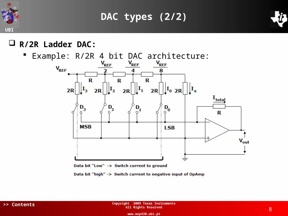
DAC types (1/2)
Binary Weighted DAC: Contains one resistor (or current source) for each bit of the
DAC connected to a common voltage source VREF; There are accuracy problems (high precision resistors are
required);
R/2R Ladder DAC: Binary weighted DAC that uses a repeating cascaded
structure of resistors of value R and 2R; The MSP430’s DAC12 module uses this architecture.
UBI
>> Contents8
Copyright 2009 Texas Instruments All Rights Reserved
www.msp430.ubi.pt
DAC types (2/2)
R/2R Ladder DAC: Example: R/2R 4 bit DAC architecture:

UBI
>> Contents9
Copyright 2009 Texas Instruments All Rights Reserved
www.msp430.ubi.pt
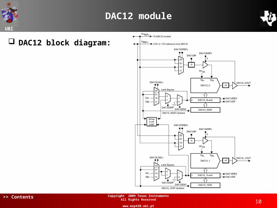
DAC12 module
The 12 bit DAC12 module is a voltage output DAC;
All the MSP430 hardware development tools contain this module;
The MSP430FG4618 device on the Experimenter’s board has two DAC12 modules, allowing them to be grouped together for synchronous update operation.
UBI
>> Contents10
Copyright 2009 Texas Instruments All Rights Reserved
www.msp430.ubi.pt
DAC12 module
DAC12 block diagram:
UBI
>> Contents11
Copyright 2009 Texas Instruments All Rights Reserved
www.msp430.ubi.pt
DAC12 features
12 bit monotonic output;
8-bit or 12-bit voltage output resolution;
Programmable settling time vs. power consumption;
Internal or external reference selection;
Straight binary or Two’s complement data format;
Self-calibration option for offset correction;
Synchronized update capability for multiple DAC12s;
Direct Memory Access (DMA) enable.

UBI
>> Contents12
Copyright 2009 Texas Instruments All Rights Reserved
www.msp430.ubi.pt
DAC12 operation (1/4)
DAC12 core: Dynamic range controlled by:
• DAC’s resolution: 8 bits or 12 bits (DAC12RES bit);• Full-scale output: 1xVREF or 3xVREF (DAC12IR bit);
• Input data format: straight binary or two’s complement (DAC12DF bit).
The output voltage (straight binary data format):Resolution DAC12RES DAC12IR Output voltage
12 bit 0 0
4096_12
3xDATDAC
VV REFOUT
12 bit 0 1
4096_12 xDATDAC
VV REFOUT
8 bit 1 0
256_12
3xDATDAC
VV REFOUT
8 bit 1 1
256_12 xDATDAC
VV REFOUT
UBI
>> Contents13
Copyright 2009 Texas Instruments All Rights Reserved
www.msp430.ubi.pt
DAC12 operation (2/4)
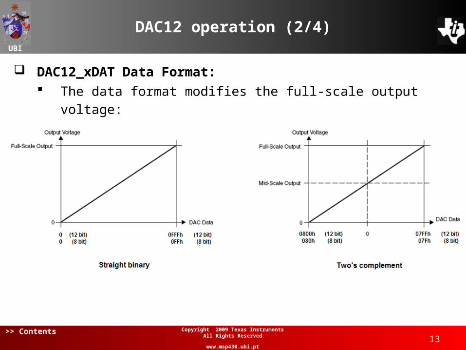
DAC12_xDAT Data Format:
The data format modifies the full-scale output voltage:
UBI
>> Contents14
Copyright 2009 Texas Instruments All Rights Reserved
www.msp430.ubi.pt
DAC12 operation (3/4)
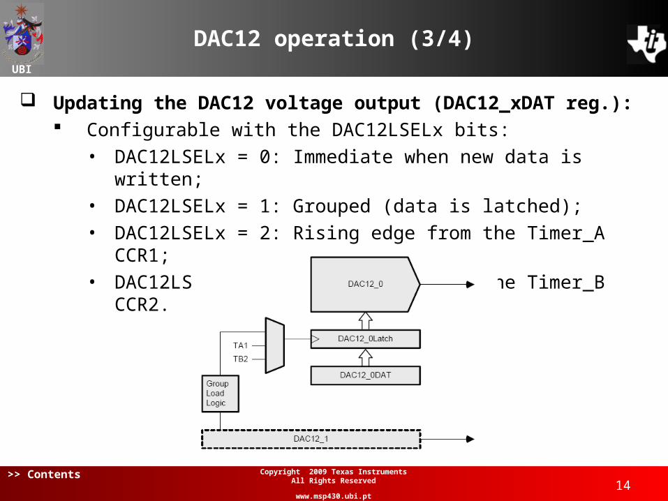
Updating the DAC12 voltage output (DAC12_xDAT reg.): Configurable with the DAC12LSELx bits:
• DAC12LSELx = 0: Immediate when new data is written;• DAC12LSELx = 1: Grouped (data is latched);• DAC12LSELx = 2: Rising edge from the Timer_A CCR1;• DAC12LSELx = 3: Rising edge from the Timer_B CCR2.
UBI
>> Contents15
Copyright 2009 Texas Instruments All Rights Reserved
www.msp430.ubi.pt
DAC12 operation (4/4)
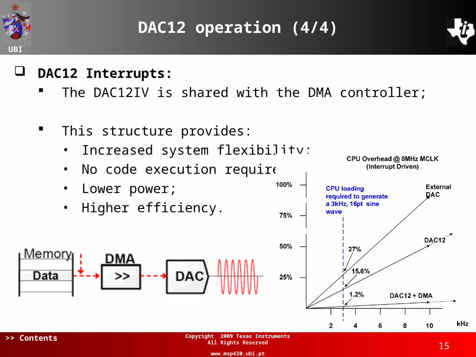
DAC12 Interrupts: The DAC12IV is shared with the DMA controller;
This structure provides:• Increased system flexibility;• No code execution required;• Lower power;• Higher efficiency.
UBI
>> Contents16
Copyright 2009 Texas Instruments All Rights Reserved
www.msp430.ubi.pt
DAC12 Registers (1/3)
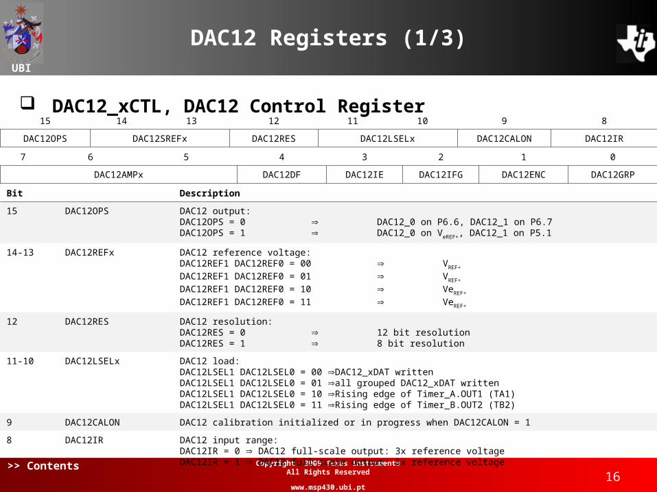
DAC12_xCTL, DAC12 Control Register 15 14 13 12 11 10 9 8
DAC12OPS DAC12SREFx DAC12RES DAC12LSELx DAC12CALON DAC12IR
7 6 5 4 3 2 1 0
DAC12AMPx DAC12DF DAC12IE DAC12IFG DAC12ENC DAC12GRP
Bit Description
15 DAC12OPS DAC12 output:DAC12OPS = 0 DAC12_0 on P6.6, DAC12_1 on P6.7DAC12OPS = 1 DAC12_0 on VeREF+, DAC12_1 on P5.1
14-13 DAC12REFx DAC12 reference voltage:DAC12REF1 DAC12REF0 = 00 VREF+
DAC12REF1 DAC12REF0 = 01 VREF+
DAC12REF1 DAC12REF0 = 10 VeREF+
DAC12REF1 DAC12REF0 = 11 VeREF+
12 DAC12RES DAC12 resolution:DAC12RES = 0 12 bit resolutionDAC12RES = 1 8 bit resolution
11-10 DAC12LSELx DAC12 load:DAC12LSEL1 DAC12LSEL0 = 00 DAC12_xDAT writtenDAC12LSEL1 DAC12LSEL0 = 01 all grouped DAC12_xDAT writtenDAC12LSEL1 DAC12LSEL0 = 10 Rising edge of Timer_A.OUT1 (TA1)DAC12LSEL1 DAC12LSEL0 = 11 Rising edge of Timer_B.OUT2 (TB2)
9 DAC12CALON DAC12 calibration initialized or in progress when DAC12CALON = 1
8 DAC12IR DAC12 input range:DAC12IR = 0 DAC12 full-scale output: 3x reference voltageDAC12IR = 1 DAC12 full-scale output: 1x reference voltage
UBI
>> Contents17
Copyright 2009 Texas Instruments All Rights Reserved
www.msp430.ubi.pt
DAC12 Registers (2/3)
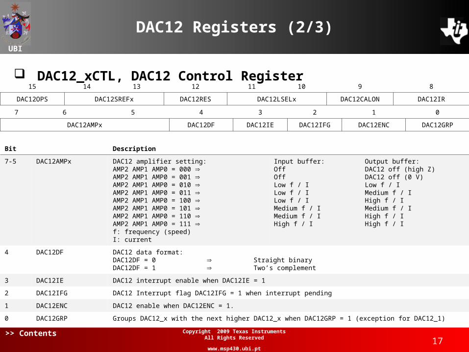
DAC12_xCTL, DAC12 Control Register 15 14 13 12 11 10 9 8
DAC12OPS DAC12SREFx DAC12RES DAC12LSELx DAC12CALON DAC12IR
7 6 5 4 3 2 1 0
DAC12AMPx DAC12DF DAC12IE DAC12IFG DAC12ENC DAC12GRP
Bit Description
7-5 DAC12AMPx DAC12 amplifier setting:AMP2 AMP1 AMP0 = 000 AMP2 AMP1 AMP0 = 001 AMP2 AMP1 AMP0 = 010 AMP2 AMP1 AMP0 = 011 AMP2 AMP1 AMP0 = 100 AMP2 AMP1 AMP0 = 101 AMP2 AMP1 AMP0 = 110 AMP2 AMP1 AMP0 = 111 f: frequency (speed)I: current
Input buffer:OffOffLow f / ILow f / ILow f / IMedium f / IMedium f / IHigh f / I
Output buffer:DAC12 off (high Z)DAC12 off (0 V)Low f / IMedium f / IHigh f / IMedium f / IHigh f / IHigh f / I
4 DAC12DF DAC12 data format:DAC12DF = 0 Straight binaryDAC12DF = 1 Two’s complement
3 DAC12IE DAC12 interrupt enable when DAC12IE = 1
2 DAC12IFG DAC12 Interrupt flag DAC12IFG = 1 when interrupt pending
1 DAC12ENC DAC12 enable when DAC12ENC = 1.
0 DAC12GRP Groups DAC12_x with the next higher DAC12_x when DAC12GRP = 1 (exception for DAC12_1)

UBI
>> Contents18
Copyright 2009 Texas Instruments All Rights Reserved
www.msp430.ubi.pt
DAC12 Registers (3/3)
DAC12_xDAT, DAC12 Data Register The four most significant bits (bits 15 – 12) are always zero;
The twelve least significant bits store the DAC12 data (bits 11 – 0);
The DAC12 data is right justified, but the MSB depends on:• Resolution:
– 8 bit: Bit 7;– 12 bit: Bit 11.
• Data format:– Straight binary: MSB is data;– Two’s complement: MSB is sign.
UBI
>> Contents19
Copyright 2009 Texas Instruments All Rights Reserved
www.msp430.ubi.pt
DMA capability (1/2)
The MSP430 has been designed for applications requiring low power;
When the application requires data-handling, the direct memory access (DMA) capability included in some devices is useful: 5xxx; FG4xx(x); F261x; F16x(x) and F15x; Among these: MSP430FG4618 (Experimenter’s board).
DMA automatically handles data;
DMA does not require CPU intervention;
DMA helps reduce the power consumption (CPU remains sleeping).
UBI
>> Contents20
Copyright 2009 Texas Instruments All Rights Reserved
www.msp430.ubi.pt
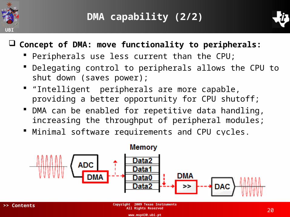
DMA capability (2/2)
Concept of DMA: move functionality to peripherals: Peripherals use less current than the CPU; Delegating control to peripherals allows the CPU to shut
down (saves power); “Intelligent” peripherals are more capable, providing a
better opportunity for CPU shutoff; DMA can be enabled for repetitive data handling, increasing
the throughput of peripheral modules; Minimal software requirements and CPU cycles.
UBI
>> Contents21
Copyright 2009 Texas Instruments All Rights Reserved
www.msp430.ubi.pt
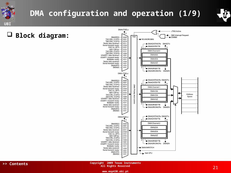
DMA configuration and operation (1/9)
Block diagram:
UBI
>> Contents22
Copyright 2009 Texas Instruments All Rights Reserved
www.msp430.ubi.pt
DMA configuration and operation (2/9)
DMA controller features: Three independent transfer channels;
Configurable (ROUNDROBIN bit) DMA channel priorities:• Default: DMA0−DMA1−DMA2;
DMA Transfer cycle time:• Requires only two MCLK clock cycles per transfer;• Each byte/word transfer requires:
– 2 MCLK cycles after synchronization;– 1 MCKL cycle of wait time after transfer.
UBI
>> Contents23
Copyright 2009 Texas Instruments All Rights Reserved
www.msp430.ubi.pt
DMA configuration and operation (3/9)
DMA controller features: Block sizes up to 65535 bytes or words;
Configurable edge/level-triggered transfer (DMALEVEL bit).
Byte or word and mixed byte/word transfer capability:• Byte-to-byte;• Word-to-word;• Byte-to-word (upper byte of the destination word is
cleared);• Word-to-byte (lower byte of the source word is
transferred).
UBI
>> Contents24
Copyright 2009 Texas Instruments All Rights Reserved
www.msp430.ubi.pt
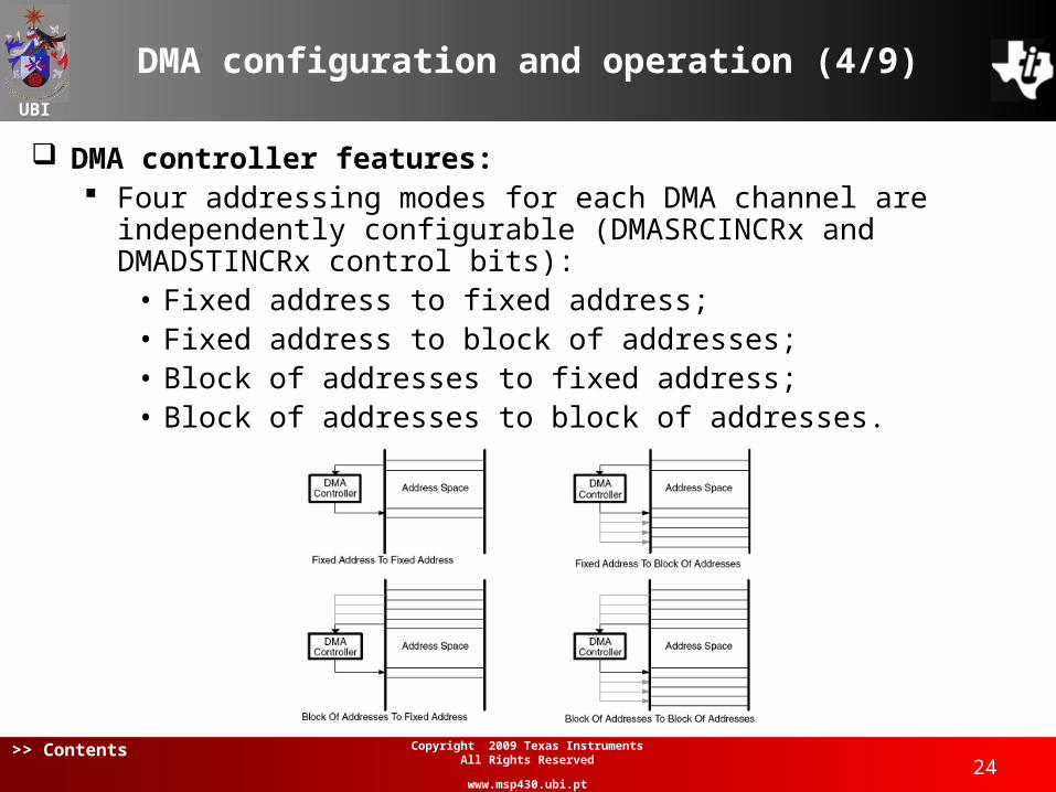
DMA configuration and operation (4/9)
DMA controller features: Four addressing modes for each DMA channel are
independently configurable (DMASRCINCRx and DMADSTINCRx control bits):
• Fixed address to fixed address;• Fixed address to block of addresses;• Block of addresses to fixed address;• Block of addresses to block of addresses.
UBI
>> Contents25
Copyright 2009 Texas Instruments All Rights Reserved
www.msp430.ubi.pt
DMA configuration and operation (5/9)
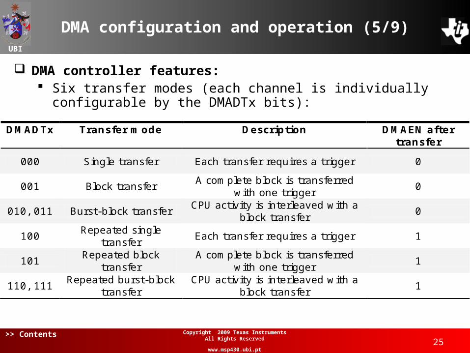
DMA controller features: Six transfer modes (each channel is individually configurable
by the DMADTx bits):
DMADTx Transfer mode Description DMAEN after transfer
000 Single transfer Each transfer requires a trigger 0
001 Block transfer A complete block is transferred
with one trigger 0
010, 011 Burst-block transfer CPU activity is interleaved with a
block transfer 0
100 Repeated single
transfer Each transfer requires a trigger 1
101 Repeated block
transfer A complete block is transferred
with one trigger 1
110, 111 Repeated burst-block
transfer CPU activity is interleaved with a
block transfer 1
UBI
>> Contents26
Copyright 2009 Texas Instruments All Rights Reserved
www.msp430.ubi.pt
DMA configuration and operation (6/9)
System interrupts: DMA transfers are not interruptible by system interrupts, but
system ISRs can be interrupted by DMA transfers;
Only NMI interrupts can be given priority over the DMA controller (ENNMI bit is set). If the ENNMI bit is not set, system interrupts remain pending until the completion of the transfer.
DMA controller interrupts: Each DMA channel has its own DMAIFG flag that is set when
the corresponding DMAxSZ register counts to zero (all modes);
If the corresponding DMAIE and GIE bits are set, an interrupt request is generated.
UBI
>> Contents27
Copyright 2009 Texas Instruments All Rights Reserved
www.msp430.ubi.pt
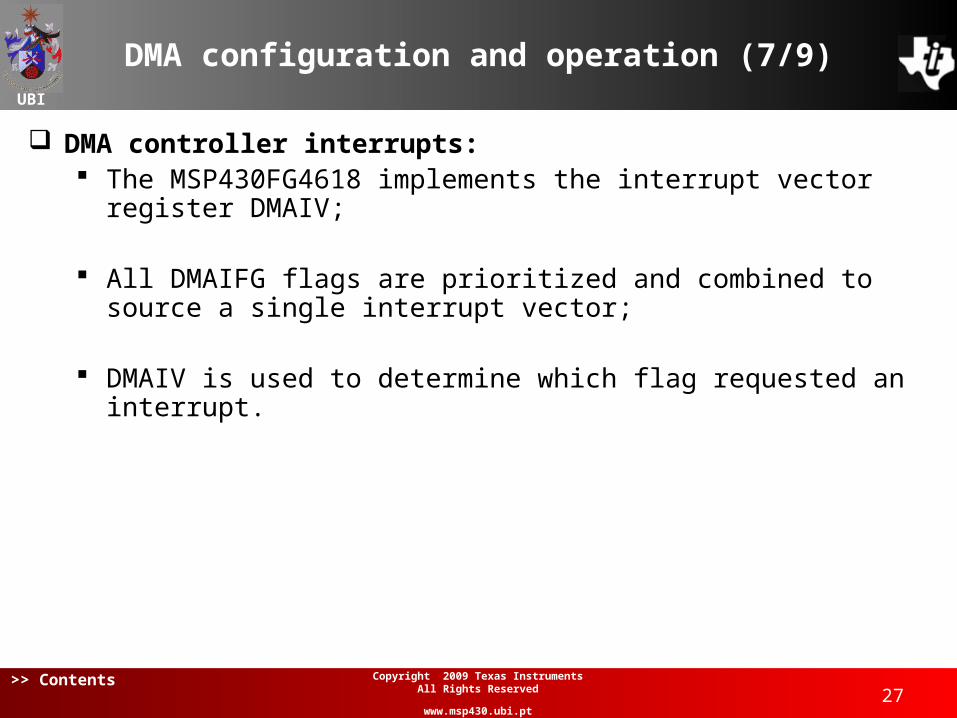
DMA configuration and operation (7/9)
DMA controller interrupts: The MSP430FG4618 implements the interrupt vector register
DMAIV;
All DMAIFG flags are prioritized and combined to source a single interrupt vector;
DMAIV is used to determine which flag requested an interrupt.
UBI
>> Contents28
Copyright 2009 Texas Instruments All Rights Reserved
www.msp430.ubi.pt
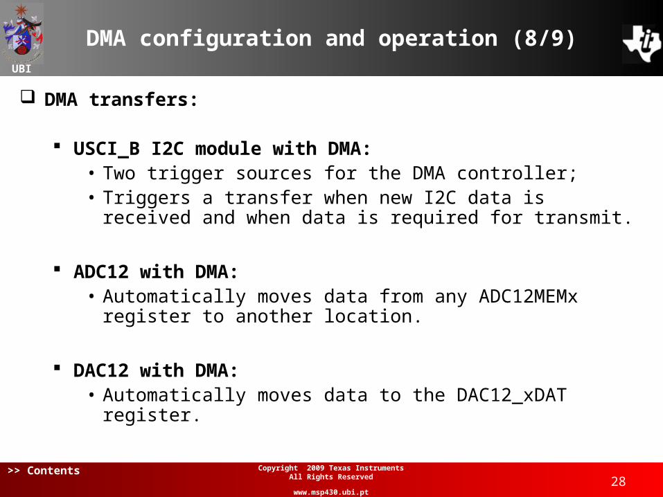
DMA configuration and operation (8/9)
DMA transfers:
USCI_B I2C module with DMA:• Two trigger sources for the DMA controller;• Triggers a transfer when new I2C data is received and
when data is required for transmit.
ADC12 with DMA:• Automatically moves data from any ADC12MEMx register
to another location.
DAC12 with DMA:• Automatically moves data to the DAC12_xDAT register.
UBI
>> Contents29
Copyright 2009 Texas Instruments All Rights Reserved
www.msp430.ubi.pt
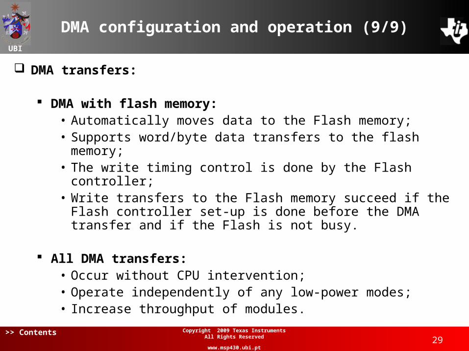
DMA configuration and operation (9/9)
DMA transfers:
DMA with flash memory:• Automatically moves data to the Flash memory;• Supports word/byte data transfers to the flash memory;• The write timing control is done by the Flash controller;• Write transfers to the Flash memory succeed if the Flash
controller set-up is done before the DMA transfer and if the Flash is not busy.
All DMA transfers:• Occur without CPU intervention;• Operate independently of any low-power modes;• Increase throughput of modules.
UBI
>> Contents30
Copyright 2009 Texas Instruments All Rights Reserved
www.msp430.ubi.pt
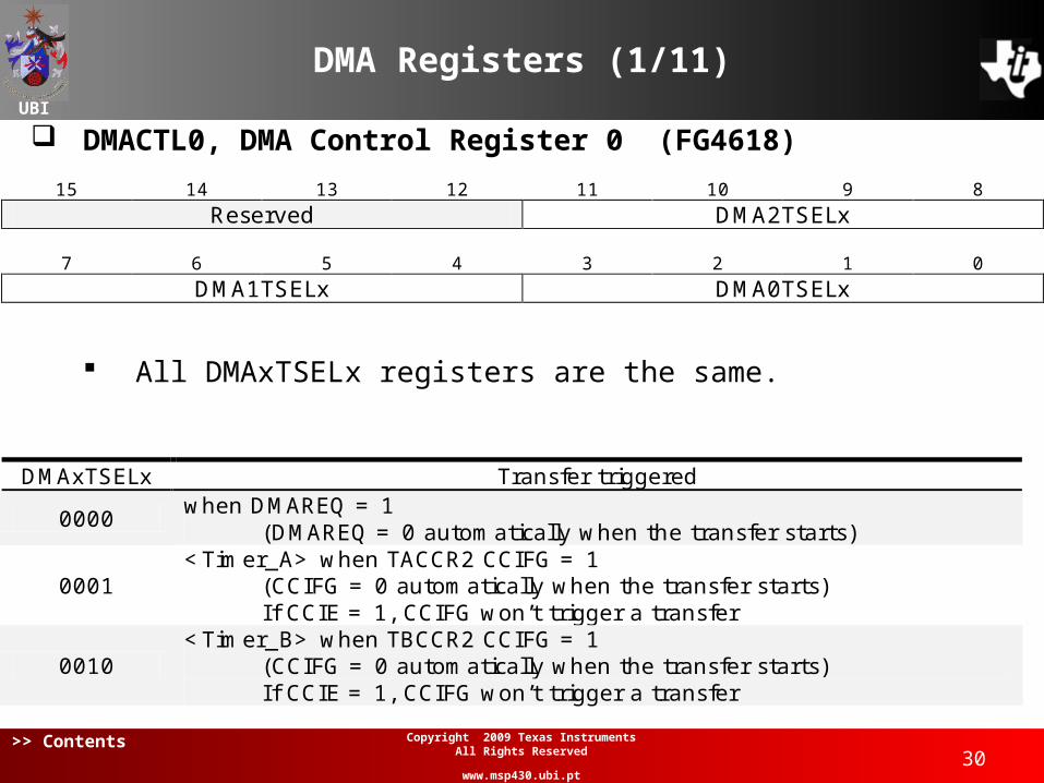
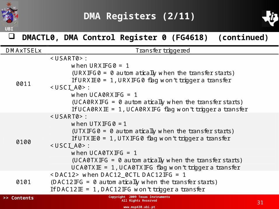
DMA Registers (1/11)
DMACTL0, DMA Control Register 0 (FG4618)
All DMAxTSELx registers are the same.
15 14 13 12 11 10 9 8
Reserved DMA2TSELx
7 6 5 4 3 2 1 0
DMA1TSELx DMA0TSELx
DMAxTSELx Transfer triggered
0000 when DMAREQ = 1 (DMAREQ = 0 automatically when the transfer starts)
0001 <Timer_A> when TACCR2 CCIFG = 1 (CCIFG = 0 automatically when the transfer starts) I f CCIE = 1, CCIFG won’t trigger a transfer
0010 <Timer_B> when TBCCR2 CCIFG = 1 (CCIFG = 0 automatically when the transfer starts) I f CCIE = 1, CCIFG won’t trigger a transfer
UBI
>> Contents31
Copyright 2009 Texas Instruments All Rights Reserved
www.msp430.ubi.pt
DMA Registers (2/11)
DMACTL0, DMA Control Register 0 (FG4618) (continued)
DMAxTSELx Transfer triggered
0011
<USART0>: when URXIFG0 = 1 (URXIFG0 = 0 automatically when the transfer starts) I f URXIE0 = 1, URXIFG0 flag won’t trigger a transfer <USCI_A0>: when UCA0RXIFG = 1 (UCA0RXIFG = 0 automatically when the transfer starts) I f UCA0RXIE = 1, UCA0RXIFG flag won’t trigger a transfer
0100
<USART0>: when UTXIFG0 =1 (UTXIFG0 = 0 automatically when the transfer starts) I f UTXIE0 = 1, UTXIFG0 flag won’t trigger a transfer <USCI_A0>: when UCA0TXIFG = 1 (UCA0TXIFG = 0 automatically when the transfer starts) UCA0TXIE = 1, UCA0TXIFG flag won’t trigger a transfer
0101 <DAC12> when DAC12_0CTL DAC12IFG = 1 (DAC12IFG = 0 automatically when the transfer starts) I f DAC12IE = 1, DAC12IFG won’t trigger a transfer
UBI
>> Contents32
Copyright 2009 Texas Instruments All Rights Reserved
www.msp430.ubi.pt
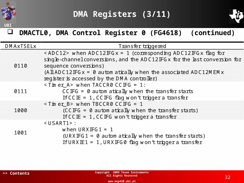
DMA Registers (3/11)
DMACTL0, DMA Control Register 0 (FG4618) (continued)
DMAxTSELx Transfer triggered
0110
<ADC12> when ADC12IFGx = 1 (corresponding ADC12IFGx flag for single-channel conversions, and the ADC12IFGx for the last conversion for sequence conversions) (All ADC12IFGx = 0 automatically when the associated ADC12MEMx register is accessed by the DMA controller)
0111 <Timer_A> when TACCR0 CCIFG = 1: CCIFG = 0 automatically when the transfer starts I f CCIE = 1, CCIFG flag won’t trigger a transfer
1000 <Timer_B> when TBCCR0 CCIFG = 1 (CCIFG = 0 automatically when the transfer starts) I f CCIE = 1, CCIFG won’t trigger a transfer
1001
<USART1>: when URXIFG1 = 1 (URXIFG1 = 0 automatically when the transfer starts) I f URXIE1 = 1, URXIFG0 flag won’t trigger a transfer
UBI
>> Contents33
Copyright 2009 Texas Instruments All Rights Reserved
www.msp430.ubi.pt
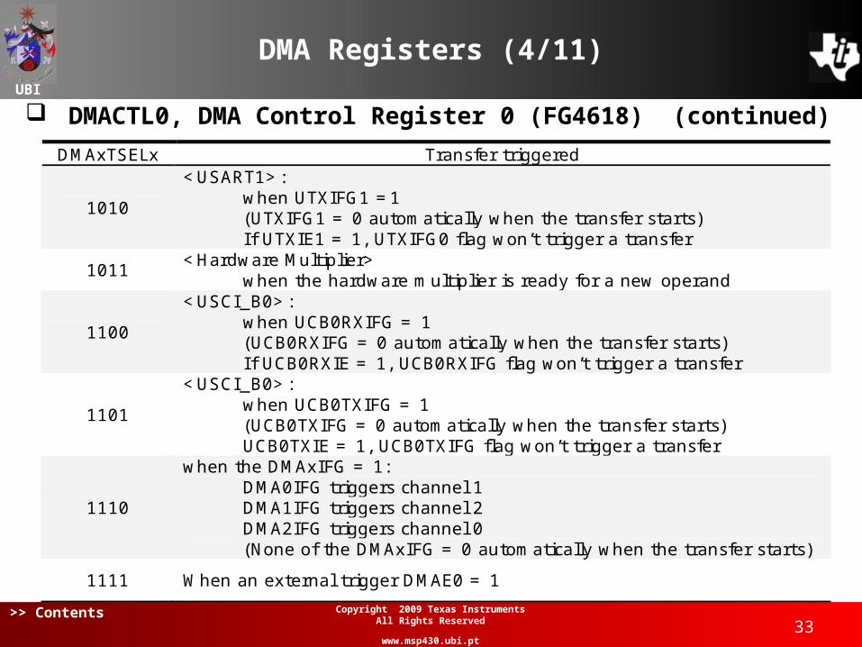
DMA Registers (4/11)
DMACTL0, DMA Control Register 0 (FG4618) (continued)
DMAxTSELx Transfer triggered
1010
<USART1>: when UTXIFG1 =1 (UTXIFG1 = 0 automatically when the transfer starts) I f UTXIE1 = 1, UTXIFG0 flag won’t trigger a transfer
1011 <Hardware Multiplier> when the hardware multiplier is ready for a new operand
1100
<USCI_B0>: when UCB0RXIFG = 1 (UCB0RXIFG = 0 automatically when the transfer starts) I f UCB0RXIE = 1, UCB0RXIFG flag won’t trigger a transfer
1101
<USCI_B0>: when UCB0TXIFG = 1 (UCB0TXIFG = 0 automatically when the transfer starts) UCB0TXIE = 1, UCB0TXIFG flag won’t trigger a transfer
1110
when the DMAxIFG = 1: DMA0IFG triggers channel 1 DMA1IFG triggers channel 2 DMA2IFG triggers channel 0 (None of the DMAxIFG = 0 automatically when the transfer starts)
1111 When an external trigger DMAE0 = 1
UBI
>> Contents34
Copyright 2009 Texas Instruments All Rights Reserved
www.msp430.ubi.pt
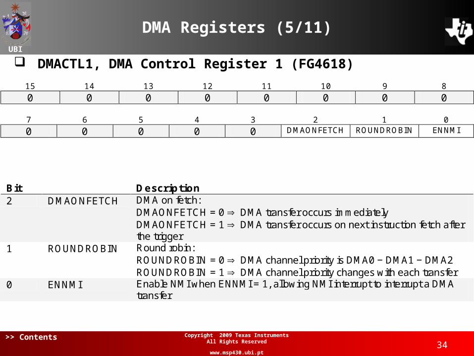
DMA Registers (5/11)
DMACTL1, DMA Control Register 1 (FG4618)
15 14 13 12 11 10 9 8
0 0 0 0 0 0 0 0
7 6 5 4 3 2 1 0
0 0 0 0 0 DMAONFETCH ROUNDROBIN ENNMI
Bit Description 2 DMAONFETCH DMA on fetch:
DMAONFETCH = 0 DMA transfer occurs immediately DMAONFETCH = 1 DMA transfer occurs on next instruction fetch after the trigger
1 ROUNDROBIN Round robin: ROUNDROBIN = 0 DMA channel priority is DMA0 − DMA1 − DMA2 ROUNDROBIN = 1 DMA channel priority changes with each transfer
0 ENNMI Enable NMI when ENNMI = 1, allowing NMI interrupt to interrupt a DMA transfer
UBI
>> Contents35
Copyright 2009 Texas Instruments All Rights Reserved
www.msp430.ubi.pt
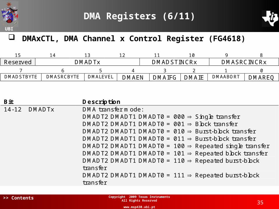
DMA Registers (6/11)
DMAxCTL, DMA Channel x Control Register (FG4618)
15 14 13 12 11 10 9 8
Reserved DMADTx DMADSTINCRx DMASRCINCRx
7 6 5 4 3 2 1 0 DMADSTBYTE DMASRCBYTE DMALEVEL DMAEN DMAIFG DMAIE DMAABORT DMAREQ
Bit Description 14-12 DMADTx DMA transfer mode:
DMADT2 DMADT1 DMADT0 = 000 Single transfer DMADT2 DMADT1 DMADT0 = 001 Block transfer DMADT2 DMADT1 DMADT0 = 010 Burst-block transfer DMADT2 DMADT1 DMADT0 = 011 Burst-block transfer DMADT2 DMADT1 DMADT0 = 100 Repeated single transfer DMADT2 DMADT1 DMADT0 = 101 Repeated block transfer DMADT2 DMADT1 DMADT0 = 110 Repeated burst-block transfer DMADT2 DMADT1 DMADT0 = 111 Repeated burst-block transfer
UBI
>> Contents36
Copyright 2009 Texas Instruments All Rights Reserved
www.msp430.ubi.pt
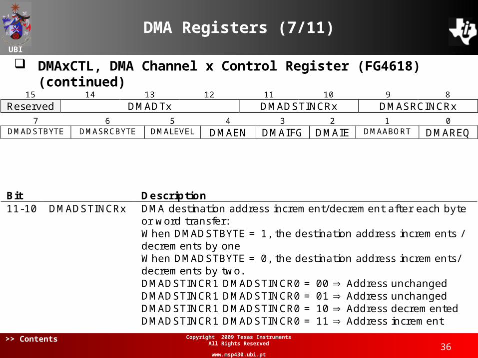
DMA Registers (7/11)
DMAxCTL, DMA Channel x Control Register (FG4618) (continued)
15 14 13 12 11 10 9 8
Reserved DMADTx DMADSTINCRx DMASRCINCRx
7 6 5 4 3 2 1 0 DMADSTBYTE DMASRCBYTE DMALEVEL DMAEN DMAIFG DMAIE DMAABORT DMAREQ
Bit Description 11-10 DMADSTINCRx DMA destination address increment/decrement after each byte
or word transfer: When DMADSTBYTE = 1, the destination address increments / decrements by one When DMADSTBYTE = 0, the destination address increments/ decrements by two. DMADSTINCR1 DMADSTINCR0 = 00 Address unchanged DMADSTINCR1 DMADSTINCR0 = 01 Address unchanged DMADSTINCR1 DMADSTINCR0 = 10 Address decremented DMADSTINCR1 DMADSTINCR0 = 11 Address increment
UBI
>> Contents37
Copyright 2009 Texas Instruments All Rights Reserved
www.msp430.ubi.pt
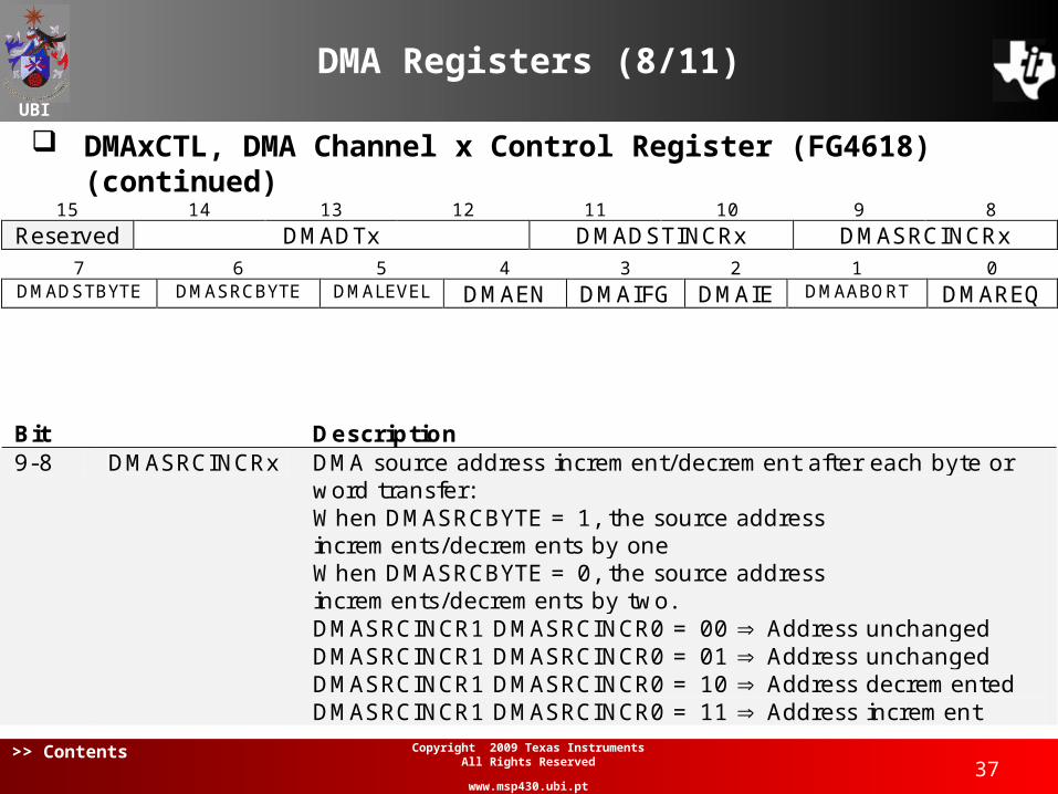
DMA Registers (8/11)
DMAxCTL, DMA Channel x Control Register (FG4618) (continued)
15 14 13 12 11 10 9 8
Reserved DMADTx DMADSTINCRx DMASRCINCRx
7 6 5 4 3 2 1 0 DMADSTBYTE DMASRCBYTE DMALEVEL DMAEN DMAIFG DMAIE DMAABORT DMAREQ
Bit Description 9-8 DMASRCINCRx DMA source address increment/decrement after each byte or
word transfer: When DMASRCBYTE = 1, the source address increments/decrements by one When DMASRCBYTE = 0, the source address increments/decrements by two. DMASRCINCR1 DMASRCINCR0 = 00 Address unchanged DMASRCINCR1 DMASRCINCR0 = 01 Address unchanged DMASRCINCR1 DMASRCINCR0 = 10 Address decremented DMASRCINCR1 DMASRCINCR0 = 11 Address increment
UBI
>> Contents38
Copyright 2009 Texas Instruments All Rights Reserved
www.msp430.ubi.pt
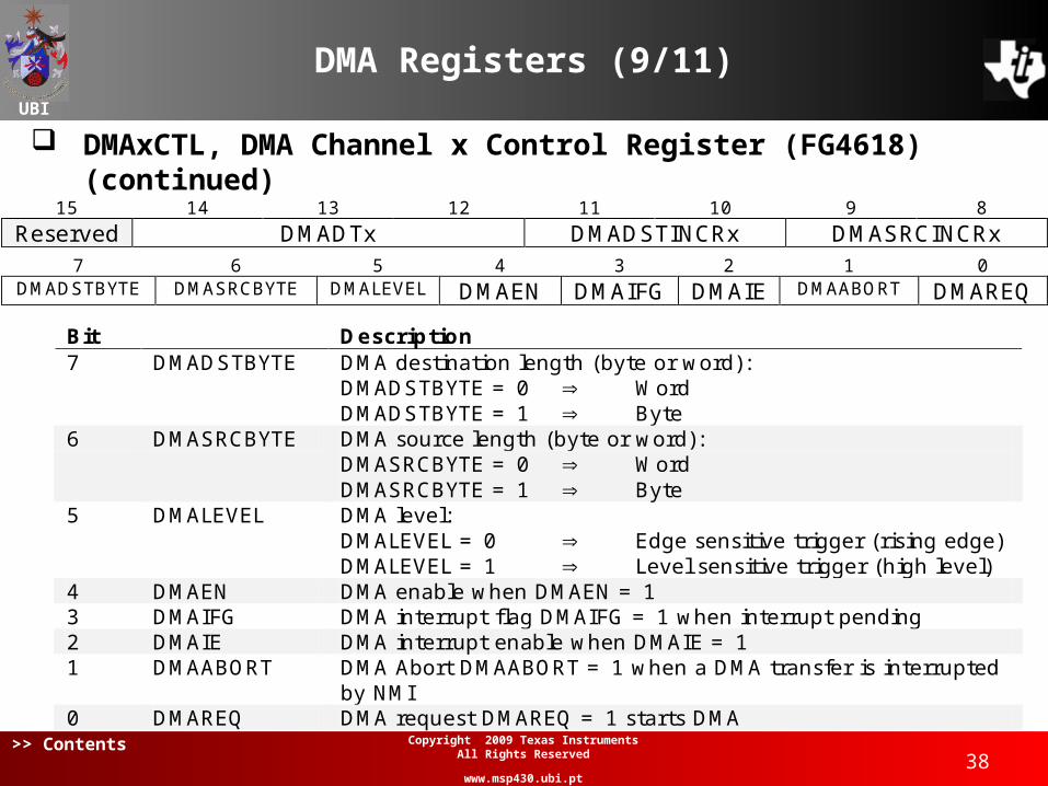
DMA Registers (9/11)
DMAxCTL, DMA Channel x Control Register (FG4618) (continued)
15 14 13 12 11 10 9 8
Reserved DMADTx DMADSTINCRx DMASRCINCRx
7 6 5 4 3 2 1 0 DMADSTBYTE DMASRCBYTE DMALEVEL DMAEN DMAIFG DMAIE DMAABORT DMAREQ
Bit Description 7 DMADSTBYTE DMA destination length (byte or word):
DMADSTBYTE = 0 Word DMADSTBYTE = 1 Byte
6 DMASRCBYTE DMA source length (byte or word): DMASRCBYTE = 0 Word DMASRCBYTE = 1 Byte
5 DMALEVEL DMA level: DMALEVEL = 0 Edge sensitive trigger (rising edge) DMALEVEL = 1 Level sensitive trigger (high level)
4 DMAEN DMA enable when DMAEN = 1 3 DMAIFG DMA interrupt flag DMAIFG = 1 when interrupt pending 2 DMAIE DMA interrupt enable when DMAIE = 1 1 DMAABORT DMA Abort DMAABORT = 1 when a DMA transfer is interrupted
by NMI 0 DMAREQ DMA request DMAREQ = 1 starts DMA
UBI
>> Contents39
Copyright 2009 Texas Instruments All Rights Reserved
www.msp430.ubi.pt
DMA Registers (10/11)
DMAxSA, DMA Source Address Register (FG4618) 32-bit register points to the DMA source address for single
transfers or the first source address for block transfers.
DMAxDA, DMA Destination Address Register (FG4618) 32-bit register points to the DMA destination address for
single transfers or the first source address for block transfers.
For both registers (DMAxSA and DMAxDA):• Bits 31−20 are reserved and always read as zero;• Reading or writing to bits 19-16 requires the use of
extended instructions;• When writing to DMAxSA or DMAxDA with word
instructions, bits 19-16 are cleared.
UBI
>> Contents40
Copyright 2009 Texas Instruments All Rights Reserved
www.msp430.ubi.pt
DMA Registers (11/11)
DMAxSZ, DMA Size Address Register (FG4618) The 16-bit DMA size address register defines the number of
bytes/words of data per block transfer:• DMAxSZ decrements with each word or byte transfer;• When DMAxSZ = 0, it is immediately and automatically
reloaded with its previously initialized value.
DMAIV, DMA Interrupt Vector Register (FG4618) 16 bit DMAIV value only uses bits 3 to 1 (other bits = 0); DMAIV content provides the interrupt source priority:
DMAIV = 02h: DMA channel 0 (highest priority);DMAIV = 04h: DMA channel 1;DMAIV = 06h: DMA channel 2;…DMAIV = 0Eh: Reserved (lowest priority).
UBI
>> Contents41
Copyright 2009 Texas Instruments All Rights Reserved
www.msp430.ubi.pt
Hardware Multiplier Introduction (1/3)
Several devices in the MSP430 family contain a hardware multiplier peripheral module:
• 54xx;• FG46xx;• FE42x(A);• F47xx; F44X; F42x(A);• F261x; F24x(x);• F16x(x).
The MSP430FG4618 (Experimenter’s board) supports multiplications using the Hardware Multiplier module, without interfering with CPU activities.
UBI
>> Contents42
Copyright 2009 Texas Instruments All Rights Reserved
www.msp430.ubi.pt
Hardware Multiplier Introduction (2/3)
The hardware multiplier supports: Unsigned multiply (MPY); Signed multiply (MPYS); Unsigned multiply accumulate (MAC); Signed multiply accumulate (MACS).
The multiplication operation can be: 16×16 bits; 16×8 bits; 8×16 bits; 8×8 bits.
• Operands are written to two registers, each one with 8 bits or 16 bits.
UBI
>> Contents43
Copyright 2009 Texas Instruments All Rights Reserved
www.msp430.ubi.pt
Hardware Multiplier Introduction (3/3)
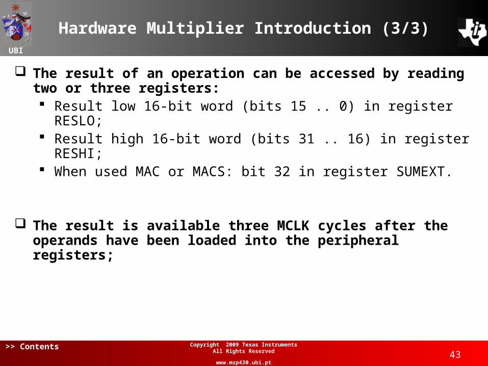
The result of an operation can be accessed by reading two or three registers: Result low 16-bit word (bits 15 .. 0) in register RESLO; Result high 16-bit word (bits 31 .. 16) in register RESHI; When used MAC or MACS: bit 32 in register SUMEXT.
The result is available three MCLK cycles after the operands have been loaded into the peripheral registers;
UBI
>> Contents44
Copyright 2009 Texas Instruments All Rights Reserved
www.msp430.ubi.pt
Hardware Multiplier Structure (1/4)
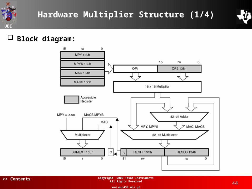
Block diagram:
UBI
>> Contents45
Copyright 2009 Texas Instruments All Rights Reserved
www.msp430.ubi.pt
Hardware Multiplier Structure (2/4)
Two 16-bit operand registers: First operand register, OP1:
• Has four addresses used to select the multiply mode:
Second operand register, OP2:• Writing to the register initiates the multiply operation.
Register name Multiplication operation OP1 Address
MPY Unsigned multiply 0130h
MPYS Signed multiply 0132h
MAC Unsigned multiply accumulate 0134h
MACS Signed multiply accumulate 0136h
UBI
>> Contents46
Copyright 2009 Texas Instruments All Rights Reserved
www.msp430.ubi.pt
Hardware Multiplier Structure (3/4)
Three result registers, RESLO, RESHI, and SUMEXT: RESLO stores the low word of the result; RESHI stores the high word of the result:
• The contents of RESHI depend on the multiply operation:
Multiplication operation RESHI content
Unsigned multiply (MPY) Upper 16-bits of the result
Signed multiply (MPYS) Bit 15 (MSB): sign Bits 14 - 0: upper 15-bits of the result Data format: Two’s complement
Unsigned multiply accumulate (MAC) Upper 16-bits of the result
Signed multiply accumulate (MACS) Upper 16-bits of the result Data format: Two’s complement
UBI
>> Contents47
Copyright 2009 Texas Instruments All Rights Reserved
www.msp430.ubi.pt
Hardware Multiplier Structure (4/4)
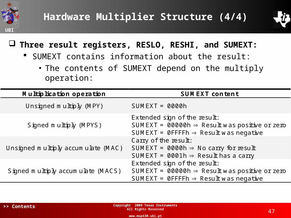
Three result registers, RESLO, RESHI, and SUMEXT: SUMEXT contains information about the result:
• The contents of SUMEXT depend on the multiply operation:
Multiplication operation SUMEXT content
Unsigned multiply (MPY) SUMEXT = 0000h
Signed multiply (MPYS) Extended sign of the result: SUMEXT = 00000h Result was positive or zero SUMEXT = 0FFFFh Result was negative
Unsigned multiply accumulate (MAC) Carry of the result: SUMEXT = 0000h No carry for result SUMEXT = 0001h Result has a carry
Signed multiply accumulate (MACS) Extended sign of the result: SUMEXT = 00000h Result was positive or zero SUMEXT = 0FFFFh Result was negative
UBI
>> Contents
Multiplication Operation (1/2)
Unsigned Multiply (MPY) The two operands are treated as unsigned numbers
• In the range 00000h (smallest number) to 0FFFFh (largest number)
The maximum possible result is obtained with input operands 0FFFFh and 0FFFFh:
• 0FFFFh x 0FFFFh = 0FFFE0001h No carry is possible and the SUMEXT register always
contains zero
Signed Multiply (MPYS) The two operands are treated as signed Two’s
complement numbers• In the range 08000h (most negative number, –32768
in decimal) to 07FFFh (most positive number, +32767 in decimal)
48 Copyright 2009 Texas Instruments
All Rights Reserved
www.msp430.ubi.pt
UBI
>> Contents
Multiplication Operation (2/2)
The SUMEXT register contains the extended sign of the calculated result:
• SUMEXT = 00000h: the result is positive• SUMEXT = 0FFFFh: the result is negative
Multiply-and-Accumulate (MAC) The two operands are treated as unsigned numbers (0h
to 0FFFFh) The maximum possible result is obtained with input
operands 0FFFFh and 0FFFFh:• 0FFFFh x 0FFFFh = 0FFFE0001h
This result is added to the previous contents of the two sum registers (SUMLO and SUMHI)
• SUMEXT = 00000h: no carry occurred• SUMEXT = 00001h: a carry occurred
49 Copyright 2009 Texas Instruments
All Rights Reserved
www.msp430.ubi.pt
UBI
>> Contents50
Copyright 2009 Texas Instruments All Rights Reserved
www.msp430.ubi.pt
Hardware Multiplier Registers
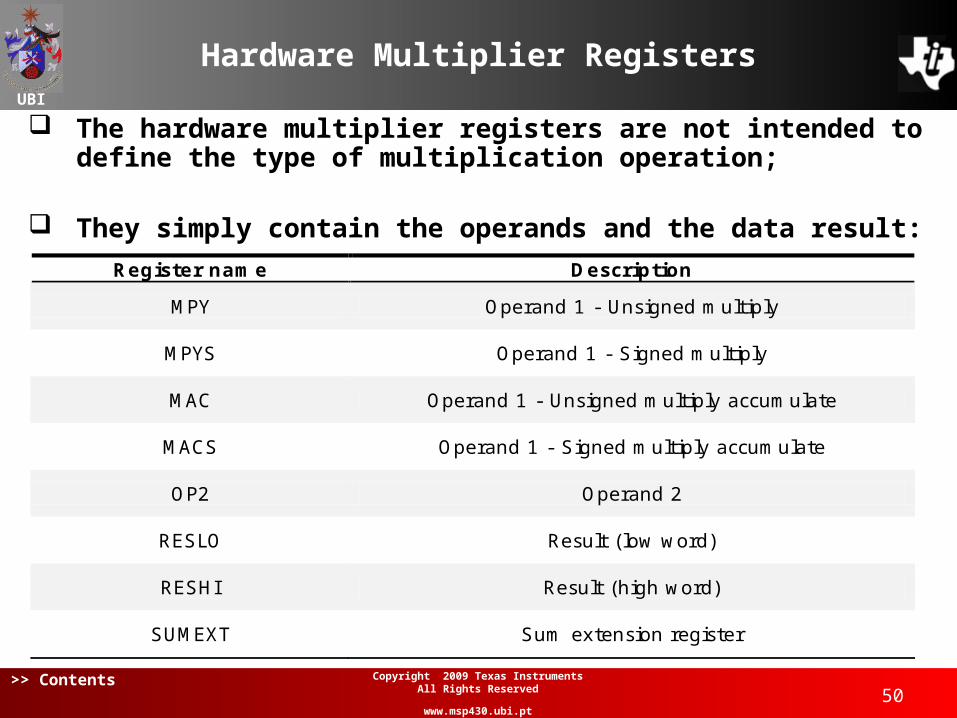
The hardware multiplier registers are not intended to define the type of multiplication operation;
They simply contain the operands and the data result:
Register name Description
MPY Operand 1 - Unsigned multiply
MPYS Operand 1 - Signed multiply
MAC Operand 1 - Unsigned multiply accumulate
MACS Operand 1 - Signed multiply accumulate
OP2 Operand 2
RESLO Result (low word)
RESHI Result (high word)
SUMEXT Sum extension register