Embed Size (px)
Citation preview

MSP430 Teaching MaterialsUBI
Chapter 9Chapter 9Data Acquisition
A/D Conversion IntroductionA/D Conversion Introduction
T I t t I t dTexas Instruments IncorporatedUniversity of Beira Interior (PT)
Pedro Dinis Gaspar, António Espírito Santo, Bruno Ribeiro, Humberto SantosUniversity of Beira Interior, Electromechanical Engineering Department
>> Contents
y , g g pwww.msp430.ubi.pt
Copyright 2009 Texas Instruments All Rights Reserved
www.msp430.ubi.pt
ContentsUBI
Introduction to Analogue-to-Digital Conversion
ADC Specifications DC performanceDC performance AC performance
ADC Architectures
Quiz Quiz
>> Contents2
Copyright 2009 Texas Instruments All Rights Reserved
www.msp430.ubi.pt

Analogue-to-Digital Conversion (1/2)UBI
The analogue world (the real one) interfaces with digital systems through ADCs;y g ;
The ADC takes the voltage from the acquisition system (after signal conditioning) and converts it to an equivalent digital code;equivalent digital code;
The ADC ideal transfer functionfor a 3 bit ADC is given by:for a 3 bit ADC is given by:
The digital code can be displayed, processed, stored or i d
>> Contents3
Copyright 2009 Texas Instruments All Rights Reserved
www.msp430.ubi.pt
transmitted.
Analogue-to-Digital Conversion (2/2)UBI
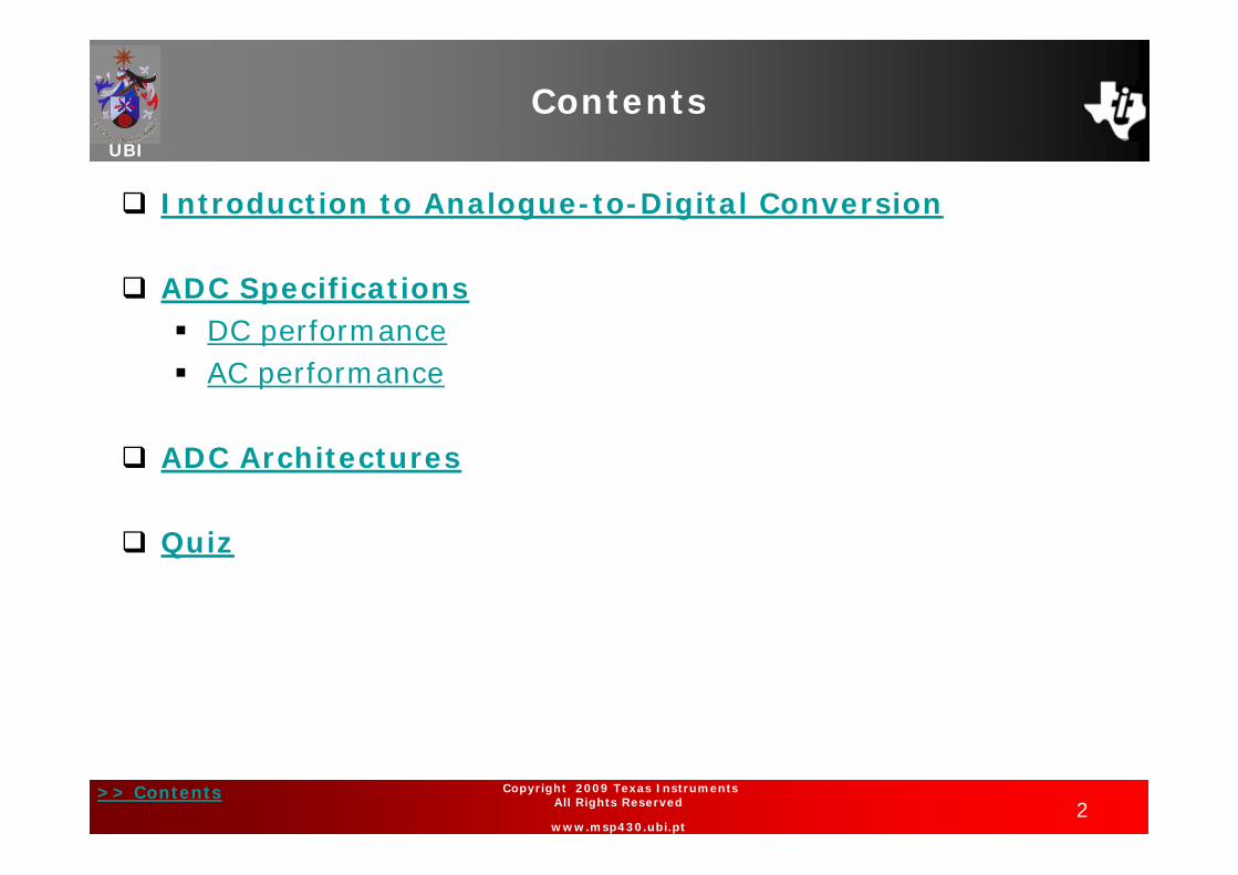
There are sufficient analogue peripherals in a number ofMSP430 family devices to realize a complete signalMSP430 family devices to realize a complete signalchain;
Analogue class of applications: Is more or less defined by bandwidth range; Require an established resolution range.
>> Contents4
Copyright 2009 Texas Instruments All Rights Reserved
www.msp430.ubi.pt

ADC Specifications (1/3)UBI
Resolution, R: The smallest change to the analogue voltage that can beThe smallest change to the analogue voltage that can be
converted into a digital code;
Th L Si ifi Bi (LSB) 1 The Least Significant Bit (LSB):n
R21
The resolution only specifies the width of the digital outputword, not the performance;
Most MSP430 devices offer a high-precision ADC:Slope;– Slope;
– 10, 12 or 14 Bit SAR;– 16 Bit Sigma-Delta.
>> Contents5
Copyright 2009 Texas Instruments All Rights Reserved
www.msp430.ubi.pt
g

ADC Specifications (2/3)UBI
Accuracy: Degree of conformity of a digital code representing theDegree of conformity of a digital code representing the
analogue voltage to its actual (true) value; Can express as the “degree of truth”.
>> Contents6
Copyright 2009 Texas Instruments All Rights Reserved
www.msp430.ubi.pt
ADC Specifications (3/3)UBI
Performance: Depends on the following specifications:Depends on the following specifications:
• Speed;• Accuracy, also depends on the circuitry type:
– DC:» Differential Non-Linearity (DNL);» Integral Non Linearity (INL);» Integral Non-Linearity (INL);» Offset error,» Gain error…
– AC:» Signal-to-noise ratio (SNR);» Signal-to-noise and distortion ratio (SINAD);» Total harmonic distortion (THD);» Spurious free dynamic range (SFDR)
>> Contents7
Copyright 2009 Texas Instruments All Rights Reserved
www.msp430.ubi.pt
» Spurious-free dynamic range (SFDR)…

ADC Specifications – DC performance (1/9)UBI
Differential Non-Linearity (DNL): Determines how far an output code is from a neighbouring Determines how far an output code is from a neighbouring
output code. The distance is measured as a VIN converted to LSBs;
No DNL error requires that:• as the VIN is swept over itsIN p
range, all output codecombinations will appearat the converter output;
DNL error < ± 1 LSB DNL error < ± 1 LSBensures no missing codes.
>> Contents8
Copyright 2009 Texas Instruments All Rights Reserved
www.msp430.ubi.pt
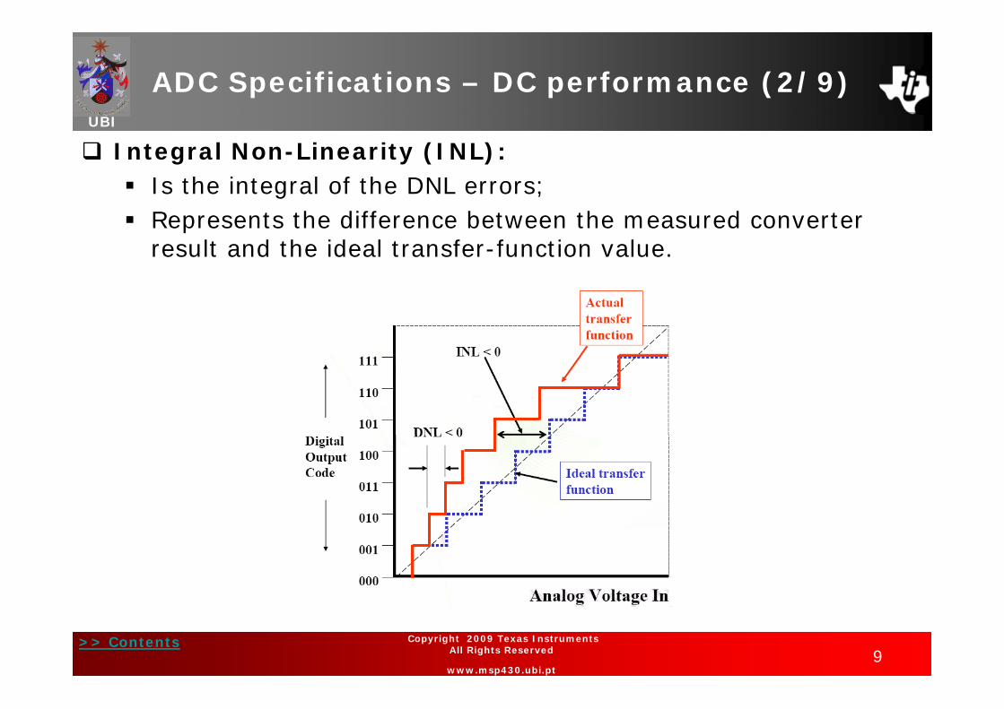
ADC Specifications – DC performance (2/9)UBI
Integral Non-Linearity (INL): Is the integral of the DNL errors;Is the integral of the DNL errors; Represents the difference between the measured converter
result and the ideal transfer-function value.
>> Contents9
Copyright 2009 Texas Instruments All Rights Reserved
www.msp430.ubi.pt
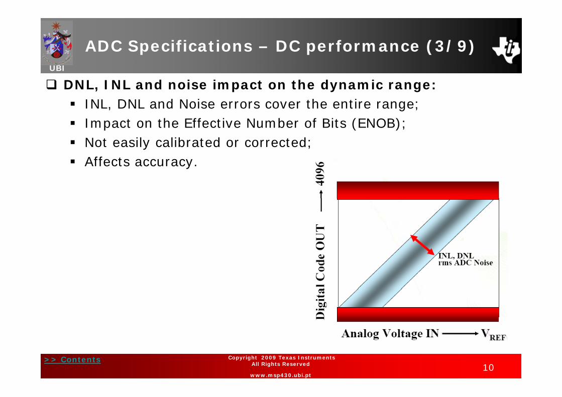
ADC Specifications – DC performance (3/9)UBI
DNL, INL and noise impact on the dynamic range: INL, DNL and Noise errors cover the entire range;INL, DNL and Noise errors cover the entire range; Impact on the Effective Number of Bits (ENOB); Not easily calibrated or corrected; Affects accuracy.
>> Contents10
Copyright 2009 Texas Instruments All Rights Reserved
www.msp430.ubi.pt

ADC Specifications – DC performance (4/9)UBI
Offset error: In bipolar systems, the offset error shifts the transfer function In bipolar systems, the offset error shifts the transfer function
but does not reduce the number of available codes.
>> Contents11
Copyright 2009 Texas Instruments All Rights Reserved
www.msp430.ubi.pt
ADC Specifications – DC performance (5/9)UBI
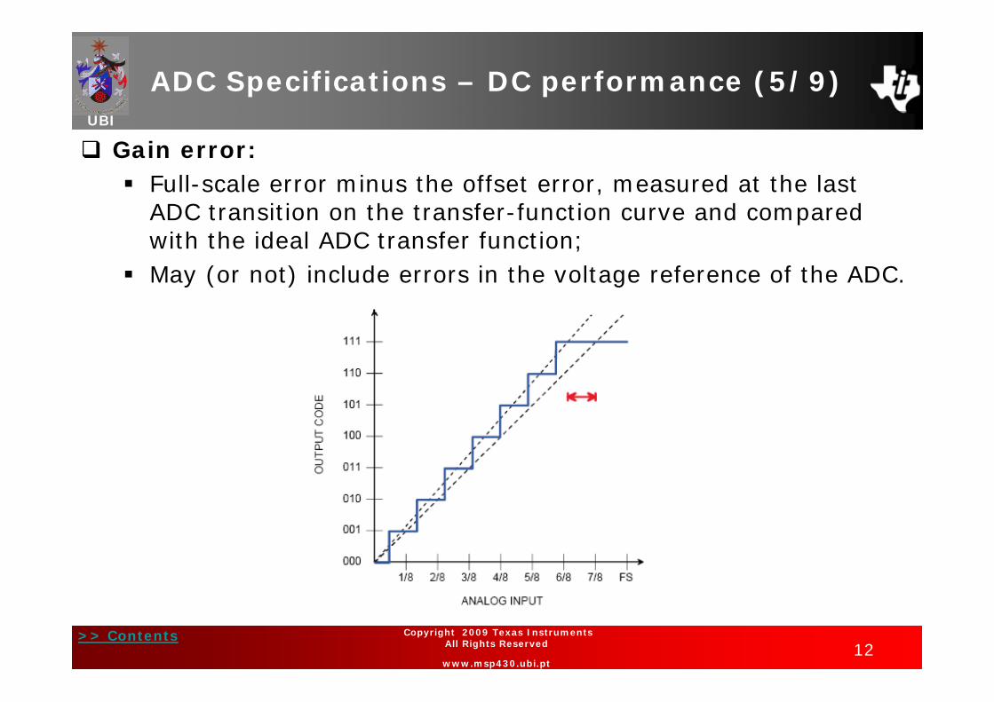
Gain error: Full-scale error minus the offset error, measured at the last Full scale error minus the offset error, measured at the last
ADC transition on the transfer-function curve and compared with the ideal ADC transfer function;
May (or not) include errors in the voltage reference of the ADC May (or not) include errors in the voltage reference of the ADC.
>> Contents12
Copyright 2009 Texas Instruments All Rights Reserved
www.msp430.ubi.pt
ADC Specifications – DC performance (6/9)UBI
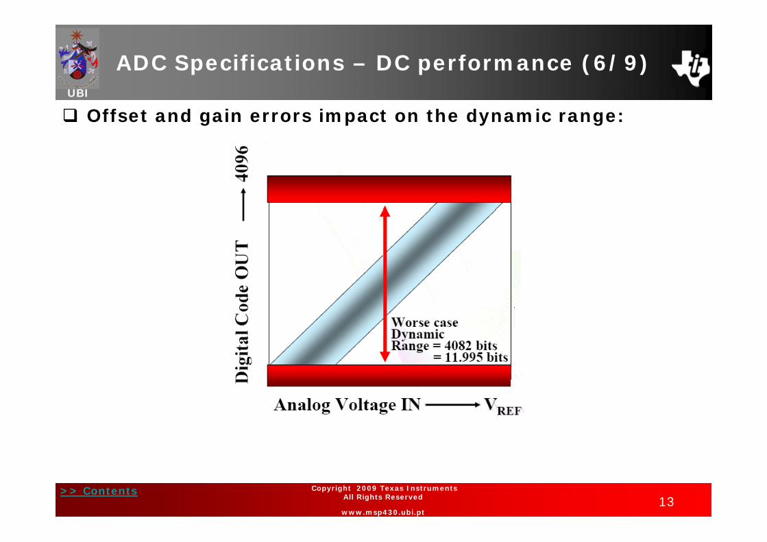
Offset and gain errors impact on the dynamic range:
>> Contents13
Copyright 2009 Texas Instruments All Rights Reserved
www.msp430.ubi.pt

ADC Specifications – DC performance (7/9)UBI
Offset (a) and gain (b) errors calibration:
Bipolar systems:• Shift the analogue input (x) and digital output (y) axes of
the transfer function so that the negative full-scale point the transfer function so that the negative full scale point aligns with the zero point:
y = a + (1+b) xy = a + (1+b) x
• Apply zero volts to the ADC input and perform a conversion. The conversion result represents the bipolar zero offset error. Perform a gain adjustment.
>> Contents14
Copyright 2009 Texas Instruments All Rights Reserved
www.msp430.ubi.pt

ADC Specifications – DC performance (8/9)UBI
Offset (a) and gain (b) errors calibration:
Unipolar systems:• Previous methodology is applicable if the offset is positive;
• Gain error can be corrected by software considering a linear function in terms of the ideal transfer function slope (m1) and measured (m ):and measured (m2):y = (m1/m2) x
Both offset and gain errors reduction techniques will imply partial loss of the ADC range.
>> Contents15
Copyright 2009 Texas Instruments All Rights Reserved
www.msp430.ubi.pt

ADC Specifications – DC performance (9/9)UBI
Code-Edge Noise: Amount of noise that appears right at a code transition of the transfer function;
Voltage Reference (internal or external): Besides the settling time the source of the reference voltage errors is settling time, the source of the reference voltage errors is related to the following specifications: Temperature drift: Affects the performance of an ADC converter
based on resolution; Voltage noise: Specified as either an RMS value or a peak-to-
peak value;peak value; Load regulation: Current drawn by other components will
affect the voltage reference; Temperature effects (offset drift and gain drift).
>> Contents16
Copyright 2008 Texas Instruments All Rights Reserved
www.msp430.ubi.pt

ADC Specifications – AC performance (1/6)UBI
AC parameters: Harmonics occur at multiples of the input frequency:
>> Contents17
Copyright 2009 Texas Instruments All Rights Reserved
www.msp430.ubi.pt
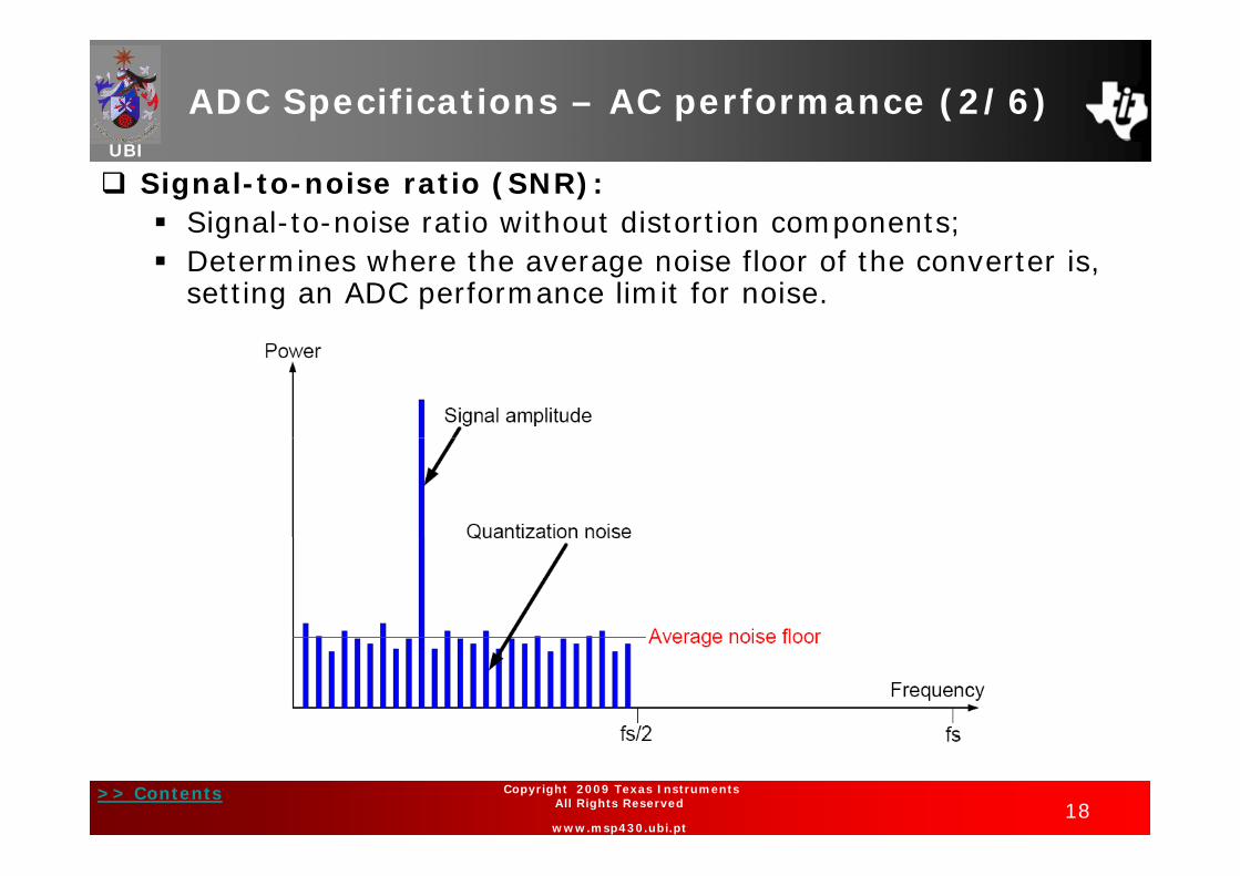
ADC Specifications – AC performance (2/6)UBI
Signal-to-noise ratio (SNR): Signal-to-noise ratio without distortion components; Determines where the average noise floor of the converter is,
setting an ADC performance limit for noise.
>> Contents18
Copyright 2009 Texas Instruments All Rights Reserved
www.msp430.ubi.pt
ADC Specifications – AC performance (3/6)UBI
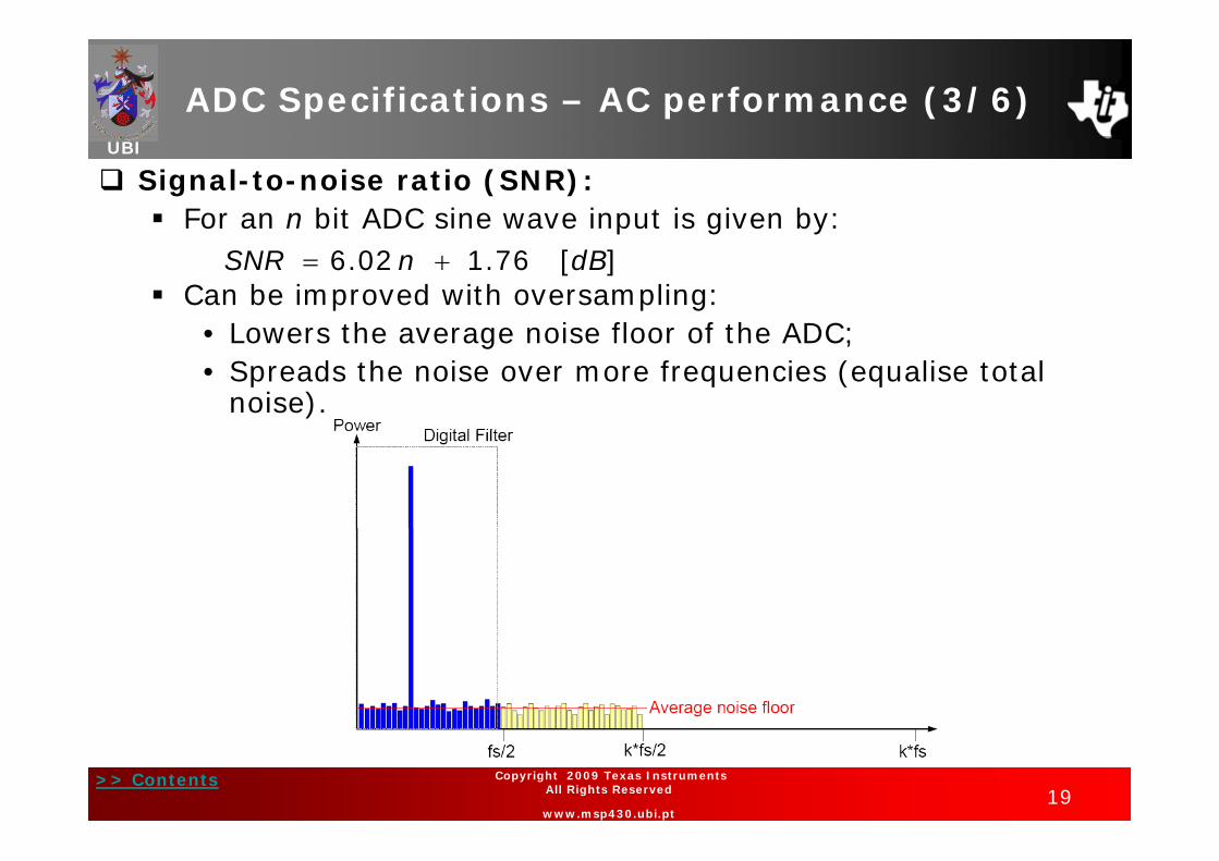
Signal-to-noise ratio (SNR): For an n bit ADC sine wave input is given by:
Can be improved with oversampling:• Lowers the average noise floor of the ADC;
][76.102.6 dBnSNR
• Lowers the average noise floor of the ADC;• Spreads the noise over more frequencies (equalise total
noise).
>> Contents19
Copyright 2009 Texas Instruments All Rights Reserved
www.msp430.ubi.pt

ADC Specifications – AC performance (4/6)UBI
Signal-to-noise ratio (SNR): Oversampling an ADC is a common principle to increase
resolution;
It reduces the noise at any one frequency point.It reduces the noise at any one frequency point.
A 2x oversampling reduces the noise floor by 3 dB, whichcorresponds to a ½ bit resolution increase;corresponds to a ½ bit resolution increase;
Oversampling by k times provides a SNR given by:
][log10761026 dBfnSNR s
][2
log1076.102.6max
10 dBf
nSNR
>> Contents20
Copyright 2009 Texas Instruments All Rights Reserved
www.msp430.ubi.pt

ADC Specifications – AC performance (5/6)UBI
Signal-to-noise and distortion ratio (SINAD): Similar to SNR;
Includes the harmonic content [total harmonic distortion], from DC to the Nyquist frequency;DC to the Nyquist frequency;
Is defined as the ratio of the RMS value of an input sine wave to the RMS value of the noise of the converter;to the RMS value of the noise of the converter;
Writing the equation in terms of n, provides the number of bits that are obtained as a function of the RMS noise (effective number of bits, ENOB):
02.6/76.1 SINADn
>> Contents21
Copyright 2009 Texas Instruments All Rights Reserved
www.msp430.ubi.pt

ADC Specifications – AC performance (6/6)UBI
Total harmonic distortion (THD): Gets increasingly worse as the input frequency increases;
Primary reason for ENOB degradation with frequency is that SINAD decreases as the frequency increases toward the Nyquist SINAD decreases as the frequency increases toward the Nyquist limit, SINAD decreases.
Spurious-free dynamic range (SFDR): Defined as the ratio of the RMS value of an input sine wave to
the RMS value of the largest trace observed in the frequency domain using a FFT plot;
If the distortion component is much larger than the signal of interest, the ADC will not convert small input signals, thus limiting its dynamic range.
>> Contents22
Copyright 2009 Texas Instruments All Rights Reserved
www.msp430.ubi.pt
g y g

ADC Architectures (1/4)UBI
There are many different ADC architectures: Successive Approximation (SAR); Sigma Delta (SD or ); Slope or Dual Slope; Pipeline; Pipeline; Flash...as in quick, not memory.
>> Contents23
Copyright 2009 Texas Instruments All Rights Reserved
www.msp430.ubi.pt

ADC Architectures (2/4)UBI
The selection of an MSP430 ADC will depend on: Voltage range to be measured; Maximum frequency for AIN; Minimum resolution needed vs. analogue input variation; The need for differential inputs; The need for differential inputs; Voltage reference range; The need for multiple channels for different analogue inputs.
ADC architecture
Resolution Conversion rate
Advantages Disadvantages
Zero-cycle latency Low latency-time
SAR 18 bit < 5 Msps Low latency time High accuracy Low power Simple operation
Sample rates 2-5 MHz
High resolution
SD 24 bit 16-18 bit
< 625 ksps < 10 Msps
High stability Low power Moderate cost
Cycle-latency Low speed
Pi li 16 bi 500 M Higher speeds Lower resolution D l /D l
>> Contents24
Copyright 2009 Texas Instruments All Rights Reserved
www.msp430.ubi.pt
Pipeline 16 bit < 500 Msps Higher speeds Higher bandwidth Delay/Data latency
Power requirements
ADC Architectures (3/4)UBI
ADC architectures included in the MSP430 devices ADC architectures included in the MSP430 devices populated in the hardware development tools: 10 Bit SAR: MSP430F2274 eZ430-RF2500;
12 Bit SAR: MSP430FG4618 Experimenter’s board;
16 Bit Sigma-Delta: MSP430F2013 eZ430-F2013 and Experimenter’s board.
>> Contents25
Copyright 2009 Texas Instruments All Rights Reserved
www.msp430.ubi.pt
ADC Architectures (4/4)UBI
Further information concerning ADC fundamentals and applications can found on the TI website: Introduction to MSP430 ADCs <slap115.pdf> Understanding Data Converters <slaa013.pdf> A Glossary of Analogue-to-Digital Specifications and A Glossary of Analogue to Digital Specifications and
Performance Characteristics <sbaa147a.pdf> Optimized Digital Filtering for the MSP430 <slap108.pdf> Efficient MSP430 Code Synthesis for an FIR Filter Efficient MSP430 Code Synthesis for an FIR Filter
<slaa357.pdf> Working with ADCs, OAs and the MSP430 <slap123.pdf> Hands-On: Using MSP430 Embedded Op Amps <slap118.pdf> Oversampling the ADC12 for Higher Resolution <slaa323.pdf> Hands-on Realizing the MSP430 Signal Chain through ADPCM Hands on Realizing the MSP430 Signal Chain through ADPCM
<slap122.pdf> Amplifiers and Bits: An Introduction to Selecting Amplifiers for
Data Converters <sloa035b pdf>
>> Contents26
Copyright 2009 Texas Instruments All Rights Reserved
www.msp430.ubi.pt
Data Converters <sloa035b.pdf>

Quiz (1/3)UBI
9. The performance of an ADC is expressed by which specifications:(a) Speed, Accuracy, Signal-to-noise ratio (SNR) and distortion
ratio (SINAD);(b) Offset and gain errors and Signal to noise ratio (SNR);(b) Offset and gain errors, and Signal-to-noise ratio (SNR);(c) Integral (INL) and Differential Non-Linearities (DNL) and Total
harmonic distortion (THD);(d) All of the above.
10 O li 10. Oversampling means:(a) An ADC performance parameter to limit noise;(b) Sampling at a rate much higher than the signal of interest;(b) Sampling at a rate much higher than the signal of interest;(c) To increase the resolution;(d) All of the above.
>> Contents27
Copyright 2009 Texas Instruments All Rights Reserved
www.msp430.ubi.pt
Quiz (2/3)UBI
11. A low cost, low power consuming application that requires a 12 bit resolution with a 100 Hz output data rate should use an ADC with the architecture:(a) Slope;(b) Sigma Delta;(b) Sigma-Delta;(c) SAR;(d) Flash.( )
>> Contents28
Copyright 2009 Texas Instruments All Rights Reserved
www.msp430.ubi.pt

Quiz (3/3)UBI
Answers:9. (d) All of the above.
10. (d) All of the above.
11. (a) Slope.
>> Contents29
Copyright 2009 Texas Instruments All Rights Reserved
www.msp430.ubi.pt