Embed Size (px)
Citation preview
Typical Attack Techniques for Compromising Point of Sale PIN Entry Devices
Physical Security Testing Workshop
Steven Bowles, Project Manager Payment Assurance
Electronic Warfare Associates - Canada
27 September 2005
Who Are We?Who Are We?
• Payment Assurance Lab– Interac Device Certification Agent– PCI Test Lab (in process of accreditation)
• ITSET Lab– Common Criteria– FIPS 140– FIPS 201
• Other Computer Security Consulting Services
OverviewOverview
• Introduction• Threat Agent Goals• Typical Vulnerabilities in PoS PEDs
– Identifying & Exploiting Weaknesses– Tools & Techniques
• Design Considerations to Mitigate the Risk
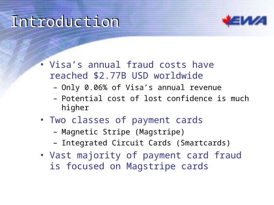
IntroductionIntroduction
• Visa’s annual fraud costs have reached $2.77B USD worldwide– Only 0.06% of Visa’s annual revenue– Potential cost of lost confidence is much higher
• Two classes of payment cards– Magnetic Stripe (Magstripe)– Integrated Circuit Cards (Smartcards)
• Vast majority of payment card fraud is focused on Magstripe cards

Threat Agent GoalsThreat Agent Goals
Threat Agent GoalsThreat Agent Goals
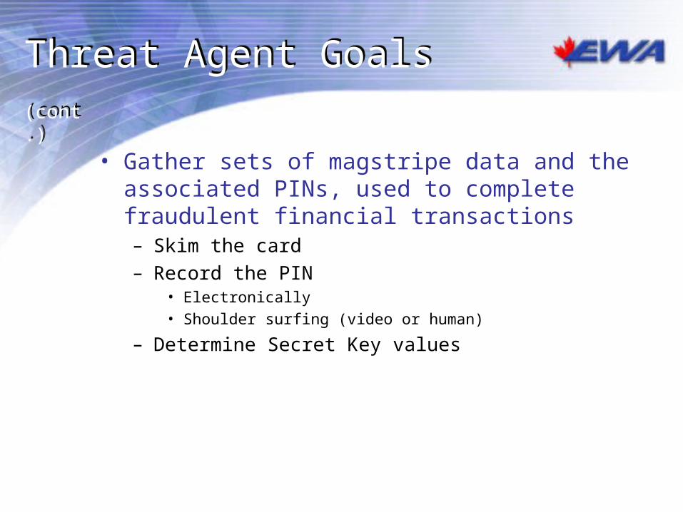
• Gather sets of magstripe data and the associated PINs, used to complete fraudulent financial transactions– Skim the card– Record the PIN
• Electronically• Shoulder surfing (video or human)
– Determine Secret Key values
(cont.)(cont.)
Typical VulnerabilitiesTypical Vulnerabilities
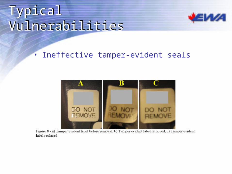
• Ineffective tamper-evident seals
Typical VulnerabilitiesTypical Vulnerabilities
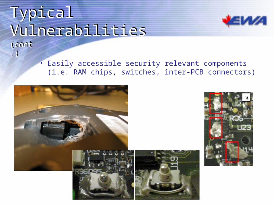
• Easily accessible security relevant components (i.e. RAM chips, switches, inter-PCB connectors)
(cont.)(cont.)
Typical VulnerabilitiesTypical Vulnerabilities
• Openings that can be used to conceal penetration attempts or malicious circuitry
(cont.)(cont.)
Typical VulnerabilitiesTypical Vulnerabilities
• Surface mounted display covers attached with weak glues or epoxies
(cont.)(cont.)
Typical VulnerabilitiesTypical Vulnerabilities
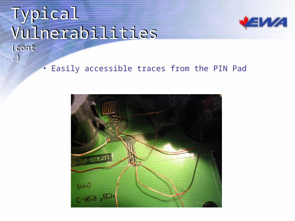
• Easily accessible traces from the PIN Pad
(cont.)(cont.)
Typical VulnerabilitiesTypical Vulnerabilities
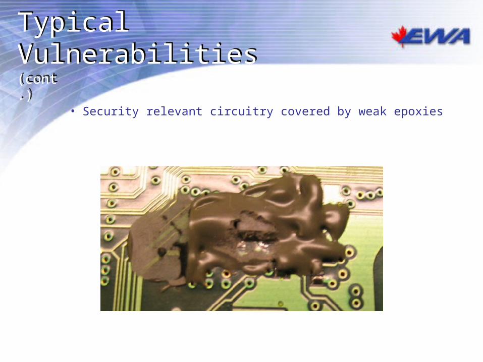
• Security relevant circuitry covered by weak epoxies
(cont.)(cont.)
Identifying & Exploiting WeaknessesIdentifying & Exploiting Weaknesses
• Conduct an attack by:– Defeat passive tamper response mechanisms– Disable or bypass any relevant active tamper response
mechanisms– Intercept key entry information from PIN Pad– Determine cryptographic keys (if necessary)

Identifying & Exploiting WeaknessesIdentifying & Exploiting Weaknesses
• PED Attack Methodology1. Enumeration of a PEDs sensitive components and
physical safeguards to aid in planning an attack;
2. Gaining Access allows for the proving, refinement, and packaging of a theoretical attack;
3. Exploiting a PED with the developed attack vector to record sensitive data; and
4. Covering Tracks by effectively hiding the malicious modifications.
(cont.)(cont.)
• Enumeration– Identify components and PCB traces that could provide
access to sensitive information;– Determine where the active tamper detection sensors are,
what they protect, and how they trigger;– Determine if tamper detection mechanisms can be
disabled or bypassed from openings in the device;– Find any areas that can be cut into and covered up;
• make sure that the cuts won’t trigger a tamper response. • evaluate whether or not it is possible to disable any or all tamper
response mechanisms from these cuts; and
– Determine if any cuts or openings allow access to security relevant traces or components (i.e. PIN Pad traces).
Identifying & Exploiting WeaknessesIdentifying & Exploiting Weaknesses(cont.)(cont.)
• Gaining Access– a procedure must be developed and refined such that the
exploit can be executed economically and efficiently• (according to PCI; $25k USD and 10 hrs.).
– also include the development of any specialized tools or circuitry required to gain access to the sensitive data once exposed.
Identifying & Exploiting WeaknessesIdentifying & Exploiting Weaknesses(cont.)(cont.)
• Exploiting– It must be possible to insert the required malicious
hardware and/or software needed to monitor or record the targeted sensitive data
– Depending on the complexity of the attack, a Threat Agent may require a significant amount of practice to refine the technique
– Retries of this nature can be frustrated if the PED enters into a severe non-operational state once the tamper response mechanisms have been triggered.
• won’t remain powered-up without the entry of authenticated keys or a password)
Identifying & Exploiting WeaknessesIdentifying & Exploiting Weaknesses(cont.)(cont.)
• Covering Tracks– Acquisition of cardholder data requires the participation of
a non-colluding user– It must be possible to reassemble a compromised PED
with original or replacement parts such that the exploit is not noticeable to the casual observer.
• if an exploit is making use of an opening under a removable cover, where the opening needs to be widened, care should be taken to ensure that a edge is left that can be used for reattaching the display cover once the exploit has been implemented.
Identifying & Exploiting WeaknessesIdentifying & Exploiting Weaknesses(cont.)(cont.)
Tools & TechniquesTools & Techniques
• Hand-held Rotary Tool– access internal areas by cutting the case– removing internal case material in order to access
security relevant components– for the removal of large/hard epoxies
• Adhesives– hold switches shut– hold other pieces in place
• Magnet Wire– Can be sharpened and inserted into small conductive vias
on a PCB
Tools & TechniquesTools & Techniques
• Dental Pick– scraping epoxies from components or conductive vias– applying adhesives to keep tamper response switches
closed– with a small amount of epoxy, can be used to place
malicious wires and components into tight spaces.
• Conductive Epoxy– short out component contacts – act as a ‘cold weld’ for heat sensitive applications and
tight areas. – easy method of attaching wires to traces that have been
revealed by scrapping off the PCB’s conformal coating.
(cont.)(cont.)

Design Considerations to Mitigate the RiskDesign Considerations to Mitigate the Risk
Design Considerations to Mitigate the RiskDesign Considerations to Mitigate the Risk
• Run keypad/active tamper response mechanism traces on the middle layer(s) of a PCB;
• Place keypad/active tamper response mechanism vias in inaccessible areas;
• Keep active tamper response mechanisms independent of each other as long as possible;
• Try to place active tamper response traces and chip pins away from traces and chip pins that carry a signal similar to the ‘NO TAMPER DETECTED’ signals;
(cont.)(cont.)
Design Considerations to Mitigate the RiskDesign Considerations to Mitigate the Risk
• Ensure that items on, or in the device, that are not meant to be removed, cannot be removed without triggering a tamper response mechanism;
• Do not rely only on passive mechanisms such as epoxy or tamper evident seals/labels;
• Avoid placing removable covers on the device;• Design the device so that every aspect of the
device increases the security of the device;• Do not allow physical access to the internals of the
device for any reason.
(cont.)(cont.)
Design Considerations to Mitigate the RiskDesign Considerations to Mitigate the Risk
• Do not allow the device to be reset and/or reused after a physical attack has been attempted.
• Design active tamper response mechanisms that use conductive pucks to require a constant pressure applied to them to be effective; and
• Use tamper detection switches that are small and require a fair amount of pressure to keep the switch closed.
(cont.)(cont.)

In ClosingIn Closing
Physical Security alone will never guarantee the security of our
Systems.

QuestionsQuestions
Steven Bowles
Project Manager Payment Assurance
EWA-Canada
(613)230-6067 x1221
http://www.ewa-canada.com
Mahalo!