Embed Size (px)
Citation preview

~-------- -
OPERATING INSTRUCTIONS
TYPE 1150·A
DIGITAL FREQUENCY METER
GENERAL RADIO COMPANY
B
...... ...... 01 0
I
l>

O·PERATING INSTRUCTIONS
TYPE 1150·A
DIGITAL FREQUENCY METER
Form 1150-0100-B October, 1963
Copyright 1962 by General Radio Company West Concord, Massachusetts, USA
GENERAL R A D I 0 COMPANY WEST CONCORD, MASSACHUSETTS, USA

Figure 1-1. Panel view of the Type 1150-A Digital Frequency Meter.
SPECIFICATIONS
Frequency Range: 10 cps to 300 kc. Input Impedance: AC-coupled; approximately 0.5 megohm shunted by less than 100 pf. Sensitivity: Better than 1 volt, peak-to-peak; for pulse input, duty ra~i? should be·_between 0.2 aJ?d 0.8. For input pulses of higher than m1mmum amphtudc, duty ratiO becomes less important. Display: 5-digit, in-line Numerik register, incandescent-lamp operated. Display Time: Adjustable from 0.5 to 5 seconds, or infinity. Counting Interval: 0.1, 1, or 10 seconds, or can be set manually. Accuracy : ± 1 count ±crystal-oscillator stability: Crystal-Oscillator Stability
Short-Term: Better than 71! part per million. Cycling: Less than counter resolution. Temperature Effects: Less than 271! parts per million for rise -of 0 to 50 C ambient. Wannup: Within 1 part per million after 15 minutes.
Patent Applied For.
Aging: Less than 1 part per million per week after four weeks decreasing thereafter. '
Cr:rs.tai·Frequency Adjustment: The frequency is within 10 parts per m1lhon of 100 kc when shtpped. Frequency adjustment provided. Power Requirements: 105 to 125 (or 210 to 250) volts, 50 to 60 cps, 45 watts. Accessories Supplied: TYPE CAP-22 Power Cord eight replacement incandescent lamps, spare fuses. ' Accessories Available: TYPE 1136-A Digital-to-Analog Converter (page 99) and TYPE 1137-A Data Printer (page 100) operate from output of TYPE 1150-AP model. Cabinet: Rack-bench (see page 210). Dimensions: Bench model - width 19, height 3% depth 12 71! inches (485 by 99 by 320 mm), over-all; rack model- panel 19 by 371! mches (485 by 90 mm); depth behind panel 12%' inches (325 mm). Net Weight: 171/z pounds (8 kg). Shipping Weight: 20 pounds (9.5 kg).
General Radio Experimenter reference, Vol 36, No. 4, April 1962

INTRODUCTION· OPERATING PROCEDURE
SECTION 1 INTRODUCTION
The Type 1150-A Digital FrequencyMeter(see Figure 1-1) is a general-purpose, basic, digital counter for measuring, setting, and monitoring frequencies, for counting random events, and for industrial counting applications. Among its many frequency measurement applications are the test, adjustment, and calibration of oscillators, telemetering equipment, i-f amplifiers and filters (crystal, mechanical, and magnetostrictive). This frequency meter measures frequencies between 10 cps and 220 kc with a precision of ±0.1 cps.
SECTION 2 OPERATING
2.1 CONTROLS AND CONNECTORS.
With appropriate transducers, it can be used to measure such physical quantities as pressure, temperature, strain, and weight. In conjunction with an optical or magnetic pickup, it will measure rotational speed.
Other important applications in industry include the counting of units on a production line and other nonperiodic events.
It can be started, stopped, and cleared by external signals, so that it can be used as part of a larger system.
PROCEDURE
The following table lists the controls and connectors on the Type 1150-A Digital Frequency Meter:
INPUT
~ @
The INPUT binding-post terminals are for connection of the signal to be measured. The lower (ground) terminal is connected directly to the metal case of the instrument.

.. TYPE 1150-A DIG IT AL FREQUENCY METER
2
DISPLAY TIME
(@j" • oo
CHECK
0
0 COUNTING
COUNTING TIME SEC 1.0 10
O.I®MA'"AL
START-STOP
0
POWER
OFF
Clockwise rotation of the DISPLAY TIME control increases the time interval for display of the measurement result. The approximate range of display time is one-half to five seconds; the one-second setting is indicated. Rotating the knob fully clockwise activates a switch that gives continuous display(ooposition) until the RESET button is pressed .
The latching-type, pushbutton CHECK switch is activated when the switch is pressed toward the panel and then released. The two positions, one closer to the panel than the other, are indicated by the length of shaft exposed. The position closer to the panel is the normal position for measurement of an input signal. The position farther out from the panel is for self-check operation of the instrument with the internal 100-kc signal connected across the INPUT terminals.
The COUNTING lamp lights while the instrument is measuring and is off during the display and reset intervals. The lamp functions for both automatic and manual operation.
The four positions of the COUNTING TIME SEC control select the time interval for which the input signal is sampled (counted). In the 0.1 position, the sampling interval is 0.1 second and the indicator reads in 10-cycle units; in the 1.0 position, the input is sampled for one second and the indicator reads in cycle-per-second units; the 10 position gives a 10-second sampling interval and a display in 0.1-cycle units;/ in the MANUAL position, the sampling interval is controlled by the START-STOP switch.
The latching-type, pushbutton START-STOP switch is activated when the switch is pressed toward the panel and then released. The two positions, one closer to the panel than the other, are indicated by the length of shaft exposed. When the COUNTING TIME SEC control is in the MANUAL position, this START-STOP switch controls the time that the input signal is sampled. The sampling interval starts when the switch is set in the position farther out from the panel and stops when the switch is put in the position closer to the panel.
The POWER switch interrupts the 115 volts supplied to the fan motor and the instrument de supply. As long as the instrument is plugged in, the primary and secondary windings of the power transformer are energized to keep the crystal oven at its proper temperature. Note that line voltage and other voltages are present with power "off".

RESET
@
105-125V 50-60C
(@) INT IOOKC
INT
TIMED BASEW
EXT
EXT (@) IOOKC@ INPUT
~ PHOTO
ELECTRIC PICKOFF
OPERATING PROCEDURE
When the nonlatching, pushbutton RESET switch is pressed momentarily, the display interval or the counting interval is interrupted and a new count is initiated.
Power-input socket accepts the power cord provided. Instruments are normally supplied for operation from 105 to 125 volts. The power transformer can be reconnected for operation from 210 to 250 volts (refer to Section 2.2.4).
The internally generated, 100-kc reference signal is available at the jack labeled INT 100 KC.
With the TIME BASE slide switch in the INT position, the reference signal is taken from an internal stable crystal oscillator. With the TIME BASE slide switch in the EXT position, an external 100-kc signal should be applied to the lower phone jack. When no external reference is connected, the slide switch should be in the INT position. Operation without an external reference signal and with the switch at EXT will yield incorrect measurements.
The lower phone jack, EXT 100 KC INPUT, is for connection of an external 100-kc reference signal.
The six -pin AUX plug is to connect the instrument to auxiliary equipment (refer to Section 2.6.3),
The three-connector PHOTOELECTRIC PICKOFF telephone jack is for direct connection of an optical transducer (refer to Section 2.6.2).
3
~--T~Y~P=E~1~15~0-~A~D~I~G~IT~A~L~F~R~EQ~U~E~N~C~Y~M~E~T~E~R---------------------------
c
1.-
c
2.2 INSTALLATION.
2.2.1 INSTRUMENT LOCATION. To cool the internal components, air is vented through an air filter at the rear to an exhaust fan on the left-hand side of the instrument. The frequency meter must be mounted so that air flow is not blocked at either the filter or the exhaust port. The instrument will operate properly in any orientation.
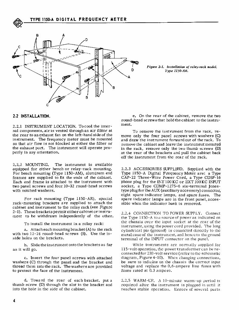
2.2.2 MOUNTING. The instrument is available equipped for either bench or relay-rack mounting. For bench mounting (Type ll50-AM), aluminum end frames are supplied to fit the ends of the cabi:aet. Each end frame is attached to the instrument with two panel screws and four 10-32 round-head screws with notched washers.
For rack mounting (Type ll50-AR}, special rack-mounting brackets are supplied to attach the cabinet and instrument to the relay rack (see Figure 2-1). These brackets permit either cabinet or instrument to be withdrawn independently of the other.
To install the instrument in a relay rack:
a. Attach each mounting bracket (A) to the rack with two 12-24 round-head screws (B). Use the inside holes on the brackets.
b. Slide the instrument onto the brackets as far as it will go.
c. Insert the four panel screws with attached washers (C) through the panel and the bracket and thread them into the rack. The washers are provided to protect the face of the instrument.
d. Toward the rear of each bracket, put a thumb screw (D) through the slot in the bracket and into the hole in the side of the cabinet.
4
-(Q 0
A
Figure 2-1. Installation of relay-rack model, Type 1150-AR.
e. On the rear of the cabinet, remove the two round-head screws that hold the cabinet to the instrument.
To remove the instrument from the rae!<, remove only the four panel screws with washers (C) and draw the instrument forward out of the rack. To remove the cabinet and leave the instrument mounted in the rack, remove only the two thumb screws (D) at the rear of the brackets and pull the cabinet back off the instrument from the rear of the rack.
2.2.3 ACCESSORIES SUPPLIED. Supplied with the Type 1150-A Digital Frequency Meter are: a Type CAP-22 Three-Wire Power Cord, a Type CDSP-16 phone plug for the INT 100 KC or EXT 100 KC INPUT socket, a Type CDMP-1275-6 six-terminal Jonestype plug for the AUX (auxiliary accessory) connector, eight spare indicator lamps, and spare fuses. The spare indicator lamps are in the front panel, accessible when the indicator bank is removed.
2.2.4 CONNECTION TO POWER SUPPLY. Connect the Type 1150-A toasourceofpoweras indicated on the chassis over the input socket at the rear of the instrument, using the power cord provided. The long cylindrical pin (ground) is connected directly to the metal. case of the instrument, and hence to the ground terminal of the INPUT connector on the panel.
While instruments are normally supplied for 115-volt operation, the power transformer can be reconnected for 230 -volt service (refer to the schematic diagram, Figure 4-10). When changing connections, be sure to indicate on the chassis the correct input voltage and replace the 0.6-ampere line fuses with fuses rated at 0.3 ampere.
2.2.5 WARM-UP. A 10-minute warm-up period is required after the instrument is plugged in until it reaches stable operation. Errors of several parts

per million in frequency measurement may. occur during warm -up. The crystal oven for the internal reference oscillator will then remain at the proper operating temperature as long as the instrument is plugged "in, regardless of the setting of the POWER switch.
2.2.6 CHECK FOR PROPER OPERATION. Set the rear TIME BASE control to INT, the POWER switch to POWER, and allow a few seconds for the instrument to attain stable operation. Set the COUNTING TIME control to 0.1 SEC, the DISPLAY TIME control to approximately 1 SEC, and set the CHECK and the START-STOP pushbuttons so they are in the position farther out from the panel. The instrument should display 10000 (100 kc) for one second, clear to zero, count again, etc.
With the COUNTING TIME control set to 1.0 or 10, the meter should still measure the frequency within one count. The display will be 00000 because of the change in sampling time.
2.2. 7 APPLYING AN INPUT SIGNAL. Apply the signal to be measured at the INPUT binding posts on the panel. The lower terminal (ground) is connected to the metal case of the instrument and to the ground connection of the three-wire power cord.
VOLTAGE
INPUT VOLTAGE
REFERENCE
~~----~~----~------~--~~~VOLTA&
Figure 2-2. Input signal waveform showing points where counts are generated (x) and points where the input circuits reset (0).
The input circuits have a small voltage hysteresis, or backlash. They generate a count (points X in Figure 2- 2) every time the signal voltage exceeds the reference voltage by a small amount (approximately 0.2 volt). Before another count can be generated, the circuits must be reset (points 0 in Figure 2-2) by a decrease in input voltage to a value approximately 0.2 volt below the reference voltage. Because of this hysteretic action, an input voltage of at least 0.4 volt is necessary to generate counts. Since the reference voltage changes with temperature and some noise is always present, an input voltage of at least 1 volt peak-to-peak is specified for proper operation. The input signal is capacitively coupled to the input circuit, so that the reference voltage is approximately the average value of the input signal. The counts are generated when the input signal voltage is increasing (positive slope in Figure 2- 2).
OPERATING PROCEDURE
VOLTAGE
Figure 2-3. Example of an input signal waveform which could generate tw~ counts per cycle.
It is possible to have a waveform that will generate two counts per cycle, such as that shown in Figure 2-3. The input circuits cannot discriminate between the waveforms shown in Figures 2-2 and 2-3 so the frequency indicated for the signal shown in Figure 2-3 may be twice the actual value. To eliminate this type of error, reduce the amplitude of the input signal.
VOLTAGE
--n-- --1\._---i ~'~" ~-=v:=v~ "TIME
Figure 2-4. Example of an input signal waveform with noise which could cause a missing count.
If the input signal is very close in amplitude to the minimum amplitude for triggering , a slight amount of noise can cause a missing count and corresponding measurement error (see Figure 2-4).
Since the capacitive coupling of the input signal causes the input circuits to generate a count at the average value of the input voltage, a pulse-type input signal should have a duty ratio (ratio of pulse duration to period) between 0.2 and 0.8, depending on the amplitude of the pulse. For the pulse waveform shown in Figure 2-Sa, although the peak-to-peak amplitude may be several volts, the average voltage is not sufficient to reset the input circuits. This type of error cannot usually be eliminated by increasing
VOLTAGE
0+----H------------H---------------- TIME
,-- REFERENCE t-- - - - - 1- 1- - - - - - - LEVEL
Figure 2-5a. Pulse-type input signal with too low a duty ratio to generate a count.
5

~--T_Y_P_E_ll_S_O-_A_D_I_G_IT_A_L __ F_R_E_Q_U_E_N_C_Y __ M_ET_E_R ____________________________ __
Figure 2-5b. Pulse-shaping circuit to change the waveform shown in Figure
2-5a.
the amplitude of the input signal without overloading the input circuits. It is possible, however, to measure the frequency of very low duty ratio signals by using an external circuit similar to the one shown in Figure 2-5b, which reshapes the waveform.
2.3 FREQUENCY MEASUREMENT.
2.3.1 GENERAL.
Set the COUNTING TIME control to the desired sampling interval; the longer the counting interval used, the greater the accuracy of measurement. (At 0.1 SEC, the meter will read in tens of cycles; at 1.0 SEC, the meter will read in qxcles per second; at 10 SEC, the meter will read in tenths of cycles per second.} The indicated frequency is the value averaged over the last counting interval.
Set the DISPLAY TIME control to a convenient display interval. (Range is approximately 0.5 to 5 seconds.) For easiest reading, set this control for minimum time between the end of the display interval and start of the next counting interval. This is particularly helpful when one-second counting interval is used.
To retain the displayed count, rotate the DISPLAY TIME control clockwise until the switch is activated (ooposition). The display will be held until the RESET button is pushed to reset the counting units to zero and initiate a new count.
2.3.2 MANUAL GATING FOR LOW-FREQUENCY SIGNALS. It is possible to generate accurate counting intervals longer than 10 seconds by use of the manualgatingfeature. This is especially useful for measurement oflow-frequency signals. For example, if a 20-cps signal is measured with 10-second samples, the indicator will read 200 counts and the possible onecount error amounts to ±0.5% of the measurement. If, however, a 100-second sampling time is used, the accuracy of the displayed 2000 is ±0.05%.
To use manual gating, set the START-STOP button in the outer position, and the COUNTING TIME control to 10 SEC. After the counting has started but before 10 seconds has elapsed, turn the COUNTING TIME control to MANUAL, which blocks the instrument so that counting will not stop. To stop the count, return the COUNTING TIME control to 10 SEC and
6
the counting will stop on the next multiple of 10 seconds. For example, for a 100-second sampling interval, return the COUNTING TIME control to 10 SEC between 90 and 100 seconds after the start of the counting.
2.4 MANUAL TOTALIZING OPERATION.
For counting or totalizing operations, set the COUNTING TIME control to MANUAL and use the START-STOP button to start (outer position) and stop (inner position) the count. The DISPLAY TIME control is effective during manual operation. The RESET button is also operative, but use of this control while the instrument is counting can lead to a false count, especially for high-frequency signals. To clear the indicators, stop the count with the START-STOP control and then reset.
2.5 USE OF AN EXTERNAL REFERENCE SOURCE.
An externa1100-kc signal can be used as a reference source in place of the 100-kc signal from the crystal oscillator of the Type ll50-A. Apply the signal to the EXT 100 KC INPUT phono jack at the rear of the instrument and set the TIME BASE switch to EXT. The external signal source should be capable of providing 0.3 volt across a 1-kilohm load.
2.6 CONNECTION TO ACCESSORY EQUIPMENT.
2.6.1 INTERNALOSCILLATORSIGNAL. At theiNT 100 KC phono jack on the rear of the instrument, a high-impedance output from the very stable 100-kc crystal oscillator is available for driving accessory equipment.
2~6.2 PHOTOELECTRIC PICKOFF. A three-terminal telephone jack is provided on the rear of the instrument for direct connection to a General Radio Type 1536-A Photoelectric Transducer. The transducer has a light source and a photoconductor which convert changes in reflection of the light source into electrical input signals. For instance, when the transducer is placed in the path of a piece of reflecting tape on a rotating object, the frequency meter indicates revolutions per second. The photoelectric pickoff signal is in parallel with the INPUT terminals, so, for proper operation with the pickoff, no signal should be connected to the INPUT terminals.
2.6.3 AUXILIARY EQUIPMENT. A six-connector Jones-type socket (AUX) at the rear of the instrument is provided for connection to auxiliary equipment. Table 2 -1li sts the signals available at this connector.

OPERATING PROCEDURE
TABLE 2-1 AUXILIARY CONNECTIONS
Pin Internal Signal
1 Ground
2 De power supply
3 Negative pulse from highest-unit indicator ("spill-over" signal).
4 Connection for exter-nally duplicating the RESET function
5 Connection for exter-nally duplicating the START-STOP function
6 Positive reset pulse output
TO PIN 2 2·7 k!l AUX,+20v~
TO PIN 4 • ( AUX
Output
0 volt.
+20 v regulated, with less than 0.5 v of high-frequency ripple while the instrument is operating. Supplies up to 100 rna; however, even an instantaneous short to ground will cause failure of the regulating transistor (Q501) and/or opening of the fuses.
The output transfer pulse from the decade driving the highest-unit indicator (one furthest to the left). Should be capacitively coupled, if used. Overload can cause errors in instrument operation and a direct short may lead to permanent damage.
See Figure 2-6.
See Figure 2-7.
+ 15 volts except for approximately 4 msec when the output is +20 volts while the indicators clear. Over-loading this terminal will cause instrument failure, and even a momentary direct short will cause perman-ent damage.
TO PIN 2 ---------, AUX -= )STOP TOPIN5~.n
A~; PIN I S~OT SWIT~ rsTART
AUX 4
Figure 2-6. External connections which duplicate the function of the RESET button. Momentarily closing the normally open
switch has the same effect as pressing the RESET button.
Figure 2· 7. External connections which duplicate the function of the START -STOP button. Resistor R243 should be disconnected from switch S201 when this modification is made.
7
~ TYPE 1150-A DIGITAL FREQUENCY METER ~--------------
SECTION 3 PRINCIPLES OF
3.1 GENERAL.
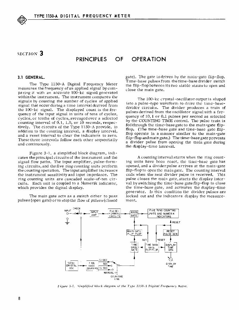
The Type 1150-A Digital Frequency Meter measures the frequency of an applied signal by comparing it with an accurate 100-kc signal generated within the instrument. The instrument compares the signals by counting the number of cycles of applied signal that occur during a time interval derived from the 100-kc signal. The displayed count is the frequency of the input signal in units of tens of cycles, cycles, or tenths of cycles, averaged over a selected counting interval of 0.1, 1.0, or 10 seconds, respectively. The circuits of the Type 1150-A provide, in addition to the counting interval, a display interval, and a reset interval to clear the indicators to zero. These three intervals follow each other sequentially and continuously.
Figure 3-1, a simplified block diagram, indicates the principal circuits of the instrument and the signal flow paths. The input amplifier, pulse-forming circuits, and thefive ringcounting units perform the counting operation. The input amplifier increases the instrument sensitivity and input impedance. The ring counting units are cascaded scale-of-ten circuits. Each unit is coupled to a Numerik indicator, which provides the digital display.
The main gate acts as a switch either to pass pulses (open gate) or to stop the flow of pulses (closed
I
' I MANUAL 01
I
COUNTING TIME
OPERATION
gate). The gate is driven by the main-gate flip-flop. Time-base pulses from the time-base divider switch the flip -flop between its two stable states to open and close the main gate.
The 100-kc crystal-oscillator output is shaped into a pulse-type waveform to drive the time-basedivider circuits. The divider produces a train of pulses derived from the oscillator signal with a frequency of 10, 1 or 0.1 pulses per second as selected by the COUNTING TIME control. The pulse train is fed through the time-base gate to the main -gate flipflop. (The time-base gate and time-base gate flipflop operate in a manner similar to the main -gate flip-flop and main gate.) The time-base gate prevents a divider pulse from opening the main gate during the display-time interval.
A counting interval starts when the ring counting units have been reset, the time-base gate has opened, and a divider pulse arrives at the main-gate flip-flop to open the main gate. The counting interval ends when the next divider pulse is received. This pulse closes the main gate, starts the display interval by switching the time-base gate flip-flop to close the time-base gate, and activates the display-time generator. In this condition the divider pulses are locked out and the indicators display the measurement.
FIVE RING-COUNTING
UNITS AND NUMERIK INDICATORS
RESET
DISPLAY TIME
Figure 3- I. Simplified block. diaf!.ram of the Type 1150-A f)i{!,ital Frequency Meter.
8

After a time interval determined by the DISPLAY TIME control, the reset-pulse generator is triggered, and the ring counters are reset. The trailing edge of the reset pulse sets the time-base gate flip-flop to open the time-base gate. The next pulse from the divider starts another counting interval.
A detailed block diagram, Figure 4-2, shows the functional circuits of the instrument and etchedboard locations of these circuits.
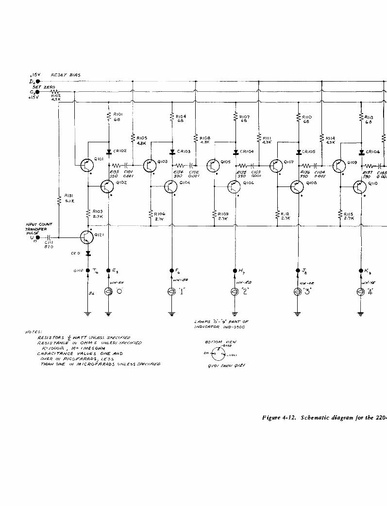
3.2 RING COUNTING UNITS.
Figure 3-2 is a simplified schematic of one of the five ring counting units used in the Type ll50-A Digital Frequency Meter. Each unit consists of a ring-of-ten bistable circuit. Each bistable circuit has one "high -current" transistor capable of driving the associated incandescent lamp for the Numerik indicator for that decade. The first ring counting unit differs from the other four only in the values of its components.
In Figure 3-2,assumethatthecountingunithas been set to its zero state. QlOl will be off and Q102, on. Q102 has its base forward bias current provided by R103 to keep it saturated and passing 80 rna to light the zero lamp in the indicator. This 80-ma current will produce a voltage rise of 5.5volts across R101. The base of Q101 is returned via R102 to the set-zero buss voltage of about -5.0 volts. The base of Ql01 is, therefore, reverse-biased with respect to the emitter and Q101 will remain off. The circuit is stable in this state.
PRINCIPLES OF OPERATION
All other pairs in the ring will have the opposite stable state. The left-hand transistors (Q103, etc), and all saturated right-hand transistors (Q104, etc), areoff. WhenQ103,forexample,ison the R105 clear buss (not the same -5.0 -volt potential as the set-zero buss), it will have nearly 1 rna of forward drive. The drop across the 68-ohm resistor (R104) on the common emitter will be only 0.07 volt and the full 20-volt collector-supply voltage will appear across Rl06. The very small drop in emitter-to-collector voltage of Q 103 will normally be below the conduction knee-voltage of Q104 and will keep it off. Complete cutoff of Ql04 for all possible transistor combinations at elevated temperature is ensured by the silicon diode (CR103 in series with the emitter of D104).
The input signal advances the state of the decade by one stage per pulse. A negative pulse is applied to the base of the advance chain Ql21, turning it off. The on-lamp chain Q102 loses base forward drive and goes off. The common -emitter voltage rises from -5.5 volts to 0 andQlOl goes on. The positive pulse at the common emitter is fed through C101, turning Q103 off and Q104 (the 1 driver) on. Each succeeding pulse applied to Q101 will advance the count by one digit. At the count of 10 the zero pair is switched to the initial conditions, and the negative pulse generated as the 9 lamp extinguishes is fed from this ring counting unit as a carry pulse to the advance driver of the succeeding unit.
In the simplified schematic diagram of Figure 3-2, the zero-set system is depicted as a switch for simplicity. When this switch is opened, the clear buss will return to -20 volts, causing all the left-hand transistors of the bistable circuits to saturate, turning the lamp drives for 1 through 9 off. Q101, on the
EIGHT IDENTICAL UNITS
-~-a--
Figure 3·2. Elementary schematic diagram of a typical ring counting unit.
9
~---T_Y_PE __ ll_SO_-A __ D_IG_I_T_A_L __ F_R_E_O_U_E_NC_Y __ M_E_T_E_R __________________________ ___
other hand, will lose forward bias, desaturate, and permit Q102 to go on, thereby turning on the zero lamp. A fast transistor switch is used in the Type 1150-A to zero set all five ring counting units.
3.3 INPUT AMPLIFIER. The input amplifier in the Type 1150-ADigital
Frequency Meter is a two-transistor feedback amplifier with a voltage gain of 10. The base and the emitter of the input transistor(Q30l, Figure 4-6) are biased to approximately 7 volts by resistors R302 and R303. The total operating current for both transistors is determined by R308 in series with R309. The division of current between the transistors is determined by the ratio of R305 to R306. To obtain a high input resistance, the shield of the input cable and the biasing resistors are bootstrapped by capacitor C302. The input resistance of the amplifier is typically 800 kQ and is determined largely by the collector resistance of Q301.
The amplifier is connected to the input terminals in parallel with the photoelectric -pickoff terminals located at the rear of the instrument when the CHECK switch (S301) is in the position closer to the panel. When the CHECK switch is in the position farther out from the panel, the amplifier is connected to the 100-kc internal crystal oscillator.
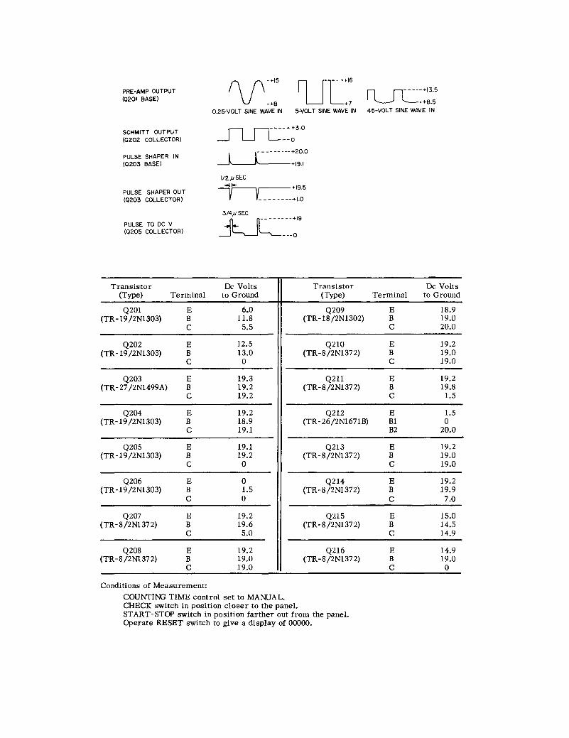
3.4 PROGRAM Cl RCUITS. 3.4.1 SCHMITT CIRCUIT. Transistors Q201 and Q202 (Figure 4-5) are regeneratively connected to form a Schmitt circuit to generate a pulse-type output waveform from the amplified input signal. The output signaL at the collector ofQ202 has a rectangularly shaped waveform of approximately 4-volt amplitude and 0.5-1-lsec rise time.
3.4.2 PULSE SHAPER. Transistor Q203, which is normally biased to saturation, forms a negative pulse with approximately 1-11sec duration. The base of Q203 is capacitively coupled to the output of the Schmitt circuit by capacitors C202 andC203 in parallel. Following negative transitions of the Schmitt circuit, "the coupling capacitors are charged through the relatively low impedance of the saturated pulseshaping transistor. Positive transients of the Schmitt-circuit output waveform cause Q203 to become reverse-biased. The length of cutoff time for Q203 is determined by the discharged time constant of the coupling capacitor and R206. The cut-off time, hence pulse duration, is adjusted with C203. Diode CR201 protects transistor Q203 from excessive reverse bias.
• A. T. r~f~rs to an anchor t~nninal indicat~d on th~ circuit diagram.
10
3.4.3 MAIN GATE. TransistorsQ204and Q205form a series-type gating circuit. The gating signal of approximately 20-volt amplitude (A. T. 203)* is applied to transistor Q204 through biasing resistors. A positive gating signal at A. T. 203 holds Q203 reverse-biased and essentially disconnects the emitter of Q205 so that no signal is amplified by Q205. When the gating signal is approximately at ground, Q204 is biased into conduction and Q205 amplifies and inverts the pulses comingfrom thepulse-shaping transistor Q203. While the main gate is conducting (open), the output signal of transistor Q205 (A.T. 202) consists of positive pulses of approximately 1-11sec duration and 20-volt amplitude. The nonconducting (closed) gate output signal should be 0.25 volt or less.
3.4.4 TIME-BASE GATE. The time-base gating transistorQ206is drivenfrom the collector ofQ211, which is either at 19 volts or at 2 volts above ground. For the 19-volt drive, Q206 has both junctions reverse -biased and acts as an open circuit. For 2-volt drive, the positive pulses from the time-base divider (A. T. 206) saturate Q206 and appear at its collector with very little attenuation.
3.4.5 MAIN GATE FLIP-FLOP. Transistors Q207 and Q208 form a conventional saturating flip-flop circuit. Input pulse steering is provided by CR202, CR303, R218, and R219. A low-impedance source of 0. 6 volt for hold- off bias is provided by silicon rectifier C204. Capacitor C208 couples the pulse output of the display-time generator to the main -gate flipflop and ensures that the main gate is closed during the display interval.
3.4.6 TIME-BASE GATE FLIP-FLOP. Transistors Q210 and Q211 form a conventional saturating flipflop circuit. The positive transition of the gating waveform (A.T. 203) is coupled via capacitor C209 to the base ofQ210which puts Q210 in a nonconducting state and Q211 into a conducting state. The positive transition of the reset pulse is coupled via capacitor C210to the base of transistorQ211 and putsQ211 in a nonconducting state and transistor Q210 into a conducting state.
3.4.7 DISPLAY-TIME GENERATOR. Unijunction transistor Q212 is a delay generator which sets the display time. When Q211 is saturated,capadtor C213 charges through R229 and a display-time control R230. The voltage across C213 (A. T. 208) exponentially approaches +20 volts. At the unijunction firing voltage of approximately 10 volts, a near short ci r.;uit is developed between the emitter and base 1 of Q212 which rapidly discharges C213. The pulse generated across R233 has a fast rise time, 8-volt amplitude, and approximately 70-jlsec total duration.

When the RESET button (S203) is pressed, the display-time generator produces an output pulse by charging C213 through R231. The integrating effect of charging C213 _eliminates multiple pulses due to bouncing of the RESET button.
3.4.8 RESET PULSE GENERA TOR AND AMPLIFIER. Transistors Q213 and Q214 form a saturating monostable multivibrator. Transistor Q214 is normally biased off and Q213 is biased to saturation by R237. A positive pulse coupled from the display-time generator byC216 causes Q213 to turn off. Q214 is regeneratively driven into conduction for a period of time determined by coupling capacitor C215 and resistor R237. A positive pulse of approximately 12-volt amplitude and 17 -msec duration is generated at the collector of Q214.
The monostable circuit normally holds Q216 reverse-biased, withQ215 forward-biased to saturation with a collector-to-emitter drop of only a few tenths of a volt. The output voltage at the reset terminals (A. T. 209 and 210) is, therefore, formed by the voltage divider R241 and R242. This voltage should be 15 ± 1 volts aboveground. When the monostable circuit is not in its normal state, transistor Q215 is reverse-biased, which allows the set-zero line (A. T. 209) to rise to approximately 19 volts, and transistor Q216 is biased on to saturation which forces the reset buss voltage (A.T. 210) to drop to approximately ground.
3.5 TIME BASE.
3.5.1 CRYSTAL OSCILLATOR. Figure 3-3 is an elementary circuit diagram of the 100-kc crystal oscillator in the Type 1150-A Digital Frequency Meter. Transistors Q505 and Q506 provide the gain and the proper terminal impedance for the modifiedPierce crystal oscillator. All of the 60-db, open-loop gain of this transistor pair is used as negative feedback. This results in very stable circuit gain with
+20 VOLTS
Figure 3·3. Simplified circuit diagram of the 100-kc crystal oscillator used in the Type 1150-A Digital Frequency Meter.
PRINCIPLES OF OPERATION
UNIJUNCTION TRANSISTOR
Figure 3-4. Circuit diagram of a relaxation oscillator with a unijunction transistor.
respect to temperature, voltage, and transistor-parameter variations, and hence, excellent oscillatorfrequency stability. The oscillator crystal (X501) is held at constant temperature in a small oven with a hermetically sealed thermostat.
With the TIME BASE switch (S502) set at INT (refer to Figure 4-10), the oscillator output is fed to the buffer amplifier (Q507). For the EXT position of the TIME BASE switch, the buffer amplifier is connected to the EXT 100 KC INPUT connector (1501, at the rear of the instrument) and an externally generated 100-kc signal can be fed into the time base of the Frequency Meter. Diodes CR505 and CR506 protect the buffer amplifier (Q507) against excessive drive and transients. The buffer amplifier (Q507) feeds the 100-kc signal to the time-base divider, to the CHECK switch (S301) for self-check operation, and to the INT 100 kc connector (1502) for calibration or for driving external circuitry.
3.5.2 TIME-BASE DIVIDERS. Fivefrequencydividers provide the standard gate times of 0.1, 1, and 10 seconds in the Type 1150-A Digital Frequency Meter. The dividers use unijunction transistors in synchronized stable relaxation oscillators (see Figure 3-4). The unijunction transistor, or double-base diode, is a silicon unit which will "breakdown" and conduct heavily between emitter and base 1 when the emitter reaches a specified potential (about one-half the supplyvo1tage)with respect to base 1. Before breakdown, the emitter presents a very high resistance to the timing circuit. After breakdown, a high current passes between emitter and base 1, discharging the timing capacitor. When this discharge current reaches a small value, the breakdown condition ends and the timing capacitor begins to recharge toward the supply voltage. The supply voltage to which the upper base is referred is modulated by the input synchronizing pulses. Breakdown is therefore determined by the combination of the rising emitter voltage and the falling synchronizing voltage .1
1Genera[ Electric Transistrx- Manual, 1960, pages 138-145.
11

~---TI_P_E_l_lS_~_A_D_IG_I_T_A_L_F_R_E_Q_U_E_N_CY __ M_E_T_E_R ____________________________ ___
In the Type ll50-A Digital Frequency Meter, the emitter output of each unijunction transistor is a sawtooth waveform of approximately 10-volt amplitude. The waveform at the lower base (test points 401 through 405) is a brief positive pulse. Buffer transistors between the dividers are saturated by this pulse and produce a negative synchronizing pulse for the succeeding stage.
The first divider stage divides the 100-kc oscillator signal by 40 to 2.5 kc; the second stage divides by 25 to 100 cps; the three following circuits each divide by 10 to produce outputs at 10, 1, and 0.1 cps. The high order of division in the first two circuits is possible through careful selection of circuit components and unijunction transistors. Individual temperature compensation is also provided in the first divider. The unijunction transistors in the five dividers are color-coded and should be not interchanged.
3.6 POWER SUPPLIES. A single regulated de source of +20 volts, with
respect to chassis ground, is used for all circuits in the Type 1150-A Digital Frequency Meter. A series-
SECTION4
SERVICE AND
4.1 GENERAL.
We warrant that each new instrument sold by us is free from defects in material and workmanship and that properly used it will perform in full accordance with applicable specifications for a period of two years after original shipment. Any instrument or component that is found within the two-year period not to m~et these standards after examination by our factory, district office, or authorized repair agency personnel will be repaired or, at our option, replaced without charge, except for tubes or batteries that have given normal service.
The two-year warranty stated above attests the quality of materials and workmanship in our products. When difficulties do occur, our service engineers will assist in any way possible. If the difficulty cannot be eliminated by use of the following service instructions,please write or phone our Service Department (see rear cover), giving full information of the trouble
12
type electronic regulator is used for both de voltage control and for ripple reduction. A portion of the output voltage (determined by the voltage divider, R509, R510, and R5ll of Figure 4-10) is compared with a fixed reference voltage (determined by Zener diode CR504) in a differential amplifier (Q503 and Q504). If the output voltage increases, the current in Q504 also increases which decreases the current in Q503. In turn, Q503 reduces the base current in the emitter-follower (Q502) and in the series transistor (Q501), which reduces the output voltage.
Diode CR503 with resistors R504 and R505 supplies the base forward drive for Q503 when power is first applied. As soon as the voltage across CR504 approaches its normal value, CR503 becomes reverse-biased and disconnects the starting circuits.
With the POWER switch in the OFF position, the unregulated power from the +20 -volt supply is disconnected and the cooling fan is off. The power transformer primary winding is, however, still powered, so that the crystal oven is on and crystal temperature is maintained as long as the instrument is plugged into the power line.
MAINTENANCE
and of steps taken to remedy it. Be sure to mention the serial and type numbers of the instrument.
The Type 1150-Afeatures a modular construction that greatly simplifies rep,air. Transistors are on etched boards easily removable from the main structure. To keep "down time" to a minimum, the user can replace a defective board immediately, thus keeping the counter in use while the defective board is being repaired.
Before returning an instrument to General Radio for service,please write to our Service Department or nearest district office (see back cover), requesting a Returned Material Tag. Use of this tag will ensure proper handling and identification. For instruments not covered by the warranty, a purchase order should be forwarded to avoid unnecessary delay.
Components not mounted on etched boards include front-panel controls and switches, indicators, plugs, sockets, power-supply regulating transistor and rectifier diodes, and the power transformer.
4.2 ROUTINE MAINTENANCE.
4.2.1 REPLACING THE INDICATOR LAMPS. Burned-out(open-circuited) lamps will cause a failure in the counting process. To determine the indicator that contains an open lamp, set the CHECK switch to the position further out from the panel and set the COUNTING TIME switch to 1.0 SEC. The ring counting units will operate properly until the open -lamp circuit is energized. That indicator will not display a number and the succeeding indicators will remain at zero. At the end of the counting interval, the faulty indicator will not display a number. To locate which one of the ten bulbs in this indicator is open, either unplug the etched -circuit board for the corresponding ring counting unit and with an ohmmeter check the continuity between the socket pins and the chassis, or apply a low -frequency input signal and observe the counting operation noting the numeral where counting stops.
To gain access to the lamps, turn off the power to avoid shorting the connecting terminals to the chassis, turn the two knurled panel screws on either side of the indicator bank a quarter turn counterclockwise, and pull the indicator bank from the instrument. Eight spare indicator bulbs are provided in the front panel and are accessible when the indicator bank is removed. To remove a burned-out bulb, remove the two screws at the rear of the faulty indicator.
The probability of failure for incandescent bulbs is a function of their operating time. Very few bulbs will have to be replaced until the instrument has accumulated several thousand hours of use, and then the rate of replacement will increase rapidly. We recommend that all bulbs be replaced when this increase is noted (typically after 5000 hours of use). You will notice that used bulbs have darkened due to condensation of filament material on the inside of the glass envelope and may not provide sufficient illumination if continued in use.
The lamps supplied in the Type ll50-A Digital Frequency Meter are General Electric Type 330 or the equivalent. Replacement bulbs should have approximately 0.5 candlepower at 14 volts and 0.08 ampere.
4.2.2 CLEANING THE AIR FILTER. To maintain proper cooling efficiency, the air filter should be cleaned periodically. Local air conditions determine how often this is necessary. To clean, release the air filter from its holder, rap gently to remove excess dirt, flush from the dirty side with hot soapy water, rinse, and let dry. Commercially avialable preparations to increase the filtering efficiency may be applied but are not necessary.
SERVICE AND MAINTENANCE
4.2.3 LUBRICATING THE FAN MOTOR. For long, trouble -free operation, lubricate the fan motor at least once a year with SAE 20 or 30 premium -quality oil. There are two lubricating holes, one in each of thebrass brackets on either side ofthemotorlaminations.
4.2.4 CHECKING THE 100-KC CRYSTAL-OSCILLATOR FREQUENCY. The accuracy of the frequency measurements made with the Type 1150-A depends on the frequency accuracy of the crystal oscillator. This oscillator is very stable and should rarely require resetting. To check the oscillator frequency, observe the signal at the INT 100 KC connector at the rear of the instrument with a General Radio Type 1130-A Digital Time and Frequency Meter, or use a beat method with a stable 100-kc standard frequency signal. For the comparison method, use a signal whose frequency is known to at least one part in 105 and preferably 1/2 part in 106.
Although the power-line frequency can be measured to considerable accuracy (±0.017% for a 100-second average taken by manual multiple-period gating: refer to paragraph 2.2.2), it should not be used to set the accuracy of the Frequency Meter, since the power-line frequency varies in the course of a day (typically ±0.1%).
To adjust the 100-kc oscillator frequency, turn the variable air capacitor located near the INT 100 KC plug (accessible when the instrument cabinet is removed~ refer to paragraph 2.2.2).
4.3 INTERNAL ADJUSTMENTS.
4.3.1 GENERAL. Normally, most of the factory-set adjustments will not require any attention. Those adjustments that may occasionally be necessary (as, for instance, after replacement of a transistor) are described in the following paragraphs. Before making these adjustments, be sure that the TIME BASE switch is set to INTand thatthepower-supply and input-signal characteristics are correct (refer to paragraphs 2.2.4 and 2.2. 7).
4.3.2 POWER-SUPPLY ADJUSTMENT. The trimmer potentiometer, R510, located on the power -supply board, adjusts the regulated 20-volt de supply. The voltage between anchor terminal 507 and ground should be set to within 5% of 20 volts.
4.3.3 ADJUSTMENT OF 11-:IE DURATION OF THE FIRST-COUNTING-UNIT INPUT PULSE. Apply a 220-kc signal to the INPUT terminals. Adjust the duration of the input pulse with the small ceramic trimmer
13

~--~TY~P~E~l~lS~O-~A~D~I~G~I~T~A=L~F~R~E~Q~U~E~N~C~Y-=M=E~T=E=R----------------------------
capacitor, C203, located on the horizontally mounted program board. Set C203 to the middle of the range for which the instrument properly indicates 220 kc. This adjustment is not critical.
4.3.4 ALIGNMENT OF THE TIME-BASE DIVIDER BOARD. The time-base divider board (Type 1150-4040) consists of five RC oscillators, which are locked to each other in chain fashion and which divide the 100-kc crystal-oscillator signal for the 10-,1-, and 0.1-cps outputs. The oscillators are carefully aligned at the factory and should not be adjusted unless there is a positive indication of error in division ratio. An error in oscillator alignment will be indicated by an incorrect reading when the Type 1150-A is operated with the CHECK switch in the position further out from the panel. The adjusting potentiometer and unijunction transistor associated with each_oscillator arelistedin Table 4-1 and identified in Figure 4-1. In Figure 4-1 the transistors have been removed from their sockets.
The unijunction transistors installed at the factory have been selected for proper temperature coefficient and have been color-coded with their corresponding sockets. Be sure that the unijunction transistors supplied are not interchanged in the oscillators. An unselected unijunction transistor should operate satisfactorily for the range of temperatures encountered in most installations.
An error in the dividers can be observed with an oscilloscope or frequency meter by comparing the input and output pulse repetition rates.
To adjust the oscillators, adjust the trimming potentiometers to their free-running frequencies (refer to Table 4-1) with an instrument such as the General Radio Type 1130-A Digital Time and Frequency Meter. The oscillator is made free-running when the unijunction transistor of the next higher divider is unplugged. The 2.5-kc oscillator is made free-running when the TIME BASE switch is set to EXT.
4.4 TROUBLE-SHOOTING PROCEDURE. The simplest method oi locating a malfunction
within the instrument is to observe the indicator readings and the COUNTING lamp while operating the panel controls. Section 3, Principles of Operation, and Figure 3-1, the block diagram, will help determine which circuits are used for the various positions of the panel controls. The schematic diagrams, parts lists, part-locating drawings, voltage tables, and waveforms are given at the end of this section.
CAUTION
When trouble-shooting, be careful to avoid short-circuits, between components and chassis, connectors, etc. In some cases, even a momentary shortcircuit can destroy a transistor.
Table 4-2 (page 16) lists possible failures and their probable causes.
TABLE 4-1
Locked Unlocked Unijunction Division Adjustment Output (Free-Running) Transistor Ratio Potentiometer Frequency Period
Q401 40:1 R401 2.5 kc 405 j.lSeC
Q403 25:1 R408 100 cps 10.2 msec
Q405 10:1 R414 10 cps 105 msec
Q407 10:1 R427 1 cps 1.05 sec
Q409 10:1 R428 0.1 cps 10.5 sec
14
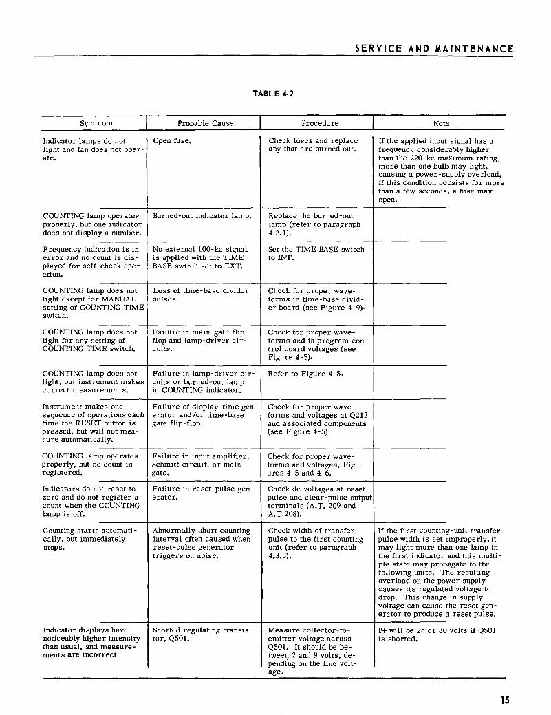
Symptom
s do not Indicator lamp light and fan do es not oper-ate.
COUNTING lam properly, but o does not displa
p operates ne indicator y a number.
cation is in Frequency indi error and no co played for self
unt is dis-check oper-
ation.
p does not COUNTING lam light except for setting of COUNT
MANUAL lNG TIME
switch.
p does not COUNTING lam light for any se COUNTING TIM
tting of E switch.
p does not COUNTING lam light, but instrum correct measur
ent makes ements.
es one Instrument mak sequence of ope time the RESET pressed, but wi sure automatica
rations each button is
11 not mea-lly.
p operates COUNTING lam properly, but no registered.
count is
ot reset to Indicators do n zero and do not count when the lamp is off.
register a COUNTING
automati-Counting starts cally, but immed iately stops.
ys have er intensity
Indicator displa noticeably high than usual, and ments are inco
measure-rrect
SERVICE AND MAINTENANCE
TABLE 4-2
Probable Cause Procedure
Open fuse. Check fuses and replace any that are burned out.
Burned-out indicator lamp. Replace the burned-out lamp (refer to paragraph 4.2.1).
No external 100-kc signal Set the TIME BASE switch is applied with the TIME to INT. BASE switch set to EXT.
Loss of time-base divider Check for proper wave-pulses. forms in time-base divid-
er board (see Figure 4-9)·
Failure in main-gate flip- Check for proper wave-flop and lamp-driver cir- forms and in program con-cuits. trol board voltages (see
Figure 4-5).
Failure in lamp-driver cir- Refer to Figure 4-5. cuits or burned-out lamp in COUNTING indicator.
Failure of display-time gen- Check for proper wave-erator and/or time-base forms and voltages at Q212 gate flip-flop. and associated components
(see Figure 4-5).
Failure in input amplifier, Check for proper wave-Schmitt circuit, or main forms and voltages, Fig-gate. ures 4-5 and 4-6.
Failure in reset-pulse gen- Check de voltages at reset-erator. pulse and clear-pulse output
terminals (A.T. 209 and A.T.208).
Abnormally short counting Check width of transfer interval often caused when pulse to the first counting reset-pulse generator unit (refer to paragraph triggers on noise. 4.3.3).
Shorted regulating transis- Measure collector-to-tor, Q501. emitter voltage across
Q501. It should be be-tween 2 and 9 volts, de-pending on the line volt-age.
Note
If the applied input signal has a ably higher
aximum rating, frequency consider than the 220-kc m more than one bulb may light,
upply overload. rsists for more , a fuse may
causing a power-s If this condition pe than a few seconds open.
If the first countin pulse width is set i
g-unit transfermproperly, it none lamp in and this multiagate to the
may light more tha the first indicator ple state may prop following units. The resulting overload on the po wer supply causes its regulate d voltage to drop. This change in supply voltage can cause t he reset gen
a reset pulse. erator to produce
Bt- will be 25 or 30 volts if Q501 is shorted.
15

16

PARTS LISTS AND SCHEMATICS
On the following pages appear parts lists, schematic diagrams, voltage tables, waveforms and etched-board layouts, which should prove helpful in trouble-shooting. These data are
a"anged by circuit as follows:
Circuit
Type 1150-A Block Diagram and Interior View Type 1150-4020 Program Control Circuit • Type 1150-4030 Input Amplifier Circuit Type 1150-4040 Time-Base Divider Circuit Type 1150-4050 Power Supply and Oscillator Circuits Type 1150-D1 220-kc Ring Counting Unit Type 1150-D2 30-kc Ring Counting Unit Type 1150-A Interconnection Diagram • •
NOTES FOR PARTS LISTS
Type designations for resistors and capacitors are as follows:
COA · Capacitor, air COC • Capacitor, ceramic COE • Capacitor, electrolytic COM • Capacitor, mica COP • Capacitor, plastic COT • Capacitor, trimmer
POSW • Potentiometer, wire-wound REC • Resistor, composition REF • Resistor, film REPR ·Resistor, precision REW • Resistor, wire-wound
Resistors J1 watt unless otherwise specified.
Pages
19 20, 21 23 25 26, 27
• 28, 29
30, 31
32
All resistances are in ohms, unless otherwise indicated by k (kilohms) or M (megohms).
All capacitances are in picofarads, unless otherwise indicated by pf (microfarads).
17

18
R401 Q401
TP401
R408 Q403
R414 Q405 TP40
R427--~~...i.l
Q407 TP404
R428 ------1 Q409 --·-.. =-· TP405------~~~~~~~
2.5-kc OSCILLATOR
100-cps OSCILLATOR
10-cps OSCILLATOR
1.0 -cps OSCILLATOR
0.1-cps OSCILLATOR
Figure 4-1. Time-base divider etched board used in the Digital Frequency Meter.

T501
TYPE 1150-4050 POWER SUPPLY AND OSCILLATOR
!.. " --v.---· ..;;__JJ
TYPE 1150-D2 RING COUNTING UNITS
· TYPE 1150-DI RING COUNTING UNIT
TYPE 1150-4040 TIME BASE DIVIDER
TYPE 1150-4030 INPUT A.MPLIFIER
I , TYPE
1150-4020 PROGRAM CONTROL

TYPE 1150-A BLOCK DIAGRAM AND INTERIOR VIEW
INPUT AMPLIFIER
ETCHED BOARD 300 SERIES COMPONENTS
-----Q CHECK
PROGRAM BOARD,
GATING SIGNAL
I I I I
5 NUMERIK INDICATORS TYPE IND-300
RESET BUSSES
L ____________ _ -~
I I I I I I
MAIN GATE
FLIP-FLOP 0207, 020B
COMPLIMENTARY INPUT
TIME BASE
SE r T:_t__ _ _t_.:.:_RESET
GATE f-----4---l TIME BASE
GATE FLIP-FLOP 0210,0211 0206 GATING
~~----'SIGNAL
RESET PULSE GENERATOR
AND AMPLIFIER 0213, 0214, 0215, 0216
DISPLAY TIME
GENERATOR 0212
~--~RESET I
100 kc ~00 SERIES COMPONENTS --------
____________ __J __ _j
r------ -, 1 1oo-kc I I POWER CRYSTAL I TIME BASE 0.1 SEC I SUPPLY AND OSCILLATOR 100 kc DIVIDER I REGULATON AND ETCHED BOARDI-;--.:..
1 .:::SE:::.:C::...._o
I 0501, 0502, AMPLIFIER 400 SERIES 10 SEC 0503, 0504, 0505, 0506 COMPONENTS
I 0507 I I POWER SUPPLY 8 OSCILLATOR BOARd L _ 500 SERIES COMPONENTS_ J
MANUAL o
_ _ ~COUNTING ~TIME
Figure 4-2. Block diagram of the Type 1150-A Digital Frequency Meter.
I I
~ DISPLAY
TIME

20
TIME BASE (A.T. 206)
MAIN GATE TRIGGERS (0206 COLLECTOR)
MAIN GATE (0207 COLLECTOR)
TIME BASE GATE FLIP-FLOP (0211 COLLECTOR)
DISPLAY TIME GENERAWR (0212 EMITTER)
RESET TRIGGER (0212 BASE ONE)
RESET GENERATOR (0213 BASE)
RESET GENERATOR OUT (0214 COLLECTOR)
SET ZERO OUT (0215 EMITTER)
RESET PULSE OUT (0216 EMITTER)
COUNTING TIME
0.1, I, OR 10 SEC
DISPLAY TIME
0.5 TO 5 SEC
RESET TIME 3m SEC
+(0 TO 10) SEC
+4--~ L 0-- ~ -----A------~------~-------J~-----J~------
15 TO 20J.I SEC
+4--]\__
0;~ T~ SEC____j ___ -''-----------------'~'----L +2--.1\., o-- ~
5p SEC •l::lJ 1,__----..J ~
COUNTING TIME
+19=rl_
+ 1.5 f4-o.l ------------...J DISPLAY TIME PLUS 3m SEC
+10=:/1_ +1.5 ~ ---------.J'
DISPLAY TIME 0.5 TO 5 SEC
+8---" +0.5 ____ ,_~
o----le--+4 --------------------' ;::::j 14m SEC
+30~
+19 14-o-1 --------------' 3m SEC
+19JL +7 ~ -------------~
3m SEC
·':;~=a----------------' 3m SEC
·~~::l_j ~
3m SEC
PRE-AMP OUTPUT (0201 BASEl
SCHMITT OUTPUT (0202 COLLECTOR)
PULSE SHAPER IN (0203 BASE)
PULSE SHAPER OUT (0203 COLLECTOR)
PULSE TO DC V (0205 COLLECTOR)
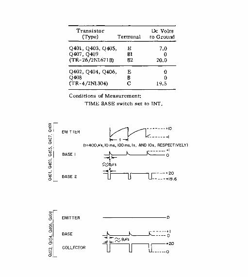
Transistor (Type) Terminal
Q201 E (TR -19/2N1303) B
c
Q202 E (TR -19/2N1303) B
c
Q203 E (TR-27/2N1499A) B
c
Q204 E
(\ (\-+15
v -+8
n n---+16 . U L .. 7
0.25-VOLT SINE WAVE IN 5-VOL T SINE WAVE IN
II 11-----+3.0
_j LJ L_ __ o
~::~;0 l/2pSEC
... to- +19.5
~•1.0 3/4pSEC ..Jl.. n--------+19
_j~~---0
De Volts to Ground
6.0
Transistor (Type)
Q209 11.8 (TR -18/2N1302)
5.5
12.5 Q210 13.0 (TR-8/2N1372)
0
19.3 Q211 19.2 (TR-8/2N1372) 19.2
19.2 Q212
n n·----+13.5
I l.__) l...__-+8.5
45-VOL T SINE WAVE IN
De Volts Terminal to Ground
E 18.9 B 19.0 c 20.0
E 19.2 B 19.0 c 19.0
E 19.2 B 19.8 c 1.5
E 1.5 (TR -19/2N1303) B 18.9 (TR-26/2N1671B) B1 0
c 19.1 B2 20.0
Q205 E 19.1 Q213 E 19.2 (TR-19/2N1303) B 19.2 (TR-8/2N1372) B 19.0
c 0 c 19.0
Q206 E 0 Q214 E 19.2 (TR -19/2N1303) B 1.5 (TR-8/2NI372) B 19.9
c 0 c 7.0
Q207 E 19.2 Q215 E 15.0 (TR-8/2N1372) B 19.6 (TR-8/2N1372) B 14.5
c 5.0 c 14.9
Q208 E 19.2 Q216 E 14.9 (TR-8/2N1372) B 19.0 (TR-8/2N1372) B 19.0
c 19.0 c 0
Conditions of Measurement:
COUNTING TIME control set to MANUAL. CHECK switch in position closer to the panel. START-STOP switch in position farther out from the panel. Operate RESET switch to give a display of 00000.

0 0
L . Figure 4-·5. Program control etched board.
RESISTORS CAPACITORS
R201 2.4 k ±5% 1/2 w REC· 20BF(242B) C201 0.0022 fJf ±10% 500 dcwv COC-62(222C) R202 2.2 k ±5% 1/2 w REC- 20BF(222B) C202 68 pf ±5% 500 dcwv COM-22D(680B) R203 820 n ±5% 1/2 w REC-20BF(821B) C203 8-50 pf COT-29-4 R204 2.4 k ±5% 1/2 w REC-20BF(242B) C204 820 pf ±10% 500 dcwv COC-62(821C) R205 820 n ±5% 1/2 w REC-20BF(821B) C205 820 pf ±10% 500 dcwv COC-62(821C) R206 51 k ±5% 1/2 w REC-20BF(513B) C206 0.0033 fll ±10% 500 dcwv COC-62(332C) R207 5.1 k ±5% 1/2 w REC-20BF(512B) C207 0.0033 fll ±10% 500 dcwv COC-62(332C) R208 3.9 k ±5% 1/2 w REC- 20BF(392B) C208 470 pf ±10% 500 dcwv COC-62(471C) R209 4.7 k ±5% 1/2 w REC-20BF(472B) C209 820 pf ±10% 500 dcwv COC-62(821C) R210 510 n ±5% 1/2 w REC- 20BF(Sll B) C210 820 pf ±10% 500 dcwv COC-62(821C) R211 1 k ±5% 1/2 w REC- 20BF(1 02B) C211 820 pf ±10% 500 dcwv COC-62(821C) R212 4.7 k ±5% 1/2 w REC- 20BF(472B) C212 820 pf ±10% 500 dcwv COC-62(821C) R213 1 k ±5% 1/2 w REC- 20BF(l02B) C213 60 1-'f +100-10% 25 dcwv COE-47 R214 2.2 k ±5% 1/2 w REC- 20BF(222B) C214 820 pf ±10% 500 dcwv COC-62(821C) R215 2.2 k ±5% 1/2 w REC- 20BF(222B) C215 0.22 1-'f ±20% 25 dcwv COC-4(2240) R216 13 k ±5% 1/2 w REC-20BF(l33B) C216 0.0033 fJf ±10% 500 dcwv COC-62(332C) R217 13 k ±5% 1/2 w REC-20BF(133B) C217 0.1 iJf ±20% 25 dcwv COC-4(1040) R218 1 k ±5% 1/2 w REC- 20BF(102B) C218 470 pf ±10% 500 dcwv COC-62(471C) R219 1 k ±5% 1/2 w REC- 20BF(102B) R220 l.Sk ±5% 1/2 w REC- 20BF(152B) R221 2.2 k ±5% 1/2 w REC- 20BF(2 22B) R222 200 n ±5% 1/2 w REC- 20BF(201B) DIODES R223 4.3 k ±5% 1/2 w REC- 20BF( 432B) R224 4.3 k ±5% 1/2 w REC- 20BF( 432B) CR201 2RED1016/1N645 R225 24 k ±5% 1/2 w REC- 20BF(243B) CR202, CR203 2RED1006/1Nll8A R226 24 k ±5% 1/2 w REC- 20BF(243B) CR204 2RED1016/1N645 R227 l.Sk ±5% 1/2 w REC-20BF(152B) CR205 2REZ1006/1N753A R228 2.7 k ±5% 1/2 w REC- 20BF(27 2B)
TRANSISTORS R229 6.8k ±5% 1/2 w REC- 20BF( 682B) R230 100 k ±20% 1150-0400 Q201 TR-19/2N1303 Q209 TR-18/2N1302 R231 2.7 k ±5% 1/2 w REC- 20BF(272B) Q202 TR-19/2N1303 Q210 TR-8/2N1372 R232 510 n ±5% 1/2 w REC-20BF(511B) Q203 TR-27/2N1499A Q211 TR-8/2N1372 R233 47 n ±5% 1/2 w REC-20BF(470B) Q204 TR-19/2N1303 Q212 TR-26/2N1671B R234 4.3 k ±5% 1/2 w REC- 20BF( 432B) Q205 TR-19/2N1303 Q213 TR-8/2N1372 R235 24 k ±5% 1/2 w REC- 20BF(243B) Q206 TR-19/2N1303 Q214 TR-8/2N1372 R236 l.Sk ±5% 1/2 w REC-20BF(152B) Q207 TR-8/2N1372 Q215 TR-8/2N1372 R237 24 k ±5% 1/2 w REC-20BF(243B) Q208 TR-8/2N1372 Q216 TR-8/2N1372 R238 2.2 k ±5% 1/2 w REC-20BF(222B) R239 2.4 k ±5% 1/2 w REC- 20BF(242B) MISCELLANEOUS R240 2.7 k ±5% 1/2 w REC-20BF(272B) R241 75 n ±5% 1/2 w REC- 20BF(7 SOB) P201 Pilot Light 2LAP-10 R242 150 n ±5% 2w REW- 3C(151B) S201 Switch SWRW-3120 R243 300 n ±5% 1/2 w REC-20BF(301B) S202 Switch SWP-22 R244 1 k ±5% 1/2 w REC-20BF(102B) S203 Switch SWP-.23

COUNTING TIME SEC
~0 10
Q.J MANUAL
lfNP(IT' .Sitf'-'"'<) (fA!'oM r;311 e /
5201
ro SO$t111 ~8 -~--~--+-+
C2.0I o.oozz.
1R2o3
82.0
INt<>t./7' $C¥MI1"T
1(2/9 0.1
i'!Mt::BASE' l)!VI'J)E:R PU~SE: (POSITIVE.)
l~S£4>---~.v~¥!:!._-~v~r_-~e~e~---,
1.0 SEC. '>----~W.~'H'=-!'..Vr!.:-~B~<tt::.___...,
o.r SE
A.T.203
Rzoz 2.'2K
~--~~-='---"=-- A.7:20!1(.!1-<~D SET') ,_ _ _!J~==~- II.T. eos(l>tSI't,., Y .:::!E~AY}
0-.j..!!IV!:!.H:!-~'-C~~!.;C-!::BI!,___J .i'O!J, 1 (r.i'O >")
=-he~K,.-----J&>?J, ~JVP RN""E)
CMRV SOI0-5;$1$"
L-!:!:.!2:..:£.==---- 5ZOI,I04R R£,.,4rl .srNAi!r-.srot<>
RZI5 Z.ZK
Mt'111Vt:$"Hr#' F.t.IP-I"J.4P
O=KNOI!J C<:YVTROL
~ = SCREWD.e/Y£~ CONT,e()L
R227 1.5K
C2/J 820
TIM# 8,1JSI'
(i"'TI ,-J.IP -;rt.iiP
C214 820
R2Z8 i!.ZK
Figure 4-4. Schematic diagram of tb

9212 (j)201 T#£L/ f1,Z//
9215 Tf.IRL/(jJ.Z/<1
TYPE 1150-4020 PROGRAM CONTROL CIRCUIT
WH-GN-.8£
--------------------------------------------------------------------------------------------------l~_! __ _._t20V
f/T202. ------------------------------------~-~~ ~ PULSE ~ TO Fltf!ST L)ECAlJE
NH-.eD-BK--:J
)
)2//
L
R229 !;.8K
,---5204
fi.T.W7 kcw
1 £Z3b0 0001 /00/t
the program control circuit.
TO SOI0/1 u17
Q 2.12.
RZ34 4.31<.
C217 0.1
9215
A.T.Z09
CR2.o.f
HIII·BR·SK. TO S41#Ji Cs
Sir z.-~c PV4-S6' aur
'15V
t-----~--~A~·~·Z~/~0~--~~~~--I'IH-~·Bi. TO s~_,
+ (220
~,A(F
RISer ;~~v .. 66 OIJ7"
21

~ 1150-0730/ 1
R305
R302
.. 01
111111111 J Ill Figure 4-7. Input amplifier etched board.
RESISTORS
R301 100 k ±5% 1/2 w REC-20BF(104B) R302 13 k ±5% 1/2 w REC-20BF(133B) R303 7.5 k ±5% 1/2 w REC-20BF(752B) R304 6.2 k ±5% 1/2 w REC-20BF(622B) R305 43 k ±5% 1/2 w REC-20BF(433B) R306 4.3 k ±5% 1 /2 w REC- 20BF( 432B) R307 4.7 k ±5% 1/2 w REC-20BF(472B) R308 470 n ±5% 1/2 w REC - 20BF(471B) R309 5.1 k ±5% 1/2 w REC-20BF(512B)
CAPACITORS
C301 0.1 fjf +80-20% 50 dcwv COC-63-3 C302 200 fJf 6 dcwv COE-44 C303 40 fjf 6 dcwv COE-54 C304 40 fjf 6 dcwv COE-54
TRANSISTORS
Q301 TR- 21/2N338 II Q302 TR-23/2N520A
MISCELLANEOUS
J301 Jack BP-10, 1 J302 Jack BP-10, 13/32 J303 Jack CDSJ-20 S301 Switch SWP-22 S0301 Socket CDMS-38, 18
GR EE N P/1/NT EIX'E .FO.e ! OENT/.FIC'IlTIO/V
Transistor De Volts (Type) Tenninal to Ground
Q3m E &7 (TR-21/2N338) B 6.9
c 15.4
Q302 E 15.5 (TR-23/2N520A) B 15.4
c 11.8
Conditions of Measurement:
No input signal.

BOTTOM VIEW 8115£ EMBCOU Q30/ Q$02
C.OI F o.1 i~
INPILr
fl303
7.SK
TYPE 1150-4030 INPUT AMPLIFIER CIRCUIT
v --~------------~~~
OUTPUT i.J£-(noz)
• • • • • •
17~-e_f:!DII' 18 l)l/rte/T I
1¥11-RIJ "611 t-ffz.,)
I I ____ _
Figure 4-6. Schematic diagram of the input amplifier.
OPTICI'IJ.. PI~K tiP (~OCI'ITif" Zl ON I'IEI'IR 0~ I""'T.)
.J 303 (+2o>')
Ea w.v-~191'
_x~qf-:-1 -A!"""DI I
<l'iV4f-t'~ruY,ll I I
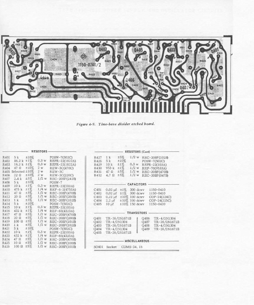
Figure 4·9. Time-base divider etched board.
RESISTORS RESISTORS (Cont)
R401 5k ±10% POSW ·7(502C) R427 1 k ±5% 1/2 w REC-20BF(102B) R402 18.2 k ±1% 0.3 w REPR·22(1822A) R428 5k ±10% POSW -7(502C) R403 18.2 k ±1% 0.3 w REPR -22(1822A) R429 10 k ±1% 0.3 w REPR -22(103A) R404 47 n ±10% 2w REW -3C(470C) R430 953 k ±1% 1/2 w REF -70(9533A) R405 Selected ± 10% 2w REW-3C R431 47 n ±5% 1/2 w REC-20BF(470B) R406 22 n ±10% 2w REW -3C(220C) R432 4.7 n ±5% 1/2 w REC- 20BF(047B) R407 2.4 k ±5% 1/2 w REC-20BF(242B) R408 5k ±10% POSW-7
CAPACITORS R409 10 k ±1% 0.3 w REPR -22(103A) R410 475 k ±1% 1/4 w REF-6-2(4753A) C401 0.02 fll ±1% 300 dcwv 1150-0410 R411 47 n ±5% 1/2 w REC- 20BF( 470B) C402 0.02 1-lf ±1% 300 dcwv 1150-0410 R412 20 n ±5% 1/2 w REC- 20BF(200B) C403 0.22 1-lf ±10% 100 dcwv COP-24(2 24C) R413 1 k ±5% 1/2 w REC-20BF(102B) C404 2.2 1-lf ±10% 100 dcwv COP-24(225C) R414 5k ±10% POSW-7(502C) C405 10 !Jf ±10% 150 dcwv ll50-0420 R415 10 k ±1% 0.3 w REPR-22(103A) R416 432 k ±1% 1/4 w REF-65(4323A)
TRANSISTORS R417 47 n ±5% 1/2 w REC-20BF(470B) R418 20 n ±5% 1/2 w REC-20BF(200B) Q40l TR-26/2Nl671B Q406 TR-4/2N1304 R419 100 n ±5% 1/2 w REC-20BF(101B) Q402 TR -4/2N1304 Q407 TR-26/2Nl671B R420 i k ±5% 1/2 w REC-20BF(102B) Q403 TR-26/2N1671B Q408 TR -4/2N1304 R421 5k ±10% POSW-7(502C) Q404 TR-4/2N1304 Q409 TR-26/2N1671B R422 10 k ±1% 0.3 w REPR -22(103A) Q405 TR-26/2N1671B R423 432 k ±1% 1/4 w REF-65(4323A) R424 47 n ±5% 1/2 w REC-20BF(470B) MISCELLANEOUS R425 10 n ±5% 1/2 w REC-20BF(100B) R426 100 n ±5% 1/2 w REC-20BF(101B) S0401 Socket CDMS-34, 18
"'~ 0
"' a .-.: 0
"' a
"' 0
"' a o-i 0
"' a
0
"' a
00 0
"' a -<5 0
"' a ..,-0
"' a
"' 0
"' a
Transistor De Volts (Type) Terminal to Ground
Q401' Q403, Q405, E 7.0 Q407, Q409 Bl 0 (TR-26/2Nl671B) B2 20.0
Q402, Q404, Q406, E 0 Q408 B 0 (TR-4/2Nl304) c 19.5
Conditions of Measurement:
EMITTER
BASE I
BASE 2
EMITTER
BASE
TIME BASE switch set to INT.
vv--c:------+10
I--t~ -------+1
(t=400Jis, 10 ms, lOOms, Is, AND lOs, RESPECTIVELY)
~·I __,~.- 0
~8}/s
-"1.1"- ---+20
"LJlJLL ---+19.6
----------0 ' ' .------+1 ~'-----0 ---< 1- rv 8Jis ~ lo- rv +20
COLLECTOR ~0

AI 3@
+20V R401 SK z.
R40Z H\.'Z.I( 0.3W
'l.$/t:G
R403 18.~K
0.311/
/OOKc FROM /1, T. 512
82.
TP-1()/
C401 R4or..
22 o.ot.
R4o& 5K
R"\05 SELE:CTe7>
R4o'> 440$ ~401 JAIK
Q""02 TP-H2
R40 R412 C41;)1!
/OK
O.!JW 0,02. 2.0
TYPE 1150-4040 TIME-BASE DIVIDER CIRCUIT
R41~ IOC R41? R4Z.l 0.1~ R43/
5t<. I~ 5K
4'7
Q405 C/407 Q40~
Q404 TP-hlfJ t~ TP405
A.415 C"'o3 R-418 R42Z
C404 ~4Z5 R42' R432 C4~
101< 2.0 !OK 10 /OK 4.? o.zz o.3w' 2.2..,1" IO...F
0.3H o.aw
D~.~--------------~--------~--------~-----------+--~~----~~--~~----------~~-i------~----~--~-------+--~4-----~~----~-J~------J-~--~----~----_J GltiD 4o ro I.OtnoGe _______ _...,,_ _____ .es ra; DIYIDIII!. ______ t-----'":'o'"''o•lf!. ______ ...,_. _____ 1o:1 o1n.t>~rR -------+----·'o: 1 otvtPIA! I
2.5"Kt: ()tiTPUr ltJOC O()TPVT I(JC OUTPur IC Ot.ITPt.IT o.;c OVTPqr --t
BOTTOM /1/EW
··~·· £NI EM6tl/SE . COLL
8/ISE 1
.)ASi 1 J'IISE 2
0401, 0403, 0405, 0407, 0409
•
.s-o -901
..SOCK# r CtJNIVICTI"NS ~~ 18
• •
' • •
~ ':i
. { . . .. •
~ ~ " .. ' ' ,, ~
.........
" \) "' ~ ,.,
1.. ~ ;) ~ 0 0 l,j
~ ~ ..... Iii ..,
'
Figure 4-8. Schematic diagram of the time-base divider.
J8 Of.,- v,s OVTPVT Ol.ITPVT OtiTPUT
0.1 .SEC PULSES I SEC PVLSES 10 SEC PULSES
TO S20/1 10/F TO S20f; 103F TO s201, 10.5 F
25
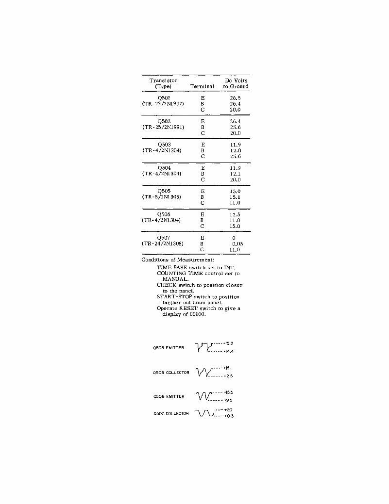
Transistor De Volts (Type) Terminal to Ground
Q501 E 26.5 (TR-22/2N1907) B 26.4
c 20.0
Q502 E 26.4 (TR-25/2N1991) B 25.6
c 20.0
Q503 E 11.9 (TR-4/2N1304) B 12.0
c 25.6
Q504 E 11.9 (TR-4/2N1304) B 12.1
c 20.0
Q505 E 15.0 (TR-5/2N1305) B 15.1
c 11.0
Q506 E 12.5 (TR-4/2N1304) B 11.0
c 15.0
Q507 E 0 (TR-24/2N1308) B 0.05
c 11.0
Conditions of Measurement:
TIME BASE switch set to INT. COUNTING TIME control set to
MANUAL. CHECK switch to position closer
to the panel. START-STOP switch to position
farther out from panel. Operate RESET switch to give a
display of 00000.
0505 EMITTER
0505 COLLECTOR
0506 EMITTER
0507 COLLECTOR
I )I_;---- +15.3 y [_ ____ +14.4
----+15.1
V\r!'_ ____ +2.5
V\f'_---- +15.5
------+9.5
'\ f\ . --- +20 v v-----+0.3

0
L Figure 4-11. Power supply and oscillator etched board.
RESISTORS CAPACITORS (Cont}
R501 0.47 n ±10% 2w REW -3C(0047C) C507 27 pf ±5% 500 dcwv COM-220(270B) R502 200 n ±5% 1/2 w REC-20BF(201B) C508 0.001 f}f ±2% 500 dcwv COM-5E(102A1) R503 1 k ±5% 1/2 w REC-20BF(102B) C509 0.1 fJ{ +80-20% 50 dcwv COC-63-3(1040) R504 4.7 k ±5% 1/2 w REC- 20BF(472B) C510 0.1 fJ{ +80- 20% 50 dcwv COC-63-3(1040) R505 2.2 k ±5% 1/2 w REC- 20BF(222B) C511 0.01 fJ{ ±20% 500 dcwv COC-62(1030) R506 1.2k ±5% . 1/2 w REC- 20BF(122B) C512 0.01 f}f ±20% 500 dcwv COC-62(1030) R507 1 k ±5% 1/2 w REC-20BF(102B) C513 1 f}f ±20% 25 dcwv COC-4(1050) R508 3.9 k ±5% 1/2 w REC-20BF(392B) C514 0.1 fJ{ +80-20% 50 dcwv COC-63-3(1040) R509 1 k ±1% 0.3 w REPR-22(102A) R510 2k ±10% POSW-7(202C) DIODES R511 1.5k ±1% 0.3 w REPR-22(152A)
CR501, CR502 2RE1005/1N3660 R512 2.7 k ±5% 1/2 w REC- 20BF(272B) R513 3.3 k ±5% 1/2 w REC-20BF(332B) CR503 2RED1016/1N645
R514 7.5 k ±5% 1/2 w REC-20BF(752B) CR504 2REZ1013/1N941
R515 24 k ±5% 1/2 w REC- 20BF(243B) CR505, CR506 2RED1006/1Nll8A
R516 2.2 k ±5% 1/2 w REC- 20BF(222B) TRANSISTORS R517 3.3 k ±5% 1/2 w REC-20BF(332B) R518 24 k ±5% 1/2 w REC- 20BF(243B) Q501 TR-22/2N1907 Q505 TR -5/2N1305 R519 1 k ±5% 1/2 w REC- 20BF(102B) Q502 TR-25/2N1991 Q506 TR-4/2N1304 R520 330 k ±5% 1/2 w REC- 20BF(334B) Q503 TR-4/2N1304 Q507 TR-24/2N1308 R521 1 k ±5% 1/2 w REC-20BF(l02B) Q504 TR - 4/2N1304 R522 1 k ±5% 1/2 w REC- 20BF(102B) R523 2.2 k ±5% 1/2 w REC-20BF(222B) FUSES R525 100 k ±5% 1/2 w REC-20BF(l04B) R526 470 ±5% 1/2 w REC-20BF(471B) ll5v:
11230 v: R527 lOOk ±5% 1/2 w REC-20BF(104B) F501 0.6 a FUF-1 F501 0.3 a FUF-1 F502 0.6 a FUF-1 F502 0.3 a FUF-1
CAPACITORS.
C501 3000 f}f +100-10% 30 dcwv 1150-0440 MISCELLANEOUS
C502 0.01 f}f ±20% 500 dcwv COC-62(1030) J501 Jack COSJ-24 S501 Switch SWT-333 C503 p.Ol fJ{ ±20% 500 dcwv COC-62(1030) J502 Jack COSJ-24 S502 Switch SWT- 16 C504 6.8 fJf ±20% 35 dcwv COE-61(6850) M501 Motor M00-23 T501 Transformer 0485-4013 C505 487 pf ±2% 500 dcwv COM-5E(4870Al) PL501 Plug COPP-10 X501 Crystal and 1150-0430 C506 6 -100 pf COA-4-2 Oven

Pto-501
,.- - - - ;:i£~
I ~---
I I I I I I I I I CR50'Z. I
I l ____ j
r-----
POWER TRANSFORMER (r50I) 'PRIMARY
CONNECTIONS FOR 115 OR 2!10 VOLT LINE
1
I I I
I I
I I I I I L
NOTES: RESISTORS fzNIITT L/NLESS .S.RECIFIELJ RESISTANCE IN ONMS 1/ltlt.ES.S .SPEC'/,.C/ELJ
K•IOOO ONMS M-1 MEGOHM CIIP11CI TAitiCE Ylll.I/ES ONE II NO OYER IN I'IC'OFAeiiOO', LESS Tlfllltl ONE INAI/C'ROEI1R111JS 1/Nt.ESS SPECIRcLJ
C505 487
1. Jgt-f ,:._3Ja'--t
c

r---- -HE"1/ -:siNk-PL~rE----- -- l,---- -I 1--- ~--- -,= =~~......,~~--- • ~ A.T.406
~~--~--~--------1 I I A A.r.S04 ,,
I I ~ 11 I I ~ Q501 ,:
I I ~I L==-==--" I I I~ I A.T.50!f
Pt.-501 I CR50'Z. I I I '---<.)-!.!--'---'P------+-~._. I I ('57,5
I ____ j 1 ,..s,u~"l
YF _______________ r[~----~
Ol('
,-1
I I I I I
I I I I I L
"S.: RESfSTO.eS ftt.IVI:fTT t.INL.E.SS .S.PEC'/FIE.O RESISTANCE IN OHMS t/Nt.ESS SPEC/..CIE.O
K•/000 OHMS M -I MEGOHM CIIPRCITANCE /1.4/.L/ES ONE A/11.0 OYER IN PIC'OI'"If.I!'AOS, LESS TN/IN ONE INAIIC.eOE.4.etii.OS UNLESS S/"'EC'I/o/E,&;
C60!S 487
I I I I I
:I I
M0501 I IW/MOTP.e
I I I ___ j
C50& fJ.OOI
R514 'l.SI<
R!S05 IK
CR!lOS
C!H4 0.1
R5QI, 1.2. /(
~507 IK
CR5o4
.t:/.T.SI-4
Figure 4-10. Schematic diagram of the i
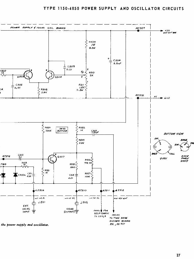
TYPE 1150-4050 POWER SUPPLY AND OSCILLATOR CIRCUITS
POWI!!'R SfJPPI..Y §' /OOKC OSC. 8o.<i~Rl>
--------------------------~~------------------~--------------~------~----~-------7----~· ~zo wH-.;H-ae
C503 0.01
2
RSII 1.5K
o.Jw
3
R509
IK 0.311/
R!SIO 2K
+ C504 ~.6JJ.F
______ _. ______________ +---------------------------~------------~----~ ~----~~r.~s._o_a ____ ~_s_K~~ ~N~ I
,t:/TSIS cg:o
R520
33DK
-ae~---~1~----~_,H
.T.tfl!J R519
II( ~---...-.!\,
EXT. IOOKC
INPVT "'""
RSZI IK
the power sgpply and oscillator.
Q507
R525 1001(
C512 0.01
R52(,
R52?
lOOK
A.T.S/0
IOOKC (OUTPIIT)-:
J 50"2.
I I I I I I BOTTOM YI£W
I &M
~-0"" :~, I J
I I
A.T.SII ""T.'SIZ I _____ _j
ltJOI(c. Tc~
SELF· CHECI(
TO S30/1 if; IOOKC
TO TINIE BASE
D/VI'DER BOAR'D B2. )so 401
27

Ol('
,-1
I I I I I
I I I I
C60!S
487
•
I AT.:
I I
l jAoweRj: I I I ('57.5 1 ,..s,u~"l
I I I I I
:I I
R!S05 IK
TYPE 1150-4050 POWER SUPPLY AND OSCILLATOR CIRCUITS
POWI!!'R SfJPPI..Y §' /OOKC OSC. 8o.<i~Rl>
C503 0.01
2
RSII 1.5K
o.Jw
3
R509
IK 0.3111
R!S/0 2K
+ C504 ~.6JJ.F
IIT.508 BK
LL-~---~-------------------~-----------~----------~-------------------~-------~--_J~-~--~--j_~~~ ~N~ I
M0501 I IW/MOTP.e
I I I
___ j
C50& fJ.OOI
R514 'l.SK
,t:/TSI5 cg:o
R520
33DK
--·------~~~----~~~
19.T.S09
RSZI 1K
Q507
C512
0.01
R52Z. IK
R623 2.21(
A.T.SII
I I I I I I BOTTOM YI£W
I &M
~-0"" :~, I J
I I
""T.'SIZ I I L -- ---- ---- --- --- --- --- --- -- -- -- ---~ --- --- -- --
_____ _j
"S.: RESfSTO.eS ftt.IV.4TT t.INL.E.SS .S.PEC'IFIE.O RESISTANCE IN OHMS t/Nt.ESS .S.PEC/..CIE.O
K•/000 OHMS M-1 MEGOHM CIIPRCITANCE //ALLIES ONE .411/.0 OYER IN PIC'OI'"If.I!'AOS, LESS TN/IN ONE INMIC.eOER.etii.OS UNLESS S.PEC'I/o/E.O
EXT. 100 KC INPVT """
J 501
Figure 4-10. Schematic diagram of the power sgpply and oscillator.
IOOKC (OUTPIIT)-:
ltJOI(c. To~
SELF· CHECI(
TO S30/1 if; IOOKC
TO TINIE BASE
D/VI'DER BOAR'D B2. )so 401
27

Transistor De Volts (Type) Terminal to Ground
Q101 E 14.6 (TR-19/2N1303) B 15.0
c 14.0
Ql02 E 14.1 (TR -19 /2N1303) B 14.0
c 14.0
Q103, Ql05, Q107, E 19.9 Ql09, QUI, Qll3, B 19.8 Qll5, Qll7, Qll9 c 19.9 (TR -19 /2Nl303)
+19.9
+14~ +10---
QI02,104 .... 120 BUSES!
Ql04, Ql06, Ql08, E 19.9 QllO, Qll2, Qll4, B 19.9 Qll6, Qll8 c 0 (TR -19 /2Nl303) +19.8--,
+I5.0---I QIOI, 103 .. .:.1.!_~_!3:.:.AS:.:E:..:S _ __J
Ql20 E 19.9 (TR -19 /2N1303) B 19.9
c 3.0 +19.91 .,.-- ----
+5--y
'(•14.1 v FOR 0102, 104, 106 .... 120 EMITTERS +14.6v FOR QIOI, 103, 105 .... 119 EMITTERS
Ql21 E 0 (TR-28/MM-487) B 0.5
c 0
Conditions of Measurement: ll IOv STEP
No input signal. Operate RESET switch to give a
display of "0".
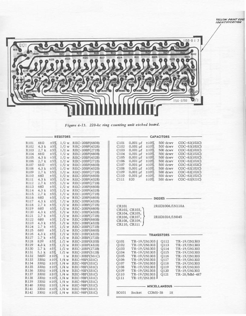
R101 680 R102 4.3 k Rl03 2.7 k R104 680 Rl05 4.3 k Rl06 2.7 k R107 680 R108 4.3 k Rl09 2.7 k RllO 680 R111 4.3 k Rll2 2.7 k R113 680 Rl14 4.3 k Rll5 2.7 k Rll6 680 Rll7 4.3 k Rll8 2.7 k Rll9 680 Rl20 4.3 k R121 2.7 k Rl22 6SO Rl 23 4.3 k Rl 24 2.7 k R125 680 R126 4.3 k Rl27 2.7 k Rl28 820 R129 4.3 k Rl30 2.7 k R131 5.1 k Rl32 5600 R133 3300 R134 3300 Rl35 3300 R136 3300 Rl37 3300 R138 3300 R139 3300 R140 3300 R141 3300 Rl42 3300
Figure 4-13. 220-kc ring counting unit etched board.
RESISTORS CAPACITORS
±5% 1/2 w REC-208F(6808) C101 0.001 IJf ±10% 500 dcwv COC-62(102C) ±5% 1/2 w REC-208F(4328) C102 0.001 fJf ±10% 500 dcwv COC-62(102C) ±5% 1/2 w REC- 208F(2728) Cl03 0.001 fJf ±10% 500 dcwv COC-62(102C) ±5% 1/2 w REC- 208F( 6808) Cl04 0.001 fJf ±10% 500 dcwv COC-62(102C) ±5% 1/2 w REC-208F(4328) Cl05 0.001 fJf ±10% 500 dcwv COC-62(102C) ±5% 1/2 w REC- 208F(2728) Cl06 0.001 fJf ±10% 500 dcwv COC-62(102C) ±5% 1/2 w REC-208F(6808) Cl07 0.001 fJf ±10% 500 dCWv COC-62(102C) ±5% 1/2 w REC-20BF(4328) Cl08 0.001 fJf ±10% 500 dcwv COC-62(102C) ±5% 1/2 w REC- 20BF(2728) C109 0.001 fJf ±10% 500 dcwv COC-62(102C) ±5% 1/2 w REC-20BF(6808) CllO 0.001 fJf ±10% 500 dcwv COC-62(102C) ±5% 1/2 w REC-208F( 4328) Clll 820 ±10% 500 dcwv COC-62(821C) ±5% 1/2 w REC-208F(272B) ±5% 1/2 w REC- 20BF(680B) ±5% 1 /2 w REC-20BF( 432B) ±5% 1/2 w REC- 208F(272B) ±5% 1/2 w REC- 20BF(680B) DIODES ±5% 1 /2 w REC-208F(4328) ±5% 1/2 w REC-20BF(2728) CRIOl 2RED1006/1Nll8A ±5% 1/2 w REC- 20BF( 6808)
CR102, CR103,} ±5% 1/2 w REC-208F(432B) CR104, CR105, ±5% 1/2 w REC- 20BF(2728) CR106, CR107, 2RED1016/1N645 ±5% 1/2 w REC-208F(6808) CR108, CR109, ±5% 1/2 w REC- 208F( 4328) CRllO, CRill ±5% 1/2 w REC-208F(2728) ±5% 1/2 w REC-208F(6808) ±5% 1/2 w REC- 20BF( 4328) TRANSISTORS ±5% 1/2 w REC-208F(2728) ±5% 1/2 w REC-208F(8208) Q101 TR-19/2Nl303 Q112 TR-19/2N1303 ±5% 1/2 w REC- 208F( 4328) Q102 TR-19/2N1303 Q113 TR-19/2Nl303 ±5% 1/2 w REC- 208F(2728) Ql03 TR-19 /2Nl303 Q114 TR-19/2Nl303 ±5% 1/2 w REC-208F(5128) Ql04 TR-19 /2Nl303 Q115 TR-19/2Nl303 ±10% lw REC-308F(561C) Ql05 TR-19/2Nl303 Q116 TR-19/2Nl303 ±10% l/4w REC-98F(331C) Ql06 TR-19/2Nl303 Q117 TR-19/2Nl303 ±10% 1/4 w REC-98F(331C) Q107 TR-19/2N1303 Q118 TR-19/2Nl303 ±10% 1/4 w REC-98F(331C) Q108 TR-19/2Nl303 Q119 TR-19/2N1303 ±10% 1/4 w REC-98F(331C) Ql09 TR -19 /2Nl303 Q120 TR-19/2Nl303 ±10% 1/4 w REC-98F(331C) QllO TR-19/2N1303 Ql21 TR-28/MM-487 ±10% 1/4 w REC-98F(331C) Qlll TR-19/2Nl303 ±10% 1/4 w REC-98F(331C) ±10% 1/4 w REC-98F(331C) MISCELLANEOUS ±10% l/4w REC-98F(331C) ±10% 1/4 w REC-98F(331C) SOlO I Socket CDMS-38 18
YELLOW PAIAIT EDGE ID£NTIFICHT/ON
+15V RESET BillS
D4~--------------------------~----------------4C----------------~----------------~r------------------~ SET ZERO
c3~--~~--~~--------------~~----------------~------------------1L----------------_J~----------------~ +15V RIO'l
4.3K.~--~----------~-----f~----------~-----J}-----------~-------~----------~------~-----------~------~
1NP1JT COVNT TRI+NSf:ER PIJLs£
Ri31 5.1 K
u ..-----J(~I----+-1 17 Clll
820
Cf.'IOI
}.IOTES:
RIO I
GB
I(EStS 7'0FIS f. W-'1 7'T UNLESS SPEC'/r/ELJ
REStS TIINCE IN OHMS UNLESS SPEC'/r/EO
K~IOOOS!..) Me: !MEGOHM C/'IPACt TIINCE r-'ALI.IE S ONE AND
OVE.R IN PICOFAR-'Il>S J LE 5S
THAN ONE IN 111 ICI?OFARAl>S VNLESS SPEC'/.F/.E£1
LAMPS o··-··9• P"'P.T OF
INDICATOR. IND-0300
BOTTOM VIEW
6 """ EM
CCLL
Figure 4-12. Schematic diagram for the 220.,
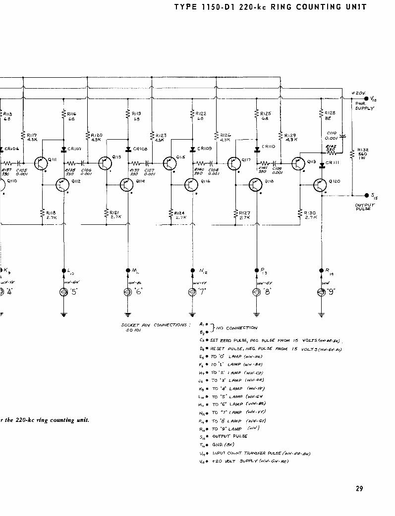
, K9 ~ w,V-YE
~ '4 ''5" '6''
f"
SOCKEr PIN so 10/
r the 220-kc ring counting unit.
TYPE 1150-01 220-kc RING COUNTING UNIT
CONNECTIONS
+20\1.
PWR. SUPPLY
R13Z. 5'-0 IW
..._ ____ ..__ ... s,5
tl,z p 1"3
"7' "B" \\911
.... .... A,•} CONNECTION NO Bz•
C3 e SET i!ERO PULSE, p0.S. PULSE FROM 15 VOLTS(W,..•II./!·8~<) .
D4e RESET PIJLSE,NEG. PVLSE FROM 15 VOLT~(WN'·If/I·J#)
£5 e TO "cf LAMP (w#·BI<l
F, • TO "1'' LAMP (w# ·8.1!)
H? e TO •z:• LAMP (W#·RP)
J 6 e TO "3" LAMP (w#-alf!)
1<9 • TO "4' LAMP (WH·YE}
L 10 e TO "5" LAMP (W#-t:;~
M., e TO 'G" LAMP (w#-81-)
N,.e TO '7" LflltiiP (w#-Vr)
P,,• lo "8 LAMP (WII-<¥Y)
R11
• TO "9" LAMP (w#)
515
• OuTPUT PULS£
T,•• GND. (BK)
U,,e INPUI COUNT TAIWSF£R PVLS£ {iv'#-RO·.SK)
v..• +'2.0 VOLT SUPPLY (w'#·triV·&e)
OUTPUT PULSE
29

TYPE 1150-01 220-kc RING COUNTING UNIT
+15V RESET BillS
D4~-------------------------r----------------4r----------------~----------------~---------------~----------------~----------------~----------------~----------------, SET ZERO
c3~--~~----~----------------~~----------------~~-----------------JI'------------------~------------~----~~-----------------1~-----------------"~-------------------~------------------~L-----------------, +15V RIO'l +20\1.
4.3K.---~----------~-----"I~----------~-----J~----------~------~-----------.------~-----------~------~----------~------J~--------·--~~----~~----------~----~~-----------~~-----'L-----------.-----JI'-~--~v,B
1NP1JT COVNT TRI+NSf:ER PIJLs£
R/31
5.1 K
U ..--.J(--+--H 17 C/11
820
Cf.'IOI
}.IOTES:
RIO I
GB
REsts roF<s f. W-" rr UNLESS SPEC'/r/ELJ
REStS TIINCE IN OHMS UNLESS SPEC'/r/EO
K~IOOOS!..) Me: !MEGOHM C/'IPACt TIINCE r-'ALI.IE .S ONE AND
OVE.R IN PICOFAR-'Il>S J LE 5S THAN ONE IN 111 ICI?OFARAl>S VNLESS SPEC'/F/.E£1
RI04 "a
LAMPS o··-··9• P"'RT OF
INDICATOR. IND-0300
BOTTOM VIEW
6 """ EM
CCLL
Figure 4-12. Schematic diagram fotr the 220-kc ring counting unit.
SOCKET PIN CONNECTIONS so 10/
Rl2'3 4.!11<
RI2.S ae
CliO o.ool
PWR. SUPPLY
R13Z. 5'-0 IW
._ _______ .._ _ _. s,5
A,•} NO CONNECTION Bz•
C3 • SET i!ERO PULSE, p0.S. PULSE FROM 15 VOLTS(W,oi·Jie·8~<) .
D4e RESET PIJLSE,NEG. PULSE FROM 15 VOL.T"~(WN'·If/1-J#)
£ 5 e TO "cf LAMP (w#·BI<l
F, • TO 'f' LAMP (W# ·8R)
H? e TO •z:• LAMP (W#·RP)
J6 e TO "3" LAMP (W#-alf!)
I(~ e TO "4' LAMP (W#-Yr)
L 10 e TO "5" LAMP (W#-t:;~
M11
e TO 'G" LAMP (WH·BI-)
N"e TO '7" Lfi/IIIP (w#-Vr)
P,,• lo •a LAMP (WII-<¥Y)
R11
• TO "9" LAMP (w#)
s,5
e OVTPlJT PULS£
T,•• GND. (BK)
U,,e INPUI COUNT TAIWSF£R PVLS£ {iv'#-RO·BK)
v..• +'2.0 VOLT SuPPLY (W#-triV·&e)
OUTPUT PULSE
29
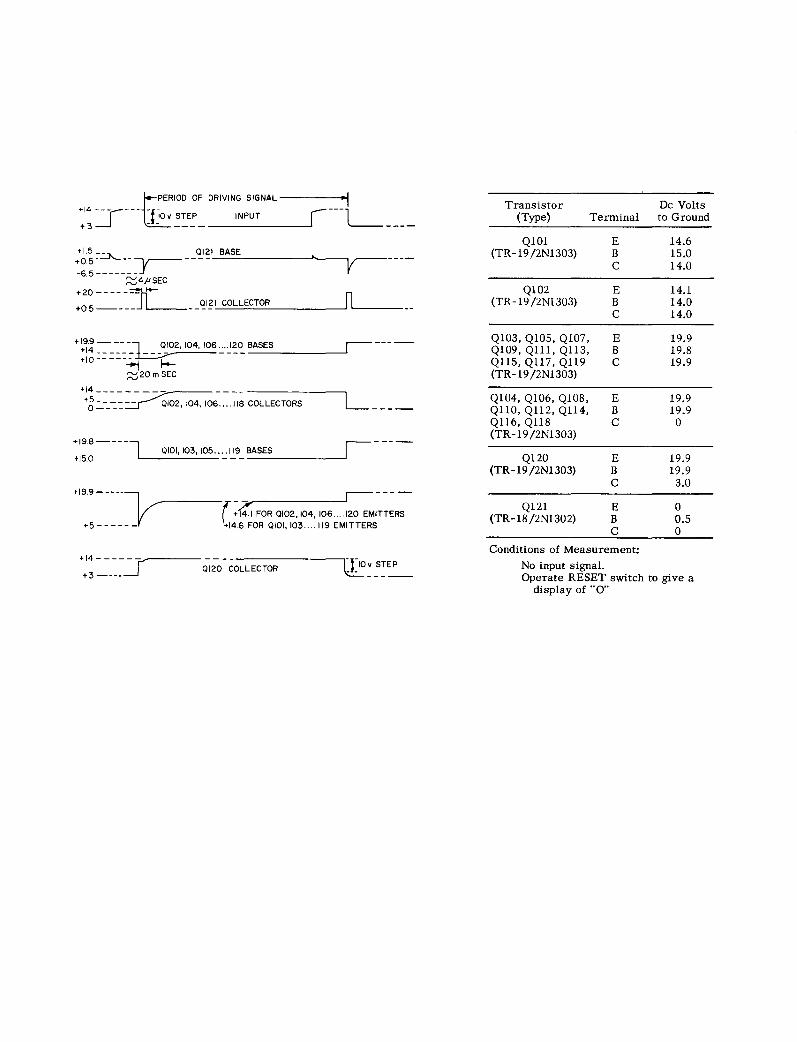
j--PERIOD OF DRIVING SIGNAL
::s---u~ov ~~E~- INPUT 1 L_ ___ _
+ 1.5 _ ~ --~~1-=.BA:..:.S:.:E:.._ ____ ......_ _ ___, +0.5-- --y---6•5 -----~4JISEC
-- n :~~=--~~]L___--~1~1 COLLECTOR L __ _
+~~l=-=--~~--l--~2, 104, 106~.~~<: BASES r------+lo-----~ f-
~2omsEc
+!g~=-~~~6~~.~1; COLLECTORS L ___ _
+19.8----l
+15.0 ,----0101,103, 105 .... 1198 _A_S_E_s _____ _..
+19.9-----y-- -~----
(:;;I FOR 0102, 104, 106 .... 120 EMITTERS +5------ +14.6 FOR 0101,103 .... 119 EMITTERS
+l4----r--0~;-0- ~OLLECTOR
+3 ----
Transistor De Volts (Type) Terminal to Ground
Q101 E 14.6 (TR -19/2N1303) B 15.0
c 14.0
Ql02 E 14.1 (TR -19/2N1303) B 14.0
c 14.0
Q103, Ql05, Q107, E 19.9 Q109, Q111, Qll3, B 19.8 Qll5, Ql17, Qll9 c 19.9 (TR -19/2N1303)
Q104, Ql06, Q108, E 19.9 QllO, Ql12, Qll4, B 19.9 Q116, Qll8 c 0 (TR -19/2N1303)
Ql20 E 19.9 (TR -19/2N1303) B 19.9
c 3.0
Q121 E 0 (TR-18/2N1302) B 0.5
c 0
Conditions of Measurement:
No input signal. Operate RESET switch to give a
display of "0"

R101 68 n R102 4.3 k R103 3.3 k R104 68 n R105 4.3 k R106 3.3 k R107 68 n R108 4.3 k R109 3. 3 k RllO 68 n Rll1 4.3 k Rll2 3.3 k Rll3 68 n Rll4 4.3 k Rll5 3.3 k Rll6 68 n Rll7 4.3 k Rll8 3.3 k Rll9 68 n R120 4.3 k Rl21 3.3 k R122 68 n R123 4.3 k R124 3.3 k R125 68 n R126 4.3 k Rl27 3.3 k R128 82 n Rl29 4.3 k R130 3.3 k Rl31 5.1 k R132 560 n Rl33 330 n R134 330 n Rl35 330 Q Rl36 330 Q Rl37 330 Q R138 330 n Rl39 330 n Rl40 330 Q Rl41 330 n Rl42 330 n
Figure 4-15. 30-_kc ring counting unit etched board.
RESISTORS CAPACITORS
±5% 1/2 w REC-20BF(680B) C101 0.0022 fJf ±10% 500 dcwv ±5% 1/2 w REC- 20BF( 432B) C102 0.0022 1-Lf ±10% 500 dcwv ±5% 1/2 w REC- 20BF(332B) C103 0.0022 1-Lf ±10% 500 dcwv ±5% 1/2 w REC-20B'F(680B) C104 0.0022 fJf ±10% 500 dcwv ±5% 1/2 w REC-20BF(432B) Cl05 0.0022 fJf ±10% 500 dcwv ±5% 1/2 w REC- 20BF(332B) C106 0.0022 1-Lf ±10% 500 dcwv ±5% 1/2 w REC-20BF(680B) C107 0.0022 fJf ±10% 500 dcwv ±5% 1/2 w REC-20BF(432B) C108 0.0022 1-Lf ±10% 500 dcwv ±5% 1/2 w REC-20BF(332B) C109 0.0022 fJf ±10% 500 dcwv ±5% 1/2 w REC- 20BF(680B) CllO 0.0022 1-Lf ±10% 500 dcwv ±5% 1/2 w REC-20BF(432B) Cll1 0.0033 fJf ±10% 500 dcwv ±5% 1/2 w REC-20BF(332B) ±5% 1/2 w REC-20BF(680B)
DIODE ±5% 1/2 w REC-20BF(432B) ±5% 1/2 w REC- 20BF(332B) CR102 2RED1016/1N645 ±5% 1/2 w REC-20BF(680B) thru ±5% 1/2 w REC-20BF(432B) CRill ±5% 1/2 w REC-20BF(332B) TRANSISTORS
±5% 1/2 w REC-20BF(680B) Q101 TR -19 /2N1303 Qll2 ±5% 1/2 w REC- 20BF( 432B) Q102 TR-19 /2N1303 Q113 ±5% 1/2 w REC-20BF(332B) Ql03 TR - 19 /2N1303 Qll4 ±5% 1/2 w REC-20BF(680B) Ql04 TR-19/2N1303 QllS ±5% 1/2 w REC-20BF(432B) Q105 TR -19 /2N1303 Qll6 ±5% 1/2 w REC-20BF(332B) Q106 TR-19/2N1303 Q117 ±5% 1/2 w REC- 20BF( 680B) Q107 TR-19/2N1303 Qll8 ±5% 1/2 w REC- 20BF( 432B) Q108 TR -19 /2Nl303 Qll9 ±5% 1/2 w REC-20BF(332B) Q109 TR-19/2N1303 Q120 ±5% 1/2 w REC-20BF(820B) QllO TR-19/2Nl303 Q121 ±5% 1/2 w REC- 20BF(432B) Qll1 TR-19/2Nl303 ±5% 1/2 w REC-20BF(332B) ±5% 1/2 w REC-20BF(512B)
MISCELLANEOUS ±10% 1w REC-30BF(561C) ±10% 1/4 w REC-9BF(331C) S0102 Socket CDMS-38, 18 ±10% 1 /4 w REC-9BF(331C) S0103 Socket CDMS-38, 18 ±10% 1/4 w REC-9BF(331C) S0104 Socket CDMS-38, 18 ±10% 1/4 w REC-9BF(331C) SOlOS Socket CDMS-38, 18 ±10% 1/4 w REC-9BF(331C) ±10% 1/4 w REC-9BF(331C) ±10% 1/4 w REC-9BF(331C) ±10% 1/4 w REC- 9BF(331C) ±10% 1/4 w REC-9BF(331C) ±10% 1/4 w REC-9BF(331C)
COC-62(222C) COC-62(222C) COC-62(222C) COC- 62(222C) COC-62(222C) COC- 62(222C) COC-62(222C) COC-62(222C) COC-62(222C) COC-62(222C) COC-62(332C)
TR-19/2Nl303 TR-19/2Nl303 TR - 19 /2Nl303 TR -19 /2N1303 TR-19/2N1303 TR- 19/2N1303 TR - 19 /2N1303 TR -19 /2N1303 TR-19/2N1303 TR-18/2Nl302
II! ED PAINT EDGE I IDENTIFIC'ATION
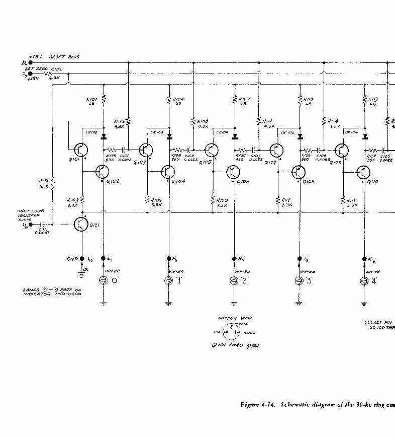
+15V RESET 811'15
~~----------------------------~--------------S~T ZE:RO /?102
c ·---"u'll\r-----.-------------------fi'----------~~-~~--'+15V 4.3K
R/3/
5./K
INpUr COUNT TR,tiNSFEP PvLS£
V ....-.J t--..__----iH 17 c Ill
0,0033
L/IM,OS o"- $i' A'IRT OF INDICI"'TOR IND-0300
RIO I t08
f' .. It v
sorroM VtE"W
~BAS£ EM~COLL
SOCKET PIN so IOZ-THR
Figure 4-14. Schematic diagram of the 30-kc ring cot

TYPE 1150-02 30-kc RING COUNTING UNIT
f;~ M
II
if ''6" '7"
~
SOCKET PIN CONNECTIONS ; SO 102- THRV 50105
·kc ring counting unit.
.,.
A,. J NO CONNE<.:.TIDN
Bz.•
C3. SET i!E:RO PVL5E1 POS, PVLSE FROM IS. VOLTS t'iW·BA!'·JI~)
0. • RESET PC/LS£, NEG, PVLSE ;C'AOM /5 VOLTS (WN'·IFN-6<.)
E5 • TO "0' LRMP (WN'-8K)
F, • TO'"!" LAMP (WH·IA!)
H1 e TO "2." LIIMP ( W#-RD)
J13. TO •3• LAMP (Wir'· tJR)
K9 e TO "4" LllMP (WN'· Y4)
PWR. Si./fJPLY
R/32 560
'""
·~--------._~.s
L,o • TO N5" L J!JMP (WN'- .;'10')
M,1e TO •c;" LAMP (WII·t!/,i.)
N1z• TO '7" LI'IMP (WK.- Vr)
P,1 • TO •a• LAMP (WN'· tO'}
R.., • TO •g• UIMP (WN'}
5 15 e OVTPUT PVL.SE.
T,, • GND. (-&K)
IS ovrPUr PULSE
U,, e l"NPUT COIJNT TRIINSF£R PCII..SE (WN'·>i!P·8A:)
V1e -e t-ZO VOl.. T SUPPL '( (Wir'·t;w-IU)
31

+15V RESET 811'15
~~-----------------------------.--------------S~T ZE:RO /?102
c e---'\/\Ar--~~---------------'['c___--------~~-~~--'+15V 4.3K
R/3/
5./K
INpUr COUNT TR,tiNSFEP PvLS£
v ......-J 1---+-------<1-1 17 c Ill
0,0033
L/IM,OS o"- !i' A'IRT OF INDICI"'TOR IND-0300
RIO I t08
TYPE 1150-02 30-kc RING COUNTING UNIT
f;~ M
II
if ''6"
sorroM VtEW
~BAS£ EM~COLL
T ~
SOCKET PIN CONNECTIONS ; SO 102- THRV 50105
Figure 4-14. Schematic diagram of the 30·kc ring counting unit.
.,.
A,. J NO CONNE<.:.TION
Bz.•
C3. SET i!ERO PVL5E1 POS, PVLSE FROM IS. VOLTS t'iW·BA!'·JI~)
0. • RESET PC/LS£, NEG. PVLSE )'"AOM /5 VOLTS (WN'·IFN-6<.)
E.5 • TO "0' t..,tiMP (WN'-8K)
F, • TO ··1• LAMP (WH·IA!)
H1 e TO '2." LIIMP (W#-RD)
J13. TO •3• LAMP (MY· tJR)
K9 e TO '4" LllMP (WN'· Y4)
PWR. Si./fJPLY
R/32 560
'""
,,.,._ ___ _..._ .... s
L1o• TONs" LIIIMP (WN'-t$"10')
M,1e TO •c;" LAMP (WII-8L)
N1z• TO '7"LI1MP (WK-Vr)
P,1 • TO •a• L.IIM P (WN'· tO')
Rl'l • TO '9' UIMP (WN'}
S 15 e OVTPUT PVL.SE.
T,, • GND. (-&K)
IS DVTPI)r PULSE
U, e l'NPUT COIJNT TRIINSF£R PCII.SE (WN'·>i!P·8A:)
V1& .. t-ZO VOl. T SUP PL.'( (WN'·t;A/-11#)

TYPE 1150-A INTERCONNECTION DIAGRAM
rotoli,D~
SOIOtJ,C-.1
AUX S0201
PHOTOELECTRIC PICKOFF
J303
WH-fiN•IL
AT l()fl
WH-BL-1/f ATI06
r· Ir~vrH-M-;R ol~,l L -5!--~~ u : ol$0$, IND (1"/fAMEJ
L IN-1111 - S0/011, S-Ill
'---'~~H::..·-=•~L-=-•::::1f:......-szol, I04R
: WH-fiN-111 A.T: 2011
If()
PROIIIIAM IOAifD OTIO
AT 104 WH-fiY-IL
PINH AT
106 WH-IL-IR
AT ,c 1 If' WH-fiY-IR S204 ,ILT
1/()
AT lOS WH-RD-.811 SMN. , IOZ/f
AT
SOhl/,1111' WH-RD-IJA IOZ
SIOI,I
ATIJotl
SOSOI,A-1 IK
S040I,D-4
~FIJOI,S/DE ~IIJOI,tl
M0501
(INOJ AT Ill
J~OI
e:J:$$01,$
@ssot,tl
J~02 r- 60SDI,A-I
INPUT
32
... A~
AT 10/
1 i
~,:'
WH·IY-IK . $1() 'I()"
(1+. ,4T
lOll
WH-fiN-IR
tiiOI,S .... (), SOSOI, II-IT
SOtiOI,A•
CHECK S~O/
TIME BASE INPIIT Dill AMP
~------ DECADES------~
stHOI $0.10/ BLANk SO/Oil S()/04 SONM SOl() I
ATZOII~Titlnlt WH·IY·fiN o/.101 c:,~ j ATIJII-
WH-111-IK . T c:::, ATIO.• ...... . . . . . . .
SOlO I
·A-I
.,_, •.. •c-~
WH-BN-IL ATI/1 • e ATifO "'eo-4et----t-1e--<•-•-4•,__ .. ,,.,. __ • ___ .... .,_ ..... D-4
•
• • • • • •
WH·VT-IK SIO/IOSI"
• eAT~
WH-VT-IR SIOI,IO!JF- AT~
DISPLAY TIME I SEC
( I •00
ENGifAIIINfl 1"011 5204
---- WH-IK TO INDICATO!f'o''-----.... - ---WH-111 TOINOICATOif't' ------
----- - ------wH-IfDTOIND/CATOif'l' ___ __,,.. ----------- WH-()trTOIND/CATOif~' ---....... ---------- WH-rE TOINDICATOif'4' ------------WH-.WTO IND/CATO!f)' ------- - ____. -------WH-IL TOINDICATOR'tl' ----- - ---M-11
----wH-IITTOINDICATOR'r'---__ __._ ---N-11
----WH-tiYTO INDICA TOll 'fl' ------- ---- --~----- WHTO INDICATOif'll''----
- - ---- -- _..R-14 WH-IN-IK
so101,s.i. L L~C:.:~:: 77 611-IT
ATIJOI . .. .. ........... •yll-11 tnf•fiN•IR
ATIJOT
5204 $2().1 N.lC: cw
lfi:SO~S,........,,..eJm:lllttZI p 20 I IOOKil e I Ar tJiN I .;- 1('1' l/oJe \ .. w'+-1e.,B,-l1fl.-$201,1 (fiND)
WH-IIT-GY I e..tJ Wli-fl'f-BL 1fT LT
NOTE.' SWITCH OPENS AT EJrrlfEME CLOCKWISE POSITION
COUNTING
Figure 4-16. Interconnection c
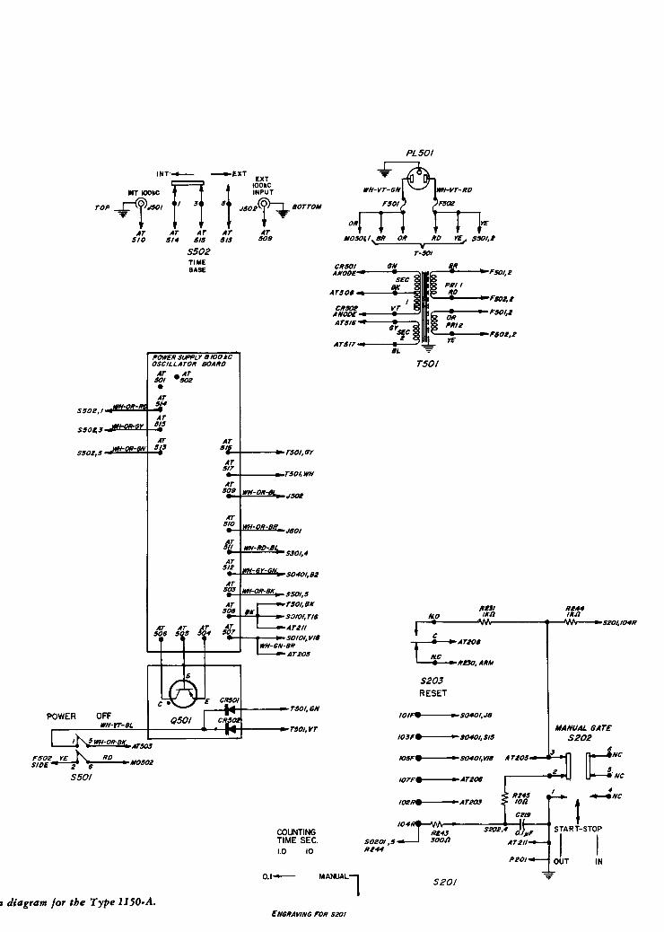
POWER
INT·- -J;XT
'"'-i<f-=' n ·t -1-+~"~
OFF
AT AT AT AT AT 510 514 515 51~ 5011
S502 TIME BASE
POWER S/IFPLY IJ 100 kC OSCILLATOR BOARO
tl, •fk • AT 54
e--¥'"'-'""-""<.., S!SOI, 5
TSOI,BK
e;.-+"=t-....., ... s.,JOI, Tits
ATZII
ATZ05
COUNTING TIME SEC. 1.0 10
J diagram for the Type 1150-A. ENGRAVING FOR $201
$0201,5 R244
PL501
It lUI IKIJ N.O
r-~~------~~--------~~~~-----SZOI,104R
RZIU IKIJ
c c:ATZOB
c lfZ~,ARM
S203 RESET
/Oif'e
IO~F·
IOSFe
107F.
102Re
104
• $0401,.!8
.. $0401,$15
• S0401,VIB
• AT206
• ATZCU
AT205
R245 10/J
RZ45 $202,4
~OOIJ
S201
MANUAL GATE 5202
2
n--'NC
U-----:Nc ., t -..Nc
SrRT-STl
OUT IN

GENERAL RADIO COMPANY WEST CONCORD, MASSACHUSETTS*
EMerson 9-4400 Mission 6-7400
5 ALE 5 ENGINEERING OFFICES
METROPOLITAN NEW YORK*
Broad Avenue at Linden Ridgefield, New Jersey Telephone N.Y. WOrth 4-2722
N.J. WHitney 3-3140
SYRACUSE Pickard Building East Molloy Road Syracuse 11, New York
Telephone GLenview 4-9323
PHILADELPHIA 1150 York Road Abington, Pennsylvania Telephone TUrner 7-8486
Philo., HAncock 4-7 419
WASHINGTON* and BALTIMORE
Rockville Pike at Wall Lane Rockville, Maryland Telephone 946-1600
ORLANDO 113 East Colonial Drive Orlando, Florida Telephone GArden 5-4671
• Repair services are available at these offices.
CHICAGO* 6605 West North Avenue Oak Park, Illinois Telephone VIllage 8-9400
CLEVELAND 5579 Pearl Road Cleveland 29, Ohio Telephone 886-0150
LOS ANGELES* 1 000 North Seward Street Los Angeles 38, California Telephone HOllywood 9-6201
SAN FRANCISCO 1186 Los Altos Avenue Los Altos, California Telephone WHitecliff 8-8233
DALLAS 2501-A West Mockingbird Lane Dallas 35, Texas Telephone FLeetwood 7-4031
TORONTO* 99 Floral Parkway Toronto 15, Ontario, Canada Telephone CHerry 7-2171
MONTREAL BRANCH Office 395 1255 Laird Boulevard Town of Mount Royal, Quebec, Canada Telephone 737-3673
General Radio Company (Overseas), Zurich, Switzerland Representatives in Principal Overseas Countries
Printed in USA