Embed Size (px)
Citation preview
Two-Dimensional van der Waals Materials Based Nonvolatile Memory Field-Effect
Transistors
Do Kyung Hwang
Center for Opto-Electronic Materials and Devices, Korea Institute of Science and Technology (KIST)
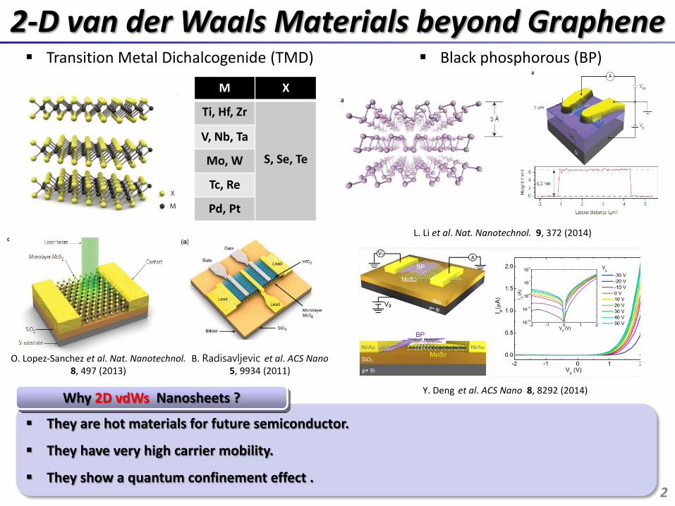
2-D van der Waals Materials beyond Graphene
2
Transition Metal Dichalcogenide (TMD) Black phosphorous (BP)
M X
Ti, Hf, Zr
S, Se, Te
V, Nb, Ta
Mo, W
Tc, Re
Pd, Pt
They are hot materials for future semiconductor.
They have very high carrier mobility.
They show a quantum confinement effect .
Why 2D vdWs Nanosheets ?
O. Lopez-Sanchez et al. Nat. Nanotechnol. 8, 497 (2013)
B. Radisavljevic et al. ACS Nano 5, 9934 (2011)
L. Li et al. Nat. Nanotechnol. 9, 372 (2014)
Y. Deng et al. ACS Nano 8, 8292 (2014)
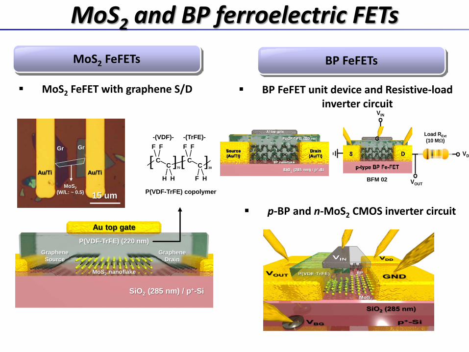
MoS2 and BP ferroelectric FETs MoS2 FeFETs BP FeFETs
VD
Load RExt(10 MΩ)
VIN
VOUTBFM 02
BP FeFET unit device and Resistive-load inverter circuit
p-BP and n-MoS2 CMOS inverter circuit
MoS2 FeFET with graphene S/D
Au top gateP(VDF-TrFE) (220 nm)
MoS2 nanoflake
GrapheneSource
GrapheneDrain
SiO2 (285 nm) / p+-Si
[ ]CC
F F
H H
[ ]CC
F F
F H
70 30
-(VDF)- -(TrFE)-
P(VDF-TrFE) copolymer15 um
Gr Gr
Au/Ti Au/Ti
MoS2(W/L: ~ 0.5)
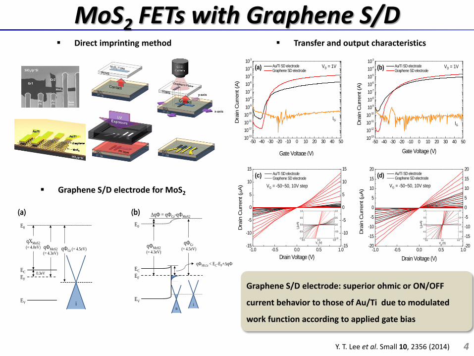
MoS2 FETs with Graphene S/D
4
x-axis
y-axis
5um
Gr1Gr2
MoS2
Au/Ti
Au/Ti
SiO2/p+Si
(a) (b)
E0
qХMoS2(= 4.0eV)
ECEF
EV
0.3eV
qФGr (= 4.5eV)
i
qФMoS2(= 4.3eV)
E0
ECEF
EVi
n
qФSB,Gr < EC-EF+∆qФ
∆qФ = qФGr-qФMoS2
qФMoS2(= 4.3eV)
qФGr (= 4.5eV)
-50 -40 -30 -20 -10 0 10 20 30 40 5010-13
10-12
10-11
10-10
10-9
10-8
10-7
10-6
10-5
10-4
10-3
Gate Voltage (V)
Dra
in C
urre
nt (A
)
Au/Ti SD electrode Graphene SD electrode
-1.0 -0.5 0.0 0.5 1.0-15
-10
-5
0
5
10
15
-15
-10
-5
0
5
10
15
Drain Voltage (V)
Dra
in C
urre
nt (µ
A)
Au/Ti SD electrode Graphene SD electrode
-0.5 0.0 0.5-1.0
-0.5
0.0
0.5
1.0
-1.0
-0.5
0.0
0.5
1.0
VD (V)
I D(µ
A)
VD = 1V
VG = -50~50, 10V step
IG
(a)
(c)
-1.0 -0.5 0.0 0.5 1.0-20
-15
-10
-5
0
5
10
15
20
-20
-15
-10
-5
0
5
10
15
20
Drain Voltage (V)
Dra
in C
urre
nt (µ
A)
Au/Ti SD electrode Graphene SD electrode
-50 -40 -30 -20 -10 0 10 20 30 40 5010-13
10-12
10-11
10-10
10-9
10-8
10-7
10-6
10-5
10-4
10-3
Au/Ti SD electrode Graphene SD electrode
Gate Voltage (V)
Dra
in C
urre
nt (A
)
-0.5 0.0 0.5-1.0
-0.5
0.0
0.5
1.0
-1.0
-0.5
0.0
0.5
1.0
I D(µ
A)
VD (V)
(b)
(d)
VD = 1V
VG = -50~50, 10V step
IG
Direct imprinting method Transfer and output characteristics
Graphene S/D electrode for MoS2
Y. T. Lee et al. Small 10, 2356 (2014)
Graphene S/D electrode: superior ohmic or ON/OFF
current behavior to those of Au/Ti due to modulated
work function according to applied gate bias
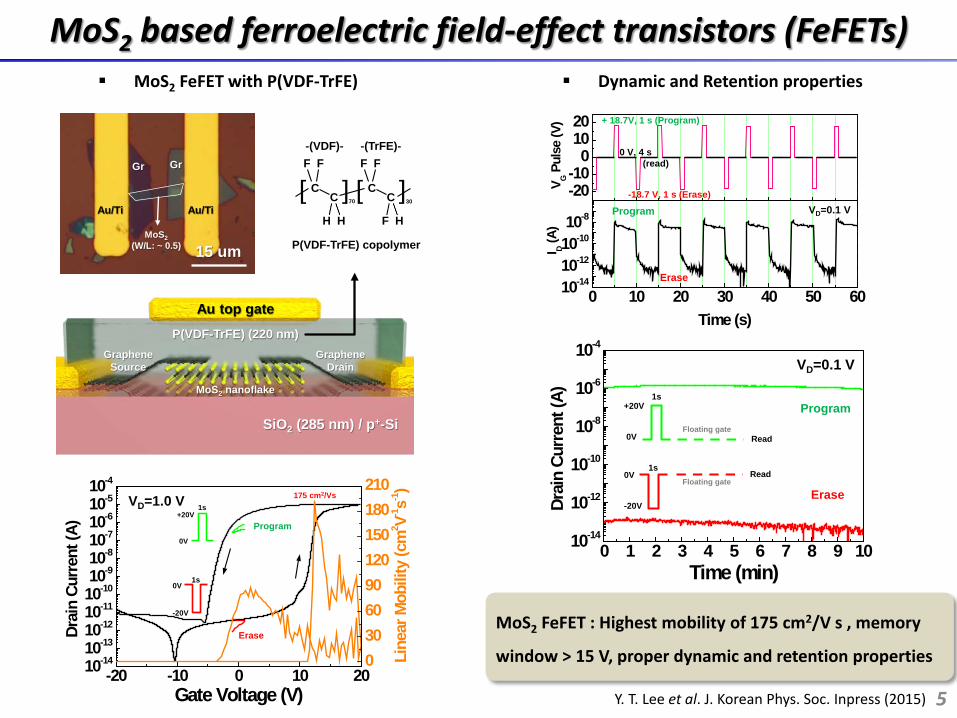
MoS2 based ferroelectric field-effect transistors (FeFETs)
5
Au top gateP(VDF-TrFE) (220 nm)
MoS2 nanoflake
GrapheneSource
GrapheneDrain
SiO2 (285 nm) / p+-Si
[ ]CC
F F
H H
[ ]CC
F F
F H
70 30
-(VDF)- -(TrFE)-
P(VDF-TrFE) copolymer15 um
Gr Gr
Au/Ti Au/Ti
MoS2(W/L: ~ 0.5)
Y. T. Lee et al. J. Korean Phys. Soc. Inpress (2015)
MoS2 FeFET with P(VDF-TrFE)
0 1 2 3 4 5 6 7 8 9 1010-14
10-12
10-10
10-8
10-6
10-4
Drai
n Cu
rrent
(A)
Time (min)
Erase
Program
0V
-20V
1sRead
Floating gate
1s+20V
0V ReadFloating gate
VD=0.1 V
0 10 20 30 40 50 6010-1410-1210-1010-8
-20-10
01020
I D (A)
Time (s)
V G Pul
se (V
)
Erase
Program VD=0.1 V
+ 18.7V, 1 s (Program)
-18.7 V, 1 s (Erase)
0 V, 4 s(read)
-20 -10 0 10 2010-1410-1310-1210-1110-1010-910-810-710-610-510-4
Line
ar M
obili
ty (c
m2 V-1
s-1)
Drai
n Cu
rrent
(A)
Gate Voltage (V)
0306090120150180210
VD=1.0 V 175 cm2/Vs
Erase
Program
1s+20V
0V
0V
-20V
1s
Dynamic and Retention properties
MoS2 FeFET : Highest mobility of 175 cm2/V s , memory
window > 15 V, proper dynamic and retention properties
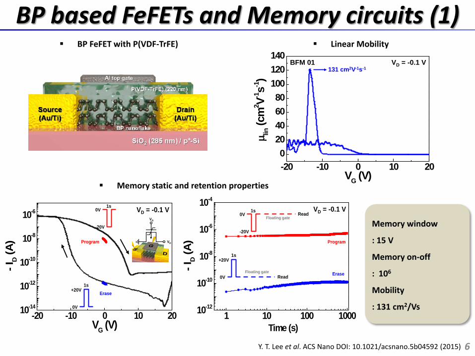
BP based FeFETs and Memory circuits (1)
6
-20 -10 0 10 2010-14
10-12
10-10
10-8
10-6
- ID (
A)
VG (V)
VD = -0.1 V
Program
Erase1s
+20V
0V
0V
-20V
1s
VG
VD
1 10 100 100010-12
10-10
10-8
10-6
10-4- I
D (A)
Time (s)
0V
-20V
1s ReadFloating gate
VD = -0.1 V
1s+20V
0V Read
Program
EraseFloating gate
Y. T. Lee et al. ACS Nano DOI: 10.1021/acsnano.5b04592 (2015)
-20 -10 0 10 200
20406080
100120140
µ lin (c
m2 V-1
s-1)
VG (V)
VD = -0.1 VBFM 01131 cm2V-1s-1
Memory window
: 15 V
Memory on-off
: 106
Mobility
: 131 cm2/Vs
BP FeFET with P(VDF-TrFE) Linear Mobility
Memory static and retention properties
BP based FeFETs and Memory circuits (2)
7
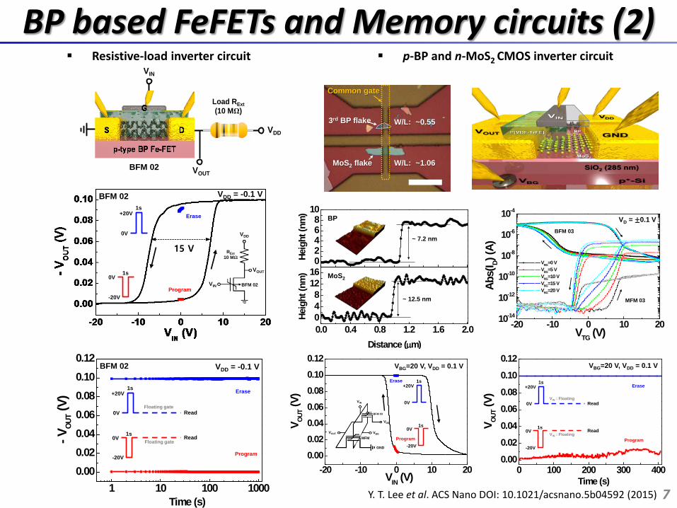
VDD
Load RExt(10 MΩ)
VIN
VOUTBFM 02
W/L: ~0.55
W/L: ~1.06
3rd BP flake
MoS2 flake
Common gate
Y. T. Lee et al. ACS Nano DOI: 10.1021/acsnano.5b04592 (2015)
VDD = -0.1 V
VIN
VOUT
VDD
RExt10 MΩ
BFM 02Program
Erase1s
+20V
0V
0V
-20V
1s
BFM 02
15 V
1 10 100 10000.000.020.040.060.080.100.12
- VOU
T (V)
Time (s)
0V
-20V
1s ReadFloating gate
Program
Erase1s+20V
0V ReadFloating gate
VDD = -0.1 VBFM 02
Resistive-load inverter circuit p-BP and n-MoS2 CMOS inverter circuit
-20 -10 0 10 2010-14
10-12
10-10
10-8
10-6
10-4
VBG=0 V VBG=5 V VBG=10 V VBG=15 V VBG=20 V
Abs (
I D) (A
)
VTG (V)
VD = ±0.1 VBFM 03
MFM 03
-20 -10 0 10 200.000.020.040.060.080.100.12
V OUT (
V)
VIN (V)
Program
Erase 1s+20V
0V
0V
-20V
1s
VBG=20 V, VDD = 0.1 V
VDD
VOUT
BFM 03
MFMVBG
GND
VIN
0 100 200 300 4000.000.020.040.060.080.100.12
Time (s)V OU
T (V)
0V
-20V
1s ReadVIN : Floating
Program
Erase1s
+20V
0V ReadVIN : Floating
VBG=20 V, VDD = 0.1 V
02468
10
Heig
ht (n
m)
0.0 0.4 0.8 1.2 1.6 2.0048
1216
Distance (µm)
Heig
ht (n
m)
~ 7.2 nm
~ 12.5 nm
BP
MoS2
Summary
8
We demonstrate the high performance MoS2 based nonvolatile memory
transistors
High performance, clear memory window, proper dynamic and retention properties
Papers: Y. T. Lee et al. Small 10, 2356 (2014) and J. Korean Phys. Soc Inpress (2015)
We also demonstrate few-layered BP-based nonvolatile memory transistors and
more advanced memory circuits.
Unit device, resistive-load inverter, and CMOS inverter combined with MoS2
Paper: Y. T. Lee et al. ACS Nano DOI: 10.1021/acsnano.5b04592 (2015)