Embed Size (px)
Citation preview
Strong interlayer coupling in van der Waalsheterostructures built from single-layer chalcogenidesHui Fanga,b, Corsin Battagliaa,b, Carlo Carraroc, Slavomir Nemsakb,d, Burak Ozdole,f, Jeong Seuk Kanga,b,Hans A. Bechtelg, Sujay B. Desaia,b, Florian Kronasth, Ahmet A. Unalh, Giuseppina Contib,d, Catherine Conlonb,d,Gunnar K. Palssonb,d, Michael C. Marting, Andrew M. Minore,f, Charles S. Fadleyb,d, Eli Yablonovitcha,b,1,Roya Maboudianc, and Ali Javeya,b,1
Departments of aElectrical Engineering and Computer Sciences, cChemical and Biomolecular Engineering, and eMaterials Science and Engineering, Universityof California, Berkeley, CA 94720; bMaterials Sciences Division, fNational Center for Electron Microscopy, and gAdvanced Light Source, Lawrence BerkeleyNational Laboratory, Berkeley, CA 94720; dDepartment of Physics, University of California, Davis, CA 95616; and hHelmholtz-Zentrum Berlin für Materialienund Energie GmbH, D-12489 Berlin, Germany
Contributed by Eli Yablonovitch, March 24, 2014 (sent for review March 10, 2014)
Semiconductor heterostructures are the fundamental platform formany important device applications such as lasers, light-emittingdiodes, solar cells, and high-electron-mobility transistors. Analo-gous to traditional heterostructures, layered transition metaldichalcogenide heterostructures can be designed and built byassembling individual single layers into functional multilayerstructures, but in principle with atomically sharp interfaces, nointerdiffusion of atoms, digitally controlled layered components,and no lattice parameter constraints. Nonetheless, the optoelec-tronic behavior of this new type of van der Waals (vdW) semi-conductor heterostructure is unknown at the single-layer limit.Specifically, it is experimentally unknown whether the opticaltransitions will be spatially direct or indirect in such hetero-bilayers. Here, we investigate artificial semiconductor heterostruc-tures built from single-layer WSe2 and MoS2. We observe a largeStokes-like shift of ∼100 meV between the photoluminescencepeak and the lowest absorption peak that is consistent with a typeII band alignment having spatially direct absorption but spatiallyindirect emission. Notably, the photoluminescence intensity of thisspatially indirect transition is strong, suggesting strong interlayercoupling of charge carriers. This coupling at the hetero-interfacecan be readily tuned by inserting dielectric layers into the vdWgap, consisting of hexagonal BN. Consequently, the generic natureof this interlayer coupling provides a new degree of freedom inband engineering and is expected to yield a new family of semi-conductor heterostructures having tunable optoelectronic proper-ties with customized composite layers.
MoS2-WSe2 heterostructure | Moiré pattern | charge transfer |exciton relaxation | rectifying
Two-dimensional layered transition metal dichalcogenide(TMDC) semiconductors such as MoS2 and WSe2 have
established themselves as strong contenders for next-generationelectronics and optoelectronics (1–6) and are promising buildingblocks for novel semiconductor heterostructures (7–11). Con-ventional heterostructures are mainly based on group IV, III-V,or II-VI semiconductors with covalent bonding between atomsat the hetero-interface. Owing to atomic interdiffusion duringgrowth, the resulting atomic-scale interface roughness and com-position variation at the hetero-interface inevitably smear thedensity of states profile and consequently compromise the per-formance of these heterostructures, especially as the film thick-nesses are reduced toward a single atomic layer. In addition, thechoice of material components for conventional heterostructuresis strongly dictated by lattice mismatch.In TMDCs, however, individual layers are held together by van
der Waals (vdW) forces, without surface dangling bonds (12).Semiconductor heterostructures built up from monolayer TMDCswould in principle offer atomically regulated interfaces and therebysharp band edges. Theoretical studies have predicted different
electronic structures and optical properties from TMDC hetero-bilayers (13–17); however, to date there have been no experi-mental results. Whereas previous experimental efforts havefocused on graphene-based layered heterostructures (8–11, 18–26), we present an experimental study on the electronic in-terlayer interaction in a heterostructure built from two single-layer TMDC semiconductors, namely, MoS2 and WSe2. Thehetero-bilayers are characterized by transmission electron mi-croscopy, X-ray photoelectron microscopy, electron transportstudies, and optical spectroscopy to elucidate the band alignments,optoelectronic properties, and the degree of the electronic layercoupling in this novel material system.The fabrication of WSe2/MoS2 hetero-bilayers was realized by
stacking individual monolayers on top of each other (see SIMethods for details). Fig. 1A shows an illustration of the hetero-bilayer, and Fig. 1B displays the corresponding optical micro-scope image of a WSe2/MoS2 hetero-bilayer on a Si substratewith 260-nm thermally grown SiO2. Owing to the 3.8% latticemismatch, estimated from the bulk lattice constants (12), as wellas the unregulated, but in principle controllable, angular align-ment (ϕ) between the constituent layers, the heterostructurelattice forms a moiré pattern, clearly visible in the high-resolu-tion transmission electron microscopy (HRTEM) image in Fig.1C. The HRTEM image displays the boundary region between
Significance
A new class of heterostructures consisting of layered transitionmetal dichalcogenide components can be designed and built byvan der Waals (vdW) stacking of individual monolayers intofunctional multilayer structures. Nonetheless, the optoelec-tronic properties of this new type of vdW heterostructure areunknown. Here, we investigate artificial semiconductor heter-ostructures built from single-layer WSe2 and MoS2. We observespatially direct absorption but spatially indirect emission in thisheterostructure, with strong interlayer coupling of charge car-riers. The coupling at the hetero-interface can be readily tunedby inserting hexagonal BN dielectric layers into the vdW gap.The generic nature of this interlayer coupling is expected to yielda new family of semiconductor heterostructures having tunableoptoelectronic properties through customized composite layers.
Author contributions: H.F., C. Carraro, R.M., and A.J. designed research; H.F., C. Carraro,S.N., B.O., J.S.K., H.A.B., S.B.D., F.K., A.A.U., G.C., C. Conlon, G.K.P., and M.C.M. performedresearch; H.F., C.B., C. Carraro, S.N., B.O., G.C., A.M.M., C.S.F., E.Y., R.M., and A.J. analyzeddata; and H.F., C.B., and A.J. wrote the paper.
The authors declare no conflict of interest.
Freely available online through the PNAS open access option.1To whom correspondence may be addressed. E-mail: [email protected] or [email protected].
This article contains supporting information online at www.pnas.org/lookup/suppl/doi:10.1073/pnas.1405435111/-/DCSupplemental.
6198–6202 | PNAS | April 29, 2014 | vol. 111 | no. 17 www.pnas.org/cgi/doi/10.1073/pnas.1405435111
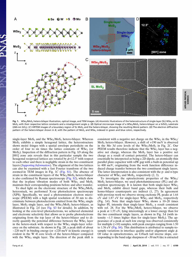
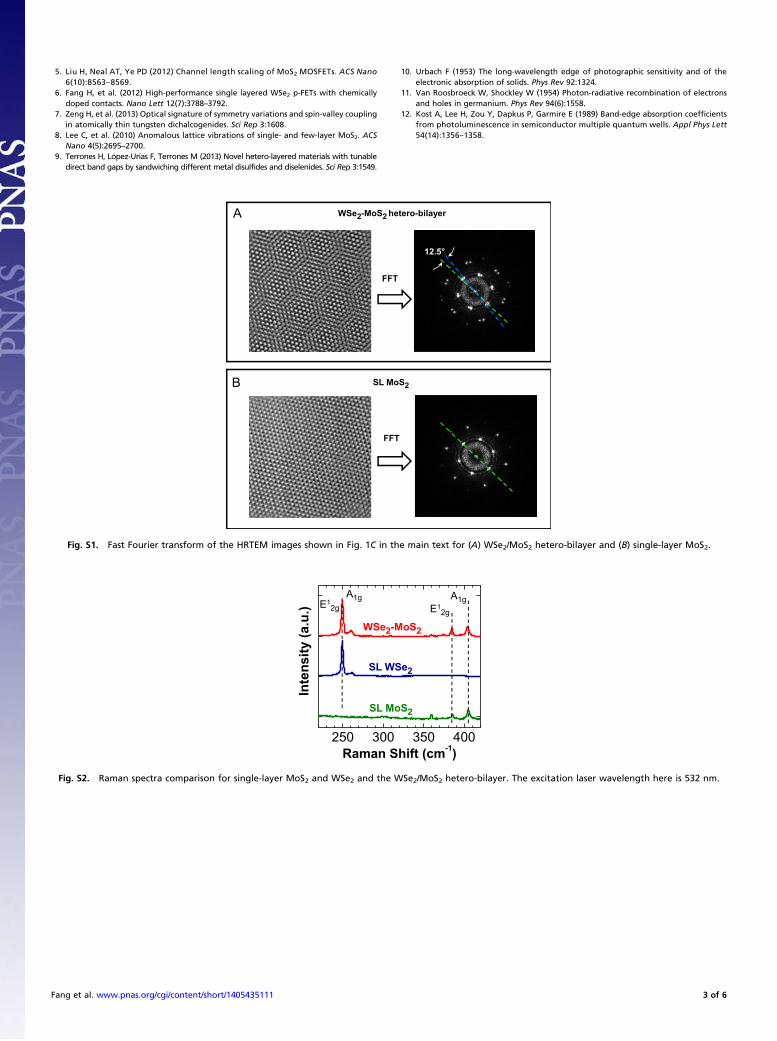
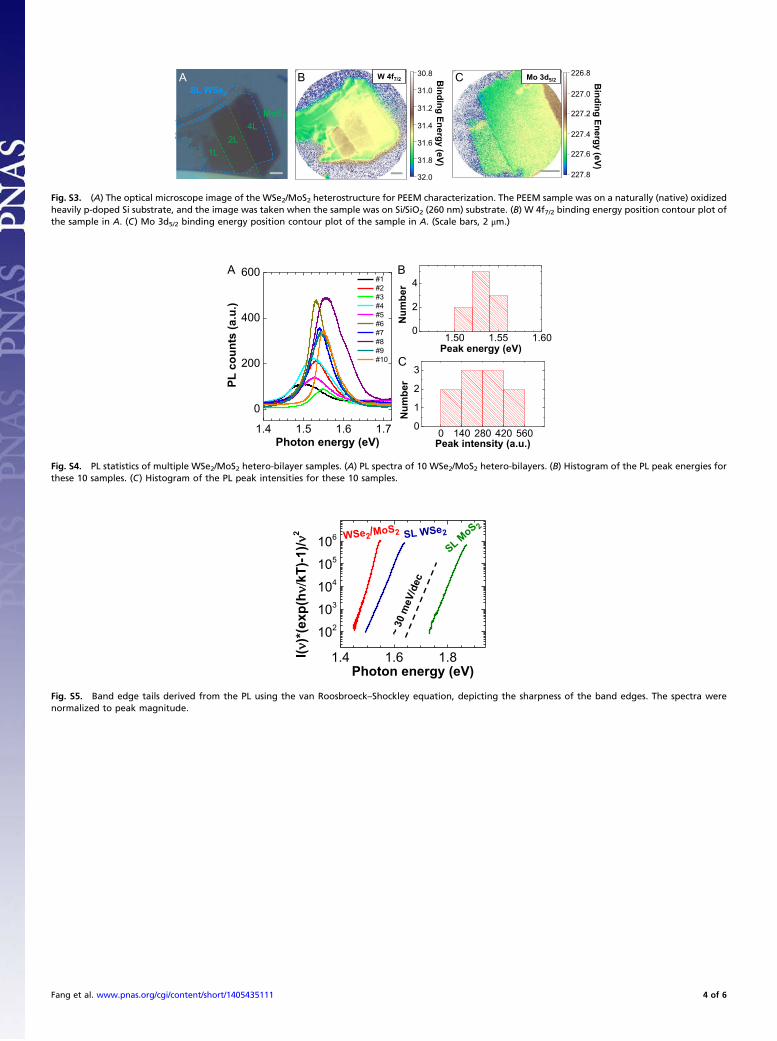
single-layer MoS2 and the WSe2/MoS2 hetero-bilayer. WhereasMoS2 exhibits a simple hexagonal lattice, the heterostructureshows moiré fringes with a spatial envelope periodicity on theorder of four to six times the lattice constants of WSe2 (orMoS2). Inspection of the diffraction pattern in Fig. 1D along the[001] zone axis reveals that in this particular sample the twohexagonal reciprocal lattices are rotated by ϕ=12.5° with respectto each other and there is negligible strain in the two constituentlayers (Supporting Information). The alignment of the two latticescan also be examined with a fast Fourier transform of the twozoomed-in TEM images in Fig. 1C (Fig. S1). The absence ofstrain in the constituent layers of the WSe2/MoS2 hetero-bilayeris also confirmed by Raman spectroscopy (Fig. S2), which showthat the in-plane vibration modes of both WSe2 and MoS2maintain their corresponding positions before and after transfer.To shed light on the electronic structure of the WSe2/MoS2
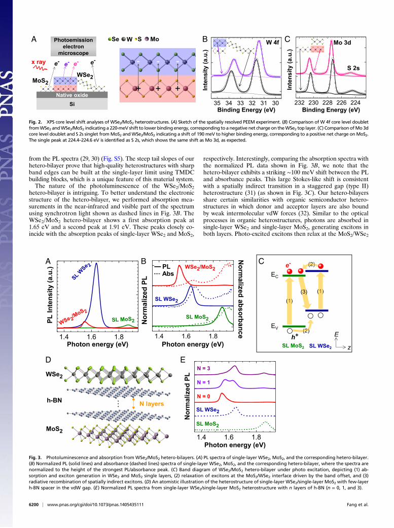
heterostack, we performed X-ray photoelectron spectroscopy(XPS). Specifically, we used a photoemission electron micro-scope (PEEM) with a high spatial resolution of 30 nm to dis-criminate between photoelectrons emitted from the WSe2 singlelayer, MoS2 single layer, and the WSe2/MoS2 hetero-bilayer, asillustrated in Fig. 2A (see Fig. S3 for details). In addition, bylooking at the core-level photoelectrons, we achieved elementaland electronic selectivity that allows us to probe photoelectronsoriginating from the top layer of the hetero-bilayer and to di-rectly quantify the potential difference between the WSe2 layerin the hetero-stack with respect to the WSe2 single-layer refer-ence on the substrate. As shown in Fig. 2B, a peak shift of about−220 meV in binding energy (or +220 meV in kinetic energy) isevident in the W 4f core levels of the hetero-bilayer comparedwith the WSe2 single layer. The direction of the peak shift is
consistent with a negative net charge on the WSe2 in the WSe2/MoS2 hetero-bilayer. However, a shift of +190 meV is observedin the Mo 3d core levels of the WSe2/MoS2 in Fig. 2C. OurPEEM results therefore indicate that the WSe2 layer has a neg-ative net charge, whereas the MoS2 layer has a positive netcharge as a result of contact potential. The hetero-bilayer canessentially be interpreted as being a 2D dipole, an atomically thinparallel plate capacitor with vdW gap with a built-in potential upto 400 meV, originating from the work function difference in-duced charge transfer between the two constituent single layers.The latter interpretation is also consistent with the p- and n-typecharacter of WSe2 and MoS2, respectively (2, 3).To investigate the optoelectronic properties of the WSe2/
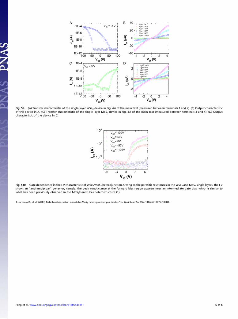
MoS2 hetero-bilayer, we used photoluminescence (PL) and ab-sorption spectroscopy. It is known that both single-layer WSe2and MoS2 exhibit direct band gaps, whereas their bulk andhomo-bilayer counterparts are indirect (1, 27). In agreementwith previous work we observe strong excitonic PL peaks at 1.64eV and 1.87 eV for single-layer WSe2 and MoS2, respectively(Fig. 3A). Note that single-layer WSe2 shows a 10–20 timeshigher PL intensity than single-layer MoS2, a result consistentwith ref. 28. For the WSe2/MoS2 hetero-bilayer, we observea peak at 1.55 eV, lying interestingly at a lower energy than forthe two constituent single layers, as shown in Fig. 3A (with in-tensity ∼1.5 times higher than for single-layer MoS2). The ap-pearance of a peak at such low energy was observed consistentlyfor multiple (>10) samples, with peak energies ranging from 1.50to 1.56 eV (Fig. S4). This distribution is attributed to sample-to-sample variations in interface quality and/or alignment angle ϕ.Of value in optoelectronics, an Urbach tail inverse slope, cor-responding to the band edge sharpness of ∼30 meV/dec is extracted
Single-layer MoS2
Single-layer WSe2
3 μm
x
z
WSe S Mo
x
y
12.5°
110110
5 nm
WSe2/MoS2hetero-bilayer
WSe2
WSe2/MoS2
SL MoS2
MoS2
[001] zone
A B
C
D
Fig. 1. WSe2/MoS2 hetero-bilayer illustration, optical image, and TEM images. (A) Atomistic illustrations of the heterostructure of single-layer (SL) WSe2 on SLMoS2 with their respective lattice constants and a misalignment angle ϕ. (B) Optical microscope image of a WSe2/MoS2 hetero-bilayer on a Si/SiO2 substrate(260-nm SiO2). (C) HRTEM images of a boundary region of SL MoS2 and the hetero-bilayer, showing the resulting Moiré pattern. (D) The electron diffractionpattern of the hetero-bilayer shown in B, with the pattern of MoS2 and WSe2 indexed in green and blue colors, respectively.
Fang et al. PNAS | April 29, 2014 | vol. 111 | no. 17 | 6199
APP
LIED
PHYS
ICAL
SCIENCE
S
from the PL spectra (29, 30) (Fig. S5). The steep tail slopes of ourhetero-bilayer prove that high-quality heterostructures with sharpband edges can be built at the single-layer limit using TMDCbuilding blocks, which is a unique feature of this material system.The nature of the photoluminescence of the WSe2/MoS2
hetero-bilayer is intriguing. To better understand the electronicstructure of the hetero-bilayer, we performed absorption mea-surements in the near-infrared and visible part of the spectrumusing synchrotron light shown as dashed lines in Fig. 3B. TheWSe2/MoS2 hetero-bilayer shows a first absorption peak at1.65 eV and a second peak at 1.91 eV. These peaks closely co-incide with the absorption peaks of single-layer WSe2 and MoS2,
respectively. Interestingly, comparing the absorption spectra withthe normalized PL data shown in Fig. 3B, we note that thehetero-bilayer exhibits a striking ∼100 meV shift between the PLand absorbance peaks. This large Stokes-like shift is consistentwith a spatially indirect transition in a staggered gap (type II)heterostructure (31) (as shown in Fig. 3C). Our hetero-bilayersshare certain similarities with organic semiconductor hetero-structures in which donor and acceptor layers are also boundby weak intermolecular vdW forces (32). Similar to the opticalprocesses in organic heterostructures, photons are absorbed insingle-layer WSe2 and single-layer MoS2, generating excitons inboth layers. Photo-excited excitons then relax at the MoS2/WSe2
A
Native oxideSi
Photoemission electron
microscope
e-
+ + +
- - -
WSe S Mo
x ray e- e- e-
WSe2MoS2
B C
35 34 33 32 31 30
). u.a(ytisnetnI
Binding Energy (eV)232 230 228 226 224
). u.a(yt is netnI
Binding Energy (eV)
W 4f Mo 3d
S 2s
Fig. 2. XPS core level shift analyses of WSe2/MoS2 heterostructures. (A) Sketch of the spatially resolved PEEM experiment. (B) Comparison of W 4f core level doubletfromWSe2 andWSe2/MoS2 indicating a 220-meV shift to lower binding energy, corresponding to a negative net chargeon theWSe2 top layer. (C) Comparison ofMo3dcore level doublet and S 2s singlet fromMoS2 andWSe2/MoS2 indicating a shift of 190 meV to higher binding energy, corresponding to a positive net charge onMoS2.The single peak at 224.4–224.6 eV is identified as S 2s, which shows the same shift as Mo 3d, as expected.
1.4 1.6 1.8
).u.a(ytisnetnI
LP
Photon energy (eV)
1.4 1.6 1.8
LPdezila
mroN
Photon energy (eV)
1.4 1.6 1.8Photon energy (eV)
LPdezila
mr oN
e cna
b ro s
bade
zila
mro
N
SL MoS2
SL WSe2
WSe2/MoS2
SL MoS2
SL WSe2
…
N = 3
N = 1
N = 0N la ers
WSe2
MoS2
h-BN
SL MoS2 SL WSe2
E
z
e-
h+EV
EC
(1)
(1)
(2)
(2)
(3)
(1)
(1)
(2)
(2)
PLAbs
A B C
D E
y
Fig. 3. Photoluminescence and absorption from WSe2/MoS2 hetero-bilayers. (A) PL spectra of single-layer WSe2, MoS2, and the corresponding hetero-bilayer.(B) Normalized PL (solid lines) and absorbance (dashed lines) spectra of single-layer WSe2, MoS2, and the corresponding hetero-bilayer, where the spectra arenormalized to the height of the strongest PL/absorbance peak. (C) Band diagram of WSe2/MoS2 hetero-bilayer under photo excitation, depicting (1) ab-sorption and exciton generation in WSe2 and MoS2 single layers, (2) relaxation of excitons at the MoS2/WSe2 interface driven by the band offset, and (3)radiative recombination of spatially indirect excitons. (D) An atomistic illustration of the heterostructure of single-layer WSe2/single-layer MoS2 with few-layerh-BN spacer in the vdW gap. (E) Normalized PL spectra from single-layer WSe2/single-layer MoS2 heterostructure with n layers of h-BN (n = 0, 1, and 3).
6200 | www.pnas.org/cgi/doi/10.1073/pnas.1405435111 Fang et al.
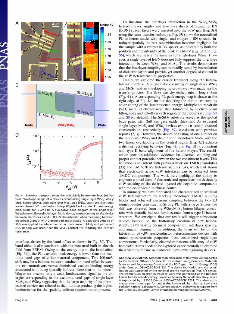
interface, driven by the band offset as shown in Fig. 3C. Thatband offset is also consistent with the measured built-in electricfield from PEEM. Owing to the energy lost to the band offset(Fig. 3C), the PL excitonic peak energy is lower than the exci-tonic band gaps of either material component. This 100-meVshift may be a balance between conduction band offset betweenthe two monolayers versus diminished exciton binding energyassociated with being spatially indirect. Note that in the hetero-bilayer we observe only a weak luminescence signal at the en-ergies corresponding to the excitonic band gaps of single-layerMoS2 and WSe2, suggesting that the large majority of the photo-excited carriers are relaxed at the interface producing the highestluminescence for the spatially indirect recombination process.
To fine-tune the interlayer interaction in the WSe2/MoS2hetero-bilayer, single- and few-layer sheets of hexagonal BN(h-BN) spacer layers were inserted into the vdW gap (Fig. 3D)using the same transfer technique. Fig. 3E shows the normalizedPL of hetero-stacks with single- and trilayer h-BN spacers. In-terlayer spatially indirect recombination becomes negligible forthe sample with a trilayer h-BN spacer, as indicated by both theposition and the intensity of the peak at 1.64 eV (Fig. 3E and Fig.S6), which are nearly the same as for single-layer WSe2. How-ever, a single layer of h-BN does not fully suppress the interlayerinteraction between WSe2 and MoS2. The results demonstratethat the interlayer coupling can be readily tuned by intercalationof dielectric layers and provide yet another degree of control inthe vdW heterostructure properties.Finally, we explored the carrier transport along the hetero-
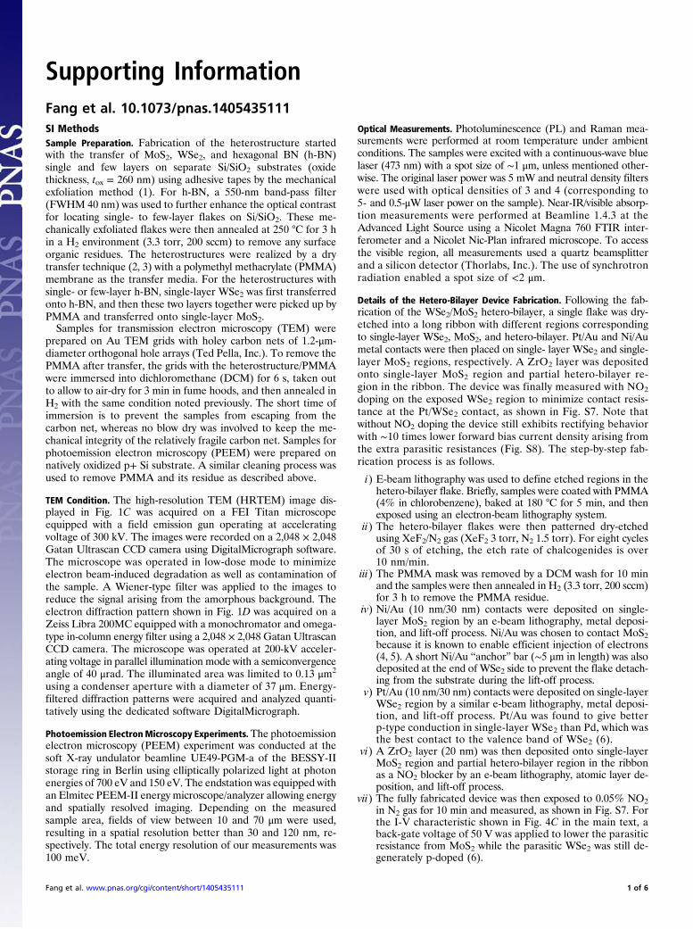
bilayer interface. A single flake consisting of single-layer WSe2and MoS2, and an overlapping hetero-bilayer was made via thetransfer process. The flake was dry etched into a long ribbon(Fig. 4A). A corresponding PL peak energy map is shown at theright edge of Fig. 4A, further depicting the ribbon structure bycolor coding of the luminescence energy. Multiple source/drain(S/D) metal electrodes were then fabricated by electron beamlithography and lift-off on each region of the ribbon (see Figs. S7and S8 for details). The Si/SiO2 substrate serves as the globalback gate, with 260 nm gate oxide thickness. As expectedsingle-layer MoS2 and WSe2 devices exhibit n- and p-channelcharacteristics, respectively (Fig. S9), consistent with previousreports (2, 3). However, the device consisting of one contact onthe monolayer WSe2 and the other on monolayer MoS2, with thetwo layers overlapping in the central region (Fig. 4B) exhibitsa distinct rectifying behavior (Fig. 4C and Fig. S10), consistentwith type II band alignment of the hetero-bilayer. The rectifi-cation provides additional evidence for electrical coupling andproper contact potential between the two constituent layers. Thisbehavior is consistent with previous work on TMDC/nanotubes(33) and TMDC/III-V heterostructures (34), which had shownthat electrically active vdW interfaces can be achieved fromTMDC components. The work here highlights the ability toengineer a novel class of electronic and optoelectronic devices byvdW stacking of the desired layered chalcogenide componentswith molecular-scale thickness control.In summary, we have fabricated and characterized an artificial
vdW heterostructure by stacking monolayer TMDC buildingblocks and achieved electronic coupling between the two 2Dsemiconductor constituents. Strong PL with a large Stokes-likeshift was observed from the WSe2/MoS2 hetero-bilayer, consis-tent with spatially indirect luminescence from a type II hetero-structure. We anticipate that our result will trigger subsequentstudies focused on the bottom-up creation of new hetero-structures by varying chemical composition, interlayer spacing,and angular alignment. In addition, the focus will be on thefabrication of vdW semiconductor heterostructure devices withtuned optoelectronic properties from customized single-layercomponents. Particularly, electroluminescene efficiency of vdWheterostructures needs to be explored experimentally to examinetheir viability for use as nanoscale light-emitting/lasing devices.
ACKNOWLEDGMENTS. Materials characterization of this work was supportedby the director, Office of Science, Office of Basic Energy Sciences, MaterialsSciences and Engineering Division of the US Department of Energy (DOE)under Contract DE-AC02-05CH11231. The device fabrication and character-ization was supported by the National Science Foundation (NSF) E3S center.The transmission electron microscopy work was performed at the NationalCenter for Electron Microscopy, Lawrence Berkeley National Laboratory, whichis supported by US DOE Contract DE-AC02-05CH11231. The absorptionmeasurements were performed at the Advanced Light Source, LawrenceBerkeley National Laboratory. C. Carraro and R.M. acknowledge support fromNSF Grant EEC-0832819 (Center of Integrated Nanomechanical Systems).
A
B
C
4 μm
WSe2/MoS2
Ni/Au
Ni/Au
Pt/A
u
1 2
3456 7
Units: eV
1.85
1.80
1.75
1.70
1.65
1.60
1.55
1
2
3
4
5
WSe2/MoS2Ni/Au Pt/Au
SL MoS2
-6 -3 0 3 6
10-10
10-8
10-6
I 23 (A
)
V23 (V)
Fig. 4. Electrical transport across the WSe2/MoS2 hetero-interface. (A) Op-tical microscope image of a device encompassing single-layer WSe2, WSe2/MoS2 hetero-bilayer, and single-layer MoS2 on a Si/SiO2 substrate. Electrodesare numbered 1–7 from bottom to top. (Right) A color-coded PL peak energymap. (Scale bar, 2 μm.) (B) A qualitative band diagram of the single-layerWSe2/hetero-bilayer/single-layer MoS2 device, corresponding to the devicebetween electrodes 2 and 3. (C) I-V characteristic when measuring betweenelectrodes 2 and 3, with 2 grounded and 3 biased. A back-gate voltage of50 V was applied to reduce the contact resistance to MoS2 and patternedNO2 doping was used near the WSe2 contact for reducing the contactresistance.
Fang et al. PNAS | April 29, 2014 | vol. 111 | no. 17 | 6201
APP
LIED
PHYS
ICAL
SCIENCE
S

1. Mak KF, Lee C, Hone J, Shan J, Heinz TF (2010) Atomically thin MoS2: A new direct-gapsemiconductor. Phys Rev Lett 105(13):136805.
2. Radisavljevic B, Radenovic A, Brivio J, Giacometti V, Kis A (2011) Single-layer MoS2transistors. Nat Nanotechnol 6(3):147–150.
3. Fang H, et al. (2012) High-performance single layered WSe2 p-FETs with chemicallydoped contacts. Nano Lett 12(7):3788–3792.
4. Wang H, et al. (2012) Integrated circuits based on bilayer MoS2 transistors. Nano Lett12(9):4674–4680.
5. Zeng H, Dai J, Yao W, Xiao D, Cui X (2012) Valley polarization in MoS2 monolayers byoptical pumping. Nat Nanotechnol 7(8):490–493.
6. Jones AM, et al. (2013) Optical generation of excitonic valley coherence in monolayerWSe2. Nat Nanotechnol 8(9):634–638.
7. Geim AK, Grigorieva IV (2013) Van der Waals heterostructures. Nature 499(7459):419–425.
8. Yu WJ, et al. (2013) Vertically stacked multi-heterostructures of layered materials forlogic transistors and complementary inverters. Nat Mater 12(3):246–252.
9. Georgiou T, et al. (2013) Vertical field-effect transistor based on graphene-WS2 het-erostructures for flexible and transparent electronics. Nat Nanotechnol 8(2):100–103.
10. Yu WJ, et al. (2013) Highly efficient gate-tunable photocurrent generation in verticalheterostructures of layered materials. Nat Nanotechnol 8(12):952–958.
11. Britnell L, et al. (2013) Strong light-matter interactions in heterostructures of atom-ically thin films. Science 340(6138):1311–1314.
12. Wilson J, Yoffe A (1969) The transition metal dichalcogenides discussion and in-terpretation of the observed optical, electrical and structural properties. Adv Phys18(73):193–335.
13. Terrones H, López-Urías F, Terrones M (2013) Novel hetero-layered materials withtunable direct band gaps by sandwiching different metal disulfides and diselenides.Sci Rep 3:1549.
14. Kang J, Li J, Li S-S, Xia J-B, Wang L-W (2013) Electronic structural Moiré pattern effectson MoS2/MoSe2 2D heterostructures. Nano Lett 13(11):5485–5490.
15. Ko�smider K, Fernández-Rossier J (2013) Electronic properties of the MoS2-WS2 het-erojunction. Phys Rev B 87(7):075451.
16. Komsa H-P, Krasheninnikov AV (2013) Electronic structures and optical properties ofrealistic transition metal dichalcogenide heterostructures from first principles. PhysRev B 88(8):085318.
17. Gong C, et al. (2013) Band alignment of two-dimensional transition metal dichalco-genides: Application in tunnel field effect transistors. Appl Phys Lett 103(5):053513.
18. Dean CR, et al. (2010) Boron nitride substrates for high-quality graphene electronics.
Nat Nanotechnol 5(10):722–726.19. Ponomarenko L, et al. (2011) Tunable metal-insulator transition in double-layer
graphene heterostructures. Nat Phys 7(12):958–961.20. Haigh SJ, et al. (2012) Cross-sectional imaging of individual layers and buried
interfaces of graphene-based heterostructures and superlattices. Nat Mater 11(9):
764–767.21. Britnell L, et al. (2012) Field-effect tunneling transistor based on vertical graphene
heterostructures. Science 335(6071):947–950.22. Gorbachev R, et al. (2012) Strong Coulomb drag and broken symmetry in double-layer
graphene. Nat Phys 8:896–901.23. Hunt B, et al. (2013) Massive Dirac fermions and Hofstadter butterfly in a van der
Waals heterostructure. Science 340(6139):1427–1430.24. Ponomarenko LA, et al. (2013) Cloning of Dirac fermions in graphene superlattices.
Nature 497(7451):594–597.25. Dean CR, et al. (2013) Hofstadter’s butterfly and the fractal quantum Hall effect in
moiré superlattices. Nature 497(7451):598–602.26. Yankowitz M, et al. (2012) Emergence of superlattice Dirac points in graphene on
hexagonal boron nitride. Nat Phys 8(5):382–386.27. Zeng H, et al. (2013) Optical signature of symmetry variations and spin-valley coupling
in atomically thin tungsten dichalcogenides. Sci Rep 3:1608.28. Zhao W, et al. (2013) Evolution of electronic structure in atomically thin sheets of WS2
and WSe2. ACS Nano 7(1):791–797.29. Van Roosbroeck W, Shockley W (1954) Photon-radiative recombination of electrons
and holes in germanium. Phys Rev 94(6):1558.30. Kost A, Lee H, Zou Y, Dapkus P, Garmire E (1989) Band-edge absorption coefficients
from photoluminescence in semiconductor multiple quantum wells. Appl Phys Lett
54(14):1356–1358.31. Wilson BA (1988) Carrier dynamics and recombination mechanisms in staggered-
alignment heterostructures. IEEE J Quantum Electron 24(8):1763–1777.32. Li G, Zhu R, Yang Y (2012) Polymer solar cells. Nat Photonics 6(3):153–161.33. Jariwala D, et al. (2013) Gate-tunable carbon nanotube-MoS2 heterojunction p-n
diode. Proc Natl Acad Sci USA 110(45):18076–18080.34. Chuang S, et al. (2013) Near-ideal electrical properties of InAs/WSe2 van der Waals
heterojunction diodes. Appl Phys Lett 102(24):242101.
6202 | www.pnas.org/cgi/doi/10.1073/pnas.1405435111 Fang et al.
Supporting InformationFang et al. 10.1073/pnas.1405435111SI MethodsSample Preparation. Fabrication of the heterostructure startedwith the transfer of MoS2, WSe2, and hexagonal BN (h-BN)single and few layers on separate Si/SiO2 substrates (oxidethickness, tox = 260 nm) using adhesive tapes by the mechanicalexfoliation method (1). For h-BN, a 550-nm band-pass filter(FWHM 40 nm) was used to further enhance the optical contrastfor locating single- to few-layer flakes on Si/SiO2. These me-chanically exfoliated flakes were then annealed at 250 °C for 3 hin a H2 environment (3.3 torr, 200 sccm) to remove any surfaceorganic residues. The heterostructures were realized by a drytransfer technique (2, 3) with a polymethyl methacrylate (PMMA)membrane as the transfer media. For the heterostructures withsingle- or few-layer h-BN, single-layer WSe2 was first transferredonto h-BN, and then these two layers together were picked up byPMMA and transferred onto single-layer MoS2.Samples for transmission electron microscopy (TEM) were
prepared on Au TEM grids with holey carbon nets of 1.2-μm-diameter orthogonal hole arrays (Ted Pella, Inc.). To remove thePMMA after transfer, the grids with the heterostructure/PMMAwere immersed into dichloromethane (DCM) for 6 s, taken outto allow to air-dry for 3 min in fume hoods, and then annealed inH2 with the same condition noted previously. The short time ofimmersion is to prevent the samples from escaping from thecarbon net, whereas no blow dry was involved to keep the me-chanical integrity of the relatively fragile carbon net. Samples forphotoemission electron microscopy (PEEM) were prepared onnatively oxidized p+ Si substrate. A similar cleaning process wasused to remove PMMA and its residue as described above.
TEM Condition. The high-resolution TEM (HRTEM) image dis-played in Fig. 1C was acquired on a FEI Titan microscopeequipped with a field emission gun operating at acceleratingvoltage of 300 kV. The images were recorded on a 2,048 × 2,048Gatan Ultrascan CCD camera using DigitalMicrograph software.The microscope was operated in low-dose mode to minimizeelectron beam-induced degradation as well as contamination ofthe sample. A Wiener-type filter was applied to the images toreduce the signal arising from the amorphous background. Theelectron diffraction pattern shown in Fig. 1D was acquired on aZeiss Libra 200MC equipped with a monochromator and omega-type in-column energy filter using a 2,048 × 2,048 Gatan UltrascanCCD camera. The microscope was operated at 200-kV acceler-ating voltage in parallel illumination mode with a semiconvergenceangle of 40 μrad. The illuminated area was limited to 0.13 μm2
using a condenser aperture with a diameter of 37 μm. Energy-filtered diffraction patterns were acquired and analyzed quanti-tatively using the dedicated software DigitalMicrograph.
Photoemission ElectronMicroscopy Experiments.The photoemissionelectron microscopy (PEEM) experiment was conducted at thesoft X-ray undulator beamline UE49-PGM-a of the BESSY-IIstorage ring in Berlin using elliptically polarized light at photonenergies of 700 eV and 150 eV. The endstation was equipped withan Elmitec PEEM-II energy microscope/analyzer allowing energyand spatially resolved imaging. Depending on the measuredsample area, fields of view between 10 and 70 μm were used,resulting in a spatial resolution better than 30 and 120 nm, re-spectively. The total energy resolution of our measurements was100 meV.
Optical Measurements. Photoluminescence (PL) and Raman mea-surements were performed at room temperature under ambientconditions. The samples were excited with a continuous-wave bluelaser (473 nm) with a spot size of ∼1 μm, unless mentioned other-wise. The original laser power was 5 mW and neutral density filterswere used with optical densities of 3 and 4 (corresponding to5- and 0.5-μW laser power on the sample). Near-IR/visible absorp-tion measurements were performed at Beamline 1.4.3 at theAdvanced Light Source using a Nicolet Magna 760 FTIR inter-ferometer and a Nicolet Nic-Plan infrared microscope. To accessthe visible region, all measurements used a quartz beamsplitterand a silicon detector (Thorlabs, Inc.). The use of synchrotronradiation enabled a spot size of <2 μm.
Details of the Hetero-Bilayer Device Fabrication. Following the fab-rication of the WSe2/MoS2 hetero-bilayer, a single flake was dry-etched into a long ribbon with different regions correspondingto single-layer WSe2, MoS2, and hetero-bilayer. Pt/Au and Ni/Aumetal contacts were then placed on single- layer WSe2 and single-layer MoS2 regions, respectively. A ZrO2 layer was depositedonto single-layer MoS2 region and partial hetero-bilayer re-gion in the ribbon. The device was finally measured with NO2doping on the exposed WSe2 region to minimize contact resis-tance at the Pt/WSe2 contact, as shown in Fig. S7. Note thatwithout NO2 doping the device still exhibits rectifying behaviorwith ∼10 times lower forward bias current density arising fromthe extra parasitic resistances (Fig. S8). The step-by-step fab-rication process is as follows.
i) E-beam lithography was used to define etched regions in thehetero-bilayer flake. Briefly, samples were coated with PMMA(4% in chlorobenzene), baked at 180 °C for 5 min, and thenexposed using an electron-beam lithography system.
ii) The hetero-bilayer flakes were then patterned dry-etchedusing XeF2/N2 gas (XeF2 3 torr, N2 1.5 torr). For eight cyclesof 30 s of etching, the etch rate of chalcogenides is over10 nm/min.
iii) The PMMA mask was removed by a DCM wash for 10 minand the samples were then annealed in H2 (3.3 torr, 200 sccm)for 3 h to remove the PMMA residue.
iv) Ni/Au (10 nm/30 nm) contacts were deposited on single-layer MoS2 region by an e-beam lithography, metal deposi-tion, and lift-off process. Ni/Au was chosen to contact MoS2because it is known to enable efficient injection of electrons(4, 5). A short Ni/Au “anchor” bar (∼5 μm in length) was alsodeposited at the end of WSe2 side to prevent the flake detach-ing from the substrate during the lift-off process.
v) Pt/Au (10 nm/30 nm) contacts were deposited on single-layerWSe2 region by a similar e-beam lithography, metal deposi-tion, and lift-off process. Pt/Au was found to give betterp-type conduction in single-layer WSe2 than Pd, which wasthe best contact to the valence band of WSe2 (6).
vi) A ZrO2 layer (20 nm) was then deposited onto single-layerMoS2 region and partial hetero-bilayer region in the ribbonas a NO2 blocker by an e-beam lithography, atomic layer de-position, and lift-off process.
vii) The fully fabricated device was then exposed to 0.05% NO2in N2 gas for 10 min and measured, as shown in Fig. S7. Forthe I-V characteristic shown in Fig. 4C in the main text, aback-gate voltage of 50 V was applied to lower the parasiticresistance from MoS2 while the parasitic WSe2 was still de-generately p-doped (6).
Fang et al. www.pnas.org/cgi/content/short/1405435111 1 of 6
TEM AnalysisThe lattice constants of the real lattices can be calculated from
1d2
=43h2 + k2 + hk
a2;
where d is the length of the reciprocal lattice vector of the crystallattice planes of (hk0) and a is the lattice constant of the chal-cogenide crystal. This calculation yields a value of (4.4 ± 0.1)%for the lattice mismatch between the WSe2 single layer and theunderneath MoS2 single layer, which is nearly identical to theirbulk value. The alignment of the two lattices can also be exam-ined with a fast Fourier transform of the two zoomed-in TEMimages in Fig. 1C in the main text, as shown in Fig. S1.
Raman Characterization of the WSe2/MoS2 Hetero-BilayerThere are four Raman-active modes for both WSe2 and MoS2, ofwhich only A1g and E1
2g modes were observed in our measure-ments owing to the selection rule in the back-scattering config-uration and the restricted rejection against Rayleigh scattering(7). As shown in Fig. S2, the in-plane E1
2g mode peaks of WSe2and MoS2 remained unchanged (within 0.5 cm−1) comparingbefore and after transferring. This is a clear indication that thereis no/negligible strain in either layer in the final hetero-bilayer,consistent with our TEM analysis. The out-of-plane A1g modepeak red-shifted by ∼1 cm−1 (from 405.1 cm−1 to 404.1 cm−1) forMoS2, whereas for WSe2 it is hard to detect because the A1gpeak is overlapping with the E1
2g peak. This small red shiftshould be attributed to the interlayer coupling, which is also seenin bulk/few-layer WSe2 and MoS2 (7, 8).
PEEM Experiment DetailAs shown in Fig. S3A, a WSe2/MoS2 hetero-stack, which con-tained a single-layer WSe2 on top of MoS2 with thicknessesranging from one single layer to two single layers and four singlelayers was measured and analyzed by PEEM. Note that thethicknesses of the layers were determined by optical contrast,atomic force microscope in combination with PL. Fig. S3B showsthe W 4f7/2 binding energy position contour, where distinctboundaries between regions can be visualized and are consistentwith our sample geometry. The binding energy map was obtainedby a batch-fitting of all spectra collected at different detectorlocations; single peaks of W 4f7/2 and Mo 3d5/2 were simulatedby a Gaussian profile. For more precise analysis, signals fromhomogeneous parts of the image were spatially integrated andmore sophisticated fitting procedure (a combination of Shirleybackground and Doniach–Sunjic lineshape) was used (Fig. 2). Forthe single-layer WSe2 in contact with the substrate, the W 4f7/2binding energy is 33.78 eV, whereas for the single-layer WSe2 ontop of single-layer MoS2 the W 4f7/2 binding energy is 33.56 eV.The W 4f7/2 core level binding energy decreased by ∼220 meVwhen contacting to MoS2, as noted in the text. The direction ofthe peak shift is consistent with a negative net charge on theWSe2 in the WSe2/MoS2 hetero-bilayer, as predicted by densityfunctional theory (9). However, charge neutrality in the hetero-bilayer requires that a shift in the opposite direction be presenton the MoS2 component of WSe2/MoS2. As is shown in Fig.S3C, a shift of +190 meV with respect to stand-alone MoS2 isindeed observed in the Mo 3d core levels of the WSe2/MoS2(from 227.26 eV to 227.45 eV). The shifts in the W and Mo corelevels are evidence that there exists a charge transfer-inducedelectric field between WSe2 and MoS2 layers. The hetero-bilayer
can essentially be interpreted as being a 2D dipole, an atomicallythin parallel plate capacitor with van der Waals gap. One canalso notice that the W 4f7/2 binding energy position shifted lesswhen contacting to thicker MoS2 layers by ∼30 meV per layer. Itis not clear at this stage which one of the three parameters,namely, the charge-transfer amount, layer distance, or the di-electric constant in the van der Waals gap, is playing a moreimportant role in this slight decrease. Detailed density func-tional theory calculations are needed to further shed light onthis issue.
Luminescence Tail AnalysisThe band edge tail D(ν) as a function of frequency ν [also calledthe Urbach tail (10)], is related to the photon emission rate perunit energy by the van Roosbroeck–Shockley equation (11, 12).D(ν) can further be related to the photoluminescence spectrum I(ν) by
DðνÞ∝ IðνÞ�ehν=kT − 1�
n2r ν2;
where h is Planck’s constant, k is Boltzmann’s constant, T istemperature, and nr is the real part of the refractive index. Fig.S5 shows the shapes of the Urbach tails of single-layer WSe2,single-layer MoS2, and the WSe2/MoS2 hetero-bilayer. An opti-cal semilog inverse slope of 30 meV/dec is extracted from allthree tails, corresponding to the sharpness of the band edge.The nearly identical inverse slope of the hetero-bilayer provesthat the band edge sharpness of the heterostructure can be ashigh as that of its constituent single layers.
Absolute PL Spectra of WSe2/MoS2 Heterostructure withh-BNFig. S6 shows the absolute PL of WSe2/MoS2 hetero-stacks withsingle- and trilayer h-BN spacers, along with the PL of single-layer WSe2. Interlayer coupling becomes negligible for thesample with a trilayer h-BN spacer, as indicated by both theposition and the intensity of the peak at 1.64 eV, which arenearly the same as single-layer WSe2. The slight difference (0.01eV) in the peak position is likely due to the fact that theboundary on the bottom side of WSe2 has changed from SiO2 toh-BN. On the other band, a single layer of h-BN does not fullysuppress the interlayer interaction between WSe2 and MoS2. ThePL spectrum of WSe2/h-BN/MoS2 shows a double peak featurecentered at 1.6 eV with an intensity on the order of one-third ofthat of typical single-layer WSe2. We interpret the lower energypeak component of the doublet as being the peak of the hetero-bilayer with reduced interlayer coupling owing to the in-tercalation of the h-BN single layer. Indeed, this peak falls inbetween the peak of the unperturbed single-layer WSe2 andstrongly coupled WSe2/MoS2 bilayer. This demonstrates that theinterlayer coupling can be readily tuned by intercalation of lay-ered dielectric media into the van der Waals gap. The higherenergy peak closely coincides with the peak of single-layer WSe2and could be due to a competing spatially direct emission insingle-layer WSe2 as the photo-generated electrons now see aBN barrier and would have certain probability of staying in theexcitonic conduction band edge of WSe2. This interpretation isalso supported by the weak emission close to the position ofsingle-layer MoS2.
1. Novoselov KS, et al. (2004) Electric field effect in atomically thin carbon films. Science306(5696):666–669.
2. Dean CR, et al. (2010) Boron nitride substrates for high-quality graphene electronics.Nat Nanotechnol 5(10):722–726.
3. Ponomarenko L, et al. (2011) Tunable metal-insulator transition in double-layer grapheneheterostructures. Nat Phys 7(12):958–961.
4. Fang H, et al. (2013) Degenerate n-doping of few-layer transition metal dichalcogenidesby potassium. Nano Lett 13(5):1991–1995.
Fang et al. www.pnas.org/cgi/content/short/1405435111 2 of 6
5. Liu H, Neal AT, Ye PD (2012) Channel length scaling of MoS2 MOSFETs. ACS Nano6(10):8563–8569.
6. Fang H, et al. (2012) High-performance single layered WSe2 p-FETs with chemicallydoped contacts. Nano Lett 12(7):3788–3792.
7. Zeng H, et al. (2013) Optical signature of symmetry variations and spin-valley couplingin atomically thin tungsten dichalcogenides. Sci Rep 3:1608.
8. Lee C, et al. (2010) Anomalous lattice vibrations of single- and few-layer MoS2. ACSNano 4(5):2695–2700.
9. Terrones H, López-Urías F, Terrones M (2013) Novel hetero-layered materials with tunabledirect band gaps by sandwiching different metal disulfides and diselenides. Sci Rep 3:1549.
10. Urbach F (1953) The long-wavelength edge of photographic sensitivity and of theelectronic absorption of solids. Phys Rev 92:1324.
11. Van Roosbroeck W, Shockley W (1954) Photon-radiative recombination of electronsand holes in germanium. Phys Rev 94(6):1558.
12. Kost A, Lee H, Zou Y, Dapkus P, Garmire E (1989) Band-edge absorption coefficientsfrom photoluminescence in semiconductor multiple quantum wells. Appl Phys Lett54(14):1356–1358.
A
B
12.5°
WSe2-MoS2 hetero-bilayer
SL MoS2
FFT
FFT
Fig. S1. Fast Fourier transform of the HRTEM images shown in Fig. 1C in the main text for (A) WSe2/MoS2 hetero-bilayer and (B) single-layer MoS2.
250 300 350 400
).u.a(ytisnetnI
Raman Shift (cm-1)
SL MoS2
SL WSe2
WSe2-MoS2
A1g A1gE1
2gE1
2g
Fig. S2. Raman spectra comparison for single-layer MoS2 and WSe2 and the WSe2/MoS2 hetero-bilayer. The excitation laser wavelength here is 532 nm.
Fang et al. www.pnas.org/cgi/content/short/1405435111 3 of 6
SL WSe2
MoS2
1L2L
4L
30.8
31.0
31.2
31.4
31.6
31.8
32.0
Binding Energy (eV)
W 4f7/2A B Binding Energy (eV)
226.8
227.0
227.2
227.4
227.6
227.8
C Mo 3d5/2
Fig. S3. (A) The optical microscope image of the WSe2/MoS2 heterostructure for PEEM characterization. The PEEM sample was on a naturally (native) oxidizedheavily p-doped Si substrate, and the image was taken when the sample was on Si/SiO2 (260 nm) substrate. (B) W 4f7/2 binding energy position contour plot ofthe sample in A. (C) Mo 3d5/2 binding energy position contour plot of the sample in A. (Scale bars, 2 μm.)
A B
C
1.4 1.5 1.6 1.7
0
200
400
600 #1 #2 #3 #4 #5 #6 #7 #8 #9 #10
).u.a(stnuoc
LP
Photon energy (eV)
1.50 1.55 1.600
2
4rebmu
N
Peak energy (eV)
0 140 280 420 5600
1
2
3
re bmu
N
Peak intensity (a.u.)
Fig. S4. PL statistics of multiple WSe2/MoS2 hetero-bilayer samples. (A) PL spectra of 10 WSe2/MoS2 hetero-bilayers. (B) Histogram of the PL peak energies forthese 10 samples. (C) Histogram of the PL peak intensities for these 10 samples.
1.4 1.6 1.8
102
103
104
105
106
I()*
(px e
(hkT
)-1) /
2
Photon energy (eV)
Fig. S5. Band edge tails derived from the PL using the van Roosbroeck–Shockley equation, depicting the sharpness of the band edges. The spectra werenormalized to peak magnitude.
Fang et al. www.pnas.org/cgi/content/short/1405435111 4 of 6
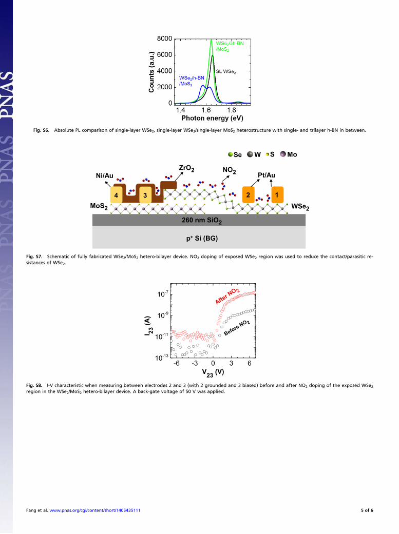
Fig. S6. Absolute PL comparison of single-layer WSe2, single-layer WSe2/single-layer MoS2 heterostructure with single- and trilayer h-BN in between.
NO2
WSe2MoS2
Pt/AuNi/AuZrO2
260 nm SiO2
p+ Si (BG)
1234
WSe S Mo
Fig. S7. Schematic of fully fabricated WSe2/MoS2 hetero-bilayer device. NO2 doping of exposed WSe2 region was used to reduce the contact/parasitic re-sistances of WSe2.
-6 -3 0 3 610-13
10-11
10-9
10-7
I 23)
A(
V (V)
Fig. S8. I-V characteristic when measuring between electrodes 2 and 3 (with 2 grounded and 3 biased) before and after NO2 doping of the exposed WSe2region in the WSe2/MoS2 hetero-bilayer device. A back-gate voltage of 50 V was applied.
Fang et al. www.pnas.org/cgi/content/short/1405435111 5 of 6
-100 -50 0 50 1001E-12
1E-10
1E-8
1E-6
1E-4
I 3 4)
A(
VGS (V)
-100 -50 0 50 1001E-12
1E-10
1E-8
1E-6
1E-4
-I12
)A(
VGS (V)-4 -2 0 2 4
-40
-20
0
20
40
I 21(
A)
V21 (V)
Vgs= 0VVgs= -20VVgs= -40VVgs= -60VVgs= -80VVgs= -100V
V43 = 3 V
V21 = -3 V
-4 -2 0 2 4
-2
0
2
I 43(
A)
V43 (V)
Vgs= 100VVgs= 80VVgs= 60VVgs= 40VVgs= 20VVgs= 0V
A B
C D
Fig. S9. (A) Transfer characteristic of the single-layer WSe2 device in Fig. 4A of the main text (measured between terminals 1 and 2). (B) Output characteristicof the device in A. (C) Transfer characteristic of the single-layer MoS2 device in Fig. 4A of the main text (measured between terminals 3 and 4). (D) Outputcharacteristic of the device in C.
-6 -3 0 3 6
10-10
10-8
10-6
I 23)
A(
V23 (V)
VGS= 100V VGS= 50V VGS= 0V VGS= -50V VGS= -100V
Fig. S10. Gate dependence in the I-V characteristic of WSe2/MoS2 heterojunction. Owing to the parasitic resistances in the WSe2 and MoS2 single layers, the I-Vshows an “anti-ambiploar” behavior, namely, the peak conductance at the forward bias region appears near an intermediate gate bias, which is similar towhat has been previously observed in the MoS2/nanotubes heterostructure (1).
1. Jariwala D, et al. (2013) Gate-tunable carbon nanotube-MoS2 heterojunction p-n diode. Proc Natl Acad Sci USA 110(45):18076–18080.
Fang et al. www.pnas.org/cgi/content/short/1405435111 6 of 6
 where the chara.cterist.ic l.emperal.ure is defined as To = hvpI'lirksTj](https://img.pdfslide.us/doc/110x75/5f1e95597fc47d277e3758b2/interlayer-coupling-in-metallic-magnetic-as-tt0att0-where-the-characteristic.jpg)


![Electronic structure, spin-orbit coupling, and interlayer ...jeng/paper/15/PhysRevB.91.235202.pdf · Electronic structure, spin-orbit coupling, ... as implemented in the VASP [20–22]](https://img.pdfslide.us/doc/110x75/5aed88447f8b9a6625901154/electronic-structure-spin-orbit-coupling-and-interlayer-jengpaper15physrevb91.jpg)