Embed Size (px)
Citation preview
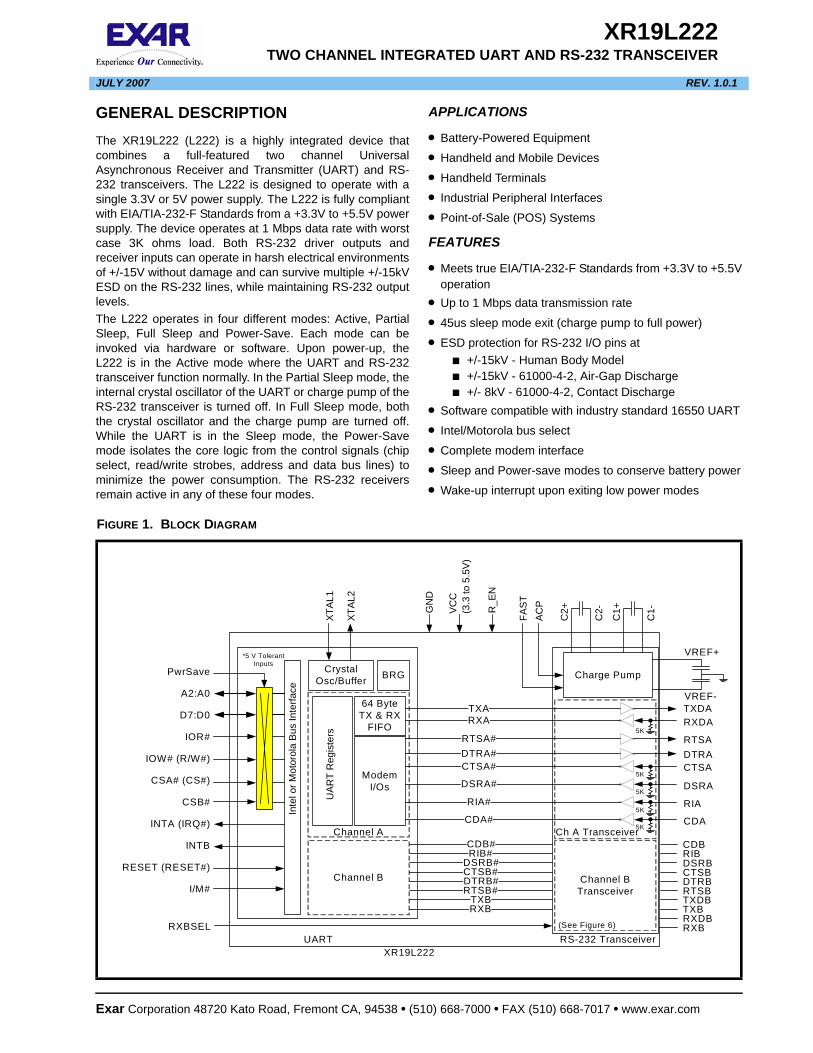
XR19L222TWO CHANNEL INTEGRATED UART AND RS-232 TRANSCEIVER
JULY 2007 REV. 1.0.1
GENERAL DESCRIPTIONThe XR19L222 (L222) is a highly integrated device that combines a full-featured two channel Universal Asynchronous Receiver and Transmitter (UART) and RS-232 transceivers. The L222 is designed to operate with a single 3.3V or 5V power supply. The L222 is fully compliant with EIA/TIA-232-F Standards from a +3.3V to +5.5V power supply. The device operates at 1 Mbps data rate with worst case 3K ohms load. Both RS-232 driver outputs and receiver inputs can operate in harsh electrical environments of +/-15V without damage and can survive multiple +/-15kV ESD on the RS-232 lines, while maintaining RS-232 output levels. The L222 operates in four different modes: Active, Partial Sleep, Full Sleep and Power-Save. Each mode can be invoked via hardware or software. Upon power-up, the L222 is in the Active mode where the UART and RS-232 transceiver function normally. In the Partial Sleep mode, the internal crystal oscillator of the UART or charge pump of the RS-232 transceiver is turned off. In Full Sleep mode, both the crystal oscillator and the charge pump are turned off. While the UART is in the Sleep mode, the Power-Save mode isolates the core logic from the control signals (chip select, read/write strobes, address and data bus lines) to minimize the power consumption. The RS-232 receivers remain active in any of these four modes.
Exar Corporation 48720 Kato Road, Fremont CA, 94538 • (5
APPLICATIONS
• Battery-Powered Equipment
• Handheld and Mobile Devices
• Handheld Terminals
• Industrial Peripheral Interfaces
• Point-of-Sale (POS) Systems
FEATURES
• Meets true EIA/TIA-232-F Standards from +3.3V to +5.5V operation
• Up to 1 Mbps data transmission rate
• 45us sleep mode exit (charge pump to full power)
• ESD protection for RS-232 I/O pins at■ +/-15kV - Human Body Model■ +/-15kV - 61000-4-2, Air-Gap Discharge■ +/- 8kV - 61000-4-2, Contact Discharge
• Software compatible with industry standard 16550 UART
• Intel/Motorola bus select
• Complete modem interface
• Sleep and Power-save modes to conserve battery power
• Wake-up interrupt upon exiting low power modes
FIGURE 1. BLOCK DIAGRAM
XR19L222UART RS-232 Transceiver
Inte
l or M
otor
ola
Bus
Inte
rface
PwrSave
A2:A0
D7:D0
IOR#
IOW# (R/W#)
CSA# (CS#)
CSB#
INTA (IRQ#)
INTB
RESET (RESET#)
I/M#
Crystal Osc/Buffer
XTA
L1
XTA
L2
BRG
64 Byte TX & RX
FIFO
Modem I/Os
UA
RT
Reg
iste
rs
TXARXA
RTSA#DTRA#CTSA#
DSRA#
RIA#
CDA#
Charge Pump
TXDA
RTSADTRA
5KRXDA
5KCTSA
5KDSRA
5KRIA
5KCDA
AC
P
C2+
C2-
C1+
C1-VC
C(3
.3 to
5.5
V)
*5 V Tolerant Inputs
VREF+
VREF-
GN
D
FAS
T
R_E
N
Channel B
CDB#RIB#
DSRB#CTSB#
Channel A
DTRB#RTSB#
TXBRXB
Channel BTransceiver
Ch A Transceiver
RXBSEL
CDBRIBDSRBCTSBDTRBRTSBTXDBTXBRXDBRXB(See Figure 6)
10) 668-7000 • FAX (510) 668-7017 • www.exar.com
XR19L222 TWO CHANNEL INTEGRATED UART AND RS-232 TRANSCEIVER REV. 1.0.1
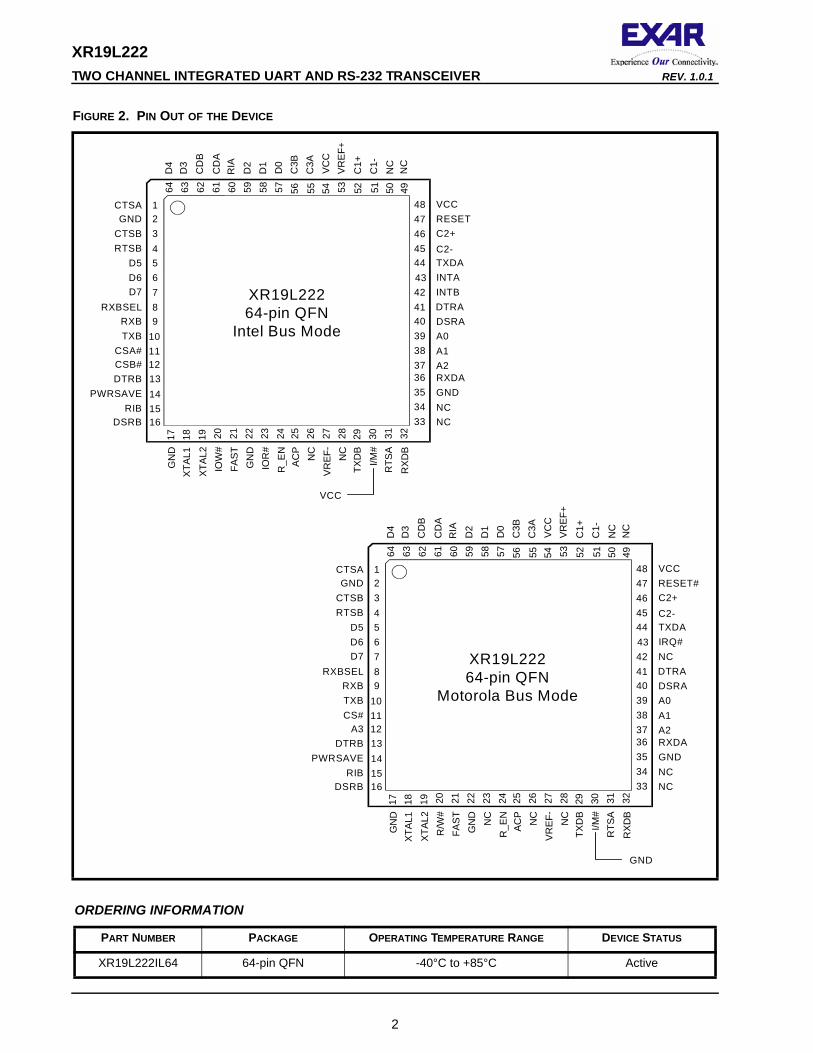
FIGURE 2. PIN OUT OF THE DEVICE
ORDERING INFORMATION
PART NUMBER PACKAGE OPERATING TEMPERATURE RANGE DEVICE STATUS
XR19L222IL64 64-pin QFN -40°C to +85°C Active
64 63 62 61 60 59 58 57 56 55 54 53
123456789
101112
484746454443424140393837
29 30 31 3217 18 19 20 21 22 23 24
CTSAGND
CTSBRTSB
D5D6D7
RXBSEL
TXBRXB
CSA#CSB#
TXD
BI/M
#R
TSA
RX
DB
GN
DX
TAL1
XTA
L2IO
W#
FAST
GN
DIO
R#
R_E
N
VCCRESETC2+C2-TXDAINTAINTBDTRADSRAA0A1A2
D4
D3
D2
D1
D0
C3B
C3A
VCC
VR
EF+
XR19L22264-pin QFN
Intel Bus Mode
13141516
PWRSAVEDTRB
RIBDSRB
25 26 27 28
AC
PN
CV
REF
-N
C
36353433
RXDAGNDNCNC
52 51 50 49
C1+
C1-
NC
NC
RIA
CD
A
CD
B
VCC
64 63 62 61 60 59 58 57 56 55 54 53123456789
101112
484746454443424140393837
29 30 31 3217 18 19 20 21 22 23 24
CTSAGND
CTSBRTSB
D5D6D7
RXBSEL
TXBRXB
CS#A3
TXD
BI/M
#R
TSA
RX
DB
GN
DX
TAL1
XTA
L2R
/W#
FAS
TG
ND
NC
R_E
N
VCCRESET#C2+C2-TXDAIRQ#NCDTRADSRAA0A1A2
D4
D3
D2
D1
D0
C3B
C3A
VC
CV
RE
F+
XR19L22264-pin QFN
Motorola Bus Mode
13141516
PWRSAVEDTRB
RIBDSRB
25 26 27 28
AC
PN
CV
RE
F- NC
36353433
RXDAGNDNCNC
52 51 50 49
C1+
C1-
NC
NC
RIA
CD
A
CD
B
GND
2
XR19L222REV. 1.0.1 TWO CHANNEL INTEGRATED UART AND RS-232 TRANSCEIVER
PIN DESCRIPTIONS Pin Descriptions
NAME64-QFN
PIN# TYPE DESCRIPTION
DATA BUS INTERFACE (CMOS/TTL Voltage Levels)
A2A1A0
373839
I Address bus lines [2:0]. These 3 address lines select one of the internal registers in the UART during a data bus transaction.
D7D6D5D4D3D2D1D0
765
6463595857
I/O Data bus lines [7:0] (bidirectional).
IOR#(NC)
23 I When I/M# pin is HIGH, the Intel bus interface is selected and this input becomes read strobe (active LOW). The falling edge instigates an internal read cycle and retrieves the data byte from an internal register pointed by the address lines [A2:A0], puts the data byte on the data bus to allow the host processor to read it on the rising edge.When I/M# pin is LOW, the Motorola bus interface is selected and this input is not used.
IOW#(R/W#)
20 I When I/M# pin is HIGH, it selects Intel bus interface and this input becomes write strobe (active LOW). The falling edge instigates the internal write cycle and the rising edge trans-fers the data byte on the data bus to an internal register pointed by the address lines.When I/M# pin is LOW, the Motorola bus interface is selected and this input becomes read (HIGH) and write (LOW) signal.
CSA#(CS#)
11 I When I/M# pin is HIGH, this input is chip select A (active low) to enable channel A in the device.When I/M# pin is LOW, this input becomes the chip select (active low) for the Motorola bus interface.
CSB#(A3)
12 I When I/M# pin is HIGH, this input is chip select B (active low) to enable channel B in the device.When I/M# pin is LOW, this input becomes address line A3 which is used for channel selec-tion in the Motorola bus interface. Input logic 0 selects channel A and logic 1 selects chan-nel B.
INTA(IRQ#)
43 O(OD)
When I/M# pin is HIGH, it selects Intel bus interface and this output become the active HIGH device interrupt output for channel A. This output is enabled through the software set-ting of MCR[3]: set to the active mode when MCR[3] is set to a logic 1, and set to the three state mode when MCR[3] is set to a logic 0. See MCR[3]. When I/M# pin is LOW, it selects Motorola bus interface and this output becomes the active LOW, open-drain interrupt output for both channels. An external pull-up resistor is required for proper operation. MCR[3] must be set to a logic 0 for proper operation of the interrupt.
INTB(NC)
42 O(OD)
When I/M# pin is HIGH, it selects Intel bus interface and this output become the active HIGH device interrupt output for channel B. This output is enabled through the software set-ting of MCR[3]: set to the active mode when MCR[3] is set to a logic 1, and set to the three state mode when MCR[3] is set to a logic 0. See MCR[3]. When I/M# pin is LOW, it selects Motorola bus interface and this output is not used and can be left unconnected.
3
XR19L222 TWO CHANNEL INTEGRATED UART AND RS-232 TRANSCEIVER REV. 1.0.1
MODEM OR SERIAL I/O INTERFACE (EIA-232/RS-232 Voltage Levels)
TXDA 44 O UART Channel A Transmit Data. The TX signal will be LOW (< 1.5V) during reset or idle (no data).
RXDA 36 I UART Channel A Receive Data. The RX data input must idle LOW (< 1.5V). This input has an internal pull-down resistor and can be left unconnected when not used.
RTSA 31 O UART Channel A Request-to-Send or general purpose outputs. These outputs must be asserted prior to using auto RTS flow control, see EFR[6], MCR[1] and IER[6].
CTSA 1 I UART Channel A Clear-to-Send or general purpose inputs. It can be used for auto CTS flow control, see EFR[7], MSR[4] and IER[7]. This input has an internal pull-down resistor and can be left unconnected when not used.
DTRA 41 O UART Channel A Data-Terminal-Ready or general purpose outputs.
DSRA 40 I UART Channel A Data-Set-Ready or general purpose inputs. This input has an internal pull-down resistor and can be left unconnected when not used.
CDA 61 I UART Channel A Carrier-Detect or general purpose inputs. This input has an internal pull-down resistor and can be left unconnected when not used.
RIA 60 I UART Channel A Ring-Indicator or general purpose inputs. This input has an internal pull-down resistor and can be left unconnected when not used.
TXDB 29 O UART Channel B Transmit Data. The TX signal will be LOW (< 1.5V) during reset or idle (no data).
RXDB 32 I UART Channel B Receive Data. RXDB will be the input signal to the internal UART when RXBSEL is LOW. If RXB is used, then RXBSEL should be HIGH. The RX data input must idle LOW (< 1.5V). This input has an internal pull-down resistor and can be left uncon-nected when not used.
RTSB 4 O UART Channel B Request-to-Send or general purpose outputs. These outputs must be asserted prior to using auto RTS flow control, see EFR[6], MCR[1] and IER[6].
CTSB 3 I UARTChannel B Clear-to-Send or general purpose inputs. It can be used for auto CTS flow control, see EFR[7], MSR[4] and IER[7]. This input has an internal pull-down resistor and can be left unconnected when not used.
DTRB 13 O UART Channel B Data-Terminal-Ready or general purpose outputs.
DSRB 16 I UART Channel B Data-Set-Ready or general purpose inputs. This input has an internal pull-down resistor and can be left unconnected when not used.
CDB 62 I UART Channel B Carrier-Detect or general purpose inputs. This input has an internal pull-down resistor and can be left unconnected when not used.
RIB 15 I UART Channel B Ring-Indicator or general purpose inputs. This input has an internal pull-down resistor and can be left unconnected when not used.
SERIAL I/O INTERFACE (CMOS/TTL Voltage Levels)
TXB 10 O UART Channel B Transmit data. This is the TXB output signal from the UART. This pin can be used to communicate with an external Infrared or RS-422 transceiver if TXDB is unused.
RXB 9 I UART Channel B Receive data. This is the RXB input signal to the UART. If RXDB is not used (RXBSEL is HIGH), then this pin can be used to communicate with an external Infra-red or RS-422 transceiver. If RXDB is used (RXBSEL is LOW), this pin should be left open.
Pin Descriptions
NAME64-QFN
PIN# TYPE DESCRIPTION
4
XR19L222REV. 1.0.1 TWO CHANNEL INTEGRATED UART AND RS-232 TRANSCEIVER
ANCILLARY SIGNALS (CMOS/TTL Voltage Levels)
XTAL1 18 I Crystal or external clock input. This input is not 5V tolerant.
XTAL2 19 O Crystal or buffered clock output. This output may be use to drive a clock buffer which can drive other device(s).
PwrSave 14 I Power-Save (active high). This feature isolates the L222’s data bus interface from the host preventing other bus activities that cause higher power drain during sleep mode. See Sleep Mode with Auto Wake-up and Power-Save Feature section for details.
ACP 25 I Autosleep for Charge Pump (active HIGH). When this pin is HIGH, the charge pump is shut off if the L222 is already in partial sleep mode, i.e. the crystal oscillator is stopped. See ”Section 2.18, Sleep Modes and Power-Save Feature with Wake-Up Inter-rupt” on page 20.
I/M# 30 I Intel or Motorola Bus Select. When I/M# pin is HIGH, 16 or Intel Mode, the device will operate in the Intel bus type of interface.When I/M# pin is LOW, 68 or Motorola mode, the device will operate in the Motorola bus type of interface.
RESET(RESET#)
47 I When I/M# pin is HIGH for Intel bus interface, this input becomes RESET (active high). When I/M# pin is LOW for Motorola bus interface, this input becomes RESET# (active low). A 40 ns minimum active pulse on this pin will reset the internal registers and all outputs of the UART. The UART transmitter output will be held HIGH, the receiver input will be ignored and outputs are reset during reset period (see Table 16).
C2+C2-
4645
- Charge pump capacitors. As shown in Figure 1, a 0.1 uF capacitor should be placed between these 2 pins.
C1+C1-
5251
- Charge pump capacitors. As shown in Figure 1, a 0.1 uF capacitor should be placed between these 2 pins.
VREF+ 53 Pwr +5.0V generated by the charge pump.
VREF- 27 Pwr -5.0V generated by the charge pump.
R_EN 24 I When the supply voltage is < 3.6V, connect R_EN to VCC.When the supply voltage is > 3.6V, connect R_EN to GND.
C3AC3B
5556
I When the supply voltage is 3.3 V, C3A and C3B should be connected to VCC.When the supply voltage is 5 V, C3A should be connected to C3B with a 1 uF capacitor to GND.
RXBSEL 8 I When RXBSEL is HIGH, RXB is the input to the receiver of the UART.When RXBSEL is LOW, RXDB is the input to the receiver of the UART.
FAST 21 I When FAST is HIGH, the maximum serial data rate is 1 Mbps.When FAST is LOW, the maximum serial data rate is 250 Kbps.
VCC 48, 54 Pwr 3.3V to 5.5V power supply. All CMOS/TTL input pins, except XTAL1, are 5V tolerant.
GND 2, 17, 22, 35
Pwr Power supply common, ground.
Pin Descriptions
NAME64-QFN
PIN# TYPE DESCRIPTION
5
XR19L222 TWO CHANNEL INTEGRATED UART AND RS-232 TRANSCEIVER REV. 1.0.1
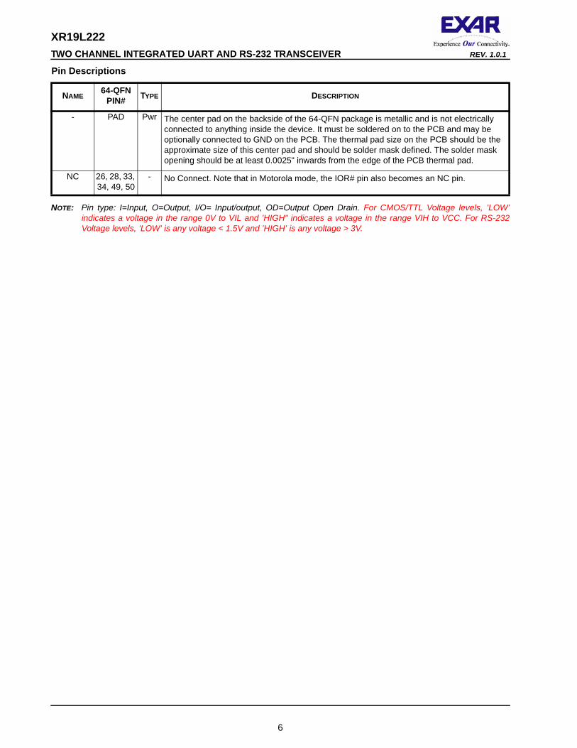
NOTE: Pin type: I=Input, O=Output, I/O= Input/output, OD=Output Open Drain. For CMOS/TTL Voltage levels, ’LOW’ indicates a voltage in the range 0V to VIL and ’HIGH" indicates a voltage in the range VIH to VCC. For RS-232 Voltage levels, ’LOW’ is any voltage < 1.5V and ’HIGH’ is any voltage > 3V.
- PAD Pwr The center pad on the backside of the 64-QFN package is metallic and is not electrically connected to anything inside the device. It must be soldered on to the PCB and may be optionally connected to GND on the PCB. The thermal pad size on the PCB should be the approximate size of this center pad and should be solder mask defined. The solder mask opening should be at least 0.0025" inwards from the edge of the PCB thermal pad.
NC 26, 28, 33, 34, 49, 50
- No Connect. Note that in Motorola mode, the IOR# pin also becomes an NC pin.
Pin Descriptions
NAME64-QFN
PIN# TYPE DESCRIPTION
6
XR19L222REV. 1.0.1 TWO CHANNEL INTEGRATED UART AND RS-232 TRANSCEIVER
1.0 PRODUCT DESCRIPTION The XR19L222 consists of a two-channel UART and RS-232 transceivers. It operates from a single +3V to 5.5V supply with data rates up to 1Mbps, while meeting all EIA RS-232F specifications. Its feature set is fully compatible to the industry standard 16C550. Unlike the 16C550, most of the modem signals are not CMOS/TTL level, but conform to EIA/TIA 232 or RS-232 voltage levels. The only two signals that are CMOS/TTL level are the TXB and RXB signals. They can be used with an external IR or RS-422 transceiver when their corresponding RS-232 signals, TXDB and RXDB, are not used. The configuration register set is 16550 UART compatible for control, status and data transfer. Also, the L222 has 64-bytes of transmit and receive FIFOs, automatic RTS/CTS hardware flow control, automatic Xon/Xoff and special character software flow control, transmit and receive FIFO trigger levels, and a programmable fractional baud rate generator with a prescaler of divide by 1 or 4. Additionally, the L222 includes the ACP pin which the user can shut down the charge pump for the RS-232 drivers. In the UART portion, the Power-Save feature isolates the databus interface to further reduce power consumption in the Sleep mode. The L222 is fabricated using an advanced CMOS process. Enhanced FeaturesThe L222 UART provides a solution that supports 64 bytes of transmit and receive FIFO. Increased performance is realized in the L222 by the transmit and receive FIFOs, FIFO trigger level controls and automatic flow control mechanism. This allows the external processor to handle more networking tasks within a given time. This increases the service interval giving the external CPU additional time for other applications and reducing the overall UART interrupt servicing time. In addition, the L222 provides the ACP and Power-Save modes that drastically reduces the power consumption when the device is not used. The combination of the above greatly reduces the CPU’s bandwidth requirement, increases performance, and reduces power consumption. Intel or Motorola Data Bus InterfaceThe L222 provides a host interface that supports Intel or Motorola microprocessor (CPU) data bus interface. The Intel bus compatible interface allows direct interconnect to Intel compatible type of CPUs using IOR#, IOW# and CS# inputs for data bus operation. The Motorola bus compatible interface instead uses the R/W# and CS# signals for data bus transactions. See pin description section for details on all the control signals. The Intel and Motorola bus interface selection is made through the pin, I/M#. Data RateThe L222 is capable of operation up to 1 Mbps data rate. The UART section can operate at much higher speeds, but the speed of the RS-232 transceiver is limited to 1 Mbps. The device can operate either with a crystal on pins XTAL1 and XTAL2, or external clock source on XTAL1 pin. Internal Enhanced Register SetsThe L222 UART has a set of enhanced registers providing control and monitoring functions. Interrupt enable/disable and status, FIFO enable/disable, selectable TX and RX FIFO trigger levels, automatic hardware/software flow control enable/disable, programmable baud rates, modem interface controls and status, sleep mode and infrared mode are all standard features. Following a power on reset or an external reset (and operating in 16 or Intel Mode), the registers defaults to the reset condition and is compatible with the 16C550.RS-232 InterfaceThe L222 includes RS-232 drivers/receivers for the entire modem interface. This feature eliminates the need for an external RS-232 transceiver. The charge pump provides output voltages of +5V and -5V for its drivers over the 3.3V to 5.5V VCC supply voltage. The serial outputs TXD, RTS and DTR swing between -5V (inactive) and 5V (active) RS-232 voltage levels. The serial inputs RXD, CTS, DSR, CD and RI are RS-232 receivers and can take any voltage swing from -15V to +15V. The receivers are always active, even in Full Sleep and Power-Save modes. The RS-232 drivers guarantee a data rate of 1 Mbps even when fully loaded with 3Kohm in parallel with 1000pF load. All RS-232 drivers and receivers are protected to ±15kV using the Human Body Model ground combination, ±8kV using IEC 61000-4-2 Contact Discharge, and ±15kV using IEC 61000-4-2 Air-Gap Discharge. For more information, send an e-mail to [email protected].
7
XR19L222 TWO CHANNEL INTEGRATED UART AND RS-232 TRANSCEIVER REV. 1.0.1
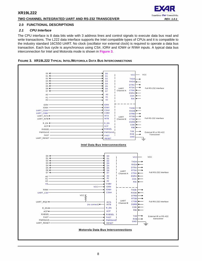
2.0 FUNCTIONAL DESCRIPTIONS2.1 CPU Interface
The CPU interface is 8 data bits wide with 3 address lines and control signals to execute data bus read and write transactions. The L222 data interface supports the Intel compatible types of CPUs and it is compatible to the industry standard 16C550 UART. No clock (oscillator nor external clock) is required to operate a data bus transaction. Each bus cycle is asynchronous using CS#, IOR# and IOW# or R/W# inputs. A typical data bus interconnection for Intel and Motorola mode is shown in Figure 3.
FIGURE 3. XR19L222 TYPICAL INTEL/MOTOROLA DATA BUS INTERCONNECTIONS
VCCVCC
DSRACTSARTSADTRA
RXDATXDA
RIACDA
RXB
DSRBCTSBRTSBDTRBRXDBTXDB
RIBCDB
GND
UARTChannel A
UARTChannel B Full RS-232 Interface
Intel Data Bus Interconnections
TXB
Full RS-232 Interface
D0D1D2D3D4D5D6D7
D0D1D2D3D4D5D6D7
A0A1A2
A0A1A2
UART_CSA#UART_CSB#
IOR#IOW#
CSA#CSB#
IOR#IOW#
UART_INTBUART_INTA
INTBINTA
ACPR_EN
RESET
R_EN
PWRSAVE
ACP
RXBSEL RXBSEL
FASTUART_RESET
PWRSAVE
FAST
External IR or RS-422 Transceiver
VCCVCC
RXB
DSRACTSARTSADTRARXDATXDA
RIACDA
TXB
DSRBCTSBRTSBDTRBRXDBTXDB
RIBCDB
GND
UARTChannel A
UARTChannel B
Full RS-232 Interface
Full RS-232 Interface
Motorola Data Bus Interconnections
UART_IRQ# INTA
VCC
INTB(no connect)
R_EN R_EN
ACP ACP
RXBSELRXBSELFASTFASTPWRSAVEPWRSAVERESETUART_RESET
External IR or RS-422 transceiver
D0D1D2D3D4D5D6D7
D0D1D2D3D4D5D6D7
A0 A0A1 A1A2 A2
IOR#VCCR/W# IOW#
UART_CS# CSA#
A3 CSB#
8
XR19L222REV. 1.0.1 TWO CHANNEL INTEGRATED UART AND RS-232 TRANSCEIVER
2.2 5-Volt Tolerant InputsThe CMOS/TTL level inputs of the L222 can accept up to 5V inputs when operating at 3.3V. Note that the XTAL1 pin is not 5V tolerant when an external clock supply is used.2.3 Device Hardware Reset
The RESET or RESET# input resets the internal registers and the serial interface outputs in both channels to their default state (see Table 16). An active pulse of longer than 40 ns duration will be required to activate the reset function in the device.2.4 Device Identification and Revision
The XR19L222 provides a Device Identification code and a Device Revision code to distinguish the part from other devices and revisions. To read the identification code from the part, it is required to set the baud rate generator registers DLL and DLM both to 0x00. Now reading the content of the DLM will provide 0x01 and reading the content of DLL will provide the revision of the part; for example, a reading of 0x01 means revision A.2.5 Channel A and B Selection
The XR19L222 provides the user with the capability to bi-directionally transfer information between an external CPU and an external serial communication device. During Intel Bus Mode (I/M# pin connected to VCC), a LOW on chip select pins, CSA# or CSB#, allows the user to select UART channel A or B to configure, send transmit data and/or unload receive data to/from the UART. Selecting both UARTs can be useful during power up initialization to write to the same internal registers, but do not attempt to read from both UARTs simultaneously. Individual channel select functions are shown in Table 1.
During Motorola Bus Mode (I/M# pin connected to GND), the package interface pins are configured for connection with Motorola and other popular microprocessor bus types. In this mode the XR19L222 decodes an additional address, A3, to select one of the UART ports. The A3 address decode function is used only when in the Motorola Bus Mode. See Table 2.
2.6 Channel A and B Internal RegistersEach UART channel in the L222 has a set of enhanced registers for control, monitoring and data loading and unloading. The configuration register set is compatible to those already available in the standard single 16C550 and dual ST16C2550. These registers function as data holding registers (THR/RHR), interrupt status and control registers (ISR/IER), a FIFO control register (FCR), receive line status and control registers (LSR/LCR), modem status and control registers (MSR/MCR), programmable data rate (clock) divisor registers (DLL/DLM), and an user accessible Scratchpad register (SPR).
TABLE 1: CHANNEL A AND B SELECT IN 16 MODE
CSA# CSB# FUNCTION
1 1 UART de-selected
0 1 Channel A selected
1 0 Channel B selected
0 0 Channel A and B selected
TABLE 2: CHANNEL A AND B SELECT IN 68 MODE
CS# A3 FUNCTION
1 N/A UART de-selected
0 0 Channel A selected
0 1 Channel B selected
9
XR19L222 TWO CHANNEL INTEGRATED UART AND RS-232 TRANSCEIVER REV. 1.0.1
Beyond the general 16C550 features and capabilities, the L222 offers enhanced feature registers such as EFR, Xon/Xoff 1, Xon/Xoff 2, FCTR, TRG, EMSR and FC that provide automatic RTS and CTS hardware flow control, Xon/Xoff software flow control, FIFO trigger level control and FIFO level counters. All the register functions are discussed in full detail later in “Section 3.0, UART Internal Registers” on page 23. 2.7 DMA Mode
The DMA Mode (a legacy term) refers to data block transfer operation. The DMA mode affects the state of the RXRDY# and TXRDY# output pins available in the original 16C550. These pins are not available in the XR19L222. The DMA Enable bit (FCR bit-3) does not have any function in this device and can be a ’0’ or a ’1’.2.8 INT (IRQ#) Output
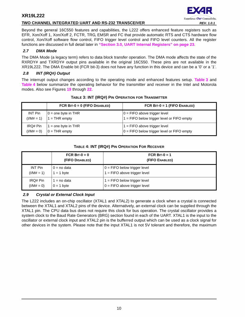
The interrupt output changes according to the operating mode and enhanced features setup. Table 3 and Table 4 below summarize the operating behavior for the transmitter and receiver in the Intel and Motorola modes. Also see Figures 19 through 22.
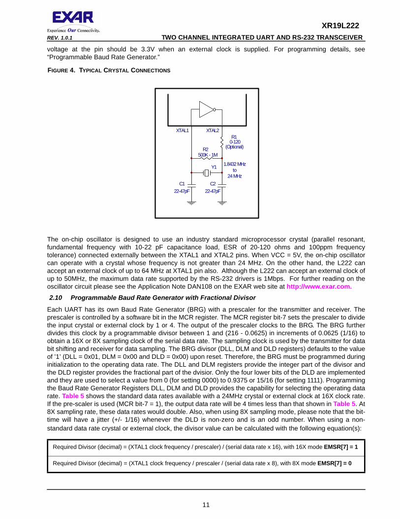
2.9 Crystal or External Clock InputThe L222 includes an on-chip oscillator (XTAL1 and XTAL2) to generate a clock when a crystal is connected between the XTAL1 and XTAL2 pins of the device. Alternatively, an external clock can be supplied through the XTAL1 pin. The CPU data bus does not require this clock for bus operation. The crystal oscillator provides a system clock to the Baud Rate Generators (BRG) section found in each of the UART. XTAL1 is the input to the oscillator or external clock input and XTAL2 pin is the bufferred output which can be used as a clock signal for other devices in the system. Please note that the input XTAL1 is not 5V tolerant and therefore, the maximum
TABLE 3: INT (IRQ#) PIN OPERATION FOR TRANSMITTER
FCR BIT-0 = 0 (FIFO DISABLED) FCR BIT-0 = 1 (FIFO ENABLED)
INT Pin(I/M# = 1)
0 = one byte in THR1 = THR empty
0 = FIFO above trigger level1 = FIFO below trigger level or FIFO empty
IRQ# Pin(I/M# = 0)
1 = one byte in THR0 = THR empty
1 = FIFO above trigger level0 = FIFO below trigger level or FIFO empty
TABLE 4: INT (IRQ#) PIN OPERATION FOR RECEIVER
FCR BIT-0 = 0 (FIFO DISABLED)
FCR BIT-0 = 1 (FIFO ENABLED)
INT Pin(I/M# = 1)
0 = no data1 = 1 byte
0 = FIFO below trigger level1 = FIFO above trigger level
IRQ# Pin(I/M# = 0)
1 = no data0 = 1 byte
1 = FIFO below trigger level0 = FIFO above trigger level
10
XR19L222REV. 1.0.1 TWO CHANNEL INTEGRATED UART AND RS-232 TRANSCEIVER
voltage at the pin should be 3.3V when an external clock is supplied. For programming details, see “Programmable Baud Rate Generator.”
The on-chip oscillator is designed to use an industry standard microprocessor crystal (parallel resonant, fundamental frequency with 10-22 pF capacitance load, ESR of 20-120 ohms and 100ppm frequency tolerance) connected externally between the XTAL1 and XTAL2 pins. When VCC = 5V, the on-chip oscillator can operate with a crystal whose frequency is not greater than 24 MHz. On the other hand, the L222 can accept an external clock of up to 64 MHz at XTAL1 pin also. Although the L222 can accept an external clock of up to 50MHz, the maximum data rate supported by the RS-232 drivers is 1Mbps. For further reading on the oscillator circuit please see the Application Note DAN108 on the EXAR web site at http://www.exar.com.2.10 Programmable Baud Rate Generator with Fractional Divisor
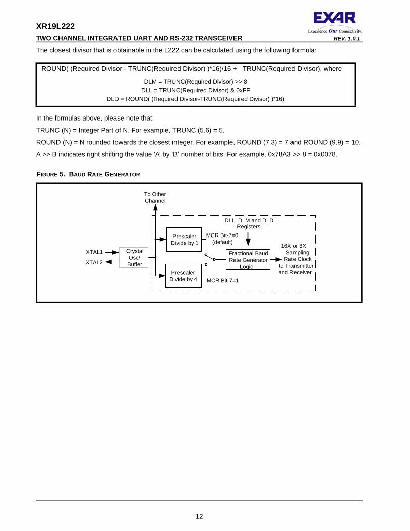
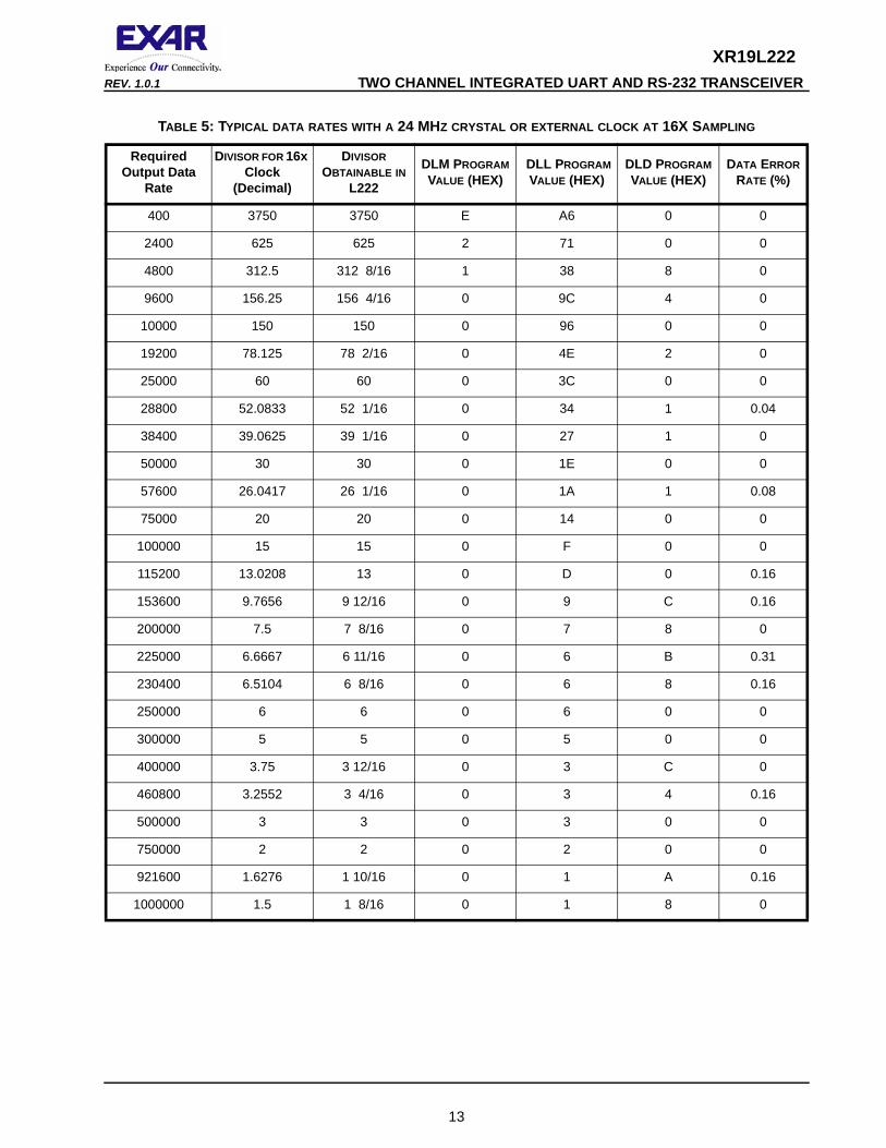
Each UART has its own Baud Rate Generator (BRG) with a prescaler for the transmitter and receiver. The prescaler is controlled by a software bit in the MCR register. The MCR register bit-7 sets the prescaler to divide the input crystal or external clock by 1 or 4. The output of the prescaler clocks to the BRG. The BRG further divides this clock by a programmable divisor between 1 and (216 - 0.0625) in increments of 0.0625 (1/16) to obtain a 16X or 8X sampling clock of the serial data rate. The sampling clock is used by the transmitter for data bit shifting and receiver for data sampling. The BRG divisor (DLL, DLM and DLD registers) defaults to the value of ’1’ (DLL = 0x01, DLM = 0x00 and DLD = 0x00) upon reset. Therefore, the BRG must be programmed during initialization to the operating data rate. The DLL and DLM registers provide the integer part of the divisor and the DLD register provides the fractional part of the dvisior. Only the four lower bits of the DLD are implemented and they are used to select a value from 0 (for setting 0000) to 0.9375 or 15/16 (for setting 1111). Programming the Baud Rate Generator Registers DLL, DLM and DLD provides the capability for selecting the operating data rate. Table 5 shows the standard data rates available with a 24MHz crystal or external clock at 16X clock rate. If the pre-scaler is used (MCR bit-7 = 1), the output data rate will be 4 times less than that shown in Table 5. At 8X sampling rate, these data rates would double. Also, when using 8X sampling mode, please note that the bit-time will have a jitter (+/- 1/16) whenever the DLD is non-zero and is an odd number. When using a non-standard data rate crystal or external clock, the divisor value can be calculated with the following equation(s):
FIGURE 4. TYPICAL CRYSTAL CONNECTIONS
Required Divisor (decimal) = (XTAL1 clock frequency / prescaler) / (serial data rate x 16), with 16X mode EMSR[7] = 1
Required Divisor (decimal) = (XTAL1 clock frequency / prescaler / (serial data rate x 8), with 8X mode EMSR[7] = 0
C122-47pF
C222-47pF
Y1 1.8432 MHzto
24 MHz
R10-120
(Optional)R2500K - 1M
XTAL1 XTAL2
11
XR19L222 TWO CHANNEL INTEGRATED UART AND RS-232 TRANSCEIVER REV. 1.0.1
The closest divisor that is obtainable in the L222 can be calculated using the following formula:
In the formulas above, please note that:
TRUNC (N) = Integer Part of N. For example, TRUNC (5.6) = 5.
ROUND (N) = N rounded towards the closest integer. For example, ROUND (7.3) = 7 and ROUND (9.9) = 10.
A >> B indicates right shifting the value ’A’ by ’B’ number of bits. For example, 0x78A3 >> 8 = 0x0078.
ROUND( (Required Divisor - TRUNC(Required Divisor) )*16)/16 + TRUNC(Required Divisor), where
DLM = TRUNC(Required Divisor) >> 8DLL = TRUNC(Required Divisor) & 0xFF
DLD = ROUND( (Required Divisor-TRUNC(Required Divisor) )*16)
FIGURE 5. BAUD RATE GENERATOR
XTAL1
XTAL2
CrystalOsc/Buffer
MCR Bit-7=0(default)
MCR Bit-7=1
DLL, DLM and DLDRegisters
PrescalerDivide by 1
PrescalerDivide by 4
16X or 8XSampling
Rate Clockto Transmitterand Receiver
To OtherChannel
Fractional BaudRate Generator
Logic
12
XR19L222REV. 1.0.1 TWO CHANNEL INTEGRATED UART AND RS-232 TRANSCEIVER
TABLE 5: TYPICAL DATA RATES WITH A 24 MHZ CRYSTAL OR EXTERNAL CLOCK AT 16X SAMPLING
Required Output Data
Rate
DIVISOR FOR 16x Clock
(Decimal)
DIVISOR OBTAINABLE IN
L222
DLM PROGRAM VALUE (HEX)
DLL PROGRAM VALUE (HEX)
DLD PROGRAM VALUE (HEX)
DATA ERROR RATE (%)
400 3750 3750 E A6 0 0
2400 625 625 2 71 0 0
4800 312.5 312 8/16 1 38 8 0
9600 156.25 156 4/16 0 9C 4 0
10000 150 150 0 96 0 0
19200 78.125 78 2/16 0 4E 2 0
25000 60 60 0 3C 0 0
28800 52.0833 52 1/16 0 34 1 0.04
38400 39.0625 39 1/16 0 27 1 0
50000 30 30 0 1E 0 0
57600 26.0417 26 1/16 0 1A 1 0.08
75000 20 20 0 14 0 0
100000 15 15 0 F 0 0
115200 13.0208 13 0 D 0 0.16
153600 9.7656 9 12/16 0 9 C 0.16
200000 7.5 7 8/16 0 7 8 0
225000 6.6667 6 11/16 0 6 B 0.31
230400 6.5104 6 8/16 0 6 8 0.16
250000 6 6 0 6 0 0
300000 5 5 0 5 0 0
400000 3.75 3 12/16 0 3 C 0
460800 3.2552 3 4/16 0 3 4 0.16
500000 3 3 0 3 0 0
750000 2 2 0 2 0 0
921600 1.6276 1 10/16 0 1 A 0.16
1000000 1.5 1 8/16 0 1 8 0
13
XR19L222 TWO CHANNEL INTEGRATED UART AND RS-232 TRANSCEIVER REV. 1.0.1
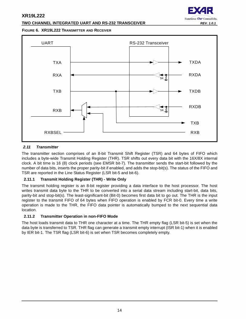
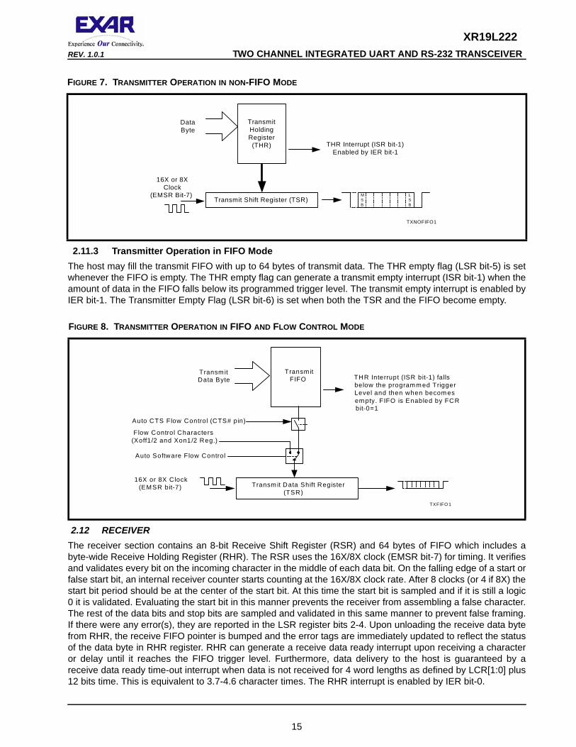
2.11 TransmitterThe transmitter section comprises of an 8-bit Transmit Shift Register (TSR) and 64 bytes of FIFO which includes a byte-wide Transmit Holding Register (THR). TSR shifts out every data bit with the 16X/8X internal clock. A bit time is 16 (8) clock periods (see EMSR bit-7). The transmitter sends the start-bit followed by the number of data bits, inserts the proper parity-bit if enabled, and adds the stop-bit(s). The status of the FIFO and TSR are reported in the Line Status Register (LSR bit-5 and bit-6). 2.11.1 Transmit Holding Register (THR) - Write Only
The transmit holding register is an 8-bit register providing a data interface to the host processor. The host writes transmit data byte to the THR to be converted into a serial data stream including start-bit, data bits, parity-bit and stop-bit(s). The least-significant-bit (Bit-0) becomes first data bit to go out. The THR is the input register to the transmit FIFO of 64 bytes when FIFO operation is enabled by FCR bit-0. Every time a write operation is made to the THR, the FIFO data pointer is automatically bumped to the next sequential data location.2.11.2 Transmitter Operation in non-FIFO Mode
The host loads transmit data to THR one character at a time. The THR empty flag (LSR bit-5) is set when the data byte is transferred to TSR. THR flag can generate a transmit empty interrupt (ISR bit-1) when it is enabled by IER bit-1. The TSR flag (LSR bit-6) is set when TSR becomes completely empty.
FIGURE 6. XR19L222 TRANSMITTER AND RECEIVER
TXA
RXA
TXB
RXB
RXB
TXB
UART RS-232 Transceiver
RXBSEL
TXDB
TXDA
5KRXDA
5KRXDB
14
XR19L222REV. 1.0.1 TWO CHANNEL INTEGRATED UART AND RS-232 TRANSCEIVER
2.11.3 Transmitter Operation in FIFO ModeThe host may fill the transmit FIFO with up to 64 bytes of transmit data. The THR empty flag (LSR bit-5) is set whenever the FIFO is empty. The THR empty flag can generate a transmit empty interrupt (ISR bit-1) when the amount of data in the FIFO falls below its programmed trigger level. The transmit empty interrupt is enabled by IER bit-1. The Transmitter Empty Flag (LSR bit-6) is set when both the TSR and the FIFO become empty.
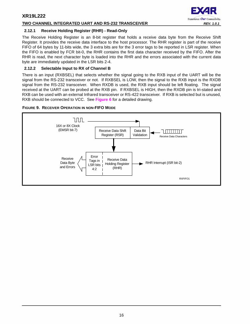
2.12 RECEIVERThe receiver section contains an 8-bit Receive Shift Register (RSR) and 64 bytes of FIFO which includes a byte-wide Receive Holding Register (RHR). The RSR uses the 16X/8X clock (EMSR bit-7) for timing. It verifies and validates every bit on the incoming character in the middle of each data bit. On the falling edge of a start or false start bit, an internal receiver counter starts counting at the 16X/8X clock rate. After 8 clocks (or 4 if 8X) the start bit period should be at the center of the start bit. At this time the start bit is sampled and if it is still a logic 0 it is validated. Evaluating the start bit in this manner prevents the receiver from assembling a false character. The rest of the data bits and stop bits are sampled and validated in this same manner to prevent false framing. If there were any error(s), they are reported in the LSR register bits 2-4. Upon unloading the receive data byte from RHR, the receive FIFO pointer is bumped and the error tags are immediately updated to reflect the status of the data byte in RHR register. RHR can generate a receive data ready interrupt upon receiving a character or delay until it reaches the FIFO trigger level. Furthermore, data delivery to the host is guaranteed by a receive data ready time-out interrupt when data is not received for 4 word lengths as defined by LCR[1:0] plus 12 bits time. This is equivalent to 3.7-4.6 character times. The RHR interrupt is enabled by IER bit-0.
FIGURE 7. TRANSMITTER OPERATION IN NON-FIFO MODE
FIGURE 8. TRANSMITTER OPERATION IN FIFO AND FLOW CONTROL MODE
TransmitHoldingRegister(THR)
Transmit Shift Register (TSR)
DataByte
LSB
MSB
THR Interrupt (ISR bit-1)Enabled by IER bit-1
TXNOFIFO1
16X or 8XClock
(EMSR Bit-7)
Transm it Data Shift Register(TSR)
TransmitData Byte THR Interrupt (ISR bit-1) falls
below the programm ed TriggerLevel and then when becom esem pty. FIFO is Enabled by FCRbit-0=1
TransmitFIFO
16X or 8X Clock(EMSR bit-7)
Auto CTS Flow Control (CTS# pin)
Auto Software Flow Control
Flow Control Characters(Xoff1/2 and Xon1/2 Reg.)
TXFIFO 1
15
XR19L222 TWO CHANNEL INTEGRATED UART AND RS-232 TRANSCEIVER REV. 1.0.1
2.12.1 Receive Holding Register (RHR) - Read-OnlyThe Receive Holding Register is an 8-bit register that holds a receive data byte from the Receive Shift Register. It provides the receive data interface to the host processor. The RHR register is part of the receive FIFO of 64 bytes by 11-bits wide, the 3 extra bits are for the 3 error tags to be reported in LSR register. When the FIFO is enabled by FCR bit-0, the RHR contains the first data character received by the FIFO. After the RHR is read, the next character byte is loaded into the RHR and the errors associated with the current data byte are immediately updated in the LSR bits 2-4.2.12.2 Selectable Input to RX of Channel B
There is an input (RXBSEL) that selects whether the signal going to the RXB input of the UART will be the signal from the RS-232 transceiver or not. If RXBSEL is LOW, then the signal to the RXB input is the RXDB signal from the RS-232 transceiver. When RXDB is used, the RXB input should be left floating. The signal received at the UART can be probed at the RXB pin. If RXBSEL is HIGH, then the RXDB pin is tri-stated and RXB can be used with an external Infrared transceiver or RS-422 transceiver. If RXB is selected but is unused, RXB should be connected to VCC. See Figure 6 for a detailed drawing.
FIGURE 9. RECEIVER OPERATION IN NON-FIFO MODE
Receive Data ShiftRegister (RSR)
ReceiveData Byteand Errors
RHR Interrupt (ISR bit-2)Receive Data
Holding Register(RHR)
RXFIFO1
16X or 8X Clock(EMSR bit-7)
Receive Data Characters
Data BitValidation
ErrorTags inLSR bits
4:2
16
XR19L222REV. 1.0.1 TWO CHANNEL INTEGRATED UART AND RS-232 TRANSCEIVER
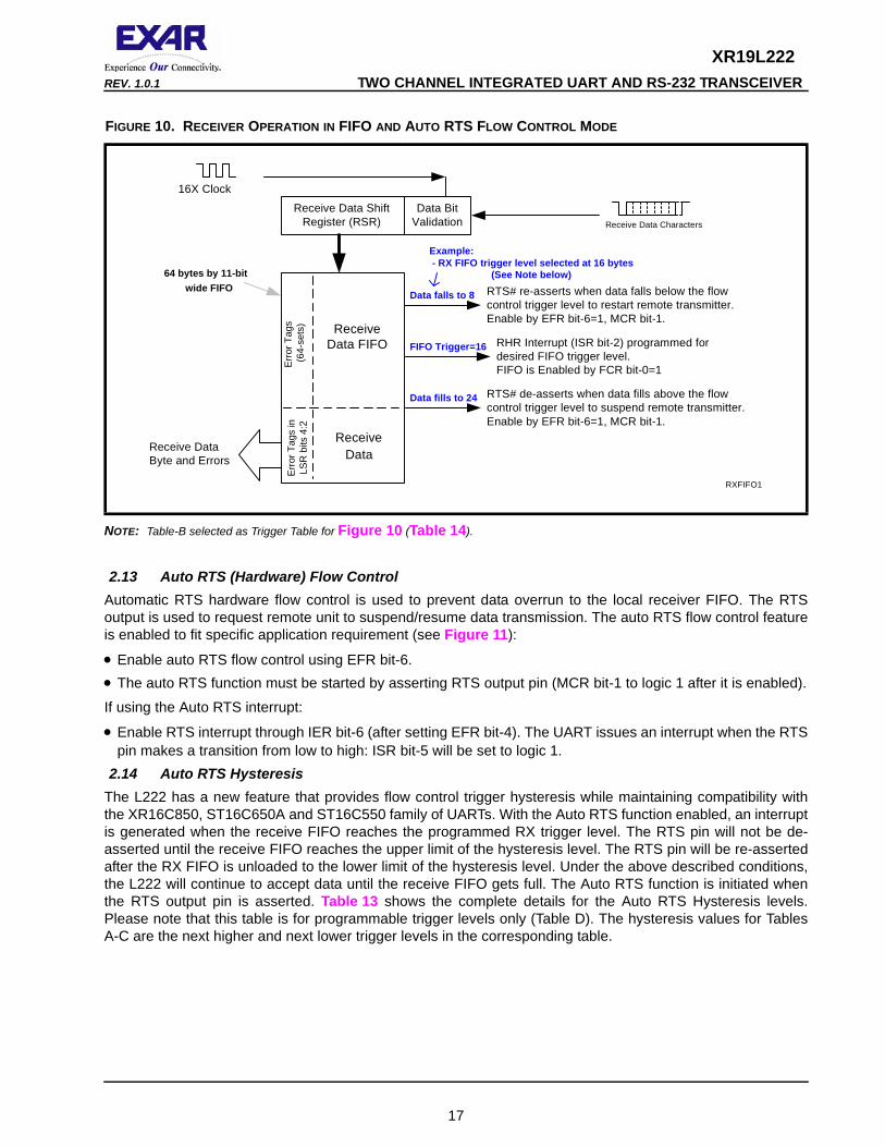
NOTE: Table-B selected as Trigger Table for Figure 10 (Table 14).
2.13 Auto RTS (Hardware) Flow ControlAutomatic RTS hardware flow control is used to prevent data overrun to the local receiver FIFO. The RTS output is used to request remote unit to suspend/resume data transmission. The auto RTS flow control feature is enabled to fit specific application requirement (see Figure 11):
• Enable auto RTS flow control using EFR bit-6.• The auto RTS function must be started by asserting RTS output pin (MCR bit-1 to logic 1 after it is enabled).
If using the Auto RTS interrupt:
• Enable RTS interrupt through IER bit-6 (after setting EFR bit-4). The UART issues an interrupt when the RTS pin makes a transition from low to high: ISR bit-5 will be set to logic 1.
2.14 Auto RTS HysteresisThe L222 has a new feature that provides flow control trigger hysteresis while maintaining compatibility with the XR16C850, ST16C650A and ST16C550 family of UARTs. With the Auto RTS function enabled, an interrupt is generated when the receive FIFO reaches the programmed RX trigger level. The RTS pin will not be de-asserted until the receive FIFO reaches the upper limit of the hysteresis level. The RTS pin will be re-asserted after the RX FIFO is unloaded to the lower limit of the hysteresis level. Under the above described conditions, the L222 will continue to accept data until the receive FIFO gets full. The Auto RTS function is initiated when the RTS output pin is asserted. Table 13 shows the complete details for the Auto RTS Hysteresis levels. Please note that this table is for programmable trigger levels only (Table D). The hysteresis values for Tables A-C are the next higher and next lower trigger levels in the corresponding table.
FIGURE 10. RECEIVER OPERATION IN FIFO AND AUTO RTS FLOW CONTROL MODE
Receive Data ShiftRegister (RSR)
RXFIFO1
16X Clock
Erro
r Tag
s(6
4-se
ts)
Erro
r Tag
s in
LSR
bits
4:2
64 bytes by 11-bitwide FIFO
Receive Data Characters
FIFO Trigger=16
Example: - RX FIFO trigger level selected at 16 bytes
(See Note below)
Data fills to 24
Data falls to 8
Data BitValidation
ReceiveData FIFO
ReceiveDataReceive Data
Byte and Errors
RHR Interrupt (ISR bit-2) programmed fordesired FIFO trigger level.FIFO is Enabled by FCR bit-0=1
RTS# de-asserts when data fills above the flowcontrol trigger level to suspend remote transmitter.Enable by EFR bit-6=1, MCR bit-1.
RTS# re-asserts when data falls below the flowcontrol trigger level to restart remote transmitter.Enable by EFR bit-6=1, MCR bit-1.
17
XR19L222 TWO CHANNEL INTEGRATED UART AND RS-232 TRANSCEIVER REV. 1.0.1
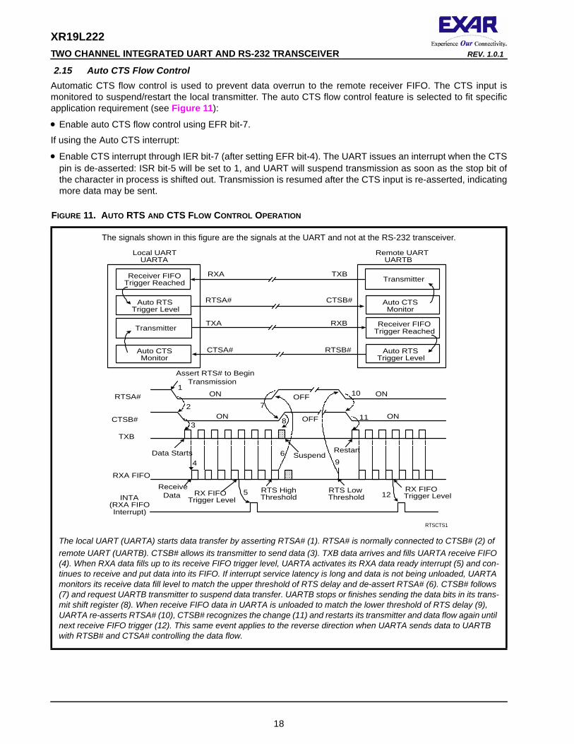
2.15 Auto CTS Flow ControlAutomatic CTS flow control is used to prevent data overrun to the remote receiver FIFO. The CTS input is monitored to suspend/restart the local transmitter. The auto CTS flow control feature is selected to fit specific application requirement (see Figure 11):
• Enable auto CTS flow control using EFR bit-7.
If using the Auto CTS interrupt:
• Enable CTS interrupt through IER bit-7 (after setting EFR bit-4). The UART issues an interrupt when the CTS pin is de-asserted: ISR bit-5 will be set to 1, and UART will suspend transmission as soon as the stop bit of the character in process is shifted out. Transmission is resumed after the CTS input is re-asserted, indicating more data may be sent.
FIGURE 11. AUTO RTS AND CTS FLOW CONTROL OPERATION
The signals shown in this figure are the signals at the UART and not at the RS-232 transceiver.
The local UART (UARTA) starts data transfer by asserting RTSA# (1). RTSA# is normally connected to CTSB# (2) of remote UART (UARTB). CTSB# allows its transmitter to send data (3). TXB data arrives and fills UARTA receive FIFO (4). When RXA data fills up to its receive FIFO trigger level, UARTA activates its RXA data ready interrupt (5) and con-tinues to receive and put data into its FIFO. If interrupt service latency is long and data is not being unloaded, UARTA monitors its receive data fill level to match the upper threshold of RTS delay and de-assert RTSA# (6). CTSB# follows (7) and request UARTB transmitter to suspend data transfer. UARTB stops or finishes sending the data bits in its trans-mit shift register (8). When receive FIFO data in UARTA is unloaded to match the lower threshold of RTS delay (9), UARTA re-asserts RTSA# (10), CTSB# recognizes the change (11) and restarts its transmitter and data flow again until next receive FIFO trigger (12). This same event applies to the reverse direction when UARTA sends data to UARTB with RTSB# and CTSA# controlling the data flow.
RTSA# CTSB#
RXA TXBTransmitterReceiver FIFO
Trigger Reached
Auto RTSTrigger Level
Auto CTSMonitor
RTSA#
TXB
RXA FIFO
CTSB#
Remote UARTUARTB
Local UARTUARTA
ON OFF ON
SuspendRestart
RTS HighThreshold
Data Starts
ON OFF ON
Assert RTS# to BeginTransmission
1
2
3
4
5
6
7
ReceiveData
RTS LowThreshold
9
10
11
Receiver FIFOTrigger Reached
Auto RTSTrigger Level
Transmitter
Auto CTSMonitor
RTSB#CTSA#
RXBTXA
INTA(RXA FIFOInterrupt)
RX FIFOTrigger Level
RX FIFOTrigger Level
8
12
RTSCTS1
18
XR19L222REV. 1.0.1 TWO CHANNEL INTEGRATED UART AND RS-232 TRANSCEIVER
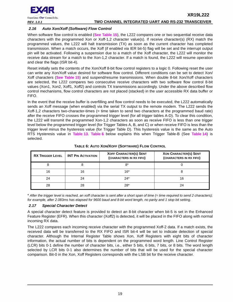
2.16 Auto Xon/Xoff (Software) Flow ControlWhen software flow control is enabled (See Table 15), the L222 compares one or two sequential receive data characters with the programmed Xon or Xoff-1,2 character value(s). If receive character(s) (RX) match the programmed values, the L222 will halt transmission (TX) as soon as the current character has completed transmission. When a match occurs, the Xoff (if enabled via IER bit-5) flag will be set and the interrupt output pin will be activated. Following a suspension due to a match of the Xoff character, the L222 will monitor the receive data stream for a match to the Xon-1,2 character. If a match is found, the L222 will resume operation and clear the flags (ISR bit-4). Reset initially sets the contents of the Xon/Xoff 8-bit flow control registers to a logic 0. Following reset the user can write any Xon/Xoff value desired for software flow control. Different conditions can be set to detect Xon/Xoff characters (See Table 15) and suspend/resume transmissions. When double 8-bit Xon/Xoff characters are selected, the L222 compares two consecutive receive characters with two software flow control 8-bit values (Xon1, Xon2, Xoff1, Xoff2) and controls TX transmissions accordingly. Under the above described flow control mechanisms, flow control characters are not placed (stacked) in the user accessible RX data buffer or FIFO. In the event that the receive buffer is overfilling and flow control needs to be executed, the L222 automatically sends an Xoff message (when enabled) via the serial TX output to the remote modem. The L222 sends the Xoff-1,2 characters two-character-times (= time taken to send two characters at the programmed baud rate) after the receive FIFO crosses the programmed trigger level (for all trigger tables A-D). To clear this condition, the L222 will transmit the programmed Xon-1,2 characters as soon as receive FIFO is less than one trigger level below the programmed trigger level (for Trigger Tables A, B, and C) or when receive FIFO is less than the trigger level minus the hysteresis value (for Trigger Table D). This hysteresis value is the same as the Auto RTS Hysteresis value in Table 13. Table 6 below explains this when Trigger Table-B (See Table 14) is selected.
* After the trigger level is reached, an xoff character is sent after a short span of time (= time required to send 2 characters); for example, after 2.083ms has elapsed for 9600 baud and 8-bit word length, no parity and 1 stop bit setting.
2.17 Special Character Detect A special character detect feature is provided to detect an 8-bit character when bit-5 is set in the Enhanced Feature Register (EFR). When this character (Xoff2) is detected, it will be placed in the FIFO along with normal incoming RX data. The L222 compares each incoming receive character with the programmed Xoff-2 data. If a match exists, the received data will be transferred to the RX FIFO and ISR bit-4 will be set to indicate detection of special character. Although the Internal Register Table shows Xon, Xoff Registers with eight bits of character information, the actual number of bits is dependent on the programmed word length. Line Control Register (LCR) bits 0-1 define the number of character bits, i.e., either 5 bits, 6 bits, 7 bits, or 8 bits. The word length selected by LCR bits 0-1 also determines the number of bits that will be used for the special character comparison. Bit-0 in the Xon, Xoff Registers corresponds with the LSB bit for the receive character.
TABLE 6: AUTO XON/XOFF (SOFTWARE) FLOW CONTROL
RX TRIGGER LEVEL INT PIN ACTIVATIONXOFF CHARACTER(S) SENT (CHARACTERS IN RX FIFO)
XON CHARACTER(S) SENT (CHARACTERS IN RX FIFO)
8 8 8* 0
16 16 16* 8
24 24 24* 16
28 28 28* 24
19
XR19L222 TWO CHANNEL INTEGRATED UART AND RS-232 TRANSCEIVER REV. 1.0.1
2.18 Sleep Modes and Power-Save Feature with Wake-Up InterruptThere are three levels of power management integrated in the L222. The device is low power with low operational and standby supply currents. In the Partial Sleep mode, the internal oscillator of the UART or charge pump of the RS-232 transceiver is turned off to reduce the power consumption. In the Full Sleep mode, both the oscillator and the charge pump are turned off. The Power-save mode provides additional power saving by isolating the UART address, data and control signals during Sleep mode to minimize the power consumption.2.18.1 Partial Sleep Mode
There are two different partial sleep modes. In the first mode, the UART is in sleep mode and the charge pump is active. In the other mode, the UART is still active but the charge pump is turned off. 2.18.1.1 UART in sleep mode, RS-232 transceiver active
If the ACP pin is LOW, then the charge pump for the RS-232 transceiver will always be active. But the UART portion in the L222 can still enter sleep mode if all of these conditions are satisfied:
■ no interrupts pending (ISR bit-0 = 1)■ the 16-bit divisor programmed in DLM and DLL registers is a non-zero value■ sleep mode is enabled (IER bit-4 = 1)■ modem inputs are not toggling (MSR bits 0-3 = 0)■ RXD input pin is idling LOW
The L222 stops its crystal oscillator to conserve power in this mode. The user can check the XTAL2 pin for no clock output as an indication that the device has entered the partial sleep mode.The UART portion in the L222 resumes normal operation or active mode by any of the following:
■ a receive data start bit transition on the RXD input (LOW to HIGH)■ a data byte is loaded to the transmitter, THR or FIFO ■ a change of logic state on any of the modem or general purpose serial inputs: i.e., any of the MSR bits 0-
3 shows a ’1’ If the sleep mode is enabled and the L222 is awakened by one of the conditions described above, an interrupt is issued by the L222 to signal to the CPU that it is awake. The lower nibble of the interrupt source register (ISR) will read a value of 0x1 for this interrupt and reading the ISR clears this interrupt. Since the same value (0x1) is also used to indicate no pending interrupt, users should exercise caution while using the sleep mode.The UART portion in the L222 will return to the sleep mode automatically after all interrupting conditions have been serviced and cleared. If the UART portion of the L222 is awakened by the modem inputs, a read to the MSR is required to reset the modem inputs. In any case, the sleep mode will not be entered while an interrupt is pending. The UART portion of the L222 will stay in the sleep mode of operation until it is disabled by setting IER bit-4 to a logic 0.
20
XR19L222REV. 1.0.1 TWO CHANNEL INTEGRATED UART AND RS-232 TRANSCEIVER
2.18.1.2 UART active, charge pump of RS-232 transceiver shut downIf the ACP pin is HIGH and the UART portion of the L222 is not in sleep mode, then the charge pump will automatically shut down to conserve power if the following conditions are true:
■ no activity on the TXD output signal■ modem input signals (RX, CTS, DSR, CD, RI) are LOW■ modem inputs have been idle for approximately 30 seconds
When these conditions are satisfied, the L222 shuts down the charge pump and tri-states the RS-232 drivers to conserve power. In this mode, the RS-232 receivers are fully active and the internal registers of the L222 can be accessed. The time for the charge pump to resume normal operation after exiting the sleep mode is typically 45µs. It will wake up by any of the following:
■ a receive data start bit transition on the RXD input (LOW to HIGH)■ a data byte is loaded to the transmitter, THR or FIFO■ a LOW to HIGH transition on any of the modem or general purpose serial inputs
Because the receivers are fully active when the charge pump is turned off, any data received will be transferred to/from the UART without any issues.2.18.2 Full Sleep Mode
In full sleep mode, the L222 shuts down the charge pump and the internal oscillator. The L222 enters the full sleep mode if the following conditions are satisfied:
■ the UART portion of the L222 is already in sleep mode (no output on XTAL2)■ the ACP (Autosleep for Charge Pump) pin is HIGH
When these conditions are satisfied, both the UART and the charge pump will be in the sleep mode. In this mode, the RS-232 receivers are fully active and the internal registers of the L222 can be accessed. The L222 exits the full sleep mode if either the ACP pin becomes LOW or the internal oscillator starts up. The time for the charge pump to resume normal operation after exiting the full sleep mode is typically 45µs.2.18.3 Power-Save Feature
This mode is in addition to the sleep mode and in this mode, the core logic of the L222 is isolated from the CPU interface. If the address lines, data bus lines, IOW#, IOR# and CS# remain steady when the L222 is in full sleep mode, the maximum current will be in the microamp range as specified in the DC Electrical Characteristics on page 42. However, if the input lines are floating or are toggling while the L222 is in sleep mode, the current can be up to 100 times more. If not using the Power-Save feature, an external buffer would be required to keep the address and data bus lines from toggling or floating to achieve the low current. But if the Power-Save feature is enabled (PwrSave pin connected to VCC), this will eliminate the need for an external buffer by internally isolating the address, data and control signals from other bus activities that could cause wasteful power drain (see Figure 1). The L222 enters Power-Save mode when this pin is connected to VCC, and the UART portion of the L222 is already in sleep mode.Since Power-Save mode isolates the address, data and control signals, the device will wake-up only by:
■ a receive data start bit transition, or■ a change of logic state on any of the modem or general purpose serial inputs: i.e., any of the MSR bits 0-
3 shows a ’1’ The L222 will return to the Power-Save mode automatically after a read to the MSR (to reset the modem inputs) and all interrupting conditions have been serviced and cleared. The L222 will stay in the Power-Save mode of operation until it is disabled by setting IER bit-4 to a logic 0 and/or the Power-Save pin is connected to GND.If the L222 is awakened by any one of the above conditions, it issues an interrupt as soon as the oscillator circuit is up and running and the device is ready to transmit/receive. This interrupt has the same encoding (bit-0 of ISR register = 1) as "no interrupt pending" and will clear when the ISR register is read. This will show up in the ISR register only if no other interrupts are enabled.
21
XR19L222 TWO CHANNEL INTEGRATED UART AND RS-232 TRANSCEIVER REV. 1.0.1
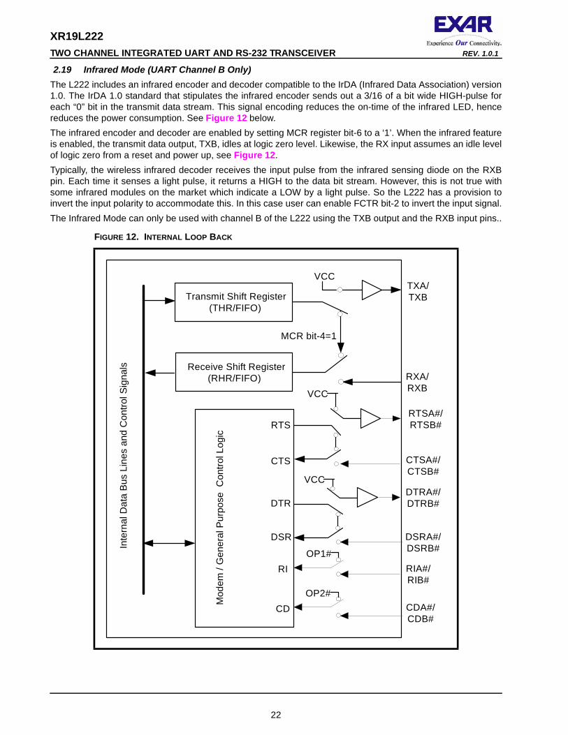
2.19 Infrared Mode (UART Channel B Only)The L222 includes an infrared encoder and decoder compatible to the IrDA (Infrared Data Association) version 1.0. The IrDA 1.0 standard that stipulates the infrared encoder sends out a 3/16 of a bit wide HIGH-pulse for each “0” bit in the transmit data stream. This signal encoding reduces the on-time of the infrared LED, hence reduces the power consumption. See Figure 12 below. The infrared encoder and decoder are enabled by setting MCR register bit-6 to a ‘1’. When the infrared feature is enabled, the transmit data output, TXB, idles at logic zero level. Likewise, the RX input assumes an idle level of logic zero from a reset and power up, see Figure 12. Typically, the wireless infrared decoder receives the input pulse from the infrared sensing diode on the RXB pin. Each time it senses a light pulse, it returns a HIGH to the data bit stream. However, this is not true with some infrared modules on the market which indicate a LOW by a light pulse. So the L222 has a provision to invert the input polarity to accommodate this. In this case user can enable FCTR bit-2 to invert the input signal.The Infrared Mode can only be used with channel B of the L222 using the TXB output and the RXB input pins..
FIGURE 12. INTERNAL LOOP BACK
TXA/TXB
RXA/RXB
Mod
em /
Gen
eral
Pur
pose
Con
trol L
ogic
Inte
rnal
Dat
a B
us L
ines
and
Con
trol S
igna
ls
RTSA#/RTSB#
MCR bit-4=1
VCC
VCC
Transmit Shift Register(THR/FIFO)
Receive Shift Register(RHR/FIFO)
CTSA#/CTSB#
DTRA#/DTRB#
DSRA#/DSRB#
RIA#/RIB#
CDA#/CDB#
OP1#
RTS
CTS
DTR
DSR
RI
CD
VCC
OP2#
22
XR19L222REV. 1.0.1 TWO CHANNEL INTEGRATED UART AND RS-232 TRANSCEIVER
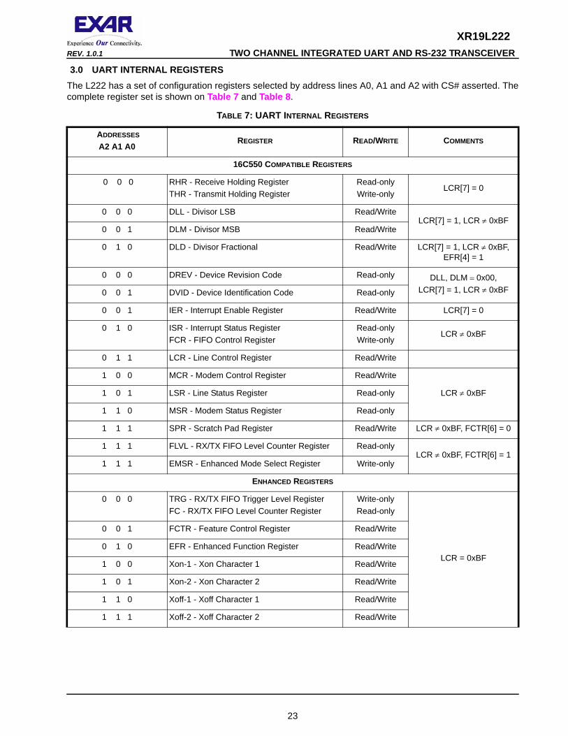
3.0 UART INTERNAL REGISTERS The L222 has a set of configuration registers selected by address lines A0, A1 and A2 with CS# asserted. The complete register set is shown on Table 7 and Table 8.
TABLE 7: UART INTERNAL REGISTERS
ADDRESSES
A2 A1 A0REGISTER READ/WRITE COMMENTS
16C550 COMPATIBLE REGISTERS
0 0 0 RHR - Receive Holding Register THR - Transmit Holding Register
Read-onlyWrite-only
LCR[7] = 0
0 0 0 DLL - Divisor LSB Read/WriteLCR[7] = 1, LCR ≠ 0xBF
0 0 1 DLM - Divisor MSB Read/Write
0 1 0 DLD - Divisor Fractional Read/Write LCR[7] = 1, LCR ≠ 0xBF, EFR[4] = 1
0 0 0 DREV - Device Revision Code Read-only DLL, DLM = 0x00, LCR[7] = 1, LCR ≠ 0xBF0 0 1 DVID - Device Identification Code Read-only
0 0 1 IER - Interrupt Enable Register Read/Write LCR[7] = 0
0 1 0 ISR - Interrupt Status RegisterFCR - FIFO Control Register
Read-onlyWrite-only
LCR ≠ 0xBF
0 1 1 LCR - Line Control Register Read/Write
1 0 0 MCR - Modem Control Register Read/Write
LCR ≠ 0xBF1 0 1 LSR - Line Status Register Read-only
1 1 0 MSR - Modem Status Register Read-only
1 1 1 SPR - Scratch Pad Register Read/Write LCR ≠ 0xBF, FCTR[6] = 0
1 1 1 FLVL - RX/TX FIFO Level Counter Register Read-onlyLCR ≠ 0xBF, FCTR[6] = 1
1 1 1 EMSR - Enhanced Mode Select Register Write-only
ENHANCED REGISTERS
0 0 0 TRG - RX/TX FIFO Trigger Level RegisterFC - RX/TX FIFO Level Counter Register
Write-onlyRead-only
LCR = 0xBF
0 0 1 FCTR - Feature Control Register Read/Write
0 1 0 EFR - Enhanced Function Register Read/Write
1 0 0 Xon-1 - Xon Character 1 Read/Write
1 0 1 Xon-2 - Xon Character 2 Read/Write
1 1 0 Xoff-1 - Xoff Character 1 Read/Write
1 1 1 Xoff-2 - Xoff Character 2 Read/Write
23
XR19L222 TWO CHANNEL INTEGRATED UART AND RS-232 TRANSCEIVER REV. 1.0.1
.
TABLE 8: INTERNAL REGISTERS DESCRIPTION. SHADED BITS ARE ENABLED WHEN EFR BIT-4=1
ADDRESS
A2-A0REG
NAME
READ/WRITE
BIT-7 BIT-6 BIT-5 BIT-4 BIT-3 BIT-2 BIT-1 BIT-0 COMMENT
16C550 Compatible Registers
0 0 0 RHR RD Bit-7 Bit-6 Bit-5 Bit-4 Bit-3 Bit-2 Bit-1 Bit-0
LCR[7]=0
0 0 0 THR WR Bit-7 Bit-6 Bit-5 Bit-4 Bit-3 Bit-2 Bit-1 Bit-0
0 0 1 IER RD/WR 0/ 0/ 0/ 0/ Modem Stat. Int. Enable
RX Line Stat. Int.
Enable
TX Empty
Int Enable
RX Data Int.
EnableCTS Int. Enable
RTS Int. Enable
Xoff Int. Enable
Sleep Mode
Enable
0 1 0 ISR RD FIFOs Enabled
FIFOs Enabled
0/ 0/ INT Source Bit-3
INT Source Bit-2
INT Source Bit-1
INT Source Bit-0
LCR ≠ 0xBF
INT Source Bit-5
INT Source
Bit-4
0 1 0 FCR WR RX FIFO Trigger
RX FIFO Trigger
0/ 0/ DMA Mode
Enable
TX FIFO Reset
RX FIFO Reset
FIFOs Enable
TX FIFO Trigger
TX FIFO Trigger
0 1 1 LCR RD/WR Divisor Enable
Set TX Break
Set Par-ity
Even Parity
Parity Enable
Stop Bits
Word LengthBit-1
Word LengthBit-0
1 0 0 MCR RD/WR 0/ 0/ 0/ Internal Lopback Enable
OP2#/INT Output Enable
Rsrvd(OP1#)
RTS# Output Control
DTR# Output Control
LCR ≠ 0xBF
BRG Pres-caler
IR Mode ENable
XonAny
1 0 1 LSR RD RX FIFO Global Error
THR & TSR
Empty
THR Empty
RX Break
RX Fram-ing Error
RX Parity Error
RX Over-run
Error
RX Data
Ready
1 1 0 MSR RD CD# Input
RI# Input
DSR# Input
CTS# Input
Delta CD#
Delta RI#
Delta DSR#
Delta CTS#
1 1 1 SPR RD/WR Bit-7 Bit-6 Bit-5 Bit-4 Bit-3 Bit-2 Bit-1 Bit-0 LCR ≠ 0xBFFCTR[6]=0
1 1 1 EMSR WR 16X Sam-pling Rate Mode
LSR Error Inter-rupt.
Imd/Dly#
AutoRTS Hyst. bit-3
AutoRTS Hyst. bit-2
Rsrvd Rsrvd Rx/Tx FIFO Count
Rx/Tx FIFO Count
LCR ≠ 0xBFFCTR[6]=1
1 1 1 FLVL RD Bit-7 Bit-6 Bit-5 Bit-4 Bit-3 Bit-2 Bit-1 Bit-0
24
XR19L222REV. 1.0.1 TWO CHANNEL INTEGRATED UART AND RS-232 TRANSCEIVER
4.0 INTERNAL REGISTER DESCRIPTIONS4.1 Receive Holding Register (RHR) - Read- Only
SEE ”RECEIVER” ON PAGE 15.4.2 Transmit Holding Register (THR) - Write-Only
SEE ”TRANSMITTER” ON PAGE 14.4.3 Interrupt Enable Register (IER) - Read/Write
The Interrupt Enable Register (IER) masks the interrupts from receive data ready, transmit empty, line status and modem status registers. These interrupts are reported in the Interrupt Status Register (ISR).
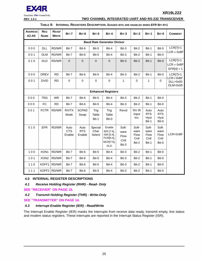
Baud Rate Generator Divisor
0 0 0 DLL RD/WR Bit-7 Bit-6 Bit-5 Bit-4 Bit-3 Bit-2 Bit-1 Bit-0 LCR[7]=1LCR ≠ 0xBF
0 0 1 DLM RD/WR Bit-7 Bit-6 Bit-5 Bit-4 Bit-3 Bit-2 Bit-1 Bit-0
0 1 0 DLD RD/WR 0 0 0 0 Bit-3 Bit-2 Bit-1 Bit-0 LCR[7]=1LCR ≠ 0xBFEFR[4] = 1
0 0 0 DREV RD Bit-7 Bit-6 Bit-5 Bit-4 Bit-3 Bit-2 Bit-1 Bit-0 LCR[7]=1 LCR ≠ 0xBF DLL=0x00 DLM=0x00
0 0 1 DVID RD 0 0 0 0 1 0 1 0
Enhanced Registers
0 0 0 TRG WR Bit-7 Bit-6 Bit-5 Bit-4 Bit-3 Bit-2 Bit-1 Bit-0
LCR=0XBF
0 0 0 FC RD Bit-7 Bit-6 Bit-5 Bit-4 Bit-3 Bit-2 Bit-1 Bit-0
0 0 1 FCTR RD/WR RX/TXMode
SCPADSwap
TrigTableBit-1
TrigTableBit-0
Rsrvd RX IR Input Inv.
Auto RTS Hyst Bit-1
Auto RTS Hyst Bit-0
0 1 0 EFR RD/WR Auto CTS
Enable
Auto RTS
Enable
Special Char
Select
Enable IER [7:4], ISR [5:4], FCR[5:4],MCR[7:5],
DLD
Soft-ware Flow CntlBit-3
Soft-ware Flow CntlBit-2
Soft-ware Flow CntlBit-1
Soft-ware Flow CntlBit-0
1 0 0 XON1 RD/WR Bit-7 Bit-6 Bit-5 Bit-4 Bit-3 Bit-2 Bit-1 Bit-0
1 0 1 XON2 RD/WR Bit-7 Bit-6 Bit-5 Bit-4 Bit-3 Bit-2 Bit-1 Bit-0
1 1 0 XOFF1 RD/WR Bit-7 Bit-6 Bit-5 Bit-4 Bit-3 Bit-2 Bit-1 Bit-0
1 1 1 XOFF2 RD/WR Bit-7 Bit-6 Bit-5 Bit-4 Bit-3 Bit-2 Bit-1 Bit-0
TABLE 8: INTERNAL REGISTERS DESCRIPTION. SHADED BITS ARE ENABLED WHEN EFR BIT-4=1
ADDRESS
A2-A0REG
NAME
READ/WRITE
BIT-7 BIT-6 BIT-5 BIT-4 BIT-3 BIT-2 BIT-1 BIT-0 COMMENT
25
XR19L222 TWO CHANNEL INTEGRATED UART AND RS-232 TRANSCEIVER REV. 1.0.1
4.3.1 IER versus Receive FIFO Interrupt Mode Operation
When the receive FIFO (FCR BIT-0 = 1) and receive interrupts (IER BIT-0 = 1) are enabled, the RHR interrupts (see ISR bits 2 and 3) status will reflect the following:
A. The receive data available interrupts are issued to the host when the FIFO has reached the programmed trigger level. It will be cleared when the FIFO drops below the programmed trigger level.
B. FIFO level will be reflected in the ISR register when the FIFO trigger level is reached. Both the ISR register status bit and the interrupt will be cleared when the FIFO drops below the trigger level.
C. The receive data ready bit (LSR BIT-0) is set as soon as a character is transferred from the shift register to the receive FIFO. It is reset when the FIFO is empty.
4.3.2 IER versus Receive/Transmit FIFO Polled Mode Operation
When FCR BIT-0 equals a logic 1 for FIFO enable; resetting IER bits 0-3 enables the XR19L222 in the FIFO polled mode of operation. Since the receiver and transmitter have separate bits in the LSR either or both can be used in the polled mode by selecting respective transmit or receive control bit(s).
A. LSR BIT-0 indicates there is data in RHR or RX FIFO.B. LSR BIT-1 indicates an overrun error has occurred and that data in the FIFO may not be valid.C. LSR BIT 2-4 provides the type of receive data errors encountered for the data byte in RHR, if any.D. LSR BIT-5 indicates THR is empty.E. LSR BIT-6 indicates when both the transmit FIFO and TSR are empty.F. LSR BIT-7 indicates a data error in at least one character in the RX FIFO.
IER[0]: RHR Interrupt Enable
The receive data ready interrupt will be issued when RHR has a data character in the non-FIFO mode or when the receive FIFO has reached the programmed trigger level in the FIFO mode.
• Logic 0 = Disable the receive data ready interrupt (default).
• Logic 1 = Enable the receiver data ready interrupt.
IER[1]: THR Interrupt Enable
This bit enables the Transmit Ready interrupt which is issued whenever the THR becomes empty in the non-FIFO mode or when data in the FIFO falls below the programmed trigger level in the FIFO mode. If the THR is empty when this bit is enabled, an interrupt will be generated.
• Logic 0 = Disable Transmit Ready interrupt (default).
• Logic 1 = Enable Transmit Ready interrupt.
IER[2]: Receive Line Status Interrupt Enable
If any of the LSR register bits 1, 2, 3 or 4 is a logic 1, it will generate an interrupt to inform the host controller about the error status of the current data byte in FIFO. LSR bit-1 generates an interrupt immediately when the character has been received. LSR bits 2-4 generate an interrupt when the character with errors is read out of the FIFO (default). Instead, LSR bits 2-4 can be programmed to generate an interrupt immediately, by setting EMSR bit-6 to a logic 1.
• Logic 0 = Disable the receiver line status interrupt (default).
• Logic 1 = Enable the receiver line status interrupt.
IER[3]: Modem Status Interrupt Enable
• Logic 0 = Disable the modem status register interrupt (default).
• Logic 1 = Enable the modem status register interrupt.
26
XR19L222REV. 1.0.1 TWO CHANNEL INTEGRATED UART AND RS-232 TRANSCEIVER
IER[4]: Sleep Mode Enable (requires EFR bit-4 = 1)
• Logic 0 = Disable Sleep Mode (default).
• Logic 1 = Enable Sleep Mode. See Sleep Mode section for further details.
IER[5]: Xoff Interrupt Enable (requires EFR bit-4=1)
• Logic 0 = Disable the software flow control, receive Xoff interrupt (default).
• Logic 1 = Enable the software flow control, receive Xoff interrupt. See Software Flow Control section for details.
IER[6]: RTS# Output Interrupt Enable (requires EFR bit-4=1)
• Logic 0 = Disable the RTS# interrupt (default).
• Logic 1 = Enable the RTS# interrupt. The UART issues an interrupt when the RTS# pin makes a transition from low to high.
IER[7]: CTS# Input Interrupt Enable (requires EFR bit-4=1)
• Logic 0 = Disable the CTS# interrupt (default).
• Logic 1 = Enable the CTS# interrupt. The UART issues an interrupt when CTS# pin makes a transition from low to high.
4.4 Interrupt Status Register (ISR) - Read-Only
The UART provides multiple levels of prioritized interrupts to minimize external software interaction. The Interrupt Status Register (ISR) provides the user with six interrupt status bits. Performing a read cycle on the ISR will give the user the current highest pending interrupt level to be serviced, others are queued up to be serviced next. No other interrupts are acknowledged until the pending interrupt is serviced. The Interrupt Source Table, Table 9, shows the data values (bit 0-5) for the interrupt priority levels and the interrupt sources associated with each of these interrupt levels.
4.4.1 Interrupt Generation:
• LSR is by any of the LSR bits 1, 2, 3 and 4.
• RXRDY is by RX trigger level.
• RXRDY Time-out is by a 4-char plus 12 bits delay timer.
• TXRDY is by TX trigger level or TX FIFO empty (or transmitter empty in auto RS-485 control).
• MSR is by any of the MSR bits 0, 1, 2 and 3.
• Receive Xoff/Special character is by detection of a Xoff or Special character.
• CTS# is when its transmitter toggles the input pin (from LOW to HIGH) during auto CTS flow control.
• RTS# is when its receiver toggles the output pin (from LOW to HIGH) during auto RTS flow control.
• Wake-up Indicator is when the UART comes out of sleep mode.
27
XR19L222 TWO CHANNEL INTEGRATED UART AND RS-232 TRANSCEIVER REV. 1.0.1
4.4.2 Interrupt Clearing:
• LSR interrupt is cleared by a read to the LSR register.
• RXRDY interrupt is cleared by reading data until FIFO falls below the trigger level.
• RXRDY Time-out interrupt is cleared by reading RHR.
• TXRDY interrupt is cleared by a read to the ISR register or writing to THR.
• MSR interrupt is cleared by a read to the MSR register.
• Xoff interrupt is cleared by a read to ISR or when Xon character(s) is received.
• Special character interrupt is cleared by a read to ISR or after the next character is received.
• RTS# and CTS# flow control interrupts are cleared by a read to the MSR register.
• Wake-up Indicator is cleared by a read to the ISR register.]
ISR[0]: Interrupt Status
• Logic 0 = An interrupt is pending and the ISR contents may be used as a pointer to the appropriate interrupt service routine.
• Logic 1 = No interrupt pending (default condition) or the device has come out of sleep mode.
ISR[3:1]: Interrupt Status
These bits indicate the source for a pending interrupt at interrupt priority levels (See Interrupt Source Table 9).
ISR[4]: Xoff or Special Character Interrupt Status (requires EFR bit-4=1)
This bit is enabled when IER[5] = 1. ISR bit-4 indicates that the receiver detected a data match of the Xoff character(s) or special character (XOFF2).
ISR[5]: RTS#/CTS# Interrupt Status (requires EFR bit-4=1)
This bit is enabled when IER[7] = 1 or IER[6] = 1. ISR bit-5 indicates that the CTS# or RTS# has been de-asserted.
ISR[7:6]: FIFO Enable Status
These bits are set to a logic 0 when the FIFOs are disabled. They are set to a logic 1 when the FIFOs are enabled.
TABLE 9: INTERRUPT SOURCE AND PRIORITY LEVEL
PRIORITY ISR REGISTER STATUS BITS SOURCE OF INTERRUPT
LEVEL BIT-5 BIT-4 BIT-3 BIT-2 BIT-1 BIT-0
1 0 0 0 1 1 0 LSR (Receiver Line Status Register)
2 0 0 1 1 0 0 RXRDY (Receive Data Time-out)
3 0 0 0 1 0 0 RXRDY (Received Data Ready)
4 0 0 0 0 1 0 TXRDY (Transmit Ready)
5 0 0 0 0 0 0 MSR (Modem Status Register)
6 0 1 0 0 0 0 RXRDY (Received Xoff or Special character)
7 1 0 0 0 0 0 CTS#, RTS# change of state
- 0 0 0 0 0 1 None (default) or Wake-up Indicator
28
XR19L222REV. 1.0.1 TWO CHANNEL INTEGRATED UART AND RS-232 TRANSCEIVER
4.5 FIFO Control Register (FCR) - Write-Only
This register is used to enable the FIFOs, clear the FIFOs, set the transmit/receive FIFO trigger levels, and select the DMA mode. The DMA, and FIFO modes are defined as follows:
FCR[0]: TX and RX FIFO Enable
• Logic 0 = Disable the transmit and receive FIFO (default).
• Logic 1 = Enable the transmit and receive FIFOs. This bit must be set to logic 1 when other FCR bits are written or they will not be programmed.
FCR[1]: RX FIFO Reset
This bit is only active when FCR bit-0 is a ‘1’.
• Logic 0 = No receive FIFO reset (default)
• Logic 1 = Reset the receive FIFO pointers and FIFO level counter logic (the receive shift register is not cleared or altered). This bit will return to a logic 0 after resetting the FIFO.
FCR[2]: TX FIFO Reset
This bit is only active when FCR bit-0 is a ‘1’.
• Logic 0 = No transmit FIFO reset (default).
• Logic 1 = Reset the transmit FIFO pointers and FIFO level counter logic (the transmit shift register is not cleared or altered). This bit will return to a logic 0 after resetting the FIFO.
FCR[3]: DMA Mode Select
Controls the behavior of the TXRDY# and RXRDY# pins. See DMA operation section for details.
• Logic 0 = Normal Operation (default).
• Logic 1 = DMA Mode.
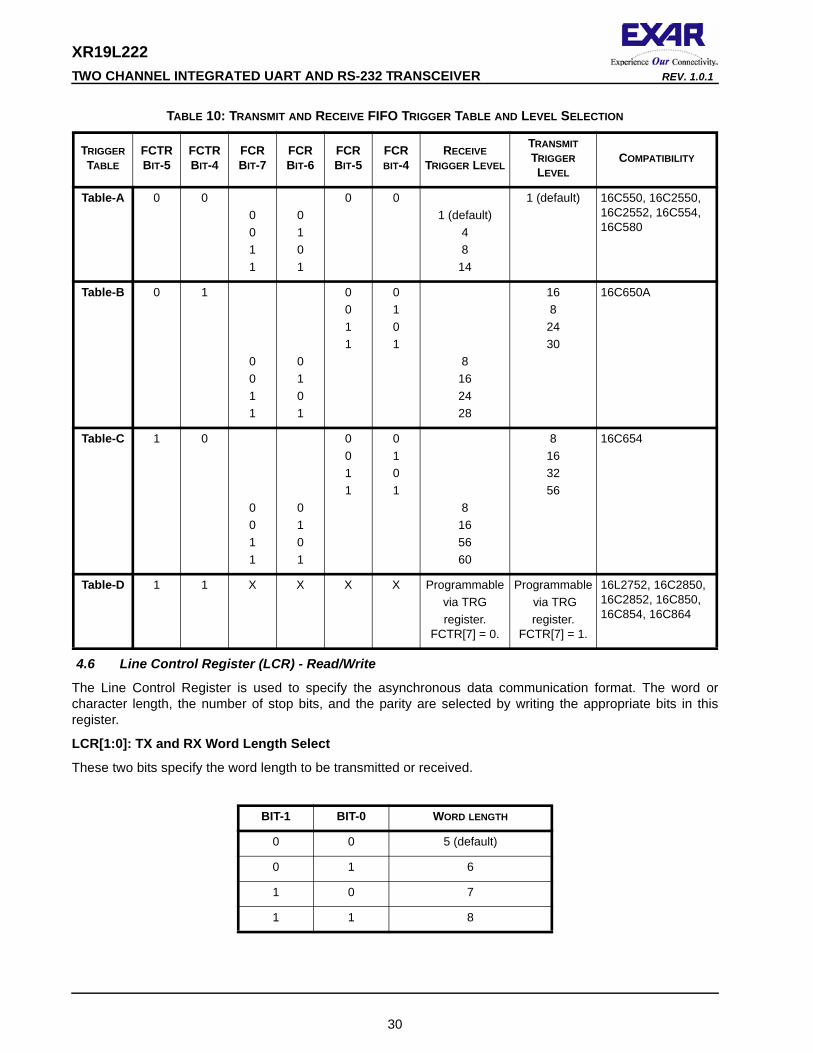
FCR[5:4]: Transmit FIFO Trigger Select (requires EFR bit-4=1)
(logic 0 = default, TX trigger level = 1)
These 2 bits set the trigger level for the transmit FIFO. The UART will issue a transmit interrupt when the number of characters in the FIFO falls below the selected trigger level, or when it gets empty in case that the FIFO did not get filled over the trigger level on last re-load. Table 10 below shows the selections. EFR bit-4 must be set to ‘1’ before these bits can be accessed. Note that the receiver and the transmitter cannot use different trigger tables. Whichever selection is made last applies to both the RX and TX side.
FCR[7:6]: Receive FIFO Trigger Select
(logic 0 = default, RX trigger level =1)
The FCTR Bits 5-4 are associated with these 2 bits. These 2 bits are used to set the trigger level for the receive FIFO. The UART will issue a receive interrupt when the number of the characters in the FIFO crosses the trigger level. Table 10 shows the complete selections. Note that the receiver and the transmitter cannot use different trigger tables. Whichever selection is made last applies to both the RX and TX side.
29
XR19L222 TWO CHANNEL INTEGRATED UART AND RS-232 TRANSCEIVER REV. 1.0.1
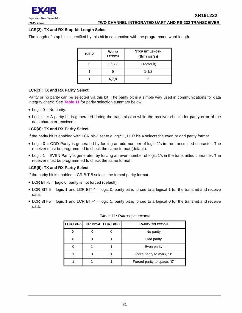
4.6 Line Control Register (LCR) - Read/Write
The Line Control Register is used to specify the asynchronous data communication format. The word or character length, the number of stop bits, and the parity are selected by writing the appropriate bits in this register.
LCR[1:0]: TX and RX Word Length Select
These two bits specify the word length to be transmitted or received.
TABLE 10: TRANSMIT AND RECEIVE FIFO TRIGGER TABLE AND LEVEL SELECTION
TRIGGER TABLE
FCTR BIT-5
FCTR BIT-4
FCR BIT-7
FCR BIT-6
FCR BIT-5
FCR BIT-4
RECEIVE TRIGGER LEVEL
TRANSMIT TRIGGER LEVEL
COMPATIBILITY
Table-A 0 00011
0101
0 01 (default)
48
14
1 (default) 16C550, 16C2550, 16C2552, 16C554, 16C580
Table-B 0 1
0011
0101
0011
0101
8162428
1682430
16C650A
Table-C 1 0
0011
0101
0011
0101
8165660
8163256
16C654
Table-D 1 1 X X X X Programmablevia TRG register.
FCTR[7] = 0.
Programmable via TRG register.
FCTR[7] = 1.
16L2752, 16C2850, 16C2852, 16C850, 16C854, 16C864
BIT-1 BIT-0 WORD LENGTH
0 0 5 (default)
0 1 6
1 0 7
1 1 8
30
XR19L222REV. 1.0.1 TWO CHANNEL INTEGRATED UART AND RS-232 TRANSCEIVER
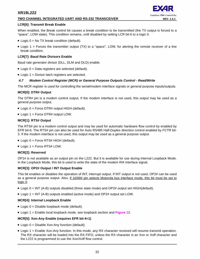
LCR[2]: TX and RX Stop-bit Length Select
The length of stop bit is specified by this bit in conjunction with the programmed word length.
LCR[3]: TX and RX Parity Select
Parity or no parity can be selected via this bit. The parity bit is a simple way used in communications for data integrity check. See Table 11 for parity selection summary below.
• Logic 0 = No parity.
• Logic 1 = A parity bit is generated during the transmission while the receiver checks for parity error of the data character received.
LCR[4]: TX and RX Parity Select
If the parity bit is enabled with LCR bit-3 set to a logic 1, LCR bit-4 selects the even or odd parity format.
• Logic 0 = ODD Parity is generated by forcing an odd number of logic 1’s in the transmitted character. The receiver must be programmed to check the same format (default).
• Logic 1 = EVEN Parity is generated by forcing an even number of logic 1’s in the transmitted character. The receiver must be programmed to check the same format.
LCR[5]: TX and RX Parity Select
If the parity bit is enabled, LCR BIT-5 selects the forced parity format.
• LCR BIT-5 = logic 0, parity is not forced (default).
• LCR BIT-5 = logic 1 and LCR BIT-4 = logic 0, parity bit is forced to a logical 1 for the transmit and receive data.
• LCR BIT-5 = logic 1 and LCR BIT-4 = logic 1, parity bit is forced to a logical 0 for the transmit and receive data.
BIT-2 WORD LENGTH
STOP BIT LENGTH
(BIT TIME(S))
0 5,6,7,8 1 (default)
1 5 1-1/2
1 6,7,8 2
TABLE 11: PARITY SELECTION
LCR BIT-5 LCR BIT-4 LCR BIT-3 PARITY SELECTION
X X 0 No parity
0 0 1 Odd parity
0 1 1 Even parity
1 0 1 Force parity to mark, “1”
1 1 1 Forced parity to space, “0”
31
XR19L222 TWO CHANNEL INTEGRATED UART AND RS-232 TRANSCEIVER REV. 1.0.1
LCR[6]: Transmit Break Enable
When enabled, the Break control bit causes a break condition to be transmitted (the TX output is forced to a “space", LOW state). This condition remains, until disabled by setting LCR bit-6 to a logic 0.
• Logic 0 = No TX break condition (default).
• Logic 1 = Forces the transmitter output (TX) to a “space”, LOW, for alerting the remote receiver of a line break condition.
LCR[7]: Baud Rate Divisors Enable
Baud rate generator divisor (DLL, DLM and DLD) enable.
• Logic 0 = Data registers are selected (default).
• Logic 1 = Divisor latch registers are selected.
4.7 Modem Control Register (MCR) or General Purpose Outputs Control - Read/Write
The MCR register is used for controlling the serial/modem interface signals or general purpose inputs/outputs.
MCR[0]: DTR# Output
The DTR# pin is a modem control output. If the modem interface is not used, this output may be used as a general purpose output.
• Logic 0 = Force DTR# output HIGH (default).
• Logic 1 = Force DTR# output LOW.
MCR[1]: RTS# Output
The RTS# pin is a modem control output and may be used for automatic hardware flow control by enabled by EFR bit-6. The RTS# pin can also be used for Auto RS485 Half-Duplex direction control enabled by FCTR bit-3. If the modem interface is not used, this output may be used as a general purpose output.
• Logic 0 = Force RTS# HIGH (default).
• Logic 1 = Force RTS# LOW.
MCR[2]: Reserved
OP1# is not available as an output pin on the L222. But it is available for use during Internal Loopback Mode. In the Loopback Mode, this bit is used to write the state of the modem RI# interface signal.
MCR[3]: OP2# Output / INT Output Enable
This bit enables or disables the operation of INT, interrupt output. If INT output is not used, OP2# can be used as a general purpose output. Also, if 16/68# pin selects Motorola bus interface mode, this bit must be set to logic 0.
• Logic 0 = INT (A-B) outputs disabled (three state mode) and OP2# output set HIGH(default).
• Logic 1 = INT (A-B) outputs enabled (active mode) and OP2# output set LOW.
MCR[4]: Internal Loopback Enable
• Logic 0 = Disable loopback mode (default).
• Logic 1 = Enable local loopback mode, see loopback section and Figure 12.
MCR[5]: Xon-Any Enable (requires EFR bit-4=1)
• Logic 0 = Disable Xon-Any function (default).
• Logic 1 = Enable Xon-Any function. In this mode, any RX character received will resume transmit operation. The RX character will be loaded into the RX FIFO, unless the RX character is an Xon or Xoff character and the L222 is programmed to use the Xon/Xoff flow control.
32
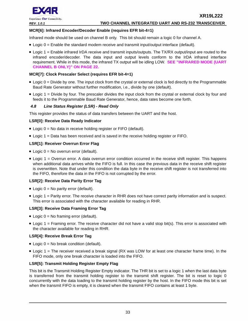
XR19L222REV. 1.0.1 TWO CHANNEL INTEGRATED UART AND RS-232 TRANSCEIVER
MCR[6]: Infrared Encoder/Decoder Enable (requires EFR bit-4=1)
Infrared mode should be used on channel B only. This bit should remain a logic 0 for channel A.
• Logic 0 = Enable the standard modem receive and transmit input/output interface (default).
• Logic 1 = Enable infrared IrDA receive and transmit inputs/outputs. The TX/RX output/input are routed to the infrared encoder/decoder. The data input and output levels conform to the IrDA infrared interface requirement. While in this mode, the infrared TX output will be idling LOW. SEE ”INFRARED MODE (UART CHANNEL B ONLY)” ON PAGE 22.
MCR[7]: Clock Prescaler Select (requires EFR bit-4=1)
• Logic 0 = Divide by one. The input clock from the crystal or external clock is fed directly to the Programmable Baud Rate Generator without further modification, i.e., divide by one (default).
• Logic 1 = Divide by four. The prescaler divides the input clock from the crystal or external clock by four and feeds it to the Programmable Baud Rate Generator, hence, data rates become one forth.
4.8 Line Status Register (LSR) - Read Only
This register provides the status of data transfers between the UART and the host.
LSR[0]: Receive Data Ready Indicator
• Logic 0 = No data in receive holding register or FIFO (default).
• Logic 1 = Data has been received and is saved in the receive holding register or FIFO.
LSR[1]: Receiver Overrun Error Flag
• Logic 0 = No overrun error (default).
• Logic 1 = Overrun error. A data overrun error condition occurred in the receive shift register. This happens when additional data arrives while the FIFO is full. In this case the previous data in the receive shift register is overwritten. Note that under this condition the data byte in the receive shift register is not transferred into the FIFO, therefore the data in the FIFO is not corrupted by the error.
LSR[2]: Receive Data Parity Error Tag
• Logic 0 = No parity error (default).
• Logic 1 = Parity error. The receive character in RHR does not have correct parity information and is suspect. This error is associated with the character available for reading in RHR.
LSR[3]: Receive Data Framing Error Tag
• Logic 0 = No framing error (default).
• Logic 1 = Framing error. The receive character did not have a valid stop bit(s). This error is associated with the character available for reading in RHR.
LSR[4]: Receive Break Error Tag
• Logic 0 = No break condition (default).
• Logic 1 = The receiver received a break signal (RX was LOW for at least one character frame time). In the FIFO mode, only one break character is loaded into the FIFO.
LSR[5]: Transmit Holding Register Empty Flag
This bit is the Transmit Holding Register Empty indicator. The THR bit is set to a logic 1 when the last data byte is transferred from the transmit holding register to the transmit shift register. The bit is reset to logic 0 concurrently with the data loading to the transmit holding register by the host. In the FIFO mode this bit is set when the transmit FIFO is empty, it is cleared when the transmit FIFO contains at least 1 byte.
33
XR19L222 TWO CHANNEL INTEGRATED UART AND RS-232 TRANSCEIVER REV. 1.0.1
LSR[6]: THR and TSR Empty Flag
This bit is set to a logic 1 whenever the transmitter goes idle. It is set to logic 0 whenever either the THR or TSR contains a data character. In the FIFO mode this bit is set to a logic 1 whenever the transmit FIFO and transmit shift register are both empty.
LSR[7]: Receive FIFO Data Error Flag
• Logic 0 = No FIFO error (default).
• Logic 1 = A global indicator for the sum of all error bits in the RX FIFO. At least one parity error, framing error or break indication is in the FIFO data. This bit clears when there is no more error(s) in any of the bytes in the RX FIFO.
4.9 Modem Status Register (MSR) - Read Only
This register provides the current state of the modem interface input signals. Lower four bits of this register are used to indicate the changed information. These bits are set to a logic 1 whenever a signal from the modem changes state. These bits may be used for general purpose inputs when they are not used with modem signals.
MSR[0]: Delta CTS# Input Flag
• Logic 0 = No change on CTS# input (default).
• Logic 1 = The CTS# input has changed state since the last time it was monitored. A modem status interrupt will be generated if MSR interrupt is enabled (IER bit-3).
MSR[1]: Delta DSR# Input Flag
• Logic 0 = No change on DSR# input (default).
• Logic 1 = The DSR# input has changed state since the last time it was monitored. A modem status interrupt will be generated if MSR interrupt is enabled (IER bit-3).
MSR[2]: Delta RI# Input Flag
• Logic 0 = No change on RI# input (default).
• Logic 1 = The RI# input has changed from a LOW to HIGH, ending of the ringing signal. A modem status interrupt will be generated if MSR interrupt is enabled (IER bit-3).
MSR[3]: Delta CD# Input Flag
• Logic 0 = No change on CD# input (default).
• Logic 1 = Indicates that the CD# input has changed state since the last time it was monitored. A modem status interrupt will be generated if MSR interrupt is enabled (IER bit-3).
MSR[4]: CTS Input Status
CTS# pin may function as automatic hardware flow control signal input if it is enabled and selected by Auto CTS (EFR bit-7). Auto CTS flow control allows starting and stopping of local data transmissions based on the modem CTS# signal. A HIGH on the CTS# pin will stop UART transmitter as soon as the current character has finished transmission, and a LOW will resume data transmission. Normally MSR bit-4 bit is the complement of the CTS# input. However in the loopback mode, this bit is equivalent to the RTS# bit in the MCR register. The CTS# input may be used as a general purpose input when the modem interface is not used.
MSR[5]: DSR Input Status
Normally this bit is the complement of the DSR# input. In the loopback mode, this bit is equivalent to the DTR# bit in the MCR register. The DSR# input may be used as a general purpose input when the modem interface is not used.
34
XR19L222REV. 1.0.1 TWO CHANNEL INTEGRATED UART AND RS-232 TRANSCEIVER
35
MSR[6]: RI Input Status
Normally this bit is the complement of the RI# input. In the loopback mode this bit is equivalent to bit-2 in the MCR register. The RI# input may be used as a general purpose input when the modem interface is not used.
MSR[7]: CD Input Status
Normally this bit is the complement of the CD# input. In the loopback mode this bit is equivalent to bit-3 in the MCR register. The CD# input may be used as a general purpose input when the modem interface is not used.
4.10 Scratch Pad Register (SPR) - Read/Write
This is a 8-bit general purpose register for the user to store temporary data. The content of this register is preserved during sleep mode but becomes 0xFF (default) after a reset or a power off-on cycle.
4.11 Enhanced Mode Select Register (EMSR)
This register replaces SPR (during a Write) and is accessible only when FCTR[6] = 1.
EMSR[1:0]: Receive/Transmit FIFO Level Count (Write-Only)
When Scratchpad Swap (FCTR[6]) is asserted, EMSR bits 1-0 controls what mode the FIFO Level Counter is operating in.
During Alternate RX/TX FIFO Level Counter Mode, the first value read after EMSR bits 1-0 have been asserted will always be the RX FIFO Level Counter. The second value read will correspond with the TX FIFO Level Counter. The next value will be the RX FIFO Level Counter again, then the TX FIFO Level Counter and so on and so forth.
EMSR[3:2]: Reserved
EMSR[5:4]: Extended RTS Hysteresis
TABLE 12: SCRATCHPAD SWAP SELECTION
FCTR[6] EMSR[1] EMSR[0] Scratchpad is
0 X X Scratchpad
1 X 0 RX FIFO Level Counter Mode
1 0 1 TX FIFO Level Counter Mode
1 1 1 Alternate RX/TX FIFO Counter Mode
TABLE 13: AUTO RTS HYSTERESIS
EMSR BIT-5
EMSR BIT-4
FCTR BIT-1
FCTR BIT-0
RTS# HYSTERESIS
(CHARACTERS)
0000
0000
0011
0101
0±4±6±8
0000
1111
0011
0101
±8±16±24±32
XR19L222 TWO CHANNEL INTEGRATED UART AND RS-232 TRANSCEIVER REV. 1.0.1
EMSR[6]: LSR Interrupt Mode
• Logic 0 = LSR Interrupt Delayed (for 16C2550 compatibility, default). LSR bits 2, 3, and 4 will generate an interrupt when the character with the error is in the RHR.
• Logic 1 = LSR Interrupt Immediate. LSR bits 2, 3, and 4 will generate an interrupt as soon as the character is received into the FIFO.
EMSR[7]: 16X Sampling Rate Mode
Logic 0 = 8X Sampling Rate.
Logic 1 = 16X Sampling Rate (default).
4.12 FIFO Level Register (FLVL) - Read-Only
The FIFO Level Register replaces the Scratchpad Register (during a Read) when FCTR[6] = 1. Note that this is not identical to the FIFO Data Count Register which can be accessed when LCR = 0xBF.
FLVL[7:0]: FIFO Level Register
This register provides the FIFO counter level for the RX FIFO or the TX FIFO or both depending on EMSR[1:0]. See Table 12 for details.
4.13 Baud Rate Generator Registers (DLL, DLM and DLD) - Read/Write
These registers make-up the value of the baud rate divisor. The concatenation of the contents of DLM and DLL is a 16-bit value is then added to DLD/16 to achieve the fractional baud rate divisor. DLD must be enabled via EFR bit-4 before it can be accessed. SEE ”PROGRAMMABLE BAUD RATE GENERATOR WITH FRACTIONAL DIVISOR” ON PAGE 11.
4.14 Device Identification Register (DVID) - Read Only
This register contains the device ID (0x0A). Prior to reading this register, DLL and DLM should be set to 0x00 (DLD = 0xXX).
4.15 Device Revision Register (DREV) - Read Only
This register contains the device revision information. For example, 0x01 means revision A. Prior to reading this register, DLL and DLM should be set to 0x00 (DLD = 0xXX).
4.16 Trigger Level Register (TRG) - Write-Only
User Programmable Transmit/Receive Trigger Level Register. If both the TX and RX trigger levels are used, the TX trigger levels must be set before the RX trigger levels.
1111
0000
0011
0101
±40±44±48±52
1111
1111
0011
0101
±12±20±28±36
TABLE 13: AUTO RTS HYSTERESIS
EMSR BIT-5
EMSR BIT-4
FCTR BIT-1
FCTR BIT-0
RTS# HYSTERESIS
(CHARACTERS)
36
XR19L222REV. 1.0.1 TWO CHANNEL INTEGRATED UART AND RS-232 TRANSCEIVER
TRG[7:0]: Trigger Level Register
These bits are used to program desired trigger levels when trigger Table-D is selected. FCTR bit-7 selects between programming the RX Trigger Level (a logic 0) and the TX Trigger Level (a logic 1).
4.17 RX/TX FIFO Level Count Register (FC) - Read-Only
This register is accessible when LCR = 0xBF. Note that this register is not identical to the FIFO Level Count Register which is located in the general register set when FCTR bit-6 = 1 (Scratchpad Register Swap). It is suggested to read the FIFO Level Count Register at the Scratchpad Register location when FCTR bit-6 = 1. See Table 12.
FC[7:0]: RX/TX FIFO Level Count
Receive/Transmit FIFO Level Count. Number of characters in Receiver FIFO (FCTR[7] = 0) or Transmitter FIFO (FCTR[7] = 1) can be read via this register. Reading this register is not recommended when transmitting or receiving data.
4.18 Feature Control Register (FCTR) - Read/Write
FCTR[1:0]: RTS Hysteresis
User selectable RTS# hysteresis levels for hardware flow control application. After reset, these bits are set to “0” to select the next trigger level for hardware flow control. See Table 13 for more details.
FCTR[2]: IrDa RX Inversion
• Logic 0 = Select RX input as encoded IrDa data (Idle state will be LOW).
• Logic 1 = Select RX input as inverted encoded IrDa data (Idle state will be HIGH).
FCTR[3]: Reserved
For proper functionality, this bit should be a logic 0.
FCTR[5:4]: Transmit/Receive Trigger Table Select
See Table 10 for more details.
FCTR[6]: Scratchpad Swap
• Logic 0 = Scratch Pad register is selected as general read and write register. ST16C550 compatible mode.
• Logic 1 = FIFO Level Count register (Read-Only), Enhanced Mode Select Register (Write-Only). Number of characters in transmit or receive FIFO can be read via scratch pad register when this bit is set. Enhanced Mode Select Register is selected when it is written into.
FCTR[7]: Programmable Trigger Register Select
If using both programmable TX and RX trigger levels, TX trigger levels must be set before RX trigger levels.
• Logic 0 = Registers TRG and FC selected for RX.
• Logic 1 = Registers TRG and FC selected for TX.
TABLE 14: TRIGGER TABLE SELECT
FCTR BIT-5
FCTR BIT-4 TABLE
0 0 Table-A (TX/RX)
0 1 Table-B (TX/RX)
1 0 Table-C (TX/RX)
1 1 Table-D (TX/RX)
37
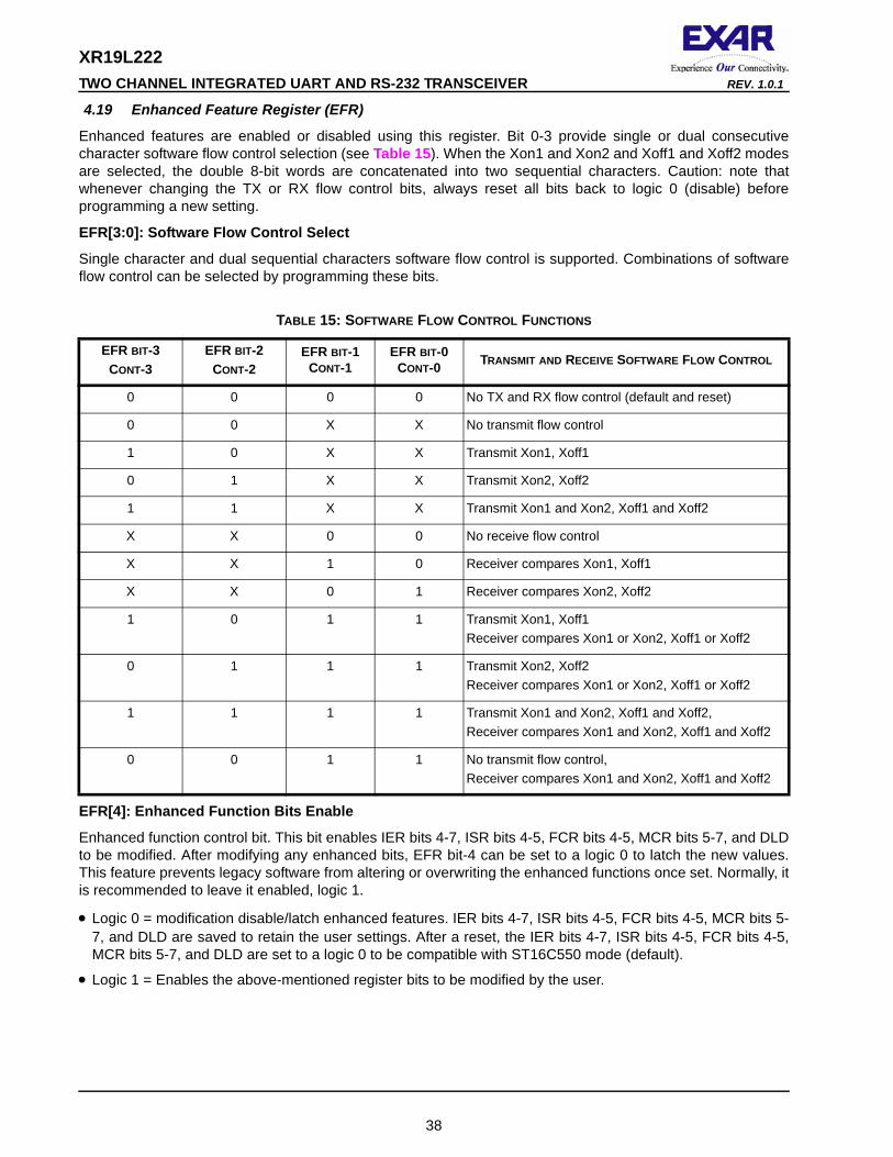
XR19L222 TWO CHANNEL INTEGRATED UART AND RS-232 TRANSCEIVER REV. 1.0.1
4.19 Enhanced Feature Register (EFR)
Enhanced features are enabled or disabled using this register. Bit 0-3 provide single or dual consecutive character software flow control selection (see Table 15). When the Xon1 and Xon2 and Xoff1 and Xoff2 modes are selected, the double 8-bit words are concatenated into two sequential characters. Caution: note that whenever changing the TX or RX flow control bits, always reset all bits back to logic 0 (disable) before programming a new setting.
EFR[3:0]: Software Flow Control Select
Single character and dual sequential characters software flow control is supported. Combinations of software flow control can be selected by programming these bits.
EFR[4]: Enhanced Function Bits Enable
Enhanced function control bit. This bit enables IER bits 4-7, ISR bits 4-5, FCR bits 4-5, MCR bits 5-7, and DLD to be modified. After modifying any enhanced bits, EFR bit-4 can be set to a logic 0 to latch the new values. This feature prevents legacy software from altering or overwriting the enhanced functions once set. Normally, it is recommended to leave it enabled, logic 1.
• Logic 0 = modification disable/latch enhanced features. IER bits 4-7, ISR bits 4-5, FCR bits 4-5, MCR bits 5-7, and DLD are saved to retain the user settings. After a reset, the IER bits 4-7, ISR bits 4-5, FCR bits 4-5, MCR bits 5-7, and DLD are set to a logic 0 to be compatible with ST16C550 mode (default).
• Logic 1 = Enables the above-mentioned register bits to be modified by the user.
TABLE 15: SOFTWARE FLOW CONTROL FUNCTIONS
EFR BIT-3 CONT-3
EFR BIT-2 CONT-2
EFR BIT-1 CONT-1
EFR BIT-0 CONT-0 TRANSMIT AND RECEIVE SOFTWARE FLOW CONTROL
0 0 0 0 No TX and RX flow control (default and reset)
0 0 X X No transmit flow control
1 0 X X Transmit Xon1, Xoff1
0 1 X X Transmit Xon2, Xoff2
1 1 X X Transmit Xon1 and Xon2, Xoff1 and Xoff2
X X 0 0 No receive flow control
X X 1 0 Receiver compares Xon1, Xoff1
X X 0 1 Receiver compares Xon2, Xoff2
1 0 1 1 Transmit Xon1, Xoff1Receiver compares Xon1 or Xon2, Xoff1 or Xoff2
0 1 1 1 Transmit Xon2, Xoff2Receiver compares Xon1 or Xon2, Xoff1 or Xoff2
1 1 1 1 Transmit Xon1 and Xon2, Xoff1 and Xoff2,Receiver compares Xon1 and Xon2, Xoff1 and Xoff2
0 0 1 1 No transmit flow control,Receiver compares Xon1 and Xon2, Xoff1 and Xoff2
38
XR19L222REV. 1.0.1 TWO CHANNEL INTEGRATED UART AND RS-232 TRANSCEIVER
EFR[5]: Special Character Detect Enable
• Logic 0 = Special Character Detect Disabled (default).
• Logic 1 = Special Character Detect Enabled. The UART compares each incoming receive character with data in Xoff-2 register. If a match exists, the receive data will be transferred to FIFO and ISR bit-4 will be set to indicate detection of the special character. Bit-0 corresponds with the LSB bit of the receive character. If flow control is set for comparing Xon1, Xoff1 (EFR [1:0]= ‘10’) then flow control and special character work normally. However, if flow control is set for comparing Xon2, Xoff2 (EFR[1:0]= ‘01’) then flow control works normally, but Xoff2 will not go to the FIFO, and will generate an Xoff interrupt and a special character interrupt, if enabled via IER bit-5.
EFR[6]: Auto RTS Flow Control Enable
RTS# output may be used for hardware flow control by setting EFR bit-6 to logic 1. When Auto RTS is selected, an interrupt will be generated when the receive FIFO is filled to the programmed trigger level and RTS de-asserts HIGH at the next upper trigger level or hysteresis level. RTS# will return LOW when FIFO data falls below the next lower trigger level. The RTS# output must be asserted (LOW) before the auto RTS can take effect. RTS# pin will function as a general purpose output when hardware flow control is disabled.
• Logic 0 = Automatic RTS flow control is disabled (default).
• Logic 1 = Enable Automatic RTS flow control.
EFR[7]: Auto CTS Flow Control Enable
Automatic CTS Flow Control.
• Logic 0 = Automatic CTS flow control is disabled (default).
• Logic 1 = Enable Automatic CTS flow control. Data transmission stops when CTS# input de-asserts HIGH. Data transmission resumes when CTS# returns LOW.
4.19.1 Software Flow Control Registers (XOFF1, XOFF2, XON1, XON2) - Read/Write
These registers are used as the programmable software flow control characters xoff1, xoff2, xon1, and xon2. For more details, see Table 7.
39
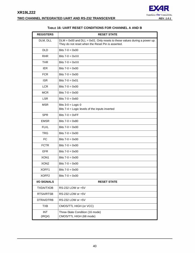
XR19L222 TWO CHANNEL INTEGRATED UART AND RS-232 TRANSCEIVER REV. 1.0.1
TABLE 16: UART RESET CONDITIONS FOR CHANNEL A AND B
REGISTERS RESET STATE
DLM, DLL DLM = 0x00 and DLL = 0x01. Only resets to these values during a power up. They do not reset when the Reset Pin is asserted.
DLD Bits 7-0 = 0x00
RHR Bits 7-0 = 0xXX
THR Bits 7-0 = 0xXX
IER Bits 7-0 = 0x00
FCR Bits 7-0 = 0x00
ISR Bits 7-0 = 0x01
LCR Bits 7-0 = 0x00
MCR Bits 7-0 = 0x00
LSR Bits 7-0 = 0x60
MSR Bits 3-0 = Logic 0 Bits 7-4 = Logic levels of the inputs inverted
SPR Bits 7-0 = 0xFF
EMSR Bits 7-0 = 0x80
FLVL Bits 7-0 = 0x00
TRG Bits 7-0 = 0x00
FC Bits 7-0 = 0x00
FCTR Bits 7-0 = 0x00
EFR Bits 7-0 = 0x00
XON1 Bits 7-0 = 0x00
XON2 Bits 7-0 = 0x00
XOFF1 Bits 7-0 = 0x00
XOFF2 Bits 7-0 = 0x00
I/O SIGNALS RESET STATE
TXDA/TXDB RS-232 LOW or +5V
RTSA/RTSB RS-232 LOW or +5V
DTRA/DTRB RS-232 LOW or +5V
TXB CMOS/TTL HIGH (or VCC)
INT(IRQ#)
Three-State Condition (16 mode)CMOS/TTL HIGH (68 mode)
40
XR19L222REV. 1.0.1 TWO CHANNEL INTEGRATED UART AND RS-232 TRANSCEIVER
ABSOLUTE MAXIMUM RATINGSPower Supply Range 5.5 Volts
Voltage at Any Pin GND-0.3 V to 5.5 V
Operating Temperature -40o to +85oC
Storage Temperature -65o to +150oC
Package Dissipation 500 mW
TYPICAL PACKAGE THERMAL RESISTANCE DATA (MARGIN OF ERROR: ± 15%)
Thermal Resistance (64-QFN) theta-ja = 40oC/W, theta-jc = 13oC/W
41
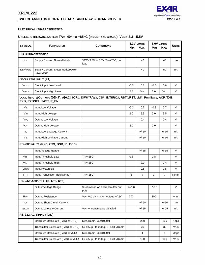
XR19L222 TWO CHANNEL INTEGRATED UART AND RS-232 TRANSCEIVER REV. 1.0.1
ELECTRICAL CHARACTERISTICS
UNLESS OTHERWISE NOTED: TA= -40O TO +85OC (INDUSTRIAL GRADE), VCC= 3.3 - 5.5V
SYMBOL PARAMETER CONDITIONS3.3V LIMITSMIN MAX
5.0V LIMITSMIN MAX
UNITS
DC CHARACTERISTICS
ICC Supply Current, Normal Mode VCC=3.3V to 5.5V, TA=+25C, no load
40 45 mA
ISLP/IPWS Supply Current, Sleep Mode/Power-Save Mode
40 50 uA
OSCILLATOR INPUT (X1)
VILCK Clock Input Low Level -0.3 0.6 -0.5 0.6 V
VIHCK Clock Input High Level 2.4 VCC 3.0 VCC V
LOGIC INPUTS/OUTPUTS (D[0:7], A[0:2], IOR#, IOW#/R/W#, CS#, INT/IRQ#, RST#/RST, I/M#, PWRSAVE, ACP, TXB, RXB, RXBSEL, FAST, R_EN
VIL Input Low Voltage -0.3 0.7 -0.3 0.7 V
VIH Input High Voltage 2.0 5.5 2.0 5.5 V
VOL Output Low Voltage 0.4 0.4 V
VOH Output High Voltage 2.0 2.0 V
IIL Input Low Leakage Current +/-10 +/-10 uA
IHL Input High Leakage Current +/-10 +/-10 uA
RS-232 INPUTS (RXD, CTS, DSR, RI, DCD)
Input Voltage Range +/-15 +/-15 V
VIHR Input Threshold Low TA=+25C 0.6 0.8 V
VILR Input Threshold High TA=+25C 2.0 2.4 V
VHYS Input Hysteresis 0.5 0.5 V
RTR Input Transmition Resistance TA=+25C 3 7 3 7 Kohm
RS-232 OUTPUTS (TXD, RTS, DTR)
Output Voltage Range 3Kohm load on all transmitter out-puts
+/-5.0 +/-5.0 V
ROR Output Resistance Vcc=0V, transmitter output=+/-2V 300 300 ohm
IOS Output Short-Circuit Current +/-60 +/-60 mA
ILKGR Output Leakage Current Vcc=0, transmitters disabled +/-25 +/-25 uA
RS-232 AC TIMING (TXD)
Maximum Data Rate (FAST = GND) RL=3Kohm, CL=1000pF 250 250 Kbps
Transmitter Slew Rate (FAST = GND) CL = 50pF to 2500pF, RL=3-7Kohm 30 30 V/us
Maximum Data Rate (FAST = VCC) RL=3Kohm, CL=1000pF 1 1 Mbps
Transmitter Slew Rate (FAST = VCC) CL = 50pF to 2500pF, RL=3-7Kohm 100 100 V/us
42
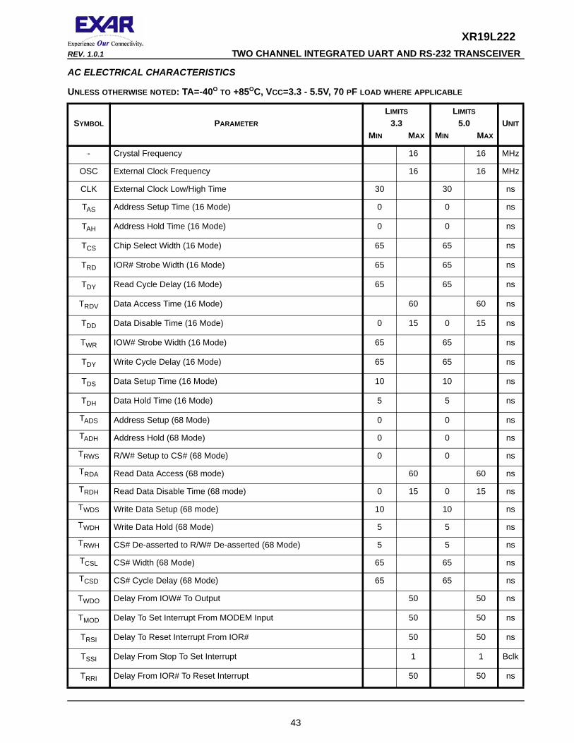
XR19L222REV. 1.0.1 TWO CHANNEL INTEGRATED UART AND RS-232 TRANSCEIVER
AC ELECTRICAL CHARACTERISTICS
UNLESS OTHERWISE NOTED: TA=-40O TO +85OC, VCC=3.3 - 5.5V, 70 PF LOAD WHERE APPLICABLE
SYMBOL PARAMETER
LIMITS
3.3MIN MAX
LIMITS
5.0MIN MAX
UNIT
- Crystal Frequency 16 16 MHz
OSC External Clock Frequency 16 16 MHz
CLK External Clock Low/High Time 30 30 ns
TAS Address Setup Time (16 Mode) 0 0 ns
TAH Address Hold Time (16 Mode) 0 0 ns
TCS Chip Select Width (16 Mode) 65 65 ns
TRD IOR# Strobe Width (16 Mode) 65 65 ns
TDY Read Cycle Delay (16 Mode) 65 65 ns
TRDV Data Access Time (16 Mode) 60 60 ns
TDD Data Disable Time (16 Mode) 0 15 0 15 ns
TWR IOW# Strobe Width (16 Mode) 65 65 ns
TDY Write Cycle Delay (16 Mode) 65 65 ns
TDS Data Setup Time (16 Mode) 10 10 ns
TDH Data Hold Time (16 Mode) 5 5 ns
TADS Address Setup (68 Mode) 0 0 ns
TADH Address Hold (68 Mode) 0 0 ns
TRWS R/W# Setup to CS# (68 Mode) 0 0 ns
TRDA Read Data Access (68 mode) 60 60 ns
TRDH Read Data Disable Time (68 mode) 0 15 0 15 ns
TWDS Write Data Setup (68 mode) 10 10 ns
TWDH Write Data Hold (68 Mode) 5 5 ns
TRWH CS# De-asserted to R/W# De-asserted (68 Mode) 5 5 ns
TCSL CS# Width (68 Mode) 65 65 ns
TCSD CS# Cycle Delay (68 Mode) 65 65 ns
TWDO Delay From IOW# To Output 50 50 ns
TMOD Delay To Set Interrupt From MODEM Input 50 50 ns
TRSI Delay To Reset Interrupt From IOR# 50 50 ns
TSSI Delay From Stop To Set Interrupt 1 1 Bclk
TRRI Delay From IOR# To Reset Interrupt 50 50 ns
43
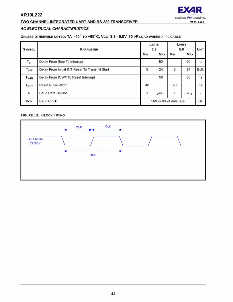
XR19L222 TWO CHANNEL INTEGRATED UART AND RS-232 TRANSCEIVER REV. 1.0.1
TSI Delay From Stop To Interrupt 50 50 ns
TINT Delay From Initial INT Reset To Transmit Start 8 24 8 24 Bclk
TWRI Delay From IOW# To Reset Interrupt 50 50 ns
TRST Reset Pulse Width 40 40 ns
N Baud Rate Divisor 1 216-1 1 216-1 -
Bclk Baud Clock 16X or 8X of data rate Hz
FIGURE 13. CLOCK TIMING
AC ELECTRICAL CHARACTERISTICS
UNLESS OTHERWISE NOTED: TA=-40O TO +85OC, VCC=3.3 - 5.5V, 70 PF LOAD WHERE APPLICABLE
SYMBOL PARAMETER
LIMITS
3.3MIN MAX
LIMITS
5.0MIN MAX
UNIT
OSC
CLKCLK
EXTERNALCLOCK
44
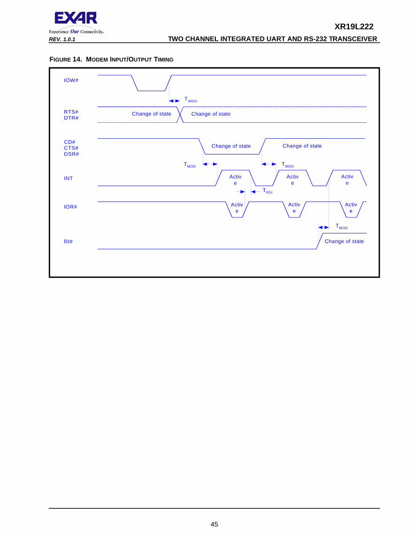
XR19L222REV. 1.0.1 TWO CHANNEL INTEGRATED UART AND RS-232 TRANSCEIVER
FIGURE 14. MODEM INPUT/OUTPUT TIMING
IOW#
RTS#DTR#
CD#CTS#DSR#
INT
IOR#
RI#
TWDO
TMOD TMOD
TRSI
TMOD
Active
Change of state Change of state
Active
Active
Active
Change of state Change of state
Change of state
Active
Active
45
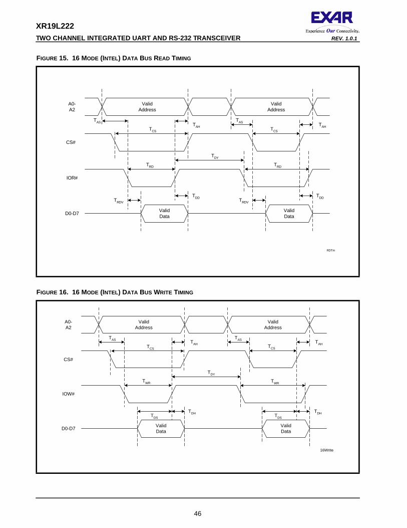
XR19L222 TWO CHANNEL INTEGRATED UART AND RS-232 TRANSCEIVER REV. 1.0.1
FIGURE 15. 16 MODE (INTEL) DATA BUS READ TIMING
FIGURE 16. 16 MODE (INTEL) DATA BUS WRITE TIMING
TAS
TDD
TAH
TRD
TRDV
TDY
TDDTRDV
TAH
TAS
TCS
ValidAddress
ValidAddress
ValidData
ValidData
A0-A2
CS#
IOR#
D0-D7
RDTm
TCS
TRD
16Write
TAS
TDH
TAH
TWR
TDS
TDY
TDHTDS
TAH
TAS
TCS
ValidAddress
ValidAddress
ValidData
ValidData
A0-A2
CS#
IOW#
D0-D7
TCS
TWR
46
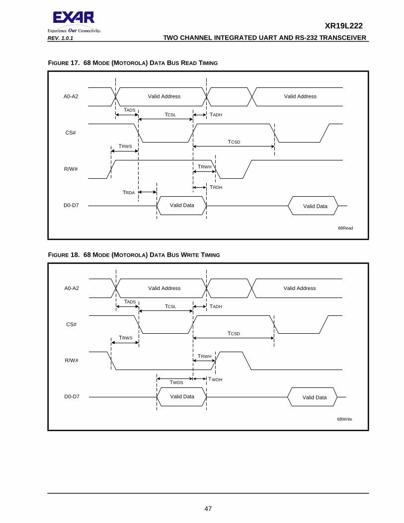
XR19L222REV. 1.0.1 TWO CHANNEL INTEGRATED UART AND RS-232 TRANSCEIVER
FIGURE 17. 68 MODE (MOTOROLA) DATA BUS READ TIMING
FIGURE 18. 68 MODE (MOTOROLA) DATA BUS WRITE TIMING
68Read
TADS
TRDH
TADHTCSL
TRDA
TCSDTRWS
Valid Address Valid Address
Valid Data
A0-A2
CS#
R/W#
D0-D7
TRWH
Valid Data
68Write
TADSTADHTCSL
TWDS
TCSDTRWS
Valid Address Valid Address
Valid Data
A0-A2
CS#
R/W#
D0-D7
TRWH
Valid Data
TWDH
47
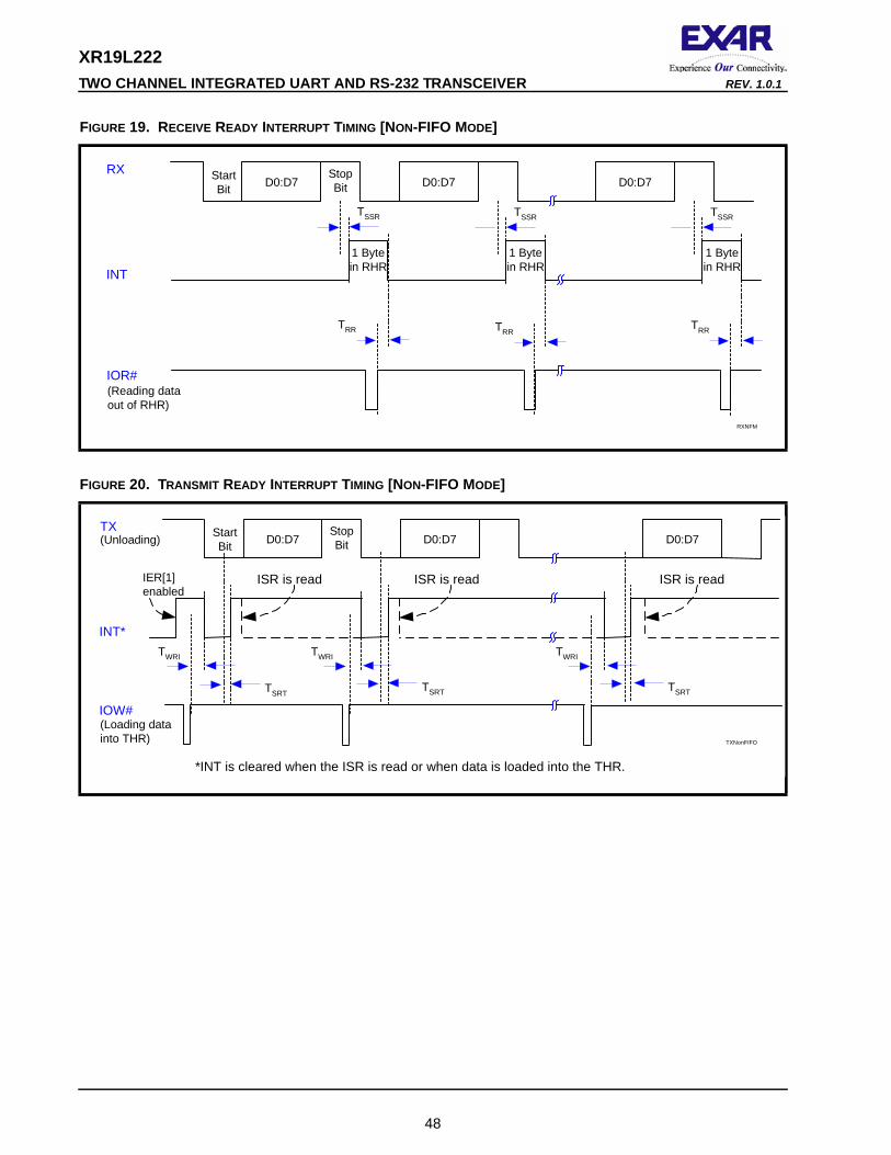
XR19L222 TWO CHANNEL INTEGRATED UART AND RS-232 TRANSCEIVER REV. 1.0.1
FIGURE 19. RECEIVE READY INTERRUPT TIMING [NON-FIFO MODE]
FIGURE 20. TRANSMIT READY INTERRUPT TIMING [NON-FIFO MODE]
RX
INT
D0:D7StartBit D0:D7
StopBit D0:D7
1 Bytein RHR
1 Bytein RHR
1 Bytein RHR
RXNFM
TSSR TSSR TSSR
IOR#
TRR TRRTRR
(Reading dataout of RHR)
TX
INT*
D0:D7StartBit D0:D7
StopBit D0:D7
TXNonFIFO
TWRI TWRI TWRI
TSRT TSRT TSRT
*INT is cleared when the ISR is read or when data is loaded into the THR.
ISR is read ISR is readISR is read
(Unloading)
IER[1]enabled
IOW#(Loading datainto THR)
48
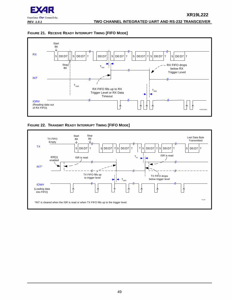
XR19L222REV. 1.0.1 TWO CHANNEL INTEGRATED UART AND RS-232 TRANSCEIVER
FIGURE 21. RECEIVE READY INTERRUPT TIMING [FIFO MODE]
FIGURE 22. TRANSMIT READY INTERRUPT TIMING [FIFO MODE]
RX
INT
D0:D7S
TSSR
RXINTDMA#
RX FIFO fills up to RXTrigger Level or RX Data
Timeout
RX FIFO dropsbelow RX
Trigger Level
D0:D7S D0:D7T D0:D7S D0:D7ST D0:D7ST T D0:D7S T
StartBit
StopBit TSSI
IOR#
TRRI
(Reading data outof RX FIFO)
TX
INT*
TX INT
D0:D7S D0:D7T D0:D7S D0:D7ST D0:D7ST T D0:D7S T
StartBit
StopBit
TWRI
Last Data ByteTransmitted
TX FIFO fills upto trigger level TX FIFO drops
below trigger level
TX FIFOEmpty
TTS
TSIISR is readIER[1]enabled
ISR is read
IOW#(Loading data
into FIFO)
*INT is cleared when the ISR is read or when TX FIFO fills up to the trigger level.
49
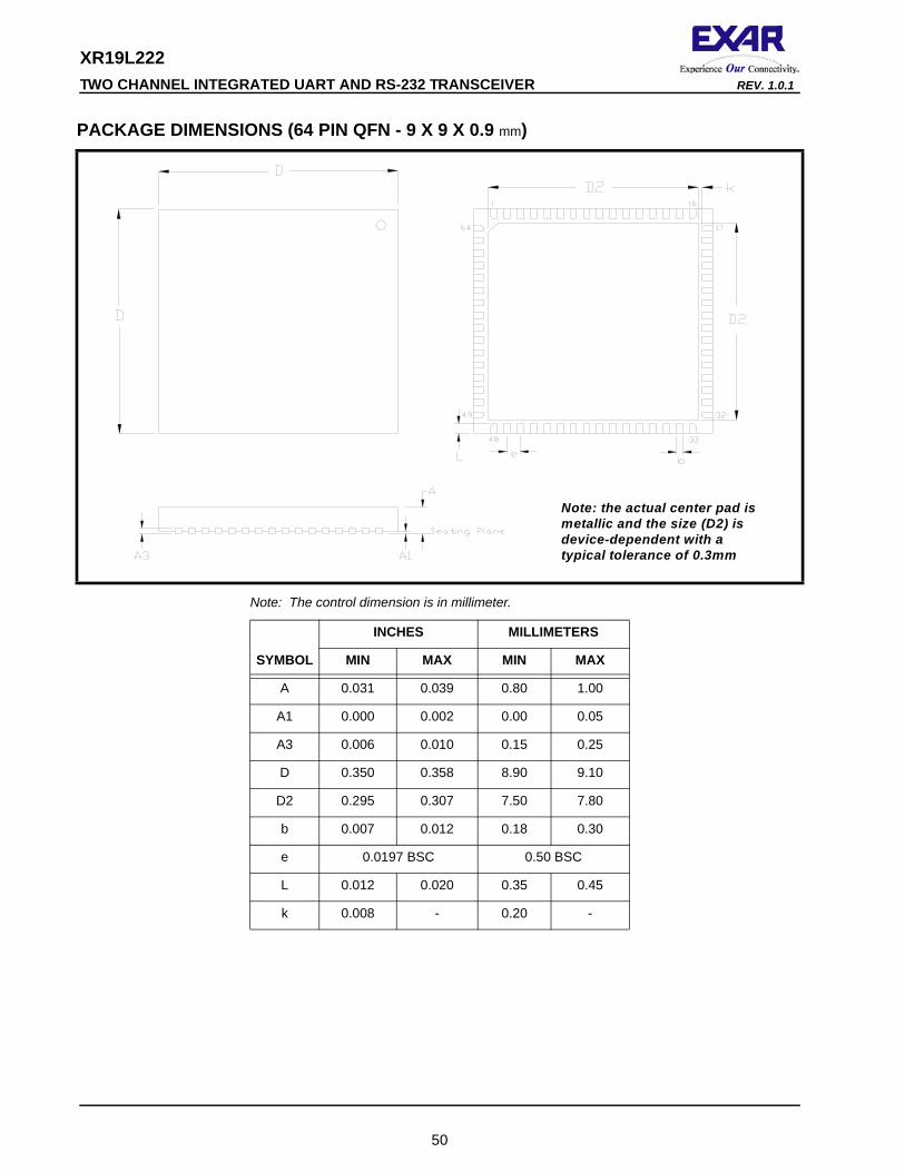
XR19L222 TWO CHANNEL INTEGRATED UART AND RS-232 TRANSCEIVER REV. 1.0.1
PACKAGE DIMENSIONS (64 PIN QFN - 9 X 9 X 0.9 mm)
Note: The control dimension is in millimeter.
INCHES MILLIMETERS
SYMBOL MIN MAX MIN MAX
A 0.031 0.039 0.80 1.00
A1 0.000 0.002 0.00 0.05
A3 0.006 0.010 0.15 0.25
D 0.350 0.358 8.90 9.10
D2 0.295 0.307 7.50 7.80
b 0.007 0.012 0.18 0.30
e 0.0197 BSC 0.50 BSC
L 0.012 0.020 0.35 0.45
k 0.008 - 0.20 -
Note: the actual center pad is metallic and the size (D2) is device-dependent with a typical tolerance of 0.3mm
50
XR19L222REV. 1.0.1 TWO CHANNEL INTEGRATED UART AND RS-232 TRANSCEIVER
REVISION HISTORY
DATE REVISION DESCRIPTION
June 2006 P1.0.0 Preliminary Datasheet
October 2006 P1.0.1 Updated Package Dimensions
January 2007 P1.0.2 Updated EIA/TIA-232-F compliant voltage range to +3.3V to +5.5V.
May 2007 1.0.0 Final Datasheet. Updated DC Electrical Characteristics. Updated QFN drawing.
July 2007 1.0.1 Corrected R_EN pin description.
51
NOTICE
EXAR Corporation reserves the right to make changes to the products contained in this publication in order to improve design, performance or reliability. EXAR Corporation assumes no responsibility for the use of any circuits described herein, conveys no license under any patent or other right, and makes no representation that the circuits are free of patent infringement. Charts and schedules contained here in are only for illustration purposes and may vary depending upon a user’s specific application. While the information in this publication has been carefully checked; no responsibility, however, is assumed for inaccuracies.
EXAR Corporation does not recommend the use of any of its products in life support applications where the failure or malfunction of the product can reasonably be expected to cause failure of the life support system or to significantly affect its safety or effectiveness. Products are not authorized for use in such applications unless EXAR Corporation receives, in writing, assurances to its satisfaction that: (a) the risk of injury or damage has been minimized; (b) the user assumes all such risks; (c) potential liability of EXAR Corporation is adequately protected under the circumstances.
Copyright 2007 EXAR Corporation
Datasheet July 2007.
Send your UART technical inquiry with technical details to hotline: [email protected].
Reproduction, in part or whole, without the prior written consent of EXAR Corporation is prohibited.
XR19L222REV. 1.0.1 TWO CHANNEL INTEGRATED UART AND RS-232 TRANSCEIVER
TABLE OF CONTENTS
GENERAL DESCRIPTION................................................................................................ 1APPLICATIONS .............................................................................................................................................. 1FEATURES.................................................................................................................................................... 1
FIGURE 1. BLOCK DIAGRAM ............................................................................................................................................................. 1FIGURE 2. PIN OUT OF THE DEVICE.................................................................................................................................................. 2
ORDERING INFORMATION .............................................................................................................................. 2PIN DESCRIPTIONS ....................................................................................................... 31.0 PRODUCT DESCRIPTION ...................................................................................................................... 72.0 FUNCTIONAL DESCRIPTIONS .............................................................................................................. 8
2.1 CPU INTERFACE ................................................................................................................................................ 8FIGURE 3. XR19L222 TYPICAL INTEL/MOTOROLA DATA BUS INTERCONNECTIONS ............................................................................. 8
2.2 5-VOLT TOLERANT INPUTS.............................................................................................................................. 92.3 DEVICE HARDWARE RESET............................................................................................................................. 92.4 DEVICE IDENTIFICATION AND REVISION ....................................................................................................... 92.5 CHANNEL A AND B SELECTION ...................................................................................................................... 9
TABLE 1: CHANNEL A AND B SELECT IN 16 MODE ............................................................................................................................ 9TABLE 2: CHANNEL A AND B SELECT IN 68 MODE ............................................................................................................................ 9
2.6 CHANNEL A AND B INTERNAL REGISTERS................................................................................................... 92.7 DMA MODE ....................................................................................................................................................... 102.8 INT (IRQ#) OUTPUT .......................................................................................................................................... 10
TABLE 3: INT (IRQ#) PIN OPERATION FOR TRANSMITTER ............................................................................................................... 10TABLE 4: INT (IRQ#) PIN OPERATION FOR RECEIVER .................................................................................................................... 10
2.9 CRYSTAL OR EXTERNAL CLOCK INPUT ...................................................................................................... 10FIGURE 4. TYPICAL CRYSTAL CONNECTIONS .................................................................................................................................. 11
2.10 PROGRAMMABLE BAUD RATE GENERATOR WITH FRACTIONAL DIVISOR ......................................... 11FIGURE 5. BAUD RATE GENERATOR ............................................................................................................................................... 12TABLE 5: TYPICAL DATA RATES WITH A 24 MHZ CRYSTAL OR EXTERNAL CLOCK AT 16X SAMPLING ................................................... 13
2.11 TRANSMITTER................................................................................................................................................ 142.11.1 TRANSMIT HOLDING REGISTER (THR) - WRITE ONLY......................................................................................... 142.11.2 TRANSMITTER OPERATION IN NON-FIFO MODE .................................................................................................. 14
FIGURE 6. XR19L222 TRANSMITTER AND RECEIVER ...................................................................................................................... 14FIGURE 7. TRANSMITTER OPERATION IN NON-FIFO MODE .............................................................................................................. 15
2.11.3 TRANSMITTER OPERATION IN FIFO MODE ........................................................................................................... 15FIGURE 8. TRANSMITTER OPERATION IN FIFO AND FLOW CONTROL MODE ..................................................................................... 15
2.12 RECEIVER ....................................................................................................................................................... 152.12.1 RECEIVE HOLDING REGISTER (RHR) - READ-ONLY ............................................................................................ 162.12.2 SELECTABLE INPUT TO RX OF CHANNEL B......................................................................................................... 16
FIGURE 9. RECEIVER OPERATION IN NON-FIFO MODE.................................................................................................................... 16FIGURE 10. RECEIVER OPERATION IN FIFO AND AUTO RTS FLOW CONTROL MODE ....................................................................... 17
2.13 AUTO RTS (HARDWARE) FLOW CONTROL............................................................................................... 172.14 AUTO RTS HYSTERESIS .............................................................................................................................. 172.15 AUTO CTS FLOW CONTROL........................................................................................................................ 18
FIGURE 11. AUTO RTS AND CTS FLOW CONTROL OPERATION....................................................................................................... 182.16 AUTO XON/XOFF (SOFTWARE) FLOW CONTROL..................................................................................... 19
TABLE 6: AUTO XON/XOFF (SOFTWARE) FLOW CONTROL ............................................................................................................... 192.17 SPECIAL CHARACTER DETECT.................................................................................................................. 192.18 SLEEP MODES AND POWER-SAVE FEATURE WITH WAKE-UP INTERRUPT ........................................ 20
2.18.1 PARTIAL SLEEP MODE............................................................................................................................................. 202.18.1.1 UART IN SLEEP MODE, RS-232 TRANSCEIVER ACTIVE......................................................................................... 202.18.1.2 UART ACTIVE, CHARGE PUMP OF RS-232 TRANSCEIVER SHUT DOWN.................................................................. 21
2.18.2 FULL SLEEP MODE ................................................................................................................................................... 212.18.3 POWER-SAVE FEATURE .......................................................................................................................................... 21
2.19 INFRARED MODE (UART CHANNEL B ONLY)............................................................................................. 22FIGURE 12. INTERNAL LOOP BACK ................................................................................................................................................. 22
3.0 UART INTERNAL REGISTERS............................................................................................................. 23TABLE 7: UART INTERNAL REGISTERS ........................................................................................................................................... 23TABLE 8: INTERNAL REGISTERS DESCRIPTION. SHADED BITS ARE ENABLED WHEN EFR BIT-4=1 .................................................... 24
4.0 INTERNAL REGISTER DESCRIPTIONS .............................................................................................. 254.1 RECEIVE HOLDING REGISTER (RHR) - READ- ONLY.................................................................................. 25
I
XR19L222 TWO CHANNEL INTEGRATED UART AND RS-232 TRANSCEIVER REV. 1.0.1
4.2 TRANSMIT HOLDING REGISTER (THR) - WRITE-ONLY ............................................................................... 254.3 INTERRUPT ENABLE REGISTER (IER) - READ/WRITE................................................................................. 25
4.3.1 IER VERSUS RECEIVE FIFO INTERRUPT MODE OPERATION ............................................................................... 264.3.2 IER VERSUS RECEIVE/TRANSMIT FIFO POLLED MODE OPERATION.................................................................. 26
4.4 INTERRUPT STATUS REGISTER (ISR) - READ-ONLY .................................................................................. 274.4.1 INTERRUPT GENERATION: ........................................................................................................................................ 274.4.2 INTERRUPT CLEARING: ............................................................................................................................................. 28
TABLE 9: INTERRUPT SOURCE AND PRIORITY LEVEL ....................................................................................................................... 284.5 FIFO CONTROL REGISTER (FCR) - WRITE-ONLY......................................................................................... 29
TABLE 10: TRANSMIT AND RECEIVE FIFO TRIGGER TABLE AND LEVEL SELECTION .......................................................................... 304.6 LINE CONTROL REGISTER (LCR) - READ/WRITE......................................................................................... 30
TABLE 11: PARITY SELECTION ........................................................................................................................................................ 314.7 MODEM CONTROL REGISTER (MCR) OR GENERAL PURPOSE OUTPUTS CONTROL - READ/WRITE.. 324.8 LINE STATUS REGISTER (LSR) - READ ONLY.............................................................................................. 334.9 MODEM STATUS REGISTER (MSR) - READ ONLY ....................................................................................... 344.10 SCRATCH PAD REGISTER (SPR) - READ/WRITE ....................................................................................... 354.11 ENHANCED MODE SELECT REGISTER (EMSR) ......................................................................................... 35
TABLE 12: SCRATCHPAD SWAP SELECTION .................................................................................................................................... 35TABLE 13: AUTO RTS HYSTERESIS ................................................................................................................................................ 35
4.12 FIFO LEVEL REGISTER (FLVL) - READ-ONLY............................................................................................. 364.13 BAUD RATE GENERATOR REGISTERS (DLL, DLM AND DLD) - READ/WRITE ....................................... 364.14 DEVICE IDENTIFICATION REGISTER (DVID) - READ ONLY....................................................................... 364.15 DEVICE REVISION REGISTER (DREV) - READ ONLY................................................................................. 364.16 TRIGGER LEVEL REGISTER (TRG) - WRITE-ONLY .................................................................................... 364.17 RX/TX FIFO LEVEL COUNT REGISTER (FC) - READ-ONLY ....................................................................... 374.18 FEATURE CONTROL REGISTER (FCTR) - READ/WRITE........................................................................... 37
TABLE 14: TRIGGER TABLE SELECT ................................................................................................................................................ 374.19 ENHANCED FEATURE REGISTER (EFR) ..................................................................................................... 38
TABLE 15: SOFTWARE FLOW CONTROL FUNCTIONS ........................................................................................................................ 384.19.1 SOFTWARE FLOW CONTROL REGISTERS (XOFF1, XOFF2, XON1, XON2) - READ/WRITE .............................. 39
TABLE 16: UART RESET CONDITIONS FOR CHANNEL A AND B ............................................................................................ 40ABSOLUTE MAXIMUM RATINGS.................................................................................. 41TYPICAL PACKAGE THERMAL RESISTANCE DATA (MARGIN OF ERROR: ± 15%) 41
AC ELECTRICAL CHARACTERISTICS ............................................................................................................. 43Unless otherwise noted: TA=-40o to +85oC, Vcc=3.3 - 5.5V, 70 pF load where applicable .................................... 43
FIGURE 13. CLOCK TIMING............................................................................................................................................................. 44FIGURE 14. MODEM INPUT/OUTPUT TIMING .................................................................................................................................... 45FIGURE 15. 16 MODE (INTEL) DATA BUS READ TIMING ................................................................................................................... 46FIGURE 16. 16 MODE (INTEL) DATA BUS WRITE TIMING.................................................................................................................. 46FIGURE 17. 68 MODE (MOTOROLA) DATA BUS READ TIMING .......................................................................................................... 47FIGURE 18. 68 MODE (MOTOROLA) DATA BUS WRITE TIMING......................................................................................................... 47FIGURE 19. RECEIVE READY INTERRUPT TIMING [NON-FIFO MODE] ............................................................................................... 48FIGURE 20. TRANSMIT READY INTERRUPT TIMING [NON-FIFO MODE] ............................................................................................. 48FIGURE 21. RECEIVE READY INTERRUPT TIMING [FIFO MODE] ....................................................................................................... 49FIGURE 22. TRANSMIT READY INTERRUPT TIMING [FIFO MODE] ..................................................................................................... 49
PACKAGE DIMENSIONS (64 PIN QFN - 9 X 9 X 0.9 mm) .............................................. 50REVISION HISTORY...................................................................................................................................... 51
II