Embed Size (px)
Citation preview
1
Tunable Sensors for Process-Aware Voltage Scaling
Tuck-Boon Chan‡ and Andrew B. Kahng†‡
CSE† and ECE‡ Departments, UCSD
[email protected], [email protected]://vlsicad.ucsd.edu

2
Outline• Intro: Adaptive Voltage Scaling (AVS)• Overview of Proposed Method• Voltage Scaling Properties• Designing the Circuit• Results

3
Adaptive Voltage Scaling
• Circuits are designed to guardband for performance variation
• There is margin for typical chips• Adaptive voltage scaling (AVS) adjusts
voltage to reduce power
Voltage
a typical chip
worst-case scenario(e.g, due to process variation)targetf
Maximum frequency
margin
reduce voltage meet performance with less power
Vnominal

4
Taxonomy of AVS Techniques
Open-Loop AVS
Closed-Loop AVSP
ow
er
Freq. & Vdd LUT
Post-silicon characterization
AVS Pre-characterize LUT [Martin02]
Process-aware AVSPost-silicon characterization [Tschanz03]
Generic monitor
Design dependent replica
In-situmonitor
Process and temperature-aware AVS Generic on-chip monitor [Burd00]Design-dependent monitor [Elgebaly07, Drake08, Chan12]
In-situ performance monitor Measure actual critical paths [Hartman06, Fick10]
Error Detection System
Error detection and correction system Vdd scaling until error occurs [Das06,Tschanz10]
Error Tolerance
AVS
approachesAVS classes

5
Motivation for Closed-Loop AVS
• Closed-loop AVS saves up to 62% dynamic power
[Hartman06]

6
Classes of Closed-Loop AVS
• Critical path may be difficult to identify (IP from 3rd party)
• Calibrating monitors at multiple modes/voltages requires long test time
Closed-Loop AVS
Design-dependent replica
In-situmonitor
Generic monitor
• Does not capture design-specific performance variation
This work: Tunable monitor for closed-loop AVS• Can be applied as a generic monitor• Or tuned to capture design-specific performance

7
Outline• Intro: Adaptive Voltage Scaling (AVS)• Overview of Proposed Method• Voltage Scaling Properties• Designing the Circuit• Results

8
Voltage Scaling Key Concepts
• Process distance: process-induced frequency shift relative to target frequency
• Scaling rate: frequency shift (f) per unit voltage difference (V)
• Vmin= Minimum Vdd to meet target frequency• Calculated from process distance and scaling rate
Voltage
SS
k
targetf
nomV)(kVmin_path
Process distance
Max. freq.
Scaling rate =V
f

Monitor Design Concept• Use Vmin of ring-oscillator (RO) as a reference
• Design ROs with worst-case voltage scaling properties an arbitrary circuit will meet target frequency at Vmin_ro
Vmin of ROs Max. Vmin of paths 9
>
V
RO
Critical paths
targetf
Freq.
Process corner A
RO
V
Critical paths
targetf
Freq.
Process corner B
Max.

10
Proposed Method: Tunable Monitor
• Our focus is on voltage scaling property analyze worst-case voltage scaling
Store config.Scenario 2: With chips at process corners
• Extract Fmax and Vmin of chips• Tune voltage scaling properties of ROs
so that Vmin_ro > Vmin_chip
• Recover margin with one calibration
Scenario 1: Without circuit information• Configure RO for worst-case Vmin
• Guardband for arbitrary circuits

Problems• Goal: Vmin_ro > Vmin_path • Questions: Given a process
technology, what is the range of the Vmin that is defined by process distance and scaling rate for arbitrary critical paths?
What circuit techniques can “tune” Vmin?
11
V
Vmin of arbitrary critical paths
targetf
freq.
Vmin
Path BPath A
= ?Also, Vmin changes at different process corners
Path C

12
Outline• Intro: Adaptive Voltage Scaling (AVS)• Overview of Proposed Method• Voltage Scaling Properties• Designing the Circuit• Results

13
Vmin Analytical Derivation
fpath = inverse of average delays of NMOS & PMOS
),(),(),(
nompmosnomnmosnom
2
VkDVkDVkf path
rate scaling
distance processnommin VV
),(),(
),(
nomnom
targetnomnom VkfVVkf
fVkfV
pathpath
path
(1)
(2)
Calculate delays with• Elmore delay model• Effective currents of transistors
(3)
Process distance
Scaling rate

14
Vmin Sensitivity
• Vmin is not very sensitive to fanout, interconnect load, etc.
• Empirically, bounds on Vmin determined by NMOS and PMOS
0.2 0.6 1.0 1.4 1.8 2.2 2.6 3.0 3.4 3.80.9700.9800.9901.0001.0101.020
fanout l beta Ron NMOSRon PMOS
Normalized value of circuit parameters
Nor
mal
ized
Vm
in
wire length
Vmin for PMOS only
Vmin for NMOS only

15
Effects of Fanout and Series Resistance
• Fanout has little effect on Vmin
FO1 FO2 FO4 FO80.600.700.800.901.00
SS TT FF SF FS
Fanout
Vm
in (V
)
1 100 200 400 800 16000.600.700.800.901.00
SS TT FF SF FS
Series resistance (ohm)
Vmin
(V)
High series resistance reduces Vmin
But, need long wires

16
Effects of Cell Type
• Cell type affects Vmin
• Maximum Vmin at different corners are determined by different cell types
• Stacking causes cell delay biased to PMOS or NMOS changes device characteristics and Vmin
INVX0
NAND2X0
NAND3X0
NAND4X0
NOR2X0
NOR3X0
NOR4X00.500.600.700.800.901.001.10
SS TT FF SF FS
Cell type
Vmin
(V)

17
Effects of Cell Strength
• Vmin does not increase from X1 to X3• But increases from X0 to X1•X1 to X3 {1,2,3} fingers, same device characteristic•X0 to X1 Both 1 finger but different diffusion area
X0 X1 X2 X30.500.600.700.800.901.001.10
SS TT FF SF
INV. cell strength
Vmin
(V)
X0 X1 X2 X30.500.600.700.800.901.001.10
SS TT FF SF FS
NAND3 cell strength
Vmin
(V)
Cell layout changes device characteristics and Vmin

18
Outline• Intro: Adaptive Voltage Scaling (AVS)• Overview of Proposed Method• Voltage Scaling Properties• Designing the Circuit• Results

19
Design of RO with Tunable Vmin
• Identified two circuit knobs to tune Vmin
• Series resistance• Cell types (INV, NAND, NOR)
• Proposed circuit• ROs with different cell types (worst-case Vmin are determined
by different cells at different process corners)
• Tune Vmin a configurable series resistance at each stage
1 bit 1 bit 1 bit Control pins
High resistance
Low resistance
20
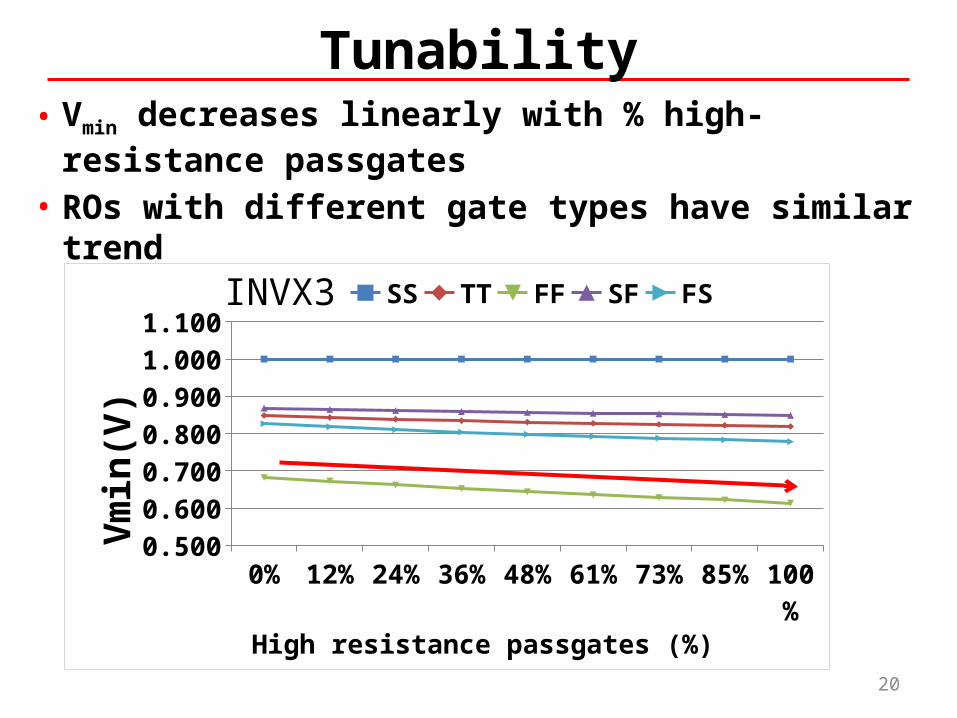
Tunability• Vmin decreases linearly with % high-resistance
passgates• ROs with different gate types have similar trend
INVX3
0% 12% 24% 36% 48% 61% 73% 85% 100%0.5000.6000.7000.8000.9001.0001.100
SS TT FF SF FS
High resistance passgates (%)
Vmin
(V)

21
Outline• Intro: Adaptive Voltage Scaling (AVS)• Overview of Proposed Method• Voltage Scaling Properties• Designing the Circuit• Results

Experiment Methodology
22
• Goal: Validate PVS ROs in simulation• Check Vmin of ROs vs. Vmin of paths• with arbitrary circuits and process variation
• Experiment setup:• 65nm industrial technology• Implement 3 testcases (arbitrary circuits)• Implement 3 tunable ROs (INV, NAND, NOR)
Power (mW) Area (mm2) Freq. targetFPU 4.1 0.015 710TLU 438.0 0.098 507MUL 19.8 0.050 1042

Process Variation Setup• Simulate critical paths and ROs with SPICE
200 Monte Carlo samples (global variation)• 4 variation sources, Gaussian distributions
• Difference between slow and fast corners define +/- 3 sigma values of variation sources
23
Variation sources mean +/- 3 sigmaNMOS Vth 0 30mVPMOS Vth 0 30mVChannel length 0 5nmGate oxide thickness 0 0.06nm

24
Vmin Extraction and Comparison
• Define ftarget of chip and ROs at “slow-slow” process corner nominal voltage = 1.0V
• Vmin_chip = max. Vmin of critical paths of a testcase
• Vmin_est = max. Vmin of 3 ROs
• For each testcase, calculate Vmin_est - Vmin_chip of every Monte Carlo sample
• A chip is safe when Vmin_est - Vmin_chip > 0

Scenario 1: Guardband for Arbitrary Circuit• Vmin_est - Vmin_chip > 0 under
process variation• Similar results for different
testcases• Small difference between
normal and tunable ROs due to series passgates
25
FPU testcase
MUL testcase
TLU testcase

26
Scenario 2: Tune ROs for Margin Reduction• Extract Vmin_chip at different process corners• Configure % high-resistance passgates
Ensures Vmin_est guided by ROs is always safe
kkVkV ),()( min_chipmin_est
})()({ k
kVkV min_chipmin_estmin. :
s.t. : )},,({max)( cikVkVi
min_romin_est

Experiment Result on Tunability
27
Aggressive config. Vmin_est < Vmin_chip Some chips will fail
Optimized config.• Increase % high
resistance passgates• Vmin_est ≈ Vmin_chip
Default config.
• Low resistance passgates
• Guardband for worst-case
• Vmin_est > Vmin_chip
• 13mV margin

Experiment Result on Tunability
28
Aggressive config. Vmin_est < Vmin_chip Some chips will fail
Default config.
• Low resistance passgates
• Guardband for worst-case
• Vmin_est > Vmin_chip
• 13mV margin
Optimized config.• Increase % high
resistance passgates• Vmin_est ≈ Vmin_chip
Benefits of tunability • Recover voltage margin• Compensate for difference between
SPICE model vs. silicon• Recover margin when chip performance
variation is reduced due to improvements in chip manufacturing

29
Summary• Monitor design based on voltage scaling properties • Estimate the worst-case voltage scaling property
across different process corners Does not require information about critical paths Can be used as an IP for arbitrary circuits
• Recover margin if fmax of sample silicon is available• Future works
Proof of concept silicon Account for performance variation due to layout
context

31
Backup Slides

32
Effects of Pass Gates
• Pass gate is equivalent to large resistance• Vmin decreases with fewer parallel pass gates
Vmin decreases

33
Effects of Cell Type and Strength• Key observations: Vmin is affected by cell typesUse NAND, NOR type ROs
• Cell strength changes Vmin Use cells with large Vmin