Embed Size (px)
Citation preview
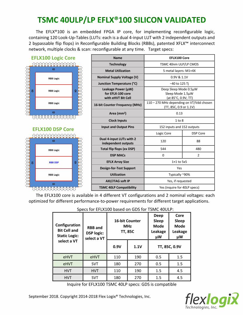
TSMC 40ULP/LP EFLX®100 SILICON VALIDATED
September 2018. Copyright 2014-2018 Flex Logix® Technologies, Inc.
The EFLX®100 is an embedded FPGA IP core, for implementing reconfigurable logic, containing 120 Look-Up-Tables (LUTs: each is a dual 4-input LUT with 2 independent outputs and 2 bypassable flip flops) in Reconfigurable Building Blocks (RBBs), patented XFLX™ interconnect network, multiple clocks & scan: reconfigurable at any time. Target specs:
EFLX100 Logic Core
EFLX100 DSP Core
The EFLX100 core is available in 4 different VT configurations and 2 nominal voltages: each optimized for different performance-to-power requirements for different target applications.
Specs for EFLX100 based on GDS for TSMC 40ULP:
Configuration Bit Cell and Static Logic: select a VT
RBB and DSP logic: select a VT
16-bit Counter MHz
TT, 85C
Deep Sleep Mode
Leakage μW
Core Sleep Mode
Leakage μW
0.9V 1.1V TT, 85C, 0.9V
eHVT eHVT 110 190 0.5 1.5 eHVT SVT 180 270 0.5 1.5 HVT HVT 110 190 1.5 4.5 HVT SVT 180 270 1.5 4.5
Inquire for EFLX100 TSMC 40LP specs: GDS is compatible
Name EFLX100 Core
Technology TSMC 40nm ULP/LP CMOS
Metal Utilization 5 metal layers: M1+4X
Nominal Supply Voltage (V) 0.9V & 1.1V
Junction Temperature (°C) −40 to 125 Tj Leakage Power (μW)
for EFLX-100 core with eHVT Bit Cell
Deep Sleep Mode 0.5μW Sleep Mode 1.5μW (at 85°C, 0.9V, TT)
16-bit Counter Frequency (MHz) 110 – 270 MHz depending on VT/Vdd chosen (TT, 85C, 0.9 or 1.1V)
Area (mm2) 0.13
Clock Inputs 1 to 8
Input and Output Pins 152 inputs and 152 outputs
Logic Core DSP Core Dual 4-input LUTs with 2
independent outputs 120 88
Total flip flops (ex DSP) 544 480
DSP MACs 0 2
EFLX Array Size 1×1 to 5x5
Design-for-Test Support Yes
Utilization Typically ~90%
AXI/JTAG soft IP Yes, if requested
TSMC 40LP Compatibility Yes (inquire for 40LP specs)
RBB DSP
RBB Logic
RBB Logic
IO
IO
IO IO
RBB Logic
RBB Logic
RBB Logic
IO
IO
IO
IO
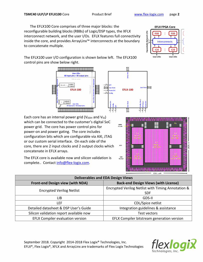
TSMC40 ULP/LP EFLX100 Core Product Brief www.flex-logix.com page 2
September 2018. Copyright 2014-2018 Flex Logix® Technologies, Inc. EFLX®, Flex Logix®, XFLX and ArrayLinx are trademarks of Flex Logix Technologies
The EFLX100 Core comprises of three major blocks: the reconfigurable building blocks (RBBs) of Logic/DSP types, the XFLX interconnect network, and the user I/Os. EFLX features full connectivity inside the core, and provides ArrayLinx™ interconnects at the boundary to concatenate multiple.
The EFLX100 user I/O configuration is shown below left. The EFLX100 control pins are show below right.
Each core has an internal power grid (VDDH and VSS) which can be connected to the customer’s digital SoC power grid. The core has power control pins for power-on and power gating. The core includes configuration bits which are configurable via AXI, JTAG or our custom serial interface. On each side of the core, there are 2 input clocks and 2 output clocks which concatenate in EFLX arrays.
The EFLX core is available now and silicon validation is complete.. Contact [email protected].
EFLX-100
User
Clo
ck
User Clock
User Clock
5
Conf
ig. (
Aux.
)
3
DFT (
Aux.
)
Pow
er C
trl
22
Conf
ig.
DFT
2Po
wer
Ctr
l2
User Clock
6Config.
Power Ctrl
DFT3
EFLX-100~4
38µm
act
ual= 1 output
& 1 inputs
User I/Os: 60 input pins + 60 output pins
User
I/Os
: 16
inpu
t pin
s + 1
6 ou
tput
pin
s
User I/Os:60 input pins + 60 output pins
= 1 outputs & 1 inputsUs
er I/
Os: 1
6 in
put p
ins +
16
outp
ut p
ins ~298 um actual
Deliverables and EDA Design Views Front-end Design view (with NDA) Back-end Design Views (with License)
Encrypted Verilog Netlist Encrypted Verilog Netlist with Timing Annotation & SDF
LIB GDS-II LEF CDL/Spice netlist
Detailed datasheet & DSP User’s Guide Integration guidelines & assistance Silicon validation report available now Test vectors
EFLX Compiler evaluation version EFLX Compiler bitstream generation version
RBBRBB
IOB
煑
煑IOB
Interconnects
Expa
ndab
le N
etw
ork
I/O
s
User I/Os
EFLX FPGA Core
User I/Os