Embed Size (px)
Citation preview
TroubleshootingGuide
Regenerative DC Bus Supply Unit (RGU)
Bulletin 2364F
Allen-Bradley
Important User Information Because of the variety of uses for the products described in this publication those responsible for the application and use of this control equipment must satisfy themselves that all necessary steps have been taken to assure that each application and use meets all performance and safety requirements including any applicable laws regulations codes and standards
The illustrations charts sample programs and layout examples shown in this guide are intended solely for purposes of example Since there are many variables and requirements associated with any particular installation Allen-Bradley does not assume responsibility or liability (to include intellectual property liability) for actual use based upon the examples shown in this publication
Allen-Bradley publication SGI-11 Safety Guidelines for the Application Installation and Maintenance of Solid-State Control (available from your local Allen-Bradley office) describes some important differences between solid-state equipment and electromechanical devices that should be taken into consideration when applying products such as those described in this publication
Reproduction of the contents of this copyrighted publication in whole or part without written permission of Rockwell Automation is prohibited
Throughout this manual we use notes to make you aware of safety considerations
Attention statements help you to
bull identify a hazard
bull avoid a hazard
bull recognize the consequences
Important Identifies information that is critical for successful application and understanding of the product
1336 FORCE 1336 PLUS DriveTools RGU HIM GPT DriveTools and SCANport are trademarks of Rockwell Automation or its subsidiaries
ATTENTION Identifies information about practices or circumstances that can lead to personal injury or death property damage or economic loss
Table of Contents
Preface PrefaceContents P-1Who Should Use This Manual P-1Safety Precautions P-2Contents of this Manual P-4Related Documentation P-5Rockwell Automation Support P-6
Local Product Support P-6Technical Product Assistance P-6
Chapter 1 IntroductionUsing This Manual 1-11336 FORCE Service Manuals 1-1Basic Troubleshooting Techniques 1-2Data Nameplates 1-2Starting and Operating the RGU 1-4
Chapter 2 Troubleshooting The RGURGU Conditions 2-1Handling Unresolved Conditions 2-1Unit Will Not Start 2-2Unit Will Not Enable 2-3Unit OvervoltageOvercurrent Trips 2-4
Chapter 3 Troubleshooting Faults and WarningsContents 3-1Faults and Warnings 3-1How to Check the Warning and Fault Queues 3-2Resetting the RGU 3-4Troubleshooting Faults and Warnings 3-5
Publication 2364F-505 - February 2005
toc-ii
Chapter 4 Testing ComponentsComponents 4-1Testing and Replacing Parts in the Power Structure 4-2
How the RGU Power Structure Differs From the 1336 FORCE 4-2Testing the Main Control Board 4-3
Replacing the Battery for the Battery-Backed Memory on the Main Control Board 4-6
Testing the Gate Driver Board 4-7Testing the Isolation Board 4-10Testing the Control Power Filter 4-12Testing the Line RC Suppressor 4-13Testing the DC Bus Suppressor 4-14Testing MOVs 4-15Testing Precharge Resistors 4-15Testing IGBTs 4-16Terminal Blocks 4-18
Appendix A Reference InformationContents A-1Specifications A-1Printed Circuit Boards A-4Test Points A-6Board-to-Board Schematics A-8Firmware Diagrams A-10
Glossary
Index
Publication 2364F-505 - February 2005
Preface
Preface
Contents The Regenerative DC Bus Supply Unit (RGU) is a regenerative front end unit used to supply a common DC bus drive system
This manual includes information for troubleshooting RGU failure conditions troubleshooting components and handling fault and warning conditions
This preface supplies information on the following topics
bull who should use this manual
bull safety precautions
bull contents of this manual
bull related documentation
bull Rockwell Automation support
Who Should Use This Manual This manual is intended for qualified personnel who are responsible for servicing the Bulletin 2364F Regenerative DC Bus Supply Unit (RGU)
If you do not have a basic understanding of this unit please refer to the applicable documentation and system schematics or contact your local Rockwell Automation Drive Systems representative for more information before using this product
Be sure to read through this manual and through publication 2364F-501 Regenerative DC Bus Supply Unit (RGU)User Manual before servicing the RGU
Publication 2364F-505 - February 2005
P-2 Preface
Safety Precautions The following general precautions apply to Bulletin 2364F RGUs and to drive systems lineups
ATTENTION Only those familiar with the drive system the products used in the system and the associated machinery should plan or implement the installation startup and future maintenance of the system Failure to comply can result in personal injury andor equipment damage
ATTENTION Only connect Rockwell Automation common DC bus AC drives to the RGU common DC bus output
ATTENTION Do not connect any drives to the RGU common DC bus which have input voltage specifications greater than the maximum input voltages listed below
ATTENTION Verify that all sources of AC and DC power are deenergized and locked out or tagged out in accordance with the requirements of ANSINFPA 70E Part II
ATTENTION The system may contain stored energy devices To avoid the hazard of electrical shock verify that all voltage on capacitors has been discharged before attempting to service repair or remove a drive system or its components You should only attempt the procedures in this manual if you are qualified to do so and are familiar with solid-state control equipment and the safety procedures in publication NFPA 70E
ATTENTION An incorrectly applied or installed drive system can result in component damage andor a reduction in product life Wiring or application errorssuch as undersizing the motor incorrect or inadequate AC supply and excessive ambient temperatures can result in the malfunction of the drive equipment
ATTENTION The drive system contains ESD (electrostatic discharge) sensitive parts and assemblies Static control precautions are required when installing testing or repairing the RGU Component damage can result in ESD control procedures are not followed If you are not familiar with static control procedures refer to Allen-Bradley publication 8000-452 Guarding Against Electrostatic Damage or any other applicable ESD protection handbook
To reduce the risk of ESD damage to circuit boards wear a grounding wrist strap when handling circuit boards Store circuit boards in conductive packets
Nominal Input Voltageof RGU (V AC)
Maximum DC Inputof Drive (V DC)
380460575
632746933
Publication 2364F-505 - February 2005
Preface P-3
Contents of this Manual
Related Documentation
Chapter Title Contents
Preface Information concerning safety support and reference documentation
1 Introduction Introduction to manual content information for data nameplates and startup operating procedures
2 Troubleshooting the RGU Procedures for troubleshooting and handling conditions in the RGU
3 Troubleshooting Faults and Warnings Introduction to faults and warnings on the RGU plus troubleshooting action to correct fault situations
4 Testing Components Troubleshooting procedures for the main control board gate driver board isolation board and other components of the RGU
A Reference Information Specifications board diagrams test point information board-to-board schematics and firmware block diagrams
Glossary Listing of terms that are used in this manual
Index Index of key topics in this manual
For Read This Document Document Number
Layout diagrams specifications setup instructions and schematics of the RGU
Regenerative DC Bus Supply Unit (RGU)ndashUser Manual
2364F-501
Information for operating and understanding the Graphic Programming Terminal
Bulletin 1201 Graphic Programming TerminalndashUser Manual
1201-50
Information for installing and configuring the Remote IO (RIO) Communications Module
Bulletin 1203 Remote IO Communications ModulendashGetting Started Manual
1203-51
Information for installing and configuring the DeviceNet Communications Module
Bulletin 1203 DeviceNet Communications ModulendashUser Manual
1203-53
Information for installing and configuring the Serial Communications Module
Bulletin 1203 Serial Communications ModulendashUser Manual
1203-55
Information for installing configuring programming and troubleshooting the 1336 FORCE adjustable frequency AC drive
1336 FORCE Adjustable Frequency AC DrivendashUser Manual
1336 FORCE-512
Information for installing configuring programming and troubleshooting the 1336 PLUS adjustable frequency AC drive
1336 PLUS Adjustable Frequency AC DrivendashUser Manual
1336 PLUS-50
Instructions for properly handling and moving motor control centers (MCCs)
Receiving Handling and Storing Motor Control CentersndashInstructions
2100-55
Instructions for installing Bulletin 2300 motor control centers (MCCs) splicing busbars and removing roll-out units
Bulletin 2300 Family of Drive SystemsndashInstallation Manual
2300-51
Information for installing configuring and programming the SA3000 AC drive
SA3000 Binder S-3001
Information for installing configuring and programming the SA3100 AC drive
SA3100 Binder S-3053
Instructions for testing and replacing components in the RGU power structure
1336 FORCE Adjustable Frequency AC DrivendashService Manuals
1336 FORCE-612 to 615
Information for wire sizes grounding and other electrical topics National Electrical Code ANSINFPA70
A list of all the documentation available through Allen-Bradley Allen-Bradley Publication Index SD499
A glossary of industrial automation terms and abbreviations Industrial Automation Glossary AG-71
Publication 2364F-505 - February 2005
P-4 Preface
Rockwell Automation Support Rockwell Automation offers support services worldwide with SalesSupport offices authorized distributors and authorized Systems Integrators located throughout the United States plus Rockwell Automation representatives in every major country in the world
Local Product Support
Please contact your local Rockwell Automation representative for
bull sales and order support
bull product technical training
bull warranty support
bull support service agreements
Technical Product Assistance
If you need to contact us for technical assistance please review the appropriate product manuals and the troubleshooting information in this manual first
For the quickest possible response please have the catalog numbers of your products ready when you call
Publication 2364F-505 - February 2005
Chapter 1
Introduction
Using This Manual This manual provides information to help service personnel troubleshoot and correct the most common RGU conditions
This troubleshooting guide is laid out with the following topics
bull Troubleshooting RGU Conditions
bull Troubleshooting Warnings and Faults
bull Testing Components
bull Reference Information
This manual is to be used in conjunction with publication 2364F-501 Regenerative DC Bus Supply Unit (RGU)User Manual which provides component information schematics installation instructions specifications and a parameter list
1336 FORCE Service Manuals In addition to RGU publications the 1336 FORCE service manuals (shown in Figure 11) provide information for testing and replacing components within the RGU power structure See chapter 4 for more information
Figure 11 1336 FORCE Service Manuals
Note Most of the construction and components of the N-code power structure are equivalent to the M-code power structure Publication 1336 FORCE - 615 has sufficient information for servicing the N-code power structure
1336 FORCE - 612 1336 FORCE - 613 1336 FORCE - 614 1336 FORCE - 615
(For J-code RGUs) (For K-code RGUs) (For L-code RGUs) (For M-code RGUs)
Not Availableat Time ofPrinting
(For N-code RGUs)
Publication 2364F-505 - February 2005
1-2 Introduction
Basic Troubleshooting Techniques
When troubleshooting refer to the system schematics and determine the components that are critical to the process Test each of the critical components to determine the problem Also consider how the RGUs programming parameters may be affecting the situation Consider upgrading to the latest version of firmware available
When a damaged component has been found always try to determine the cause of the problem rather than just replacing the component Verify that equipment is connected and being used properly verify that the parameters are properly set for the particular application and so on Try to determine and resolve all underlying problems to avoid future component failures
For significant or recurring problems contact your local Rockwell Automation office for support Rockwell Automation support personnel can provide technical assistance and can offer information about hardware and software updates as they are made available
Data Nameplates The data nameplate provides the electrical ratings for the RGU signifies the type of RGU and identifies the options that have been included in the unit
The data nameplate shown in Figure 12 is located in the input bay of the RGU and signifies the unit ratings catalog string and unique reference identifiers for the RGU
Figure 12 Data NameplatendashRGU
MADE IN USA
2364FA-MJB-XX-CM-6P-4EA-715P-14LSP-88GF-14G1-14HAPC
SERIES
ORDERNOSERIALNOW IRINGDIA
H P FAC
CATNO
LINEPOW ER PH HZ VOLTS AM PSAQR101
AQR101-0001-COMPRXIAQR101-0002-2
1C65000
POW ER RATINGS
STATIC CONVERTOR
INPUT-VOLTS
OUTPUT-VOLTS
AM PS
AM PS
AM PS
678460603
749678
683460
M AXIM UM PERM ISSIBLEAVAILABLE SHORT CIRCUIT
ACDC
BULLETIN 2300 MOTOR CONTROL CENTER UNIT
Publication 2364F-505 - February 2005
Introduction 1-3
The data nameplate shown in Figure 13 is located on the power structure and signifies the ratings and the catalog string for the power structure Figure 13 also shows the basic catalog string format
Note For more catalog string information refer to publication 2364F-501 Regenerative DC Bus Supply (RGU)User Manual
Figure 13 Data NameplatendashPower Structure
2364FA-MNB
A TypeW iring
2364Fam ily Pow er S tructure
Regenerative DCBus Supply Unit
Current Code M 460V AC Input
Basic Catalog String
AC INPUT
DC OUTPUT
CAT 2364FA-MNB SER B
Refer to user manual forinstallation instructions
CONSTANT TORQUE
541 460 678 3 5060
524 683 749 - DC
VOLTS A HzKVA PH
2364FA-JNN2364FA-JNB2364FA-JNC
2364FA-KNN2364FA-KNB2364FA-KNC
J-code RGU 380V ACJ-code RGU 460V ACJ-code RGU 575V AC
K-code RGU 380V ACK-code RGU 460V ACK-code RGU 575V AC
2364FA-MNN2364FA-MNB2364FA-MNC
2364FA-NNN2364FA-NNB2364FA-NNC
M-code RGU 380V ACM-code RGU 460V ACM-code RGU 575V AC
N-code RGU 380V ACN-code RGU 460V ACN-code RGU 575V AC
2364FA-LNN2364FA-LNB2364FA-LNC
L-code RGU 380V ACL-code RGU 460V ACL-code RGU 575V AC
Basic Catalog Strings
Publication 2364F-505 - February 2005
1-4 Introduction
Starting and Operating the RGU Figure 14 shows the process that should be used to start a unit which has been serviced If the unit is set for local mode the unit will automatically enable when started
Figure 14 Starting and Operating the RGU
Setting Up Rem ote M ode(Unit Enables By HIM GPT)
Startup and Param eter CheckSetting Up Local M ode
(Unit Enables A t Startup)Prestart Inspection
Set P8 (Rem oteLocal Selector) to 0
Reset or restart the un it
A s igna l m ust be app lied to TB5-1(iso la tion board ) fo r the un it toenab le (ie by tim er re lay)
Set P224 (SCANport Port EnableM ask) and P225 (SCANport Enab leM ask) to 0100 0111
Set P8 (Rem oteLocal Selector) to 1
Enab le the un it w ith a H IM G PT orother connected SCANport device
Verify that a ll tools and debris areout of the un it
W ith d isconnect off check theline-to-ground and line-to-line ACvoltage in the un it (shou ld bezero)
Check the line-to-groundresistance before and after them ain contactor (shou ld be h igh)
Check the bus-to-groundresistance for each D C bus (shou ldbe h igh )
Check the line-to-line AC voltageahead of the breaker (shou ldcom ply w ith the inpu t rating of theun it)
Push d isconnect to on
Check the line-to-ground voltagebetw een F7 and ground (shou ld beabout 120V AC )
Turn start sw itch to on
Check the follow ing param etersP4 Fram e Catalog Num berP10 Nom inal AC Line Vo ltageP11 Rated AC Line CurrentP12 AC Line Reactor InductanceP13 U tility AC Line FrequencyP14 M easured AC Line VoltageP143 Scaled Bus FeedbackP203 External Capacitance
Refer to pub lica tion 2364F-501for program m ing deta ils
Publication 2364F-505 - February 2005
Chapter 2
Troubleshooting The RGU
RGU Conditions This chapter provides troubleshooting instructions for the most common RGU conditions Choose the topic that most closely represents the condition of your unit
Handling Unresolved Conditions
If a condition cannot be resolved by the troubleshooting instructions in this manual contact your local Rockwell Automation office for additional support
Conditions Handled in This ChapterUnit Will Not StartUnit Will Not EnableUnit OvervoltageOvercurrent TripsDamaged Components
Publication 2364F-505 - February 2005
2-2 Troubleshooting The RGU
Unit Will Not Start After the disconnect lever and start switch have been turned on the RGU should power any connected HIM or GPT devices and perform its precharge routine to raise the voltage of the capacitors on the DC bus Check the following items if the unit will not operate
Is power available to the unit
Are the AC line fuses in good condition Replace all the AC line fuses
Are the primary fuses (F4 F6) in good condition
Replace both of the primary fuses
Is the control power fuse (F7) in good condition
Replace the control power fuse
Are the precharge fuses (F2 F4) in good condition (F9 F10 for J-code RGU)
Replace both of the precharge fuses
Test the precharge resistors (as instructed in Chapter 4) Are the precharge resistors
at their rated resistance
Replace the damaged precharge resistors
Test the IGBTs (as instructed in Chapter 4) Are any of the IGBTs damaged
Replace the damaged IGBTs Test and replace the gate driver board and snubber
boards as necessary
Are the DC bus fuse(s) in good condition Replace the damaged bus fuses
Make power available to the unitNo
Yes
No
Yes
No
Yes
No
Yes
No
Yes
No
Yes
Yes
No
No
Yes
Test the main control board isolation board and gate driver board (see Chapter 4)
Replace any damaged boards
Push the disconnect lever to off and verify zero volts across the DC bus before testing the following items
ATTENTION
Publication 2364F-505 - February 2005
Troubleshooting The RGU 2-3
Unit Will Not Enable After the disconnect lever and start switch have been turned on the RGU should power any connected HIM or GPT devices and perform its precharge routine to raise the voltage of the capacitors on the DC bus
If the RemoteLocal Selector (P8) is set to Local Only the RGU should automatically enable when the precharge routine finishes If the RemoteLocal Selector is set to Local+Remote the RGU should enable when an enable command is sent by a connected SCANport device (HIM GPT etc)
Check the following items if the unit will not enable
Note The RGU can also be enabled by setting the Enable Cmd bit to 1 in the Host Command Word (P32)
Is the HIMGPT screen illuminated
Are there any faults indicated (on screen or in the fault queue)
Resolve the fault condition clear the fault and reset the RGU (as necessary)
Do you want to enable the RGU with a HIM GPT or other SCANport device
Check the HIMGPT and the cable Test the main control board Replace as necessary
No
Yes
Yes
Yes
No
Yes
Set the LocalRemote Selector to lsquoLocal Onlyrsquo (P8 = 0) Verify the lsquoEn at Pwr Uprsquo fault is
disabled (P180 bit 3 =0) and reset the RGU
Did the unit pass the precharge routineIs M1 closed (or CB1 closed for N-code RGU)
Verify that the total capacitance on the DC bus is within the precharge capability of the RGU
Also check P203 (External Capacitance)
No
Yes
Set the LocalRemote Selector to lsquoLocal+Remotersquo (P8 = 1) Set the appropriate
bits in P224 and P225 to 1 (see example)
0100 0111
ExampleTo enable Ports 1 2 and 6 configure P224 (SCANport Port Enable Mask)and P225 (SCANport Enable Mask) as shown
Port 6 RGU IOPort 1Port 2
No
Is a signal being applied to TB5-1 (Enable) on the isolation board
Check the RGU control circuitry and other associated circuitry with the
system schematics
No
Publication 2364F-505 - February 2005
2-4 Troubleshooting The RGU
Unit OvervoltageOvercurrent Trips
Check the following items if the unit frequently has an overvoltage or overcurrent trip
Does the Frame Catalog Number (P4) show the appropriate catalog number for the unit
Set P4 to match the catalog number shown on the data nameplate (see Chapter 1)
Does the AC Line Inductance (P12) show the total line inductance provided to the RGU (including external components)
Calculate the total inductance and set P12
Does the External Capacitance (P203) show the total capacitance for all inverters
connected on the DC bus
Calculate the total capacitance on the DC bus and set P203 appropriately
Is the RGU being overloaded for extended periods of time (beyond its rated capability)
Adjust the period of overload application for the RGU
Are the burden resistors (on the isolation board) at their rated resistance
Test the main control board gate driver board and isolation board (as instructed in Chapter 4)
Replace as necessary
No
Yes
No
Yes
No
Yes
Yes
No
Yes
Push the disconnect lever to off and verify zero volts across the DC bus before testing the following items
ATTENTION
Are drives on the DC bus set to allow a very fast deceleration time (faster than the voltage loop bandwidth of the RGU)
Adjust the drives to an acceptable deceleration time
No
Yes
No
Is the current loop bandwidth (P198) high enough for the application
Adjust P198 (Current Loop Bandwidth) appropriately for the application (see the setup chapter in publication 2364F-501)
No
Yes
Is the voltage loop bandwidth (P205) set appropriately for the application
Adjust P205 (Voltage Loop Bandwidth) appropriately for the application (see the setup chapter in publication 2364F-501)
Yes
Replace the damaged burden resistorsNo
Publication 2364F-505 - February 2005
Troubleshooting The RGU 2-5
Damaged Components Damaged components may be suspected if a loud discharge or melting smell has come from the RGU Check the following items to find damaged components
Are the AC line fuses in good condition Replace all the AC line fuses
Test the IGBTs (as instructed in Chapter 4) Are any IGBTs damaged
Replace the damaged IGBTs Test and replace the gate driver board and snubber
boards as necessary
Are the DC bus fuse(s) in good condition Replace the damaged fuses
No
Yes
Yes
No
No
Yes
Check the RGU for melted wiring Test the isolation board and gate driver board (as
instructed in Chapter 4) Replace as necessary
Push the disconnect lever to off and verify zero volts across the DC bus before testing the following items
Is there any visible damage to the MOVs Replace the MOVsYes
No
ATTENTION
Publication 2364F-505 - February 2005
2-6 Troubleshooting The RGU
Handling Fault Conditions Typically a fault condition can be resolved through the process shown in flowchart below See chapter 3 for details on handling specific faults and warnings
Send an enable command(by HIM GPT SCANport device)
Reset or restart the unit
Troubleshoot hardware and firmware conditions
Not OK
Not OK
Not OK
Reinstallupgrade firmware and replace parts
Clear the fault Resume normal operationOK
Not OK
OK
OK
OK
OK
Publication 2364F-505 - February 2005
Chapter 3
Troubleshooting Faults and Warnings
Contents This chapter covers the faults and warnings which may indicate troubled conditions in the RGU When the RGU indicates a warning fault or status condition you may need to take remedial action as stated in this chapter
Faults and Warnings A fault situation will typically cause the RGU to report the condition and disable A warning situation will cause the RGU to report the condition but the RGU will continue normal operation (with regard to the condition) The RGU will indicate a situation as either a fault or warning according to the configuration of the faultwarning select parameters
When the RGU faults the HIM or GPT will immediately report the fault on screen
Figure 31 Fault AnnouncementndashHIM
Figure 32 Fault AnnouncementndashGPT
Topics in this chapterFaults and WarningsHow to Check the Warning and Fault QueuesResetting the RGUTroubleshooting Faults and Warnings
F 6
M 1 O p e n
+ 8 2 3 0 0 B u s F e e d D i r R e v e r s eF a u l t M 1 O p e n
M a i n M e n u D S P _ M o d e
0 0 0 F i l t e r e+ 3 1 9 0 0 L i n e V o
d I n f ol
+ 0 6 0 I a c T o t a S t s F a u l t e d
Publication 2364F-505 - February 2005
3-2 Troubleshooting Faults and Warnings
How to Check the Warning and Fault Queues
When a fault condition occurs the RGU will store the fault information in the fault queue The fault queue will indicate the fault condition the sequence number of the fault and will display Trip if the fault caused the RGU to trip To view the warning or fault queue with a HIM choose Control Status then choose either Fault Queue or Warning Queue then choose View Queue to open the queue (as shown in Figure 33)
Figure 33 Checking the Fault QueuendashHIM
Typically the fault (or fault queue) will need to be cleared before the RGU can be enabled again To clear the fault queue choose Control Status then choose Fault Queue then choose Clear Queue (as shown in Figure 34) The fault queue will clear and the unit can be enabled again (a reset may be required to rectify any hardware or software conditions)
Figure 34 Clearing the Fault QueuendashHIM
C o n t r o l S t a t u s
C h o o s e M o d e
F a u l t Q u e u e
C o n t r o l S t a t u s
V i e w Q u e u e
F a u l t Q u e u e
F 6 T r i p 3
M 1 O p e n
Condition Fault Fault Indicator Trip Point Item in Queue
C o n t r o l S t a t u s
C h o o s e M o d e
F a u l t Q u e u e
C o n t r o l S t a t u s
C l e a r Q u e u e
F a u l t Q u e u e
Publication 2364F-505 - February 2005
Troubleshooting Faults and Warnings 3-3
To view the warning or fault queue with a GPT go to the main menu by pushing F1 then choose either Fault Queue or Warning Queue The fault queue should appear as shown in Figure 35
The fault queue can be cleared by entering the fault queue and pressing F1 to clear the fault or F2 to clear the queue An individual fault can be cleared on a GPT by pressing the stop button (on any screen)
Figure 35 Checking the Fault QueuendashGPT
0 0 0 F i l t e r e+ 3 1 9 0 0 L i n e V o
d I n f ol
+ 8 2 3 0 0 B u s F e e+ 0 6 0 I a c T o t
d D i r R e v e r s ea S t s F a u l t e d
F a u l t M 1 O p e n
M a i n M e n u D S P _ M o d e
1 - P a r a m e t e rM a i n M e n u
H e l p
3 - F a u l t Q u e u e2 - L i n k S u m m a r y
i s a v a i l a b l eN o i n f o r m a t i
5 - E E P R O M B R A M4 - W a r n i n g Q u e u e a t t h i s t i m e
P r o c D s p y
o n
0 1 - M 1 O p e nF a u l t Q u e u e
C o d e 6
0 3 -0 2 -
D e c 1 1 9 9T i m e W e d P M
0 4 - 0 3 0 5 1 5 2
C l r _ l t C l r _ F l t Q D r v _ R e s R e s o l
80
v eF
To clear the Fault QueuePress F2
Select Main Menu (F1)
Select Item 3
Sequence Numberand Fault Type
(Fault Queue)
Fault Number
Date and Timeof Fault
Publication 2364F-505 - February 2005
3-4 Troubleshooting Faults and Warnings
Resetting the RGU If a fault is the result of a hardware or software failure the unit may need to be reset to reinitialize the hardware and software before the unit can be enabled
The RGU can be reset by
bull Cycling power to the RGU
bull Sending a reset command through a HIM GPT or other SCANport device
To reset the RGU with a HIM choose Control Status then choose Reset Drive
Figure 36 Resetting the RGUndashHIM
To reset the RGU with a GPT press F3 (while in the fault queue)
Figure 37 Resetting the RGUndashGPT
To reset the RGU with other SCANport devices send a reset command through the Host Command Word (P32 bit 7)
C o n t r o l S t a t u s
C h o o s e M o d e
R e s e t D r i v e
C o n t r o l S t a t u s
0 1 -F a u l t Q u e u e
C o d e 6
0 3 -0 2 -
D e c 1 1 9 9T i m e W e d P M
0 4 - 0 3 0 7 1 9 2
C l r _ l t C l r _ F l t Q D r v _ R e s R e s o l
85
v eF
Press F3 to Reset
Publication 2364F-505 - February 2005
Troubleshooting Faults and Warnings 3-5
Troubleshooting Faults and Warnings
The following list provides information for understanding and trouble- shooting each fault or warning condition in the RGU
Parameters can be stored in the internal memory of a GPT or Series B HIM or can be stored and printed out using DriveTools software
Important Always record or store parameters before upgrading firmware or replacing the main control board
ATTENTION Do not attempt to alter or modify any printed circuit boards Any attempt to alter or modify boards may result in personal injury or property damage
Number Fault Indicates Action
0P174 bit 0
ROM Bad CRC Program memory error detected Try restarting the RGU verify that all connections to the main control board are in place and check the main control board for any obvious damage or any debris which may be shorting circuitry If necessary try reinstalling the firmware (or upgrade to the latest available firmware) Replace the board andor send the board in for repair if the problem cannot be resolved
1P174 bit 1
RAM Error RAM error detected Try restarting the RGU verify that all connections to the main control board are in place and check the main control board for any obvious damage or any debris which may be shorting circuitry If necessary try reinstalling the firmware (or upgrade to the latest available firmware) Replace the board andor send the board in for repair if the problem cannot be resolved
2P174 bit 2
BatRAM Err Battery-backed RAM error detected Try restarting the RGU verify that all connections to the main control board are in place and check the main control board for any obvious damage or any debris which may be shorting circuitry If necessary try reinstalling the firmware (or upgrade to the latest available firmware) Replace the board andor send the board in for repair if the problem cannot be resolved
3P174 bit 3
DSP Load Error detected while loading DSP program memory at startup
Try restarting the RGU verify that all connections to the main control board are in place and check the main control board for any obvious damage or any debris which may be shorting circuitry If necessary try reinstalling the firmware (or upgrade to the latest available firmware) Replace the board andor send the board in for repair if the problem cannot be resolved
4P174 bit 4
FPGA Load Error detected while loading FPGA firmware at startup
Try restarting the RGU verify that all connections to the main control board are in place and check the main control board for any obvious damage or any debris which may be shorting circuitry If necessary try reinstalling the firmware (or upgrade to the latest available firmware) Replace the board andor send the board in for repair if the problem cannot be resolved
5P174 bit 5
Iq Foldback W The current is being limited due to high heatsink temperatures
The internal wiring may be at risk of overheating Check that the door fans are operating properly and verify that the RGU is operating at the appropriately derated current (see the specifications appendix in 2364F-501) Verify that the RGU is not operating in overload for an extended period of time
Note lsquoWrsquo indicates that the condition is normally reported as a warning rather than a fault
Publication 2364F-505 - February 2005
3-6 Troubleshooting Faults and Warnings
6P174 bit 6
M1 Open M1 contactor opened while the RGU is in ready or running state
Clear the fault and try resettingrestarting the RGU Check all feedback wiring Verify that the door-mounted start switch is turned on Check that timer relay (TR1) is set to 3 seconds Check for any other fault activity that may be causing the M1 Open fault
7P174 bit 7
SCANport Err W Error detected in SCANport controlling device (or device missing)
Verify that the SCANport device is connected properly Pull the plug out and reconnect If necessary try resetting or restarting the RGU
8P174 bit 8
R2R HW Error Error detected in the R2R hardware by the CAN chip (which is responsible for R2R communications)
Clear the fault and try resettingrestarting the RGU Check the R2R board(s) and wiring connections Troubleshoot the board(s) and replace as necessary
9P174 bit 9
Control Volt W The voltage supplied to the main control board is too low for reliable operation
The boards receive power from the DC bus Check the wiring from the gate driver board (J10) to the DC bus Check the ribbon cable connection between the gate driver board (J1) and the main control board (J3) Check the TE connection on main control board (J11) and the gate driver board (TB7-2) Troubleshoot the gate driver board and main control board and replace as necessary
10P174 bit 10
HS Overtemp The heatsink temperature has exceeded the prescribed temperature limit (100ordmC for J-L codes 110ordmC for M and N-codes)
Check that the door fans are operating properly and verify that the RGU is operating at the appropriately derated current (see the specifications appendix in 2364F-501) Verify that the RGU is not operating in overload for an extended period of time Check internal wiring and components for heat damage (melted wiring or burn marks)
11P174 bit 11
Bus Low W The DC bus voltage is under the DC Bus Low Setting (P28 default 71 of nominal)
Verify the parameter setup Check the Frame Catalog Number (P4) the Scaled Bus Feedback (P143) the Bus Voltage Feedback Calibration (P144) and the DC Bus Low Setting (P28) Check the bus for shorts to ground (PE)
12P174 bit 12
Bus High W The DC bus voltage has exceeded the DC Bus High Setting (P29 default 114 of nominal)
Verify the parameter setup Check the Frame Catalog Number (P4) the Scaled Bus Feedback (P143) the Bus Voltage Feedback Calibration (P144) and the DC Bus High Setting (P29)
13P174 bit 13
BRAM Chksum W The checksum of data in battery-backed RAM was bad The data is deemed as unreliable
Try restarting the RGU verify that all connections to the main control board are in place and check the main control board for any obvious damage or any debris which may be shorting circuitry If necessary try reinstalling the firmware (or upgrade to the latest available firmware) Replace the board andor send the board in for repair if the problem cannot be resolved
14P174 bit 14
Prchrg Fail The DC bus voltage was high enough to power the control boards (200V DC) but did not rise to the RMS value of the AC line to allow the main contactor (M1) to close
There may be too many inverters attached to the DC bus (the precharge routine can only accommodate a certain amount of external capacitance) If necessary disconnect some of the inverters until the RGU has completed its precharge or contact Rockwell Automation for other solutions Check the precharge resistors the precharge fuses and the precharge contactor (M2) Also check for shorts between the DC bus and ground (PE)
15P174 bit 15
DSP Timeout The host processor did not receive data from the DSP The host assumes that the DSP is not running
Try restarting the RGU verify that all connections to the main control board are in place and check the main control board for any obvious damage or any debris which may be shorting circuitry If necessary try reinstalling the firmware (or upgrade to the latest available firmware) Replace the board andor send the board in for repair if the problem cannot be resolved
16P177 bit 0
Desaturizatn A power module was overloaded so severely that the power module was forced out of full lsquoturn onrsquo condition
Check the power modules as indicated in chapter 4 Check the line fuses and DC bus fuse (if equipped) If the components are good clear the fault and resetrestart the RGU
Number Fault Indicates Action
Publication 2364F-505 - February 2005
Troubleshooting Faults and Warnings 3-7
17P177 bit 1
Board Intlk The voltage feedback connector (J1) or the current feedback connector (J7) is not plugged into the isolation board
Verify that the J1 and J7 connections on the isolation board are secure and that the wiring is in good condition Check the AC line sensor fuses (F17 - 19) In an N-code RGU check the LEM power supply located on the upper front of the power structure roll out unit
18P177 bit 2
HW Bus OverV The hardware has detected a DC bus voltage over 810V DC (380460V AC) or 1000V DC (575V AC)
Verify that the setup parameters are programmed appropriately (see the setup chapter of 2364F-501) Also check the burden resistors on the isolation board Check the operation of other drives in the system
19P177 bit 3
HW Line I The hardware has detected an AC line overcurrent
Verify that the setup parameters are programmed appropriately (see the setup chapter of 2364F-501) Check for any shorts to ground Also check the burden resistors on the isolation board Clear the fault and try resettingrestarting the RGU
20P177 bit 4
Zero Seq Err The 3-phase input to the unit is out of balance The current vector sum is not near zero
Clear the fault and try resettingrestarting the RGU Verify that all connections to the main control board are in place and check the main control board for any obvious damage or any debris which may be shorting circuitry If necessary try reinstalling the firmware (or upgrade to the latest available firmware) If the problem cannot be resolved contact Rockwell Automation for hardware updates If necessary replace the main control board andor send the board to Rockwell Automation for testing
21P177 bit 5
Phase Lock L One or more phases from the AC line have lost power or have browned out
The RGU can continue to operate until power is lost from two phases or until power becomes too low for the RGU to compensate to load If the phase(s) do not return verify that the circuit breaker is closed check the power source check all AC connections check the incoming AC line fuses (F1 F2 F3) and check for shorts to ground (PE) If there is no actual phase loss check the AC line sensor fuses and the J1 connection to the isolation board
22P177 bit 6
Phase Loss A phase from the AC line has lost power The RGU can continue to operate on single-phase power but may trip if the load becomes too great or may trip if the RGU is forced to regenerate If the phase does not return check the power source check the incoming AC line fuses (F1 F2 F3) and check for shorts from the lost phase to ground (PE) If there is no actual phase loss check the AC line sensor fuses and the J1 connection to the isolation board
23P177 bit 7
Not Used
24P177 bit 8
Not Used
25P177 bit 9
Not Used
26P177 bit 10
SW Line I The software has detected an AC line overcurrent
Verify that the setup parameters are programmed appropriately (see the setup chapter of 2364F-501) Check for any shorts to ground Also check the burden resistors on the isolation board
27P177 bit 11
I Offset Err An excessive line current has been detected during initial power up
Check the parameters for any unusual current settings Check for any shorts to ground Verify that the correct burden resistors are installed on the isolation board
Note lsquoWrsquo indicates that the condition is normally reported as a warning rather than a fault
Number Fault Indicates Action
Publication 2364F-505 - February 2005
3-8 Troubleshooting Faults and Warnings
28P177 bit 12
DualPort TO The DSP did not receive any data from the host processor The DSP assumes that the host is not running
Clear the fault and try resettingrestarting the RGU Verify that all connections to the main control board are in place and check the main control board for any obvious damage or any debris which may be shorting circuitry If necessary try reinstalling the firmware (or upgrade to the latest available firmware) Replace the board andor send the board in for repair if the problem cannot be resolved
29P177 bit 13
Not Used
30P177 bit 14
Not Used
31P177 bit 15
DSP Fault DSP is in faulted state (reason unknown) Clear the fault and try resettingrestarting the RGU Verify that all connections to the main control board are in place and check the main control board for any obvious damage or any debris which may be shorting circuitry If necessary try reinstalling the firmware (or upgrade to the latest available firmware) Replace the board andor send the board in for repair if the problem cannot be resolved
32P180 bit 0
Clock Loss W The host processor was reset due to a clock loss
Try resettingrestarting the RGU when possible Verify that all connections to the main control board are in place and check the main control board for any obvious damage or any debris which may be shorting circuitry If necessary try reinstalling the firmware (or upgrade to the latest available firmware) Replace the board andor send the board in for repair if the problem cannot be resolved
33P180 bit 1
Double Bus W The host processor was reset due to a memory access error The memory device was not responding in cycle
Try resettingrestarting the RGU when possible Verify that all connections to the main control board are in place and check the main control board for any obvious damage or any debris which may be shorting circuitry If necessary try reinstalling the firmware (or upgrade to the latest available firmware) Replace the board andor send the board in for repair if the problem cannot be resolved
34P180 bit 2
Watchdog W The host processor was reset due to a watchdog situation
Try resettingrestarting the RGU when possible Verify that all connections to the main control board are in place and check the main control board for any obvious damage or any debris which may be shorting circuitry If necessary try reinstalling the firmware (or upgrade to the latest available firmware) Replace the board andor send the board in for repair if the problem cannot be resolved
35P180 bit 3
En at Pwr Up The RGU enabled immediately at power up Verify that the parameters are programmed appropriately If the RGU is set to lsquoLocal Mode Onlyrsquo (P8 = 0) then this fault can be suppressed or can be reported as a warning by reprogramming P181 andor P182
36P180 bit 4
Battery Low W The lithium battery in the battery-backed RAM is low If the RGU is powered down all setup parameters will be lost
Replace the battery on the U11 RAM chip as indicated in chapter 4 (or send the main control board in for repair)
37P180 bit 5
TIO Loss The slave RGU could not synchronize with the master RGU on power up since the TIO signal could not be found
Verify that the master unit is operating properly Check the R2R boards and fiber optic connections Secure all terminals If an R2R hub board is equipped verify the wiring arrangement Reset the RGUs
38P180 bit 6
R2R Dup Addr The CAN chip detected two nodes trying to use a duplicate address
Verify that only one unit is set as a master unit (P5) Check the R2R boards and fiber optic connections Secure all terminals If an R2R hub board is equipped verify the wiring arrangement Reset the RGUs If necessary reinstall or upgrade the firmware
39P180 bit 7
Lost Master The slave RGU is not receiving data from the master unit (seen only on a slave RGU in a master-slave configuration)
Check the R2R boards and fiber optic connections Secure all terminals If an R2R hub board is equipped verify the wiring arrangement Verify that the master RGU is operating properly Reset the RGUs
Number Fault Indicates Action
Publication 2364F-505 - February 2005
Troubleshooting Faults and Warnings 3-9
40P180 bit 8
DPRAM Error An error has been detected in the dual port RAM between the host processor and the DSP
Clear the fault and try resettingrestarting the RGU Verify that all connections to the main control board are in place and check the main control board for any obvious damage or any debris which may be shorting circuitry If necessary try reinstalling the firmware (or upgrade to the latest available firmware) Replace the board andor send the board in for repair if the problem cannot be resolved
41P180 bit 9
No Vloop Tic W The primary clock for the host processor (which is used to synchronize with the DSP) is missing
The unit switches to the internal timer but synchonization between the host processor and the DSP is lost Try restarting the RGU verify that all connections to the main control board are in place and check the main control board for any obvious damage or any debris which may be shorting circuitry If necessary try reinstalling the firmware Replace the board andor send the board in for repair if the problem cannot be resolved
42P180 bit 10
No Fast Task A watchdog error has been detected in the main control loop task of the host processor
Clear the fault and try resettingrestarting the RGU Verify that all connections to the main control board are in place and check the main control board for any obvious damage or any debris which may be shorting circuitry If necessary try reinstalling the firmware (or upgrade to the latest available firmware) Replace the board andor send the board in for repair if the problem cannot be resolved
43P180 bit 11
No Bgnd Task A watchdog error has been detected in a background task of the host processor
Clear the fault and try resettingrestarting the RGU Verify that all connections to the main control board are in place and check the main control board for any obvious damage or any debris which may be shorting circuitry If necessary try reinstalling the firmware (or upgrade to the latest available firmware) Replace the board andor send the board in for repair if the problem cannot be resolved
44P180 bit 12
Addr Bus Err An address bus error has been detected on the main control board
Clear the fault and try resettingrestarting the RGU verify that all connections to the main control board are in place and check the main control board for any obvious damage or any debris which may be shorting circuitry If necessary try reinstalling the firmware (or upgrade to the latest available firmware) Replace the board andor send the board in for repair if the problem cannot be resolved
45P180 bit 13
Data Bus Err A data bus error has been detected on the main control board
Clear the fault and try resettingrestarting the RGU verify that all connections to the main control board are in place and check the main control board for any obvious damage or any debris which may be shorting circuitry If necessary try reinstalling the firmware Replace the board andor send the board in for repair if the problem cannot be resolved
46P180 bit 14
Line Low W The input line voltage has fallen below the minimum threshold (as defined in P26)
Verify the parameter setup Check the Frame Catalog Number (P4) the Rated AC Line Current (P11) and the AC Line Low Setting (P26) Verify that the current feedback burden resistors (on the isolation board) are appropriately sized
47P180 bit 15
Line High W The input line voltage has exceeded the maximum threshold (as defined in P27)
Verify the parameter setup Check the Frame Catalog Number (P4) the Rated AC Line Current (P11) and the AC Line High Setting (P27) Check that the current feedback burden resistors (on the isolation board) are appropriately sized
48P183 bit 0
I2t Warnings W The I2t wire protection has evaluated the heatsink to power module junction temperatures and is indicating that the temperature is at half of the trip point
The internal wiring may be at risk of overheating Check that all the door fans are operating properly and verify that the RGU is operating at the appropriately derated current (see the specification appendix of 2364F-501) Verify that the RGU is not operating in overload for an extended period of time
Note lsquoWrsquo indicates that the condition is normally reported as a warning rather than a fault
Number Fault Indicates Action
Publication 2364F-505 - February 2005
3-10 Troubleshooting Faults and Warnings
49P183 bit 1
I2t Overload W The I2t wire protection has tripped the unit since the heatsink to power module junction temperature has exceeded the maximum allowed
The internal wiring may be at risk of overheating Check that the door fans are operating properly and verify that the RGU is operating at the appropriately derated current (see the specifications appendix in 2364F-501) Verify that the RGU is not operating in overload for an extended period of time Check internal wiring and components for heat damage (melted wiring or burn marks)
50P183 bit 2
HS Hightemp W The heatsink temperature has exceeded 80ordmC
Check that the door fans are operating properly Verify that the RGU is operating at the appropriately derated current (see the specifications appendix in 2364F-501) Verify that the RGU is not operating in overload for an extended period of time
51P183 bit 3
Reset Reqrsquod W The RGU recognizes that a reset is required Reset the RGU Either shut down the RGU and restart or reset the RGU through a HIM or GPT
52P183 bit 4
NTC Open W The RGU has detected that the circuit for the NTC bridge thermal sensor is open
Verify that the NTC wiring is in good condition Check the connection on the main control board (J2) If necessary replace the NTC sensor
53P183 bit 5
NTC Short W The RGU has detected that the NTC bridge thermal sensor wires are shorted together
Verify that the NTC wiring is in good condition Check the connection on the main control board (J2) If necessary replace the NTC sensor
54P183 bit 6
MSTR Faulted W The slave RGU has received a faulted status from the master RGU through the R2R network
Check the master RGU fault queue and correct the situation Shut down the RGUs in the system Restart all the RGUs after all the power has been discharged from the DC bus (restart the master RGU first)
55P183 bit 7
1 Phase Warn W The RGU has detected a single phase condition on the incoming AC power The threshold for detecting this condition is set by 1 Phase Threshold (P147)
If the phase does not return check the power source check the incoming AC line fuses (F1 F2 F3) and check for shorts from the lost phase to ground (PE) If there is no actual phase loss check the AC line sensor fuses and the J1 connection to the isolation board
56P183 bit 8
1 Phase Err The detected single phase condition has persisted beyond the time limit specified by 1 Phase Err Delay (P148)
If the phase does not return check the power source check the incoming AC line fuses (F1 F2 F3) and check for shorts from the lost phase to ground (PE) If there is no actual phase loss check the AC line sensor fuses and the J1 connection to the isolation board
Note lsquoWrsquo indicates that the condition is normally reported as a warning rather than a fault
Number Fault Indicates Action
Publication 2364F-505 - February 2005
Chapter 4
Testing Components
Components This chapter provides instructions for testing RGU components The topics listed below are covered in this chapter
Topics in this Chapter
Testing and Replacing Parts in the Power Structure
Testing the Main Control Board
Testing the Gate Driver Board
Testing the Isolation Board
Testing the Control Power Filter
Testing the Line RC Suppressor
Testing the DC Bus Suppressor
Testing MOVs
Testing Precharge Resistors
Testing IGBTs
Terminal Blocks
ATTENTION Do not attempt to alter or modify any printed circuit boards in the RGU Any attempt to alter or modify boards may result in personal injury or property damage
Publication 2364F-505 - February 2005
4-2 Testing Components
Testing and Replacing Parts in the Power Structure
The RGU power structure design is based on the 1336 FORCE drive To test or replace parts in the power structure refer to the instructions in this publication and refer to the appropriate 1336 FORCE service manual listed in Table 4A for additional details
Table 4A 1336 FORCE Service Manuals
Note Most of the construction and components of the N-code power structure are equivalent to the M-code power structure Publication 1336 FORCE - 615 can be used to service N-code power structures
How the RGU Power Structure Differs From the 1336 FORCE
When using the 1336 FORCE service manuals take note that the RGU power structure differs from the 1336 FORCE in the following regards
bull The power structure has an isolation board in place of the 1336 FORCE precharge board
bull The power structure has an RGU main control board in place of the 1336T main control board standard adapter board and HIM mounting bracket
bull The power structure does not include SCRs SCR heatsinks SCR snubber boards or the SCR cooling fan
bull The power structure does not include a ground sense current transducer
bull The power structure does not include a DC bus inductor
bull The power structure can include an optional R2R communication board R2R hub board andor SCANport interface board
bull The power structure may include a third current transducer on phase L2
bull The power structure may have a power supply filter board mounted below the gate driver board
RGU Current Code Reference Publication
J 1336 FORCE - 612
K 1336 FORCE - 613
L 1336 FORCE - 614
M 1336 FORCE - 615
N Not available at time of publishing
Publication 2364F-505 - February 2005
Testing Components 4-3
Testing the Main Control Board The main control board regulates the power structure operation and is capable of communication with external devices through SCANport and analog IO
Figure 41 Main Control Board
Note A full listing of test points and a detailed drawing of the main control board can be found in Appendix A
Important Always record or store parameters before replacing the main control board upgrading firmware or replacing the battery for the battery-backed memory (parameters can be stored in the internal memory of a GPT or Series B HIM or can be stored on a PC using DriveTools)
x
xx
x
x x x
Main Control BoardTP4 (+5V) LEDs
TP20 (+15V)
TP26 (-15V)
TP23 (AGND)
TP32 (VR) TP33 (VS) TP34 (VT)
Publication 2364F-505 - February 2005
4-4 Testing Components
1 With power applied to the unit check the LED indicators on the main control board (see Figure 42)
Figure 42 LED Indicators
2 Set meter for DC voltage Check the power supply to the main control board by testing the voltage across the test points shown in Table 4B
Table 4B Power Supply Test PointsndashMain Control Board
Note If a low voltage is seen the ribbon cable (at J3) may need to be connectedreplaced or the gate driver board may need to be tested (the gate driver board supplies power for the main control board and isolation board)
-15V+15V HostFault
+5V EnableDS PFault
R2R OKSCANportOK
-15V+15V HostFault
+5V EnableDS PFault
R2R OKSCANportOK
-15V+15V HostFault
+5V EnableDS PFault
R2R OKSCANportOK
The LEDs should be illuminated as shown when
Normal Operation
the unit is enabled
Check the fault queue if either of the fault LEDs
Fault LED(s) are Illuminated
Reinstall firmware if the host fault LED is flashing
are illuminated (see chapter 3 to troubleshoot)
Check the wiring connections on the main
Power LEDs are not Illuminated (or are weak)
control board and test the gate driver board ifthe power LEDs are not illuminated or are weak
Test Points Typical Voltage
TP4 to AGND 47 to 53V DC
TP20 to AGND 144 to 154V DC
TP26 to AGND -144 to -154V DC
Publication 2364F-505 - February 2005
Testing Components 4-5
3 Set meter for AC voltage Check the AC line feedback by testing the voltage of TP32 TP33 and TP34 with respect to AGND Table 4C shows the typical voltages that should be seen for these test points
Table 4C AC Line Feedback Test PointsndashMain Control Board
Note If a low voltage is seen the ribbon cable (at J12) may need to be connectedreplaced or the isolation board may need to be tested
Consider checking the gate driver board and isolation board as necessary If there are firmware or SCANport problems try reinstalling or upgrading to the latest available firmware
If the board has failed any of these tests or if the unit continually faults with the items shown in Table 4D the board may be damaged Consider replacing the board andor sending the board to Rockwell Automation for repair
Table 4D AC Line Feedback Test PointsndashMain Control Board
Rated Line Voltage Typical Voltage at Test Points
380V AC 108 to 121V AC
460V AC 128 to 142V AC
575V AC 162 to 176V AC
Fault Number Fault Name Fault Number Fault Name
0 ROM Bad CRC 32 Clock Loss
1 RAM Error 33 Double Bus
2 BatRAM Err 34 Watchdog
3 DSP Load 36 Battery Low
4 FPGA Load 40 DPRAM Err
7 SCANport Err 41 No Vloop Tic
13 BRAM Chksum 42 No Fast Task
15 DSP Timeout 43 No Bgnd Task
28 DualPort TO 44 Addr Bus Err
31 DSP Fault 45 Data Bus Err
Publication 2364F-505 - February 2005
4-6 Testing Components
Replacing the Battery for the Battery-Backed Memory on the Main Control Board
Replacing the battery on the main control board (U11) will erase all modified parameters Record parameters before replacing the battery
1 Push the disconnect lever to off and wait for all voltage to discharge from the unit Do not continue until all voltage has dissipated from the DC bus
2 Verify that there is no voltage across the DC bus (see Figure 412 and Figure 413 for check points)
3 Verify that there is no voltage across the terminals and subcomponents of the main control board
4 Put on an electrostatic discharge (ESD) protective strap and connect the strap to one of the door latches
5 Grasp the battery from the top and bottom and gently pull the battery off of U11 as shown in Figure 43 (note the orientation of the battery)
6 Gently press the new battery into place (the battery can only be installed in one orientation)
7 Properly dispose of the lithium battery according to your local ordinances and company procedures
Figure 43 Replacing the Battery for the Battery-Backed Memory
Battery-BackedMemory (U11)
Lithium Battery and Crystal Package (28V 49mAh)
See publication 1756-568 for guidelinesconcerning lithium battery disposal
Publication 2364F-505 - February 2005
Testing Components 4-7
Testing the Gate Driver Board The gate driver board turns the IGBT gates on and off and supplies power to the main control board and isolation board
Figure 44 Accessing the Gate Driver Board
Remove screwsand nuts
Publication 2364F-505 - February 2005
4-8 Testing Components
Figure 45 Gate Driver Board
Note A full listing of test points and a detailed illustration of the gate driver board can be found in Appendix A
1 Push the disconnect lever to off and wait for all voltage to discharge from the unit Do not continue until all voltage has dissipated from the DC bus
2 Verify that there is no voltage across the DC bus (see Figure 412 and Figure 413 for check points
3 Disconnect all wiring from the main control board (J2 J3 J9 J10 J11 J12 and TB1)
4 Remove the mounting panel for the main control board (see Figure 44)
5 Test fuses F1 and F3 on the gate driver board If a fuse is damaged replace the board (the damaged board can be sent to Rockwell Automation for repair)
6 Secure all wiring to the gate driver board (J1 J7 J8 J10 and TB7)
xx
x
x
Gate Driver BoardTP5 (+15V)
TP6 (-15V)
F1
TP4 (+5V)
F3
TP7 (DGND)
Publication 2364F-505 - February 2005
Testing Components 4-9
7 Set meter(s) to test for DC voltage
8 Connect meter leads to the test points indicated in Table 4E (if necessary test only one set of test points at a time)
Table 4E Power Supply Test PointsndashGate Driver Board
9 With the meter leads connected reattach the mounting panel for the main control board
10Reconnect all wiring to the main control board (J2 J3 J9 J10 J11 J12 and TB1)
11Push the disconnect lever to on and turn the start switch to on
12Check the voltage readings If the readings do not comply with Table 4E replace the gate driver board
Note If the gate driver board is damaged IGBTs and snubber boards may also need to be tested
If the board has failed any of these tests or if the unit continually faults with the items shown in Table 4F the board may be damaged Consider replacing the board andor sending the board to Rockwell Automation for further testing and repair
Table 4F Typical FaultsndashPossibly Involving the Gate Driver Board
For additional test procedures see the appropriate 1336 FORCE service manual (see Table 4A)
Test Points Typical Voltage
TP4 to DGND 47 to 53V DC
TP5 to DGND 144 to 154V DC
TB6 to DGND -144 to -154V DC
Fault Number Fault Name
9 Control Volt
16 Desaturization
Publication 2364F-505 - February 2005
4-10 Testing Components
Testing the Isolation Board The isolation board receives feedback from the AC line DC bus current transducers main contactor (M1) and reset button This feedback is passed to the main control board for processing
Figure 46 Isolation Board
Note A detailed illustration of the isolation board can be found in Appendix A
1 Push the disconnect lever to off and wait for all voltage to discharge from the unit Do not continue until all voltage has dissipated from the DC bus
2 Verify that there is no voltage across the DC bus (see Figure 412 and Figure 413 for check points)
3 Verify that there is no voltage across the terminals and subcomponents of the isolation board
Isolation Board
SW1
TB3
TB1TB2
TB2 is used only inSeries B units
Note
BurdenResistors
TB6-6TB6-9
Publication 2364F-505 - February 2005
Testing Components 4-11
4 Set meter to test resistance
5 Check the resistance of each burden resistor Replace any burden resistors that do not comply with the specifications give in Table 4G
Table 4G Burden Resistor Specifications
6 Check all wiring connections on the isolation board and verify that SW1 is set appropriately (115V AC)
7 Set meter to test AC voltage While applying power to the unit check the voltage across the bus control relay (TB6-6 to TB6-9) The voltage should rise to 115V AC during precharge then drop to zero after precharge
If the board has failed any of these tests or if the unit continually faults with the items shown in Table 4H the board may be damaged Consider replacing the board andor sending the board to Rockwell Automation for repair
Table 4H Typical FaultsndashPossibly Involving Isolation Board
Current Code
Rated Input Voltage
Rated Resistance (Acceptable Readings)
J 380460 887 ohm (884-931 ohm)
J 575 110 ohm (1045-1155 ohm)
K 380460575 75 ohm (712-788 ohm)
L 380460 619 ohm (588-650 ohm)
L 575 715 ohm (679-751 ohm)
M 380460 402 ohm (382-422 ohm)
M 575 453 ohm (430-476 ohm)
N 380460 301 ohm (286-316 ohm)
N 575 340 ohm (323-357 ohm)
Fault Number Fault Name
17 Board Intlk
20 Zero Seq Err
21 Phase Lock Loop
22 Phase Loss
27 I Offset Err
Publication 2364F-505 - February 2005
4-12 Testing Components
Testing the Control Power Filter The control power filter reduces the noise in the control power The effectiveness of the filter can be checked by viewing the waveforms before and after the filter (there should be less noise seen after the filter as shown in Figure 47)
Push the disconnect lever to off and wait for all voltage to discharge from the unit Do not continue until all voltage has dissipated from the DC bus
Verify that there is no voltage across the DC bus (see Figure 412 and Figure 413 for check points)
Verify that there is no voltage across the subcomponents of the control power filter
Set meter for resistance and check the resistor For 4 kHz filters the resistance should be 08-14 ohms (1 ohm rating) For 2 kHz filters the resistance should be 13-19 ohms (15 ohm rating)
Check the continuity between C1-1 and the connection point for the control power transformer (PT1)
If the filter has failed any of these tests it may be damaged Replace the filter and consider replacing any associated wiring or fuses as necessary
Figure 47 Voltage Waveforms Ahead and After the Control Power FilterTypical Control PowerndashAhead of Filter Typical Control PowerndashAfter Filter
Publication 2364F-505 - February 2005
Testing Components 4-13
Testing the Line RC Suppressor The line RC suppressor discharges excess voltage from the AC lines
1 Push the disconnect lever to off and wait for all voltage to discharge from the unit Do not continue until all voltage has dissipated from the DC bus
2 Verify that there is no voltage across the DC bus (see Figure 412 and Figure 413 for check points)
3 Verify that there is no voltage across the subcomponents of the suppressor
4 Check the board fuses and any associated wiring for visible damage (burn marks or damaged subcomponents)
5 Remove fuses F14 F15 and F16
6 Set meter for resistance and test each resistor on the board Each resistor should read 670-700 k-ohm (680 k-ohm rating)
7 Reinstall fuses F14 F15 and F16 Check the fuses with a meter
If the board has failed any of these tests the board may be damaged Replace the board and consider replacing any associated wiring or fuses as necessary
Figure 48 Line RC Suppressor
680 k-ohmResistor
Publication 2364F-505 - February 2005
4-14 Testing Components
Testing the DC Bus Suppressor The DC bus suppressor discharges excess voltage from the DC bus
1 Push the disconnect lever to off and wait for all voltage to discharge from the unit Do not continue until all voltage has dissipated from the DC bus
2 Verify that there is no voltage across the DC bus (see Figure 412 and Figure 413 for check points)
3 Verify that there is no voltage across the subcomponents of the suppressor
4 Check the suppressor and any associated wiring for visible damage (burn marks or damaged subcomponents)
5 Check the resistance between the top of each capacitor with respect to the PE terminal The meter should show 8-10 ohms
6 Set meter for resistance and test each resistor The two middle resistors should read 85-95 k-ohms (9 k-ohm rating) The two outer resistors should read 147-158 ohms (15 ohm rating)
If the suppressor has failed any of the above tests it may be damaged Replace the suppressor and consider replacing any associated wiring as necessary
Figure 49 DC Bus Suppressor
PE Connection
15 ohmResistors
9 k-ohmResistors
Publication 2364F-505 - February 2005
Testing Components 4-15
Testing MOVs MOVs provide surge line-to-line and line-to-ground protection for the RGU
1 Push the disconnect lever to off and wait for all voltage to discharge from the unit Do not continue until all voltage has dissipated from the DC bus
2 Verify that there is no voltage across the DC bus (see Figure 412 and Figure 413 for check points)
3 Observe the MOVs (typically located near the circuit breaker) Replace any MOVs that are visibly damaged
Testing Precharge Resistors The precharge resistors help the RGU supply appropriate voltage to the internal capacitors during the precharge routine
1 Push the disconnect lever to off and wait for all voltage to discharge from the unit Do not continue until all voltage has dissipated from the DC bus
2 Verify that there is no voltage across the DC bus (see Figure 412 and Figure 413 for check points)
3 Check the precharge fuses
4 Set meter to check resistance Disconnect and check each of the precharge resistors Resistors should indicate a resistance of 56-68 ohms (6 ohm rating)
Note Older J-code RGU resistors should have a resistance of 265-280 ohms (27 ohm rating) This resistor is shown in Figure 410
Replace any damaged components and associated wiring as necessary
Figure 410 Precharge Resistors
6 ohmPrechargeResistor
27 ohmPrechargeResistor
Used only in older J-code RGUs
Publication 2364F-505 - February 2005
4-16 Testing Components
Testing IGBTs IGBTs can be checked by testing the resistance of the AC terminals with respect to the DC busbars
1 Push the disconnect lever to off and wait for all voltage to discharge from the unit Do not continue until all voltage has dissipated from the DC bus
2 Verify that there is no voltage across the DC bus (see Figure 412 and Figure 413 for check points)
3 Test the resistance between L1 and DC Bus+ J K and L-code RGUs should show a high resistance (over 500 k-ohms) M and N-code RGUs should indicate a resistance of 5 to 10 k-ohms (since two IGBTs are installed in parallel) Test the other two lines (L2 and L3) with respect to DC Bus+
4 Test the resistance of L1 L2 and L3 with respect to DC Bus- Again J K and L-code RGUs should read over 500 k-ohms while M and N-code RGUs should read 5 to 10 k-ohms
5 Set meter to check diodes Take a reading of L1 to DC Bus+ (with negative lead on the DC bus) A reading of 02 to 04 volts should be seen Test the other two lines with respect to DC Bus+
6 Take a reading of L1 to DC Bus- (with positive lead on DC bus) Again a reading of 02 to 04 volts should be seen Test the other two lines with respect to DC Bus-
Figure 411 Testing IGBTs
If any of these tests have failed the particular IGBTs may be damaged (opened or shorted) Replace any damaged IGBTs and consider testing the gate driver board and snubber boards
Additional test instructions for the IGBTs (power modules) can be seen in the 1336 FORCE service manuals (see Table 4A)
Ω
DC Bus +
DC Bus -
L1
L2
L3
Publication 2364F-505 - February 2005
Testing Components 4-17
Figure 412 Check Points on AC Line and DC Bus (J K and L-code RGUs)
Figure 413 Check Points on AC Line and DC Bus (M and N-code RGUs)
DC Bus + DC Bus -
L1L2
L3
DC Bus -
DC Bus +
L1 L2 L3
Publication 2364F-505 - February 2005
4-18 Testing Components
Terminal Blocks The RGU includes two terminal blocks which are available for customer connections (TB1 and TB2 shown in Figure 414) These terminal blocks are located in the leftmost bay of the unit
The RGU also has an analog IO terminal block available for customer connections (TB1 on the main control board) Details for connecting programming and using analog IO can be found in publication 2364F-501
N-code RGUs also include an additional terminal block (TB3) This terminal block is dedicated for motor-operated circuit breaker wiring
Figure 414 Terminal BlocksndashTB1 and TB2
Custom erControls
Fau lt Relay (CR2)
TB2
TB1
1
2
1
2
1
2
1
2
3
4
3
4
5
6
5
6
7
8
7
8
9
10
9
10
150Ω (typ)
Pow er Transform erG rounded-W ye Secondary
10
12
2
4
G round-Fau lt DetectionOption (VM 2)
115V AC From PT1
115V AC To Contro l C ircuitry
Custom erControls
115V AC From PT1
Fau lt Relay (CR2)Unit-Not-Fau lted P ilo t L igh t (PL2)
115V ACCustom erD evices
Custom erM on itoring
Device
Custom erM on itoring
Device
NotUsed
Publication 2364F-505 - February 2005
Appendix A
Reference Information
Contents This appendix includes reference information for the RGU as indicated below
Specifications Table A Functional Specifications
Reference Information in This Chapter
Specifications
Printed Circuit Boards
Test Points
Board-to-Board Schematics
Firmware Diagrams
Efficiency 97
AC Input Frequency Tolerance 45 to 65 Hz
AC Input Voltage Tolerance plusmn10
Motoring Output Current Overload 150 of rated current for 60 seconds
Regenerating Output Current Overload 150 of rated current for 60 seconds
150 of rated current for 30 seconds(380460V AC N-code RGUs at 40degC or 575V AC N-code RGUs at 30degC)
Output Voltage Variation 10 maximum for a plusmn100 DC output current step load change
Resolution of Output Voltage Selection 10V
Voltage Regulator Bandwidth 200 radianssec maximum
Current Regulator Bandwidth 800 radianssec (for 2 kHz units)1200 radianssec (for 4 kHz units)
Publication 2364F-505 - February 2005
A-2 Reference Information
Table B Electrical SpecificationsndashPart 1
Nominal Continuous Maximum Control Transformer RatingsRGU
Current Code
Input Voltage (V AC)
AC LineCurrent(A AC)
InputPower(kVA)
Nominal DC Bus Voltage
(V DC)
Continuous DC Bus Current
(A DC)Rated DC
Bus (kW)
BasicCapacity
(kVA)
StandardCapacity
(kVA)
J 380 77 51 564 85 49 20 50K 380 182 120 564 200 116 20 50L 380 330 217 564 363 211 20 50M 380 678 447 564 746 433 50 50N 380 906 596 564 997 578 50 100
J 460 77 61 683 85 59 20 50K 460 182 145 683 201 141 20 50L 460 330 263 683 364 255 20 50M 460 678 541 683 749 524 50 50N 460 906 722 683 1000 700 50 100
J 575 77 62 848 88 74 20 50K 575 182 181 848 201 170 20 50L 575 286 285 848 326 276 20 50M 575 602 600 848 686 582 50 50N 575 802 799 848 914 775 50 100
The continuous AC line current values apply to both motoring and regenerating operations Rated DC bus kW is the power available on the DC thru bus at rated voltage and current
Publication 2364F-505 - February 2005
Reference Information A-3
Electrical SpecificationsndashPart 2
Table C Typical Capacitor Bank Values per Drive in uf10 (For 380460V AC Lineups)
Table D Typical Capacitor Bank Values per Drive in uf10 (For 575V AC Lineups)
Table E Typical Capacitor Bank Values for each SA3000 Inverter (in uf10)
RGU Current
Code
Input Voltage (V AC)
Internal Capacitance
(uF)
Line Inductance
(uH)
Overcurrent Trip
(Arms)
Overcurrent Trip Reference
(TP20 Volts)
Overvoltage Trip
(V DC)
Overvoltage Trip Reference
(TP22 Volts)
Burden Resistor (Ohms)
Warning Temperature
(ordmC)
Trip Temperature
(ordmC)
J 380 6450 1193 173 455 820 375 887 80 100K 380 12000 510 409 455 820 375 750 80 100L 380 15000 317 743 455 820 375 619 80 100M 380 24000 137 1526 455 820 375 402 80 110N 380 24000 102 2039 455 820 375 301 80 110
J 460 6450 1193 173 455 820 375 887 80 100K 460 12000 510 409 455 820 375 750 80 100L 460 15000 317 743 455 820 375 619 80 100M 460 24000 137 1526 455 820 375 402 80 110N 460 24000 102 2039 455 820 375 301 80 110
J 575 2860 1853 140 455 1025 469 110 80 100K 575 6000 832 409 455 1025 469 750 80 100L 575 15000 404 644 455 1025 469 715 80 100M 575 24000 191 1354 455 1025 469 453 80 110N 575 24000 144 1805 455 1025 469 340 80 110
Frame Size A B C D E F G H
HP 05-1 15 2 3 575-10 15-20 1 3
75-10 15 20-30 40-60 60
75-100
125-150
150-200 250 250
300-450 250
300-600
700-800
1336 FORCESA3100 - - - - - - - 16 33 135 215 430 645 645 900 1200 1200 1500 - 2070 1500 2400 2400
1336 IMPACT 16 22 33 47 68 135 - - - - 215 430 645 645 900 1200 1200 1500 - 2070 1500 2400 2400
1336 PLUS1336 PLUS II 16 22 33 47 68 135 135 - - - 215 430 645 645 900 1200 1200 1500 2070 2070 1500 2400 -
Frame Size A B C D E F G H
HP 1-10 15-20 1-10 15-20 25-6075-100 125 150
200-300
350-400
300-600
700-800
1336 FORCESA3100 - - 90 140 290 400 600 900 1500 1800 2400 2400
1336 IMPACT 75 - - 140 290 400 600 900 1500 1800 2400 2400
1336 PLUS1336 PLUS II 75 75 - - 290 400 600 900 1500 1800 2400 -
Inverter 56A 70A 112A 140A 192A 240A 534A 972A 1457ACapacitance 380 470 760 940 1330 1645 3200 6400 12800
Publication 2364F-505 - February 2005
A-4 Reference Information
Printed Circuit Boards Figure 1 Main Control Board
TP1x
J21
J11
J101
J91
J8 1J7 1
J14 1
J51J6
1
J1
1
J41
TB1
1
J12
1
J131
J3
1
TP2x
-15V+ 15V HostFault
+ 5V EnableD SPFault
R2ROK
SC ANportOK
TP3x
TP4x
TP5x
TP6x
TP7x
TP8x
TP9x
TP10x
TP11x
TP12x
TP13xTP14
xTP15
xTP16
xTP17
xTP18
xTP19
xTP21
xTP22
xTP20x
TP23x
TP26x
TP27x
TP28x
TP29x
TP30x
TP31x
TP32x
TP33x
TP34x
TP35x
TP36x
TP37x
TP24x
TP25x
To Laptop PC(Used Only forUpgrading Firmware)
To SCANportDevice
To SCANportDevice
To NTC BridgeThermal Sensor
Available forUser Connections
To Isolation Board(J2)
To TE
To Gate DriverBoard (J1)
FlashMemory
HostProcessor
Digital SignalProcessor (DSP)
(Analog IO)
Publication 2364F-505 - February 2005
Reference Information A-5
Figure 2 Gate Driver Board
Figure 3 Isolation Board
TP1x
TP14x
TP16x
TP2x
TP7x
TP5x
TP9x
TP8x
TP4x
TP6x
TP17x
TP19x
TP10x
TP3x
TP18x
J1
J6
1
1
F1
J10 J91 1
TB6 TB51
TB41
J81
J71
F3
J131
TB71
1
J2
1
To Main ControlBoard (J3)
To DC Bus
Not Used Not Used Not Used
NotUsed
NotUsed
To Power ModuleSnubber Boards
To Power ModuleSnubber Boards
To PE
TB31
J71
J2
1 TB41
TB61
TB51
J11
P1
SW 1
1 1 5 V
TB21
TB11
To AC Line DC BusTo Main Control
Board (J12)To Current
Transducers (LEMs)
To M1 M2 TR1 To Control Circuitry
See note below
ToPE
Note TB2 is only used in Series B RGUs(or RGUs with 3-CT current feedback)See Figure 7
Publication 2364F-505 - February 2005
A-6 Reference Information
Test Points Table F Test PointsndashMain Control Board
Test Points Name Description Scale Typical Range
TP1 AGND Analog Ground - -
TP2 DGND Digital Ground - -
TP3 DGND Digital Ground - -
TP4 +5V +5V Power Supply 11 48 to 55V DC
TP5 DGND Digital Ground - -
TP6 RESET Ground for Reset - -
TP7 DGND Digital Ground - -
TP8 ANIN8 Analog In 8 Reference - -10 to +10V DC (see parameter P44 in pub 2364F-501)
TP9 DESAT Power Desaturization Trip Factory Use Only -
TP10 ABS I Absolute Value of Line Current 195V AC=Rated Currnt 175 to 215V AC (at full load)
TP11 DSP DAC3 DSP DAC 3 Output Factory Use Only -
TP12 AGND Analog Ground - -
TP13 DSP DAC2 DSP DAC 2 Output Factory Use Only -
TP14 +5VREF +5V Reference 11 48 to 53V DC
TP15 -5VREF -5V Reference 11 -53 to -48V DC
TP16 +10VREF +10V Reference 11 96 to 104V DC
TP17 OCT REF Overcurrent Trip 404V = 200 (225 of rated current)
TP18 EDC DC BusLine Voltage 5V DC= 713V DC 250302378V DC (depending on rated line voltage)
TP19 OVT REF Overvoltage Trip 5V DC= 1125V DC 308373466V DC (depending on rated line voltage
TP20 +15V +15V Power Supply 11 144 to 154V DC
TP21 ISS Simulated S-Phase Current 195V AC=Rated Currnt 175 to 215V AC (at full load)
TP22 IR Line Current (R) 195V AC=Rated Currnt 175 to 215V AC (at full load)
TP23 AGND Analog Ground - -
TP24 IT Line Current (T) 195V AC=Rated Currnt 175 to 215V AC (at full load)
TP25 IS Line Current (S) 195V AC=Rated Currnt 175 to 215V AC (at full load)
TP26 -15V -15V Power Supply 11 -144 to -154V DC
TP27 ANIN1 Analog In 1 10V DC = Full Scale -10 to 10V DC (see parameter P36 in pub 2364F-501)
TP28 ANIN2 Analog In 2 10V DC = Full Scale -10 to 10V DC (see parameter P37 in pub 2364F-501)
TP29 AGND Analog Ground - -
TP30 ANOUT1 Analog Out 1 10V DC = Full Scale -10 to 10V DC (see parameter P47 in pub 2364F-501)
TP31 ANOUT2 Analog Out 2 10V DC = Full Scale -10 to 10V DC (see parameter P48 in pub 2364F-501)
TP32 VR Voltage (R) 1435V AC = 277V AC 114138171V AC (depending on rated line voltage)
TP33 VS Voltage (S) 1435V AC = 277V AC 114138171V AC (depending on rated line voltage)
TP34 VT Voltage (T) 1435V AC = 277V AC 114138171V AC (depending on rated line voltage)
TP35 +BUS +Bus Voltage to Ground 5V DC = 1125V DC 125151189V AC (depending on rated line voltage)
TP36 -BUS -Bus Voltage to Ground 5V DC = 1125V DC 125151189V AC (depending on rated line voltage)
TP37 BUS Bus Voltage 5V DC = 1125V DC 125151189V AC (depending on rated line voltage)
Publication 2364F-505 - February 2005
Reference Information A-7
Table G Test PointsndashGate Driver Board
Test Points Name Description Scale Typical Range
TP1 +BUS Positive Bus Input 11 frac12 rated DC bus voltage
TP2 -BUS Negative Bus Input 11 frac12 rated DC bus voltage
TP3 +24V +24V Power Supply 11 237 to 243V DC
TP4 +5V +5V Reference 11 48 to 54V DC
TP5 +15V +15V Reference 11 144 to 154V DC
TP6 -15V -15V Reference 11 -144 to -154V DC
TP7 DGND Digital Ground - -
TP8 ISO12 TachometerEncoder Not Used -
TP9 ISO12RTN TachometerEncoder Not Used -
TP10 PS IN- Power Supply In- 11 frac12 rated DC bus voltage
TP14 +EXT External Resistor Discharge+ Not Used -
TP16 PS IN+ Power Supply In+ 11 frac12 rated DC bus voltage
TP17 -24V -24V Power Supply 11 -237 to -244V DC
TP18 DGND Digital Ground - -
TP19 -EXT External Resistor Discharge- Not Used -
Publication 2364F-505 - February 2005
A-8 Reference Information
Board-to-Board Schematics Figure 4 Board-to-Board Schematics
Isolation Board
4
1
321
7
TB6
65432
AUXILIARY RELAY COMCLEARANCE
AUXILIARY RELAY NOCLEARANCE
CLEARANCE
J12
PHAS
E S
LEM
CO
MPH
ASE
S LE
M
+15V
PHAS
E T
LEM
+15V
CO
M
PH
ASE
T L
EM C
OM
+15V
CO
MC
OM
J2
LEM
CO
NN
ECTO
R IN
TLO
CK
PHAS
E R
LEM
LEM
CO
NN
ECTO
R IN
TLO
CK
PHAS
E R
LEM
CO
M
AUXILIARY RELAY NC
BUS CONTROL RELAY COM
ENABLEFAULT RESET
EXTERNAL MAININPUT COMMON
24V
115V
INPUT VOLTAGESELECT (SW1)
P1
TO P
E G
ND
9
121110
5
876
J71
432
3
-15V
LEM
INPU
T
2
LEM
CO
MM
ON
INPU
T
1
+15V
LEM
INPU
T
TB41
TB1
PHAS
E R
BU
RD
EN
PHAS
E R
BU
RD
EN
3
PHAS
E S
BU
RD
EN
PHAS
E S
BU
RD
EN
TB2
31
PHAS
E T
BU
RD
EN
PHAS
E T
BU
RD
EN
TB3
1 3
TB5
20 19 18 15 14 13
J1
10 9 8 517 16 12 11 67
98BUS CONTROL RELAY NC
BUS CONTROL RELAY NO
OFF
ON
1234
TB1
34
6
87
5
9
21
10
+5V
DG
ND
DG
ND
+5V
TIO
REM
OTE
TIO
LO
CAL
R2R
TXD
R2R
RXD
21 653 4 87
1 2 63 4 5 7 8
J7
J1
1 2 643 5 7 8
J10
9 1 2 3 4 65 7
J9
98
SCAN PORT ID 2SCAN PORT ID 1
-15V
-15V
-15V
EXT
_EN
ABLE
PHA
SE R
VO
LTAG
E
BUS
CO
NTR
OL
REL
AY -
CO
M+5
VE
XT_M
AIN
SPAR
E
BUS
NEU
TRAL
MIN
US
BUS
PLU
S BU
SAU
X C
ON
TRO
L R
ELA
Y +
AUX
CO
NTR
OL
REL
AY -
BUS
CO
NTR
OL
REL
AY
+
PHAS
E T
VOLT
AGE
PHAS
E S
VO
LTAG
E
PHAS
E VL
OTA
GE
NEU
TRAL
EXT
_CLR
_FAU
LT
LEM INTERLOCK-15V PHASE R
+15V PHASE RPHASE R LEM
LEM INTERLOCK
-15V PHASE SPHASE S LEM+15V PHASE S-15V PHASE TPHASE T LEM+15V PHASE TSPARE
+ANALOG IN 1-ANALOG IN 1
ANALOG OUT 1 COMMONANALOG OUT 1
+ANALOG IN 2
ANALOG OUT 2
ANALOG IN 2 COMMON
-ANALOG IN 2ANALOG IN 1 COMMON
ANALOG OUT 2 COMMON
CO
MM
ON
CAN
12V
CAN
HI
MAC
ID0
MAC
ID1
CAN
LO
MAC
ID2
CAN
12V
SHIE
LD
MAC
ID2
CAN
HI
CAN
12V
CO
MM
ON
MAC
ID0
CAN
LO
MAC
ID1
CAN
12V
SHIE
LD
R2RCom m unications
Board(Optional)
U3 U4 U5 U6
TIO
LO
CAL
TIO
REM
OTE
R2R
RXD
R2R
TX
D
1 32 54 6 987 10 1211 1413 15 1716 18 19 2120 2322 282524 2726 3029 3231 3433
1 32 54 6 987 10 1211 1413 15 1716 18 19 2120 2322 282524 2726 3029 3231 3433
L3 IN
PUT
(T)
L1 IN
PUT
(R)
L2 IN
PUT
(S)
- BU
S IN
PUT
+ BU
S IN
PUT
Publication 2364F-505 - February 2005
Reference Information A-9
NOUSE
CC
TA
M ain Control Board
SCANPORT EXTENDER ID 6
621 43 5
J8
7 8 9 1410 11 12 13
J5 - FLASH PROGRAM JUMPER
Gate Driver Board
8
J21 2
+BU
S
-BU
S
J101 4 2
J657 34 1
J7
1 1
+EXT
RES
-EXT
RES
TB5
TE
TB7
1 2
-DC
AU
X IN
HIG
H V
OLT
AGE
+DC
AU
X IN
HIG
H V
OL T
AGE
4
TB6
1
J13
1 4
6
43
5
J8
2 3 876 131211 1716 18
J5
1 53 6
12
NOT USED
CONTACTORINTERFACE
M1K
1
M1X
1M
1X2
M1K
2
+24V
DC
AU
X IN
PUT
-24V
DC
AU
X IN
PUT
TB4
J9
2 3 4 5 6
123
6
12
45
9
2120
W_A
MPS
-
1210 181513 14 17
V_PO
S+
DG
ND
DG
ND
DG
ND
U_P
OS+
DG
ND
U_N
EG+
V _PO
S-
V_N
E G+
U_N
EG-
W_P
OS+
U_P
OS-
W_N
E G+
W_A
MPS
+U
_AM
PS-
W_P
OS-
V_N
EG-
W_N
EG-
U_A
MPS
+
72 31 4 5 6 8 9 11 16 19 49 5047 4844 45 4642 4339 4036 3734 353228 29 30 33 38272623 24 2522
EE_S
K
POS_
BUS
NEG
_BU
SV_
CO
M N
CW
_ VO
LTS
NEG
_CAP
U_V
OLT
SV_
V OLT
S
CH
ARG
EAC
LIN
ED
ESAT
EE_I
O
+15V
+5V
+ 5V
CVE
RIF
YP I
LOT
EE_C
S
+5V
ISO
12R
TNIS
O12
V+2
4V
+15V
-15V
-15V
+5V
+5V
DG
ND
DG
ND
21 31 41
J1
GN
D_S
HO
RT
34 45 4746 48 49 5040 41 4342 443735 36 38 3912 23 29 30 31 32 3324 2725 26 28
J3
1918 20 21 221413 1615 171 107 98 11432 5 6O
LD IN
TLO
CK
TO GATE INTERFACE BOARDS
TD
NOT USED
FROM HEATSINK NTFROM HEATSINK NT1
2J2
J11 TO TE GND
NOT USED
USER DCDUSER RECEIVE DATA
J13
21
43 USER TRANSMIT DA
USER DTE
USER RTSUSER CTS
USER DSRSIGNAL GROUND
87
56
USER RING9
J1 - DSP BACKGROUND CONNECTOR
J6 - HOST BACKGROUND CONNECTOR
120VAC
24V- OUT
120RTN24V+ OUT
AC FAN1AC FAN2
WP_
EMIT
ACT1
ACT2
WN
_GAT
E
WP_
GAT
E
UN
_EM
ITU
N_G
ATE
VN_G
ATE
VN_E
MIT
WN
_EM
IT
UP_
GAT
E
VP_E
MIT
VP_G
ATE
VN_C
OL
WN
_CO
L
UP_
CO
LVP
_CO
LW
P_C
OL
UN
_CO
LU
P_EM
IT
AC LINE
-15VCOMMON
+5VCHARGE
+15V
+SMPS
-SMPS
RIO
RX0
RIO
TX1
RIO
TX0
RIO
25
V+5
V
RIO
RX1
RIO
ID1
CO
MM
ON
RIO
ID0
UN
USE
DU
NU
SED
UN
USE
DU
NU
SED
RIO
ID2
TB1 2TE COMMON3
120 V AC120 V AC
1
FROM R2R DUPLEX CONNECTORS(U3 amp U4)
MASTER
FROM MASTER TIO LOCAL CONNECTOR (U5)
FROM SLAVE 1 TIO REMOTE CONNECTOR (U6)
FROM SLAVE 2 TIO REMOTE CONNECTOR (U6)
FROM SLAVE 3 TIO REMOTE CONNECTOR (U6)
R2R Com m unicationsHub Board (Optional)
R2R TXD0R2R RXD0
R2R TXD1R2R RXD1
R2R TXD2R2R RXD2
R2R TXD3R2R RXD3
TIO LEADER
TIO SLAVE 1
TIO SLAVE 2
TIO SLAVE 3
U2U3
U5U4
U7U6
U9U8
U13
U12
U14
U16
SLAVE 1
SLAVE 2
SLAVE 3
Publication 2364F-505 - February 2005
A-10 Reference Information
Firmware Diagrams Figure 5 Firmware Block DiagramndashRegulation
Bus Prefil Fdbk140
Scaled Bus Fbk143
Base DC Bus Vo lt16
Bus Vo lt Ca l144
S im Bus Fdbk218 219
Feedback Se lec t
216S im ulator Load
215S im ulator Rate
217Sim ulato r pu Cap
iq Reference(96)
139Bus Vo lt in Se l
14 B it A D Chan2(38 )
DS P DC Bus(60 )
DSP avg DC Bus(61 )
138Leadlag Gain kn
137Leadlag Freq w n
130A utoRef Track ing
Base DC Bus Vo lt(16 )
Nom L ine Vo ltage(10 )
L ine Vo ltage(14)
207Bus Vo lt Cm d
123Volt M ode Sel
122Aux Vo lt Cm d
Bus Re f Auto129
124M in Bus Ref
125M ax Bus Ref
Bus Rate Ref126
Ref Change Rate127
Bus Refe rence128
Bus Feedback141
Bus Rate
(4096= Base DC Bus Vo lt)
Ref L im itCa lcu la tor
FeedbackScaling
kn256
S + w n
S + w n
S im ulator
14
14 0
1
2
0
1
2
3
M ax M in
1
0
Publication 2364F-505 - February 2005
Reference Information A-11
3
1
3
4
2
10
5
2
0
Bus Error142
pi Error L im it115
pi Err L im S tep116
pi Err Ga in L im117
iq kp Gain118
iq k i Ga in119
iq In tg Output120
pi Reg Out121
Err L im iter35
Linearizer35
Aux iq Cm d89
84Linear p i Out
90iq Cm d M ode Sel
iq Com m and94
iq Pos L im it34
iq Neg L im it34
Filtered iq Ref95
iq Reference96
200iq Change Rate
Net Neg Cur L im98
Neg Current L im92Abs Junct Tem p
86Heatsink Tem p
87HS H ighTem p
183HS Overtem p
174iq Fo ldback
174
85JC Tem p R ise
83it F ldbk Cur L im
35Aux L im it
88Aux iq L im it
35Regen Only
Pos Current L im91
Net Pos Cur L im97
Cur L im iter
100 m sLPF
M ax M in
-1 -1
M ax Pos
M ax Pos
10
I2t
1
0
0
1
0
Linearizer
bus_ fbeac_ line
In tg ga in
k i8S
Prop ga in
kp8
Error L im iter
100 = Rated A C Current = 5120
1
0
3
2
0Aux id Com m and101
id Com m and102
0
0
id Pos L im it104
35Regen Only
103id M ode Select
id Neg L im it105
id L im iter
id Refe rence93
1
0
3
2
0
1
The Id func tion b lock is not used ins lave un its
Note
Publication 2364F-505 - February 2005
A-12 Reference Information
Figure 6 shows the parameter settings that are made in response to a control mode selection
Figure 6 RGU Control Mode Selection
Figure 7 Line Sensing Current Transducers
RGU M ode5
Param eter Nam e
RG U Control M ode
RG U-to-RG U Transm it Address
RG U-to-RG U Receive1 Ind irect 1
RG U-to-RG U Receive 1 Address
Iq M ode Select
RG U-to-RG U Transm it Ind irect 1
RG U-to-RG U Transm it Ind irect 2
Current Loop Bandw idth
RG U-to RG U Receive1 Ind irect 2
0
1
0
0
0
96
20
1000
0
1
0
89
1
2
0
0
1000
20
2
0
0
0
0
0
0
1200
0
Master SlaveStandalone Notes
-
M aster set to transm it
S lave set to receive to P89 (Aux Iq Com m and)
S lave set to receive
S lave set to Aux Iq Com m and
M aster set to transm it P96 (Iq Reference)
M aster set to transm it P20 (M aster S tatus)
-
S lave set to receive to P20 (M aster S tatus )
5
267
273
268
90
271
272
198
274
P
3 Current Transducers
2 Current Transducers
Publication 2364F-505 - February 2005
Glossary
1336 FORCE Adjustable Frequency AC DriveAn adjustable frequency AC drive produced by Rockwell Automation Most of the construction and components of the RGU power structure are equivalent to the 1336 FORCE drive
Control Power FilterA filter used to reduce harmonics and noise in the 115V AC control power
Digital Signal Processor (DSP)The digital signal processor which is located on the main control board of the RGU This component processes current commands for the RGU
DisableWhen a unit is disabled the control logic is not directing current flow operations A unit is typically disabled by a disable command or by a fault condition
DisconnectA circuit breaking device
EnableWhen a unit is enabled the control logic is directing the motoring or regenerative current by modulating its hardware (IGBTs)
FeedbackSignals from the hardware which indicate the hardware status to the control logic
Gate Driver BoardThe RGU gate driver board is responsible for modulating the power modules and supplying power to the control boards The gate driver board is interfaced with the main control board
Graphic Programming Terminal (GPT)A programming terminal with a graphical LED display and a pushbutton keyboard which is used to program control and view the status of a unit The GPT is also able to load and store parameters in its local memory
Host ProcessorThe main processor on the main control board of the RGU This component processes feedback and controls most of the activities in the RGU
Human Interface Module (HIM)A programming terminal used to program control and view the status of a unit
Insulated Gate Bipolar Transistor (IGBT)A transistor which can be used to allow current to flow in two opposite directions Also known as power module
Isolation BoardThe RGU isolation board receives direct feedback from the AC line DC bus and current transducers This board supplies scaled feedback to the main control board
Publication 2364F-505 - February 2005
G-2
Main Control BoardThe RGU main control board regulates the voltage and current oversees activities in the unit and processes IO This board is isolated from the power circuitry
Metal-Oxide Varistor (MOV)A component used to protect against voltage surges and excessively high line-to-lineline-to-ground voltages
Motoring CurrentCurrent which is being supplied to the inverters (through the DC bus) for motoring
Non-Regenerative DC Bus Supply Unit (NRU)A six-pulse DC power supply produced by Rockwell Automation The NRU is typically used as a front end power supply on a drive system lineup
OverloadA condition where the unit is supplying current above its rated current For example operating a unit at 150 overload would indicate that the unit is supplying 150 of its rated current Most units can operate with an overload condition for a short period of time
Power Factor (pf)A measurement of the time phase difference between the voltage and current in an AC circuit
Power ModuleA transistor used in the RGU and 1336 products to convert regulated power between AC and DC See also insulated gate bipolar transistor (IGBT)
Power StructureA 3-phase power bridge built in the RGU which converts AC to DC (motoring current) and DC to PWM AC (regenerative current) The power structure includes control boards a precharge circuit a power bridge and a capacitor bank
Regenerative DC Bus Supply Unit (RGU)A regenerative DC power supply unit produced by Rockwell Automation The RGU is typically used as a front end power supply to provide motoring and regenerative current for a drive system lineup
Regenerating CurrentCurrent which is being driven back from the motors (from motoring induction) to the DC bus RGUs are able to place regenerating current back onto the AC line
RGU-to-RGU (R2R) CommunicationsA communication link used between master and slave RGUs In R2R communications the master RGU passes current commands status information and synchronization signals to the slave RGUs
SCANportCommunications technology which is used by many Rockwell Automation products HIMs PLCs and many drive systems products can communicate with one another through SCANport
Publication 2364F-505 - February 2005
Index
Numerics1336 FORCE 4-21336 FORCE service manuals 1-1 4-2
AAutomatically enabling the RGU 1-4
BBattery-backed RAM 3-5 3-8 4-6Burden resistors 4-11
CCatalog numbers 1-3Check points on AC line and DC bus 4-17Control power filter 4-12
DDamaged components 2-5Data nameplates 1-2 1-3DC bus suppressor 4-14
EEnabling the RGU 2-3 2-6
FFault queue 3-2 3-3Faults and warnings 2-6 3-2 3-3 3-5
3-6 3-7 3-8 3-9 3-10
GGate driver board 4-7 4-8 4-9Graphic Programming Terminal (GPT) 2-3
3-1 3-3 3-4
HHuman Interface Module (HIM) 2-3 3-1
3-2 3-4
IIGBTs (power modules) 2-5 4-16Isolation board 4-10 4-11
LLED indicators 4-4Line RC suppressor 4-13Local mode 1-4 2-3Loud discharge 2-5
MM1 Open 3-6Main control board 4-3 4-4 4-5MOVs 4-15
PPower modules 2-5Power structure 4-2Precharge 3-6Precharge resistors 4-15Programming parameters 2-4
RResetting the RGU 3-4RGU-to-RGU (R2R) communcations 3-8RGU-to-RGU (R2R) communications 3-8
3-10
SSafety precautions 3-5SCANport 2-3Starting the RGU 1-4
Publication 2364F-505 - February 2005
I-2 Index
TTerminal blocks 4-18Troubleshooting 1-2 2-1 3-1 4-1 A-1
Control power filter 4-12Damaged components 2-5DC bus suppressor 4-14Faults and warnings 2-6 3-2 3-3
3-5 3-6 3-7 3-8 3-9 3-10Gate driver board 4-7 4-8 4-9IGBTs (power modules) 4-16Isolation board 4-10 4-11Line RC suppressor 4-13Main control board 4-3 4-4 4-5MOVs 4-15Precharge resistors 4-15Unit overvoltageovercurrent trips 2-4Unit will not enable 2-3Unit will not start 2-2
UUnit overvoltageovercurrent trips 2-4Unit will not enable 2-3Unit will not start 2-2
Publication 2364F-505 - February 2005
Preface
Preface
Contents The Regenerative DC Bus Supply Unit (RGU) is a regenerative front end unit used to supply a common DC bus drive system
This manual includes information for troubleshooting RGU failure conditions troubleshooting components and handling fault and warning conditions
This preface supplies information on the following topics
bull who should use this manual
bull safety precautions
bull contents of this manual
bull related documentation
bull Rockwell Automation support
Who Should Use This Manual This manual is intended for qualified personnel who are responsible for servicing the Bulletin 2364F Regenerative DC Bus Supply Unit (RGU)
If you do not have a basic understanding of this unit please refer to the applicable documentation and system schematics or contact your local Rockwell Automation Drive Systems representative for more information before using this product
Be sure to read through this manual and through publication 2364F-501 Regenerative DC Bus Supply Unit (RGU)User Manual before servicing the RGU
Publication 2364F-505 - February 2005
P-2 Preface
Safety Precautions The following general precautions apply to Bulletin 2364F RGUs and to drive systems lineups
ATTENTION Only those familiar with the drive system the products used in the system and the associated machinery should plan or implement the installation startup and future maintenance of the system Failure to comply can result in personal injury andor equipment damage
ATTENTION Only connect Rockwell Automation common DC bus AC drives to the RGU common DC bus output
ATTENTION Do not connect any drives to the RGU common DC bus which have input voltage specifications greater than the maximum input voltages listed below
ATTENTION Verify that all sources of AC and DC power are deenergized and locked out or tagged out in accordance with the requirements of ANSINFPA 70E Part II
ATTENTION The system may contain stored energy devices To avoid the hazard of electrical shock verify that all voltage on capacitors has been discharged before attempting to service repair or remove a drive system or its components You should only attempt the procedures in this manual if you are qualified to do so and are familiar with solid-state control equipment and the safety procedures in publication NFPA 70E
ATTENTION An incorrectly applied or installed drive system can result in component damage andor a reduction in product life Wiring or application errorssuch as undersizing the motor incorrect or inadequate AC supply and excessive ambient temperatures can result in the malfunction of the drive equipment
ATTENTION The drive system contains ESD (electrostatic discharge) sensitive parts and assemblies Static control precautions are required when installing testing or repairing the RGU Component damage can result in ESD control procedures are not followed If you are not familiar with static control procedures refer to Allen-Bradley publication 8000-452 Guarding Against Electrostatic Damage or any other applicable ESD protection handbook
To reduce the risk of ESD damage to circuit boards wear a grounding wrist strap when handling circuit boards Store circuit boards in conductive packets
Nominal Input Voltageof RGU (V AC)
Maximum DC Inputof Drive (V DC)
380460575
632746933
Publication 2364F-505 - February 2005
Preface P-3
Contents of this Manual
Related Documentation
Chapter Title Contents
Preface Information concerning safety support and reference documentation
1 Introduction Introduction to manual content information for data nameplates and startup operating procedures
2 Troubleshooting the RGU Procedures for troubleshooting and handling conditions in the RGU
3 Troubleshooting Faults and Warnings Introduction to faults and warnings on the RGU plus troubleshooting action to correct fault situations
4 Testing Components Troubleshooting procedures for the main control board gate driver board isolation board and other components of the RGU
A Reference Information Specifications board diagrams test point information board-to-board schematics and firmware block diagrams
Glossary Listing of terms that are used in this manual
Index Index of key topics in this manual
For Read This Document Document Number
Layout diagrams specifications setup instructions and schematics of the RGU
Regenerative DC Bus Supply Unit (RGU)ndashUser Manual
2364F-501
Information for operating and understanding the Graphic Programming Terminal
Bulletin 1201 Graphic Programming TerminalndashUser Manual
1201-50
Information for installing and configuring the Remote IO (RIO) Communications Module
Bulletin 1203 Remote IO Communications ModulendashGetting Started Manual
1203-51
Information for installing and configuring the DeviceNet Communications Module
Bulletin 1203 DeviceNet Communications ModulendashUser Manual
1203-53
Information for installing and configuring the Serial Communications Module
Bulletin 1203 Serial Communications ModulendashUser Manual
1203-55
Information for installing configuring programming and troubleshooting the 1336 FORCE adjustable frequency AC drive
1336 FORCE Adjustable Frequency AC DrivendashUser Manual
1336 FORCE-512
Information for installing configuring programming and troubleshooting the 1336 PLUS adjustable frequency AC drive
1336 PLUS Adjustable Frequency AC DrivendashUser Manual
1336 PLUS-50
Instructions for properly handling and moving motor control centers (MCCs)
Receiving Handling and Storing Motor Control CentersndashInstructions
2100-55
Instructions for installing Bulletin 2300 motor control centers (MCCs) splicing busbars and removing roll-out units
Bulletin 2300 Family of Drive SystemsndashInstallation Manual
2300-51
Information for installing configuring and programming the SA3000 AC drive
SA3000 Binder S-3001
Information for installing configuring and programming the SA3100 AC drive
SA3100 Binder S-3053
Instructions for testing and replacing components in the RGU power structure
1336 FORCE Adjustable Frequency AC DrivendashService Manuals
1336 FORCE-612 to 615
Information for wire sizes grounding and other electrical topics National Electrical Code ANSINFPA70
A list of all the documentation available through Allen-Bradley Allen-Bradley Publication Index SD499
A glossary of industrial automation terms and abbreviations Industrial Automation Glossary AG-71
Publication 2364F-505 - February 2005
P-4 Preface
Rockwell Automation Support Rockwell Automation offers support services worldwide with SalesSupport offices authorized distributors and authorized Systems Integrators located throughout the United States plus Rockwell Automation representatives in every major country in the world
Local Product Support
Please contact your local Rockwell Automation representative for
bull sales and order support
bull product technical training
bull warranty support
bull support service agreements
Technical Product Assistance
If you need to contact us for technical assistance please review the appropriate product manuals and the troubleshooting information in this manual first
For the quickest possible response please have the catalog numbers of your products ready when you call
Publication 2364F-505 - February 2005
Chapter 1
Introduction
Using This Manual This manual provides information to help service personnel troubleshoot and correct the most common RGU conditions
This troubleshooting guide is laid out with the following topics
bull Troubleshooting RGU Conditions
bull Troubleshooting Warnings and Faults
bull Testing Components
bull Reference Information
This manual is to be used in conjunction with publication 2364F-501 Regenerative DC Bus Supply Unit (RGU)User Manual which provides component information schematics installation instructions specifications and a parameter list
1336 FORCE Service Manuals In addition to RGU publications the 1336 FORCE service manuals (shown in Figure 11) provide information for testing and replacing components within the RGU power structure See chapter 4 for more information
Figure 11 1336 FORCE Service Manuals
Note Most of the construction and components of the N-code power structure are equivalent to the M-code power structure Publication 1336 FORCE - 615 has sufficient information for servicing the N-code power structure
1336 FORCE - 612 1336 FORCE - 613 1336 FORCE - 614 1336 FORCE - 615
(For J-code RGUs) (For K-code RGUs) (For L-code RGUs) (For M-code RGUs)
Not Availableat Time ofPrinting
(For N-code RGUs)
Publication 2364F-505 - February 2005
1-2 Introduction
Basic Troubleshooting Techniques
When troubleshooting refer to the system schematics and determine the components that are critical to the process Test each of the critical components to determine the problem Also consider how the RGUs programming parameters may be affecting the situation Consider upgrading to the latest version of firmware available
When a damaged component has been found always try to determine the cause of the problem rather than just replacing the component Verify that equipment is connected and being used properly verify that the parameters are properly set for the particular application and so on Try to determine and resolve all underlying problems to avoid future component failures
For significant or recurring problems contact your local Rockwell Automation office for support Rockwell Automation support personnel can provide technical assistance and can offer information about hardware and software updates as they are made available
Data Nameplates The data nameplate provides the electrical ratings for the RGU signifies the type of RGU and identifies the options that have been included in the unit
The data nameplate shown in Figure 12 is located in the input bay of the RGU and signifies the unit ratings catalog string and unique reference identifiers for the RGU
Figure 12 Data NameplatendashRGU
MADE IN USA
2364FA-MJB-XX-CM-6P-4EA-715P-14LSP-88GF-14G1-14HAPC
SERIES
ORDERNOSERIALNOW IRINGDIA
H P FAC
CATNO
LINEPOW ER PH HZ VOLTS AM PSAQR101
AQR101-0001-COMPRXIAQR101-0002-2
1C65000
POW ER RATINGS
STATIC CONVERTOR
INPUT-VOLTS
OUTPUT-VOLTS
AM PS
AM PS
AM PS
678460603
749678
683460
M AXIM UM PERM ISSIBLEAVAILABLE SHORT CIRCUIT
ACDC
BULLETIN 2300 MOTOR CONTROL CENTER UNIT
Publication 2364F-505 - February 2005
Introduction 1-3
The data nameplate shown in Figure 13 is located on the power structure and signifies the ratings and the catalog string for the power structure Figure 13 also shows the basic catalog string format
Note For more catalog string information refer to publication 2364F-501 Regenerative DC Bus Supply (RGU)User Manual
Figure 13 Data NameplatendashPower Structure
2364FA-MNB
A TypeW iring
2364Fam ily Pow er S tructure
Regenerative DCBus Supply Unit
Current Code M 460V AC Input
Basic Catalog String
AC INPUT
DC OUTPUT
CAT 2364FA-MNB SER B
Refer to user manual forinstallation instructions
CONSTANT TORQUE
541 460 678 3 5060
524 683 749 - DC
VOLTS A HzKVA PH
2364FA-JNN2364FA-JNB2364FA-JNC
2364FA-KNN2364FA-KNB2364FA-KNC
J-code RGU 380V ACJ-code RGU 460V ACJ-code RGU 575V AC
K-code RGU 380V ACK-code RGU 460V ACK-code RGU 575V AC
2364FA-MNN2364FA-MNB2364FA-MNC
2364FA-NNN2364FA-NNB2364FA-NNC
M-code RGU 380V ACM-code RGU 460V ACM-code RGU 575V AC
N-code RGU 380V ACN-code RGU 460V ACN-code RGU 575V AC
2364FA-LNN2364FA-LNB2364FA-LNC
L-code RGU 380V ACL-code RGU 460V ACL-code RGU 575V AC
Basic Catalog Strings
Publication 2364F-505 - February 2005
1-4 Introduction
Starting and Operating the RGU Figure 14 shows the process that should be used to start a unit which has been serviced If the unit is set for local mode the unit will automatically enable when started
Figure 14 Starting and Operating the RGU
Setting Up Rem ote M ode(Unit Enables By HIM GPT)
Startup and Param eter CheckSetting Up Local M ode
(Unit Enables A t Startup)Prestart Inspection
Set P8 (Rem oteLocal Selector) to 0
Reset or restart the un it
A s igna l m ust be app lied to TB5-1(iso la tion board ) fo r the un it toenab le (ie by tim er re lay)
Set P224 (SCANport Port EnableM ask) and P225 (SCANport Enab leM ask) to 0100 0111
Set P8 (Rem oteLocal Selector) to 1
Enab le the un it w ith a H IM G PT orother connected SCANport device
Verify that a ll tools and debris areout of the un it
W ith d isconnect off check theline-to-ground and line-to-line ACvoltage in the un it (shou ld bezero)
Check the line-to-groundresistance before and after them ain contactor (shou ld be h igh)
Check the bus-to-groundresistance for each D C bus (shou ldbe h igh )
Check the line-to-line AC voltageahead of the breaker (shou ldcom ply w ith the inpu t rating of theun it)
Push d isconnect to on
Check the line-to-ground voltagebetw een F7 and ground (shou ld beabout 120V AC )
Turn start sw itch to on
Check the follow ing param etersP4 Fram e Catalog Num berP10 Nom inal AC Line Vo ltageP11 Rated AC Line CurrentP12 AC Line Reactor InductanceP13 U tility AC Line FrequencyP14 M easured AC Line VoltageP143 Scaled Bus FeedbackP203 External Capacitance
Refer to pub lica tion 2364F-501for program m ing deta ils
Publication 2364F-505 - February 2005
Chapter 2
Troubleshooting The RGU
RGU Conditions This chapter provides troubleshooting instructions for the most common RGU conditions Choose the topic that most closely represents the condition of your unit
Handling Unresolved Conditions
If a condition cannot be resolved by the troubleshooting instructions in this manual contact your local Rockwell Automation office for additional support
Conditions Handled in This ChapterUnit Will Not StartUnit Will Not EnableUnit OvervoltageOvercurrent TripsDamaged Components
Publication 2364F-505 - February 2005
2-2 Troubleshooting The RGU
Unit Will Not Start After the disconnect lever and start switch have been turned on the RGU should power any connected HIM or GPT devices and perform its precharge routine to raise the voltage of the capacitors on the DC bus Check the following items if the unit will not operate
Is power available to the unit
Are the AC line fuses in good condition Replace all the AC line fuses
Are the primary fuses (F4 F6) in good condition
Replace both of the primary fuses
Is the control power fuse (F7) in good condition
Replace the control power fuse
Are the precharge fuses (F2 F4) in good condition (F9 F10 for J-code RGU)
Replace both of the precharge fuses
Test the precharge resistors (as instructed in Chapter 4) Are the precharge resistors
at their rated resistance
Replace the damaged precharge resistors
Test the IGBTs (as instructed in Chapter 4) Are any of the IGBTs damaged
Replace the damaged IGBTs Test and replace the gate driver board and snubber
boards as necessary
Are the DC bus fuse(s) in good condition Replace the damaged bus fuses
Make power available to the unitNo
Yes
No
Yes
No
Yes
No
Yes
No
Yes
No
Yes
Yes
No
No
Yes
Test the main control board isolation board and gate driver board (see Chapter 4)
Replace any damaged boards
Push the disconnect lever to off and verify zero volts across the DC bus before testing the following items
ATTENTION
Publication 2364F-505 - February 2005
Troubleshooting The RGU 2-3
Unit Will Not Enable After the disconnect lever and start switch have been turned on the RGU should power any connected HIM or GPT devices and perform its precharge routine to raise the voltage of the capacitors on the DC bus
If the RemoteLocal Selector (P8) is set to Local Only the RGU should automatically enable when the precharge routine finishes If the RemoteLocal Selector is set to Local+Remote the RGU should enable when an enable command is sent by a connected SCANport device (HIM GPT etc)
Check the following items if the unit will not enable
Note The RGU can also be enabled by setting the Enable Cmd bit to 1 in the Host Command Word (P32)
Is the HIMGPT screen illuminated
Are there any faults indicated (on screen or in the fault queue)
Resolve the fault condition clear the fault and reset the RGU (as necessary)
Do you want to enable the RGU with a HIM GPT or other SCANport device
Check the HIMGPT and the cable Test the main control board Replace as necessary
No
Yes
Yes
Yes
No
Yes
Set the LocalRemote Selector to lsquoLocal Onlyrsquo (P8 = 0) Verify the lsquoEn at Pwr Uprsquo fault is
disabled (P180 bit 3 =0) and reset the RGU
Did the unit pass the precharge routineIs M1 closed (or CB1 closed for N-code RGU)
Verify that the total capacitance on the DC bus is within the precharge capability of the RGU
Also check P203 (External Capacitance)
No
Yes
Set the LocalRemote Selector to lsquoLocal+Remotersquo (P8 = 1) Set the appropriate
bits in P224 and P225 to 1 (see example)
0100 0111
ExampleTo enable Ports 1 2 and 6 configure P224 (SCANport Port Enable Mask)and P225 (SCANport Enable Mask) as shown
Port 6 RGU IOPort 1Port 2
No
Is a signal being applied to TB5-1 (Enable) on the isolation board
Check the RGU control circuitry and other associated circuitry with the
system schematics
No
Publication 2364F-505 - February 2005
2-4 Troubleshooting The RGU
Unit OvervoltageOvercurrent Trips
Check the following items if the unit frequently has an overvoltage or overcurrent trip
Does the Frame Catalog Number (P4) show the appropriate catalog number for the unit
Set P4 to match the catalog number shown on the data nameplate (see Chapter 1)
Does the AC Line Inductance (P12) show the total line inductance provided to the RGU (including external components)
Calculate the total inductance and set P12
Does the External Capacitance (P203) show the total capacitance for all inverters
connected on the DC bus
Calculate the total capacitance on the DC bus and set P203 appropriately
Is the RGU being overloaded for extended periods of time (beyond its rated capability)
Adjust the period of overload application for the RGU
Are the burden resistors (on the isolation board) at their rated resistance
Test the main control board gate driver board and isolation board (as instructed in Chapter 4)
Replace as necessary
No
Yes
No
Yes
No
Yes
Yes
No
Yes
Push the disconnect lever to off and verify zero volts across the DC bus before testing the following items
ATTENTION
Are drives on the DC bus set to allow a very fast deceleration time (faster than the voltage loop bandwidth of the RGU)
Adjust the drives to an acceptable deceleration time
No
Yes
No
Is the current loop bandwidth (P198) high enough for the application
Adjust P198 (Current Loop Bandwidth) appropriately for the application (see the setup chapter in publication 2364F-501)
No
Yes
Is the voltage loop bandwidth (P205) set appropriately for the application
Adjust P205 (Voltage Loop Bandwidth) appropriately for the application (see the setup chapter in publication 2364F-501)
Yes
Replace the damaged burden resistorsNo
Publication 2364F-505 - February 2005
Troubleshooting The RGU 2-5
Damaged Components Damaged components may be suspected if a loud discharge or melting smell has come from the RGU Check the following items to find damaged components
Are the AC line fuses in good condition Replace all the AC line fuses
Test the IGBTs (as instructed in Chapter 4) Are any IGBTs damaged
Replace the damaged IGBTs Test and replace the gate driver board and snubber
boards as necessary
Are the DC bus fuse(s) in good condition Replace the damaged fuses
No
Yes
Yes
No
No
Yes
Check the RGU for melted wiring Test the isolation board and gate driver board (as
instructed in Chapter 4) Replace as necessary
Push the disconnect lever to off and verify zero volts across the DC bus before testing the following items
Is there any visible damage to the MOVs Replace the MOVsYes
No
ATTENTION
Publication 2364F-505 - February 2005
2-6 Troubleshooting The RGU
Handling Fault Conditions Typically a fault condition can be resolved through the process shown in flowchart below See chapter 3 for details on handling specific faults and warnings
Send an enable command(by HIM GPT SCANport device)
Reset or restart the unit
Troubleshoot hardware and firmware conditions
Not OK
Not OK
Not OK
Reinstallupgrade firmware and replace parts
Clear the fault Resume normal operationOK
Not OK
OK
OK
OK
OK
Publication 2364F-505 - February 2005
Chapter 3
Troubleshooting Faults and Warnings
Contents This chapter covers the faults and warnings which may indicate troubled conditions in the RGU When the RGU indicates a warning fault or status condition you may need to take remedial action as stated in this chapter
Faults and Warnings A fault situation will typically cause the RGU to report the condition and disable A warning situation will cause the RGU to report the condition but the RGU will continue normal operation (with regard to the condition) The RGU will indicate a situation as either a fault or warning according to the configuration of the faultwarning select parameters
When the RGU faults the HIM or GPT will immediately report the fault on screen
Figure 31 Fault AnnouncementndashHIM
Figure 32 Fault AnnouncementndashGPT
Topics in this chapterFaults and WarningsHow to Check the Warning and Fault QueuesResetting the RGUTroubleshooting Faults and Warnings
F 6
M 1 O p e n
+ 8 2 3 0 0 B u s F e e d D i r R e v e r s eF a u l t M 1 O p e n
M a i n M e n u D S P _ M o d e
0 0 0 F i l t e r e+ 3 1 9 0 0 L i n e V o
d I n f ol
+ 0 6 0 I a c T o t a S t s F a u l t e d
Publication 2364F-505 - February 2005
3-2 Troubleshooting Faults and Warnings
How to Check the Warning and Fault Queues
When a fault condition occurs the RGU will store the fault information in the fault queue The fault queue will indicate the fault condition the sequence number of the fault and will display Trip if the fault caused the RGU to trip To view the warning or fault queue with a HIM choose Control Status then choose either Fault Queue or Warning Queue then choose View Queue to open the queue (as shown in Figure 33)
Figure 33 Checking the Fault QueuendashHIM
Typically the fault (or fault queue) will need to be cleared before the RGU can be enabled again To clear the fault queue choose Control Status then choose Fault Queue then choose Clear Queue (as shown in Figure 34) The fault queue will clear and the unit can be enabled again (a reset may be required to rectify any hardware or software conditions)
Figure 34 Clearing the Fault QueuendashHIM
C o n t r o l S t a t u s
C h o o s e M o d e
F a u l t Q u e u e
C o n t r o l S t a t u s
V i e w Q u e u e
F a u l t Q u e u e
F 6 T r i p 3
M 1 O p e n
Condition Fault Fault Indicator Trip Point Item in Queue
C o n t r o l S t a t u s
C h o o s e M o d e
F a u l t Q u e u e
C o n t r o l S t a t u s
C l e a r Q u e u e
F a u l t Q u e u e
Publication 2364F-505 - February 2005
Troubleshooting Faults and Warnings 3-3
To view the warning or fault queue with a GPT go to the main menu by pushing F1 then choose either Fault Queue or Warning Queue The fault queue should appear as shown in Figure 35
The fault queue can be cleared by entering the fault queue and pressing F1 to clear the fault or F2 to clear the queue An individual fault can be cleared on a GPT by pressing the stop button (on any screen)
Figure 35 Checking the Fault QueuendashGPT
0 0 0 F i l t e r e+ 3 1 9 0 0 L i n e V o
d I n f ol
+ 8 2 3 0 0 B u s F e e+ 0 6 0 I a c T o t
d D i r R e v e r s ea S t s F a u l t e d
F a u l t M 1 O p e n
M a i n M e n u D S P _ M o d e
1 - P a r a m e t e rM a i n M e n u
H e l p
3 - F a u l t Q u e u e2 - L i n k S u m m a r y
i s a v a i l a b l eN o i n f o r m a t i
5 - E E P R O M B R A M4 - W a r n i n g Q u e u e a t t h i s t i m e
P r o c D s p y
o n
0 1 - M 1 O p e nF a u l t Q u e u e
C o d e 6
0 3 -0 2 -
D e c 1 1 9 9T i m e W e d P M
0 4 - 0 3 0 5 1 5 2
C l r _ l t C l r _ F l t Q D r v _ R e s R e s o l
80
v eF
To clear the Fault QueuePress F2
Select Main Menu (F1)
Select Item 3
Sequence Numberand Fault Type
(Fault Queue)
Fault Number
Date and Timeof Fault
Publication 2364F-505 - February 2005
3-4 Troubleshooting Faults and Warnings
Resetting the RGU If a fault is the result of a hardware or software failure the unit may need to be reset to reinitialize the hardware and software before the unit can be enabled
The RGU can be reset by
bull Cycling power to the RGU
bull Sending a reset command through a HIM GPT or other SCANport device
To reset the RGU with a HIM choose Control Status then choose Reset Drive
Figure 36 Resetting the RGUndashHIM
To reset the RGU with a GPT press F3 (while in the fault queue)
Figure 37 Resetting the RGUndashGPT
To reset the RGU with other SCANport devices send a reset command through the Host Command Word (P32 bit 7)
C o n t r o l S t a t u s
C h o o s e M o d e
R e s e t D r i v e
C o n t r o l S t a t u s
0 1 -F a u l t Q u e u e
C o d e 6
0 3 -0 2 -
D e c 1 1 9 9T i m e W e d P M
0 4 - 0 3 0 7 1 9 2
C l r _ l t C l r _ F l t Q D r v _ R e s R e s o l
85
v eF
Press F3 to Reset
Publication 2364F-505 - February 2005
Troubleshooting Faults and Warnings 3-5
Troubleshooting Faults and Warnings
The following list provides information for understanding and trouble- shooting each fault or warning condition in the RGU
Parameters can be stored in the internal memory of a GPT or Series B HIM or can be stored and printed out using DriveTools software
Important Always record or store parameters before upgrading firmware or replacing the main control board
ATTENTION Do not attempt to alter or modify any printed circuit boards Any attempt to alter or modify boards may result in personal injury or property damage
Number Fault Indicates Action
0P174 bit 0
ROM Bad CRC Program memory error detected Try restarting the RGU verify that all connections to the main control board are in place and check the main control board for any obvious damage or any debris which may be shorting circuitry If necessary try reinstalling the firmware (or upgrade to the latest available firmware) Replace the board andor send the board in for repair if the problem cannot be resolved
1P174 bit 1
RAM Error RAM error detected Try restarting the RGU verify that all connections to the main control board are in place and check the main control board for any obvious damage or any debris which may be shorting circuitry If necessary try reinstalling the firmware (or upgrade to the latest available firmware) Replace the board andor send the board in for repair if the problem cannot be resolved
2P174 bit 2
BatRAM Err Battery-backed RAM error detected Try restarting the RGU verify that all connections to the main control board are in place and check the main control board for any obvious damage or any debris which may be shorting circuitry If necessary try reinstalling the firmware (or upgrade to the latest available firmware) Replace the board andor send the board in for repair if the problem cannot be resolved
3P174 bit 3
DSP Load Error detected while loading DSP program memory at startup
Try restarting the RGU verify that all connections to the main control board are in place and check the main control board for any obvious damage or any debris which may be shorting circuitry If necessary try reinstalling the firmware (or upgrade to the latest available firmware) Replace the board andor send the board in for repair if the problem cannot be resolved
4P174 bit 4
FPGA Load Error detected while loading FPGA firmware at startup
Try restarting the RGU verify that all connections to the main control board are in place and check the main control board for any obvious damage or any debris which may be shorting circuitry If necessary try reinstalling the firmware (or upgrade to the latest available firmware) Replace the board andor send the board in for repair if the problem cannot be resolved
5P174 bit 5
Iq Foldback W The current is being limited due to high heatsink temperatures
The internal wiring may be at risk of overheating Check that the door fans are operating properly and verify that the RGU is operating at the appropriately derated current (see the specifications appendix in 2364F-501) Verify that the RGU is not operating in overload for an extended period of time
Note lsquoWrsquo indicates that the condition is normally reported as a warning rather than a fault
Publication 2364F-505 - February 2005
3-6 Troubleshooting Faults and Warnings
6P174 bit 6
M1 Open M1 contactor opened while the RGU is in ready or running state
Clear the fault and try resettingrestarting the RGU Check all feedback wiring Verify that the door-mounted start switch is turned on Check that timer relay (TR1) is set to 3 seconds Check for any other fault activity that may be causing the M1 Open fault
7P174 bit 7
SCANport Err W Error detected in SCANport controlling device (or device missing)
Verify that the SCANport device is connected properly Pull the plug out and reconnect If necessary try resetting or restarting the RGU
8P174 bit 8
R2R HW Error Error detected in the R2R hardware by the CAN chip (which is responsible for R2R communications)
Clear the fault and try resettingrestarting the RGU Check the R2R board(s) and wiring connections Troubleshoot the board(s) and replace as necessary
9P174 bit 9
Control Volt W The voltage supplied to the main control board is too low for reliable operation
The boards receive power from the DC bus Check the wiring from the gate driver board (J10) to the DC bus Check the ribbon cable connection between the gate driver board (J1) and the main control board (J3) Check the TE connection on main control board (J11) and the gate driver board (TB7-2) Troubleshoot the gate driver board and main control board and replace as necessary
10P174 bit 10
HS Overtemp The heatsink temperature has exceeded the prescribed temperature limit (100ordmC for J-L codes 110ordmC for M and N-codes)
Check that the door fans are operating properly and verify that the RGU is operating at the appropriately derated current (see the specifications appendix in 2364F-501) Verify that the RGU is not operating in overload for an extended period of time Check internal wiring and components for heat damage (melted wiring or burn marks)
11P174 bit 11
Bus Low W The DC bus voltage is under the DC Bus Low Setting (P28 default 71 of nominal)
Verify the parameter setup Check the Frame Catalog Number (P4) the Scaled Bus Feedback (P143) the Bus Voltage Feedback Calibration (P144) and the DC Bus Low Setting (P28) Check the bus for shorts to ground (PE)
12P174 bit 12
Bus High W The DC bus voltage has exceeded the DC Bus High Setting (P29 default 114 of nominal)
Verify the parameter setup Check the Frame Catalog Number (P4) the Scaled Bus Feedback (P143) the Bus Voltage Feedback Calibration (P144) and the DC Bus High Setting (P29)
13P174 bit 13
BRAM Chksum W The checksum of data in battery-backed RAM was bad The data is deemed as unreliable
Try restarting the RGU verify that all connections to the main control board are in place and check the main control board for any obvious damage or any debris which may be shorting circuitry If necessary try reinstalling the firmware (or upgrade to the latest available firmware) Replace the board andor send the board in for repair if the problem cannot be resolved
14P174 bit 14
Prchrg Fail The DC bus voltage was high enough to power the control boards (200V DC) but did not rise to the RMS value of the AC line to allow the main contactor (M1) to close
There may be too many inverters attached to the DC bus (the precharge routine can only accommodate a certain amount of external capacitance) If necessary disconnect some of the inverters until the RGU has completed its precharge or contact Rockwell Automation for other solutions Check the precharge resistors the precharge fuses and the precharge contactor (M2) Also check for shorts between the DC bus and ground (PE)
15P174 bit 15
DSP Timeout The host processor did not receive data from the DSP The host assumes that the DSP is not running
Try restarting the RGU verify that all connections to the main control board are in place and check the main control board for any obvious damage or any debris which may be shorting circuitry If necessary try reinstalling the firmware (or upgrade to the latest available firmware) Replace the board andor send the board in for repair if the problem cannot be resolved
16P177 bit 0
Desaturizatn A power module was overloaded so severely that the power module was forced out of full lsquoturn onrsquo condition
Check the power modules as indicated in chapter 4 Check the line fuses and DC bus fuse (if equipped) If the components are good clear the fault and resetrestart the RGU
Number Fault Indicates Action
Publication 2364F-505 - February 2005
Troubleshooting Faults and Warnings 3-7
17P177 bit 1
Board Intlk The voltage feedback connector (J1) or the current feedback connector (J7) is not plugged into the isolation board
Verify that the J1 and J7 connections on the isolation board are secure and that the wiring is in good condition Check the AC line sensor fuses (F17 - 19) In an N-code RGU check the LEM power supply located on the upper front of the power structure roll out unit
18P177 bit 2
HW Bus OverV The hardware has detected a DC bus voltage over 810V DC (380460V AC) or 1000V DC (575V AC)
Verify that the setup parameters are programmed appropriately (see the setup chapter of 2364F-501) Also check the burden resistors on the isolation board Check the operation of other drives in the system
19P177 bit 3
HW Line I The hardware has detected an AC line overcurrent
Verify that the setup parameters are programmed appropriately (see the setup chapter of 2364F-501) Check for any shorts to ground Also check the burden resistors on the isolation board Clear the fault and try resettingrestarting the RGU
20P177 bit 4
Zero Seq Err The 3-phase input to the unit is out of balance The current vector sum is not near zero
Clear the fault and try resettingrestarting the RGU Verify that all connections to the main control board are in place and check the main control board for any obvious damage or any debris which may be shorting circuitry If necessary try reinstalling the firmware (or upgrade to the latest available firmware) If the problem cannot be resolved contact Rockwell Automation for hardware updates If necessary replace the main control board andor send the board to Rockwell Automation for testing
21P177 bit 5
Phase Lock L One or more phases from the AC line have lost power or have browned out
The RGU can continue to operate until power is lost from two phases or until power becomes too low for the RGU to compensate to load If the phase(s) do not return verify that the circuit breaker is closed check the power source check all AC connections check the incoming AC line fuses (F1 F2 F3) and check for shorts to ground (PE) If there is no actual phase loss check the AC line sensor fuses and the J1 connection to the isolation board
22P177 bit 6
Phase Loss A phase from the AC line has lost power The RGU can continue to operate on single-phase power but may trip if the load becomes too great or may trip if the RGU is forced to regenerate If the phase does not return check the power source check the incoming AC line fuses (F1 F2 F3) and check for shorts from the lost phase to ground (PE) If there is no actual phase loss check the AC line sensor fuses and the J1 connection to the isolation board
23P177 bit 7
Not Used
24P177 bit 8
Not Used
25P177 bit 9
Not Used
26P177 bit 10
SW Line I The software has detected an AC line overcurrent
Verify that the setup parameters are programmed appropriately (see the setup chapter of 2364F-501) Check for any shorts to ground Also check the burden resistors on the isolation board
27P177 bit 11
I Offset Err An excessive line current has been detected during initial power up
Check the parameters for any unusual current settings Check for any shorts to ground Verify that the correct burden resistors are installed on the isolation board
Note lsquoWrsquo indicates that the condition is normally reported as a warning rather than a fault
Number Fault Indicates Action
Publication 2364F-505 - February 2005
3-8 Troubleshooting Faults and Warnings
28P177 bit 12
DualPort TO The DSP did not receive any data from the host processor The DSP assumes that the host is not running
Clear the fault and try resettingrestarting the RGU Verify that all connections to the main control board are in place and check the main control board for any obvious damage or any debris which may be shorting circuitry If necessary try reinstalling the firmware (or upgrade to the latest available firmware) Replace the board andor send the board in for repair if the problem cannot be resolved
29P177 bit 13
Not Used
30P177 bit 14
Not Used
31P177 bit 15
DSP Fault DSP is in faulted state (reason unknown) Clear the fault and try resettingrestarting the RGU Verify that all connections to the main control board are in place and check the main control board for any obvious damage or any debris which may be shorting circuitry If necessary try reinstalling the firmware (or upgrade to the latest available firmware) Replace the board andor send the board in for repair if the problem cannot be resolved
32P180 bit 0
Clock Loss W The host processor was reset due to a clock loss
Try resettingrestarting the RGU when possible Verify that all connections to the main control board are in place and check the main control board for any obvious damage or any debris which may be shorting circuitry If necessary try reinstalling the firmware (or upgrade to the latest available firmware) Replace the board andor send the board in for repair if the problem cannot be resolved
33P180 bit 1
Double Bus W The host processor was reset due to a memory access error The memory device was not responding in cycle
Try resettingrestarting the RGU when possible Verify that all connections to the main control board are in place and check the main control board for any obvious damage or any debris which may be shorting circuitry If necessary try reinstalling the firmware (or upgrade to the latest available firmware) Replace the board andor send the board in for repair if the problem cannot be resolved
34P180 bit 2
Watchdog W The host processor was reset due to a watchdog situation
Try resettingrestarting the RGU when possible Verify that all connections to the main control board are in place and check the main control board for any obvious damage or any debris which may be shorting circuitry If necessary try reinstalling the firmware (or upgrade to the latest available firmware) Replace the board andor send the board in for repair if the problem cannot be resolved
35P180 bit 3
En at Pwr Up The RGU enabled immediately at power up Verify that the parameters are programmed appropriately If the RGU is set to lsquoLocal Mode Onlyrsquo (P8 = 0) then this fault can be suppressed or can be reported as a warning by reprogramming P181 andor P182
36P180 bit 4
Battery Low W The lithium battery in the battery-backed RAM is low If the RGU is powered down all setup parameters will be lost
Replace the battery on the U11 RAM chip as indicated in chapter 4 (or send the main control board in for repair)
37P180 bit 5
TIO Loss The slave RGU could not synchronize with the master RGU on power up since the TIO signal could not be found
Verify that the master unit is operating properly Check the R2R boards and fiber optic connections Secure all terminals If an R2R hub board is equipped verify the wiring arrangement Reset the RGUs
38P180 bit 6
R2R Dup Addr The CAN chip detected two nodes trying to use a duplicate address
Verify that only one unit is set as a master unit (P5) Check the R2R boards and fiber optic connections Secure all terminals If an R2R hub board is equipped verify the wiring arrangement Reset the RGUs If necessary reinstall or upgrade the firmware
39P180 bit 7
Lost Master The slave RGU is not receiving data from the master unit (seen only on a slave RGU in a master-slave configuration)
Check the R2R boards and fiber optic connections Secure all terminals If an R2R hub board is equipped verify the wiring arrangement Verify that the master RGU is operating properly Reset the RGUs
Number Fault Indicates Action
Publication 2364F-505 - February 2005
Troubleshooting Faults and Warnings 3-9
40P180 bit 8
DPRAM Error An error has been detected in the dual port RAM between the host processor and the DSP
Clear the fault and try resettingrestarting the RGU Verify that all connections to the main control board are in place and check the main control board for any obvious damage or any debris which may be shorting circuitry If necessary try reinstalling the firmware (or upgrade to the latest available firmware) Replace the board andor send the board in for repair if the problem cannot be resolved
41P180 bit 9
No Vloop Tic W The primary clock for the host processor (which is used to synchronize with the DSP) is missing
The unit switches to the internal timer but synchonization between the host processor and the DSP is lost Try restarting the RGU verify that all connections to the main control board are in place and check the main control board for any obvious damage or any debris which may be shorting circuitry If necessary try reinstalling the firmware Replace the board andor send the board in for repair if the problem cannot be resolved
42P180 bit 10
No Fast Task A watchdog error has been detected in the main control loop task of the host processor
Clear the fault and try resettingrestarting the RGU Verify that all connections to the main control board are in place and check the main control board for any obvious damage or any debris which may be shorting circuitry If necessary try reinstalling the firmware (or upgrade to the latest available firmware) Replace the board andor send the board in for repair if the problem cannot be resolved
43P180 bit 11
No Bgnd Task A watchdog error has been detected in a background task of the host processor
Clear the fault and try resettingrestarting the RGU Verify that all connections to the main control board are in place and check the main control board for any obvious damage or any debris which may be shorting circuitry If necessary try reinstalling the firmware (or upgrade to the latest available firmware) Replace the board andor send the board in for repair if the problem cannot be resolved
44P180 bit 12
Addr Bus Err An address bus error has been detected on the main control board
Clear the fault and try resettingrestarting the RGU verify that all connections to the main control board are in place and check the main control board for any obvious damage or any debris which may be shorting circuitry If necessary try reinstalling the firmware (or upgrade to the latest available firmware) Replace the board andor send the board in for repair if the problem cannot be resolved
45P180 bit 13
Data Bus Err A data bus error has been detected on the main control board
Clear the fault and try resettingrestarting the RGU verify that all connections to the main control board are in place and check the main control board for any obvious damage or any debris which may be shorting circuitry If necessary try reinstalling the firmware Replace the board andor send the board in for repair if the problem cannot be resolved
46P180 bit 14
Line Low W The input line voltage has fallen below the minimum threshold (as defined in P26)
Verify the parameter setup Check the Frame Catalog Number (P4) the Rated AC Line Current (P11) and the AC Line Low Setting (P26) Verify that the current feedback burden resistors (on the isolation board) are appropriately sized
47P180 bit 15
Line High W The input line voltage has exceeded the maximum threshold (as defined in P27)
Verify the parameter setup Check the Frame Catalog Number (P4) the Rated AC Line Current (P11) and the AC Line High Setting (P27) Check that the current feedback burden resistors (on the isolation board) are appropriately sized
48P183 bit 0
I2t Warnings W The I2t wire protection has evaluated the heatsink to power module junction temperatures and is indicating that the temperature is at half of the trip point
The internal wiring may be at risk of overheating Check that all the door fans are operating properly and verify that the RGU is operating at the appropriately derated current (see the specification appendix of 2364F-501) Verify that the RGU is not operating in overload for an extended period of time
Note lsquoWrsquo indicates that the condition is normally reported as a warning rather than a fault
Number Fault Indicates Action
Publication 2364F-505 - February 2005
3-10 Troubleshooting Faults and Warnings
49P183 bit 1
I2t Overload W The I2t wire protection has tripped the unit since the heatsink to power module junction temperature has exceeded the maximum allowed
The internal wiring may be at risk of overheating Check that the door fans are operating properly and verify that the RGU is operating at the appropriately derated current (see the specifications appendix in 2364F-501) Verify that the RGU is not operating in overload for an extended period of time Check internal wiring and components for heat damage (melted wiring or burn marks)
50P183 bit 2
HS Hightemp W The heatsink temperature has exceeded 80ordmC
Check that the door fans are operating properly Verify that the RGU is operating at the appropriately derated current (see the specifications appendix in 2364F-501) Verify that the RGU is not operating in overload for an extended period of time
51P183 bit 3
Reset Reqrsquod W The RGU recognizes that a reset is required Reset the RGU Either shut down the RGU and restart or reset the RGU through a HIM or GPT
52P183 bit 4
NTC Open W The RGU has detected that the circuit for the NTC bridge thermal sensor is open
Verify that the NTC wiring is in good condition Check the connection on the main control board (J2) If necessary replace the NTC sensor
53P183 bit 5
NTC Short W The RGU has detected that the NTC bridge thermal sensor wires are shorted together
Verify that the NTC wiring is in good condition Check the connection on the main control board (J2) If necessary replace the NTC sensor
54P183 bit 6
MSTR Faulted W The slave RGU has received a faulted status from the master RGU through the R2R network
Check the master RGU fault queue and correct the situation Shut down the RGUs in the system Restart all the RGUs after all the power has been discharged from the DC bus (restart the master RGU first)
55P183 bit 7
1 Phase Warn W The RGU has detected a single phase condition on the incoming AC power The threshold for detecting this condition is set by 1 Phase Threshold (P147)
If the phase does not return check the power source check the incoming AC line fuses (F1 F2 F3) and check for shorts from the lost phase to ground (PE) If there is no actual phase loss check the AC line sensor fuses and the J1 connection to the isolation board
56P183 bit 8
1 Phase Err The detected single phase condition has persisted beyond the time limit specified by 1 Phase Err Delay (P148)
If the phase does not return check the power source check the incoming AC line fuses (F1 F2 F3) and check for shorts from the lost phase to ground (PE) If there is no actual phase loss check the AC line sensor fuses and the J1 connection to the isolation board
Note lsquoWrsquo indicates that the condition is normally reported as a warning rather than a fault
Number Fault Indicates Action
Publication 2364F-505 - February 2005
Chapter 4
Testing Components
Components This chapter provides instructions for testing RGU components The topics listed below are covered in this chapter
Topics in this Chapter
Testing and Replacing Parts in the Power Structure
Testing the Main Control Board
Testing the Gate Driver Board
Testing the Isolation Board
Testing the Control Power Filter
Testing the Line RC Suppressor
Testing the DC Bus Suppressor
Testing MOVs
Testing Precharge Resistors
Testing IGBTs
Terminal Blocks
ATTENTION Do not attempt to alter or modify any printed circuit boards in the RGU Any attempt to alter or modify boards may result in personal injury or property damage
Publication 2364F-505 - February 2005
4-2 Testing Components
Testing and Replacing Parts in the Power Structure
The RGU power structure design is based on the 1336 FORCE drive To test or replace parts in the power structure refer to the instructions in this publication and refer to the appropriate 1336 FORCE service manual listed in Table 4A for additional details
Table 4A 1336 FORCE Service Manuals
Note Most of the construction and components of the N-code power structure are equivalent to the M-code power structure Publication 1336 FORCE - 615 can be used to service N-code power structures
How the RGU Power Structure Differs From the 1336 FORCE
When using the 1336 FORCE service manuals take note that the RGU power structure differs from the 1336 FORCE in the following regards
bull The power structure has an isolation board in place of the 1336 FORCE precharge board
bull The power structure has an RGU main control board in place of the 1336T main control board standard adapter board and HIM mounting bracket
bull The power structure does not include SCRs SCR heatsinks SCR snubber boards or the SCR cooling fan
bull The power structure does not include a ground sense current transducer
bull The power structure does not include a DC bus inductor
bull The power structure can include an optional R2R communication board R2R hub board andor SCANport interface board
bull The power structure may include a third current transducer on phase L2
bull The power structure may have a power supply filter board mounted below the gate driver board
RGU Current Code Reference Publication
J 1336 FORCE - 612
K 1336 FORCE - 613
L 1336 FORCE - 614
M 1336 FORCE - 615
N Not available at time of publishing
Publication 2364F-505 - February 2005
Testing Components 4-3
Testing the Main Control Board The main control board regulates the power structure operation and is capable of communication with external devices through SCANport and analog IO
Figure 41 Main Control Board
Note A full listing of test points and a detailed drawing of the main control board can be found in Appendix A
Important Always record or store parameters before replacing the main control board upgrading firmware or replacing the battery for the battery-backed memory (parameters can be stored in the internal memory of a GPT or Series B HIM or can be stored on a PC using DriveTools)
x
xx
x
x x x
Main Control BoardTP4 (+5V) LEDs
TP20 (+15V)
TP26 (-15V)
TP23 (AGND)
TP32 (VR) TP33 (VS) TP34 (VT)
Publication 2364F-505 - February 2005
4-4 Testing Components
1 With power applied to the unit check the LED indicators on the main control board (see Figure 42)
Figure 42 LED Indicators
2 Set meter for DC voltage Check the power supply to the main control board by testing the voltage across the test points shown in Table 4B
Table 4B Power Supply Test PointsndashMain Control Board
Note If a low voltage is seen the ribbon cable (at J3) may need to be connectedreplaced or the gate driver board may need to be tested (the gate driver board supplies power for the main control board and isolation board)
-15V+15V HostFault
+5V EnableDS PFault
R2R OKSCANportOK
-15V+15V HostFault
+5V EnableDS PFault
R2R OKSCANportOK
-15V+15V HostFault
+5V EnableDS PFault
R2R OKSCANportOK
The LEDs should be illuminated as shown when
Normal Operation
the unit is enabled
Check the fault queue if either of the fault LEDs
Fault LED(s) are Illuminated
Reinstall firmware if the host fault LED is flashing
are illuminated (see chapter 3 to troubleshoot)
Check the wiring connections on the main
Power LEDs are not Illuminated (or are weak)
control board and test the gate driver board ifthe power LEDs are not illuminated or are weak
Test Points Typical Voltage
TP4 to AGND 47 to 53V DC
TP20 to AGND 144 to 154V DC
TP26 to AGND -144 to -154V DC
Publication 2364F-505 - February 2005
Testing Components 4-5
3 Set meter for AC voltage Check the AC line feedback by testing the voltage of TP32 TP33 and TP34 with respect to AGND Table 4C shows the typical voltages that should be seen for these test points
Table 4C AC Line Feedback Test PointsndashMain Control Board
Note If a low voltage is seen the ribbon cable (at J12) may need to be connectedreplaced or the isolation board may need to be tested
Consider checking the gate driver board and isolation board as necessary If there are firmware or SCANport problems try reinstalling or upgrading to the latest available firmware
If the board has failed any of these tests or if the unit continually faults with the items shown in Table 4D the board may be damaged Consider replacing the board andor sending the board to Rockwell Automation for repair
Table 4D AC Line Feedback Test PointsndashMain Control Board
Rated Line Voltage Typical Voltage at Test Points
380V AC 108 to 121V AC
460V AC 128 to 142V AC
575V AC 162 to 176V AC
Fault Number Fault Name Fault Number Fault Name
0 ROM Bad CRC 32 Clock Loss
1 RAM Error 33 Double Bus
2 BatRAM Err 34 Watchdog
3 DSP Load 36 Battery Low
4 FPGA Load 40 DPRAM Err
7 SCANport Err 41 No Vloop Tic
13 BRAM Chksum 42 No Fast Task
15 DSP Timeout 43 No Bgnd Task
28 DualPort TO 44 Addr Bus Err
31 DSP Fault 45 Data Bus Err
Publication 2364F-505 - February 2005
4-6 Testing Components
Replacing the Battery for the Battery-Backed Memory on the Main Control Board
Replacing the battery on the main control board (U11) will erase all modified parameters Record parameters before replacing the battery
1 Push the disconnect lever to off and wait for all voltage to discharge from the unit Do not continue until all voltage has dissipated from the DC bus
2 Verify that there is no voltage across the DC bus (see Figure 412 and Figure 413 for check points)
3 Verify that there is no voltage across the terminals and subcomponents of the main control board
4 Put on an electrostatic discharge (ESD) protective strap and connect the strap to one of the door latches
5 Grasp the battery from the top and bottom and gently pull the battery off of U11 as shown in Figure 43 (note the orientation of the battery)
6 Gently press the new battery into place (the battery can only be installed in one orientation)
7 Properly dispose of the lithium battery according to your local ordinances and company procedures
Figure 43 Replacing the Battery for the Battery-Backed Memory
Battery-BackedMemory (U11)
Lithium Battery and Crystal Package (28V 49mAh)
See publication 1756-568 for guidelinesconcerning lithium battery disposal
Publication 2364F-505 - February 2005
Testing Components 4-7
Testing the Gate Driver Board The gate driver board turns the IGBT gates on and off and supplies power to the main control board and isolation board
Figure 44 Accessing the Gate Driver Board
Remove screwsand nuts
Publication 2364F-505 - February 2005
4-8 Testing Components
Figure 45 Gate Driver Board
Note A full listing of test points and a detailed illustration of the gate driver board can be found in Appendix A
1 Push the disconnect lever to off and wait for all voltage to discharge from the unit Do not continue until all voltage has dissipated from the DC bus
2 Verify that there is no voltage across the DC bus (see Figure 412 and Figure 413 for check points
3 Disconnect all wiring from the main control board (J2 J3 J9 J10 J11 J12 and TB1)
4 Remove the mounting panel for the main control board (see Figure 44)
5 Test fuses F1 and F3 on the gate driver board If a fuse is damaged replace the board (the damaged board can be sent to Rockwell Automation for repair)
6 Secure all wiring to the gate driver board (J1 J7 J8 J10 and TB7)
xx
x
x
Gate Driver BoardTP5 (+15V)
TP6 (-15V)
F1
TP4 (+5V)
F3
TP7 (DGND)
Publication 2364F-505 - February 2005
Testing Components 4-9
7 Set meter(s) to test for DC voltage
8 Connect meter leads to the test points indicated in Table 4E (if necessary test only one set of test points at a time)
Table 4E Power Supply Test PointsndashGate Driver Board
9 With the meter leads connected reattach the mounting panel for the main control board
10Reconnect all wiring to the main control board (J2 J3 J9 J10 J11 J12 and TB1)
11Push the disconnect lever to on and turn the start switch to on
12Check the voltage readings If the readings do not comply with Table 4E replace the gate driver board
Note If the gate driver board is damaged IGBTs and snubber boards may also need to be tested
If the board has failed any of these tests or if the unit continually faults with the items shown in Table 4F the board may be damaged Consider replacing the board andor sending the board to Rockwell Automation for further testing and repair
Table 4F Typical FaultsndashPossibly Involving the Gate Driver Board
For additional test procedures see the appropriate 1336 FORCE service manual (see Table 4A)
Test Points Typical Voltage
TP4 to DGND 47 to 53V DC
TP5 to DGND 144 to 154V DC
TB6 to DGND -144 to -154V DC
Fault Number Fault Name
9 Control Volt
16 Desaturization
Publication 2364F-505 - February 2005
4-10 Testing Components
Testing the Isolation Board The isolation board receives feedback from the AC line DC bus current transducers main contactor (M1) and reset button This feedback is passed to the main control board for processing
Figure 46 Isolation Board
Note A detailed illustration of the isolation board can be found in Appendix A
1 Push the disconnect lever to off and wait for all voltage to discharge from the unit Do not continue until all voltage has dissipated from the DC bus
2 Verify that there is no voltage across the DC bus (see Figure 412 and Figure 413 for check points)
3 Verify that there is no voltage across the terminals and subcomponents of the isolation board
Isolation Board
SW1
TB3
TB1TB2
TB2 is used only inSeries B units
Note
BurdenResistors
TB6-6TB6-9
Publication 2364F-505 - February 2005
Testing Components 4-11
4 Set meter to test resistance
5 Check the resistance of each burden resistor Replace any burden resistors that do not comply with the specifications give in Table 4G
Table 4G Burden Resistor Specifications
6 Check all wiring connections on the isolation board and verify that SW1 is set appropriately (115V AC)
7 Set meter to test AC voltage While applying power to the unit check the voltage across the bus control relay (TB6-6 to TB6-9) The voltage should rise to 115V AC during precharge then drop to zero after precharge
If the board has failed any of these tests or if the unit continually faults with the items shown in Table 4H the board may be damaged Consider replacing the board andor sending the board to Rockwell Automation for repair
Table 4H Typical FaultsndashPossibly Involving Isolation Board
Current Code
Rated Input Voltage
Rated Resistance (Acceptable Readings)
J 380460 887 ohm (884-931 ohm)
J 575 110 ohm (1045-1155 ohm)
K 380460575 75 ohm (712-788 ohm)
L 380460 619 ohm (588-650 ohm)
L 575 715 ohm (679-751 ohm)
M 380460 402 ohm (382-422 ohm)
M 575 453 ohm (430-476 ohm)
N 380460 301 ohm (286-316 ohm)
N 575 340 ohm (323-357 ohm)
Fault Number Fault Name
17 Board Intlk
20 Zero Seq Err
21 Phase Lock Loop
22 Phase Loss
27 I Offset Err
Publication 2364F-505 - February 2005
4-12 Testing Components
Testing the Control Power Filter The control power filter reduces the noise in the control power The effectiveness of the filter can be checked by viewing the waveforms before and after the filter (there should be less noise seen after the filter as shown in Figure 47)
Push the disconnect lever to off and wait for all voltage to discharge from the unit Do not continue until all voltage has dissipated from the DC bus
Verify that there is no voltage across the DC bus (see Figure 412 and Figure 413 for check points)
Verify that there is no voltage across the subcomponents of the control power filter
Set meter for resistance and check the resistor For 4 kHz filters the resistance should be 08-14 ohms (1 ohm rating) For 2 kHz filters the resistance should be 13-19 ohms (15 ohm rating)
Check the continuity between C1-1 and the connection point for the control power transformer (PT1)
If the filter has failed any of these tests it may be damaged Replace the filter and consider replacing any associated wiring or fuses as necessary
Figure 47 Voltage Waveforms Ahead and After the Control Power FilterTypical Control PowerndashAhead of Filter Typical Control PowerndashAfter Filter
Publication 2364F-505 - February 2005
Testing Components 4-13
Testing the Line RC Suppressor The line RC suppressor discharges excess voltage from the AC lines
1 Push the disconnect lever to off and wait for all voltage to discharge from the unit Do not continue until all voltage has dissipated from the DC bus
2 Verify that there is no voltage across the DC bus (see Figure 412 and Figure 413 for check points)
3 Verify that there is no voltage across the subcomponents of the suppressor
4 Check the board fuses and any associated wiring for visible damage (burn marks or damaged subcomponents)
5 Remove fuses F14 F15 and F16
6 Set meter for resistance and test each resistor on the board Each resistor should read 670-700 k-ohm (680 k-ohm rating)
7 Reinstall fuses F14 F15 and F16 Check the fuses with a meter
If the board has failed any of these tests the board may be damaged Replace the board and consider replacing any associated wiring or fuses as necessary
Figure 48 Line RC Suppressor
680 k-ohmResistor
Publication 2364F-505 - February 2005
4-14 Testing Components
Testing the DC Bus Suppressor The DC bus suppressor discharges excess voltage from the DC bus
1 Push the disconnect lever to off and wait for all voltage to discharge from the unit Do not continue until all voltage has dissipated from the DC bus
2 Verify that there is no voltage across the DC bus (see Figure 412 and Figure 413 for check points)
3 Verify that there is no voltage across the subcomponents of the suppressor
4 Check the suppressor and any associated wiring for visible damage (burn marks or damaged subcomponents)
5 Check the resistance between the top of each capacitor with respect to the PE terminal The meter should show 8-10 ohms
6 Set meter for resistance and test each resistor The two middle resistors should read 85-95 k-ohms (9 k-ohm rating) The two outer resistors should read 147-158 ohms (15 ohm rating)
If the suppressor has failed any of the above tests it may be damaged Replace the suppressor and consider replacing any associated wiring as necessary
Figure 49 DC Bus Suppressor
PE Connection
15 ohmResistors
9 k-ohmResistors
Publication 2364F-505 - February 2005
Testing Components 4-15
Testing MOVs MOVs provide surge line-to-line and line-to-ground protection for the RGU
1 Push the disconnect lever to off and wait for all voltage to discharge from the unit Do not continue until all voltage has dissipated from the DC bus
2 Verify that there is no voltage across the DC bus (see Figure 412 and Figure 413 for check points)
3 Observe the MOVs (typically located near the circuit breaker) Replace any MOVs that are visibly damaged
Testing Precharge Resistors The precharge resistors help the RGU supply appropriate voltage to the internal capacitors during the precharge routine
1 Push the disconnect lever to off and wait for all voltage to discharge from the unit Do not continue until all voltage has dissipated from the DC bus
2 Verify that there is no voltage across the DC bus (see Figure 412 and Figure 413 for check points)
3 Check the precharge fuses
4 Set meter to check resistance Disconnect and check each of the precharge resistors Resistors should indicate a resistance of 56-68 ohms (6 ohm rating)
Note Older J-code RGU resistors should have a resistance of 265-280 ohms (27 ohm rating) This resistor is shown in Figure 410
Replace any damaged components and associated wiring as necessary
Figure 410 Precharge Resistors
6 ohmPrechargeResistor
27 ohmPrechargeResistor
Used only in older J-code RGUs
Publication 2364F-505 - February 2005
4-16 Testing Components
Testing IGBTs IGBTs can be checked by testing the resistance of the AC terminals with respect to the DC busbars
1 Push the disconnect lever to off and wait for all voltage to discharge from the unit Do not continue until all voltage has dissipated from the DC bus
2 Verify that there is no voltage across the DC bus (see Figure 412 and Figure 413 for check points)
3 Test the resistance between L1 and DC Bus+ J K and L-code RGUs should show a high resistance (over 500 k-ohms) M and N-code RGUs should indicate a resistance of 5 to 10 k-ohms (since two IGBTs are installed in parallel) Test the other two lines (L2 and L3) with respect to DC Bus+
4 Test the resistance of L1 L2 and L3 with respect to DC Bus- Again J K and L-code RGUs should read over 500 k-ohms while M and N-code RGUs should read 5 to 10 k-ohms
5 Set meter to check diodes Take a reading of L1 to DC Bus+ (with negative lead on the DC bus) A reading of 02 to 04 volts should be seen Test the other two lines with respect to DC Bus+
6 Take a reading of L1 to DC Bus- (with positive lead on DC bus) Again a reading of 02 to 04 volts should be seen Test the other two lines with respect to DC Bus-
Figure 411 Testing IGBTs
If any of these tests have failed the particular IGBTs may be damaged (opened or shorted) Replace any damaged IGBTs and consider testing the gate driver board and snubber boards
Additional test instructions for the IGBTs (power modules) can be seen in the 1336 FORCE service manuals (see Table 4A)
Ω
DC Bus +
DC Bus -
L1
L2
L3
Publication 2364F-505 - February 2005
Testing Components 4-17
Figure 412 Check Points on AC Line and DC Bus (J K and L-code RGUs)
Figure 413 Check Points on AC Line and DC Bus (M and N-code RGUs)
DC Bus + DC Bus -
L1L2
L3
DC Bus -
DC Bus +
L1 L2 L3
Publication 2364F-505 - February 2005
4-18 Testing Components
Terminal Blocks The RGU includes two terminal blocks which are available for customer connections (TB1 and TB2 shown in Figure 414) These terminal blocks are located in the leftmost bay of the unit
The RGU also has an analog IO terminal block available for customer connections (TB1 on the main control board) Details for connecting programming and using analog IO can be found in publication 2364F-501
N-code RGUs also include an additional terminal block (TB3) This terminal block is dedicated for motor-operated circuit breaker wiring
Figure 414 Terminal BlocksndashTB1 and TB2
Custom erControls
Fau lt Relay (CR2)
TB2
TB1
1
2
1
2
1
2
1
2
3
4
3
4
5
6
5
6
7
8
7
8
9
10
9
10
150Ω (typ)
Pow er Transform erG rounded-W ye Secondary
10
12
2
4
G round-Fau lt DetectionOption (VM 2)
115V AC From PT1
115V AC To Contro l C ircuitry
Custom erControls
115V AC From PT1
Fau lt Relay (CR2)Unit-Not-Fau lted P ilo t L igh t (PL2)
115V ACCustom erD evices
Custom erM on itoring
Device
Custom erM on itoring
Device
NotUsed
Publication 2364F-505 - February 2005
Appendix A
Reference Information
Contents This appendix includes reference information for the RGU as indicated below
Specifications Table A Functional Specifications
Reference Information in This Chapter
Specifications
Printed Circuit Boards
Test Points
Board-to-Board Schematics
Firmware Diagrams
Efficiency 97
AC Input Frequency Tolerance 45 to 65 Hz
AC Input Voltage Tolerance plusmn10
Motoring Output Current Overload 150 of rated current for 60 seconds
Regenerating Output Current Overload 150 of rated current for 60 seconds
150 of rated current for 30 seconds(380460V AC N-code RGUs at 40degC or 575V AC N-code RGUs at 30degC)
Output Voltage Variation 10 maximum for a plusmn100 DC output current step load change
Resolution of Output Voltage Selection 10V
Voltage Regulator Bandwidth 200 radianssec maximum
Current Regulator Bandwidth 800 radianssec (for 2 kHz units)1200 radianssec (for 4 kHz units)
Publication 2364F-505 - February 2005
A-2 Reference Information
Table B Electrical SpecificationsndashPart 1
Nominal Continuous Maximum Control Transformer RatingsRGU
Current Code
Input Voltage (V AC)
AC LineCurrent(A AC)
InputPower(kVA)
Nominal DC Bus Voltage
(V DC)
Continuous DC Bus Current
(A DC)Rated DC
Bus (kW)
BasicCapacity
(kVA)
StandardCapacity
(kVA)
J 380 77 51 564 85 49 20 50K 380 182 120 564 200 116 20 50L 380 330 217 564 363 211 20 50M 380 678 447 564 746 433 50 50N 380 906 596 564 997 578 50 100
J 460 77 61 683 85 59 20 50K 460 182 145 683 201 141 20 50L 460 330 263 683 364 255 20 50M 460 678 541 683 749 524 50 50N 460 906 722 683 1000 700 50 100
J 575 77 62 848 88 74 20 50K 575 182 181 848 201 170 20 50L 575 286 285 848 326 276 20 50M 575 602 600 848 686 582 50 50N 575 802 799 848 914 775 50 100
The continuous AC line current values apply to both motoring and regenerating operations Rated DC bus kW is the power available on the DC thru bus at rated voltage and current
Publication 2364F-505 - February 2005
Reference Information A-3
Electrical SpecificationsndashPart 2
Table C Typical Capacitor Bank Values per Drive in uf10 (For 380460V AC Lineups)
Table D Typical Capacitor Bank Values per Drive in uf10 (For 575V AC Lineups)
Table E Typical Capacitor Bank Values for each SA3000 Inverter (in uf10)
RGU Current
Code
Input Voltage (V AC)
Internal Capacitance
(uF)
Line Inductance
(uH)
Overcurrent Trip
(Arms)
Overcurrent Trip Reference
(TP20 Volts)
Overvoltage Trip
(V DC)
Overvoltage Trip Reference
(TP22 Volts)
Burden Resistor (Ohms)
Warning Temperature
(ordmC)
Trip Temperature
(ordmC)
J 380 6450 1193 173 455 820 375 887 80 100K 380 12000 510 409 455 820 375 750 80 100L 380 15000 317 743 455 820 375 619 80 100M 380 24000 137 1526 455 820 375 402 80 110N 380 24000 102 2039 455 820 375 301 80 110
J 460 6450 1193 173 455 820 375 887 80 100K 460 12000 510 409 455 820 375 750 80 100L 460 15000 317 743 455 820 375 619 80 100M 460 24000 137 1526 455 820 375 402 80 110N 460 24000 102 2039 455 820 375 301 80 110
J 575 2860 1853 140 455 1025 469 110 80 100K 575 6000 832 409 455 1025 469 750 80 100L 575 15000 404 644 455 1025 469 715 80 100M 575 24000 191 1354 455 1025 469 453 80 110N 575 24000 144 1805 455 1025 469 340 80 110
Frame Size A B C D E F G H
HP 05-1 15 2 3 575-10 15-20 1 3
75-10 15 20-30 40-60 60
75-100
125-150
150-200 250 250
300-450 250
300-600
700-800
1336 FORCESA3100 - - - - - - - 16 33 135 215 430 645 645 900 1200 1200 1500 - 2070 1500 2400 2400
1336 IMPACT 16 22 33 47 68 135 - - - - 215 430 645 645 900 1200 1200 1500 - 2070 1500 2400 2400
1336 PLUS1336 PLUS II 16 22 33 47 68 135 135 - - - 215 430 645 645 900 1200 1200 1500 2070 2070 1500 2400 -
Frame Size A B C D E F G H
HP 1-10 15-20 1-10 15-20 25-6075-100 125 150
200-300
350-400
300-600
700-800
1336 FORCESA3100 - - 90 140 290 400 600 900 1500 1800 2400 2400
1336 IMPACT 75 - - 140 290 400 600 900 1500 1800 2400 2400
1336 PLUS1336 PLUS II 75 75 - - 290 400 600 900 1500 1800 2400 -
Inverter 56A 70A 112A 140A 192A 240A 534A 972A 1457ACapacitance 380 470 760 940 1330 1645 3200 6400 12800
Publication 2364F-505 - February 2005
A-4 Reference Information
Printed Circuit Boards Figure 1 Main Control Board
TP1x
J21
J11
J101
J91
J8 1J7 1
J14 1
J51J6
1
J1
1
J41
TB1
1
J12
1
J131
J3
1
TP2x
-15V+ 15V HostFault
+ 5V EnableD SPFault
R2ROK
SC ANportOK
TP3x
TP4x
TP5x
TP6x
TP7x
TP8x
TP9x
TP10x
TP11x
TP12x
TP13xTP14
xTP15
xTP16
xTP17
xTP18
xTP19
xTP21
xTP22
xTP20x
TP23x
TP26x
TP27x
TP28x
TP29x
TP30x
TP31x
TP32x
TP33x
TP34x
TP35x
TP36x
TP37x
TP24x
TP25x
To Laptop PC(Used Only forUpgrading Firmware)
To SCANportDevice
To SCANportDevice
To NTC BridgeThermal Sensor
Available forUser Connections
To Isolation Board(J2)
To TE
To Gate DriverBoard (J1)
FlashMemory
HostProcessor
Digital SignalProcessor (DSP)
(Analog IO)
Publication 2364F-505 - February 2005
Reference Information A-5
Figure 2 Gate Driver Board
Figure 3 Isolation Board
TP1x
TP14x
TP16x
TP2x
TP7x
TP5x
TP9x
TP8x
TP4x
TP6x
TP17x
TP19x
TP10x
TP3x
TP18x
J1
J6
1
1
F1
J10 J91 1
TB6 TB51
TB41
J81
J71
F3
J131
TB71
1
J2
1
To Main ControlBoard (J3)
To DC Bus
Not Used Not Used Not Used
NotUsed
NotUsed
To Power ModuleSnubber Boards
To Power ModuleSnubber Boards
To PE
TB31
J71
J2
1 TB41
TB61
TB51
J11
P1
SW 1
1 1 5 V
TB21
TB11
To AC Line DC BusTo Main Control
Board (J12)To Current
Transducers (LEMs)
To M1 M2 TR1 To Control Circuitry
See note below
ToPE
Note TB2 is only used in Series B RGUs(or RGUs with 3-CT current feedback)See Figure 7
Publication 2364F-505 - February 2005
A-6 Reference Information
Test Points Table F Test PointsndashMain Control Board
Test Points Name Description Scale Typical Range
TP1 AGND Analog Ground - -
TP2 DGND Digital Ground - -
TP3 DGND Digital Ground - -
TP4 +5V +5V Power Supply 11 48 to 55V DC
TP5 DGND Digital Ground - -
TP6 RESET Ground for Reset - -
TP7 DGND Digital Ground - -
TP8 ANIN8 Analog In 8 Reference - -10 to +10V DC (see parameter P44 in pub 2364F-501)
TP9 DESAT Power Desaturization Trip Factory Use Only -
TP10 ABS I Absolute Value of Line Current 195V AC=Rated Currnt 175 to 215V AC (at full load)
TP11 DSP DAC3 DSP DAC 3 Output Factory Use Only -
TP12 AGND Analog Ground - -
TP13 DSP DAC2 DSP DAC 2 Output Factory Use Only -
TP14 +5VREF +5V Reference 11 48 to 53V DC
TP15 -5VREF -5V Reference 11 -53 to -48V DC
TP16 +10VREF +10V Reference 11 96 to 104V DC
TP17 OCT REF Overcurrent Trip 404V = 200 (225 of rated current)
TP18 EDC DC BusLine Voltage 5V DC= 713V DC 250302378V DC (depending on rated line voltage)
TP19 OVT REF Overvoltage Trip 5V DC= 1125V DC 308373466V DC (depending on rated line voltage
TP20 +15V +15V Power Supply 11 144 to 154V DC
TP21 ISS Simulated S-Phase Current 195V AC=Rated Currnt 175 to 215V AC (at full load)
TP22 IR Line Current (R) 195V AC=Rated Currnt 175 to 215V AC (at full load)
TP23 AGND Analog Ground - -
TP24 IT Line Current (T) 195V AC=Rated Currnt 175 to 215V AC (at full load)
TP25 IS Line Current (S) 195V AC=Rated Currnt 175 to 215V AC (at full load)
TP26 -15V -15V Power Supply 11 -144 to -154V DC
TP27 ANIN1 Analog In 1 10V DC = Full Scale -10 to 10V DC (see parameter P36 in pub 2364F-501)
TP28 ANIN2 Analog In 2 10V DC = Full Scale -10 to 10V DC (see parameter P37 in pub 2364F-501)
TP29 AGND Analog Ground - -
TP30 ANOUT1 Analog Out 1 10V DC = Full Scale -10 to 10V DC (see parameter P47 in pub 2364F-501)
TP31 ANOUT2 Analog Out 2 10V DC = Full Scale -10 to 10V DC (see parameter P48 in pub 2364F-501)
TP32 VR Voltage (R) 1435V AC = 277V AC 114138171V AC (depending on rated line voltage)
TP33 VS Voltage (S) 1435V AC = 277V AC 114138171V AC (depending on rated line voltage)
TP34 VT Voltage (T) 1435V AC = 277V AC 114138171V AC (depending on rated line voltage)
TP35 +BUS +Bus Voltage to Ground 5V DC = 1125V DC 125151189V AC (depending on rated line voltage)
TP36 -BUS -Bus Voltage to Ground 5V DC = 1125V DC 125151189V AC (depending on rated line voltage)
TP37 BUS Bus Voltage 5V DC = 1125V DC 125151189V AC (depending on rated line voltage)
Publication 2364F-505 - February 2005
Reference Information A-7
Table G Test PointsndashGate Driver Board
Test Points Name Description Scale Typical Range
TP1 +BUS Positive Bus Input 11 frac12 rated DC bus voltage
TP2 -BUS Negative Bus Input 11 frac12 rated DC bus voltage
TP3 +24V +24V Power Supply 11 237 to 243V DC
TP4 +5V +5V Reference 11 48 to 54V DC
TP5 +15V +15V Reference 11 144 to 154V DC
TP6 -15V -15V Reference 11 -144 to -154V DC
TP7 DGND Digital Ground - -
TP8 ISO12 TachometerEncoder Not Used -
TP9 ISO12RTN TachometerEncoder Not Used -
TP10 PS IN- Power Supply In- 11 frac12 rated DC bus voltage
TP14 +EXT External Resistor Discharge+ Not Used -
TP16 PS IN+ Power Supply In+ 11 frac12 rated DC bus voltage
TP17 -24V -24V Power Supply 11 -237 to -244V DC
TP18 DGND Digital Ground - -
TP19 -EXT External Resistor Discharge- Not Used -
Publication 2364F-505 - February 2005
A-8 Reference Information
Board-to-Board Schematics Figure 4 Board-to-Board Schematics
Isolation Board
4
1
321
7
TB6
65432
AUXILIARY RELAY COMCLEARANCE
AUXILIARY RELAY NOCLEARANCE
CLEARANCE
J12
PHAS
E S
LEM
CO
MPH
ASE
S LE
M
+15V
PHAS
E T
LEM
+15V
CO
M
PH
ASE
T L
EM C
OM
+15V
CO
MC
OM
J2
LEM
CO
NN
ECTO
R IN
TLO
CK
PHAS
E R
LEM
LEM
CO
NN
ECTO
R IN
TLO
CK
PHAS
E R
LEM
CO
M
AUXILIARY RELAY NC
BUS CONTROL RELAY COM
ENABLEFAULT RESET
EXTERNAL MAININPUT COMMON
24V
115V
INPUT VOLTAGESELECT (SW1)
P1
TO P
E G
ND
9
121110
5
876
J71
432
3
-15V
LEM
INPU
T
2
LEM
CO
MM
ON
INPU
T
1
+15V
LEM
INPU
T
TB41
TB1
PHAS
E R
BU
RD
EN
PHAS
E R
BU
RD
EN
3
PHAS
E S
BU
RD
EN
PHAS
E S
BU
RD
EN
TB2
31
PHAS
E T
BU
RD
EN
PHAS
E T
BU
RD
EN
TB3
1 3
TB5
20 19 18 15 14 13
J1
10 9 8 517 16 12 11 67
98BUS CONTROL RELAY NC
BUS CONTROL RELAY NO
OFF
ON
1234
TB1
34
6
87
5
9
21
10
+5V
DG
ND
DG
ND
+5V
TIO
REM
OTE
TIO
LO
CAL
R2R
TXD
R2R
RXD
21 653 4 87
1 2 63 4 5 7 8
J7
J1
1 2 643 5 7 8
J10
9 1 2 3 4 65 7
J9
98
SCAN PORT ID 2SCAN PORT ID 1
-15V
-15V
-15V
EXT
_EN
ABLE
PHA
SE R
VO
LTAG
E
BUS
CO
NTR
OL
REL
AY -
CO
M+5
VE
XT_M
AIN
SPAR
E
BUS
NEU
TRAL
MIN
US
BUS
PLU
S BU
SAU
X C
ON
TRO
L R
ELA
Y +
AUX
CO
NTR
OL
REL
AY -
BUS
CO
NTR
OL
REL
AY
+
PHAS
E T
VOLT
AGE
PHAS
E S
VO
LTAG
E
PHAS
E VL
OTA
GE
NEU
TRAL
EXT
_CLR
_FAU
LT
LEM INTERLOCK-15V PHASE R
+15V PHASE RPHASE R LEM
LEM INTERLOCK
-15V PHASE SPHASE S LEM+15V PHASE S-15V PHASE TPHASE T LEM+15V PHASE TSPARE
+ANALOG IN 1-ANALOG IN 1
ANALOG OUT 1 COMMONANALOG OUT 1
+ANALOG IN 2
ANALOG OUT 2
ANALOG IN 2 COMMON
-ANALOG IN 2ANALOG IN 1 COMMON
ANALOG OUT 2 COMMON
CO
MM
ON
CAN
12V
CAN
HI
MAC
ID0
MAC
ID1
CAN
LO
MAC
ID2
CAN
12V
SHIE
LD
MAC
ID2
CAN
HI
CAN
12V
CO
MM
ON
MAC
ID0
CAN
LO
MAC
ID1
CAN
12V
SHIE
LD
R2RCom m unications
Board(Optional)
U3 U4 U5 U6
TIO
LO
CAL
TIO
REM
OTE
R2R
RXD
R2R
TX
D
1 32 54 6 987 10 1211 1413 15 1716 18 19 2120 2322 282524 2726 3029 3231 3433
1 32 54 6 987 10 1211 1413 15 1716 18 19 2120 2322 282524 2726 3029 3231 3433
L3 IN
PUT
(T)
L1 IN
PUT
(R)
L2 IN
PUT
(S)
- BU
S IN
PUT
+ BU
S IN
PUT
Publication 2364F-505 - February 2005
Reference Information A-9
NOUSE
CC
TA
M ain Control Board
SCANPORT EXTENDER ID 6
621 43 5
J8
7 8 9 1410 11 12 13
J5 - FLASH PROGRAM JUMPER
Gate Driver Board
8
J21 2
+BU
S
-BU
S
J101 4 2
J657 34 1
J7
1 1
+EXT
RES
-EXT
RES
TB5
TE
TB7
1 2
-DC
AU
X IN
HIG
H V
OLT
AGE
+DC
AU
X IN
HIG
H V
OL T
AGE
4
TB6
1
J13
1 4
6
43
5
J8
2 3 876 131211 1716 18
J5
1 53 6
12
NOT USED
CONTACTORINTERFACE
M1K
1
M1X
1M
1X2
M1K
2
+24V
DC
AU
X IN
PUT
-24V
DC
AU
X IN
PUT
TB4
J9
2 3 4 5 6
123
6
12
45
9
2120
W_A
MPS
-
1210 181513 14 17
V_PO
S+
DG
ND
DG
ND
DG
ND
U_P
OS+
DG
ND
U_N
EG+
V _PO
S-
V_N
E G+
U_N
EG-
W_P
OS+
U_P
OS-
W_N
E G+
W_A
MPS
+U
_AM
PS-
W_P
OS-
V_N
EG-
W_N
EG-
U_A
MPS
+
72 31 4 5 6 8 9 11 16 19 49 5047 4844 45 4642 4339 4036 3734 353228 29 30 33 38272623 24 2522
EE_S
K
POS_
BUS
NEG
_BU
SV_
CO
M N
CW
_ VO
LTS
NEG
_CAP
U_V
OLT
SV_
V OLT
S
CH
ARG
EAC
LIN
ED
ESAT
EE_I
O
+15V
+5V
+ 5V
CVE
RIF
YP I
LOT
EE_C
S
+5V
ISO
12R
TNIS
O12
V+2
4V
+15V
-15V
-15V
+5V
+5V
DG
ND
DG
ND
21 31 41
J1
GN
D_S
HO
RT
34 45 4746 48 49 5040 41 4342 443735 36 38 3912 23 29 30 31 32 3324 2725 26 28
J3
1918 20 21 221413 1615 171 107 98 11432 5 6O
LD IN
TLO
CK
TO GATE INTERFACE BOARDS
TD
NOT USED
FROM HEATSINK NTFROM HEATSINK NT1
2J2
J11 TO TE GND
NOT USED
USER DCDUSER RECEIVE DATA
J13
21
43 USER TRANSMIT DA
USER DTE
USER RTSUSER CTS
USER DSRSIGNAL GROUND
87
56
USER RING9
J1 - DSP BACKGROUND CONNECTOR
J6 - HOST BACKGROUND CONNECTOR
120VAC
24V- OUT
120RTN24V+ OUT
AC FAN1AC FAN2
WP_
EMIT
ACT1
ACT2
WN
_GAT
E
WP_
GAT
E
UN
_EM
ITU
N_G
ATE
VN_G
ATE
VN_E
MIT
WN
_EM
IT
UP_
GAT
E
VP_E
MIT
VP_G
ATE
VN_C
OL
WN
_CO
L
UP_
CO
LVP
_CO
LW
P_C
OL
UN
_CO
LU
P_EM
IT
AC LINE
-15VCOMMON
+5VCHARGE
+15V
+SMPS
-SMPS
RIO
RX0
RIO
TX1
RIO
TX0
RIO
25
V+5
V
RIO
RX1
RIO
ID1
CO
MM
ON
RIO
ID0
UN
USE
DU
NU
SED
UN
USE
DU
NU
SED
RIO
ID2
TB1 2TE COMMON3
120 V AC120 V AC
1
FROM R2R DUPLEX CONNECTORS(U3 amp U4)
MASTER
FROM MASTER TIO LOCAL CONNECTOR (U5)
FROM SLAVE 1 TIO REMOTE CONNECTOR (U6)
FROM SLAVE 2 TIO REMOTE CONNECTOR (U6)
FROM SLAVE 3 TIO REMOTE CONNECTOR (U6)
R2R Com m unicationsHub Board (Optional)
R2R TXD0R2R RXD0
R2R TXD1R2R RXD1
R2R TXD2R2R RXD2
R2R TXD3R2R RXD3
TIO LEADER
TIO SLAVE 1
TIO SLAVE 2
TIO SLAVE 3
U2U3
U5U4
U7U6
U9U8
U13
U12
U14
U16
SLAVE 1
SLAVE 2
SLAVE 3
Publication 2364F-505 - February 2005
A-10 Reference Information
Firmware Diagrams Figure 5 Firmware Block DiagramndashRegulation
Bus Prefil Fdbk140
Scaled Bus Fbk143
Base DC Bus Vo lt16
Bus Vo lt Ca l144
S im Bus Fdbk218 219
Feedback Se lec t
216S im ulator Load
215S im ulator Rate
217Sim ulato r pu Cap
iq Reference(96)
139Bus Vo lt in Se l
14 B it A D Chan2(38 )
DS P DC Bus(60 )
DSP avg DC Bus(61 )
138Leadlag Gain kn
137Leadlag Freq w n
130A utoRef Track ing
Base DC Bus Vo lt(16 )
Nom L ine Vo ltage(10 )
L ine Vo ltage(14)
207Bus Vo lt Cm d
123Volt M ode Sel
122Aux Vo lt Cm d
Bus Re f Auto129
124M in Bus Ref
125M ax Bus Ref
Bus Rate Ref126
Ref Change Rate127
Bus Refe rence128
Bus Feedback141
Bus Rate
(4096= Base DC Bus Vo lt)
Ref L im itCa lcu la tor
FeedbackScaling
kn256
S + w n
S + w n
S im ulator
14
14 0
1
2
0
1
2
3
M ax M in
1
0
Publication 2364F-505 - February 2005
Reference Information A-11
3
1
3
4
2
10
5
2
0
Bus Error142
pi Error L im it115
pi Err L im S tep116
pi Err Ga in L im117
iq kp Gain118
iq k i Ga in119
iq In tg Output120
pi Reg Out121
Err L im iter35
Linearizer35
Aux iq Cm d89
84Linear p i Out
90iq Cm d M ode Sel
iq Com m and94
iq Pos L im it34
iq Neg L im it34
Filtered iq Ref95
iq Reference96
200iq Change Rate
Net Neg Cur L im98
Neg Current L im92Abs Junct Tem p
86Heatsink Tem p
87HS H ighTem p
183HS Overtem p
174iq Fo ldback
174
85JC Tem p R ise
83it F ldbk Cur L im
35Aux L im it
88Aux iq L im it
35Regen Only
Pos Current L im91
Net Pos Cur L im97
Cur L im iter
100 m sLPF
M ax M in
-1 -1
M ax Pos
M ax Pos
10
I2t
1
0
0
1
0
Linearizer
bus_ fbeac_ line
In tg ga in
k i8S
Prop ga in
kp8
Error L im iter
100 = Rated A C Current = 5120
1
0
3
2
0Aux id Com m and101
id Com m and102
0
0
id Pos L im it104
35Regen Only
103id M ode Select
id Neg L im it105
id L im iter
id Refe rence93
1
0
3
2
0
1
The Id func tion b lock is not used ins lave un its
Note
Publication 2364F-505 - February 2005
A-12 Reference Information
Figure 6 shows the parameter settings that are made in response to a control mode selection
Figure 6 RGU Control Mode Selection
Figure 7 Line Sensing Current Transducers
RGU M ode5
Param eter Nam e
RG U Control M ode
RG U-to-RG U Transm it Address
RG U-to-RG U Receive1 Ind irect 1
RG U-to-RG U Receive 1 Address
Iq M ode Select
RG U-to-RG U Transm it Ind irect 1
RG U-to-RG U Transm it Ind irect 2
Current Loop Bandw idth
RG U-to RG U Receive1 Ind irect 2
0
1
0
0
0
96
20
1000
0
1
0
89
1
2
0
0
1000
20
2
0
0
0
0
0
0
1200
0
Master SlaveStandalone Notes
-
M aster set to transm it
S lave set to receive to P89 (Aux Iq Com m and)
S lave set to receive
S lave set to Aux Iq Com m and
M aster set to transm it P96 (Iq Reference)
M aster set to transm it P20 (M aster S tatus)
-
S lave set to receive to P20 (M aster S tatus )
5
267
273
268
90
271
272
198
274
P
3 Current Transducers
2 Current Transducers
Publication 2364F-505 - February 2005
Glossary
1336 FORCE Adjustable Frequency AC DriveAn adjustable frequency AC drive produced by Rockwell Automation Most of the construction and components of the RGU power structure are equivalent to the 1336 FORCE drive
Control Power FilterA filter used to reduce harmonics and noise in the 115V AC control power
Digital Signal Processor (DSP)The digital signal processor which is located on the main control board of the RGU This component processes current commands for the RGU
DisableWhen a unit is disabled the control logic is not directing current flow operations A unit is typically disabled by a disable command or by a fault condition
DisconnectA circuit breaking device
EnableWhen a unit is enabled the control logic is directing the motoring or regenerative current by modulating its hardware (IGBTs)
FeedbackSignals from the hardware which indicate the hardware status to the control logic
Gate Driver BoardThe RGU gate driver board is responsible for modulating the power modules and supplying power to the control boards The gate driver board is interfaced with the main control board
Graphic Programming Terminal (GPT)A programming terminal with a graphical LED display and a pushbutton keyboard which is used to program control and view the status of a unit The GPT is also able to load and store parameters in its local memory
Host ProcessorThe main processor on the main control board of the RGU This component processes feedback and controls most of the activities in the RGU
Human Interface Module (HIM)A programming terminal used to program control and view the status of a unit
Insulated Gate Bipolar Transistor (IGBT)A transistor which can be used to allow current to flow in two opposite directions Also known as power module
Isolation BoardThe RGU isolation board receives direct feedback from the AC line DC bus and current transducers This board supplies scaled feedback to the main control board
Publication 2364F-505 - February 2005
G-2
Main Control BoardThe RGU main control board regulates the voltage and current oversees activities in the unit and processes IO This board is isolated from the power circuitry
Metal-Oxide Varistor (MOV)A component used to protect against voltage surges and excessively high line-to-lineline-to-ground voltages
Motoring CurrentCurrent which is being supplied to the inverters (through the DC bus) for motoring
Non-Regenerative DC Bus Supply Unit (NRU)A six-pulse DC power supply produced by Rockwell Automation The NRU is typically used as a front end power supply on a drive system lineup
OverloadA condition where the unit is supplying current above its rated current For example operating a unit at 150 overload would indicate that the unit is supplying 150 of its rated current Most units can operate with an overload condition for a short period of time
Power Factor (pf)A measurement of the time phase difference between the voltage and current in an AC circuit
Power ModuleA transistor used in the RGU and 1336 products to convert regulated power between AC and DC See also insulated gate bipolar transistor (IGBT)
Power StructureA 3-phase power bridge built in the RGU which converts AC to DC (motoring current) and DC to PWM AC (regenerative current) The power structure includes control boards a precharge circuit a power bridge and a capacitor bank
Regenerative DC Bus Supply Unit (RGU)A regenerative DC power supply unit produced by Rockwell Automation The RGU is typically used as a front end power supply to provide motoring and regenerative current for a drive system lineup
Regenerating CurrentCurrent which is being driven back from the motors (from motoring induction) to the DC bus RGUs are able to place regenerating current back onto the AC line
RGU-to-RGU (R2R) CommunicationsA communication link used between master and slave RGUs In R2R communications the master RGU passes current commands status information and synchronization signals to the slave RGUs
SCANportCommunications technology which is used by many Rockwell Automation products HIMs PLCs and many drive systems products can communicate with one another through SCANport
Publication 2364F-505 - February 2005
Index
Numerics1336 FORCE 4-21336 FORCE service manuals 1-1 4-2
AAutomatically enabling the RGU 1-4
BBattery-backed RAM 3-5 3-8 4-6Burden resistors 4-11
CCatalog numbers 1-3Check points on AC line and DC bus 4-17Control power filter 4-12
DDamaged components 2-5Data nameplates 1-2 1-3DC bus suppressor 4-14
EEnabling the RGU 2-3 2-6
FFault queue 3-2 3-3Faults and warnings 2-6 3-2 3-3 3-5
3-6 3-7 3-8 3-9 3-10
GGate driver board 4-7 4-8 4-9Graphic Programming Terminal (GPT) 2-3
3-1 3-3 3-4
HHuman Interface Module (HIM) 2-3 3-1
3-2 3-4
IIGBTs (power modules) 2-5 4-16Isolation board 4-10 4-11
LLED indicators 4-4Line RC suppressor 4-13Local mode 1-4 2-3Loud discharge 2-5
MM1 Open 3-6Main control board 4-3 4-4 4-5MOVs 4-15
PPower modules 2-5Power structure 4-2Precharge 3-6Precharge resistors 4-15Programming parameters 2-4
RResetting the RGU 3-4RGU-to-RGU (R2R) communcations 3-8RGU-to-RGU (R2R) communications 3-8
3-10
SSafety precautions 3-5SCANport 2-3Starting the RGU 1-4
Publication 2364F-505 - February 2005
I-2 Index
TTerminal blocks 4-18Troubleshooting 1-2 2-1 3-1 4-1 A-1
Control power filter 4-12Damaged components 2-5DC bus suppressor 4-14Faults and warnings 2-6 3-2 3-3
3-5 3-6 3-7 3-8 3-9 3-10Gate driver board 4-7 4-8 4-9IGBTs (power modules) 4-16Isolation board 4-10 4-11Line RC suppressor 4-13Main control board 4-3 4-4 4-5MOVs 4-15Precharge resistors 4-15Unit overvoltageovercurrent trips 2-4Unit will not enable 2-3Unit will not start 2-2
UUnit overvoltageovercurrent trips 2-4Unit will not enable 2-3Unit will not start 2-2
Publication 2364F-505 - February 2005
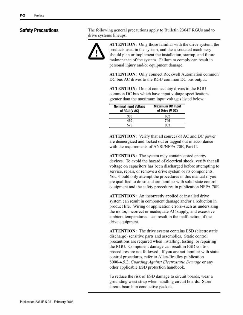
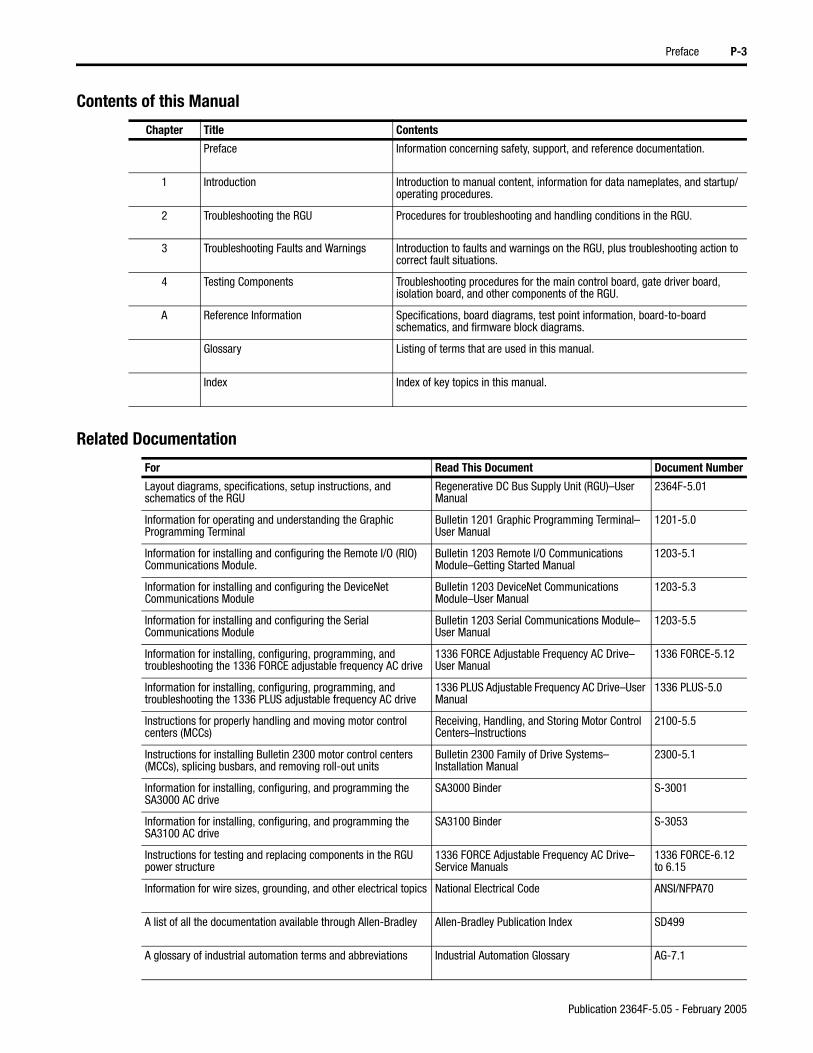
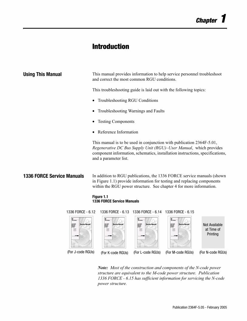
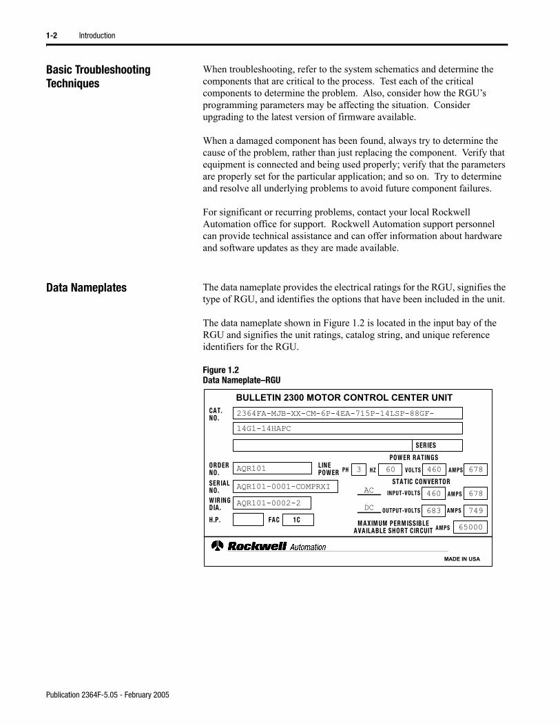
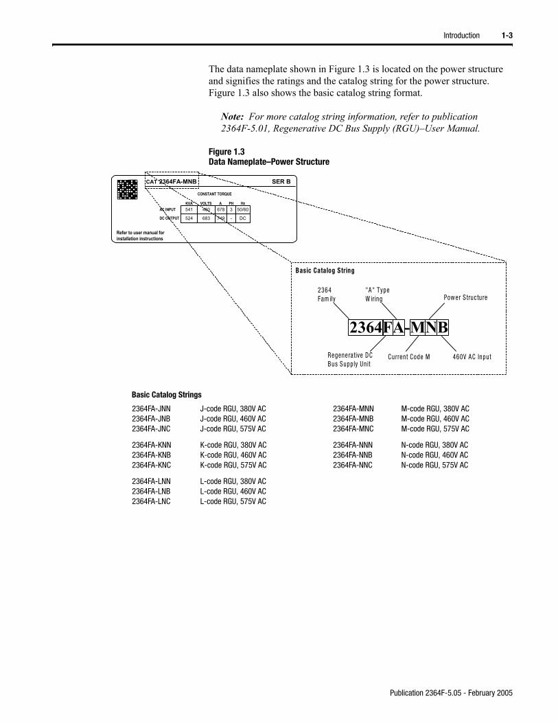
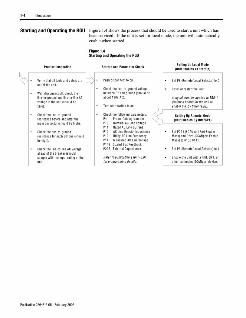
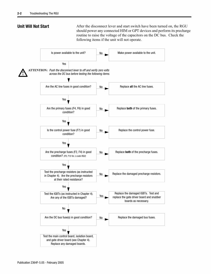
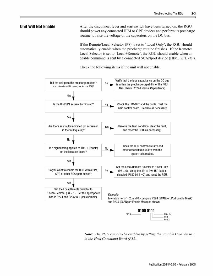
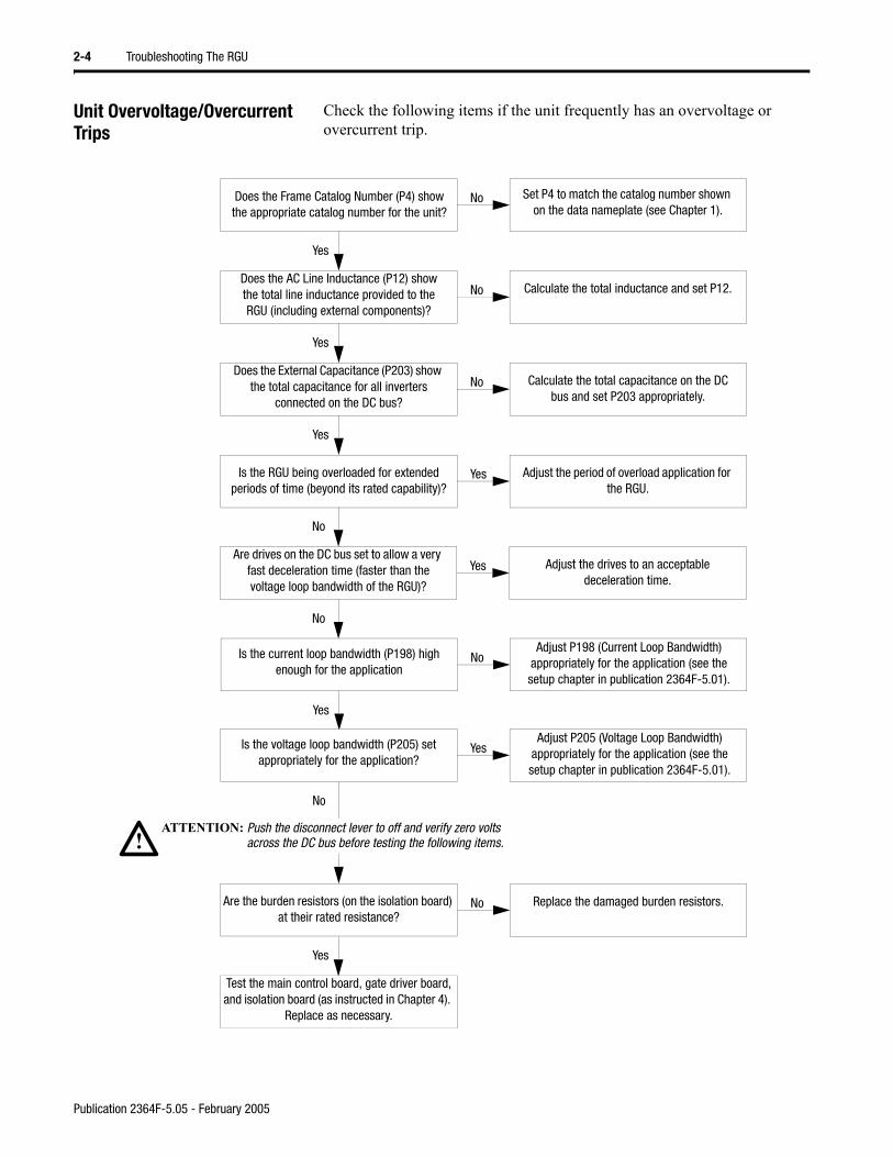
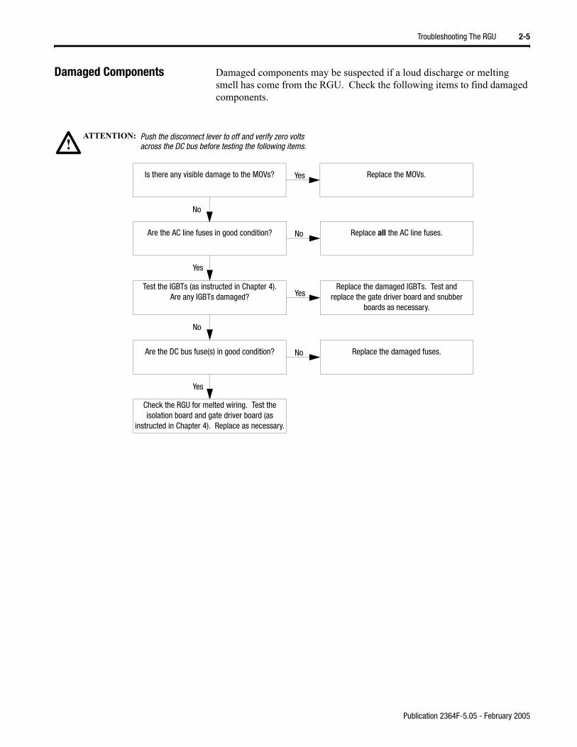
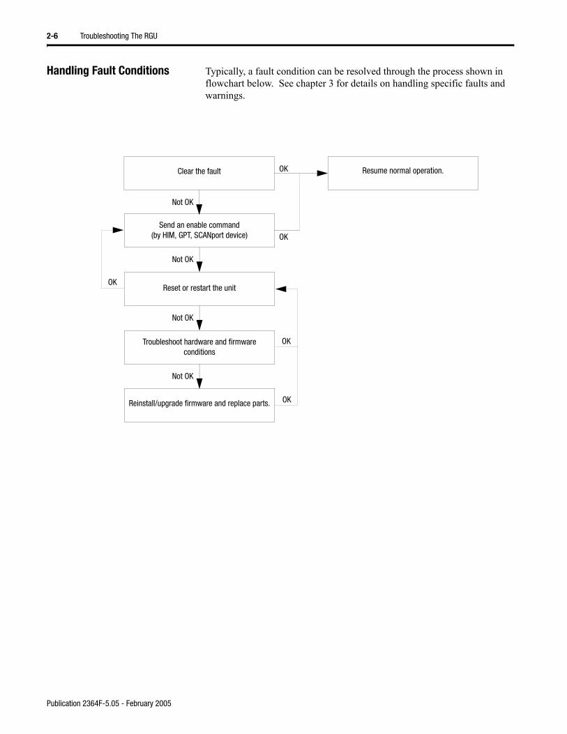
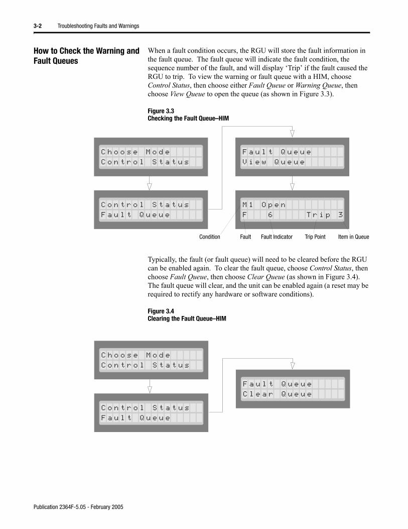
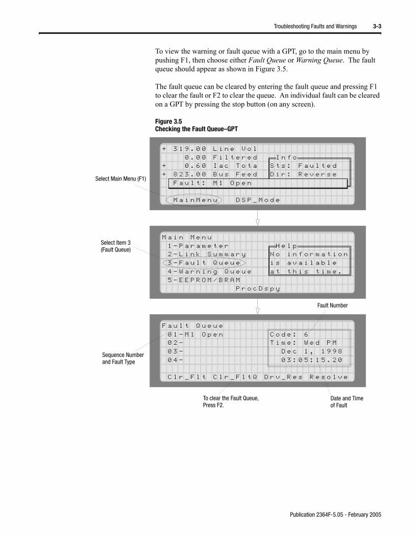
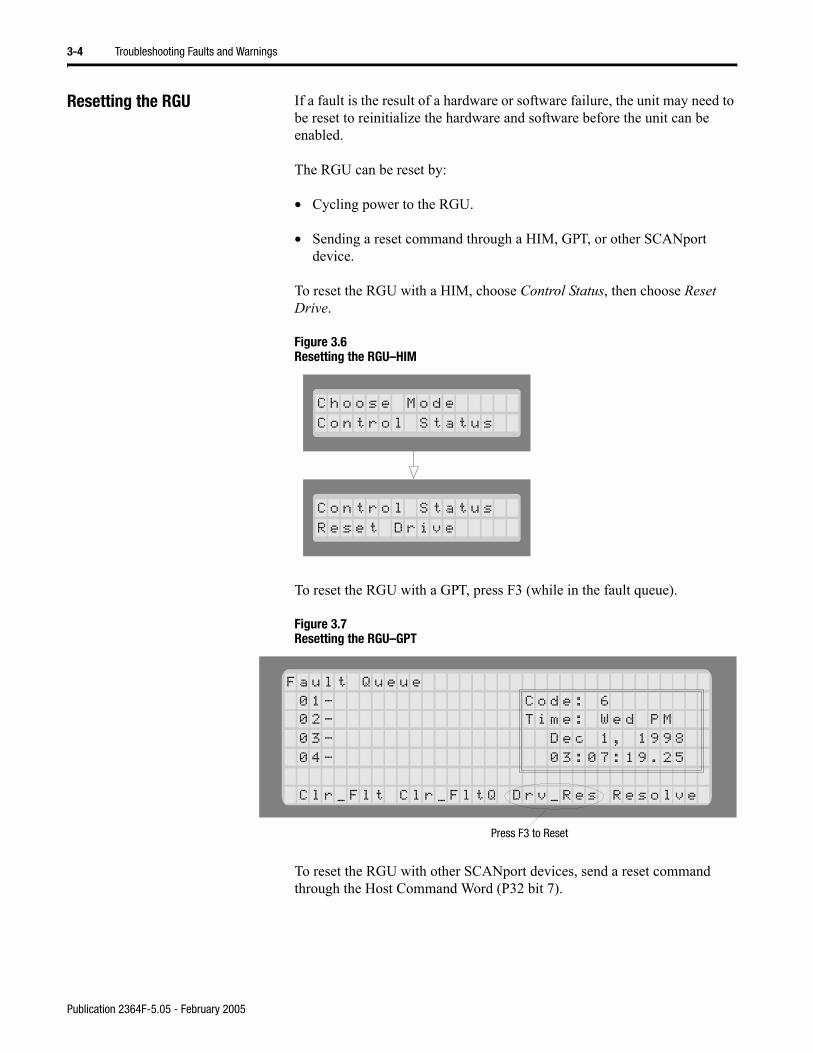
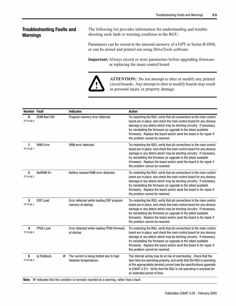
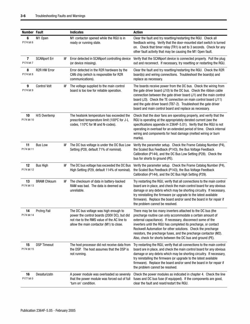
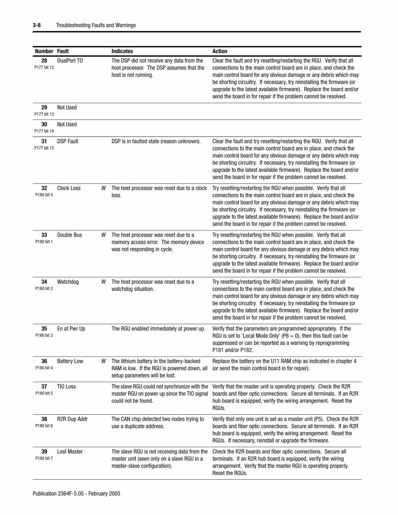
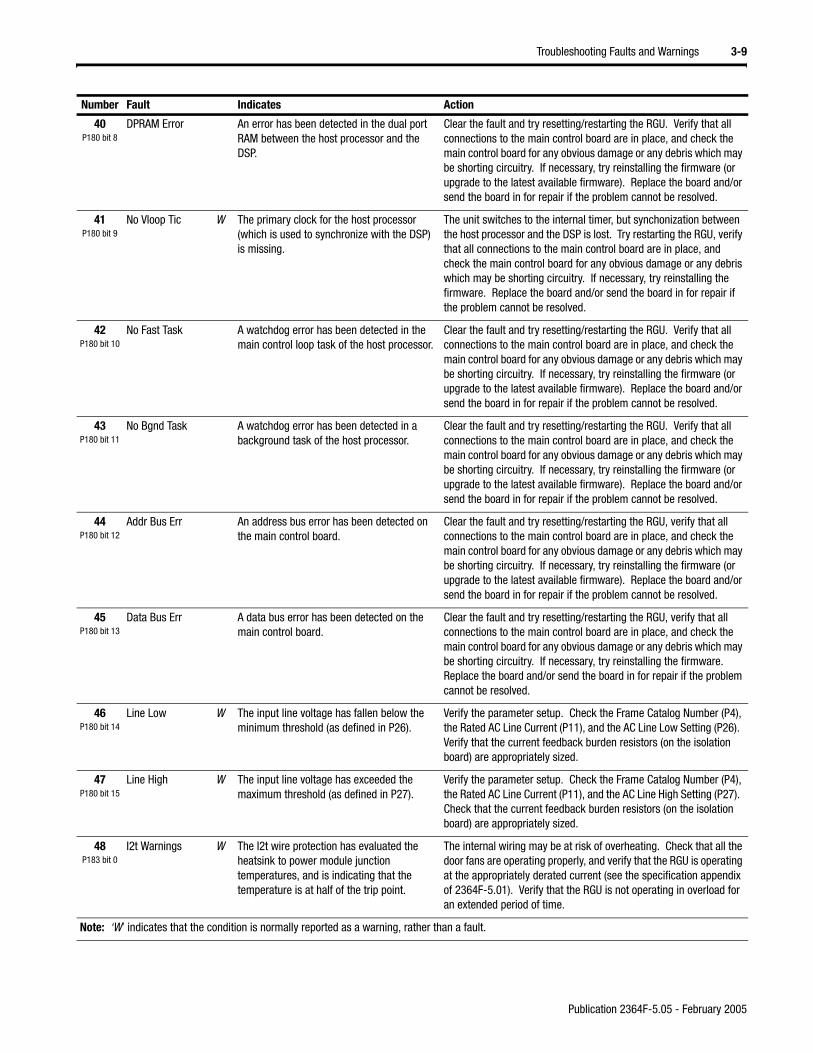
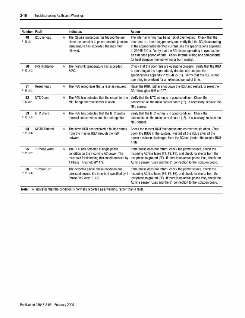
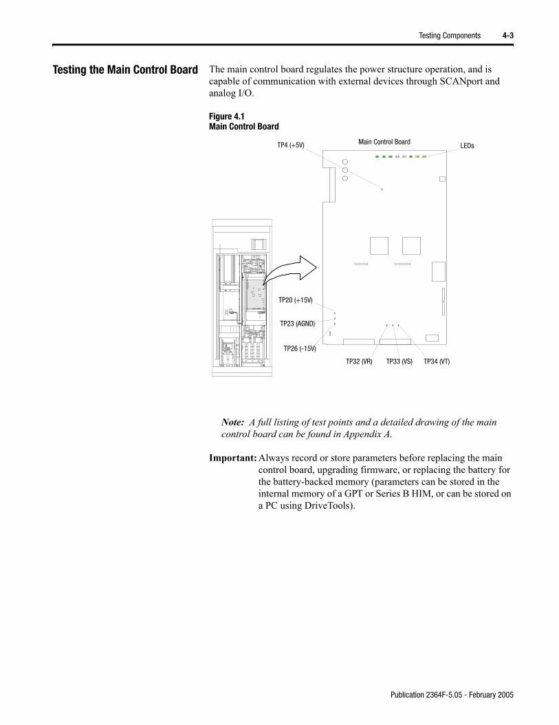
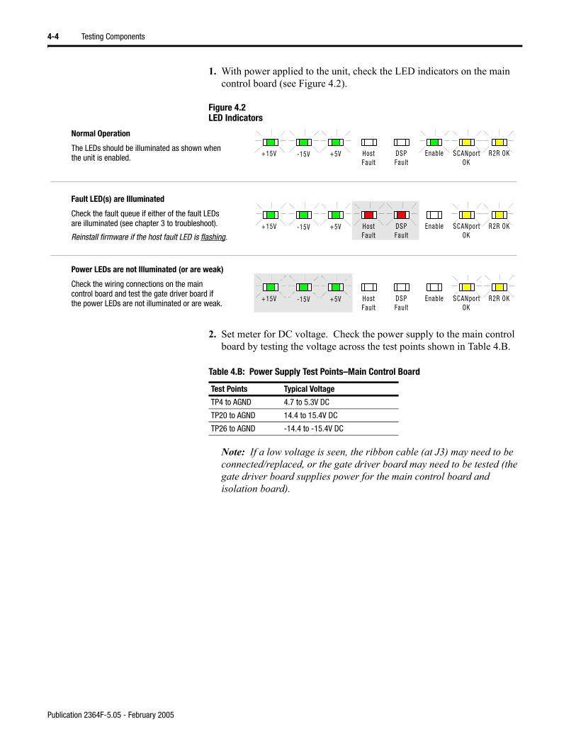
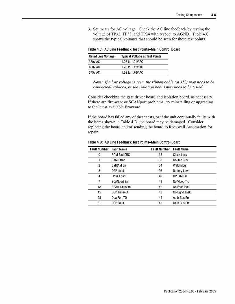
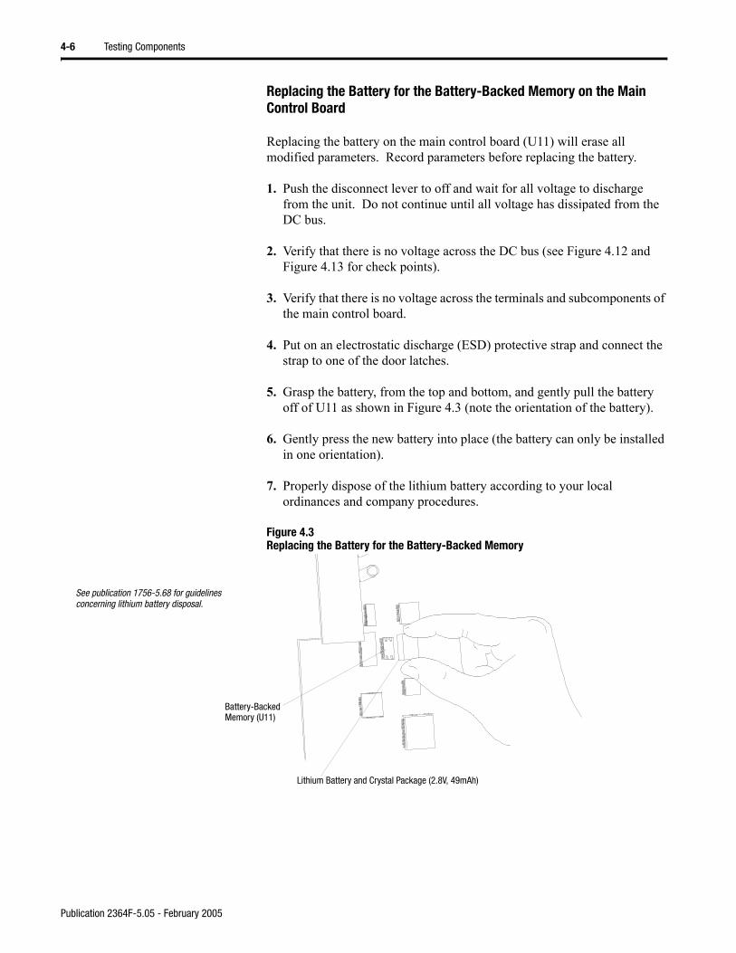
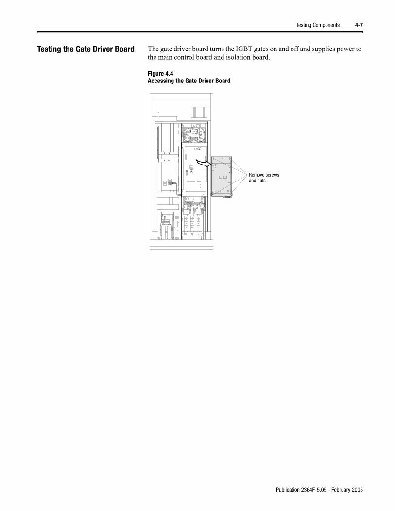
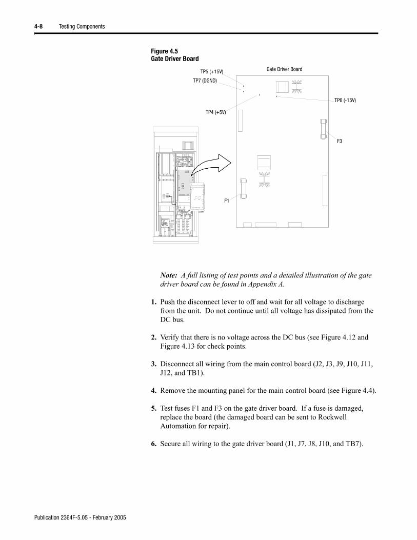
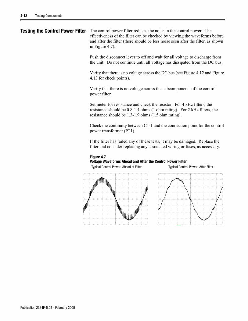
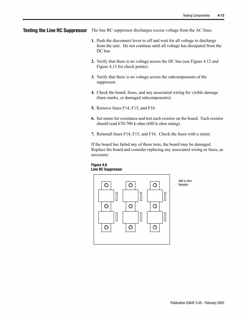
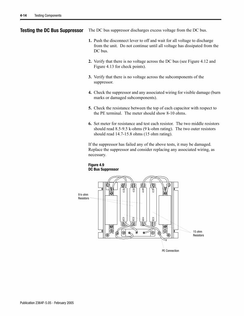
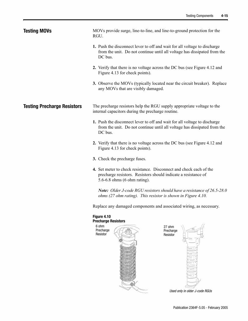
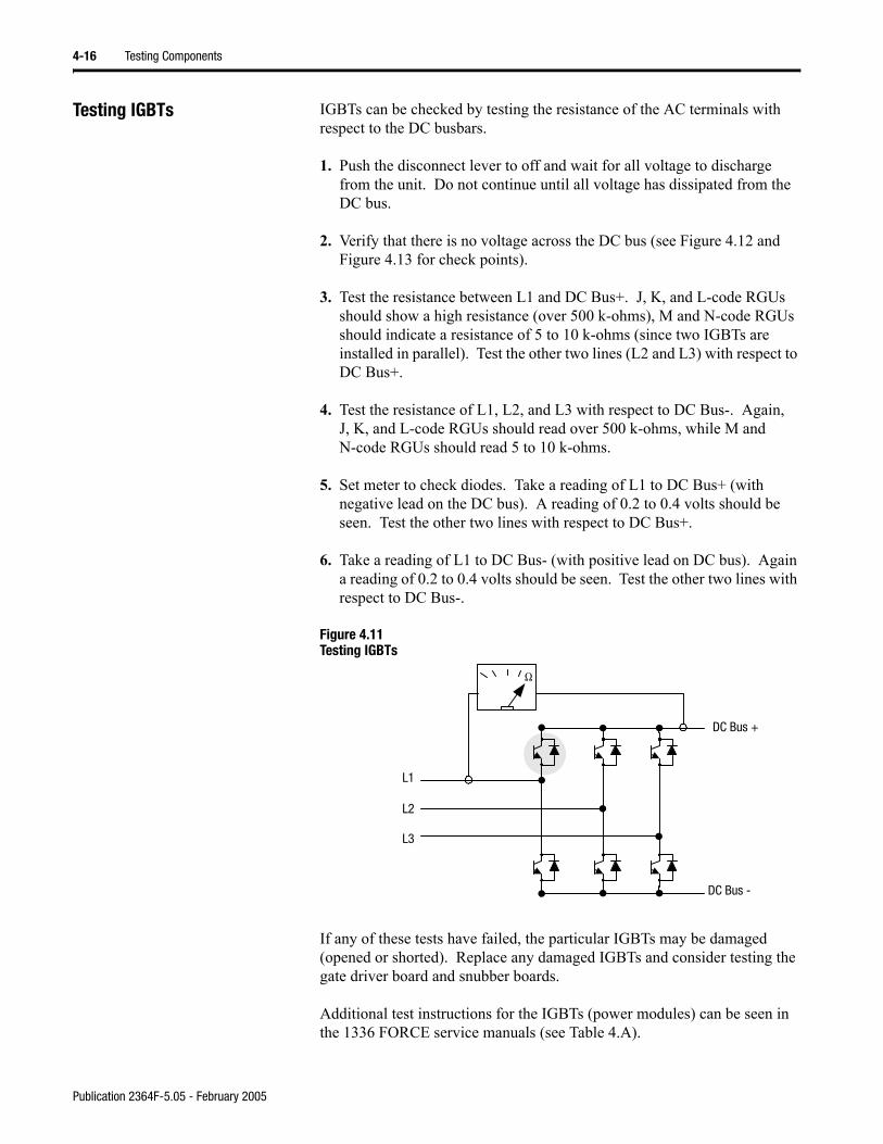
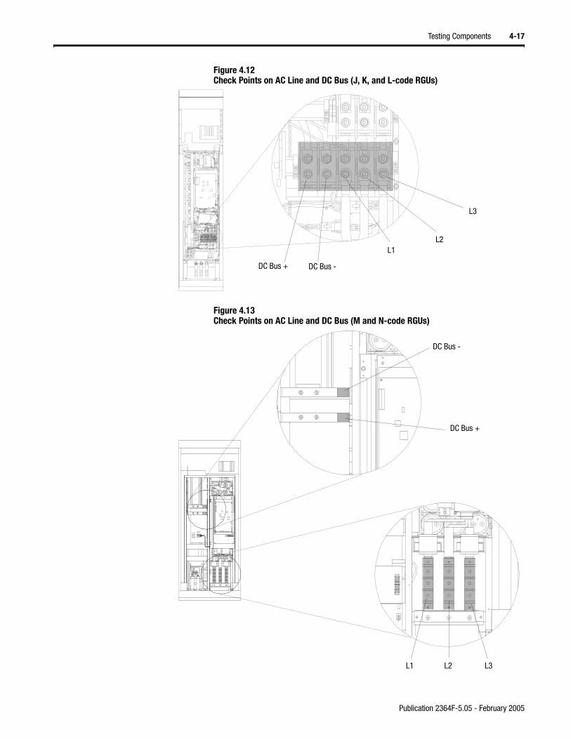
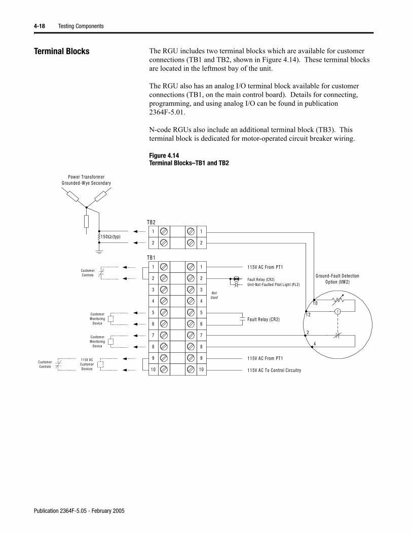
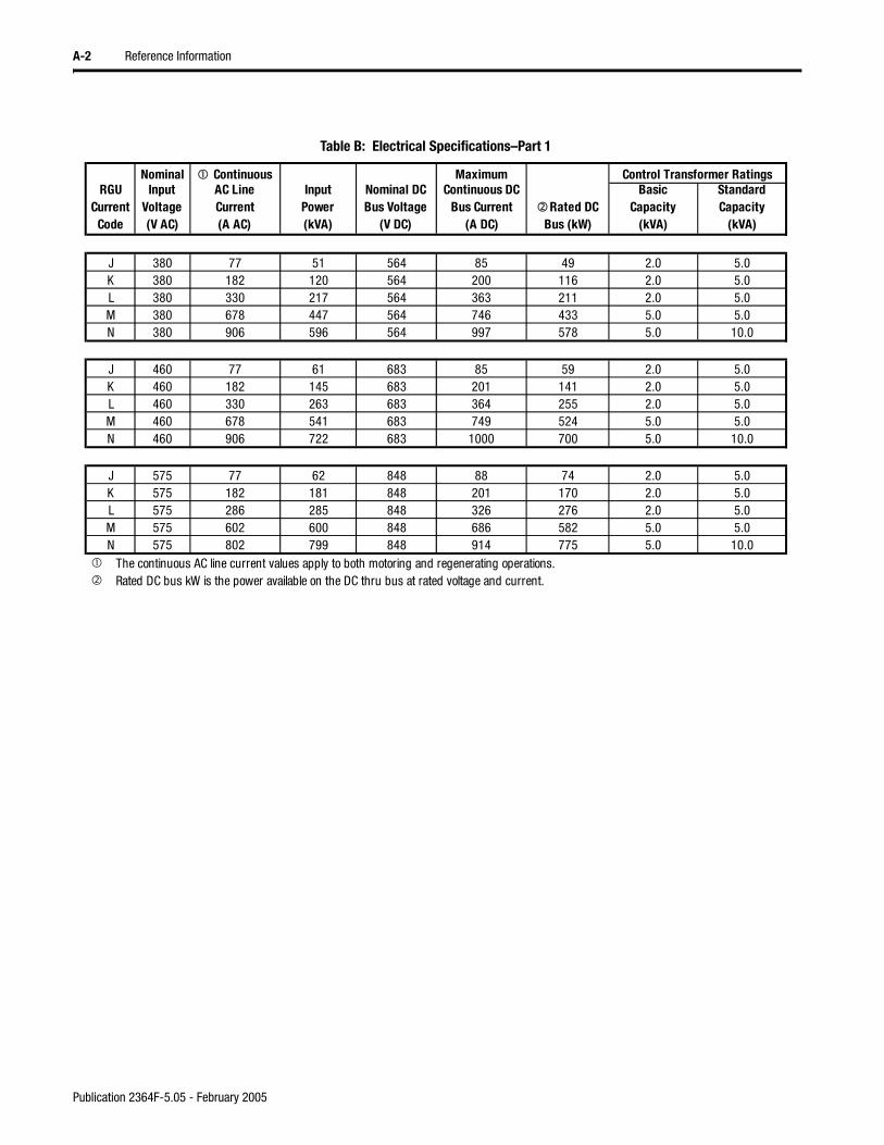
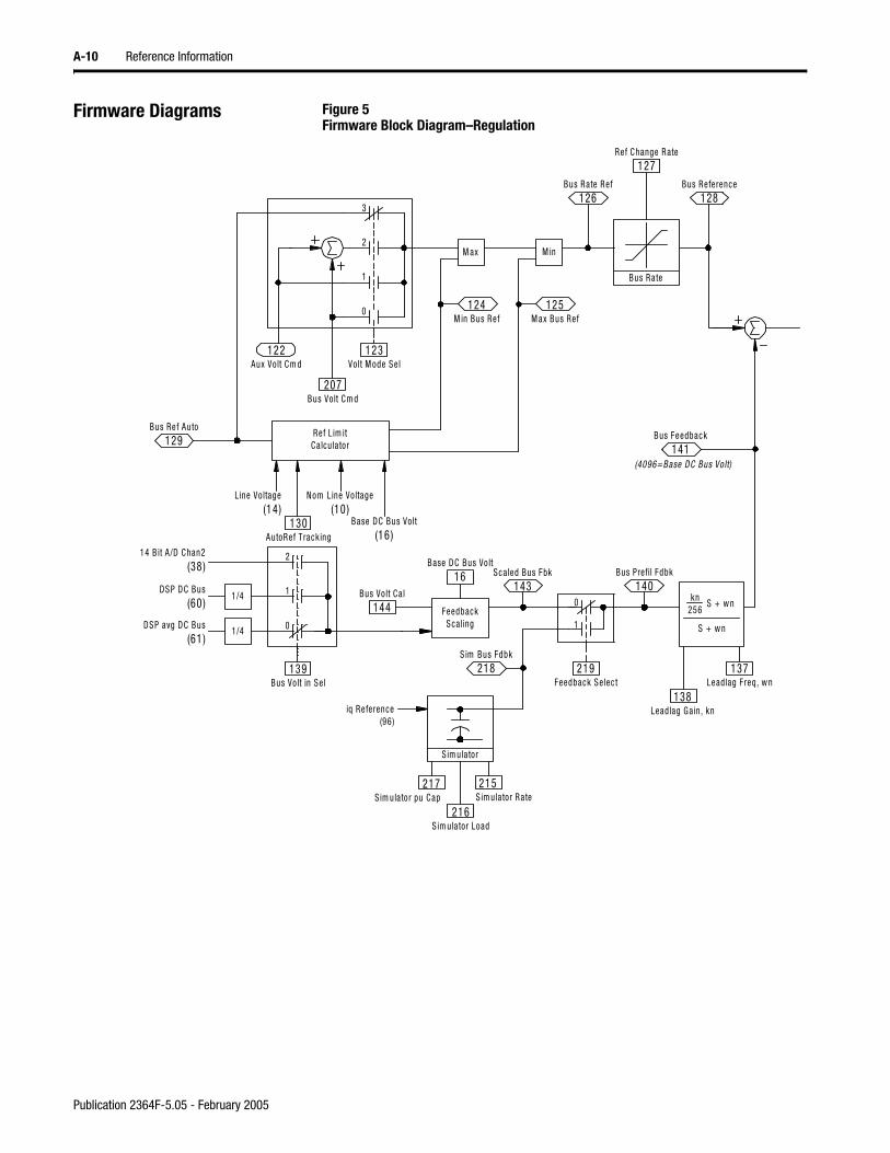
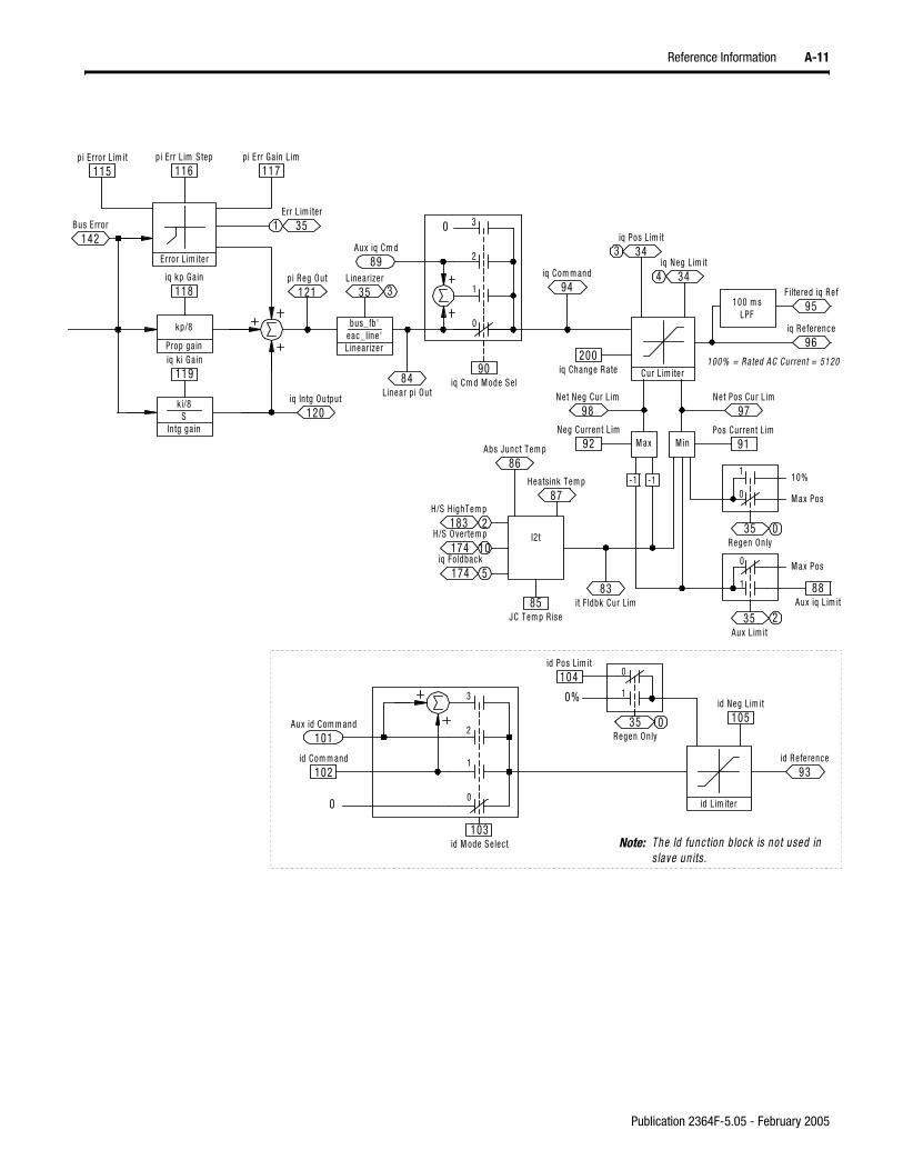
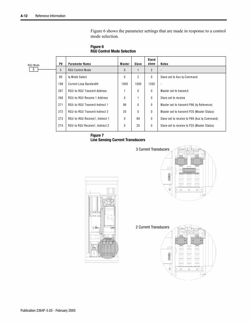

Index I-3
Publication 2364F-505 - February 2005
Publication 2364F-505 - February 2005 PN 366075-P01Supersedes Publication 2364F-505 - March 1999 copy2005 Rockwell International Corporation Printed in the USA
| Print On Demand Specifications | Last Revision 43004 | |||
| Publication | 2364F-TG000B-EN-P (2364F-505 February 2005) | |||
| Quantity | Specified by Buyer | |||
| Sides | Double-sided | |||
| Body Page Count | 60 | |||
| Stock Weight - Body | 20 bond | |||
| Ink - Body | Black | |||
| Cover Count | 4 | |||
| Stock Weight - Cover | 90 Bristol Index | |||
| Ink - Cover | Black (1-1-0-1) | |||
| Binding | Tape bind (52-220 pages26-110 sheets) | |||
| Drilling | Three Hole | |||
| Folding | Based on binding method | |||
| Trim Size | 85 x 11 inches (Nominal) | |||
| File Sent | ||||
| Packaging | Per vendor standard method | |||
| Delivery | Specified by Buyer |
| Offset Print Specifications | Last Revision 43004 | |||
| Publication | 2364F-TG000B-EN-P (2364F-505 February 2005) | |||
| Quantity | Specified by Buyer | |||
| Sides | Double-sided | |||
| Body Page Count | 60 | |||
| Stock Weight - Body | 50 smooth white offset (house stock) | |||
| Ink - Body | Black | |||
| Cover Count | 4 | |||
| Stock Weight - Cover | 8-10 pt coated 1S (house weight amp stock) | |||
| Ink - Cover | Black and PMS 187 red aqueous coated (2-1-0-1) | |||
| Binding | Perfect bind (120 pages minimum) | |||
| Drilling | Three Hole | |||
| Folding | Based on binding method | |||
| Trim Size | 85 x 11 inches (Nominal) | |||
| File Sent | ||||
| Packaging | Specified by Buyer | |||
| Delivery | Specified by Buyer |
| PDF Job Options | Last Revison 93003 | |||||
| Tab | Description | |||||
| General | File Options | |||||
| Compatibility | Acrobat 30 | |||||
| 3 | Optimized PDF | |||||
| Resolution | 1200 dpi | |||||
| Binding | Left | |||||
| Compression | Color Bitmap Images | |||||
| 3 | Bicubic Downsampling at | 150 dpi | ||||
| 3 | Compression | Automatic | ||||
| Quality | Medium | |||||
| Grayscale Bitmap Images | ||||||
| 3 | Bicubic Downsampling at | 150 dpi | ||||
| 3 | Compression | Automatic | ||||
| Quality | Medium | |||||
| Monochrome Bitmap Images | ||||||
| 3 | Bicubic Downsampling at | 300 dpi | ||||
| 3 | Compression | CCITT Group 4 | ||||
| 3 | Compress Text and Line Art | |||||
| Fonts | 3 | Embed All Fonts | ||||
| 3 | Subset All Embedded Fonts Below | 100 | ||||
| When Embedding Fails | Warn and Continue | |||||
| Embedding | Base 14 Fonts | |||||
| Color | Conversion | |||||
| 3 | Leave Color Unchanged | |||||
| Options | ||||||
| 3 | Preserve Overprint Settings | |||||
| 3 | Preserve Under Color Removal amd Black Generation | |||||
| 3 | Preserve Transfer Functions | |||||
| Advanced | Options | |||||
| 3 | Preserve Level 2 copypage Semantics | |||||
| Document Structuring Convensions (DSC) | ||||||
| 3 | Process DSC | |||||
| 3 | Preserve EPS Info from DSC | |||||
| 3 | Preserve OPI Comments | |||||
| 3 | Preserve Document Info from DSC | |||||
| Default Page Size | ||||||
| Width | 612 | |||||
| Heigth | 792 | |||||
| Units | Points |

Index I-3
Publication 2364F-505 - February 2005
Publication 2364F-505 - February 2005 PN 366075-P01Supersedes Publication 2364F-505 - March 1999 copy2005 Rockwell International Corporation Printed in the USA
| Print On Demand Specifications | Last Revision 43004 | |||
| Publication | 2364F-TG000B-EN-P (2364F-505 February 2005) | |||
| Quantity | Specified by Buyer | |||
| Sides | Double-sided | |||
| Body Page Count | 60 | |||
| Stock Weight - Body | 20 bond | |||
| Ink - Body | Black | |||
| Cover Count | 4 | |||
| Stock Weight - Cover | 90 Bristol Index | |||
| Ink - Cover | Black (1-1-0-1) | |||
| Binding | Tape bind (52-220 pages26-110 sheets) | |||
| Drilling | Three Hole | |||
| Folding | Based on binding method | |||
| Trim Size | 85 x 11 inches (Nominal) | |||
| File Sent | ||||
| Packaging | Per vendor standard method | |||
| Delivery | Specified by Buyer |
| Offset Print Specifications | Last Revision 43004 | |||
| Publication | 2364F-TG000B-EN-P (2364F-505 February 2005) | |||
| Quantity | Specified by Buyer | |||
| Sides | Double-sided | |||
| Body Page Count | 60 | |||
| Stock Weight - Body | 50 smooth white offset (house stock) | |||
| Ink - Body | Black | |||
| Cover Count | 4 | |||
| Stock Weight - Cover | 8-10 pt coated 1S (house weight amp stock) | |||
| Ink - Cover | Black and PMS 187 red aqueous coated (2-1-0-1) | |||
| Binding | Perfect bind (120 pages minimum) | |||
| Drilling | Three Hole | |||
| Folding | Based on binding method | |||
| Trim Size | 85 x 11 inches (Nominal) | |||
| File Sent | ||||
| Packaging | Specified by Buyer | |||
| Delivery | Specified by Buyer |

Index I-3
Publication 2364F-505 - February 2005
Publication 2364F-505 - February 2005 PN 366075-P01Supersedes Publication 2364F-505 - March 1999 copy2005 Rockwell International Corporation Printed in the USA
| Print On Demand Specifications | Last Revision 43004 | |||
| Publication | 2364F-TG000B-EN-P (2364F-505 February 2005) | |||
| Quantity | Specified by Buyer | |||
| Sides | Double-sided | |||
| Body Page Count | 60 | |||
| Stock Weight - Body | 20 bond | |||
| Ink - Body | Black | |||
| Cover Count | 4 | |||
| Stock Weight - Cover | 90 Bristol Index | |||
| Ink - Cover | Black (1-1-0-1) | |||
| Binding | Tape bind (52-220 pages26-110 sheets) | |||
| Drilling | Three Hole | |||
| Folding | Based on binding method | |||
| Trim Size | 85 x 11 inches (Nominal) | |||
| File Sent | ||||
| Packaging | Per vendor standard method | |||
| Delivery | Specified by Buyer |

Index I-3
Publication 2364F-505 - February 2005
Publication 2364F-505 - February 2005 PN 366075-P01Supersedes Publication 2364F-505 - March 1999 copy2005 Rockwell International Corporation Printed in the USA

Publication 2364F-505 - February 2005 PN 366075-P01Supersedes Publication 2364F-505 - March 1999 copy2005 Rockwell International Corporation Printed in the USA


![REGENERATIVE BRAKING SYSTEM IN ELECTRIC VEHICLES · REGENERATIVE BRAKING SYSTEM IN ELECTRIC VEHICLES ... REGENERATIVE BRAKING SYSTEM ... Regenerative action during braking[9]](https://img.pdfslide.us/doc/110x75/5adccef67f8b9a1a088c7cf0/regenerative-braking-system-in-electric-vehicles-braking-system-in-electric-vehicles.jpg)