Embed Size (px)
Citation preview

TRAVELING WAVE TUBE OUTPUT WINDOW MODEL
(IMPEDANCE MATCHING PROBLEM)
Team MembersAnkush Mohan
Gurvinder Dilawari

Project Overview
• Background of HFSS & TWT• Modeling Process• Discoveries / Results• Conclusion

GoalFigure out how to model an output circuit in HFSS and set a Standard Procedure for futuresimulation process.

HFSS Background
• 3D EM Simulation Software Tool for RF, Wireless, Packaging and Optoelectronic Design
• Used for modeling High speed PCB, Package, IC, Antenna, Array Design along with RF and Microwave component design.
HFSS Interface

Traveling Wave Tube (TWT)Overview
• High Frequency Wideband Amplifier • Output Power Ranges from Watt-Mega Watts• Used as final amplifiers In nearly all warfare and satellite communication systems.

The Output Window
• It is a transmission line that matches the impedance from the vacuum to a coax.
• A bad match can cause reflections going back into the tube which can damage the tube itself.

Project Iterations and Learning Aspects
• Capabilities of HFSS were unknown in the beginning.
• Memory Issues.• No one had attempted to model the whole
output circuit before

Pieces Of Our Model
Helix circuit only Dome Window
Matching Fingers Coaxial Connector

Modeling Process
9 Turns-Loss away from Helix 19 Turns-Loss close to Helix
19 Turns & Window 19 Turns, Window & Coax

Initial Plan
S Parameters
• Solve all the pieces separately for their VSWR.
• Combine solutions to solve the whole problem.
• Realized that waveports could not be assigned with S parameter values.
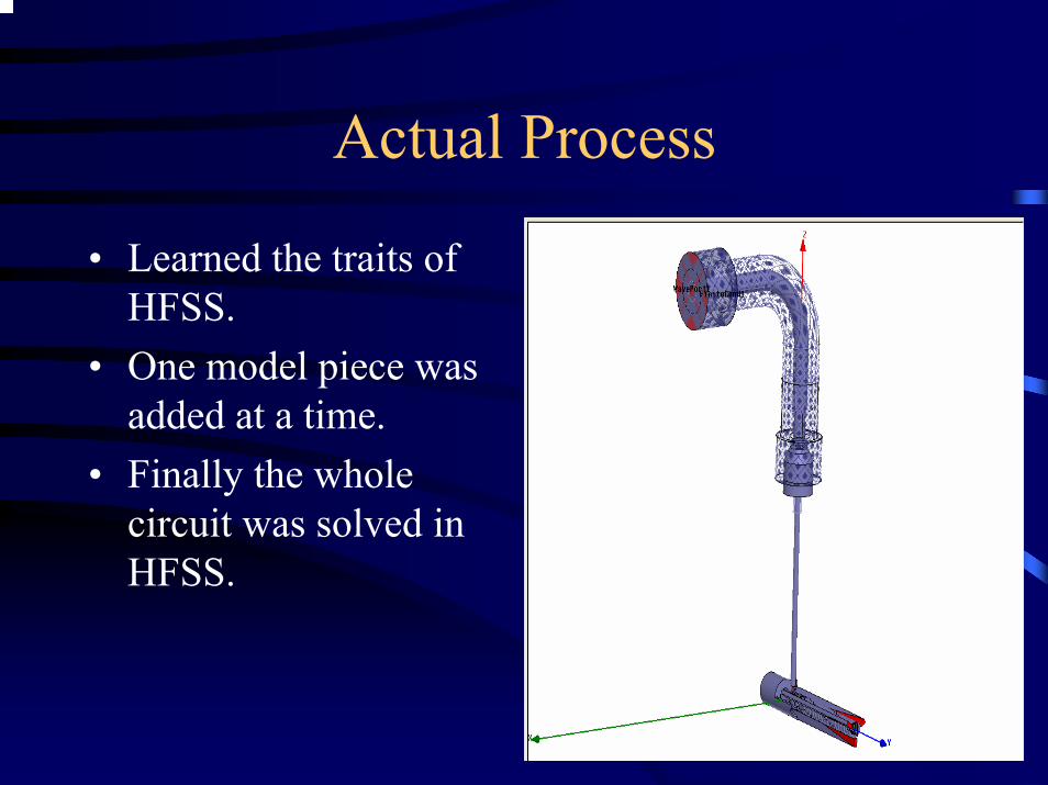
Actual Process
• Learned the traits of HFSS.
• One model piece was added at a time.
• Finally the whole circuit was solved in HFSS.

Critical Modeling Decisions
• How to introduce attenuation in the circuit to make it into a one port device.
• Tape geometry.• Inclusion of Matching Fingers.• Waveguide or Coaxial connector.

Introducing the Attenuation
9 Turns-Loss away from Helix 19 Turns-Loss close to HelixAttenuation Region

Tape Geometry
Circular Tape matched with a real life circuitStraight
Tape

Matching Fingers
Used In Real Circuits To Tune The Impedance Match

Waveguide or Coaxial Connector
Waveguide Coaxial Connector

Discoveries• Small sharp edges
were disliked by HFSS and cause the program to run out of memory.
• Time Domain Reflectometry (TDR).
Sharp Edge
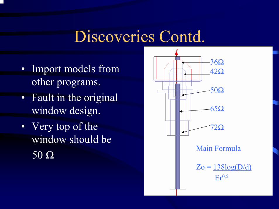
Discoveries Contd.
• Import models from other programs.
• Fault in the original window design.
• Very top of the window should be 50 Ω
36Ω42Ω
50Ω
65Ω
72Ω
Main Formula
Zo = 138log(D/d)Er0.5

Confirmed Original Fault By TDR
• TDR gives us a plot of Impedance of the circuit versus time.
• Calculations were confirmed by the TDR plot of the circuit.
Window Region
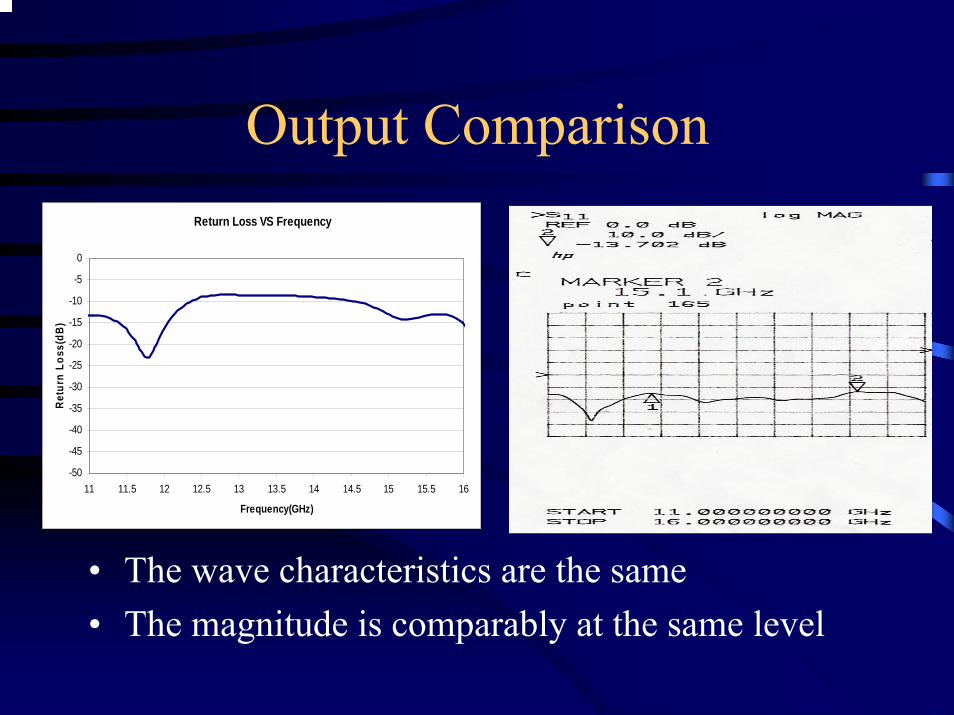
Output ComparisonReturn Loss VS Frequency
-50
-45
-40
-35
-30
-25
-20
-15
-10
-5
0
11 11.5 12 12.5 13 13.5 14 14.5 15 15.5 16
Frequency(GHz)
Retu
rn L
oss(
dB)
• The wave characteristics are the same• The magnitude is comparably at the same level

Conclusion
• Figured out how to model the Output Circuit successfully.
• Findings will be used as future reference for modeling output circuits.
• Increase efficiency of new designs

Questions?


![[SJSU] Social Media Strategy](https://img.pdfslide.us/doc/110x75/559793dc1a28abdd108b467c/sjsu-social-media-strategy.jpg)