Embed Size (px)
Citation preview

Transition-Edge Sensors for BES needs
Joel Ullom
Project Leader, Quantum Calorimeters
NIST
Boulder, Colorado

Members of NIST Quantum Sensors Program
James Beall Dan Becker Doug Bennett Hsiao-Mei (Sherry) Cho Ed Denison Randy Doriese Lisa Ferreira Colin Fitzgerald Anna Fox Jiansong Gao Gene Hilton Rob Horansky Kent Irwin Zhao Kang Vince Kotsubo
Dale Li Peter Lowell Ben Mates Galen O’Neil Mike Niemack Omid Noroozian Carl Reintsema Frank Schima Dan Schmidt Dan Swetz Jens Uhlig Leila Vale Jeff Van Lanen Yizi Xu
NIST - Boulder NIST – Gaithersburg/BNL
Dan Fischer Cherno Jaye

Core technology: Transition-Edge Sensor (TES) calorimeter
0.06
96 96.2
temperature (mK)
resi
stan
ce (Ω
)
0.00 95.8
thin-film thermometer TES micrograph
SiN
current
Mo/Cu bilayer TES with additional normal features
0.5 mm
DE =x kbT2C

Core technology: SQUID readout SQUIDS = versatile, low noise current amplifiers that provide useful signal gain between superconducting sensors and conventional electronics
0.2 mm
SQUID current amplifier
V
I
T, R, and I
change
TES bias circuit
NIST SQUIDS fabricated into superconducting integrated circuits for readout of sensor arrays
32:1 and 1,312:32 multiplexer circuits for TDM or Φ-CDM
TES 1
TES 2
TES 4
TES 3
new I-CDM circuit for ~ 106 pix arrays μwave SQUID readout for ~ 105 pix arrays
75 mm
20 mm
(Stiehl, APL 2012) (Mates, APL 2008)
(Irwin, JLTP 2012)

Why care?
TES calorimeters can provide a unique combination of spectral resolution and efficiency
240Pu 239Pu
energy-dispersive gamma-ray detectors
TES

NIST TES array
• 256 pixel TES gamma-ray spectrometer. Active area = 5.76 cm2, similar to planar germanium sensor. World’s largest calorimeter array.
• To absorb gamma-rays, bulk Sn absorbers are hybridized to thin-film TES circuitry.
• -pair breaking changes surface impedance of superconductor
• -film embedded in μwave resonator
0.06
96 96.2
temperature (mK)
resi
stan
ce (Ω
)
0.00 95.8
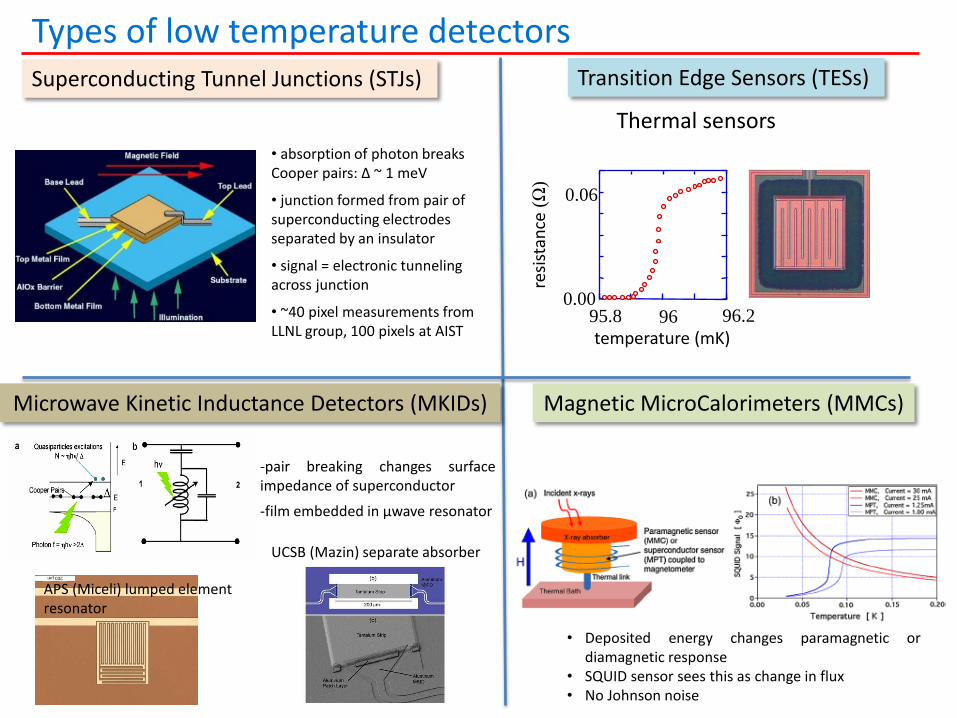
Types of low temperature detectors Superconducting Tunnel Junctions (STJs) Transition Edge Sensors (TESs)
Microwave Kinetic Inductance Detectors (MKIDs) Magnetic MicroCalorimeters (MMCs)
Thermal sensors
• absorption of photon breaks Cooper pairs: Δ ~ 1 meV
• junction formed from pair of superconducting electrodes separated by an insulator
• signal = electronic tunneling across junction
• ~40 pixel measurements from LLNL group, 100 pixels at AIST
APS (Miceli) lumped element resonator
UCSB (Mazin) separate absorber
• Deposited energy changes paramagnetic or diamagnetic response
• SQUID sensor sees this as change in flux • No Johnson noise

Superconducting Tunnel Junctions (STJs) Transition Edge Sensors (TESs)
Microwave Kinetic Inductance Detectors (MKIDs)
Magnetic MicroCalorimeters (MMCs)
• ΔE ~ 5 eV @ 1 keV, > 10 eV above 1 keV
• High per pixel count rates: ~ 10 kHz
• No multiplexing technology:
arrays limited to ~102 pixels
• No leverage from other applications
Types of low temperature detectors

• Best achieved resolutions:
ΔE =1.6 eV @ 6 keV, 22 eV @ 97 keV
• Per pixel count rates: ≤ 300 Hz
• Largest achieved arrays: 256 (X) 104 pixels (Far IR)
• Compatible w/ μwave readout: path to 106 pix arrays
• Most efficient use of readout bandwidth:
hybrid multiplexer architecture
• More complicated fabrication
• Extensive leverage from other applications
Superconducting Tunnel Junctions (STJs) Transition Edge Sensors (TESs)
Microwave Kinetic Inductance Detectors (MKIDs)
Magnetic MicroCalorimeters (MMCs)
• ΔE ~ 5 eV @ 1 keV, > 10 eV above 1 keV
• High per pixel count rates: ~ 10 kHz
• No multiplexing technology:
arrays limited to ~102 pixels
• No leverage from other applications
• Successful in Far IR and visible
• Achieved X-ray resolution: 62 eV @ 6 keV
obstacles to very good ΔE, solvable?
• Per pixel count rates: 500-1000 Hz
• Achieved arrays: few (X), 103 (visible, Far IR)
• Compatible w/ μwave readout:
path to 106 pix arrays
• Simpler fabrication
• Achieved resolutions similar to TES
• Resolution limits ~ 2x better than TES
• Count rates similar to TES
• Very early multipixel demonstrations
• Multiplexing possible, harder than TESs
• Readout easily degrades resolution
• Compatible w/ μwave readout: path to 106 pix arrays
• Fabrication similar to TES
Types of low temperature detectors
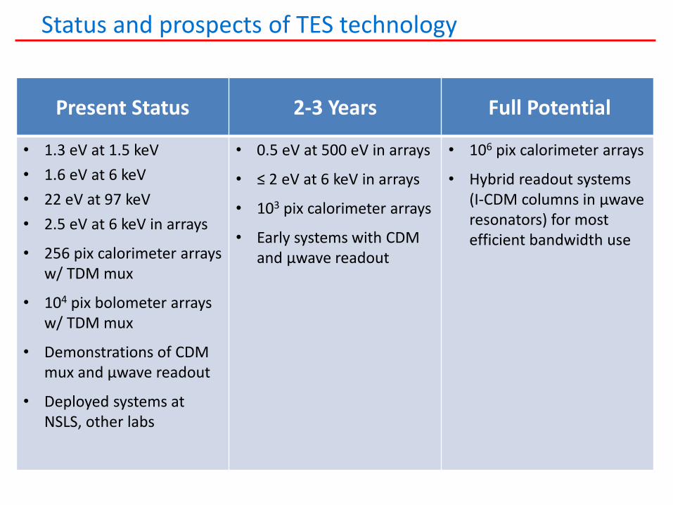
Status and prospects of TES technology
W Si
Present Status 2-3 Years Full Potential
• 1.3 eV at 1.5 keV
• 1.6 eV at 6 keV
• 22 eV at 97 keV
• 2.5 eV at 6 keV in arrays
• 256 pix calorimeter arrays w/ TDM mux
• 104 pix bolometer arrays w/ TDM mux
• Demonstrations of CDM mux and μwave readout
• Deployed systems at NSLS, other labs
• 0.5 eV at 500 eV in arrays
• ≤ 2 eV at 6 keV in arrays
• 103 pix calorimeter arrays
• Early systems with CDM and μwave readout
• 106 pix calorimeter arrays
• Hybrid readout systems (I-CDM columns in μwave resonators) for most efficient bandwidth use
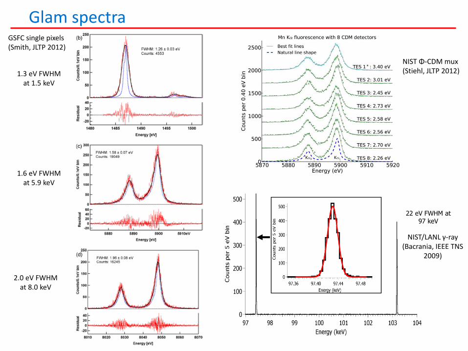
Glam spectra
W Si
GSFC single pixels (Smith, JLTP 2012)
1.3 eV FWHM at 1.5 keV
1.6 eV FWHM at 5.9 keV
2.0 eV FWHM at 8.0 keV
NIST Φ-CDM mux (Stiehl, JLTP 2012)
22 eV FWHM at 97 keV
NIST/LANL γ-ray (Bacrania, IEEE TNS
2009)

Areas of scientific opportunity
1. X-ray science below 10 keV
2. Compton scattering near 100 keV 1. Time-resolved X-ray measurements at beamlines, and in the laboratory
W Si

X-ray science below 10 keV • TES X-ray spectrometer that can accommodate 256 pixels deployed to National Synchrotron Light
Source (spectrometer paid for by NIST)
• 40 pixels now, 160 in FY13

Immediate applications of prototype NSLS spectrometer:
• partial-fluorescence-yield absorption spectroscopy
• XES of eV-scale chemical shifts
Let’s see an example of each! 50 mK stage and 3 concentric radiation shields that go through 6” ConFlat flange
TES microcalorimeter spectrometer

PFY-NEXAFS
first example application:
partial-fluorescence-yield near-edge X-ray absorption fine structure
(PFY-NEXAFS)
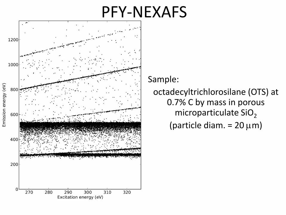
PFY-NEXAFS A difficult sample for U7A:
NIST standard reference material (SRM) 1216-I
Sample:
octadecyltrichlorosilane (OTS) at 0.7% C by mass in porous
microparticulate SiO2
(particle diam. = 20 mm)

monochromator is scanned from 265 to 327 eV
PFY-NEXAFS
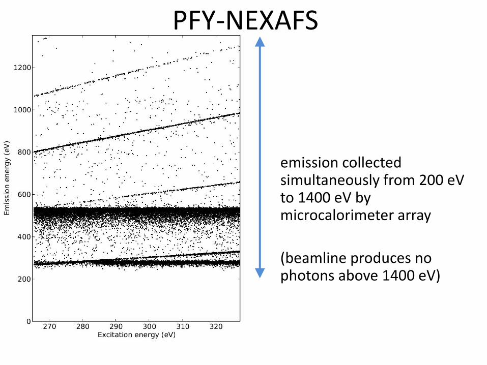
emission collected simultaneously from 200 eV to 1400 eV by microcalorimeter array
(beamline produces no photons above 1400 eV)
PFY-NEXAFS
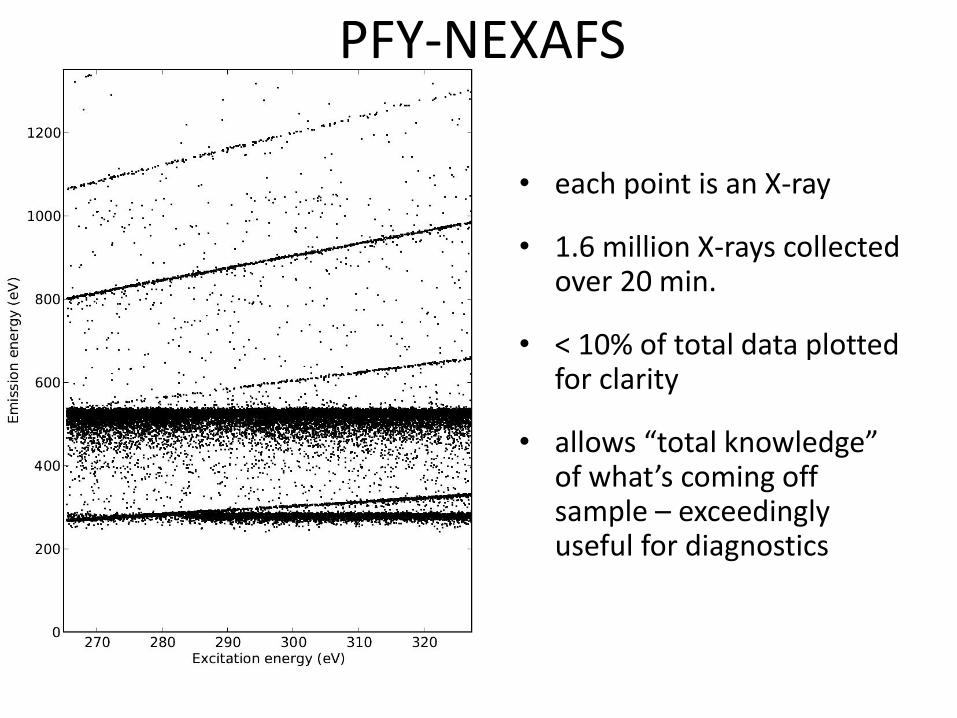
• each point is an X-ray
• 1.6 million X-rays collected over 20 min.
• < 10% of total data plotted for clarity
• allows “total knowledge” of what’s coming off sample – exceedingly useful for diagnostics
PFY-NEXAFS

harmonics 1 – 5 of scattered beam
PFY-NEXAFS
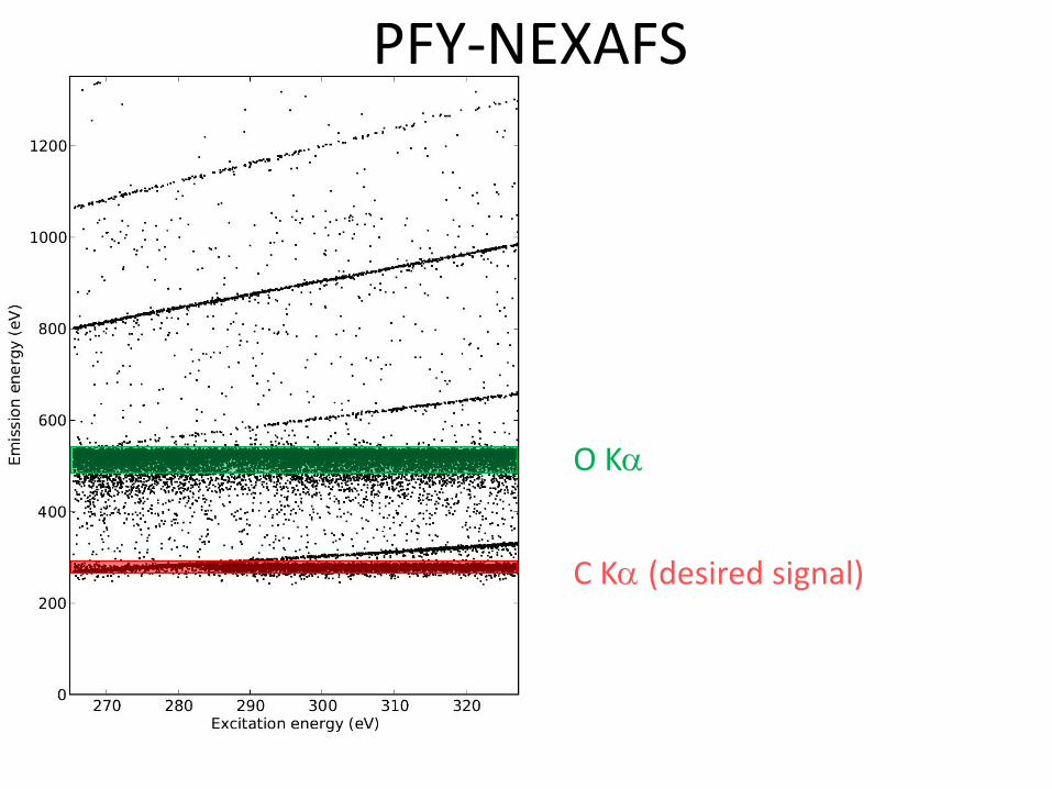
O Ka
C Ka (desired signal)
PFY-NEXAFS

zoom on region typically covered by RIXS map
PFY-NEXAFS

PFY-NEXAFS
zoom on region typically covered by RIXS map
PFY-NEXAFS

PFY-NEXAFS
window on C Ka
(can adjust window after acquisition)
PFY-NEXAFS

octadecyltrichlorosilane (OTS) C18H37Cl3Si 0.7% C (by mass) in SiO2
scattered beam
resulting NEXAFS spectrum
PFY-NEXAFS Spectrum
• better than MultiLayer Mirror (MLM) spectrum of same sample
• Unlike MLM, also works at N, O, … all other edges
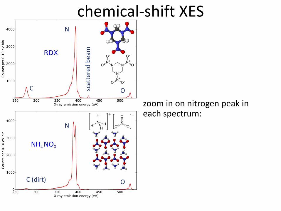
chemical-shift XES
second example application:
X-ray emission spectroscopy (XES) for chemical analysis
chemical-shift XES
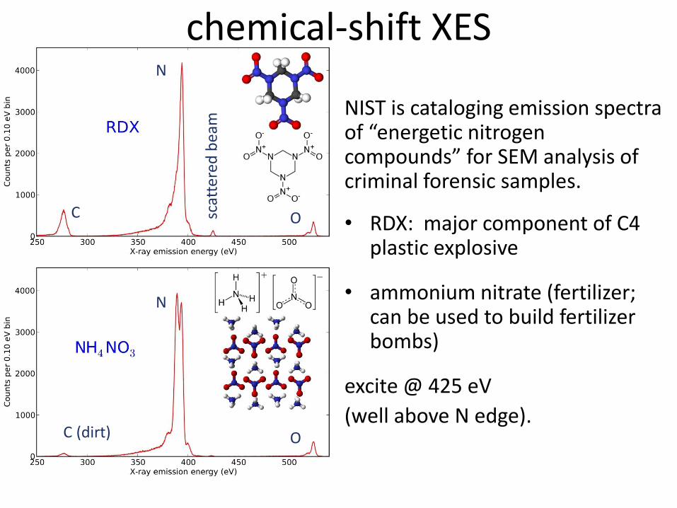
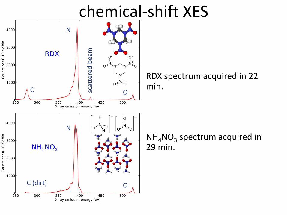
C (dirt) O
N
C
N
O scat
tere
d b
eam
NIST is cataloging emission spectra of “energetic nitrogen compounds” for SEM analysis of criminal forensic samples.
• RDX: major component of C4 plastic explosive
• ammonium nitrate (fertilizer; can be used to build fertilizer bombs)
excite @ 425 eV
(well above N edge).
C (dirt) O
N
C
N
O scat
tere
d b
eam
RDX spectrum acquired in 22 min.
NH4NO3 spectrum acquired in 29 min.
chemical-shift XES
C (dirt) O
N
C
N
O scat
tere
d b
eam
zoom in on nitrogen peak in each spectrum:
chemical-shift XES
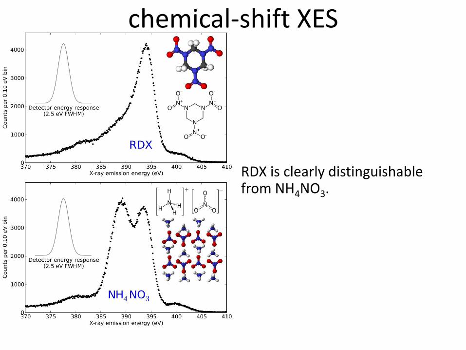
RDX is clearly distinguishable from NH4NO3.
chemical-shift XES

further, NH4NO3 has four resolvable features that are associated with:
• NH4+ (highly reduced)
(2, 3)
• NO3– (highly oxidized)
(1, 3, 4)
(feature ID’s from F.D. Vila, et al., J Phys. Chem. A, 115, 3243-3250 [2011]) 1
2 3
4
chemical-shift XES
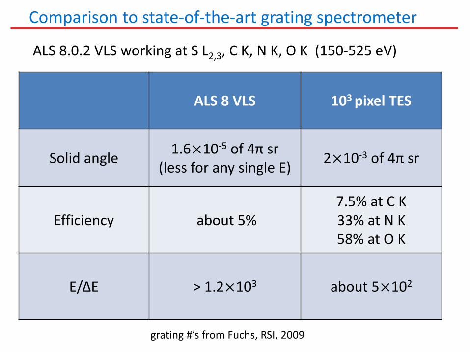
Comparison to state-of-the-art grating spectrometer
ALS 8.0.2 VLS working at S L2,3, C K, N K, O K (150-525 eV)
Si
ALS 8 VLS 103 pixel TES
Solid angle 1.6✕10-5 of 4π sr
(less for any single E) 2✕10-3 of 4π sr
Efficiency about 5% 7.5% at C K 33% at N K 58% at O K
E/ΔE > 1.2✕103 about 5✕102
grating #’s from Fuchs, RSI, 2009
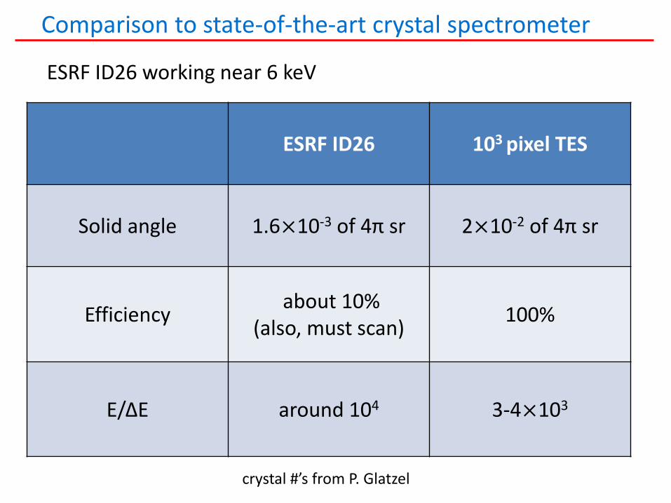
Comparison to state-of-the-art crystal spectrometer
ESRF ID26 working near 6 keV
Si
ESRF ID26 103 pixel TES
Solid angle 1.6✕10-3 of 4π sr 2✕10-2 of 4π sr
Efficiency about 10%
(also, must scan) 100%
E/ΔE around 104 3-4✕103
crystal #’s from P. Glatzel
Strengths of X-ray TESs for beamline science
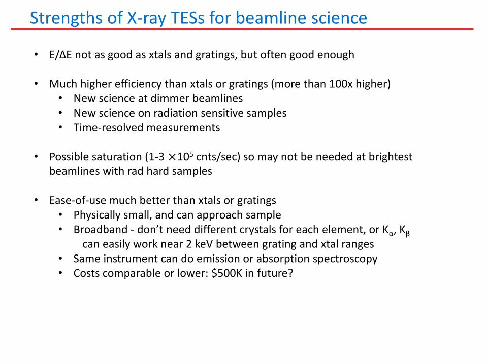
• E/ΔE not as good as xtals and gratings, but often good enough
• Much higher efficiency than xtals or gratings (more than 100x higher) • New science at dimmer beamlines • New science on radiation sensitive samples • Time-resolved measurements
• Possible saturation (1-3 ✕105 cnts/sec) so may not be needed at brightest
beamlines with rad hard samples
• Ease-of-use much better than xtals or gratings • Physically small, and can approach sample • Broadband - don’t need different crystals for each element, or Kα, Kβ
can easily work near 2 keV between grating and xtal ranges • Same instrument can do emission or absorption spectroscopy • Costs comparable or lower: $500K in future?
Si
Compton spectroscopy
1. X-ray science below 10 keV
2. Compton scattering near 100 keV 1. Time-resolved X-ray measurements at beamlines, and in the laboratory
W Si
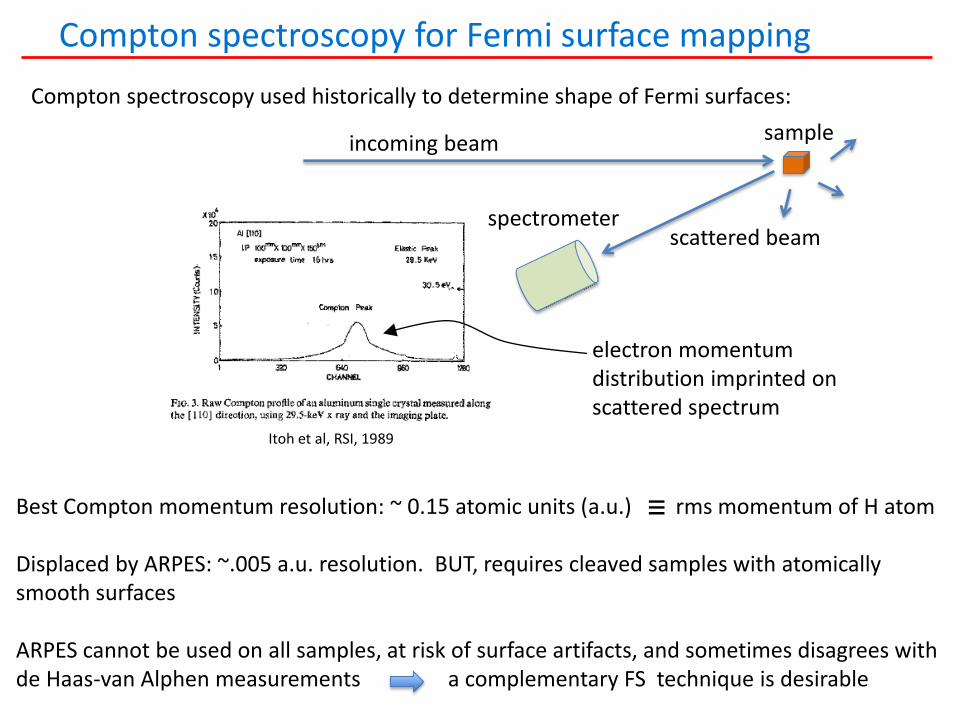
Compton spectroscopy for Fermi surface mapping
Compton spectroscopy used historically to determine shape of Fermi surfaces:
W Si
incoming beam
scattered beam spectrometer
sample
Itoh et al, RSI, 1989
electron momentum distribution imprinted on scattered spectrum
Best Compton momentum resolution: ~ 0.15 atomic units (a.u.) rms momentum of H atom Displaced by ARPES: ~.005 a.u. resolution. BUT, requires cleaved samples with atomically smooth surfaces ARPES cannot be used on all samples, at risk of surface artifacts, and sometimes disagrees with de Haas-van Alphen measurements a complementary FS technique is desirable
º

TES detectors for Compton spectroscopy • TES detectors can radically improve Compton spectroscopy
W Si
• Compton with TESs: better momentum resolution (.02 a. u.) and much shorter integration times
• Traditional appeal of Compton retained: bulk sensitive, can look at many materials in range of conditions: temperature, pressure, magnetic field, …
• Collaboration with Peter Abbamonte (UIUC/APS), Nino Miceli (APS), Arun Bansil, Bernardo Barbiellini-Amidei (Northeastern), Chi-Chang Kao, Tom Devereaux (Stanford) to do demonstration at APS; looking for support
(Initiated by Phil Platzman)
Spring-8 BL08W; state of the art Compton beamline TES array: each pixel gives Compton spectrum
existing array: comparable resolution, ~5000x higher efficiency could optimize for 7x better resolution (11 eV) >100x more efficient more simple
vs.
80 eV resolution
(see also Hiraoka et al, J. Synch. Rad. 2001)

Areas of scientific opportunity
1. X-ray science below 10 keV
2. Compton scattering near 100 keV 1. Time-resolved X-ray measurements at beamlines, and in the laboratory
W Si
Ultrafast (fs-ps) structural measurements
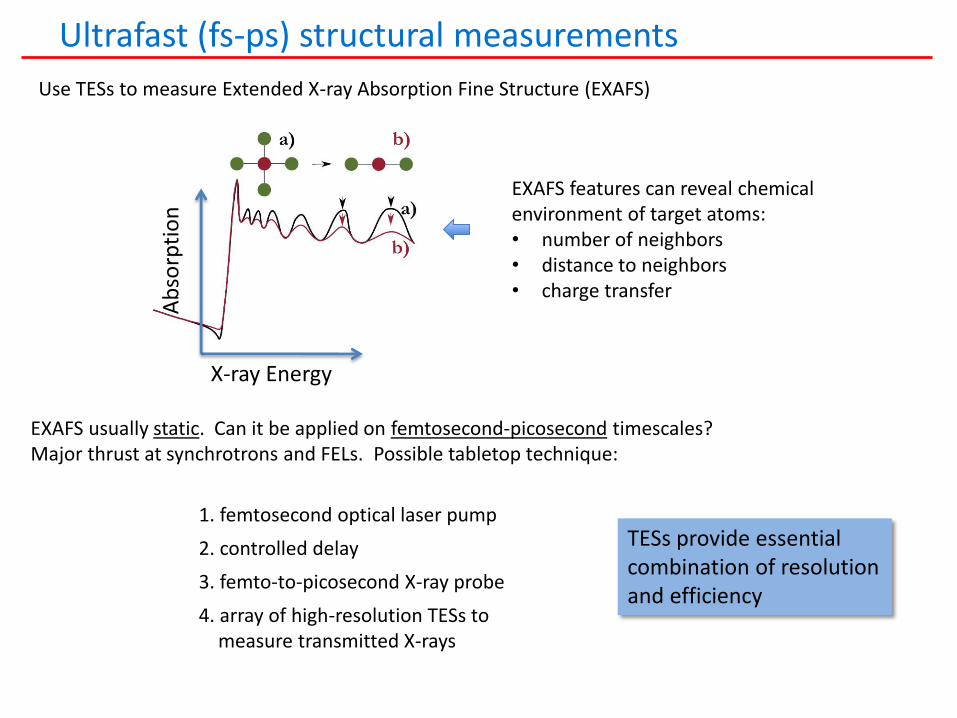
Use TESs to measure Extended X-ray Absorption Fine Structure (EXAFS)
X-ray Energy
Ab
sorp
tio
n
EXAFS usually static. Can it be applied on femtosecond-picosecond timescales? Major thrust at synchrotrons and FELs. Possible tabletop technique:
1. femtosecond optical laser pump
2. controlled delay
3. femto-to-picosecond X-ray probe
4. array of high-resolution TESs to measure transmitted X-rays
EXAFS features can reveal chemical environment of target atoms: • number of neighbors • distance to neighbors • charge transfer
TESs provide essential combination of resolution and efficiency

Top view
120 um water jet sample under study
optical pump beam
target chamber wall cryostat wall
Experimental schematic
Photoexcite sample
160 TES array

Top view
120 um water jet
target chamber wall cryostat wall
Photoexcite sample, then wait controlled delay
sample under study
Experimental schematic
160 TES array

Top view
120 um water jet
isotropic x-ray generation
focused probe beam
target chamber wall cryostat wall
160 TES array
sample under study
Generate X-ray pulse, measure transmitted spectrum
Experimental schematic

Top view
120 um water jet
isotropic x-ray generation
focused probe beam
target chamber wall cryostat wall
sample under study
Repeat pump-probe pulse pairs at same delay to accumulate statistics Then, change delay to build ‘molecular movie’ of EXAFS spectra with different delays after photoexcitation
Experimental schematic
160 TES array

Steps towards tabletop molecular movies
• Need <ps pulsed X-ray source: water jet laser plasma source
• We have delivered ucal spectrometer to Lund for initial demonstration:
First Extended X-ray Absorption Fine Structure (EXAFS) measurement with energy-dispersive detector correct Ferrocene bond length, but still static
Unpublished data removed
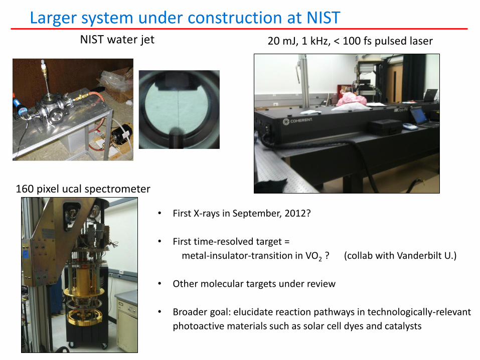
Larger system under construction at NIST 20 mJ, 1 kHz, < 100 fs pulsed laser
160 pixel ucal spectrometer
• First X-rays in September, 2012?
• First time-resolved target =
metal-insulator-transition in VO2 ? (collab with Vanderbilt U.)
• Other molecular targets under review
• Broader goal: elucidate reaction pathways in technologically-relevant
photoactive materials such as solar cell dyes and catalysts
Planned capability
• Compatible with thin-film samples or samples in solution
• Straightforward source range = ~ 2 – 10 keV - Covers K edges of S, Cl, Ar, K, Ca, Sc, Ti, V, Cr, Mn, Fe, Co, Ni, Cu, and Zn - Covers L edges from Rb to Er - Energies < 2 keV can be delivered with careful design and/or alternative source
• Array of 1024 pixels will provide ~ 500 useful photons/pulse
• Operation at 1 kHz 5e5 useful photons/sec
• To see a 0.1% intensity difference with 5σ precision, need 2.5e7 photons/bin
• Measure across 4 keV band with 5 eV bins 800 bins 2e10 photons
• Measurement time = 2e10 phos/5e5 pho/sec = 11 hrs for a very precise EXAFS
spectrum (in a tabletop experiment)
• Table top method as good as slicing beamlines
• High availability, disseminable; use as screening method for LCLS beamtime?

Research Needs
1. Proof-of-principle beamline experiments
2. Dedicated beamline spectrometers
3. Partnering with light source scientists on control and processing software
4. Large X-ray arrays (≥103 pixels) and associated readout:
It is realistic now to build a 103 pixel, 2 eV at 6 keV instrument.
Si
Most investment to date has come from other sponsors (NASA, DOE NNSA, NIST, NSF). Investment by DOE BES will accelerate experiments and technology that target BES goals.
Possible investment areas:

Transiton edge sensor summary slide
1. TESs have demonstrated excellent energy resolution:
- 1.3 eV FWHM at 1.5 keV, 1.6 eV at 6 keV, 22 eV at 97 keV
2. Arrays of 256 TES calorimeters exist now. 103 pixel arrays
realistic in 2-3 years. 106 pixel arrays in future.
3. A 103 pixel array can provide 100x or higher efficiency than
existing xtals and gratings below 10 keV. Good for older
beamlines, radiation sensitive samples, and time-resolved
measurements.
4. TES arrays will enable other applications such as improved
Compton scattering and table-top, ultrafast absorption
spectroscopy.
5. BES investment will speed progress. Likelihood of technical
success is high.
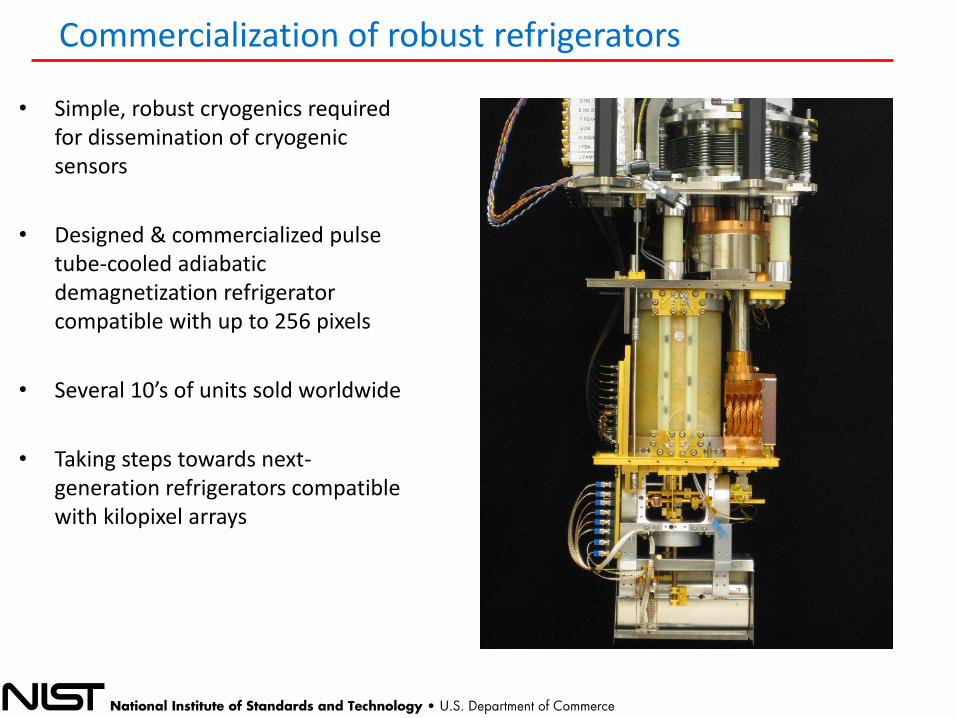
• Simple, robust cryogenics required for dissemination of cryogenic sensors
• Designed & commercialized pulse tube-cooled adiabatic demagnetization refrigerator compatible with up to 256 pixels
• Several 10’s of units sold worldwide
• Taking steps towards next-generation refrigerators compatible with kilopixel arrays
Commercialization of robust refrigerators
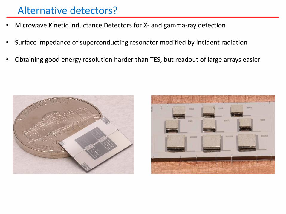
Alternative detectors? • Microwave Kinetic Inductance Detectors for X- and gamma-ray detection
• Surface impedance of superconducting resonator modified by incident radiation
• Obtaining good energy resolution harder than TES, but readout of large arrays easier

Improving industrial X-ray materials analysis • Polarization in the CMB
• Submillimeter astronomical imaging
• Submillimeter terrestrial imaging
• Single near-optical photon counting for quantum information
• Synchrotron X-ray science
• Industrial X-ray materials analysis
• Time-resolved X-ray absorption spectroscopy
• X-ray astronomy
• Gamma-ray nuclear materials analysis
• Gamma-ray astronomy
• Alpha-particle nuclear materials analysis
• Dark matter detection
• Electron beam-induced X-ray fluorescence is a ubiquitous tool for determining elemental composition on SEMs and TEMs
• TES X-ray detectors can provide ~ 50x better resolution than Silicon Drift detectors (SDDs)
• We have designed a SEM-mounted TES spectrometer. Now a commercial product for STAR Cryoelectronics.
Cryogen-free spectrometer with 16 TES X-ray array – STAR Cryoelectronics
• Industrial X-ray materials analysis