Embed Size (px)
DESCRIPTION
Transients and Step Responses. ELCT222- Lecture Notes University of S. Carolina Fall2011. Outline. RC transients charging RC transients discharge RC transients Thevenin P-SPICE RL transients charging RL transients discharge Step responses. P-SPICE simulations Applications. Reading: - PowerPoint PPT Presentation
Citation preview

TRANSIENTS AND STEP RESPONSESELCT222- Lecture Notes
University of S. Carolina
Fall2011

OUTLINE RC transients charging RC transients discharge RC transients Thevenin P-SPICE RL transients charging RL transients discharge Step responses. P-SPICE simulations Applications
Reading:Boylestad Sections10.5, 10.6, 10.7, 10.9,10.1024.1-24.7

TRANSIENTS IN CAPACITIVE NETWORKS: THE CHARGING PHASE
The placement of charge on the plates of a capacitor does not occur instantaneously.
Instead, it occurs over a period of time determined by the components of the network.
FIG. 10.26 Basic R-C charging network.

TRANSIENTS IN CAPACITIVE NETWORKS: THE CHARGING PHASE
FIG. 10.27 vC during the charging phase.

TRANSIENTS IN CAPACITIVE NETWORKS: THE CHARGING PHASE
FIG. 10.28 Universal time constant chart.
TRANSIENTS IN CAPACITIVE NETWORKS: THE CHARGING PHASE
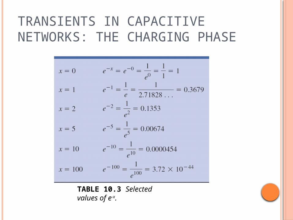
TABLE 10.3 Selected values of e-x.

TRANSIENTS IN CAPACITIVE NETWORKS: THE CHARGING PHASE
The factor t, called the time constant of the network, has the units of time, as shown below using some of the basic equations introduced earlier in this text:
The larger R is, the lower the charging current, longer time to chargeThe larger C is, the more charge required for a given V, longer time.

TRANSIENTS IN CAPACITIVE NETWORKS: THE CHARGING PHASE
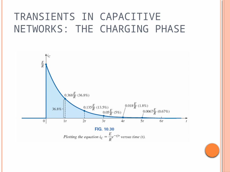
FIG. 10.29 Plotting the equation yC = E(1 – e-t/t) versus time (t).
TRANSIENTS IN CAPACITIVE NETWORKS: THE CHARGING PHASE

TRANSIENTS IN CAPACITIVE NETWORKS: THE CHARGING PHASE
FIG. 10.32 Revealing the short-circuit equivalent for the capacitor that occurs when the switch is first closed.

TRANSIENTS IN CAPACITIVE NETWORKS: THE CHARGING PHASE
FIG. 10.31 Demonstrating that a capacitor has the characteristics of an open circuit after the charging phase has passed.

TRANSIENTS IN CAPACITIVE NETWORKS: THE CHARGING PHASE
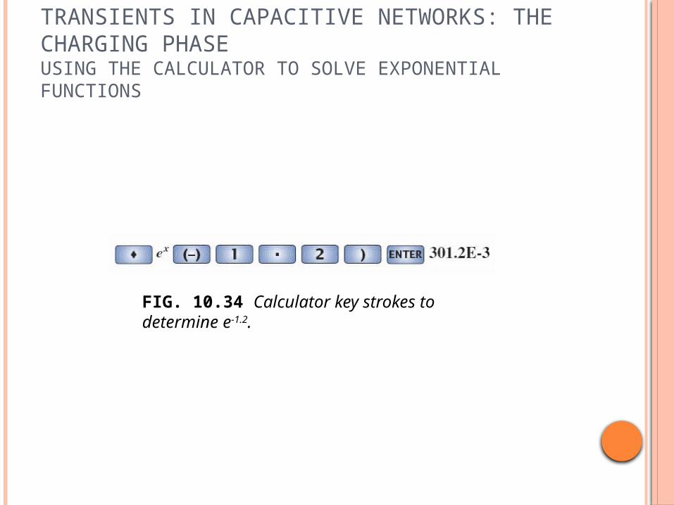
TRANSIENTS IN CAPACITIVE NETWORKS: THE CHARGING PHASEUSING THE CALCULATOR TO SOLVE EXPONENTIAL FUNCTIONS
FIG. 10.34 Calculator key strokes to determine e-1.2.

TRANSIENTS IN CAPACITIVE NETWORKS: THE CHARGING PHASEUSING THE CALCULATOR TO SOLVE EXPONENTIAL FUNCTIONS
FIG. 10.35 Transient network for Example 10.6.

TRANSIENTS IN CAPACITIVE NETWORKS: THE CHARGING PHASEUSING THE CALCULATOR TO SOLVE EXPONENTIAL FUNCTIONS
FIG. 10.36 vC versus time for the charging network in Fig. 10.35.

TRANSIENTS IN CAPACITIVE NETWORKS: THE CHARGING PHASEUSING THE CALCULATOR TO SOLVE EXPONENTIAL FUNCTIONS
FIG. 10.37 Plotting the waveform in Fig. 10.36 versus time (t).

TRANSIENTS IN CAPACITIVE NETWORKS: THE CHARGING PHASEUSING THE CALCULATOR TO SOLVE EXPONENTIAL FUNCTIONS
FIG. 10.38 iC and yR for the charging network in Fig. 10.36.

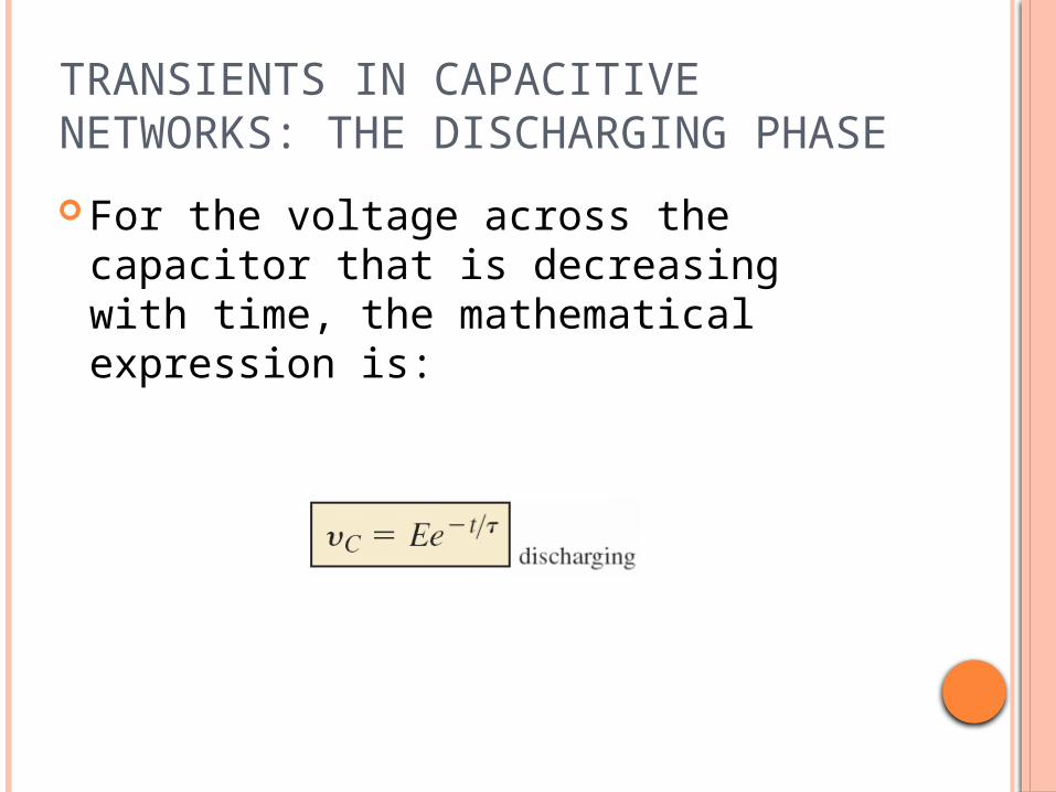
TRANSIENTS IN CAPACITIVE NETWORKS: THE DISCHARGING PHASE
We now investigate how to discharge a capacitor while exerting some control on how long the discharge time will be.
You can, of course, place a lead directly across a capacitor to discharge it very quickly—and possibly cause a visible spark.
For larger capacitors such those in TV sets, this procedure should not be attempted because of the high voltages involved—unless, of course, you are trained in the maneuver.

TRANSIENTS IN CAPACITIVE NETWORKS: THE DISCHARGING PHASE
FIG. 10.39 (a) Charging network; (b) discharging configuration.
TRANSIENTS IN CAPACITIVE NETWORKS: THE DISCHARGING PHASE
For the voltage across the capacitor that is decreasing with time, the mathematical expression is:

TRANSIENTS IN CAPACITIVE NETWORKS: THE DISCHARGING PHASE
FIG. 10.40 yC, iC, and yR for 5t switching between contacts in Fig. 10.39(a).
TRANSIENTS IN CAPACITIVE NETWORKS: THE DISCHARGING PHASE
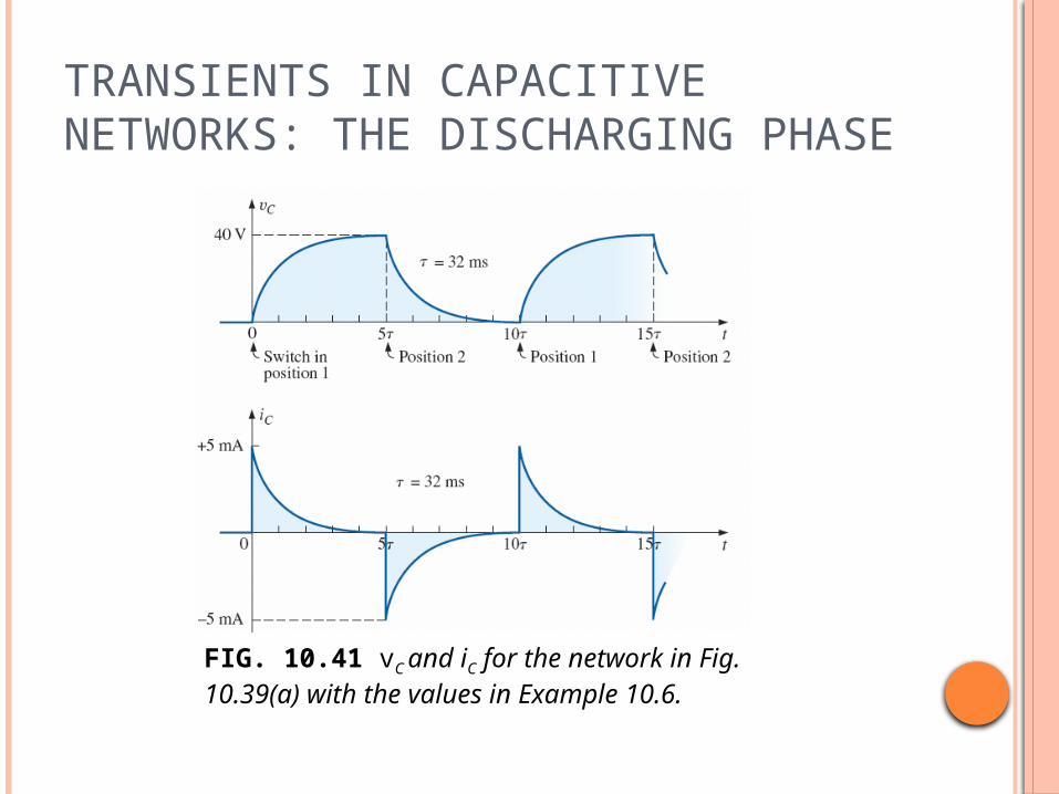
FIG. 10.41 vC and iC for the network in Fig. 10.39(a) with the values in Example 10.6.

TRANSIENTS IN CAPACITIVE NETWORKS: THE DISCHARGING PHASETHE EFFECT OF ON THE RESPONSE

TRANSIENTS IN CAPACITIVE NETWORKS: THE DISCHARGING PHASETHE EFFECT OF ON THE RESPONSE
FIG. 10.43 Effect of increasing values of C (with R constant) on the charging curve for vC.

TRANSIENTS IN CAPACITIVE NETWORKS: THE DISCHARGING PHASETHE EFFECT OF ON THE RESPONSE
FIG. 10.44 Network to be analyzed in Example 10.8.

TRANSIENTS IN CAPACITIVE NETWORKS: THE DISCHARGING PHASETHE EFFECT OF ON THE RESPONSE
FIG. 10.45 vC and iC for the network in Fig. 10.44.

TRANSIENTS IN CAPACITIVE NETWORKS: THE DISCHARGING PHASETHE EFFECT OF ON THE RESPONSE
FIG. 10.46 Network to be analyzed in Example 10.9.
FIG. 10.47 The charging phase for the network in Fig. 10.46.

TRANSIENTS IN CAPACITIVE NETWORKS: THE DISCHARGING PHASETHE EFFECT OF ON THE RESPONSE
FIG. 10.48 Network in Fig. 10.47 when the switch is moved to position 2 at t = 1t1.

TRANSIENTS IN CAPACITIVE NETWORKS: THE DISCHARGING PHASETHE EFFECT OF ON THE RESPONSE
FIG. 10.49 vC for the network in Fig. 10.47.

TRANSIENTS IN CAPACITIVE NETWORKS: THE DISCHARGING PHASETHE EFFECT OF ON THE RESPONSE
FIG. 10.50 ic for the network in Fig. 10.47.

INITIAL CONDITIONS The voltage across the capacitor at
this instant is called the initial value, as shown for the general waveform in Fig. 10.51.
FIG. 10.51 Defining the regions associated with a transient response.
vc =Vf + (Vi −Vf )e−t/τ

INITIAL CONDITIONS
FIG. 10.52 Example 10.10.

INITIAL CONDITIONS
FIG. 10.53 vC and iC for the network in Fig. 10.52.

INITIAL CONDITIONS
FIG. 10.54 Defining the parameters in Eq. (10.21) for the discharge phase.

INSTANTANEOUS VALUES
Occasionally, you may need to determine the voltage or current at a particular instant of time that is not an integral multiple of t.
FIG. 10.55 Key strokes to determine (2 ms)(loge2) using the TI-89 calculator.

THÉVENIN EQUIVALENT: T =RTHC
You may encounter instances in which the network does not have the simple series form in Fig. 10.26.
You then need to find the Thévenin equivalent circuit for the network external to the capacitive element.

THÉVENIN EQUIVALENT: T =RTHC
FIG. 10.56 Example 10.11.

THÉVENIN EQUIVALENT: T =RTHC
FIG. 10.57 Applying Thévenin’s theorem to the network in Fig. 10.56.

THÉVENIN EQUIVALENT: T =RTHC
FIG. 10.58 Substituting the Thévenin equivalent for the network in Fig. 10.56.

THÉVENIN EQUIVALENT: T =RTHC
FIG. 10.59 The resulting waveforms for the network in Fig. 10.56.

THÉVENIN EQUIVALENT: T =RTHC
FIG. 10.60 Example 10.12.
FIG. 10.61 Network in Fig. 10.60 redrawn.

THÉVENIN EQUIVALENT: T =RTHC
FIG. 10.62 yC for the network in Fig. 10.60.

THÉVENIN EQUIVALENT: T =RTHC
FIG. 10.63 Example 10.13.
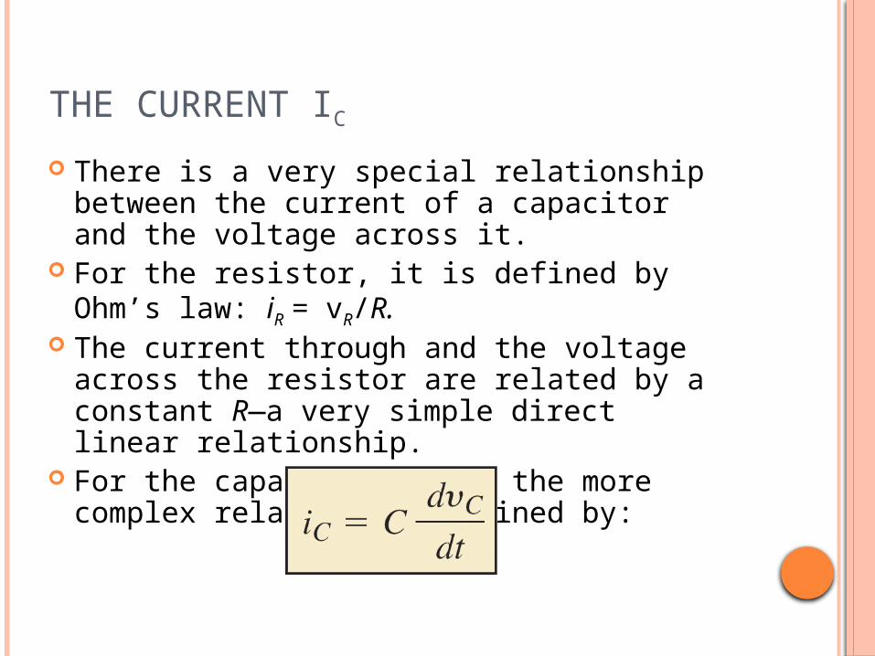
THE CURRENT IC There is a very special relationship between
the current of a capacitor and the voltage across it.
For the resistor, it is defined by Ohm’s law: iR = vR/R.
The current through and the voltage across the resistor are related by a constant R—a very simple direct linear relationship.
For the capacitor, it is the more complex relationship defined by:

THE CURRENT IC
FIG. 10.64 vC for Example 10.14.

THE CURRENT IC
FIG. 10.65 The resulting current iC for the applied voltage in Fig. 10.64.

INDUCTORS

R-L TRANSIENTS: THE STORAGE PHASE
The storage waveforms have the same shape, and time constants are defined for each configuration.
Because these concepts are so similar (refer to Section 10.5 on the charging of a capacitor), you have an opportunity to reinforce concepts introduced earlier and still learn more about the behavior of inductive elements.

R-L TRANSIENTS: THE STORAGE PHASE
FIG. 11.31 Basic R-L transient network.
Remember, for an inductor vL =LdiLdt

R-L TRANSIENTS: THE STORAGE PHASE
FIG. 11.32 iL, yL, and yR for the circuit in Fig. 11.31 following the closing of the switch.

R-L TRANSIENTS: THE STORAGE PHASE
FIG. 11.33 Effect of L on the shape of the iL storage waveform.

R-L TRANSIENTS: THE STORAGE PHASE
FIG. 11.34 Circuit in Figure 11.31 the instant the switch is closed.

R-L TRANSIENTS: THE STORAGE PHASE
FIG. 11.35 Circuit in Fig. 11.31 under steady-state conditions.
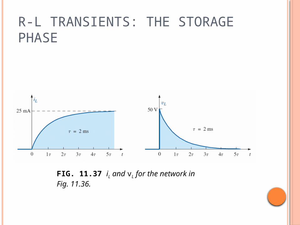
FIG. 11.36 Series R-L circuit for Example 11.3.
R-L TRANSIENTS: THE STORAGE PHASE
FIG. 11.37 iL and vL for the network in Fig. 11.36.

INITIAL CONDITIONS Since the current through a coil cannot
change instantaneously, the current through a coil begins the transient phase at the initial value established by the network (note Fig. 11.38) before the switch was closed.
It then passes through the transient phase until it reaches the steady-state (or final) level after about five time constants.
The steadystate level of the inductor current can be found by substituting its shortcircuit equivalent (or Rl for the practical equivalent) and finding the resulting current through the element.

INITIAL CONDITIONS
FIG. 11.38 Defining the three phases of a transient waveform.

INITIAL CONDITIONS
FIG. 11.39 Example 11.4.

INITIAL CONDITIONS
FIG. 11.40 iL and vL for the network in Fig. 11.39.

R-L TRANSIENTS: THE RELEASE PHASE
FIG. 11.41 Demonstrating the effect of opening a switch in series with an inductor with a steady-state current.

R-L TRANSIENTS: THE RELEASE PHASE
FIG. 11.42 Initiating the storage phase for an inductor by closing the switch.

R-L TRANSIENTS: THE RELEASE PHASE
FIG. 11.43 Network in Fig. 11.42 the instant the switch is opened.

R-L TRANSIENTS: THE RELEASE PHASE

R-L TRANSIENTS: THE RELEASE PHASE
FIG. 11.45 The various voltages and the current for the network in Fig. 11.44.

STEP RESPONSES

OBJECTIVES Become familiar with the specific terms that
define a pulse waveform and how to calculate various parameters such as the pulse width, rise and fall times, and tilt.
Be able to calculate the pulse repetition rate and the duty cycle of any pulse waveform.
Become aware of the parameters that define the response of an R-C network to a square-wave input.
Understand how a compensator probe of an oscilloscope is used to improve the appearance of an output pulse waveform.

IDEAL VERSUS ACTUAL
The ideal pulse in Fig. 24.1 has vertical sides, sharp corners, and a flat peak characteristic; it starts instantaneously at t1 and ends just as abruptly at t2.
FIG. 24.1 Ideal pulse waveform.

IDEAL VERSUS ACTUAL
FIG. 24.2 Actual pulse waveform.

IDEAL VERSUS ACTUAL
Amplitude Pulse Width Base-Line Voltage Positive-Going and Negative-Going
Pulses Rise Time (tr) and Fall Time (tf) Tilt

IDEAL VERSUS ACTUAL
FIG. 24.3 Defining the base-line voltage.

IDEAL VERSUS ACTUAL
FIG. 24.4 Positive-going pulse.

IDEAL VERSUS ACTUAL
FIG. 24.5 Defining tr and tf.

IDEAL VERSUS ACTUAL
FIG. 24.6 Defining tilt.

IDEAL VERSUS ACTUAL
FIG. 24.7 Defining preshoot, overshoot, and ringing.

IDEAL VERSUS ACTUAL
FIG. 24.8 Example 24.1.

IDEAL VERSUS ACTUAL
FIG. 24.9 Example 24.2.

PULSE REPETITION RATE AND DUTY CYCLE
A series of pulses such as those appearing in Fig. 24.10 is called a pulse train.
The varying widths and heights may contain information that can be decoded at the receiving end.
If the pattern repeats itself in a periodic manner as shown in Fig. 24.11(a) and (b), the result is called a periodic pulse train.

PULSE REPETITION RATE AND DUTY CYCLE
FIG. 24.10 Pulse train.

PULSE REPETITION RATE AND DUTY CYCLE
FIG. 24.11 Periodic pulse trains.

PULSE REPETITION RATE AND DUTY CYCLE
FIG. 24.12 Example 24.3.

PULSE REPETITION RATE AND DUTY CYCLE
FIG. 24.13 Example 24.4.

PULSE REPETITION RATE AND DUTY CYCLE
FIG. 24.14 Example 24.5.

AVERAGE VALUE
The average value of a pulse waveform can be determined using one of two methods.
The first is the procedure outlined in Section 13.7, which can be applied to any alternating waveform.
The second can be applied only to pulse waveforms since it utilizes terms specifically related to pulse waveforms; that is,

AVERAGE VALUE
FIG. 24.15 Example 24.6.
AVERAGE VALUE
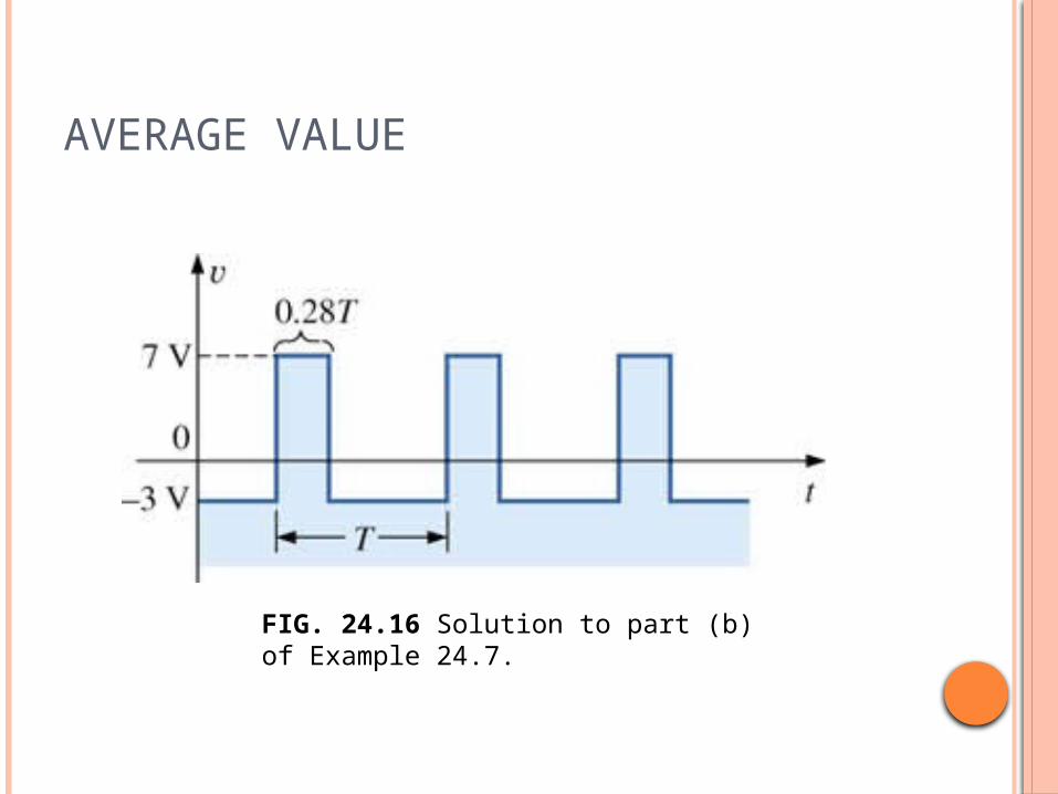
FIG. 24.16 Solution to part (b) of Example 24.7.

AVERAGE VALUEINSTRUMENTATION The average value
(dc value) of any waveform can be easily determined using the oscilloscope.
If the mode switch of the scope is set in the ac position, the average or dc component of the applied waveform is blocked by an internal capacitor from reaching the screen.
FIG. 24.17 Determining the average value of a pulse waveform using an oscilloscope.

TRANSIENT R-C NETWORKS
In Chapter 10, the general solution for the transient behavior of an R-C network with or without initial values was developed.
The resulting equation for the voltage across a capacitor is repeated here for convenience:

TRANSIENT R-C NETWORKS
FIG. 24.18 Defining the parameters of Eq. (24.6).

TRANSIENT R-C NETWORKS
FIG. 24.19 Example of the use of Eq. (24.6).
TRANSIENT R-C NETWORKS
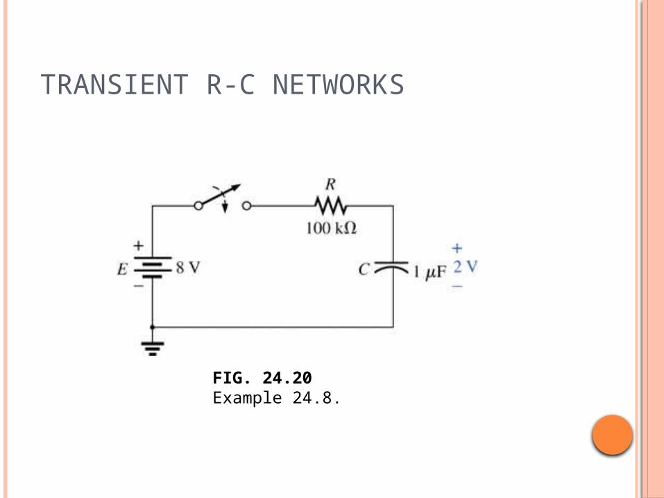
FIG. 24.20 Example 24.8.

TRANSIENT R-C NETWORKS
FIG. 24.21 yC and iC for the network in Fig. 24.20.

TRANSIENT R-C NETWORKS
FIG. 24.22 Example 24.9.

TRANSIENT R-C NETWORKS
FIG. 24.23 vC for the network in Fig. 24.22.

R-C RESPONSE TO SQUARE-WAVE INPUTS The square wave in Fig. 24.24 is a
particular form of pulse waveform. It has a duty cycle of 50% and an
average value of zero volts, as calculated as follows:
FIG. 24.24 Periodic square wave.

R-C RESPONSE TO SQUARE-WAVE INPUTS
FIG. 24.25 Raising the base-line voltage of a square wave to zero volts.

R-C RESPONSE TO SQUARE-WAVE INPUTS
FIG. 24.26 Applying a periodic square-wave pulse train to an R-C network.

T/2 > 5T

T/2 = 5T

T/2 < 5T

T/2 < 5T
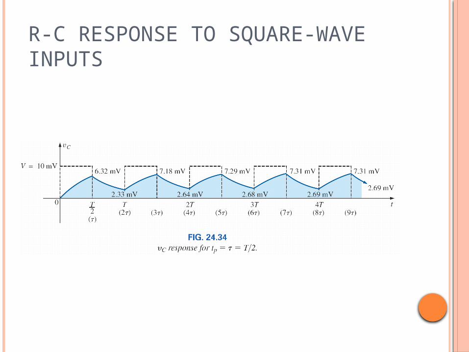
FIG. 24.30 vC for T/2 << 5t or T << 10t.

R-C RESPONSE TO SQUARE-WAVE INPUTS
FIG. 24.31 Example 24.10.

R-C RESPONSE TO SQUARE-WAVE INPUTS
FIG. 24.32 vC for the R-C network in Fig. 24.31.

R-C RESPONSE TO SQUARE-WAVE INPUTS
FIG. 24.33 iC for the R-C network in Fig. 24.31.
R-C RESPONSE TO SQUARE-WAVE INPUTS

R-C RESPONSE TO SQUARE-WAVE INPUTS

OSCILLOSCOPE ATTENUATOR AND COMPENSATING PROBE The X10 attenuator probe used with
oscilloscopes is designed to reduce the magnitude of the input voltage by a factor of 10.
If the input impedance to a scope is 1 MΩ, the X10 attenuator probe will have an internal resistance of 9 MΩ, as shown in Fig. 24.36.