Embed Size (px)
Citation preview
TPS65981, TPS65982, and TPS65986 FirmwareUser’s Guide
User's Guide
Literature Number: SLVUAH7BJune 2015–Revised July 2016
2 SLVUAH7B–June 2015–Revised July 2016Submit Documentation Feedback
Copyright © 2015–2016, Texas Instruments Incorporated
Contents
Contents
1 Introduction......................................................................................................................... 51.1 Purpose and Scope ......................................................................................................... 51.2 Related Documents.......................................................................................................... 5
2 Overview............................................................................................................................. 62.1 TPS65982 versus TPS65986 .............................................................................................. 62.2 TPS65982 versus TPS65981 .............................................................................................. 6
3 Boot Code ........................................................................................................................... 73.1 Boot Code .................................................................................................................... 73.2 Initialization ................................................................................................................... 83.3 I2C Configuration ............................................................................................................. 83.4 Dead Battery ................................................................................................................. 93.5 Application Code ........................................................................................................... 103.6 Flash Memory Read ....................................................................................................... 113.7 Invalid Flash Memory ...................................................................................................... 123.8 UART Download............................................................................................................ 13
4 Application Code................................................................................................................ 154.1 Overview..................................................................................................................... 154.2 Application Code Boot Header ........................................................................................... 154.3 I2C Host Interface........................................................................................................... 154.4 Updating Application Code................................................................................................ 15
4.4.1 Application Code Update through I2C........................................................................... 164.4.2 Application Code Update through External Device ........................................................... 17
5 Power Management ............................................................................................................ 185.1 Power States................................................................................................................ 185.2 Activity Timer................................................................................................................ 195.3 System Power State ....................................................................................................... 195.4 Power State Descriptions ................................................................................................. 19
5.4.1 POWER OFF ...................................................................................................... 195.4.2 RESET.............................................................................................................. 195.4.3 SLEEP .............................................................................................................. 195.4.4 IDLE................................................................................................................. 205.4.5 ACTIVE ............................................................................................................. 215.4.6 Dead Battery ....................................................................................................... 21
6 USB Type-C ....................................................................................................................... 236.1 Overview..................................................................................................................... 236.2 USB Type-C Port Configuration .......................................................................................... 23
6.2.1 Source .............................................................................................................. 236.2.2 Sink.................................................................................................................. 23
6.3 CC Detection................................................................................................................ 246.4 USB Type-C Connection State Machine ................................................................................ 24
7 Accessory Modes ............................................................................................................... 257.1 Audio Accessory Mode .................................................................................................... 257.2 Debug Accessory Mode ................................................................................................... 25
8 Type-C Port Multiplexer Configurations ................................................................................ 26
www.ti.com
3SLVUAH7B–June 2015–Revised July 2016Submit Documentation Feedback
Copyright © 2015–2016, Texas Instruments Incorporated
Contents
9 USB Power Delivery............................................................................................................ 279.1 Overview..................................................................................................................... 279.2 Protocol Layer .............................................................................................................. 27
9.2.1 Control Messages ................................................................................................. 279.2.2 Data Messages .................................................................................................... 289.2.3 Reset................................................................................................................ 28
9.3 Policy Engine ............................................................................................................... 289.3.1 Request Message ................................................................................................. 29
10 Alternate Modes ................................................................................................................. 3010.1 Overview..................................................................................................................... 3010.2 USB Billboard ............................................................................................................... 3010.3 Automatic Entry............................................................................................................. 3010.4 DisplayPort Alternate Mode ............................................................................................... 3010.5 PDIO Alternate Mode ...................................................................................................... 31
10.5.1 Overview .......................................................................................................... 3110.5.2 PDIO GPIO Events .............................................................................................. 3210.5.3 PDIO Signature................................................................................................... 32
10.6 User Alternate Mode ....................................................................................................... 3210.6.1 Enter the Alternate Mode........................................................................................ 3210.6.2 Send Unstructured Vendor-Defined Message................................................................ 3310.6.3 Reconfigure the TPS65982 from Data Set ................................................................... 3310.6.4 Execute Host-Interface Commands............................................................................ 33
11 Power Delivery Fault Handling ............................................................................................. 3412 Charger Detection .............................................................................................................. 35
12.1 Firmware Description ...................................................................................................... 3512.1.1 VBUS Detect...................................................................................................... 3512.1.2 Data-Contact Detect ............................................................................................. 3612.1.3 Primary Detection ................................................................................................ 3612.1.4 Secondary Detection............................................................................................. 37
13 Device Features ................................................................................................................. 3813.1 ADC .......................................................................................................................... 3813.2 Digital I/O .................................................................................................................... 3813.3 Load App Config Set GPIO Events ...................................................................................... 41
Revision History.......................................................................................................................... 42
www.ti.com
4 SLVUAH7B–June 2015–Revised July 2016Submit Documentation Feedback
Copyright © 2015–2016, Texas Instruments Incorporated
List of Figures
List of Figures3-1. Boot-Code Sequence ....................................................................................................... 83-2. I2C Address Configuration .................................................................................................. 93-3. Dead-Battery Process ..................................................................................................... 103-4. TPS65982 Flash-Memory Organization ................................................................................. 113-5. Flash Read Flow ........................................................................................................... 123-6. Memory Invalid Flow ....................................................................................................... 133-7. UART Download Process ................................................................................................. 145-1. Power State Diagram ...................................................................................................... 1810-1. DisplayPort Sink-Side Hardware Flow (HPD RX)...................................................................... 3110-2. DisplayPort Sink-Side Firmware Flow (HPD RX) ...................................................................... 3110-3. PDIO Alternate Mode ...................................................................................................... 3112-1. Charger-Detection State Machine........................................................................................ 3512-2. Data-Contact Detect (DCD) ............................................................................................... 3612-3. Primary Detection .......................................................................................................... 3712-4. Secondary Detection....................................................................................................... 37
List of Tables4-1. Application Code Structure................................................................................................ 155-1. Power States Summary ................................................................................................... 186-1. USB Type-C Port State Based on CC Terminations (Source Perspective) ........................................ 246-2. USB Type-C Connection States Supported ............................................................................ 248-1. USB Type-C Port Multiplexer Configurations........................................................................... 269-1. Control Messages .......................................................................................................... 279-2. USB PD Message Sequences Supported by the TPS65982......................................................... 2810-1. PDIO Signature ............................................................................................................. 3211-1. Power Delivery Fault Conditions ......................................................................................... 3413-1. GPIO Events ................................................................................................................ 39
5SLVUAH7B–June 2015–Revised July 2016Submit Documentation Feedback
Copyright © 2015–2016, Texas Instruments Incorporated
Introduction
Chapter 1SLVUAH7B–June 2015–Revised July 2016
Introduction
1.1 Purpose and ScopeThis document is the Firmware User’s Guide for the TPS65981, TPS65982, and TPS65986 USB Type-Cand USB Power Delivery (PD) controller, power switch, and high-speed multiplexer. The firmware for theTPS65981, TPS65982, and TPS65986 devices controls the port state, negotiates port-power levels, andallows for the entry and configuration of various alternate modes. These behaviors can be configuredusing the TPS6598x Configuration Tool.
This document intends to complement the standard specifications. Texas Instruments recommends to usethe user’s guide in conjunction with those standard specifications. If a conflict exists between this user’sguide and any of the standard specifications, the standard specifications are to be referenced.
Similarly, despite selective inclusions from the TPS65982 device specification for the same reasonsmentioned previously, the detailed description of the hardware features of TPS65982 device is beyond thescope of this user’s guide and the TPS65982 data sheet, TPS65982 USB Type-C and USB PD Controller,Power Switch, and High Speed Multiplexer, must be referenced.
1.2 Related Documents• TPS65982 USB Type-C and USB PD Controller, Power Switch, and High Speed Multiplexer• TPS65986 USB Type-C and USB PD Controller and Power Switch• TPS65981 USB Type-C and USB PD Controller, Power Switch, and High Speed Multiplexer• TPS65981, TPS65982, and TPS65986 Host Interface Technical Reference Manual• Battery Charging Specification, Revision 1.2, December 7, 2010 plus Errata.• DisplayPort Alt Mode Plug Requirement Corrections and Protocol Clarifications• Universal Serial Bus 3.1 Specification, Revision 1.0, July 26, 2013 plus ECN and Errata.
www.usb.org/developers/docs• Universal Serial Bus Power Delivery Specification, Revision 2.0, V1.1, May 7, 2015.
www.usb.org/developers/docs• Universal Serial Bus Specification, Revision 2.0, April 27, 2000 plus ECN and Errata.
http://www.usb.org/developers/docs/usb20_docs/• Universal Serial Bus Type-C Cable and Connector Specification, Revision 1.1, April 3, 2015.
www.usb.org/developers/docs• VESA DisplayPort (DP) Standard, Version 1.3, September 17, 2014.• VESA DisplayPort Alt Mode on USB Type-C Standard, Version 1.0, September 22, 2014.
6 SLVUAH7B–June 2015–Revised July 2016Submit Documentation Feedback
Copyright © 2015–2016, Texas Instruments Incorporated
Overview
Chapter 2SLVUAH7B–June 2015–Revised July 2016
Overview
The TPS65982 firmware is responsible for controlling the various analog and digital components of theTPS65982 device. The TPS65982 firmware is divided into two sections: boot code and application code.The boot code is responsible for configuration of the device immediately after power application. The bootcode is stored on internal device memory and cannot be altered. The TPS65982 application code is storedexternally, and is loaded by the boot code. When the application code is loaded, this section of firmware isresponsible for implementing the various required functionality for a USB Type-C device.
The TPS65982 device is the most integrated of the three devices (TPS65981, TPS65982, and TPS65986)that share the same core firmware. Because of the fact that the TPS65982 hardware contains all featuresthat can be controlled by the firmware, the behavior of the firmware is commonly described by referring tothe TPS65982 device only although it may also apply to the TPS65981, TPS65986, or both device.
2.1 TPS65982 versus TPS65986Both the TPS65982 and TPS65986 devices are capable of controlling a USB Type-C port; however, theTPS65986 device does not contain the proper hardware for controlling an external power path oroperating the Thunderbolt alternate mode. As such, any firmware behaviors or controls related to thesefeatures are not available on firmware offered for the TPS65986 device. The TPS65986 templates in theTPS6598x Configuration Tool accurately reflect the configurable parameters available for this device. Fordetails on the pin-out of the TPS65986 device, refer to the TPS65986 data sheet, TPS65986 USB Type-Cand USB PD Controller and Power Switch.
2.2 TPS65982 versus TPS65981Both the TPS65982 and TPS65981 devices are capable of controlling a USB Type-C port; however, theTPS65981 device does not contain the proper hardware for operating the Thunderbolt alternate mode orallow two or more devices to share a single SPI flash IC. In addition, the TPS65981 device has four lessGPIO pins and does not have an I2C_ADDR pin for setting the three least significant bits of the I2C slaveaddress. As such, any firmware behaviors or controls related to these features are not available onfirmware offered for the TPS65981 device. The TPS65981 templates in the TPS6598x Configuration Toolaccurately reflect the configurable parameters available for this device. For details on the pin-out of theTPS65981, refer to the TPS65981 Data sheet, TPS65981 USB Type-C and USB PD Controller, PowerSwitch, and High Speed Multiplexer.
7SLVUAH7B–June 2015–Revised July 2016Submit Documentation Feedback
Copyright © 2015–2016, Texas Instruments Incorporated
Boot Code
Chapter 3SLVUAH7B–June 2015–Revised July 2016
Boot Code
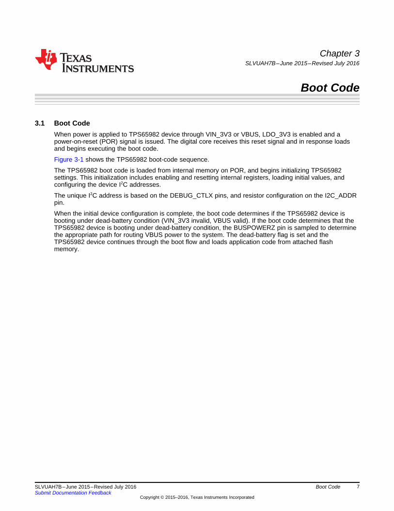
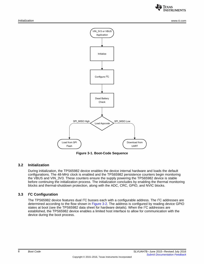
3.1 Boot CodeWhen power is applied to TPS65982 device through VIN_3V3 or VBUS, LDO_3V3 is enabled and apower-on-reset (POR) signal is issued. The digital core receives this reset signal and in response loadsand begins executing the boot code.
Figure 3-1 shows the TPS65982 boot-code sequence.
The TPS65982 boot code is loaded from internal memory on POR, and begins initializing TPS65982settings. This initialization includes enabling and resetting internal registers, loading initial values, andconfiguring the device I2C addresses.
The unique I2C address is based on the DEBUG_CTLX pins, and resistor configuration on the I2C_ADDRpin.
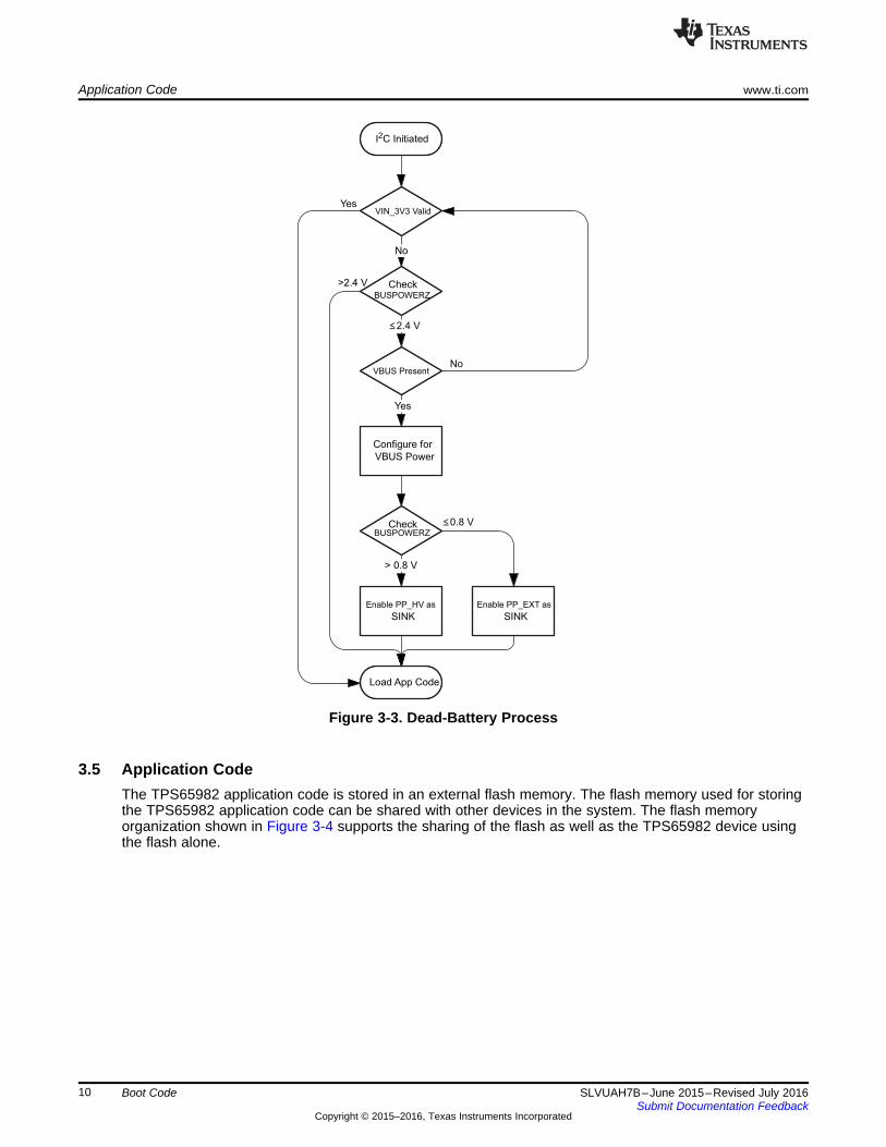
When the initial device configuration is complete, the boot code determines if the TPS65982 device isbooting under dead-battery condition (VIN_3V3 invalid, VBUS valid). If the boot code determines that theTPS65982 device is booting under dead-battery condition, the BUSPOWERZ pin is sampled to determinethe appropriate path for routing VBUS power to the system. The dead-battery flag is set and theTPS65982 device continues through the boot flow and loads application code from attached flashmemory.
VIN_3V3 or VBUS
Application
Initialize
Configure I C2
Dead Battery
Check
Load Appcode
Load from SPI
Flash
Download from
UART
SPI_MISO High SPI_MISO Low
Initialization www.ti.com
8 SLVUAH7B–June 2015–Revised July 2016Submit Documentation Feedback
Copyright © 2015–2016, Texas Instruments Incorporated
Boot Code
Figure 3-1. Boot-Code Sequence
3.2 InitializationDuring initialization, the TPS65982 device enables the device internal hardware and loads the defaultconfigurations. The 48-MHz clock is enabled and the TPS65982 persistence counters begin monitoringthe VBUS and VIN_3V3. These counters ensure the supply powering the TPS65982 device is stablebefore continuing the initialization process. The initialization concludes by enabling the thermal monitoringblocks and thermal-shutdown protection, along with the ADC, CRC, GPIO, and NVIC blocks.
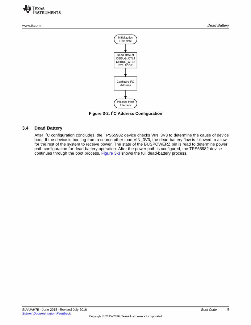
3.3 I2C ConfigurationThe TPS65982 device features dual I2C busses each with a configurable address. The I2C addresses aredetermined according to the flow shown in Figure 3-2. The address is configured by reading device GPIOstates at boot (see the TPS65982 data sheet for hardware details). When the I2C addresses areestablished, the TPS65982 device enables a limited host interface to allow for communication with thedevice during the boot process.
Read state of
DEBUG_CTL1
DEBUG_CTL2
I2C_ADDR
Configure I C2
Address
Initialize Host
Interface
Initialization
Complete
www.ti.com Dead Battery
9SLVUAH7B–June 2015–Revised July 2016Submit Documentation Feedback
Copyright © 2015–2016, Texas Instruments Incorporated
Boot Code
Figure 3-2. I2C Address Configuration
3.4 Dead BatteryAfter I2C configuration concludes, the TPS65982 device checks VIN_3V3 to determine the cause of deviceboot. If the device is booting from a source other than VIN_3V3, the dead-battery flow is followed to allowfor the rest of the system to receive power. The state of the BUSPOWERZ pin is read to determine powerpath configuration for dead-battery operation. After the power path is configured, the TPS65982 devicecontinues through the boot process. Figure 3-3 shows the full dead-battery process.
VIN_3V3 Valid
CheckBUSPOWERZ
VBUS Present
Configure for
VBUS Power
CheckBUSPOWERZ
Enable PP_HV as
SINK
Enable PP_EXT as
SINK
No
≤2.4 V
Yes
Load App Code
No
Yes
>2.4 V
I C Initiated2
≤0.8 V
> 0.8 V
Application Code www.ti.com
10 SLVUAH7B–June 2015–Revised July 2016Submit Documentation Feedback
Copyright © 2015–2016, Texas Instruments Incorporated
Boot Code
Figure 3-3. Dead-Battery Process
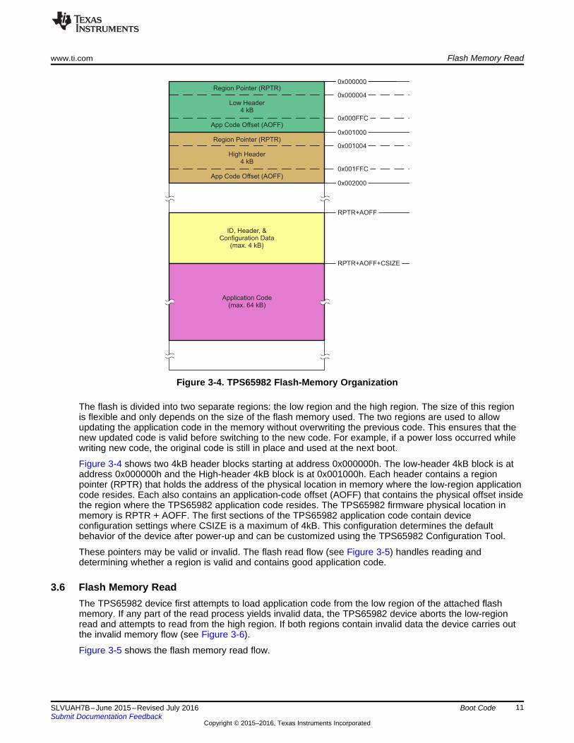
3.5 Application CodeThe TPS65982 application code is stored in an external flash memory. The flash memory used for storingthe TPS65982 application code can be shared with other devices in the system. The flash memoryorganization shown in Figure 3-4 supports the sharing of the flash as well as the TPS65982 device usingthe flash alone.
Region Pointer (RPTR)
Low Header4 kB
App Code Offset (AOFF)
Region Pointer (RPTR)
High Header4 kB
App Code Offset (AOFF)
0x000000
0x000004
0x000000
0x000FFC
0x001000
0x001004
0x001FFC
0x002000
RPTR+AOFF
RPTR+AOFF+CSIZE
Application Code(max. 64 kB)
ID, Header, &Configuration Data
(max. 4 kB)
www.ti.com Flash Memory Read
11SLVUAH7B–June 2015–Revised July 2016Submit Documentation Feedback
Copyright © 2015–2016, Texas Instruments Incorporated
Boot Code
Figure 3-4. TPS65982 Flash-Memory Organization
The flash is divided into two separate regions: the low region and the high region. The size of this regionis flexible and only depends on the size of the flash memory used. The two regions are used to allowupdating the application code in the memory without overwriting the previous code. This ensures that thenew updated code is valid before switching to the new code. For example, if a power loss occurred whilewriting new code, the original code is still in place and used at the next boot.
Figure 3-4 shows two 4kB header blocks starting at address 0x000000h. The low-header 4kB block is ataddress 0x000000h and the High-header 4kB block is at 0x001000h. Each header contains a regionpointer (RPTR) that holds the address of the physical location in memory where the low-region applicationcode resides. Each also contains an application-code offset (AOFF) that contains the physical offset insidethe region where the TPS65982 application code resides. The TPS65982 firmware physical location inmemory is RPTR + AOFF. The first sections of the TPS65982 application code contain deviceconfiguration settings where CSIZE is a maximum of 4kB. This configuration determines the defaultbehavior of the device after power-up and can be customized using the TPS65982 Configuration Tool.
These pointers may be valid or invalid. The flash read flow (see Figure 3-5) handles reading anddetermining whether a region is valid and contains good application code.
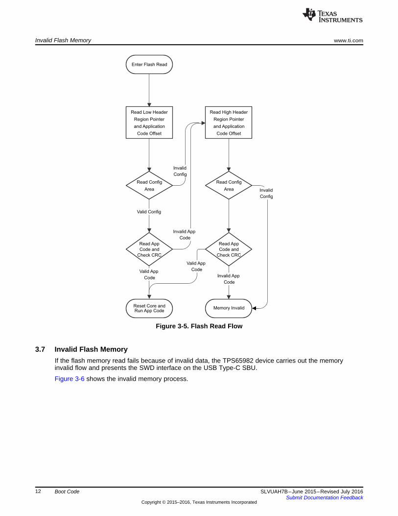
3.6 Flash Memory ReadThe TPS65982 device first attempts to load application code from the low region of the attached flashmemory. If any part of the read process yields invalid data, the TPS65982 device aborts the low-regionread and attempts to read from the high region. If both regions contain invalid data the device carries outthe invalid memory flow (see Figure 3-6).
Figure 3-5 shows the flash memory read flow.
Enter Flash Read
Read Low Header
Region Pointer
and Application
Code Offset
Read Config
Area
Read App
Code and
Check CRC
Reset Core andRun App Code
Read High Header
Region Pointer
and Application
Code Offset
Read Config
Area
Read App
Code and
Check CRC
Memory Invalid
Valid Config
Valid App
Code
Invalid
Config
Invalid App
Code
Invalid App
Code
Invalid
Config
Valid App
Code
Invalid Flash Memory www.ti.com
12 SLVUAH7B–June 2015–Revised July 2016Submit Documentation Feedback
Copyright © 2015–2016, Texas Instruments Incorporated
Boot Code
Figure 3-5. Flash Read Flow
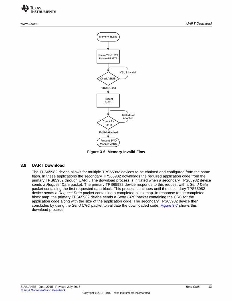
3.7 Invalid Flash MemoryIf the flash memory read fails because of invalid data, the TPS65982 device carries out the memoryinvalid flow and presents the SWD interface on the USB Type-C SBU.
Figure 3-6 shows the invalid memory process.
Memory Invalid
Enable VOUT_3V3
Release RESETZ
Check VBUS
Present
Rp/Rp
Check for
Rd/Rd
Present SWD
Monitor VBUS
VBUS Good
Rd/Rd Attached
VBUS Invalid
Rd/Rd Not
Attached
www.ti.com UART Download
13SLVUAH7B–June 2015–Revised July 2016Submit Documentation Feedback
Copyright © 2015–2016, Texas Instruments Incorporated
Boot Code
Figure 3-6. Memory Invalid Flow
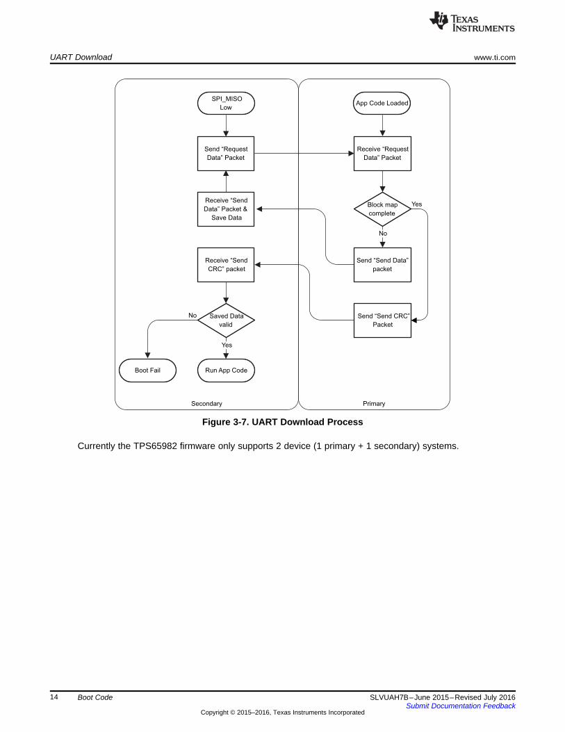
3.8 UART DownloadThe TPS65982 device allows for multiple TPS65982 devices to be chained and configured from the sameflash. In these applications the secondary TPS65982 downloads the required application code from theprimary TPS65982 through UART. The download process is initiated when a secondary TPS65982 devicesends a Request Data packet. The primary TPS65982 device responds to this request with a Send Datapacket containing the first requested data block. This process continues until the secondary TPS65982device sends a Request Data packet containing a completed block map. In response to the completedblock map, the primary TPS65982 device sends a Send CRC packet containing the CRC for theapplication code along with the size of the application code. The secondary TPS65982 device thenconcludes by using the Send CRC packet to validate the downloaded code. Figure 3-7 shows thisdownload process.
Send “Request
Data” Packet
Boot Fail
Receive “Send
Data” Packet &
Save Data
Receive “Send
CRC” packet
Saved Data
valid
Run App Code
Block map
complete
Send “Send Data”
packet
Send “Send CRC”
Packet
Receive “Request
Data” Packet
No
Yes
Yes
No
PrimarySecondary
SPI_MISO
LowApp Code Loaded
UART Download www.ti.com
14 SLVUAH7B–June 2015–Revised July 2016Submit Documentation Feedback
Copyright © 2015–2016, Texas Instruments Incorporated
Boot Code
Figure 3-7. UART Download Process
Currently the TPS65982 firmware only supports 2 device (1 primary + 1 secondary) systems.
15SLVUAH7B–June 2015–Revised July 2016Submit Documentation Feedback
Copyright © 2015–2016, Texas Instruments Incorporated
Application Code
Chapter 4SLVUAH7B–June 2015–Revised July 2016
Application Code
4.1 OverviewThe TPS65982 application code determines device configuration and behavior once Boot Code iscomplete. The TPS65982 application code is responsible for implementing the following device features:• I2C host interface• Power management states• USB Type-C detection• USB PD protocol layer and policy engine• USB PD alternate modes• Charger detection• High-speed mux configuration
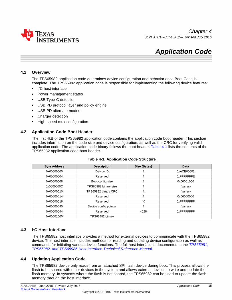
4.2 Application Code Boot HeaderThe first 4kB of the TPS65982 application code contains the application code boot header. This sectionincludes information on the code size and device configuration, as well as the CRC for verifying validapplication code. The application code binary follows the boot header. Table 4-1 lists the contents of theTPS65982 application-code boot header.
Table 4-1. Application Code Structure
Byte Address Description Size (Bytes) Data0x00000000 Device ID 4 0xACE000010x00000004 Reserved 4 0xFFFFFFFE0x00000008 Boot config size 4 0x000010000x0000000C TPS65982 binary size 4 (varies)0x00000010 TPS65982 binary CRC 4 (varies)0x00000014 Reserved 4 0x000000000x00000018 Reserved 40 0xFFFFFFFF0x00000040 Device config pointer 4 (varies)0x00000044 Reserved 4028 0xFFFFFFFF0x00001000 TPS65982 binary
4.3 I2C Host InterfaceThe TPS65982 host interface provides a method for external devices to communicate with the TPS65982device. The host interface includes methods for reading and updating device configuration as well ascommands for initiating various device functions. The full host interface is documented in the TPS65981,TPS65982, and TPS65986 Host Interface Technical Reference Manual.
4.4 Updating Application CodeThe TPS65982 device only reads from an attached SPI flash device during boot. This process allows theflash to be shared with other devices in the system and allows external devices to write and update theflash memory. In systems where the flash is not shared, the TPS65982 can be used to update the flashmemory through the host interface.
Updating Application Code www.ti.com
16 SLVUAH7B–June 2015–Revised July 2016Submit Documentation Feedback
Copyright © 2015–2016, Texas Instruments Incorporated
Application Code
The dual-region memory structure allows for two approaches to application code storage:1. Store firmware in only one half of the memory space. The header with the valid application code has
correct pointers and the header with the invalid application code has pointers set to either 0x000000hor 0xFFFFFFh. When the application code is updated, the new application code is written to theunused half of the memory space. When validated, the region pointers are updated in thecorresponding header and the old header region pointers are set to either 0x000000h or 0xFFFFFFh.Only one region contains the updated code and valid pointers which allows errors to occur duringupdate without overwriting the current code.
2. Store firmware in both halves of the memory space. This method allows redundancy in the memory.Because both halves contain the exact same information, an error may occur in one copy but not in theother. The config page and application code validation checks catch the error and use the other copy.This method also allows protection during application code updating by only updating one copy andthen validating this copy before updating the other copy. If an error occurs during write, whenapplication code is loaded, the invalid application code is ignored.
4.4.1 Application Code Update through I2CThe TPS65982 host interface contains two registers that can be used to execute various routines. TheCmd1 register (0x08) uses information stored in Data1 (0x09) when executing commands, while the Cmd2register (0x10) uses the Data2 register (0x11). For more information on the host interface 4CC commandsand their use, refer to the TPS65981, TPS65982, and TPS65986 Host Interface Technical ReferenceManual.
NOTE: The CmdX register must be read back until it returns a value of 0x00 to determine thecommand is done executing and at least one byte of the DataX register must be read backand used to determine if the command was executed properly (least-significant bit = 0).
When updating the flash memory with the host interface, the following procedure should be followed:Step 1. Determine which region will be updated. The DataX register should by populated with a value
of 0x00 for the low region or 0x01 for the high region.Step 2. Issue the FLrr command to the corresponding CmdX register and once complete read back
the value of the DataX register. The value read back is the address of the chosen region.Step 3. Erase the region header by writing a value of 0x00 for the low region or 0x01 for the high
region to the DataX register and issuing the FLer command.Step 4. Erase the selected region by writing the address from step 2 plus the number of 4kB sectors
to erase to the DataX register and issuing the FLem command in the corresponding CmdXregister.
Step 5. Write the 32-bit address of the application code location from step 2 to the DataX register inthe host interface.
Step 6. Issue the FLad command using the appropriate CmdX register. This instruction sets thelocation stored in step 1 as the start location of the next flash write command.
Step 7. Write up to 64 bytes of the application code to be written to the DataX register.Step 8. Issue the FLwd command to the CmdX register. This command will write the data stored in
the previous step to flash memory starting at the location written in step 1.Step 9. Repeat Step 7 and Step 8 until all of the application code is written. The FLwd command will
auto-increment the write address after each 64-byte chunk. The first 4kB of application codemust be a valid TPS65982 boot header.
Step 10. Write the boot header address of the updated region to the DataX register.Step 11. Execute the FLvy command using the CmdX register. If this command returns 0x00 in the
DataX register the update process was successful.Step 12. If the update verified successfully, update the region pointer with the FLad and FLwd
commands.
www.ti.com Updating Application Code
17SLVUAH7B–June 2015–Revised July 2016Submit Documentation Feedback
Copyright © 2015–2016, Texas Instruments Incorporated
Application Code
4.4.2 Application Code Update through External DeviceThe TPS65982 device only communicates with the flash memory containing the application code duringboot or when a 4CC command has been issued through the host interface. Therefore an external devicecan update the application code while not in use by the TPS65982 device. Any updates made to theapplication code by an external device are required to follow the memory structure described inSection 3.5 and Section 4.2.
OFF
RESET
IDLE ACTIVE SLEEP
VIN_3V3 or VBUS valid
App Code Loaded
ANYSTATE
VIN_3V3VBUSInvalid
HRESET = 1
PT01
PT02
PT03
PT04
18 SLVUAH7B–June 2015–Revised July 2016Submit Documentation Feedback
Copyright © 2015–2016, Texas Instruments Incorporated
Power Management
Chapter 5SLVUAH7B–June 2015–Revised July 2016
Power Management
5.1 Power StatesThe TPS65982 device provides a flexible power and clock management architecture that allows the powerto the analog and digital core to be turned on and off as well as clock dividing or gating to save power indigital circuits. This flexibility allows implementing various power states as shown in Figure 5-1 based onapplication needs.
Figure 5-1. Power State Diagram
The TPS65982 firmware implements the SLEEP, IDLE, and ACTIVE states by programming the hardwareresources. As shown, all entry into low-power states must originate from the ACTIVE state. Similarly, alllow-power states transition to the ACTIVE state upon exiting.
Table 5-1 summarizes the state of the power supplies, oscillators, and functionality that can be supportedin each power state.
(1) Assumes dead-battery support is enabled through RPD_CCn configuration.(2) Assumes dead-battery support is disabled through RPD_CCn configuration.
Table 5-1. Power States Summary
Power Off Dead Battery (1) SLEEP IDLE ACTIVEVIN_3V3 Not Valid Not Valid Valid Valid ValidVBUS Not Valid (1) or Valid (2) Valid Do not care Do not care Do not careLDO_3V3
Disabled Enabled Enabled Enabled EnabledLDO_1V8DLDO_1V8AFOSC_100K OFF ON ON ON ONFOSC_48M OFF ON OFF ON ONUSB Type-C Detection(Cable attach/detach) No Yes Yes Yes Yes
www.ti.com Activity Timer
19SLVUAH7B–June 2015–Revised July 2016Submit Documentation Feedback
Copyright © 2015–2016, Texas Instruments Incorporated
Power Management
Table 5-1. Power States Summary (continued)Power Off Dead Battery (1) SLEEP IDLE ACTIVE
(3) Wake up from SLEEP to ACTIVE upon an I2C message is supported, however, the first I2C message is lost.
I2C No Yes No (3) Yes YesUART No Yes No No YesSPI No Yes No No YesUSB PD No Yes No No Yes
5.2 Activity TimerThe device uses a programmable timer to monitor activity that is occurring while operation is in theACTIVE state. The counter is reset automatically to its programmed value because of the followingevents, and will begin counting again:• Upon entry into the ACTIVE state• I2C activity• UART activity• PD modem activity
If no activity is detected within the programmed time, the activity timer times out, indicating to the firmwarethat the device can exit the active mode and transition to a lower power mode when possible.
The activity timer can be programmed through the host interface using the Sleep Configuration register.Refer to the TPS65981, TPS65982, and TPS65986 Host Interface Technical Reference Manual fordetails.
5.3 System Power StateThe TPS65982 host interface contains a register for storing the system power state. This state does notreflect the power state of the TPS65982 device but rather the state of the surrounding system. TheTPS65982 power-management firmware compares the state stored in the System Power State registerwith the state stored in the second byte of the Sleep Configuration register when attempting to enter asleep state. If the system power state is equal to or less than the state of the Sleep Configuration register,the TPS65982 device enters the lowest power sleep state. If the stored value is greater than that of theSleep Configuration register, the TPS65982 device enters the higher power idle state.
NOTE: Higher hex values correspond to lower power states. Such that 0x00 is the highest powerstate (S0) and 0xFE is the lowest power state (S254).
5.4 Power State Descriptions
5.4.1 POWER OFFThe TPS65982 device is in the POWER OFF state when VIN_3V3 and VBUS are not valid.
5.4.2 RESETThe TPS65982 device has a POR (power-on-reset) circuit that initializes the device when VIN_3V3 orVBUS are valid. While in the RESET state the TPS65982 device carries out boot code and RESETZ isasserted until VOUT_3V3 is valid and TUVRDELAY has elapsed. After application code has loaded, theTPS65982 device transitions into the ACTIVE state.
5.4.3 SLEEPSleep is the low-power state of TPS65982 device. Sleep state can only be entered while the device isunattached or operating in a legacy 5-V application. During SLEEP state the device operates from the100-kHz oscillator to monitor for wake-up events and communication with the device is disabled.
Power State Descriptions www.ti.com
20 SLVUAH7B–June 2015–Revised July 2016Submit Documentation Feedback
Copyright © 2015–2016, Texas Instruments Incorporated
Power Management
5.4.3.1 Entry to the SLEEP (Power Transition 01 – PT01)Entry to the SLEEP state is only possible from the ACTIVE state. Entry to the SLEEP occurs because ofthe following events:• The system power state is equal to or less than state set in the Sleep Configuration Register
(controlled by the host interface).• No cable attached or cable detach event occurs.• The device is a source connected to a non-PD capable sink or device is configured as a non-PD
capable sink (controlled by the host interface).• The activity timer times out (controlled by the host interface).
5.4.3.2 Exit from SLEEP (Power Transition 02 – PT02)Exit from the SLEEP state is always to ACTIVE. Exit from SLEEP occurs because of the following events:• Any reset event• I2C bus activity• Any enabled interrupt event (I2C interrupt request, supervisor events, CC attach or detach events, and
so forth)
NOTE: For DRP and sink with accessory ports that require DRP toggle and accessory toggleoperations, respectively, the TPS65982 device supports the toggle operations completelywhile operating in SLEEP. Therefore, no transition to ACTIVE is required to perform thetoggle operation which enables significant power consumption savings for DRP and sink withaccessory ports while in the Unattached.SNK and Unattached.SRC states.
Upon exiting SLEEP, the TPS65982 device transitions to ACTIVE. The TPS65982 device enablesFOSC_48M and waits for it to stabilize before releasing it to the digital core.
5.4.4 IDLEThe IDLE state is a low-power state similar to SLEEP, except that the high-speed oscillator is kept activeto allow the TPS65982 device to continue to respond immediately to I2C commands. While in IDLE,processing is enabled, however, with a clock frequency of 6 MHz. The TPS65982 device advertises itselfon CC1 and CC2 according to the configuration and monitors USB Type-C Port for attach or detach.
5.4.4.1 Entry to the IDLE (Power Transition 03 – PT03)Entry to the IDLE state is only possible from the ACTIVE state. Entry to the IDLE occurs because of thefollowing events:• The system power state is greater than state set in Sleep Configuration Register (controlled by the
host interface).• No cable attached or cable detach event occurs.• The device is a source connected to a non-PD capable sink or device is configured as a non-PD
capable sink (controlled by the host interface).• The activity timer times out (controlled by the host interface).
5.4.4.2 Exit from IDLE (Power Transition 04 – PT04)Exit from the IDLE state is always to ACTIVE. Exit from IDLE occurs because of the following events:• Any enabled interrupt event (I2C interrupt request, supervisor events, CC detach events, and so forth)
except host command events.• Any reset event
www.ti.com Power State Descriptions
21SLVUAH7B–June 2015–Revised July 2016Submit Documentation Feedback
Copyright © 2015–2016, Texas Instruments Incorporated
Power Management
5.4.5 ACTIVEThe ACTIVE state is an operational state where either USB PD or USB2.0 data transmission activityhappens on the USB Type-C Port and the TPS65982 device responds to configuration and statuscommands from the host through the I2C interface. The TPS65982 device is usually in one of attached(DFP, UFP, or Alternate Mode) USB Type-C Port states in the ACTIVE state. The TPS65982 deviceadvertises itself on CC1 and CC2 as according to the configuration and monitors USB Type-C Port forattach or detach. The TPS65982 device runs the policy engine and all associated hardware and softwarelogic if USB PD communication is required.
5.4.5.1 Entry to the ACTIVEEntry to the ACTIVE state occurs because of the following events:• Exit from all low-power states transition to ACTIVE• Reset event
5.4.5.2 Exit from ACTIVEExit from the ACTIVE state to any low-power states meeting the criteria for entry into the respective low-power state.
5.4.6 Dead BatteryIn systems where the battery is unable to provide adequate power to the TPS65982 VIN_3V3 supply, theTPS65982 dead-battery mode allows the device to power from VBUS. VBUS power can also be passed tothe system to allow for battery charging. While in the DEAD BATTERY state, the TPS65982 deviceoperates as if the Type-C connection is the only source of power to the system.
5.4.6.1 Entry to the Dead BatteryThe TPS65982 dead-battery behavior is defined by the configuration of RPD_G1 and RPD_G2 pins.These pins can be connected to C_CC1 and C_CC2, respectively, to enable dead-battery support.Alternately, they may be connected to ground to disable dead-battery support.
If dead-battery support is enabled, when connected to a source, an unpowered TPS65982 powers the Rdresistors from the C_CC1 and C_CC2 pins and advertises itself as a Sink.
In response, the source provides VBUS power and the TPS65982 device initiates the boot flow. Duringboot, the TPS65982 device samples the BUSPOWERZ pin to determine if VBUS is received by thesystem through the PP_EXT path, or the PP_HV path. The device then continues through the RESETstate, carrying out the boot flow and loading the application code.
Dead-battery operation is indicated by the dead-battery flag located in register 0x2D of the host interface.The flag is set by the TPS65982 bootloader upon detection of dead-battery conditions.
5.4.6.2 Dead Battery RestrictionsWhile in dead-battery mode certain functions of the TPS65982 device are restricted to ensure power fromVBUS is not lost. The TPS65982 port type is restricted to sink only, and all power role-swap requests arerejected. Additionally only the dead-battery power switch (configured through BUSPOWERZ) is allowed toclose. Because of this behavior, TI recommends that the sink switch defined in the device systemconfiguration match the switch enabled by BUSPOWERZ.
The TPS65982 device does not source VCONN while operating in dead-battery mode, and rejects anyVCONN swap requests.
5.4.6.3 Exit from Dead BatteryDead-battery operation can be exited in one of the following ways:• Executing the DBfg host interface 4CC command• High edge occurring on a GPIO configured with BARREL_JACK_EVENT
Power State Descriptions www.ti.com
22 SLVUAH7B–June 2015–Revised July 2016Submit Documentation Feedback
Copyright © 2015–2016, Texas Instruments Incorporated
Power Management
• VBUS removal during dead-battery operation• Thermal protection event occurring
The DBfg 4CC command upon execution clears the dead-battery flag used to indicate dead-batteryoperation and exits the dead-battery mode. The DBfg command is primary method for exiting dead-batterymode, and should be issued by an attached embedded controller once the system is self-sustainable andable to provide VIN_3V3.
The GPIO event labeled, BARREL_JACK_EVENT, issues the DBfg command upon detection of a risingedge. This event can be used to clear the dead-battery flag upon application of an external power source.The external power source should be tied to the GPIO through a resistor divider such that the GPIO is atthe programed I/O voltage when the external source is present. For more information on the barrel jackGPIO event see Table 13-1.
If VBUS is removed during dead-battery operation, the TPS65982 device issues a cold device reset. Thisreset causes the device to restart the boot process, forcing a reevaluation of the VIN_3V3 state.
23SLVUAH7B–June 2015–Revised July 2016Submit Documentation Feedback
Copyright © 2015–2016, Texas Instruments Incorporated
USB Type-C
Chapter 6SLVUAH7B–June 2015–Revised July 2016
USB Type-C
6.1 OverviewMain functionality supported:• USB Type-C port configuration• CC detection• USB Type-C connection state machines for:
– Downstream facing port (DFP)– Upstream facing port (UFP)– UFP with accessory support– Dual-role port (DRP)– DRP with accessory and Try.SRC support
• Accessory modes– Audio Adapter Accessory Mode– Debug Accessory Mode
6.2 USB Type-C Port ConfigurationThe TPS65982 firmware supports configuring the USB Type-C port based on the needs and capabilities ofthe system. These USB Type-C port configurations include:• Power capabilities of the port (sink, source, DRP)• Receptacle type• USB Type-C current advertisement for a port that has power sourcing capabilities (source, DRP)• VCONN support modes• VBUS power switch settings• VCONN power switch settings
The device configuration is initially loaded from the configuration data loaded along with the applicationcode. Additionally the TPS65982 host interface allows access to a System Configuration register wherethese USB Type-C port configurations can be written to or read from. For more information about all theUSB Type-C port configurations offered, see the System Configurations register bit field definitions in theTPS65981, TPS65982, and TPS65986 Host Interface Technical Reference Manual.
6.2.1 SourceWhen configured as a source by the application code Config Data, the TPS65982 device disables theVBUS power path and VCONN power path and enables the CC pin pullup current sources. The devicethen enters the USB Type-C state machine in the Unattached.SRC state and waits for a connection on theUSB Type-C port.
6.2.2 SinkWhen configured as a sink by the application-code configuration data, the TPS65982 device enables thepulldown resistors on the CC pins and the VBUS detection circuitry. The device then enters the USBType-C state machine in the Unattached.SNK state, and waits for a connection on the USB Type-C port.
CC Detection www.ti.com
24 SLVUAH7B–June 2015–Revised July 2016Submit Documentation Feedback
Copyright © 2015–2016, Texas Instruments Incorporated
USB Type-C
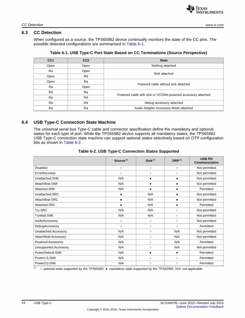
6.3 CC DetectionWhen configured as a source, the TPS65982 device continually monitors the state of the CC pins. Thepossible detected configurations are summarized in Table 6-1.
Table 6-1. USB Type-C Port State Based on CC Terminations (Source Perspective)
CC1 CC2 StateOpen Open Nothing attached
Rd OpenSink attached
Open RdOpen Ra
Powered cable without sink attachedRa OpenRd Ra
Powered cable with sink or VCONN-powered accessory attachedRa RdRd Rd Debug accessory attachedRa Ra Audio Adapter Accessory Mode attached
6.4 USB Type-C Connection State MachineThe universal serial bus Type-C cable and connector specification define the mandatory and optionalstates for each type of port. While the TPS65982 device supports all mandatory states, the TPS65982USB Type-C connection state machine can support optional states selectively based on OTP configurationbits as shown in Table 6-2.
(1) ○: optional state supported by the TPS65982, ●: mandatory state supported by the TPS65982, N/A: not applicable
Table 6-2. USB Type-C Connection States Supported
Source (1) Sink (1) DRP (1) USB PDCommunication
Disabled ○ ○ ○ Not permittedErrorRecovery ○ ○ ○ Not permittedUnattached.SNK N/A ● ● Not permittedAttachWait.SNK N/A ● ● Not permittedAttached.SNK N/A ● ● PermittedUnattached.SRC ● N/A ● Not permittedAttachWait.SRC ● N/A ● Not permittedAttached.SRC ● N/A ● PermittedTry.SRC N/A N/A ○ Not permittedTryWait.SNK N/A N/A ○ Not permittedAudioAccessory ○ ○ ○ Not permittedDebugAccessory ○ ○ ○ PermittedUnattached.Accessory N/A ○ N/A Not permittedAttachWait.Accessory N/A ○ N/A Not permittedPowered.Accessory N/A ○ N/A PermittedUnsupported.Accessory N/A ○ N/A Not permittedPowerDefault.SNK N/A ● ● PermittedPower1.5.SNK N/A ○ ○ PermittedPower3.0.SNK N/A ○ ○ Permitted
25SLVUAH7B–June 2015–Revised July 2016Submit Documentation Feedback
Copyright © 2015–2016, Texas Instruments Incorporated
Accessory Modes
Chapter 7SLVUAH7B–June 2015–Revised July 2016
Accessory Modes
7.1 Audio Accessory ModeThe TPS65982 enters Audio Adapter Accessory Mode when it detects the states of both CC pins atSRC.Ra (that is, the analog audio adapter identifies itself by presenting a resistance to ground of ≤ Ra onboth CC and VCONN pin of the USB Type-C plug).
When in Audio Adaptor Accessory Mode, the USB Type-C port mux is unused. Because the audio signalsare routed externally to the Type-C connector, the USB Type-C port mux must be set to high impedance(Hi-Z).
7.2 Debug Accessory ModeThe TPS65982 device enters Debug Accessory Mode when it detects the states of both CC pins atSRC.Rd range (that is, the debug accessory identifies itself by presenting a resistance to Rd on both CCand VCONN pin of the USB Type-C plug).The TPS65982 device configures the USB Type-C portmultiplexor. The TPS65982 device requires no checks for proper orientation of the debug accessory. Theuser is assumed to be responsible for providing the proper orientation of the debug accessory.
The system port signals, UART_TX and UART_RX, are rerouted by the digital crossbar inside the digitalcore. The UART_TX and UART_RX signals are level shifted and buffered, routed through the cross barmux, and level shifted to the USB Type-C port signals C_USB_BP and C_USB_BN, respectively. Inaddition, the system port signals USB_RP and USB_RN are routed as analog signals to the USB Type-Cport signals C_USB_TP and C_USB_TN, respectively. Lastly, the system port signals SWD_CLK andSWD_DIO are routed as analog signals to the USB Type-C port signals SBU1 and SBU2, respectively.
26 SLVUAH7B–June 2015–Revised July 2016Submit Documentation Feedback
Copyright © 2015–2016, Texas Instruments Incorporated
Type-C Port Multiplexer Configurations
Chapter 8SLVUAH7B–June 2015–Revised July 2016
Type-C Port Multiplexer Configurations
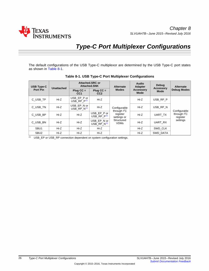
The default configurations of the USB Type-C multiplexor are determined by the USB Type-C port statesas shown in Table 8-1.
(1) USB_EP or USB_RP connection dependent on system configuration settings.
Table 8-1. USB Type-C Port Multiplexer Configurations
USB Type-CPort Pin Unattached
Attached.SRC orAttached.SNK Alternate
Modes
AudioAdapter
AccessoryMode
DebugAccessory
ModeAlternate
Debug ModesPlug CC =CC1
Plug CC =CC2
C_USB_TP Hi-Z USB_EP_P orUSB_RP_P (1) Hi-Z
Configurablethrough I2C
registersettings orStructured
VDMs
Hi-Z USB_RP_P
Configurablethrough I2C
registersettings
C_USB_TN Hi-Z USB_EP_N orUSB_RP_N (1) Hi-Z Hi-Z USB_RP_N
C_USB_BP Hi-Z Hi-Z USB_EP_P orUSB_RP_P (1) Hi-Z UART_TX
C_USB_BN Hi-Z Hi-Z USB_EP_N orUSB_RP_N (1) Hi-Z UART_RX
SBU1 Hi-Z Hi-Z Hi-Z Hi-Z SWD_CLKSBU2 Hi-Z Hi-Z Hi-Z Hi-Z SWD_DATA
27SLVUAH7B–June 2015–Revised July 2016Submit Documentation Feedback
Copyright © 2015–2016, Texas Instruments Incorporated
USB Power Delivery
Chapter 9SLVUAH7B–June 2015–Revised July 2016
USB Power Delivery
9.1 OverviewThe TPS65982 USB Power Delivery firmware allows pairs of directly attached ports to negotiate voltage,current, direction of power flow over the USB cable or all of these, using the CC wire as thecommunications channel.
The Physical Layer firmware handles transmission and reception of bits on the CC wire.
The Protocol Layer firmware enables messages to be exchanged between a Source Port and a Sink Port.
The Policy Engine firmware implements the Local Policy for the Port.
The TPS65982 USB Power Delivery firmware supports Standard and Vendor defined Modal Operation.
9.2 Protocol LayerThe TPS65982 Protocol Layer firmware forms the messages used to communicate information between apair of ports. The firmware is responsible for forming capabilities messages, requests andacknowledgments. Additionally, the firmware forms messages used to swap roles and maintain presence.The firmware receives inputs from the policy engine indicating which messages to send and indicates theresponses back to the policy engine.
The basic protocol uses a push model where the source pushes the capabilities to the sink that, in turn,responds with a request based on the offering. However, the sink can asynchronously request the presentcapabilities of the source and can select another voltage or current.
The TPS65982 protocol layer implements the following according to the Universal Serial Bus PowerDelivery Specification:• Control messages• Data messages• Timers• Counters• Reset
9.2.1 Control MessagesTable 9-1 summarizes control messages supported by the TPS65982 protocol layer.
Table 9-1. Control Messages
Control Message Sent byGoodCRC Source, sink or cable plugGoToMin Source onlyAccept Source, sink or cable plugReject Source or sinkPing Source onlyPS_RDY Source or sinkGet_Source_Cap Source or sinkGet_Sink_Cap Source or sinkDR_Swap Source or sink
Protocol Layer www.ti.com
28 SLVUAH7B–June 2015–Revised July 2016Submit Documentation Feedback
Copyright © 2015–2016, Texas Instruments Incorporated
USB Power Delivery
Table 9-1. Control Messages (continued)Control Message Sent byPR_Swap Source or sinkVCONN_Swap DFPWait Source or sinkSoft Reset Source or sink
9.2.2 Data MessagesThe TPS65982 firmware supports the following data message types:• Source capabilities• Request• BIST• Sink capabilities• Vendor defined
9.2.2.1 Power Data ObjectsPower data objects (PDOs) are used by USB Power Delivery messages to communicate the powercapabilities or power requirements of a source. The TPS65982 host interface and system configurationallows for seven PDOs to be implemented and stored on the device. When defining device PDOs, careshould be taken to avoid overlap of the voltage capabilities of the PDO as the TPS65982 device does notsupport these configurations.
9.2.3 ResetThe TPS65982 firmware implements both soft reset and hard reset as defined by the USB Power DeliverySpecification.
A soft reset message is used to cause a soft reset of the protocol communication when it has brokendown in some way. The soft reset does not have any impact on power supply operation and may betriggered by either port partner in response to an error.
A hard reset is signaled by an ordered set. Both the sender and recipient reset both the power suppliesand protocol.
9.3 Policy EngineThe Universal Serial Bus Power Delivery Specification defines and provides detailed message sequencesand associated timing requirements. Because the message sequences are explicitly described in theUniversal Serial Bus Power Delivery Specification, this document establishes a framework for supportedmessage sequences and refers to the Universal Serial Bus Power Delivery Specification referenced inSection 1.2. The USB standards documents should be referenced for the latest information.
Table 9-2. USB PD Message Sequences Supported by the TPS65982
Message sequence Message sub-sequencePower NegotiationReclaiming Power with GoToMin messageSoft ResetHard Reset Source Initiated Hard Reset
Sink Initiated Hard ResetSource Initiated Hard Reset – Sink Long Reset
Type-C Power Role Swap Type-C Source Initiated Power Role Swap without subsequentPower Negotiations
www.ti.com Policy Engine
29SLVUAH7B–June 2015–Revised July 2016Submit Documentation Feedback
Copyright © 2015–2016, Texas Instruments Incorporated
USB Power Delivery
Table 9-2. USB PD Message Sequences Supported by the TPS65982 (continued)Message sequence Message sub-sequence
Type-C Sink Initiated Power Role Swap without subsequentPower Negotiation
Type-C Data Role Swap Type-C Data Role Swap, Initiated by UFP Operating as SinkType-C Data Role Swap, Initiated by UFP Operating as SourceType-C Data Role Swap, Initiated by DFP Operating as SourceType-C Data Role Swap, Initiated by DFP Operating as Sink
Type-C VCONN Type-C DFP to UFP VCONN Source SwapType-C UFP to DFP VCONN Source Swap
Structured VDM DFP to UFP Discover IdentitySource Port to Cable Plug Discover IdentityDFP to Cable Plug Discover IdentityDFP to UFP Enter ModeDFP to UFP Exit ModeDFP to Cable Plug Enter ModeDFP to Cable Plug Exit ModeUFP to DFP AttentionCable Plug to DFP Attention
Built in Self-Test (BIST) BIST Receiver ModeBIST Transmit ModeBIST Test Patterns
9.3.1 Request MessageDuring power negotiation, the sink port sends a Request message to request power in response to themost recent Source Capabilities message. The Request message returns one sink request data object(RDO) that identifies the power data object (PDO) being requested. The USB Power Delivery specificationdescribes the various types of Request messages depending on the type of supply (fixed, battery, orvariable).
When the TPS65982 device is operating as a sink, the policy engine firmware selects the source PDO ofmatching supply type that will deliver maximum power. When the sink cannot satisfy its powerrequirements from the capabilities offered by the source, the sink sets the Capability Mismatch bit in RDO.
9.3.1.1 Automatic Request NegotiationWhen operating as a sink, the TPS65982 device can automatically select the best source capability andsend the appropriate request message. The TPS65982 device determines the sink capability from thepower data objects stored in the 0x33 TX Sink Capabilities Register. The settings stored in the0x37 AutoNegotiate Sink Register are then used to prioritize and select the best received source PDO. The selectedPDO is determined using the following process:
Step 1. Attempt to determine the best PDO using the user defined priority set in the Offer Priority fieldof the Auto Negotiate Sink Register.
Step 2. If multiple PDOs exist of equal priority, select based on supply type: fixed supply, thenvariable supply, then battery supply.
Step 3. Select PDO based on highest offered peak current.
30 SLVUAH7B–June 2015–Revised July 2016Submit Documentation Feedback
Copyright © 2015–2016, Texas Instruments Incorporated
Alternate Modes
Chapter 10SLVUAH7B–June 2015–Revised July 2016
Alternate Modes
10.1 OverviewThe Universal Serial Bus Type-C Cable and Connector Specification provides support for alternate modesusing the USB Type-C connector and cables. In an alternate mode various pins on the USB Type-Cconnector may be reconfigured to support interfaces outside the scope of USB Type-C.
The TPS65982 device implements the discovery process as outlined in the Universal Serial Bus Type-CCable and Connector Specification (and Universal Serial Bus Power Delivery Specification, which itleverages) for discovering the support of alternate modes in connected devices, including the method forswitching into and out of a mode.
10.2 USB BillboardThe integrated USB low-speed endpoint of the TPS65982 device allows the device to comply with USBType-C standards without needing additional external billboard devices. After a UFP attach event, if analternate mode is not entered after one second has elapsed, the TPS65982 device exposes the USBbillboard. The USB billboard can be provided by the integrated USB endpoint of the TPS65982 device orby an externally provided endpoint on the devices USB_RP pins. The TPS65982 firmware only supportsthe EP0 control endpoint.
10.3 Automatic EntryWhen attached to a port partner supporting alternate mode, the TPS65982 device automatically attemptsto negotiate mode entry for discovered alternate modes.
For modes that require the use of connector resources, such as the SBU lines, or are mutually exclusive,the Alternate Mode Automatic Entry Sequence Register of the host interface should be used. Whennegotiating alternate modes the TPS65982 device prioritizes mode entry based on mode order in thisregister. When a mode in the register is entered, mode entry for other modes listed will not be attempted.
10.4 DisplayPort Alternate ModeThe TPS65982 device supports DisplayPort as found in the DisplayPort Alt Mode Standard and containshardware to support HPD handling. Figure 10-1 shows the TPS65982 process for handling HPD as a DPsink (UFP_D).
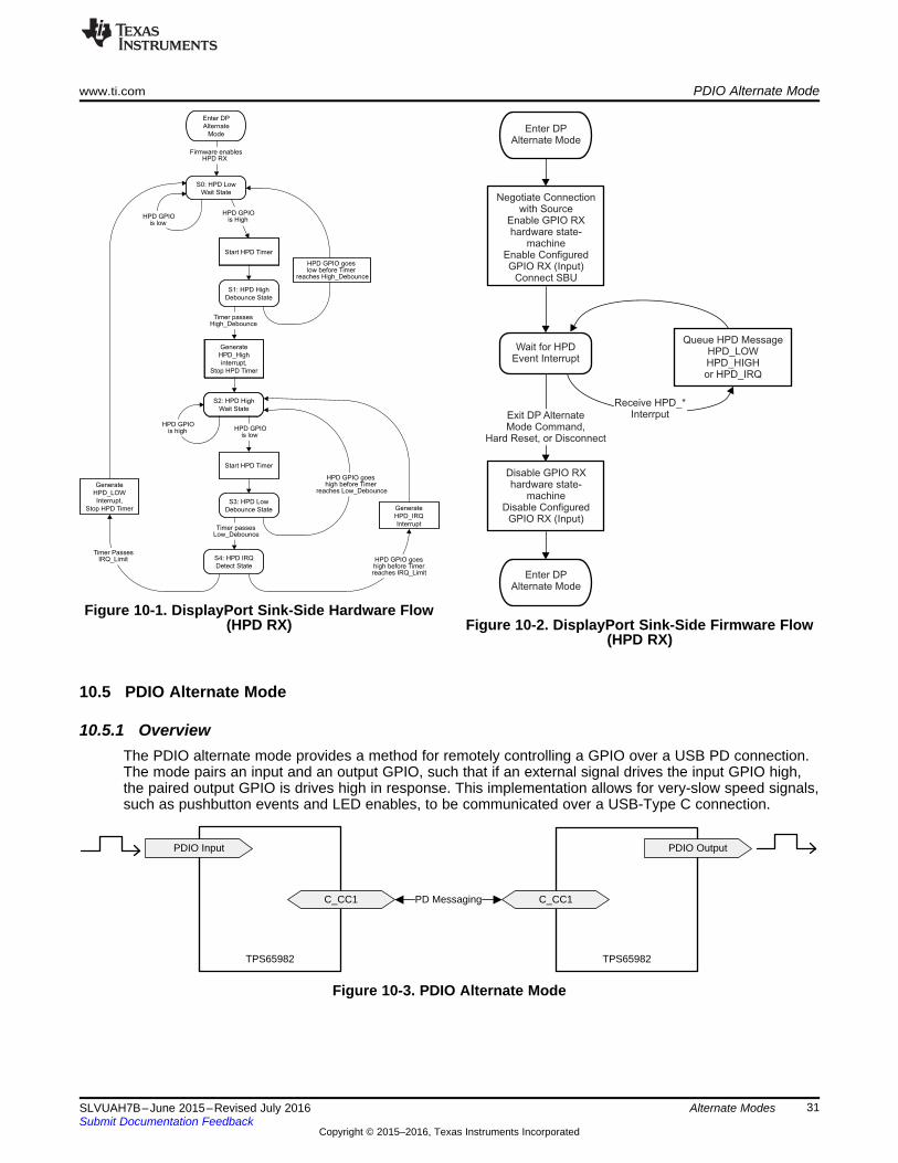
TPS65982 TPS65982
PD MessagingC_CC1 C_CC1
PDIO Input PDIO Output
Negotiate Connectionwith Source
Enable GPIO RXhardware state-
machineEnable ConfiguredGPIO RX (Input)
Connect SBU
Wait for HPDEvent Interrupt
Queue HPD MessageHPD_LOWHPD_HIGHor HPD_IRQ
Receive HPD_*Interrput
Disable GPIO RXhardware state-
machineDisable Configured
GPIO RX (Input)
Exit DP AlternateMode Command,
Hard Reset, or Disconnect
Enter DPAlternate Mode
Enter DPAlternate Mode
Enter DP
Alternate
Mode
S0: HPD Low
Wait State
Firmware enablesHPD RX
Start HPD Timer
HPD GPIOis High
S1: HPD High
Debounce State
HPD GPIOis low
HPD GPIO goeslow before Timer
reaches High_Debounce
Generate
HPD_High
interrupt,
Stop HPD Timer
Timer passesHigh_Debounce
S2: HPD High
Wait State
HPD GPIOis high
Start HPD Timer
HPD GPIOis low
S3: HPD Low
Debounce State
HPD GPIO goeshigh before Timer
reaches Low_Debounce
S4: HPD IRQ
Detect State
Timer passesLow_Debounce
Generate
HPD_IRQ
Interrupt
HPD GPIO goeshigh before Timerreaches IRQ_Limit
Generate
HPD_LOW
Interrupt,
Stop HPD Timer
Timer PassesIRQ_Limit
www.ti.com PDIO Alternate Mode
31SLVUAH7B–June 2015–Revised July 2016Submit Documentation Feedback
Copyright © 2015–2016, Texas Instruments Incorporated
Alternate Modes
Figure 10-1. DisplayPort Sink-Side Hardware Flow(HPD RX) Figure 10-2. DisplayPort Sink-Side Firmware Flow
(HPD RX)
10.5 PDIO Alternate Mode
10.5.1 OverviewThe PDIO alternate mode provides a method for remotely controlling a GPIO over a USB PD connection.The mode pairs an input and an output GPIO, such that if an external signal drives the input GPIO high,the paired output GPIO is drives high in response. This implementation allows for very-slow speed signals,such as pushbutton events and LED enables, to be communicated over a USB-Type C connection.
Figure 10-3. PDIO Alternate Mode
PDIO Alternate Mode www.ti.com
32 SLVUAH7B–June 2015–Revised July 2016Submit Documentation Feedback
Copyright © 2015–2016, Texas Instruments Incorporated
Alternate Modes
10.5.2 PDIO GPIO EventsThe PDIO alternate mode uses four pairs of GPIO events to configure the TPS65982 GPIOs as either aPDIO input or PDIO output. The events are pair such that the state of the PDIO_OUT0 GPIO mirrors anychanges made to the PDIO_IN0 GPIO. Each TPS65982 device can have four GPIOs configured as PDIOinputs and four GPIOs configured as PDIO outputs. For more information on GPIO events see Table 13-1.
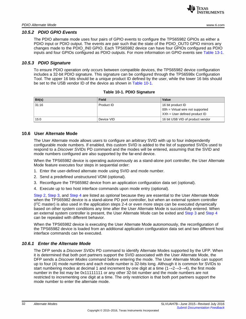
10.5.3 PDIO SignatureTo ensure PDIO operation only occurs between compatible devices, the TPS65982 device configurationincludes a 32-bit PDIO signature. This signature can be configured through the TPS6598x ConfigurationTool. The upper 16 bits should be a unique product ID defined by the user, while the lower 16 bits shouldbe set to the USB vendor ID of the device as shown in Table 10-1.
Table 10-1. PDIO Signature
Bit(s) Field Value31:16 Product ID 16 bit product ID
00h = Virtual wire not supportedXXh = User defined product ID
15:0 Device VID 16 bit USB VID of product vendor
10.6 User Alternate ModeThe User Alternate mode allows users to configure an arbitrary SVID with up to four independentlyconfigurable mode numbers. If enabled, this custom SVID is added to the list of supported SVIDs used torespond to a Discover SVIDs PD command and the modes will be entered, assuming that the SVID andmode numbers configured are also supported by the far-end device.
When the TPS65982 device is operating autonomously as a stand-alone port controller, the User AlternateMode feature executes four steps in sequential order:1. Enter the user-defined alternate mode using SVID and mode number.2. Send a predefined unstructured VDM (optional).3. Reconfigure the TPS65982 device from an application configuration data set (optional).4. Execute up to two host interface commands upon mode entry (optional).
Step 2, Step 3, and Step 4 are listed as optional because they are essential to the User Alternate Modewhen the TPS65982 device is a stand-alone PD port controller, but when an external system controller(I2C master) is also used in the application steps 2-4 or even more steps can be executed dynamicallybased on other system conditions any time after the User Alternate Mode is successfully entered. Whenan external system controller is present, the User Alternate Mode can be exited and Step 3 and Step 4can be repeated with different behavior.
When the TPS65982 device is executing the User Alternate Mode autonomously, the reconfiguration ofthe TPS65982 device is loaded from an additional application configuration data set and two different hostinterface commands can be executed.
10.6.1 Enter the Alternate ModeThe DFP sends a Discover SVIDs PD command to identify Alternate Modes supported by the UFP. Whenit is determined that both port partners support the SVID associated with the User Alternate Mode, theDFP sends a Discover Modes command before entering the mode. The User Alternate Mode can supportup to four (4) mode numbers and each mode number is 32-bits long. Although it is common for SVIDs tostart numbering modes at decimal 1 and increment by one digit at a time (1→2→3→4), the first modenumber in the list may be 0x11111111 or any other 32-bit number and the mode numbers are notrestricted to incrementing one digit at a time. The only restriction is that both port partners support themode number to enter the alternate mode.
www.ti.com User Alternate Mode
33SLVUAH7B–June 2015–Revised July 2016Submit Documentation Feedback
Copyright © 2015–2016, Texas Instruments Incorporated
Alternate Modes
10.6.2 Send Unstructured Vendor-Defined MessageThe ability to send a pre-defined unstructured vendor-defined message (VDM) upon mode entry isgenerally used to advertise an identity. One practical example of a custom alternate mode iscommunicating between battery-powered products and compatible power supplies. A power supply thatdoes not contain a dedicated processor can use the integrated processor of the TPS65982 toautomatically send an unstructured VDM advertising the power supply's model number, revision, serialnumber, and others.
10.6.3 Reconfigure the TPS65982 from Data SetThe ability to reconfigure the TPS65982 device allows modification of any of the configuration registers ofthe host interface automatically upon mode entry from a data set stored in flash memory. This can beused, for instance, to modify the power sourcing and sinking capabilities of the PD port when compatibleproducts are attached. Any register listed as read/write (R/W) in the TPS65981, TPS65982, andTPS65986 Host Interface Technical Reference Manual and accessible in the TPS6598X ApplicationCustomization Tool can be reconfigured upon mode entry and the registers that need to be modified willvary based on the application.
10.6.4 Execute Host-Interface CommandsAfter reconfiguration of the host interface registers, up to two host-interface 4CC commands may beexecuted. The first 4CC command that is executed is an internal command that modifis the behavior of theTPS65982 device. A practical example is driving a GPIO high or low to indicate alternate mode entry orclearing the dead-battery flag to indicate external power is available. The second 4CC command that isexecuted can be an internal command or a PD task. A practical example of a PD task is forcingrenegotiation of the PD power contract or issuing a data-role or power-role swap request.
34 SLVUAH7B–June 2015–Revised July 2016Submit Documentation Feedback
Copyright © 2015–2016, Texas Instruments Incorporated
Power Delivery Fault Handling
Chapter 11SLVUAH7B–June 2015–Revised July 2016
Power Delivery Fault Handling
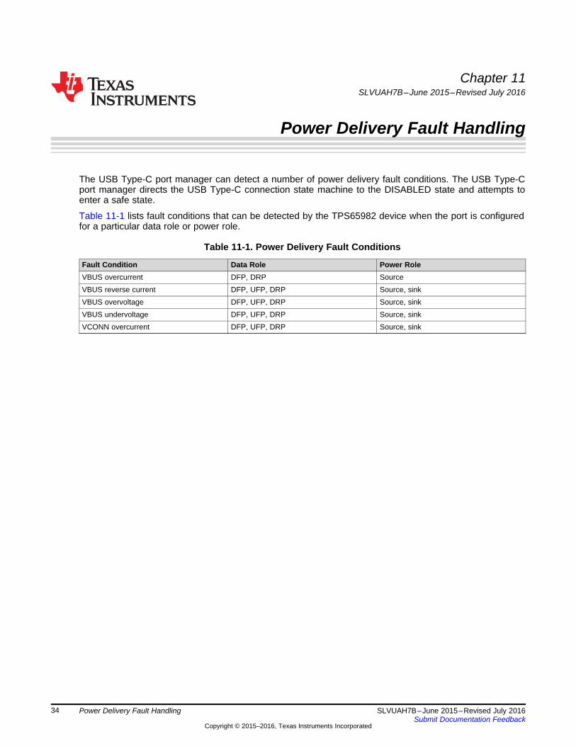
The USB Type-C port manager can detect a number of power delivery fault conditions. The USB Type-Cport manager directs the USB Type-C connection state machine to the DISABLED state and attempts toenter a safe state.
Table 11-1 lists fault conditions that can be detected by the TPS65982 device when the port is configuredfor a particular data role or power role.
Table 11-1. Power Delivery Fault Conditions
Fault Condition Data Role Power RoleVBUS overcurrent DFP, DRP SourceVBUS reverse current DFP, UFP, DRP Source, sinkVBUS overvoltage DFP, UFP, DRP Source, sinkVBUS undervoltage DFP, UFP, DRP Source, sinkVCONN overcurrent DFP, UFP, DRP Source, sink
DCD Detector
DCD Timeout
Enter ChargerDetection
DCD
Primary Detection
SecondaryDetection
Exit ChargerDetection
No Detection
SDPNot Detected
Set Charger = DCP
Set Charger = CDP
Set Charger = SDP
SDPDetected
Set Charger = None
DCPDetected
CDPDetected
35SLVUAH7B–June 2015–Revised July 2016Submit Documentation Feedback
Copyright © 2015–2016, Texas Instruments Incorporated
Charger Detection
Chapter 12SLVUAH7B–June 2015–Revised July 2016
Charger Detection
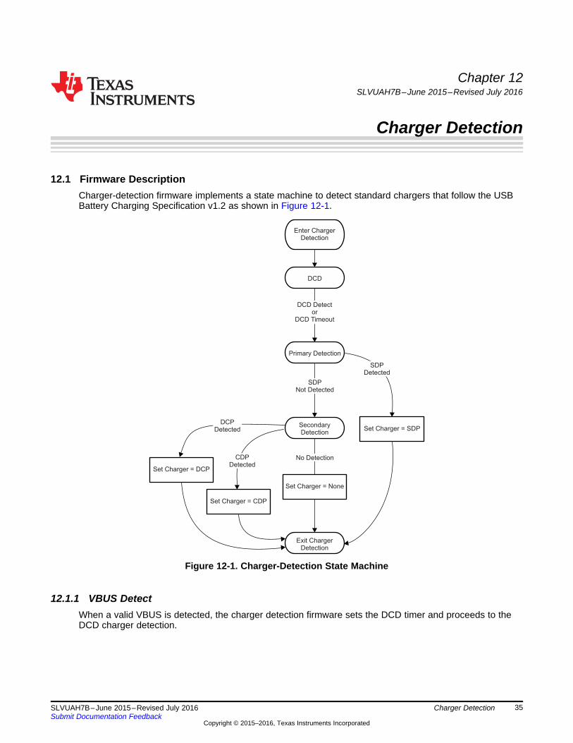
12.1 Firmware DescriptionCharger-detection firmware implements a state machine to detect standard chargers that follow the USBBattery Charging Specification v1.2 as shown in Figure 12-1.
Figure 12-1. Charger-Detection State Machine
12.1.1 VBUS DetectWhen a valid VBUS is detected, the charger detection firmware sets the DCD timer and proceeds to theDCD charger detection.
D+ < VLGC?
DCD debounce timer expired?
Yes
No
Yes
No
Enable IDP_SRC on D+, RDM_DWN on
D±
Set DCD debounce timer to
TDCD_DBNC
Disable IDP_SRC, RDM_DWN
Primary Detection
Set DCD toggle timer to TDCD_TOGGLE
DCD timer expired?
No
Disable IDP_SRC, RDM_DWN
Data Contact Detected
Yes
Firmware Description www.ti.com
36 SLVUAH7B–June 2015–Revised July 2016Submit Documentation Feedback
Copyright © 2015–2016, Texas Instruments Incorporated
Charger Detection
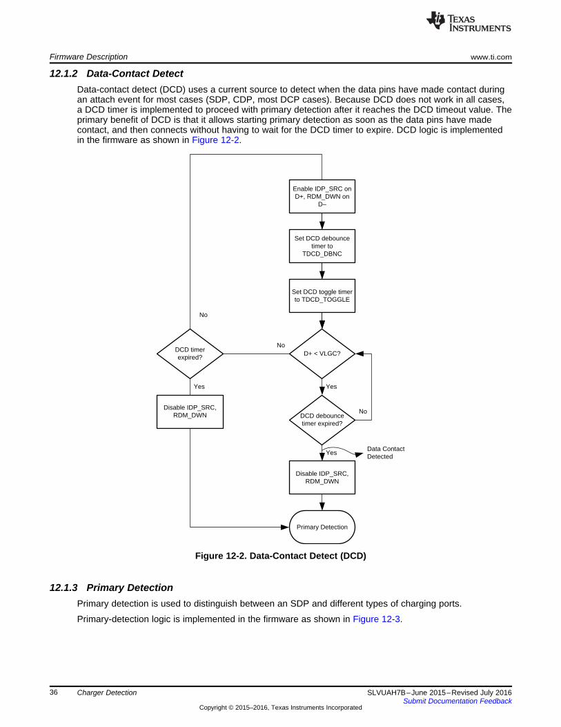
12.1.2 Data-Contact DetectData-contact detect (DCD) uses a current source to detect when the data pins have made contact duringan attach event for most cases (SDP, CDP, most DCP cases). Because DCD does not work in all cases,a DCD timer is implemented to proceed with primary detection after it reaches the DCD timeout value. Theprimary benefit of DCD is that it allows starting primary detection as soon as the data pins have madecontact, and then connects without having to wait for the DCD timer to expire. DCD logic is implementedin the firmware as shown in Figure 12-2.
Figure 12-2. Data-Contact Detect (DCD)
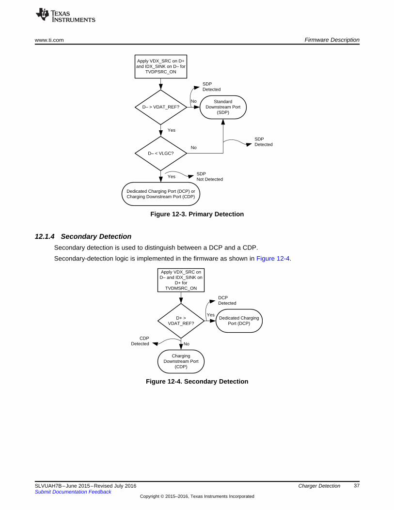
12.1.3 Primary DetectionPrimary detection is used to distinguish between an SDP and different types of charging ports.
Primary-detection logic is implemented in the firmware as shown in Figure 12-3.
Apply VDX_SRC on D± and IDX_SINK on
D+ for TVDMSRC_ON
D+ > VDAT_REF?
Dedicated Charging Port (DCP)
Charging Downstream Port
(CDP)
Yes
NoCDP
Detected
DCPDetected
Apply VDX_SRC on D+ and IDX_SINK on D± for
TVDPSRC_ON
D± > VDAT_REF?
D± < VLGC?
Standard Downstream Port
(SDP)
Yes
No
Yes
No
Dedicated Charging Port (DCP) or Charging Downstream Port (CDP)
SDPNot Detected
SDPDetected
SDPDetected
www.ti.com Firmware Description
37SLVUAH7B–June 2015–Revised July 2016Submit Documentation Feedback
Copyright © 2015–2016, Texas Instruments Incorporated
Charger Detection
Figure 12-3. Primary Detection
12.1.4 Secondary DetectionSecondary detection is used to distinguish between a DCP and a CDP.
Secondary-detection logic is implemented in the firmware as shown in Figure 12-4.
Figure 12-4. Secondary Detection
dec VO
Gain
1.2ADC 0.6 T
1023TT
u � �
dec ACC1.2
I ADC Isense1023
u u
38 SLVUAH7B–June 2015–Revised July 2016Submit Documentation Feedback
Copyright © 2015–2016, Texas Instruments Incorporated
Device Features
Chapter 13SLVUAH7B–June 2015–Revised July 2016
Device Features
13.1 ADCThe TPS65982 device features an integrated ADC which monitors various device voltages and currents.The host interface includes commands thatcan be used to read and report these values over the I2Cinterface. When an ADC conversion is complete, Equation 1 can be used to convert an ADC currentreading to its respective value and Equation 2 can be used for a temperature reading.
where• I = Current in Amps• ADCdec = ADC reading in decimal• IsenseACC = Current-sense accuracy (1)
where• T = Die temperature in degrees Celsius• TV0 = 0.823 V• TGain = 0.003095 V/°C (2)
13.2 Digital I/OThe TPS65982 device features 19 configurable GPIOs. Each GPIO output can be configured as open-drain or push-pull, and use either LDO_3V3 or VDDIO as the supply. Each GPIO can also be configuredwith a weak internal pullup resistor, pulldown resistor, or both types of resistors enabled.
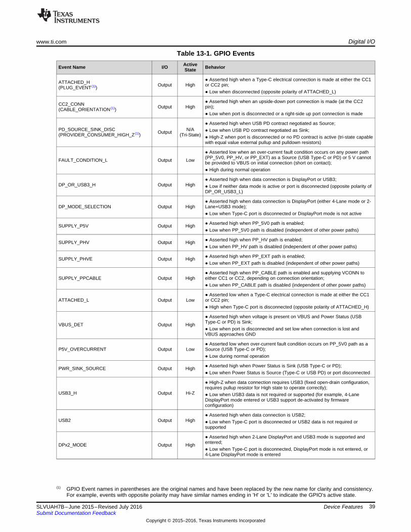
The firmware also specifies specific events that can be tied to GPIOs. These events dictate the behaviorof a specified GPIO in response to a defined hardware or USB event. The TPS65982 Configuration Toolcan be used to assign events to specific GPIOs. Table 13-1 specifies the events that are available infirmware for use with the GPIOs and their behavior.
www.ti.com Digital I/O
39SLVUAH7B–June 2015–Revised July 2016Submit Documentation Feedback
Copyright © 2015–2016, Texas Instruments Incorporated
Device Features
(1) GPIO Event names in parentheses are the original names and have been replaced by the new name for clarity and consistency.For example, events with opposite polarity may have similar names ending in 'H' or 'L' to indicate the GPIO's active state.
Table 13-1. GPIO Events
Event Name I/O ActiveState Behavior
ATTACHED_H(PLUG_EVENT (1)) Output High
● Asserted high when a Type-C electrical connection is made at either the CC1or CC2 pin;● Low when disconnected (opposite polarity of ATTACHED_L)
CC2_CONN(CABLE_ORIENTATION (1)) Output High
● Asserted high when an upside-down port connection is made (at the CC2pin);● Low when port is disconnected or a right-side up port connection is made
PD_SOURCE_SINK_DISC(PROVIDER_CONSUMER_HIGH_Z (1)) Output N/A
(Tri-State)
● Asserted high when USB PD contract negotiated as Source;● Low when USB PD contract negotiated as Sink;● High-Z when port is disconnected or no PD contract is active (tri-state capablewith equal value external pullup and pulldown resistors)
FAULT_CONDITION_L Output Low
● Asserted low when an over-current fault condition occurs on any power path(PP_5V0, PP_HV, or PP_EXT) as a Source (USB Type-C or PD) or 5 V cannotbe provided to VBUS on initial connection (short on contact);● High during normal operation
DP_OR_USB3_H Output High● Asserted high when data connection is DisplayPort or USB3;● Low if neither data mode is active or port is disconnected (opposite polarity ofDP_OR_USB3_L)
DP_MODE_SELECTION Output High● Asserted high when data connection is DisplayPort (either 4-Lane mode or 2-Lane+USB3 mode);● Low when Type-C port is disconnected or DisplayPort mode is not active
SUPPLY_P5V Output High ● Asserted high when PP_5V0 path is enabled;● Low when PP_5V0 path is disabled (independent of other power paths)
SUPPLY_PHV Output High ● Asserted high when PP_HV path is enabled;● Low when PP_HV path is disabled (independent of other power paths)
SUPPLY_PHVE Output High ● Asserted high when PP_EXT path is enabled;● Low when PP_EXT path is disabled (independent of other power paths)
SUPPLY_PPCABLE Output High● Asserted high when PP_CABLE path is enabled and supplying VCONN toeither CC1 or CC2, depending on connection orientation;● Low when PP_CABLE path is disabled (independent of other power paths)
ATTACHED_L Output Low● Asserted low when a Type-C electrical connection is made at either the CC1or CC2 pin;● High when Type-C port is disconnected (opposite polarity of ATTACHED_H)
VBUS_DET Output High
● Asserted high when voltage is present on VBUS and Power Status (USBType-C or PD) is Sink;● Low when port is disconnected and set low when connection is lost andVBUS approaches GND
P5V_OVERCURRENT Output Low● Asserted low when over-current fault condition occurs on PP_5V0 path as aSource (USB Type-C or PD);● Low during normal operation
PWR_SINK_SOURCE Output High ● Asserted high when Power Status is Sink (USB Type-C or PD);● Low when Power Status is Source (Type-C or USB PD) or port disconnected
USB3_H Output Hi-Z
● High-Z when data connection requires USB3 (fixed open-drain configuration,requires pullup resistor for High state to operate correctly);● Low when USB3 data is not required or supported (for example, 4-LaneDisplayPort mode entered or USB3 support de-activated by firmwareconfiguration)
USB2 Output High● Asserted high when data connection is USB2;● Low when Type-C port is disconnected or USB2 data is not required orsupported
DPx2_MODE Output High
● Asserted high when 2-Lane DisplayPort and USB3 mode is supported andentered;● Low when Type-C port is disconnected, DisplayPort mode is not entered, or4-Lane DisplayPort mode is entered
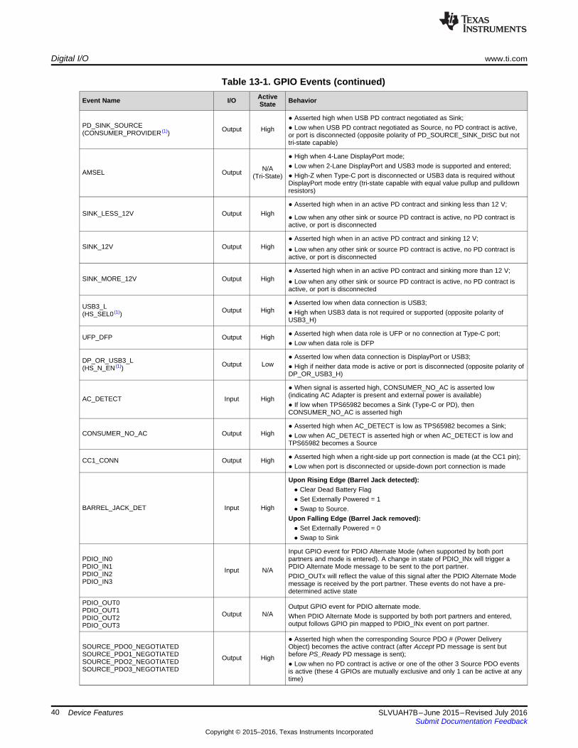
Digital I/O www.ti.com
40 SLVUAH7B–June 2015–Revised July 2016Submit Documentation Feedback
Copyright © 2015–2016, Texas Instruments Incorporated
Device Features
Table 13-1. GPIO Events (continued)
Event Name I/O ActiveState Behavior
PD_SINK_SOURCE(CONSUMER_PROVIDER (1)) Output High
● Asserted high when USB PD contract negotiated as Sink;● Low when USB PD contract negotiated as Source, no PD contract is active,or port is disconnected (opposite polarity of PD_SOURCE_SINK_DISC but nottri-state capable)
AMSEL Output N/A(Tri-State)
● High when 4-Lane DisplayPort mode;● Low when 2-Lane DisplayPort and USB3 mode is supported and entered;● High-Z when Type-C port is disconnected or USB3 data is required withoutDisplayPort mode entry (tri-state capable with equal value pullup and pulldownresistors)
SINK_LESS_12V Output High● Asserted high when in an active PD contract and sinking less than 12 V;
● Low when any other sink or source PD contract is active, no PD contract isactive, or port is disconnected
SINK_12V Output High● Asserted high when in an active PD contract and sinking 12 V;● Low when any other sink or source PD contract is active, no PD contract isactive, or port is disconnected
SINK_MORE_12V Output High● Asserted high when in an active PD contract and sinking more than 12 V;● Low when any other sink or source PD contract is active, no PD contract isactive, or port is disconnected
USB3_L(HS_SEL0 (1)) Output High
● Asserted low when data connection is USB3;● High when USB3 data is not required or supported (opposite polarity ofUSB3_H)
UFP_DFP Output High ● Asserted high when data role is UFP or no connection at Type-C port;● Low when data role is DFP
DP_OR_USB3_L(HS_N_EN (1)) Output Low
● Asserted low when data connection is DisplayPort or USB3;● High if neither data mode is active or port is disconnected (opposite polarity ofDP_OR_USB3_H)
AC_DETECT Input High
● When signal is asserted high, CONSUMER_NO_AC is asserted low(indicating AC Adapter is present and external power is available)● If low when TPS65982 becomes a Sink (Type-C or PD), thenCONSUMER_NO_AC is asserted high
CONSUMER_NO_AC Output High● Asserted high when AC_DETECT is low as TPS65982 becomes a Sink;● Low when AC_DETECT is asserted high or when AC_DETECT is low andTPS65982 becomes a Source
CC1_CONN Output High ● Asserted high when a right-side up port connection is made (at the CC1 pin);● Low when port is disconnected or upside-down port connection is made
BARREL_JACK_DET Input High
Upon Rising Edge (Barrel Jack detected):● Clear Dead Battery Flag● Set Externally Powered = 1● Swap to Source.
Upon Falling Edge (Barrel Jack removed):● Set Externally Powered = 0● Swap to Sink
PDIO_IN0PDIO_IN1PDIO_IN2PDIO_IN3
Input N/A
Input GPIO event for PDIO Alternate Mode (when supported by both portpartners and mode is entered). A change in state of PDIO_INx will trigger aPDIO Alternate Mode message to be sent to the port partner.PDIO_OUTx will reflect the value of this signal after the PDIO Alternate Modemessage is received by the port partner. These events do not have a pre-determined active state
PDIO_OUT0PDIO_OUT1PDIO_OUT2PDIO_OUT3
Output N/AOutput GPIO event for PDIO alternate mode.When PDIO Alternate Mode is supported by both port partners and entered,output follows GPIO pin mapped to PDIO_INx event on port partner.
SOURCE_PDO0_NEGOTIATEDSOURCE_PDO1_NEGOTIATEDSOURCE_PDO2_NEGOTIATEDSOURCE_PDO3_NEGOTIATED
Output High
● Asserted high when the corresponding Source PDO # (Power DeliveryObject) becomes the active contract (after Accept PD message is sent butbefore PS_Ready PD message is sent);● Low when no PD contract is active or one of the other 3 Source PDO eventsis active (these 4 GPIOs are mutually exclusive and only 1 can be active at anytime)
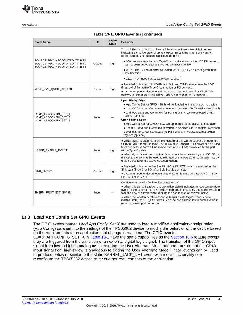
www.ti.com Load App Config Set GPIO Events
41SLVUAH7B–June 2015–Revised July 2016Submit Documentation Feedback
Copyright © 2015–2016, Texas Instruments Incorporated
Device Features
Table 13-1. GPIO Events (continued)
Event Name I/O ActiveState Behavior
SOURCE_PDO_NEGOTIATED_TT_BIT0SOURCE_PDO_NEGOTIATED_TT_BIT1SOURCE_PDO_NEGOTIATED_TT_BIT2
Output High
These 3 Events combine to form a 3-bit truth table to allow digital outputsindicating the active state of up to 7 PDOs. Bit 2 is the most-significant bit(MSB) and Bit 0 is the least significant bit (LSB)
● 000b → Indicates that the Type-C port is disconnected, a USB PD contracthas not been negotiated or a 5-V PD contract is active
● 001b-110b → The decimal equivalent of PDOx active as configured in theHost Interface
● 111b → Un-used output state (cannot occur)
VBUS_UVP_QUICK_DETECT Output High
● Asserted high when TPS65982 is a Sink and VBUS rises above the UVPthreshold of the active Type-C connection or PD contract;● Low when port is disconnected and set low immediately after VBUS fallsbelow UVP threshold of the active Type-C connection or PD contract
LOAD_APPCONFIG_SET_1LOAD_APPCONFIG_SET_2LOAD_APPCONFIG_SET_3
Input —
Upon Rising Edge:● App Config Set for GPIO = High will be loaded as the active configuration● 1st 4CC Data and Command is written to selected CMDX register (optional)● 2nd 4CC Data and Command (or PD Task) is written to selected CMDXregister (optional)
Upon Falling Edge:● App Config Set for GPIO = Low will be loaded as the active configuration● 1st 4CC Data and Command is written to selected CMDX register (optional)● 2nd 4CC Data and Command (or PD Task) is written to selected CMDXregister (optional)
USBEP_ENABLE_EVENT Input High
● When signal is asserted high, the Host Interface will be exposed through theUSB2.0 Low Speed Endpoint. The TPS65982 Endpoint (EP) driver can be usedto debug or to perform a FW update from a USB Host connected to the portwith a Type-C cable.● When signal is low the Host Interface cannot be accessed by the USB EP. Inthis case, the EP may be used to Billboard or the USB2.0 through path may beenabled based on the active data connection.
SINK_HVEXT Output High
● Asserted high when either the PP_HV or PP_EXT switch is enabled as theSink path (Type-C or PD, after Soft Start is complete;● Low when port is disconnected or any switch is enabled a Source (PP_5V0,PP_HV, or PP_EXT)
THERM_PROT_EXT_SW_IN Input —
Configurable polarity (active-high or active-low)● When this signal transitions to the active state it indicates an overtemperatureevent for the external PP_EXT switch path and immediately opens the switch tostop the flow of current while keeping the connection or contract active.● When the overtemperature event no longer exists (signal transitions toinactive state), the PP_EXT switch is closed and current flow resumes withoutrequiring a new port connection
13.3 Load App Config Set GPIO EventsThe GPIO events named Load App Config Set X are used to load a modified application-configuration(App Config) data set into the settings of the TPS65982 device to modify the behavior of the device basedon the requirements of an application that change in real-time. The GPIO eventsLOAD_APPCONFIG_SET_X in Table 13-1 have the same capabilities as the Section 10.6 feature exceptthey are triggered from the transition of an external digital-logic signal. The transition of the GPIO inputsignal from low-to-high is analogous to entering the User Alternate Mode and the transition of the GPIOinput signal from high-to-low is analogous to exiting the User Alternate Mode. These events can be usedto produce behavior similar to the static BARREL_JACK_DET event with more functionality or toreconfigure the TPS65982 device to meet other requirements of the application.
Revision History www.ti.com
42 SLVUAH7B–June 2015–Revised July 2016Submit Documentation Feedback
Copyright © 2015–2016, Texas Instruments Incorporated
Revision History
Revision HistoryNOTE: Page numbers for previous revisions may differ from page numbers in the current version.
Changes from A Revision (November 2015) to B Revision ........................................................................................... Page
• Added the TPS65981 device to the list of supported products ..................................................................... 5• Added the description of the User Alternate Mode feature......................................................................... 32• Added , deleted, and modified GPIO Events......................................................................................... 39• Added the Load App Config Set GPIO Events section ............................................................................. 41
IMPORTANT NOTICE
Texas Instruments Incorporated and its subsidiaries (TI) reserve the right to make corrections, enhancements, improvements and otherchanges to its semiconductor products and services per JESD46, latest issue, and to discontinue any product or service per JESD48, latestissue. Buyers should obtain the latest relevant information before placing orders and should verify that such information is current andcomplete. All semiconductor products (also referred to herein as “components”) are sold subject to TI’s terms and conditions of salesupplied at the time of order acknowledgment.TI warrants performance of its components to the specifications applicable at the time of sale, in accordance with the warranty in TI’s termsand conditions of sale of semiconductor products. Testing and other quality control techniques are used to the extent TI deems necessaryto support this warranty. Except where mandated by applicable law, testing of all parameters of each component is not necessarilyperformed.TI assumes no liability for applications assistance or the design of Buyers’ products. Buyers are responsible for their products andapplications using TI components. To minimize the risks associated with Buyers’ products and applications, Buyers should provideadequate design and operating safeguards.TI does not warrant or represent that any license, either express or implied, is granted under any patent right, copyright, mask work right, orother intellectual property right relating to any combination, machine, or process in which TI components or services are used. Informationpublished by TI regarding third-party products or services does not constitute a license to use such products or services or a warranty orendorsement thereof. Use of such information may require a license from a third party under the patents or other intellectual property of thethird party, or a license from TI under the patents or other intellectual property of TI.Reproduction of significant portions of TI information in TI data books or data sheets is permissible only if reproduction is without alterationand is accompanied by all associated warranties, conditions, limitations, and notices. TI is not responsible or liable for such altereddocumentation. Information of third parties may be subject to additional restrictions.Resale of TI components or services with statements different from or beyond the parameters stated by TI for that component or servicevoids all express and any implied warranties for the associated TI component or service and is an unfair and deceptive business practice.TI is not responsible or liable for any such statements.Buyer acknowledges and agrees that it is solely responsible for compliance with all legal, regulatory and safety-related requirementsconcerning its products, and any use of TI components in its applications, notwithstanding any applications-related information or supportthat may be provided by TI. Buyer represents and agrees that it has all the necessary expertise to create and implement safeguards whichanticipate dangerous consequences of failures, monitor failures and their consequences, lessen the likelihood of failures that might causeharm and take appropriate remedial actions. Buyer will fully indemnify TI and its representatives against any damages arising out of the useof any TI components in safety-critical applications.In some cases, TI components may be promoted specifically to facilitate safety-related applications. With such components, TI’s goal is tohelp enable customers to design and create their own end-product solutions that meet applicable functional safety standards andrequirements. Nonetheless, such components are subject to these terms.No TI components are authorized for use in FDA Class III (or similar life-critical medical equipment) unless authorized officers of the partieshave executed a special agreement specifically governing such use.Only those TI components which TI has specifically designated as military grade or “enhanced plastic” are designed and intended for use inmilitary/aerospace applications or environments. Buyer acknowledges and agrees that any military or aerospace use of TI componentswhich have not been so designated is solely at the Buyer's risk, and that Buyer is solely responsible for compliance with all legal andregulatory requirements in connection with such use.TI has specifically designated certain components as meeting ISO/TS16949 requirements, mainly for automotive use. In any case of use ofnon-designated products, TI will not be responsible for any failure to meet ISO/TS16949.
Products ApplicationsAudio www.ti.com/audio Automotive and Transportation www.ti.com/automotiveAmplifiers amplifier.ti.com Communications and Telecom www.ti.com/communicationsData Converters dataconverter.ti.com Computers and Peripherals www.ti.com/computersDLP® Products www.dlp.com Consumer Electronics www.ti.com/consumer-appsDSP dsp.ti.com Energy and Lighting www.ti.com/energyClocks and Timers www.ti.com/clocks Industrial www.ti.com/industrialInterface interface.ti.com Medical www.ti.com/medicalLogic logic.ti.com Security www.ti.com/securityPower Mgmt power.ti.com Space, Avionics and Defense www.ti.com/space-avionics-defenseMicrocontrollers microcontroller.ti.com Video and Imaging www.ti.com/videoRFID www.ti-rfid.comOMAP Applications Processors www.ti.com/omap TI E2E Community e2e.ti.comWireless Connectivity www.ti.com/wirelessconnectivity
Mailing Address: Texas Instruments, Post Office Box 655303, Dallas, Texas 75265Copyright © 2016, Texas Instruments Incorporated