Embed Size (px)
Citation preview
BST2
LX2
PGND2
VIN2
SW_IN
SW_OUT
FB2
COMP2COMP1
FB1
BST1
LX1
PGND1
VIN1
V7V
PGOOD1
nFAULT
SW_ENEN2
EN1
PGOOD2
VIN
PGOOD2
nFAULT
19
20
21
22
23
24
6
18 13
14
12
11
10
9
8
7
Vout1 Vout2
VIN
DVCC
TPS65283
TPS65283-1
PGOOD1
Vswout
5
1
2
3
17
Copyright © 2016, Texas Instruments Incorporated
0%
10%
20%
30%
40%
50%
60%
70%
80%
90%
100%
0.002 0.02 0.2 2
Effi
cien
cy (
%)
Loading (A)
Buck2 at 5 V
Buck1 at 1.2 V
C001
Product
Folder
Order
Now
Technical
Documents
Tools &
Software
Support &Community
An IMPORTANT NOTICE at the end of this data sheet addresses availability, warranty, changes, use in safety-critical applications,intellectual property matters and other important disclaimers. PRODUCTION DATA.
TPS65283, TPS65283-1SLVSCL3D –JUNE 2014–REVISED AUGUST 2017
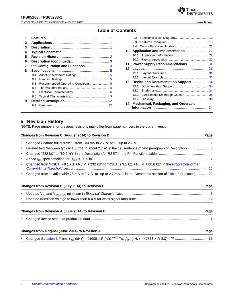
TPS65283/-1 4.5- to 18-V Input Voltage, Maximum 3.5-A/2.5-A Current, Synchronous DualBuck Converter With Power Distribution Switch
1
1 Features1• Buck Converter
– Wide Input Voltage Range 4.5 to 18 V– Integrated Dual Buck Converter, Maximum
Continuous Current 3.5 A (Buck1) / 2.5 A(Buck2)
– Feedback Reference Voltage 0.6 V ±1%– Adjustable Switching Frequency 200 kHz to
2 MHz– Internal Built Soft Start Time 2.4 ms– External Clock Synchronization– Cycle-by-Cycle Current Limit– Power Good Indicator for Each Buck– Continuous Current Mode (TPS65283) or
Pulse Skipping Mode (PSM) (TPS65283-1) atLight Load
• Power Distribution Switch– Integrated a Power Distribution Switch With
On-Resistance 60 mΩ– Operating Input Voltage Range 2.4 to 6 V– Adjustable Current Limiting up to 2.7 A– Current-Limit Accuracy ±10% at 1.25 A
(Typical)– Auto Recovery Overcurrent Protection– Reverse Input to Output Voltage Protection– Overtemperature Protection– 24-Lead VQFN (RGE) 4-mm × 4-mm Package
2 Applications• USB Ports and Hubs• Set Top Box• Digital TV• DSL/Cable Modem, Wireless Router• Home Gateway and Access Point Networks• Car Infotainment
3 DescriptionThe TPS65283, TPS65283-1 in thermally-enhanced4-mm × 4-mm VQFN package is a full featured4.5- to 18-V Vin, 3.5-A/2.5-A output currentsynchronous step down DC-DC converter, which isoptimized for small designs through high efficiencyand integrating the high-side and low-side MOSFETs.The device also incorporates one N-channelMOSFET power switches for power distributionsystems. This device provides a total powerdistribution solution, where precision current limitingand fast protection response are required.
Device Information(1)
PART NUMBER PACKAGE BODY SIZE (NOM)TPS65283
VQFN (24) 4.00 mm × 4.00 mmTPS65283-1
(1) For all available packages, see the orderable addendum atthe end of the data sheet.
4 Typical Schematic Efficiency, Vin = 12 V, PSM
2
TPS65283, TPS65283-1SLVSCL3D –JUNE 2014–REVISED AUGUST 2017 www.ti.com
Submit Documentation Feedback Copyright © 2014–2017, Texas Instruments Incorporated
Table of Contents1 Features .................................................................. 12 Applications ........................................................... 13 Description ............................................................. 14 Typical Schematic.................................................. 15 Revision History..................................................... 26 Description (continued)......................................... 37 Pin Configuration and Functions ......................... 38 Specifications......................................................... 5
8.1 Absolute Maximum Ratings ...................................... 58.2 Handling Ratings ...................................................... 58.3 Recommended Operating Conditions....................... 58.4 Thermal Information .................................................. 58.5 Electrical Characteristics........................................... 68.6 Typical Characteristics .............................................. 9
9 Detailed Description ............................................ 129.1 Overview ................................................................. 12
9.2 Functional Block Diagram ....................................... 139.3 Feature Description................................................. 139.4 Device Functional Modes........................................ 21
10 Application and Implementation........................ 2210.1 Application Information.......................................... 2210.2 Typical Application ................................................ 22
11 Power Supply Recommendations ..................... 3112 Layout................................................................... 31
12.1 Layout Guidelines ................................................. 3112.2 Layout Example .................................................... 33
13 Device and Documentation Support ................. 3413.1 Documentation Support ....................................... 3413.2 Trademarks ........................................................... 3413.3 Electrostatic Discharge Caution............................ 3413.4 Glossary ................................................................ 34
14 Mechanical, Packaging, and OrderableInformation ........................................................... 34
5 Revision HistoryNOTE: Page numbers for previous revisions may differ from page numbers in the current version.
Changes from Revision C (August 2014) to Revision D Page
• Changed Feature bullet from "...from 100 mA to 2.7 A" to "....up to 2.7 A" .......................................................................... 1• Deleted text "between typical 100 mA to about 2.7 A" in the 1st sentence of 2nd paragraph of Description. ..................... 3• Changed "232 kΩ" to "80.6 kΩ" in the Description for RSET in the Pin Functions table. ..................................................... 4• Added IOS spec condition for RSET = 80.6 kΩ ........................................................................................................................ 7• Changed from "RSET is 9.1 kΩ ≤ RLIM ≤ 232 kΩ" to "RSET is 9.1 kΩ ≤ RLIM ≤ 80.6 kΩ" in the Programming the
Current-Limit Threshold section. .......................................................................................................................................... 15• Changed from "...adjustable 75 mA to 2.7 A" to "up to 2.7 mA..." in the Comments section of Table 2 (4 places). .......... 22
Changes from Revision B (July 2014) to Revision C Page
• Updated V7V and VSYNC_LO minimum in Electrical Characteristics .......................................................................................... 6• Updated transition voltage to lower than 0.4 V for clock signal amplitude........................................................................... 17
Changes from Revision A (June 2014) to Revision B Page
• Changed device status to production data ............................................................................................................................ 1
Changes from Original (June 2014) to Revision A Page
• Changed Equation 3 From: ƒosc (kHz) = 41008 × R (kΩ)–0.979 To: ƒosc (kHz) = 47863 × R (kΩ)–0.988 .................................. 16
Thermal Pad
SW_IN
PGND2
LX2
RS
ET
BST2F
B1
AGND
1 2 3 4 5 6
7
8
9
10
11
12
CO
MP
1
17 16 15 14 1318
24
23
22
21
20
19
FB
2
CO
MP
2
VIN2
SW_OUT
PGOOD2
nFAULT
EN
1
EN
2
SW
_EN
RO
SC
/SY
NC
LX1
BST1
VIN1
PGND1
PGOOD1
V7V
3
TPS65283, TPS65283-1www.ti.com SLVSCL3D –JUNE 2014–REVISED AUGUST 2017
Submit Documentation FeedbackCopyright © 2014–2017, Texas Instruments Incorporated
6 Description (continued)The 60-mΩ independent power distribution switch limits the output current to a programmable current limitthreshold by using an external resistor. The current limit accuracy can be achieved as tight as ±10% at typical1.25 A. The nFAULT output asserts low under overcurrent and reverse-voltage conditions.
Constant frequency peak current mode control in DC-DC converter simplifies the compensation and optimizestransient response. Cycle-by-cycle overcurrent protection and operating in hiccup mode limit MOSFET powerdissipation during buck output short circuit or over loading conditions. When die temperature exceeds thermalover loading threshold, the overtemperature protection shuts down the device.
spacer
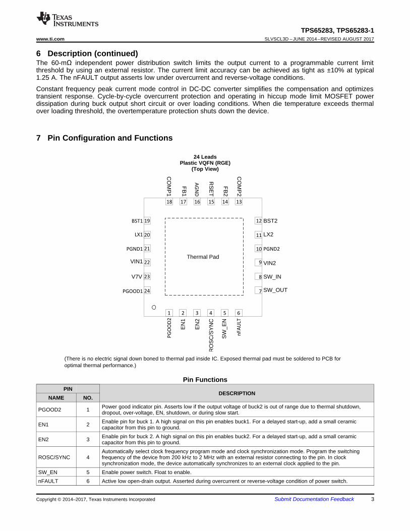
7 Pin Configuration and Functions
24 LeadsPlastic VQFN (RGE)
(Top View)
(There is no electric signal down boned to thermal pad inside IC. Exposed thermal pad must be soldered to PCB foroptimal thermal performance.)
Pin FunctionsPIN
DESCRIPTIONNAME NO.
PGOOD2 1 Power good indicator pin. Asserts low if the output voltage of buck2 is out of range due to thermal shutdown,dropout, over-voltage, EN, shutdown, or during slow start.
EN1 2 Enable pin for buck 1. A high signal on this pin enables buck1. For a delayed start-up, add a small ceramiccapacitor from this pin to ground.
EN2 3 Enable pin for buck 2. A high signal on this pin enables buck2. For a delayed start-up, add a small ceramiccapacitor from this pin to ground.
ROSC/SYNC 4Automatically select clock frequency program mode and clock synchronization mode. Program the switchingfrequency of the device from 200 kHz to 2 MHz with an external resistor connecting to the pin. In clocksynchronization mode, the device automatically synchronizes to an external clock applied to the pin.
SW_EN 5 Enable power switch. Float to enable.nFAULT 6 Active low open-drain output. Asserted during overcurrent or reverse-voltage condition of power switch.
4
TPS65283, TPS65283-1SLVSCL3D –JUNE 2014–REVISED AUGUST 2017 www.ti.com
Submit Documentation Feedback Copyright © 2014–2017, Texas Instruments Incorporated
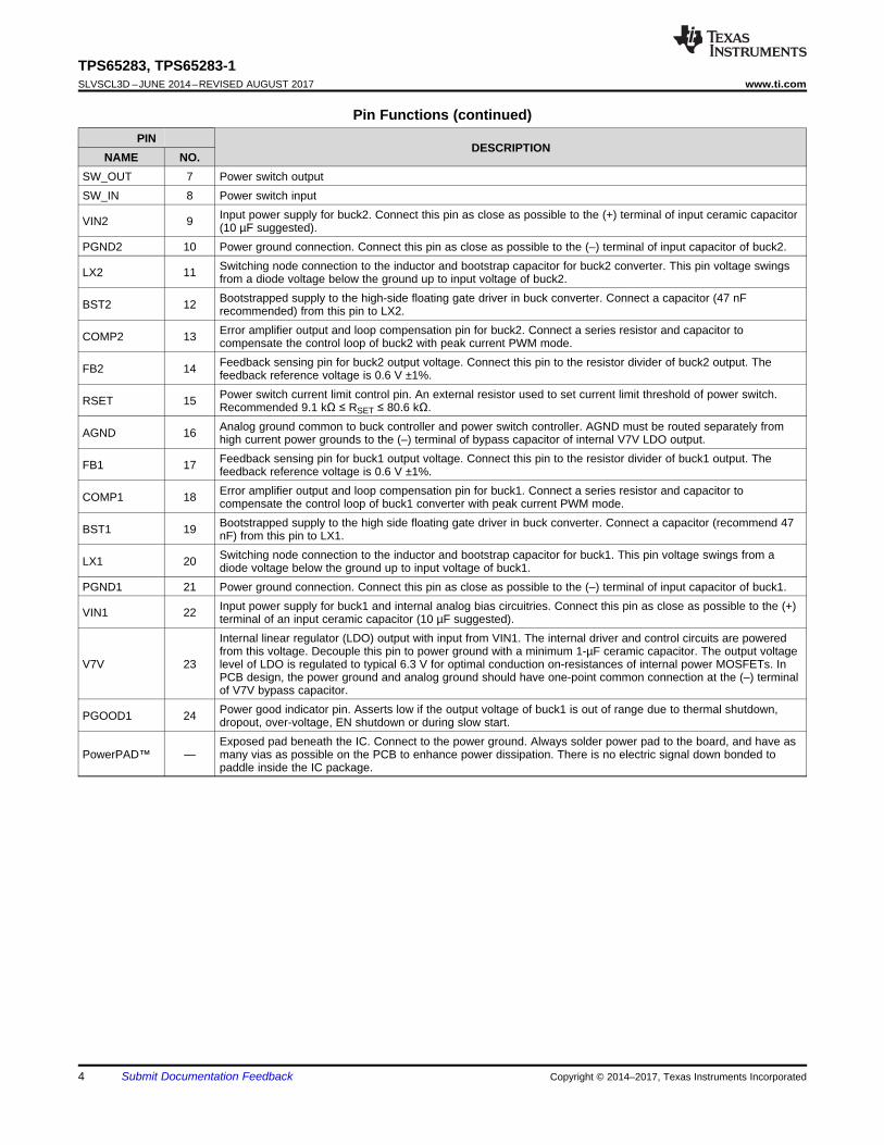
Pin Functions (continued)PIN
DESCRIPTIONNAME NO.
SW_OUT 7 Power switch outputSW_IN 8 Power switch input
VIN2 9 Input power supply for buck2. Connect this pin as close as possible to the (+) terminal of input ceramic capacitor(10 µF suggested).
PGND2 10 Power ground connection. Connect this pin as close as possible to the (–) terminal of input capacitor of buck2.
LX2 11 Switching node connection to the inductor and bootstrap capacitor for buck2 converter. This pin voltage swingsfrom a diode voltage below the ground up to input voltage of buck2.
BST2 12 Bootstrapped supply to the high-side floating gate driver in buck converter. Connect a capacitor (47 nFrecommended) from this pin to LX2.
COMP2 13 Error amplifier output and loop compensation pin for buck2. Connect a series resistor and capacitor tocompensate the control loop of buck2 with peak current PWM mode.
FB2 14 Feedback sensing pin for buck2 output voltage. Connect this pin to the resistor divider of buck2 output. Thefeedback reference voltage is 0.6 V ±1%.
RSET 15 Power switch current limit control pin. An external resistor used to set current limit threshold of power switch.Recommended 9.1 kΩ ≤ RSET ≤ 80.6 kΩ.
AGND 16 Analog ground common to buck controller and power switch controller. AGND must be routed separately fromhigh current power grounds to the (–) terminal of bypass capacitor of internal V7V LDO output.
FB1 17 Feedback sensing pin for buck1 output voltage. Connect this pin to the resistor divider of buck1 output. Thefeedback reference voltage is 0.6 V ±1%.
COMP1 18 Error amplifier output and loop compensation pin for buck1. Connect a series resistor and capacitor tocompensate the control loop of buck1 converter with peak current PWM mode.
BST1 19 Bootstrapped supply to the high side floating gate driver in buck converter. Connect a capacitor (recommend 47nF) from this pin to LX1.
LX1 20 Switching node connection to the inductor and bootstrap capacitor for buck1. This pin voltage swings from adiode voltage below the ground up to input voltage of buck1.
PGND1 21 Power ground connection. Connect this pin as close as possible to the (–) terminal of input capacitor of buck1.
VIN1 22 Input power supply for buck1 and internal analog bias circuitries. Connect this pin as close as possible to the (+)terminal of an input ceramic capacitor (10 µF suggested).
V7V 23
Internal linear regulator (LDO) output with input from VIN1. The internal driver and control circuits are poweredfrom this voltage. Decouple this pin to power ground with a minimum 1-µF ceramic capacitor. The output voltagelevel of LDO is regulated to typical 6.3 V for optimal conduction on-resistances of internal power MOSFETs. InPCB design, the power ground and analog ground should have one-point common connection at the (–) terminalof V7V bypass capacitor.
PGOOD1 24 Power good indicator pin. Asserts low if the output voltage of buck1 is out of range due to thermal shutdown,dropout, over-voltage, EN shutdown or during slow start.
PowerPAD™ —Exposed pad beneath the IC. Connect to the power ground. Always solder power pad to the board, and have asmany vias as possible on the PCB to enhance power dissipation. There is no electric signal down bonded topaddle inside the IC package.
5
TPS65283, TPS65283-1www.ti.com SLVSCL3D –JUNE 2014–REVISED AUGUST 2017
Submit Documentation FeedbackCopyright © 2014–2017, Texas Instruments Incorporated
(1) Stresses beyond those listed under Absolute Maximum Ratings may cause permanent damage to the device. These are stress ratingsonly, which do not imply functional operation of the device at these or any other conditions beyond those indicated under RecommendedOperating Conditions. Exposure to absolute-maximum-rated conditions for extended periods may affect device reliability.
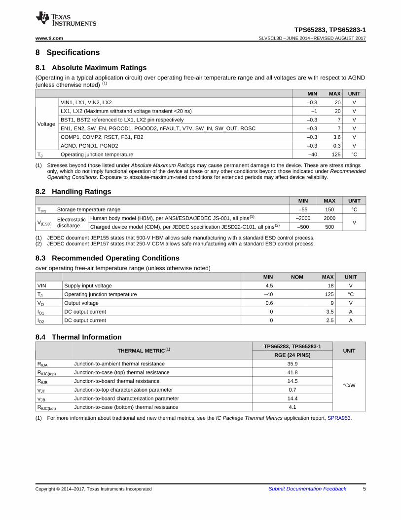
8 Specifications
8.1 Absolute Maximum Ratings(Operating in a typical application circuit) over operating free-air temperature range and all voltages are with respect to AGND(unless otherwise noted) (1)
MIN MAX UNIT
Voltage
VIN1, LX1, VIN2, LX2 –0.3 20 VLX1, LX2 (Maximum withstand voltage transient <20 ns) –1 20 VBST1, BST2 referenced to LX1, LX2 pin respectively –0.3 7 VEN1, EN2, SW_EN, PGOOD1, PGOOD2, nFAULT, V7V, SW_IN, SW_OUT, ROSC –0.3 7 VCOMP1, COMP2, RSET, FB1, FB2 –0.3 3.6 VAGND, PGND1, PGND2 –0.3 0.3 V
TJ Operating junction temperature –40 125 °C
(1) JEDEC document JEP155 states that 500-V HBM allows safe manufacturing with a standard ESD control process.(2) JEDEC document JEP157 states that 250-V CDM allows safe manufacturing with a standard ESD control process.
8.2 Handling RatingsMIN MAX UNIT
Tstg Storage temperature range –55 150 °C
V(ESD)Electrostaticdischarge
Human body model (HBM), per ANSI/ESDA/JEDEC JS-001, all pins (1) –2000 2000V
Charged device model (CDM), per JEDEC specification JESD22-C101, all pins (2) –500 500
8.3 Recommended Operating Conditionsover operating free-air temperature range (unless otherwise noted)
MIN NOM MAX UNITVIN Supply input voltage 4.5 18 VTJ Operating junction temperature –40 125 °CVO Output voltage 0.6 9 VIO1 DC output current 0 3.5 AIO2 DC output current 0 2.5 A
(1) For more information about traditional and new thermal metrics, see the IC Package Thermal Metrics application report, SPRA953.
8.4 Thermal Information
THERMAL METRIC (1) TPS65283, TPS65283-1UNIT
RGE (24 PINS)RθJA Junction-to-ambient thermal resistance 35.9
°C/W
RθJC(top) Junction-to-case (top) thermal resistance 41.8RθJB Junction-to-board thermal resistance 14.5ψJT Junction-to-top characterization parameter 0.7ψJB Junction-to-board characterization parameter 14.4RθJC(bot) Junction-to-case (bottom) thermal resistance 4.1
6
TPS65283, TPS65283-1SLVSCL3D –JUNE 2014–REVISED AUGUST 2017 www.ti.com
Submit Documentation Feedback Copyright © 2014–2017, Texas Instruments Incorporated
(1) Specified by design.
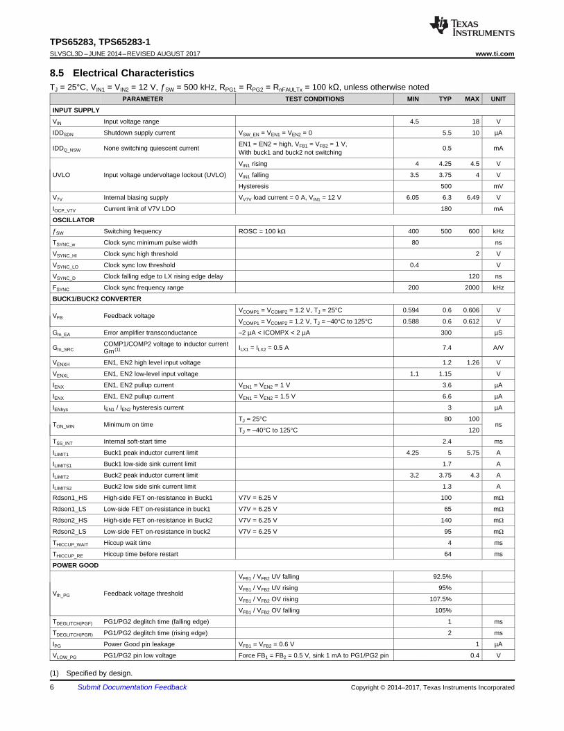
8.5 Electrical CharacteristicsTJ = 25°C, VIN1 = VIN2 = 12 V, ƒSW = 500 kHz, RPG1 = RPG2 = RnFAULTx = 100 kΩ, unless otherwise noted
PARAMETER TEST CONDITIONS MIN TYP MAX UNIT
INPUT SUPPLY
VIN Input voltage range 4.5 18 V
IDDSDN Shutdown supply current VSW_EN = VEN1 = VEN2 = 0 5.5 10 µA
IDDQ_NSW None switching quiescent current EN1 = EN2 = high, VFB1 = VFB2 = 1 V,With buck1 and buck2 not switching 0.5 mA
UVLO Input voltage undervoltage lockout (UVLO)
VIN1 rising 4 4.25 4.5 V
VIN1 falling 3.5 3.75 4 V
Hysteresis 500 mV
V7V Internal biasing supply VV7V load current = 0 A, VIN1 = 12 V 6.05 6.3 6.49 V
IOCP_V7V Current limit of V7V LDO 180 mA
OSCILLATOR
ƒSW Switching frequency ROSC = 100 kΩ 400 500 600 kHz
TSYNC_w Clock sync minimum pulse width 80 ns
VSYNC_HI Clock sync high threshold 2 V
VSYNC_LO Clock sync low threshold 0.4 V
VSYNC_D Clock falling edge to LX rising edge delay 120 ns
FSYNC Clock sync frequency range 200 2000 kHz
BUCK1/BUCK2 CONVERTER
VFB Feedback voltageVCOMP1 = VCOMP2 = 1.2 V, TJ = 25°C 0.594 0.6 0.606 V
VCOMP1 = VCOMP2 = 1.2 V, TJ = –40°C to 125°C 0.588 0.6 0.612 V
Gm_EA Error amplifier transconductance –2 µA < ICOMPX < 2 µA 300 µS
Gm_SRCCOMP1/COMP2 voltage to inductor currentGm (1) ILX1 = ILX2 = 0.5 A 7.4 A/V
VENXH EN1, EN2 high level input voltage 1.2 1.26 V
VENXL EN1, EN2 low-level input voltage 1.1 1.15 V
IENX EN1, EN2 pullup current VEN1 = VEN2 = 1 V 3.6 µA
IENX EN1, EN2 pullup current VEN1 = VEN2 = 1.5 V 6.6 µA
IENhys IEN1 / IEN2 hysteresis current 3 µA
TON_MIN Minimum on timeTJ = 25°C 80 100
nsTJ = –40°C to 125°C 120
TSS_INT Internal soft-start time 2.4 ms
ILIMIT1 Buck1 peak inductor current limit 4.25 5 5.75 A
ILIMITS1 Buck1 low-side sink current limit 1.7 A
ILIMIT2 Buck2 peak inductor current limit 3.2 3.75 4.3 A
ILIMITS2 Buck2 low side sink current limit 1.3 A
Rdson1_HS High-side FET on-resistance in Buck1 V7V = 6.25 V 100 mΩ
Rdson1_LS Low-side FET on-resistance in buck1 V7V = 6.25 V 65 mΩ
Rdson2_HS High-side FET on-resistance in Buck2 V7V = 6.25 V 140 mΩ
Rdson2_LS Low-side FET on-resistance in buck2 V7V = 6.25 V 95 mΩ
THICCUP_WAIT Hiccup wait time 4 ms
THICCUP_RE Hiccup time before restart 64 ms
POWER GOOD
Vth_PG Feedback voltage threshold
VFB1 / VFB2 UV falling 92.5%
VFB1 / VFB2 UV rising 95%
VFB1 / VFB2 OV rising 107.5%
VFB1 / VFB2 OV falling 105%
TDEGLITCH(PGF) PG1/PG2 deglitch time (falling edge) 1 ms
TDEGLITCH(PGR) PG1/PG2 deglitch time (rising edge) 2 ms
IPG Power Good pin leakage VFB1 = VFB2 = 0.6 V 1 µA
VLOW_PG PG1/PG2 pin low voltage Force FB1 = FB2 = 0.5 V, sink 1 mA to PG1/PG2 pin 0.4 V
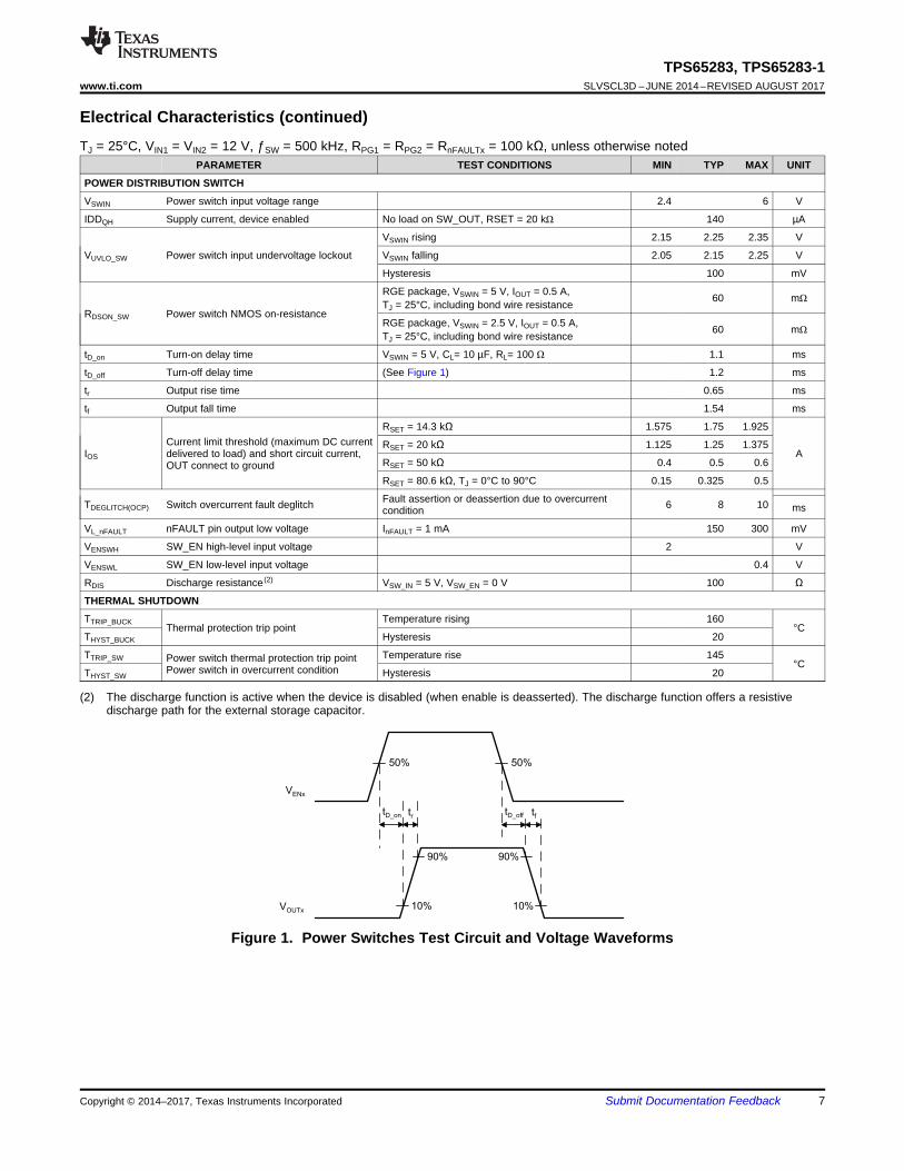
VENx
VOUTx
tD_on
90%
10%
50% 50%
90%
tD_off
10%
tr tf
7
TPS65283, TPS65283-1www.ti.com SLVSCL3D –JUNE 2014–REVISED AUGUST 2017
Submit Documentation FeedbackCopyright © 2014–2017, Texas Instruments Incorporated
Electrical Characteristics (continued)TJ = 25°C, VIN1 = VIN2 = 12 V, ƒSW = 500 kHz, RPG1 = RPG2 = RnFAULTx = 100 kΩ, unless otherwise noted
PARAMETER TEST CONDITIONS MIN TYP MAX UNIT
(2) The discharge function is active when the device is disabled (when enable is deasserted). The discharge function offers a resistivedischarge path for the external storage capacitor.
POWER DISTRIBUTION SWITCH
VSWIN Power switch input voltage range 2.4 6 V
IDDQH Supply current, device enabled No load on SW_OUT, RSET = 20 kΩ 140 µA
VUVLO_SW Power switch input undervoltage lockout
VSWIN rising 2.15 2.25 2.35 V
VSWIN falling 2.05 2.15 2.25 V
Hysteresis 100 mV
RDSON_SW Power switch NMOS on-resistance
RGE package, VSWIN = 5 V, IOUT = 0.5 A,TJ = 25°C, including bond wire resistance 60 mΩ
RGE package, VSWIN = 2.5 V, IOUT = 0.5 A,TJ = 25°C, including bond wire resistance 60 mΩ
tD_on Turn-on delay time VSWIN = 5 V, CL= 10 µF, RL= 100 Ω 1.1 ms
tD_off Turn-off delay time (See Figure 1) 1.2 ms
tr Output rise time 0.65 ms
tf Output fall time 1.54 ms
IOS
Current limit threshold (maximum DC currentdelivered to load) and short circuit current,OUT connect to ground
RSET = 14.3 kΩ 1.575 1.75 1.925
ARSET = 20 kΩ 1.125 1.25 1.375
RSET = 50 kΩ 0.4 0.5 0.6
RSET = 80.6 kΩ, TJ = 0°C to 90°C 0.15 0.325 0.5
TDEGLITCH(OCP) Switch overcurrent fault deglitch Fault assertion or deassertion due to overcurrentcondition 6 8 10 ms
VL_nFAULT nFAULT pin output low voltage InFAULT = 1 mA 150 300 mV
VENSWH SW_EN high-level input voltage 2 V
VENSWL SW_EN low-level input voltage 0.4 V
RDIS Discharge resistance (2) VSW_IN = 5 V, VSW_EN = 0 V 100 Ω
THERMAL SHUTDOWN
TTRIP_BUCKThermal protection trip point
Temperature rising 160°C
THYST_BUCK Hysteresis 20
TTRIP_SW Power switch thermal protection trip pointPower switch in overcurrent condition
Temperature rise 145°C
THYST_SW Hysteresis 20
Figure 1. Power Switches Test Circuit and Voltage Waveforms
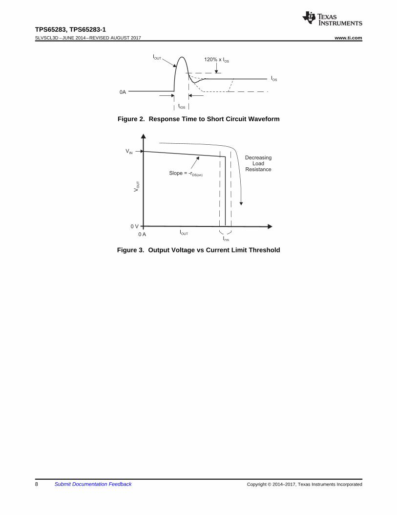
DecreasingLoad
ResistanceSlope = -rDS(on)
VIN
0 V
0 A IOUT
VO
UT
IOS
120% x IOS
IOUT
IOS
tIOS
0A
8
TPS65283, TPS65283-1SLVSCL3D –JUNE 2014–REVISED AUGUST 2017 www.ti.com
Submit Documentation Feedback Copyright © 2014–2017, Texas Instruments Incorporated
Figure 2. Response Time to Short Circuit Waveform
Figure 3. Output Voltage vs Current Limit Threshold
1.2
1.2
1.2
1.2
1.2
1.2
1.2
1.2
1.2
1.2
1.3
0.0 0.5 1.0 1.5 2.0 2.5 3.0 3.5
VO
UT
(V
)
Loading (A)
Auto PSM-PWM 0A
Forced PWM 2A
C009
4.95
4.96
4.97
4.98
4.99
5.00
5.01
5.02
5.03
5.04
5.05
0.0 0.5 1.0 1.5 2.0 2.5
VO
UT
(V
)
Loading (A)
Auto PSM-PWM 0A
Forced PWM 2A
C008
0%
10%
20%
30%
40%
50%
60%
70%
80%
90%
100%
0.002 0.02 0.2 2
Effi
cien
cy (
%)
Loading (A)
9 V
12 V
18 V
C003
0%
10%
20%
30%
40%
50%
60%
70%
80%
90%
100%
0.002 0.02 0.2 2
Effi
cien
cy (
%)
Loading (A)
9 V
12 V
18 V
C003
0%
10%
20%
30%
40%
50%
60%
70%
80%
90%
100%
0.002 0.02 0.2 2
Effi
cien
cy (
%)
Loading (A)
9 V
12 V
18 V
C002
0%
10%
20%
30%
40%
50%
60%
70%
80%
90%
100%
0.002 0.02 0.2 2
Effi
cien
cy (
%)
Loading (A)
9 V
12 V
18 V
C003
9
TPS65283, TPS65283-1www.ti.com SLVSCL3D –JUNE 2014–REVISED AUGUST 2017
Submit Documentation FeedbackCopyright © 2014–2017, Texas Instruments Incorporated
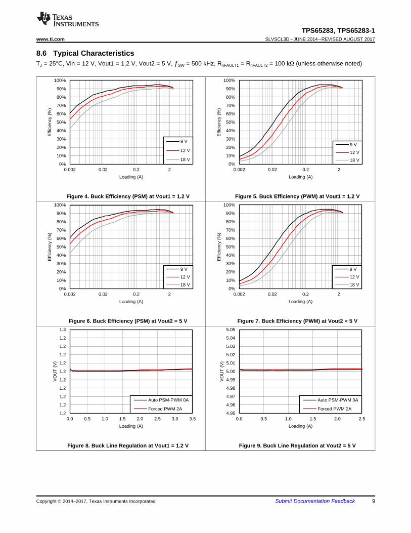
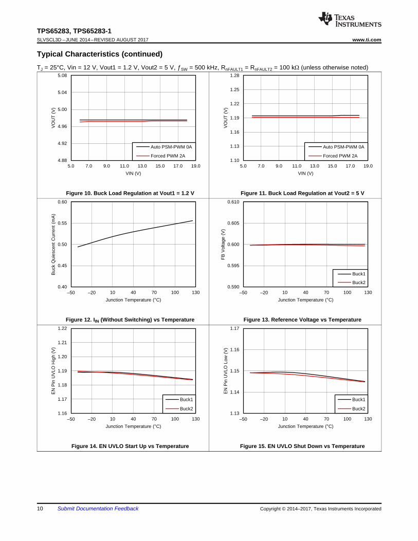
8.6 Typical CharacteristicsTJ = 25°C, Vin = 12 V, Vout1 = 1.2 V, Vout2 = 5 V, ƒSW = 500 kHz, RnFAULT1 = RnFAULT2 = 100 kΩ (unless otherwise noted)
Figure 4. Buck Efficiency (PSM) at Vout1 = 1.2 V Figure 5. Buck Efficiency (PWM) at Vout1 = 1.2 V
Figure 6. Buck Efficiency (PSM) at Vout2 = 5 V Figure 7. Buck Efficiency (PWM) at Vout2 = 5 V
Figure 8. Buck Line Regulation at Vout1 = 1.2 V Figure 9. Buck Line Regulation at Vout2 = 5 V
1.16
1.17
1.18
1.19
1.20
1.21
1.22
±50 ±20 10 40 70 100 130
EN
Pin
UV
LO H
igh
(V)
Junction Temperature (C)
Buck1
Buck2
C023
1.13
1.14
1.15
1.16
1.17
±50 ±20 10 40 70 100 130
EN
Pin
UV
LO L
ow (
V)
Junction Temperature (C)
Buck1
Buck2
C023
0.40
0.45
0.50
0.55
0.60
±50 ±20 10 40 70 100 130
Buc
k Q
uies
cent
Cur
rent
(m
A)
Junction Temperature (C) C013
0.590
0.595
0.600
0.605
0.610
±50 ±20 10 40 70 100 130
FB
Vol
tage
(V
)
Junction Temperature (C)
Buck1
Buck2
C014
4.88
4.92
4.96
5.00
5.04
5.08
5.0 7.0 9.0 11.0 13.0 15.0 17.0 19.0
VO
UT
(V
)
VIN (V)
Auto PSM-PWM 0A
Forced PWM 2A
C006
1.10
1.13
1.16
1.19
1.22
1.25
1.28
5.0 7.0 9.0 11.0 13.0 15.0 17.0 19.0
VO
UT
(V
)
VIN (V)
Auto PSM-PWM 0A
Forced PWM 2A
C007
10
TPS65283, TPS65283-1SLVSCL3D –JUNE 2014–REVISED AUGUST 2017 www.ti.com
Submit Documentation Feedback Copyright © 2014–2017, Texas Instruments Incorporated
Typical Characteristics (continued)TJ = 25°C, Vin = 12 V, Vout1 = 1.2 V, Vout2 = 5 V, ƒSW = 500 kHz, RnFAULT1 = RnFAULT2 = 100 kΩ (unless otherwise noted)
Figure 10. Buck Load Regulation at Vout1 = 1.2 V Figure 11. Buck Load Regulation at Vout2 = 5 V
Figure 12. IIN (Without Switching) vs Temperature Figure 13. Reference Voltage vs Temperature
Figure 14. EN UVLO Start Up vs Temperature Figure 15. EN UVLO Shut Down vs Temperature

1.15
1.20
1.25
1.30
1.35
±50 ±20 10 40 70 100 130
Pow
er S
witc
h O
C (
A)
Environment Temperature (C) C021
0
20
40
60
80
100
120
0 1 2 3 4 5 6 7 8 9
Res
pons
e T
ime
(us)
Current (A) C022
50
60
70
80
90
±50 ±20 10 40 70 100 130
Min
imum
On
Tim
e (n
s)
Junction Temperature (C)
Buck1
Buck2
C019
0.120
0.125
0.130
0.135
0.140
0.145
0.150
±50 ±20 10 40 70 100 130
Pow
er S
witc
h Q
uies
cent
Cur
rent
(m
A)
Junction Temperature (C) C020
4.7
4.8
4.9
5.0
5.1
±50 ±30 ±10 10 30 50 70 90 110 130
Buc
k1 C
urre
nt L
imit
(A)
Junction Temperature (C) C017
3.45
3.55
3.65
3.75
3.85
±50 ±30 ±10 10 30 50 70 90 110 130
Buc
k2 C
urre
nt L
imit
(A)
Junction Temperature (C) C017
11
TPS65283, TPS65283-1www.ti.com SLVSCL3D –JUNE 2014–REVISED AUGUST 2017
Submit Documentation FeedbackCopyright © 2014–2017, Texas Instruments Incorporated
Typical Characteristics (continued)TJ = 25°C, Vin = 12 V, Vout1 = 1.2 V, Vout2 = 5 V, ƒSW = 500 kHz, RnFAULT1 = RnFAULT2 = 100 kΩ (unless otherwise noted)
Figure 16. Buck1 Current Limit vs Temperature Figure 17. Buck2 Current Limit vs Temperature
Figure 18. Buck Minimum On Time vs Temperature Figure 19. Supply Current (Switch Enabled) vs Temperature
Figure 20. Switch Current Limit vs Temperature(Rset = 20 kΩ)
Figure 21. Response Time vs SW_OUT Current
12
TPS65283, TPS65283-1SLVSCL3D –JUNE 2014–REVISED AUGUST 2017 www.ti.com
Submit Documentation Feedback Copyright © 2014–2017, Texas Instruments Incorporated
9 Detailed Description
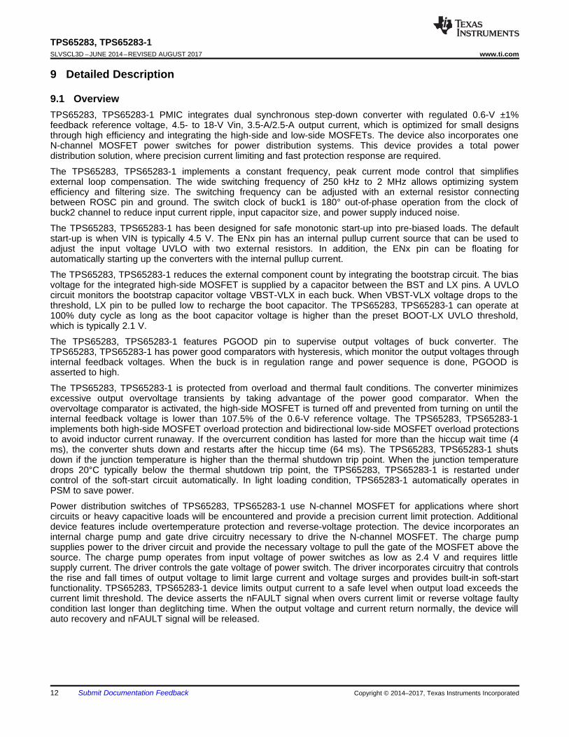
9.1 OverviewTPS65283, TPS65283-1 PMIC integrates dual synchronous step-down converter with regulated 0.6-V ±1%feedback reference voltage, 4.5- to 18-V Vin, 3.5-A/2.5-A output current, which is optimized for small designsthrough high efficiency and integrating the high-side and low-side MOSFETs. The device also incorporates oneN-channel MOSFET power switches for power distribution systems. This device provides a total powerdistribution solution, where precision current limiting and fast protection response are required.
The TPS65283, TPS65283-1 implements a constant frequency, peak current mode control that simplifiesexternal loop compensation. The wide switching frequency of 250 kHz to 2 MHz allows optimizing systemefficiency and filtering size. The switching frequency can be adjusted with an external resistor connectingbetween ROSC pin and ground. The switch clock of buck1 is 180° out-of-phase operation from the clock ofbuck2 channel to reduce input current ripple, input capacitor size, and power supply induced noise.
The TPS65283, TPS65283-1 has been designed for safe monotonic start-up into pre-biased loads. The defaultstart-up is when VIN is typically 4.5 V. The ENx pin has an internal pullup current source that can be used toadjust the input voltage UVLO with two external resistors. In addition, the ENx pin can be floating forautomatically starting up the converters with the internal pullup current.
The TPS65283, TPS65283-1 reduces the external component count by integrating the bootstrap circuit. The biasvoltage for the integrated high-side MOSFET is supplied by a capacitor between the BST and LX pins. A UVLOcircuit monitors the bootstrap capacitor voltage VBST-VLX in each buck. When VBST-VLX voltage drops to thethreshold, LX pin to be pulled low to recharge the boot capacitor. The TPS65283, TPS65283-1 can operate at100% duty cycle as long as the boot capacitor voltage is higher than the preset BOOT-LX UVLO threshold,which is typically 2.1 V.
The TPS65283, TPS65283-1 features PGOOD pin to supervise output voltages of buck converter. TheTPS65283, TPS65283-1 has power good comparators with hysteresis, which monitor the output voltages throughinternal feedback voltages. When the buck is in regulation range and power sequence is done, PGOOD isasserted to high.
The TPS65283, TPS65283-1 is protected from overload and thermal fault conditions. The converter minimizesexcessive output overvoltage transients by taking advantage of the power good comparator. When theovervoltage comparator is activated, the high-side MOSFET is turned off and prevented from turning on until theinternal feedback voltage is lower than 107.5% of the 0.6-V reference voltage. The TPS65283, TPS65283-1implements both high-side MOSFET overload protection and bidirectional low-side MOSFET overload protectionsto avoid inductor current runaway. If the overcurrent condition has lasted for more than the hiccup wait time (4ms), the converter shuts down and restarts after the hiccup time (64 ms). The TPS65283, TPS65283-1 shutsdown if the junction temperature is higher than the thermal shutdown trip point. When the junction temperaturedrops 20°C typically below the thermal shutdown trip point, the TPS65283, TPS65283-1 is restarted undercontrol of the soft-start circuit automatically. In light loading condition, TPS65283-1 automatically operates inPSM to save power.
Power distribution switches of TPS65283, TPS65283-1 use N-channel MOSFET for applications where shortcircuits or heavy capacitive loads will be encountered and provide a precision current limit protection. Additionaldevice features include overtemperature protection and reverse-voltage protection. The device incorporates aninternal charge pump and gate drive circuitry necessary to drive the N-channel MOSFET. The charge pumpsupplies power to the driver circuit and provide the necessary voltage to pull the gate of the MOSFET above thesource. The charge pump operates from input voltage of power switches as low as 2.4 V and requires littlesupply current. The driver controls the gate voltage of power switch. The driver incorporates circuitry that controlsthe rise and fall times of output voltage to limit large current and voltage surges and provides built-in soft-startfunctionality. TPS65283, TPS65283-1 device limits output current to a safe level when output load exceeds thecurrent limit threshold. The device asserts the nFAULT signal when overs current limit or reverse voltage faultycondition last longer than deglitching time. When the output voltage and current return normally, the device willauto recovery and nFAULT signal will be released.
DriverCurrent
Limit
CS
Charge Pump
UVLOPOR
8-ms Deglitch
TimeEnable Buffer
Current Sensing
1.25 M
7SW_OUT
nFAULT6
5SW_EN
SW_IN8
10PGND2
VIN29
16AGND
15RSET
POWER SWITCH
2EN1
VIN122
LX120
PGND121
17FB1
18COMP1
0.6V2.4-ms Internal
Soft Start
Current Sensing
CS
HS current sensing
CSLS current sensing
Voltage Reference Current Bias
LDO
BST119
V7V
Preregulator
Buck Controller
23V7V
Enable Comparator
Oscillotor
4ROSC/SYNC
10 µA
24 PGOOD1
Error Amplifier
PWM comparator
HS driver
LS driverslope comp
5V
1.25 M
0.645 V
0.555 V
BUCK2
BUCK1
EN2
COMP2
FB2
PGOOD21
14
13
3
BST2
LX2
12
11
Enable Threshold
Thermal Sense
Disabled + UVLO
BST Switch
V7V
Copyright © 2017, Texas Instruments Incorporated
13
TPS65283, TPS65283-1www.ti.com SLVSCL3D –JUNE 2014–REVISED AUGUST 2017
Submit Documentation FeedbackCopyright © 2014–2017, Texas Instruments Incorporated
9.2 Functional Block Diagram
9.3 Feature Description
9.3.1 Power Switch Detailed Description
9.3.1.1 Overcurrent ConditionThe TPS65283, TPS65283-1 responds to overcurrent conditions on power switches by limiting the outputcurrents to IOCP_SW level, which is set by external resistor. When the load current is less than the current-limitthreshold, the devices are not limiting current. During normal operation, the N-channel MOSFET is fullyenhanced, and VSW_OUT = VSW_IN – (ISW_OUT × Rdson_SW). The voltage drop across the MOSFET is relatively smallcompared to VSW_IN, and VSW_OUT ≈ VSW_IN. When an overcurrent condition is detected, the device maintains aconstant output current and reduces the output voltage accordingly. During current-limit operation, the N-channelMOSFET is no longer fully enhanced and the resistance of the device increases. This allows the device to
14
TPS65283, TPS65283-1SLVSCL3D –JUNE 2014–REVISED AUGUST 2017 www.ti.com
Submit Documentation Feedback Copyright © 2014–2017, Texas Instruments Incorporated
Feature Description (continued)effectively regulate the current to the current-limit threshold. The effect of increasing the resistance of theMOSFET is that the voltage drop across the device is no longer negligible (VSW_IN ≠ VSW_OUT), and VSW_OUTdecreases. The amount that VSW_OUT decreases is proportional to the magnitude of the overload condition. Theexpected VSW_OUT can be calculated by IOCP_SW × RLOAD, where IOCP_SW is the current-limit threshold and RLOADis the magnitude of the overload condition.
Table 1 shows three possible overload conditions that can occur.
Table 1. Overload ConditionsCONDITIONS BEHAVIORS
Short circuit or partial shortcircuit present when thedevice is powered up orenabled
The output voltage is held near zero potential with respect to ground and the TPS65283, TPS65283-1ramps output current to IOCP_SW. The device limits the current to IOS until the overload condition isremoved or the internal deglitch time (8 ms typical) is reached and the device is turned off. The device autorecovers when the overcurrent status is removed.
Gradually increasing load(<100 A/s) from normaloperating current to IOCP_SW
The current rises until current limit. After the threshold has been reached, the device switches into itscurrent limiting at IOCP_SW. The device limits the current to IOS until the overload condition is removed orthe internal deglitch time (8 ms typical) is reached and the device is turned off. The device auto recoverswhen the overcurrent status is removed.
Short circuit, partial shortcircuit or fast transientoverload occurs while thedevice is enabled andpowered on
The device responds to the overcurrent condition within time TIOS (see Figure 3).The current sensingamplifier is overdriven during this time, and needs time for loop response. After TIOS has passed, thecurrent sensing amplifier recovers and limits the current to IOCP_SW. The device limits the current to IOSuntil the overload condition is removed or the internal deglitch time (8 ms typical) is reached and the deviceis turned off. The device auto recovers when the overcurrent status is removed.
9.3.1.2 Reverse Current and Voltage ProtectionThe power switch in TPS65283, TPS65283-1 incorporates one N-channel power MOSFETs for lower resistanceand the bulk of the MOSFET is connected to ground to prevent the reverse current flowing back the inputthrough body diode of MOSFET when power switch is off.
When power switch is enabled, the reverse-voltage protection feature turns off the N-channel MOSFETwhenever the output voltage exceeds the input voltage by 55 mV (typical) for 4-ms (typical). This preventsdamage to devices on the input side of the TPS65283, TPS65283-1 by preventing significant current from sinkinginto the input capacitance of power switch or buck output capacitance. The TPS65283, TPS65283-1 devicekeeps the power switch turned off even if the reverse-voltage condition is removed and does not allow the N-channel MOSFET to turn on until power is cycled or the device enable is toggled. The reverse-voltagecomparator also asserts the nFAULT output (active-low) after 4 ms.
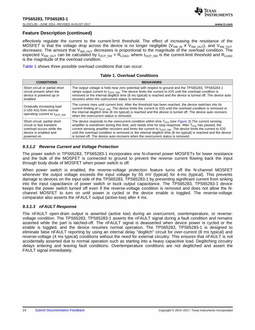
9.3.1.3 nFAULT ResponseThe nFAULT open-drain output is asserted (active low) during an overcurrent, overtemperature, or reverse-voltage condition. The TPS65283, TPS65283-1 asserts the nFAULT signal during a fault condition and remainsasserted while the part is latched-off. The nFAULT signal is deasserted when device power is cycled or theenable is toggled, and the device resumes normal operation. The TPS65283, TPS65283-1 is designed toeliminate false nFAULT reporting by using an internal delay "deglitch" circuit for over-current (8 ms typical) andreverse-voltage (4 ms typical) conditions without the need for external circuitry. This ensures that nFAULT is notaccidentally asserted due to normal operation such as starting into a heavy capacitive load. Deglitching circuitrydelays entering and leaving fault conditions. Overtemperature conditions are not deglitched and assert theFAULT signal immediately.
USB_VIN
USB_EN
tdeglitch
Over current at the outputAlarm is asserted after 8 ms
0
USB_OUT
tdeglitch
USB_I
nFAULT
Normal operation Alarm is cleared Normal operation is restored
Over current is detected Over current is cleared
Ios
15
TPS65283, TPS65283-1www.ti.com SLVSCL3D –JUNE 2014–REVISED AUGUST 2017
Submit Documentation FeedbackCopyright © 2014–2017, Texas Instruments Incorporated
Figure 22. USB Switches Over Current
9.3.1.4 UVLOThe UVLO circuit disables the power switch until the input voltage reaches the UVLO turn-on threshold. Built-inhysteresis prevents unwanted on/off cycling due to input voltage drop from large current surges.
9.3.1.5 Enable and Output DischargeThe logic enable EN_SW controls the power switch, bias for the charge pump, driver, and other circuits. Thesupply current from power switch driver is reduced to less than 1 µA when a logic low is present on EN_SW. Alogic high input on EN_SW enables the driver, control circuits, and power switch. The enable input is compatiblewith both TTL and CMOS logic levels.
When enable is deasserted, the discharge function is active. The output capacitor of power switch is dischargedthrough an internal NMOS that has a discharge resistance of 100 Ω. Hence, the output voltage drops down to 0.The time taken for discharge depends on the RC time constant of the resistance and the output capacitor.
9.3.1.6 Power Switch Input and Output CapacitanceInput and output capacitance improves the performance of the device. The actual capacitance should beoptimized for the particular application. TI recommends to place the output capacitor in buck converter betweenSW_IN and AGND as close to the device as possible for local noise decoupling. Additional capacitance may beneeded on the input to reduce voltage overshoot from exceeding the absolute maximum voltage of the deviceduring heavy transient conditions. This is especially important during bench testing when long, inductive cablesare used to connect the input of power switches in the evaluation board to the bench power-supply. TIrecommends placing a high-value electrolytic capacitor on the output pin when large transient currents areexpected on the output.
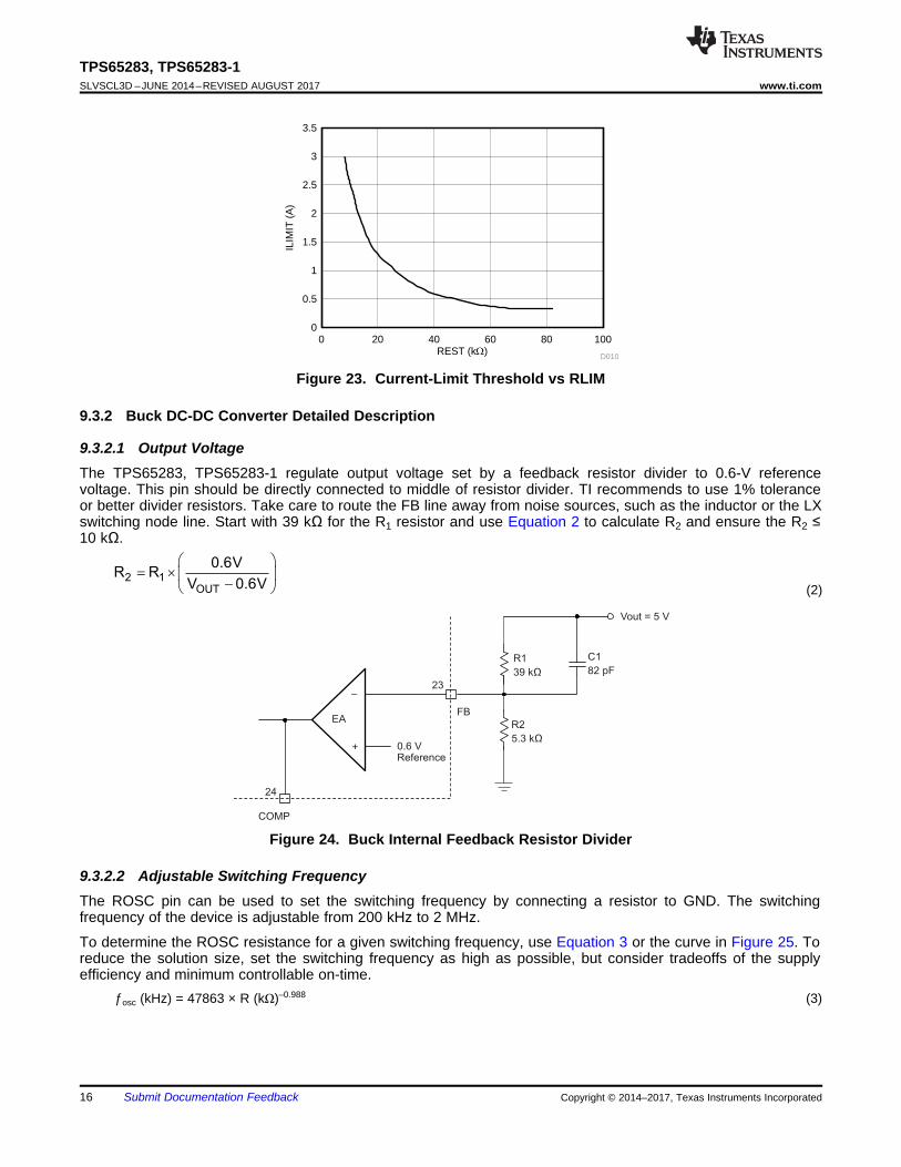
9.3.1.7 Programming the Current-Limit ThresholdThe overcurrent threshold is user programmable through an external resistor. The TPS65283, TPS65283-1 usesan internal regulation loop to provide a regulated voltage on the RLIM pin. The current-limit threshold isproportional to the current sourced out of RSET. The recommended 1% resistor range for RSET is 9.1 kΩ ≤RLIM ≤ 80.6 kΩ to adjust the current limit of the switch. Many applications require that the minimum current limitis above a certain current level or that the maximum current limit is below a certain current level, so it isimportant to consider the tolerance of the overcurrent threshold when selecting a value for RLIM. The followingequations and Figure 23 can be used to calculate the resulting overcurrent threshold for a given external resistorvalue (RSET).
Current-Limit Threshold Equations (IOS):ILIMIT = 37.793(RSET)–1.149 (1)
FB
R1
39 kΩ
R2
5.3 kΩ
C1
82 pF
23
COMP
24
–
+
EA
0.6 VReference
Vout = 5 V
2 1
OUT
0.6VR R
V 0.6V
æ ö= ´ ç ÷
-è ø
REST (k:)
ILIM
IT (
A)
0 20 40 60 80 1000
0.5
1
1.5
2
2.5
3
3.5
D010
16
TPS65283, TPS65283-1SLVSCL3D –JUNE 2014–REVISED AUGUST 2017 www.ti.com
Submit Documentation Feedback Copyright © 2014–2017, Texas Instruments Incorporated
Figure 23. Current-Limit Threshold vs RLIM
9.3.2 Buck DC-DC Converter Detailed Description
9.3.2.1 Output VoltageThe TPS65283, TPS65283-1 regulate output voltage set by a feedback resistor divider to 0.6-V referencevoltage. This pin should be directly connected to middle of resistor divider. TI recommends to use 1% toleranceor better divider resistors. Take care to route the FB line away from noise sources, such as the inductor or the LXswitching node line. Start with 39 kΩ for the R1 resistor and use Equation 2 to calculate R2 and ensure the R2 ≤10 kΩ.
(2)
Figure 24. Buck Internal Feedback Resistor Divider
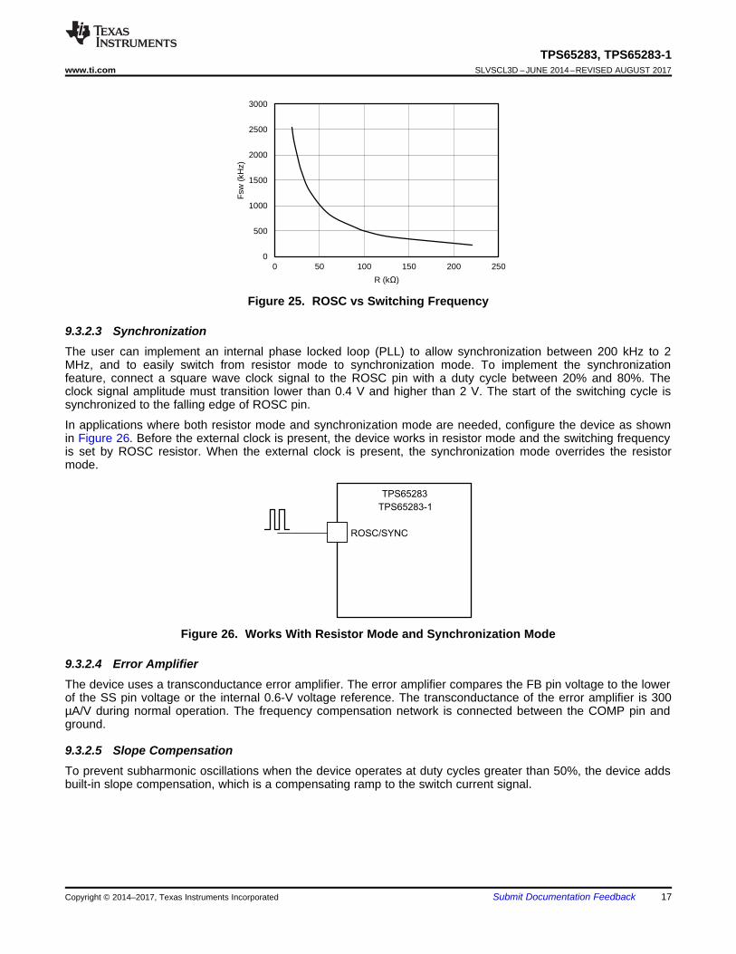
9.3.2.2 Adjustable Switching FrequencyThe ROSC pin can be used to set the switching frequency by connecting a resistor to GND. The switchingfrequency of the device is adjustable from 200 kHz to 2 MHz.
To determine the ROSC resistance for a given switching frequency, use Equation 3 or the curve in Figure 25. Toreduce the solution size, set the switching frequency as high as possible, but consider tradeoffs of the supplyefficiency and minimum controllable on-time.
ƒosc (kHz) = 47863 × R (kΩ)–0.988 (3)
ROSC/SYNC
TPS65283
TPS65283-1
0
500
1000
1500
2000
2500
3000
0 50 100 150 200 250
Fsw
(kH
z)
R (k) C011
17
TPS65283, TPS65283-1www.ti.com SLVSCL3D –JUNE 2014–REVISED AUGUST 2017
Submit Documentation FeedbackCopyright © 2014–2017, Texas Instruments Incorporated
Figure 25. ROSC vs Switching Frequency
9.3.2.3 SynchronizationThe user can implement an internal phase locked loop (PLL) to allow synchronization between 200 kHz to 2MHz, and to easily switch from resistor mode to synchronization mode. To implement the synchronizationfeature, connect a square wave clock signal to the ROSC pin with a duty cycle between 20% and 80%. Theclock signal amplitude must transition lower than 0.4 V and higher than 2 V. The start of the switching cycle issynchronized to the falling edge of ROSC pin.
In applications where both resistor mode and synchronization mode are needed, configure the device as shownin Figure 26. Before the external clock is present, the device works in resistor mode and the switching frequencyis set by ROSC resistor. When the external clock is present, the synchronization mode overrides the resistormode.
Figure 26. Works With Resistor Mode and Synchronization Mode
9.3.2.4 Error AmplifierThe device uses a transconductance error amplifier. The error amplifier compares the FB pin voltage to the lowerof the SS pin voltage or the internal 0.6-V voltage reference. The transconductance of the error amplifier is 300µA/V during normal operation. The frequency compensation network is connected between the COMP pin andground.
9.3.2.5 Slope CompensationTo prevent subharmonic oscillations when the device operates at duty cycles greater than 50%, the device addsbuilt-in slope compensation, which is a compensating ramp to the switch current signal.
( )1 ENFALLING
2
STOP ENFALLING 1 h p
R VR
V V R I I
´=
- + +
ENFALLINGSTART STOP
ENRISING
1
ENFALLINGP h
ENRISING
VV V
VR
VI 1 I
V
æ ö-ç ÷
è ø=æ ö
- +ç ÷è ø
9
Enable Threshold
TPS65283
TPS65283-1
VIN
EN
R1
R2
Ip Ih
Copyright © 2016, Texas Instruments Incorporated
18
TPS65283, TPS65283-1SLVSCL3D –JUNE 2014–REVISED AUGUST 2017 www.ti.com
Submit Documentation Feedback Copyright © 2014–2017, Texas Instruments Incorporated
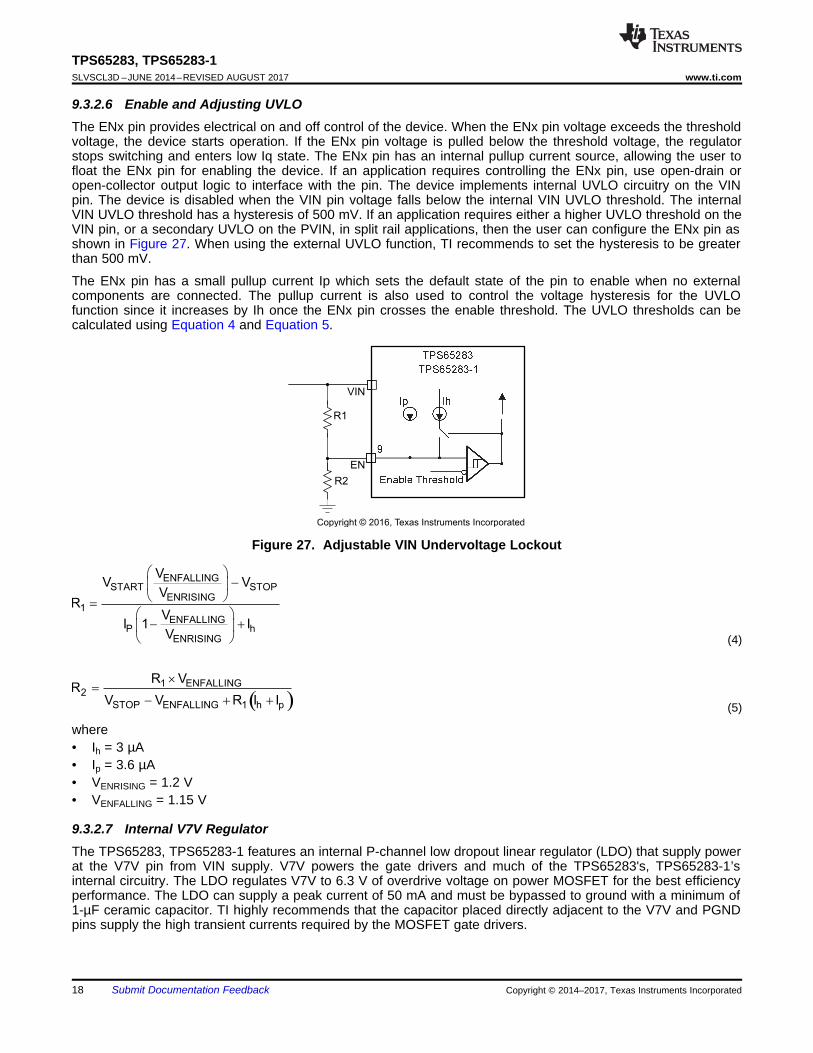
9.3.2.6 Enable and Adjusting UVLOThe ENx pin provides electrical on and off control of the device. When the ENx pin voltage exceeds the thresholdvoltage, the device starts operation. If the ENx pin voltage is pulled below the threshold voltage, the regulatorstops switching and enters low Iq state. The ENx pin has an internal pullup current source, allowing the user tofloat the ENx pin for enabling the device. If an application requires controlling the ENx pin, use open-drain oropen-collector output logic to interface with the pin. The device implements internal UVLO circuitry on the VINpin. The device is disabled when the VIN pin voltage falls below the internal VIN UVLO threshold. The internalVIN UVLO threshold has a hysteresis of 500 mV. If an application requires either a higher UVLO threshold on theVIN pin, or a secondary UVLO on the PVIN, in split rail applications, then the user can configure the ENx pin asshown in Figure 27. When using the external UVLO function, TI recommends to set the hysteresis to be greaterthan 500 mV.
The ENx pin has a small pullup current Ip which sets the default state of the pin to enable when no externalcomponents are connected. The pullup current is also used to control the voltage hysteresis for the UVLOfunction since it increases by Ih once the ENx pin crosses the enable threshold. The UVLO thresholds can becalculated using Equation 4 and Equation 5.
Figure 27. Adjustable VIN Undervoltage Lockout
(4)
spacer
(5)
where• Ih = 3 µA• Ip = 3.6 µA• VENRISING = 1.2 V• VENFALLING = 1.15 V
9.3.2.7 Internal V7V RegulatorThe TPS65283, TPS65283-1 features an internal P-channel low dropout linear regulator (LDO) that supply powerat the V7V pin from VIN supply. V7V powers the gate drivers and much of the TPS65283's, TPS65283-1’sinternal circuitry. The LDO regulates V7V to 6.3 V of overdrive voltage on power MOSFET for the best efficiencyperformance. The LDO can supply a peak current of 50 mA and must be bypassed to ground with a minimum of1-µF ceramic capacitor. TI highly recommends that the capacitor placed directly adjacent to the V7V and PGNDpins supply the high transient currents required by the MOSFET gate drivers.
4 ms
64 ms
Vout
IL
VLX
Current limit threshold
19
TPS65283, TPS65283-1www.ti.com SLVSCL3D –JUNE 2014–REVISED AUGUST 2017
Submit Documentation FeedbackCopyright © 2014–2017, Texas Instruments Incorporated
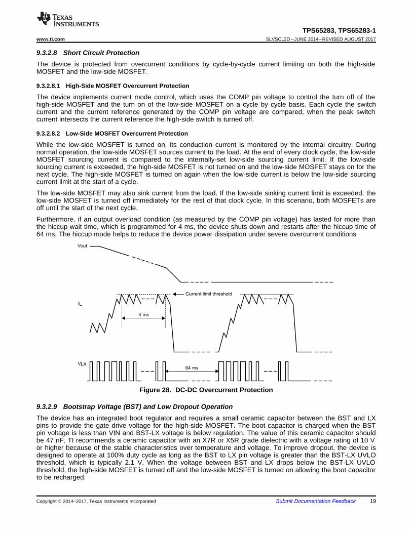
9.3.2.8 Short Circuit ProtectionThe device is protected from overcurrent conditions by cycle-by-cycle current limiting on both the high-sideMOSFET and the low-side MOSFET.
9.3.2.8.1 High-Side MOSFET Overcurrent Protection
The device implements current mode control, which uses the COMP pin voltage to control the turn off of thehigh-side MOSFET and the turn on of the low-side MOSFET on a cycle by cycle basis. Each cycle the switchcurrent and the current reference generated by the COMP pin voltage are compared, when the peak switchcurrent intersects the current reference the high-side switch is turned off.
9.3.2.8.2 Low-Side MOSFET Overcurrent Protection
While the low-side MOSFET is turned on, its conduction current is monitored by the internal circuitry. Duringnormal operation, the low-side MOSFET sources current to the load. At the end of every clock cycle, the low-sideMOSFET sourcing current is compared to the internally-set low-side sourcing current limit. If the low-sidesourcing current is exceeded, the high-side MOSFET is not turned on and the low-side MOSFET stays on for thenext cycle. The high-side MOSFET is turned on again when the low-side current is below the low-side sourcingcurrent limit at the start of a cycle.
The low-side MOSFET may also sink current from the load. If the low-side sinking current limit is exceeded, thelow-side MOSFET is turned off immediately for the rest of that clock cycle. In this scenario, both MOSFETs areoff until the start of the next cycle.
Furthermore, if an output overload condition (as measured by the COMP pin voltage) has lasted for more thanthe hiccup wait time, which is programmed for 4 ms, the device shuts down and restarts after the hiccup time of64 ms. The hiccup mode helps to reduce the device power dissipation under severe overcurrent conditions
Figure 28. DC-DC Overcurrent Protection
9.3.2.9 Bootstrap Voltage (BST) and Low Dropout OperationThe device has an integrated boot regulator and requires a small ceramic capacitor between the BST and LXpins to provide the gate drive voltage for the high-side MOSFET. The boot capacitor is charged when the BSTpin voltage is less than VIN and BST-LX voltage is below regulation. The value of this ceramic capacitor shouldbe 47 nF. TI recommends a ceramic capacitor with an X7R or X5R grade dielectric with a voltage rating of 10 Vor higher because of the stable characteristics over temperature and voltage. To improve dropout, the device isdesigned to operate at 100% duty cycle as long as the BST to LX pin voltage is greater than the BST-LX UVLOthreshold, which is typically 2.1 V. When the voltage between BST and LX drops below the BST-LX UVLOthreshold, the high-side MOSFET is turned off and the low-side MOSFET is turned on allowing the boot capacitorto be recharged.
EN Threshold
PGOODx
VIN
PGOOD Deglitch Time
T = C × 0.6 V / 5 µASS
T = C × (1.2 – 0.4) V / 3.6 µAENX
T = C × 0.4 V / 1.4 uAENX
Pre-Bias Startup
EN ThresholdEnx Rise TimeDictated by CEN
Charge C
with 6.6 µAEN
ENx
BUCKx
V7V
Soft Start Rise TimeDictated by CSS
20
TPS65283, TPS65283-1SLVSCL3D –JUNE 2014–REVISED AUGUST 2017 www.ti.com
Submit Documentation Feedback Copyright © 2014–2017, Texas Instruments Incorporated
9.3.2.10 Output Overvoltage Protection (OVP)The device incorporates an output OVP circuit to minimize output voltage overshoot. For example, when thepower supply output is overloaded, the error amplifier compares the actual output voltage to the internalreference voltage. If the FB pin voltage is lower than the internal reference voltage for a considerable time, theoutput of the error amplifier demands maximum output current. After the condition is removed, the regulatoroutput rises and the error amplifier output transitions to the steady state voltage. In some applications with smalloutput capacitance, the power supply output voltage can respond faster than the error amplifier. This leads to thepossibility of an output overshoot. The OVP feature minimizes the overshoot by comparing the FB pin voltage tothe OVP threshold. If the FB pin voltage is greater than the OVP threshold, the high-side MOSFET is turned off,preventing current from flowing to the output and minimizing output overshoot. When the FB voltage drops lowerthan the OVP threshold, the high-side MOSFET is allowed to turn on at the next clock cycle.
9.3.2.11 Power GoodThe PGOOD pin is an open-drain output. The PGOOD pin is pulled low when buck converter is pulled below92.5% or over 107.5% of the nominal output voltage. The PGOOD is pulled up when the buck converters’outputs are more than 95% and lower than 105% of its nominal output voltage. The default reset time is 2 ms.The polarity of the PGOOD is active high.
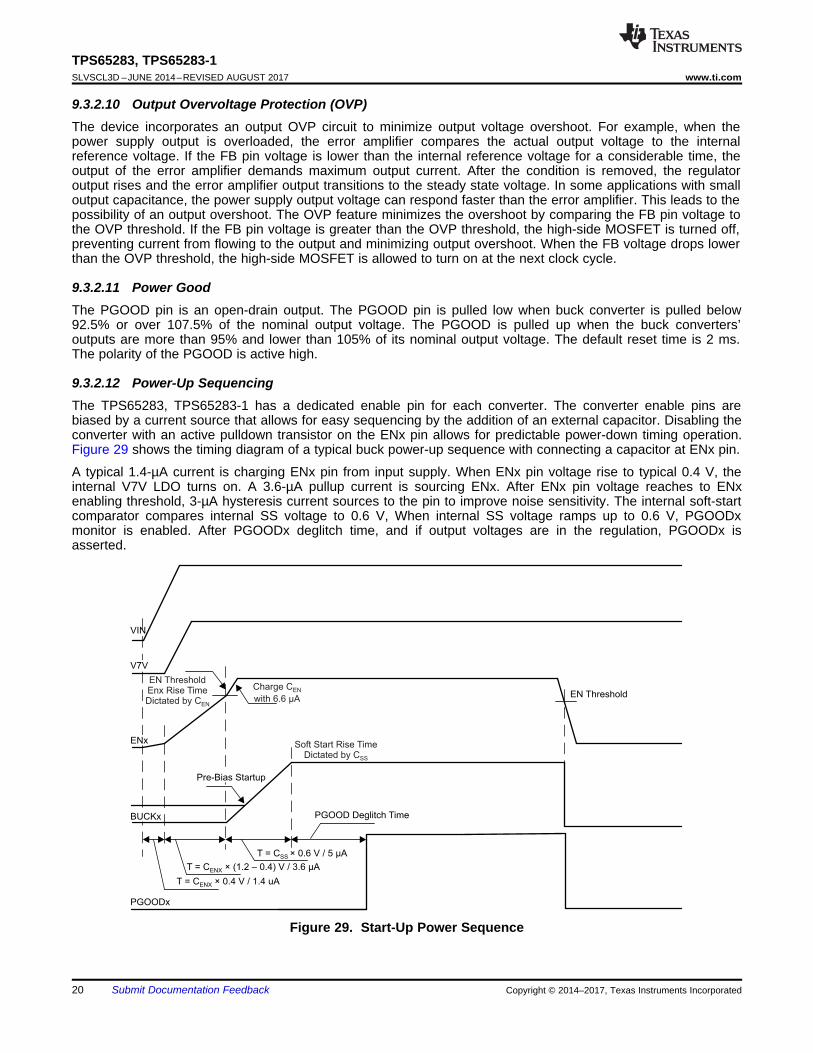
9.3.2.12 Power-Up SequencingThe TPS65283, TPS65283-1 has a dedicated enable pin for each converter. The converter enable pins arebiased by a current source that allows for easy sequencing by the addition of an external capacitor. Disabling theconverter with an active pulldown transistor on the ENx pin allows for predictable power-down timing operation.Figure 29 shows the timing diagram of a typical buck power-up sequence with connecting a capacitor at ENx pin.
A typical 1.4-µA current is charging ENx pin from input supply. When ENx pin voltage rise to typical 0.4 V, theinternal V7V LDO turns on. A 3.6-µA pullup current is sourcing ENx. After ENx pin voltage reaches to ENxenabling threshold, 3-µA hysteresis current sources to the pin to improve noise sensitivity. The internal soft-startcomparator compares internal SS voltage to 0.6 V, When internal SS voltage ramps up to 0.6 V, PGOODxmonitor is enabled. After PGOODx deglitch time, and if output voltages are in the regulation, PGOODx isasserted.
Figure 29. Start-Up Power Sequence
21
TPS65283, TPS65283-1www.ti.com SLVSCL3D –JUNE 2014–REVISED AUGUST 2017
Submit Documentation FeedbackCopyright © 2014–2017, Texas Instruments Incorporated
9.3.2.13 Thermal PerformanceThe device implements an internal thermal shutdown to protect itself if the junction temperature exceeds 160°C.The thermal shutdown forces the buck converter to stop switching when the junction temperature exceedsthermal trip threshold. After the die temperature decreases below 140°C, the device reinitiates the power-upsequence. The thermal shutdown hysteresis is 20°C. When USB is over-current, the internal thermal shut downof power switch will be changed to 145°C to avoid influencing the normal operation of buck converters.
9.4 Device Functional Modes
9.4.1 Operation With VIN < 4.5 V (Minimum VIN)The devices operate with input voltages above 4.5 V. The maximum UVLO voltage is 4.5 V and operates at inputvoltages above 4.5 V. The typical UVLO voltage is 4 V, and the devices may operate at input voltages above thatpoint. The devices also may operate at lower input voltage; the minimum UVLO voltage is not specified. At inputvoltages below the actual UVLO voltage, the devices do not operate.
9.4.2 Operation With EN ControlThe enable rising edge threshold voltage is 1.2 V typical and 1.26 V maximum. With EN held below that voltagethe device is disabled and switching is inhibited. The IC quiescent current is reduced in this state. When inputvoltage is above the UVLO threshold and the EN voltage is increased above the rising edge threshold, thedevice becomes active. Switching is enabled, and the slow start sequence is initiated. The TPS65283,TPS65283-1 output voltage ramps up at the internal slow-start time of 2.4 ms.
9.4.3 Operation at Light LoadsThe devices are designed to operate in high-efficiency PSM under light load conditions. Pulse skipping is initiatedwhen the switch current falls to 0 A. During pulse skipping, the low-side FET is turned off when the switch currentfalls to 0 A. The switching node (LX) waveform takes on the characteristics of DCM operation and the apparentswitching frequency decreases.
TPS65283
BST2
LX2
PGND2
VIN2
SW_IN
SW_OUT
FB
2
CO
MP
2
RS
ET
AG
ND
CO
MP
1
FB
1
BST1
LX1
PGND1
VIN1
V7V
PGOOD1
nFA
ULT
SW
_EN
EN
2
EN
1
RO
SC
/SY
NC
PG
OO
D2
VIN 5.5V~18V
USB Data
PGOOD2
USB fault signal
R24100k
C1947pF
C2210uF
R2100K
R1100k
19
20
21
22
23
24
4321 65
151618 17 131412
11
10
9
8
7
Ena
ble
pow
er s
witc
hL1
4.7uH
Analog Ground Power Ground
V7V
Vout1
1.2V/3.5AVout2
5V/2.5A
VIN 5.5V~18V
L24.7uH
Ena
ble
BC
UK
2
Ena
ble
BC
UK
1
DVCC
R1810K
R1720K
C173.3nF
R1320K
R1520K
C133.3nF
R1910K
C2022uF*2 C11
22uF*2C1247nF
C1010uF
C710uF
R6100K
R145.49K
C1282pF
R1240.2K
C1947nF
C231uF
PGOOD1
USB Port
Copyright © 2017, Texas Instruments Incorporated
22
TPS65283, TPS65283-1SLVSCL3D –JUNE 2014–REVISED AUGUST 2017 www.ti.com
Submit Documentation Feedback Copyright © 2014–2017, Texas Instruments Incorporated
10 Application and Implementation
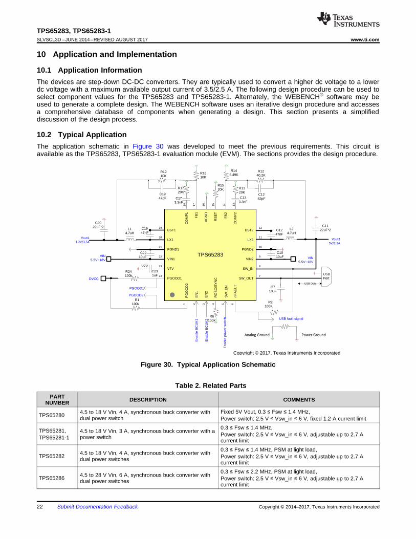
10.1 Application InformationThe devices are step-down DC-DC converters. They are typically used to convert a higher dc voltage to a lowerdc voltage with a maximum available output current of 3.5/2.5 A. The following design procedure can be used toselect component values for the TPS65283 and TPS65283-1. Alternately, the WEBENCH® software may beused to generate a complete design. The WEBENCH software uses an iterative design procedure and accessesa comprehensive database of components when generating a design. This section presents a simplifieddiscussion of the design process.
10.2 Typical ApplicationThe application schematic in Figure 30 was developed to meet the previous requirements. This circuit isavailable as the TPS65283, TPS65283-1 evaluation module (EVM). The sections provides the design procedure.
Figure 30. Typical Application Schematic
Table 2. Related PartsPART
NUMBER DESCRIPTION COMMENTS
TPS65280 4.5 to 18 V Vin, 4 A, synchronous buck converter withdual power switch
Fixed 5V Vout, 0.3 ≤ Fsw ≤ 1.4 MHz,Power switch: 2.5 V ≤ Vsw_in ≤ 6 V, fixed 1.2-A current limit
TPS65281,TPS65281-1
4.5 to 18 V Vin, 3 A, synchronous buck converter with apower switch
0.3 ≤ Fsw ≤ 1.4 MHz,Power switch: 2.5 V ≤ Vsw_in ≤ 6 V, adjustable up to 2.7 Acurrent limit
TPS65282 4.5 to 18 V Vin, 4 A, synchronous buck converter withdual power switches
0.3 ≤ Fsw ≤ 1.4 MHz, PSM at light load,Power switch: 2.5 V ≤ Vsw_in ≤ 6 V, adjustable up to 2.7 Acurrent limit
TPS65286 4.5 to 28 V Vin, 6 A, synchronous buck converter withdual power switches
0.3 ≤ Fsw ≤ 2.2 MHz, PSM at light load,Power switch: 2.5 V ≤ Vsw_in ≤ 6 V, adjustable up to 2.7 Acurrent limit
23
TPS65283, TPS65283-1www.ti.com SLVSCL3D –JUNE 2014–REVISED AUGUST 2017
Submit Documentation FeedbackCopyright © 2014–2017, Texas Instruments Incorporated
Typical Application (continued)Table 2. Related Parts (continued)
PARTNUMBER DESCRIPTION COMMENTS
TPS65287 4.5 to 18 V Vin, 3 A / 2 A / 2 A, triple synchronous buckconverter with a power switch and pushbutton control
0.3 ≤ Fsw ≤ 2.2 MHz, PSM at light load,Power switch: 2.5 V ≤ Vsw_in ≤ 6 V, adjustable up to 2.7 Acurrent limit
TPS65288 4.5 to 18 V Vin, 3 A / 2 A / 2 A, triple synchronous buckconverter with dual power switch
0.3 ≤ Fsw ≤ 2.2 MHz, PSM at light load,Power switch: 2.5 V ≤ Vsw_in ≤ 6 V, Fixed 1.2 A current limit
10.2.1 Design RequirementsFor this design example, use the following as the input parameters.
Table 3. Input ParametersPARAMETER EXAMPLE VALUE
Input voltage range 4.5 to 18 VOutput voltage 1.2 / 5 VTransient response, 1.5-A load step ΔVout = ±5%Input ripple voltage 400 mVOutput ripple voltage 30 mVOutput current rating 3.5 / 2.5 AOperating frequency 500 kHz
10.2.2 Detailed Design Procedure
10.2.2.1 Output Voltage SettingTo improve efficiency at light loads, consider using larger value resistors. If the values are too high, the regulatoris more sensitive to noise. Table 4 shows the recommended resistor values. Ensure the R2 ≤ 10 kΩ.
Table 4. Output Resistor Divider SelectionOUTPUT VOLTAGE
(V)R1
(kΩ)R2
(kΩ)1 6.8 10
1.2 10 101.5 15 101.8 20 102.5 31.6 103.3 45.3 103.3 22.6 4.995 73.2 105 36.5 4.99
2
OUT
out out
I LCo
V V
D ´>
´ D
LLpeak O
iI I
2
D= +
( ) 2
out inmax out
inmax2Lrms O
V V V
V L ƒswi I
12
æ ö´ -ç ÷ç ÷´ ´è ø= +
in out outL
in
V V Vi
L V ƒsw
-D = ´
´
in out out
O in
V V VL
I LIR ƒ
V sw
-
= ´
´ ´
24
TPS65283, TPS65283-1SLVSCL3D –JUNE 2014–REVISED AUGUST 2017 www.ti.com
Submit Documentation Feedback Copyright © 2014–2017, Texas Instruments Incorporated
10.2.2.2 Bootstrap Capacitor SelectionA 47-nF ceramic capacitor must be connected between the BST to LX pin for proper operation. TI recommendsto use a ceramic capacitor with X5R or better grade dielectric. The capacitor should have 10 V or higher voltagerating.
10.2.2.3 Inductor SelectionThe higher operating frequency allows the use of smaller inductor and capacitor values. A higher frequencygenerally results in lower efficiency because of MOSFET gate charge losses. In addition to this basic trade-off,consider the effect of inductor value on ripple current and low current operation. The ripple current depends onthe inductor value. The inductor ripple current iL decreases with higher inductance or higher frequency andincreases with higher input voltage VIN. Accepting larger values of iL allows the use of low inductances, butresults in higher output voltage ripple and greater core losses.
To calculate the value of the output inductor, use Equation 6. LIR is a coefficient that represents inductor peak-to-peak ripple to dc load current. LIR is suggested to choose to 0.1 to about 0.3 for most applications.
Actual core loss of inductor is independent of core size for a fixed inductor value, but it is very dependent oninductance value selected. As inductance increases, core losses go down. Unfortunately, increased inductancerequires more turns of wire and therefore copper losses increase. Ferrite designs have very-low core loss andare preferred for high switching frequencies, so design goals can concentrate on copper loss and preventingsaturation. Ferrite core material saturates hard, which means that inductance collapses abruptly when the peakdesign current is exceeded. It results in an abrupt increase in inductor ripple current and consequent outputvoltage ripple. Do not allow the core to saturate. It is important that the RMS current and saturation currentratings are not exceeding the inductor specification. Calculate the RMS and peak inductor current fromEquation 8 and Equation 9.
(6)
spacer
(7)
spacer
(8)
spacer
(9)
For this design example, use LIR = 0.3, and inductor is calculated to be 2.1 µH with Vin = 12 V, Vout = 1.2 V,Iout = 3.5 A. Choose 4.7-µH value of standard inductor, the peak-to-peak inductor ripple is about 13.1% of 3.5-Adc load current.
10.2.2.4 Output Capacitor SelectionThere are two primary considerations for selecting the value of the output capacitor. The output capacitors areselected to meet load transient and output ripple’s requirements. Equation 10 gives the minimum outputcapacitance to meet the transient specification. For this example, Lo = 4.7 µH, ΔIout = 2 A – 0.0 A = 2 A, andΔVout = 250 mV (5% of regulated 5 V) for Buck2. Using these numbers gives a minimum capacitance of 15 µF.This design uses a standard 2 × 22-µF ceramic.
(10)
outmaxin
in sw
I 0.25V
C ƒ
´D =
´
( )inmin outoutinrms out
inmin inmin
V VVI I
V V
-= ´ ´
SW
Vout (Vin max Vout)Icorms
12 Vin max L1 ƒ
´ -
=
´ ´ ´
VorippleResr
Ir leipp£
L
1 1Co
V8 ƒsw out esri
> ´D´
-D
25
TPS65283, TPS65283-1www.ti.com SLVSCL3D –JUNE 2014–REVISED AUGUST 2017
Submit Documentation FeedbackCopyright © 2014–2017, Texas Instruments Incorporated
The selection of COUT is driven by the effective series resistance (ESR). Equation 11 calculates the minimumoutput capacitance needed to meet the output voltage ripple specification. Where ƒsw is the switching frequency,ΔVout is the maximum allowable output voltage ripple, and ΔiL is the inductor ripple current. In this case, themaximum output voltage ripple is 25 mV (0.5% of regulated 5 V). From Equation 9, the output current ripple is1.24 A. From Equation 11, the minimum output capacitance meeting the output voltage ripple requirement is14.5 µF with 3-mΩ ESR resistance.
(11)
After considering both requirements, for this example, four 22-µF 6.3-V X7R ceramic capacitor with 3 mΩ of ESRare used. Equation 12 calculates the maximum ESR an output capacitor can have to meet the output voltageripple specification. Equation 12 indicates the ESR should be less than 20.2 mΩ. In this case, the ceramic caps’ESR is much smaller than 20.2 mΩ.
(12)
Factor in additional capacitance deratings for aging, temperature, and dc bias, which increase this minimumvalue. This example uses a 22-µF 6.3-V X5R ceramic capacitor with 3 mΩ of ESR. Capacitors generally havelimits to the amount of ripple current they can handle without failing or producing excess heat. An outputcapacitor that can support the inductor ripple current must be specified. Some capacitor data sheets specify theroot mean square (RMS) value of the maximum ripple current. Equation 13 can be used to calculate the RMSripple current the output capacitor needs to support. For this application, Equation 13 yields 385 mA.
(13)
10.2.2.5 Input Capacitor SelectionTI recommends a minimum 10-µF X7R/X5R ceramic input capacitor to be added between VIN and GND.Connect these capacitors as close as physically possible to the input pins of the converters as they handle theRMS ripple current shown in Equation 14. For this example, Iout = 2 A, Vout = 5 V, minimum Vin_min = 12 V,from Equation 14, the input capacitors must support a ripple current of 998-mA RMS.
(14)
The input capacitance value determines the input ripple voltage of the regulator. The input voltage ripple can becalculated using Equation 15. Using the design example values, Iout_max = 2.5 A, Cin = 10 µF, ƒSW = 500 kHzfor buck2, yields an input voltage ripple of 125 mV.
(15)
To prevent large voltage transients, use a low-ESR capacitor sized for the maximum RMS current.
10.2.2.6 Minimum Output VoltageDue to the internal design of the TPS65283, TPS65283-1, there is a minimum output voltage limit for any giveninput voltage. The output voltage can never be lower than the internal voltage reference of 0.6 V. Above 0.6 V,the output voltage may be limited by the minimum controllable on-time. The minimum output voltage in this caseis given by Equation 16.
Voutmin = Ontimemin × Fs max (Vin max + Iout min (RDS2 min – RDS1 min))_Iout min (RL + RDS2 min)
where• Voutmin = Minimum achievable output voltage• Ontimemin = Minimum controllable on-time (120-ns maximum)• Fsmax = Maximum switching frequency including tolerance• Vinmax = Maximum input voltage• Ioutmin = Minimum load current RDS1min = Minimum high-side MOSFET on-resistance (52-mΩ typical)
Current Sense
I/V Converter
ESRR
cR oC
cC
bC
LR
COMP
VfbEA
VOUT
VOUT
R
39 k1
ΩC1
R
5.3 k2
Ω
V = 0.6 Vref
g = 300 µSM g = 7.4 A/Vmps
iL
11 C
1C
5 ¦
S
ESRb
C
R CoC
R
LC
C
R CoC
R
pO L
1¦
C R 2
S
cC
M ps
¦ 9R &RR
g Vref gm
S
26
TPS65283, TPS65283-1SLVSCL3D –JUNE 2014–REVISED AUGUST 2017 www.ti.com
Submit Documentation Feedback Copyright © 2014–2017, Texas Instruments Incorporated
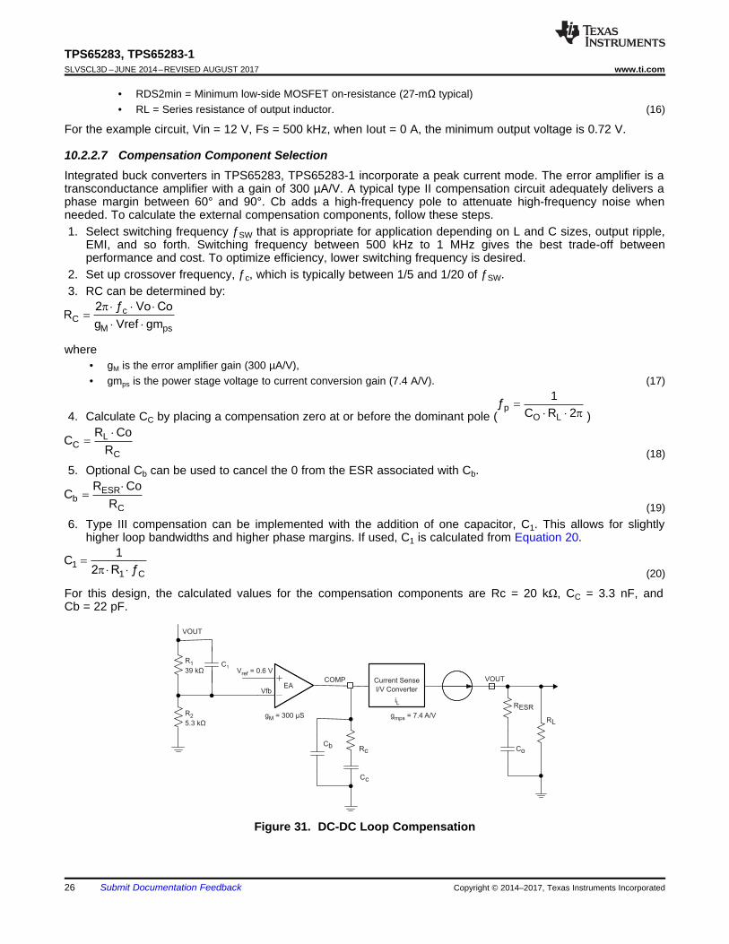
• RDS2min = Minimum low-side MOSFET on-resistance (27-mΩ typical)• RL = Series resistance of output inductor. (16)
For the example circuit, Vin = 12 V, Fs = 500 kHz, when Iout = 0 A, the minimum output voltage is 0.72 V.
10.2.2.7 Compensation Component SelectionIntegrated buck converters in TPS65283, TPS65283-1 incorporate a peak current mode. The error amplifier is atransconductance amplifier with a gain of 300 µA/V. A typical type II compensation circuit adequately delivers aphase margin between 60° and 90°. Cb adds a high-frequency pole to attenuate high-frequency noise whenneeded. To calculate the external compensation components, follow these steps.1. Select switching frequency ƒSW that is appropriate for application depending on L and C sizes, output ripple,
EMI, and so forth. Switching frequency between 500 kHz to 1 MHz gives the best trade-off betweenperformance and cost. To optimize efficiency, lower switching frequency is desired.
2. Set up crossover frequency, ƒc, which is typically between 1/5 and 1/20 of ƒSW.3. RC can be determined by:
where• gM is the error amplifier gain (300 µA/V),• gmps is the power stage voltage to current conversion gain (7.4 A/V). (17)
4. Calculate CC by placing a compensation zero at or before the dominant pole ( )
(18)5. Optional Cb can be used to cancel the 0 from the ESR associated with Cb.
(19)6. Type III compensation can be implemented with the addition of one capacitor, C1. This allows for slightly
higher loop bandwidths and higher phase margins. If used, C1 is calculated from Equation 20.
(20)
For this design, the calculated values for the compensation components are Rc = 20 kΩ, CC = 3.3 nF, andCb = 22 pF.
Figure 31. DC-DC Loop Compensation
27
TPS65283, TPS65283-1www.ti.com SLVSCL3D –JUNE 2014–REVISED AUGUST 2017
Submit Documentation FeedbackCopyright © 2014–2017, Texas Instruments Incorporated
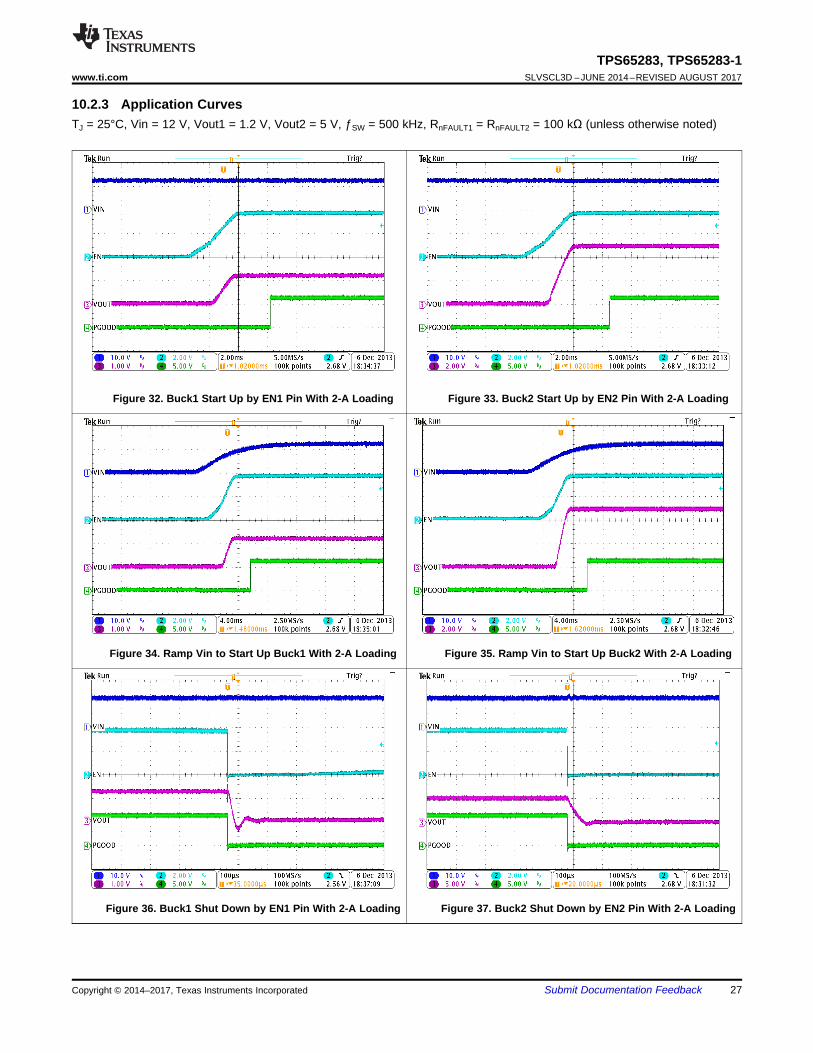
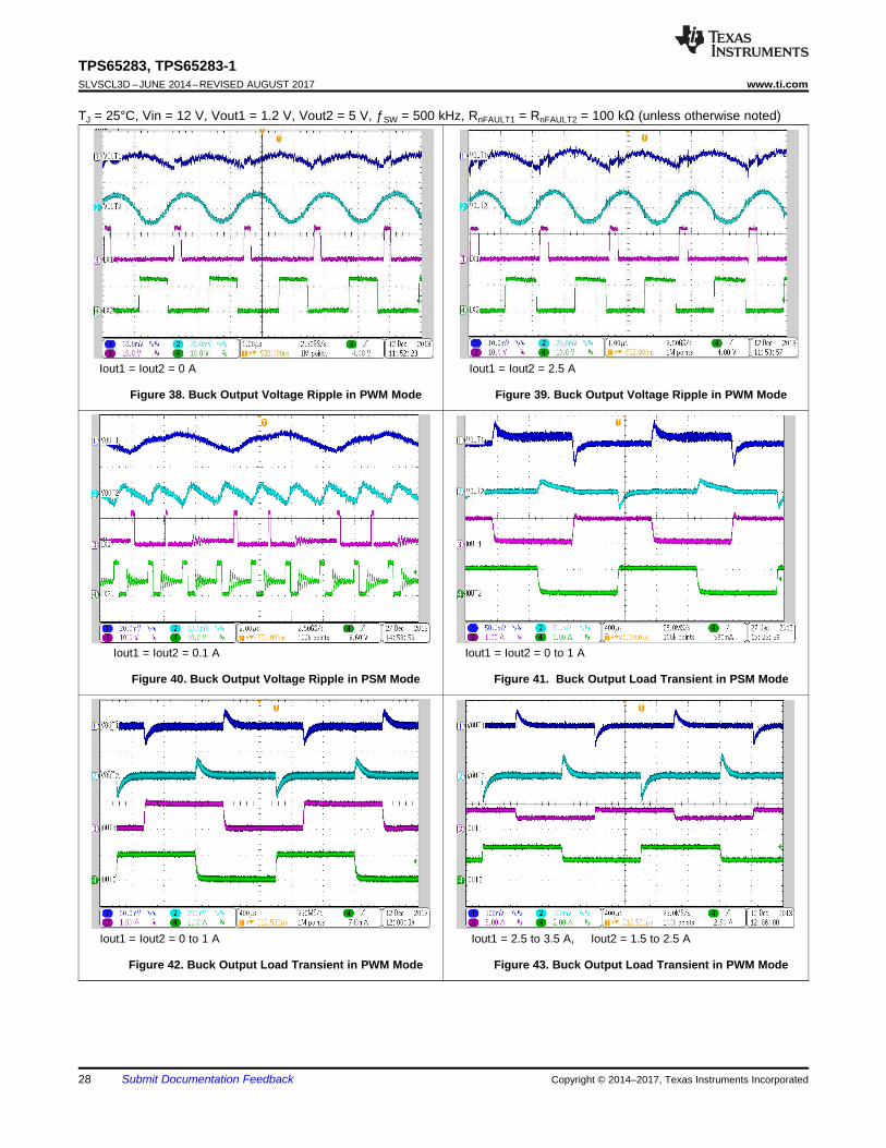
10.2.3 Application CurvesTJ = 25°C, Vin = 12 V, Vout1 = 1.2 V, Vout2 = 5 V, ƒSW = 500 kHz, RnFAULT1 = RnFAULT2 = 100 kΩ (unless otherwise noted)
Figure 32. Buck1 Start Up by EN1 Pin With 2-A Loading Figure 33. Buck2 Start Up by EN2 Pin With 2-A Loading
Figure 34. Ramp Vin to Start Up Buck1 With 2-A Loading Figure 35. Ramp Vin to Start Up Buck2 With 2-A Loading
Figure 36. Buck1 Shut Down by EN1 Pin With 2-A Loading Figure 37. Buck2 Shut Down by EN2 Pin With 2-A Loading
28
TPS65283, TPS65283-1SLVSCL3D –JUNE 2014–REVISED AUGUST 2017 www.ti.com
Submit Documentation Feedback Copyright © 2014–2017, Texas Instruments Incorporated
TJ = 25°C, Vin = 12 V, Vout1 = 1.2 V, Vout2 = 5 V, ƒSW = 500 kHz, RnFAULT1 = RnFAULT2 = 100 kΩ (unless otherwise noted)
Iout1 = Iout2 = 0 A
Figure 38. Buck Output Voltage Ripple in PWM Mode
Iout1 = Iout2 = 2.5 A
Figure 39. Buck Output Voltage Ripple in PWM Mode
Iout1 = Iout2 = 0.1 A
Figure 40. Buck Output Voltage Ripple in PSM Mode
Iout1 = Iout2 = 0 to 1 A
Figure 41. Buck Output Load Transient in PSM Mode
Iout1 = Iout2 = 0 to 1 A
Figure 42. Buck Output Load Transient in PWM Mode
Iout1 = 2.5 to 3.5 A, Iout2 = 1.5 to 2.5 A
Figure 43. Buck Output Load Transient in PWM Mode
29
TPS65283, TPS65283-1www.ti.com SLVSCL3D –JUNE 2014–REVISED AUGUST 2017
Submit Documentation FeedbackCopyright © 2014–2017, Texas Instruments Incorporated
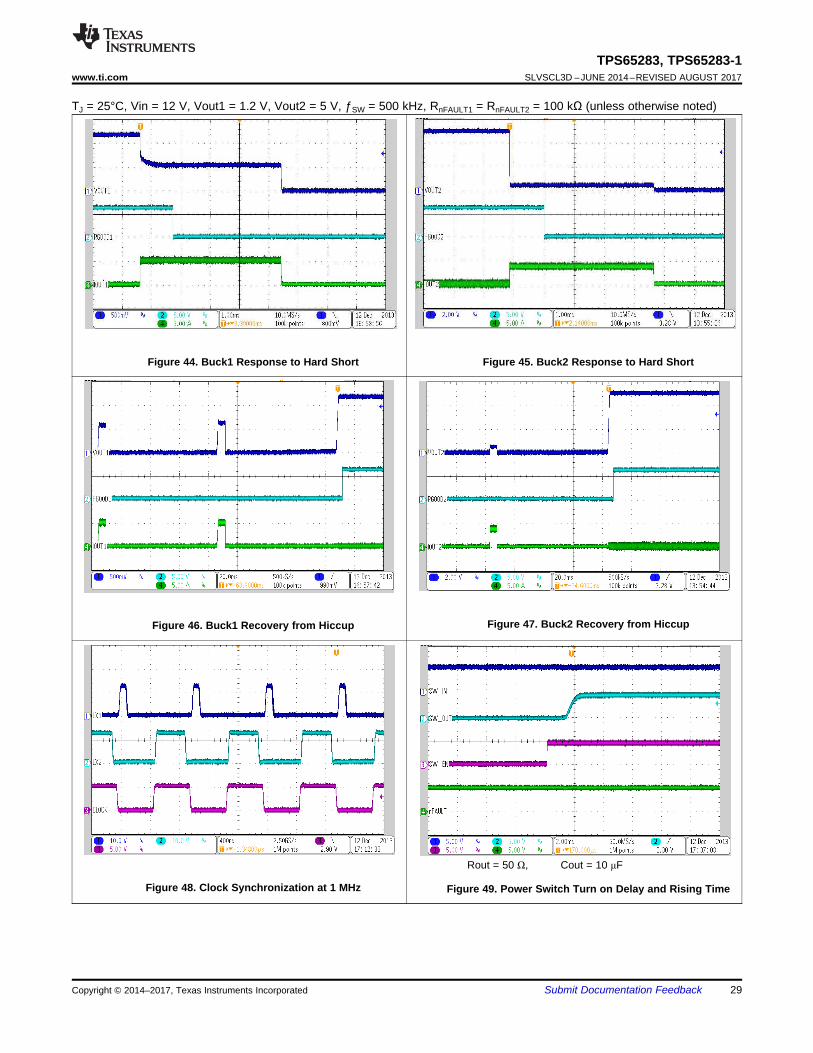
TJ = 25°C, Vin = 12 V, Vout1 = 1.2 V, Vout2 = 5 V, ƒSW = 500 kHz, RnFAULT1 = RnFAULT2 = 100 kΩ (unless otherwise noted)
Figure 44. Buck1 Response to Hard Short Figure 45. Buck2 Response to Hard Short
Figure 46. Buck1 Recovery from Hiccup Figure 47. Buck2 Recovery from Hiccup
Figure 48. Clock Synchronization at 1 MHz
Rout = 50 Ω, Cout = 10 μF
Figure 49. Power Switch Turn on Delay and Rising Time
30
TPS65283, TPS65283-1SLVSCL3D –JUNE 2014–REVISED AUGUST 2017 www.ti.com
Submit Documentation Feedback Copyright © 2014–2017, Texas Instruments Incorporated
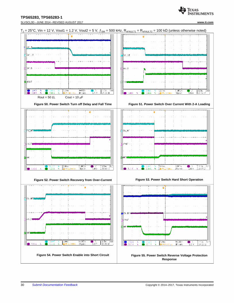
TJ = 25°C, Vin = 12 V, Vout1 = 1.2 V, Vout2 = 5 V, ƒSW = 500 kHz, RnFAULT1 = RnFAULT2 = 100 kΩ (unless otherwise noted)
Rout = 50 Ω, Cout = 10 μF
Figure 50. Power Switch Turn off Delay and Fall Time Figure 51. Power Switch Over Current With 2-A Loading
Figure 52. Power Switch Recovery from Over-Current Figure 53. Power Switch Hard Short Operation
Figure 54. Power Switch Enable into Short Circuit Figure 55. Power Switch Reverse Voltage ProtectionResponse
31
TPS65283, TPS65283-1www.ti.com SLVSCL3D –JUNE 2014–REVISED AUGUST 2017
Submit Documentation FeedbackCopyright © 2014–2017, Texas Instruments Incorporated
11 Power Supply RecommendationsThe devices are designed to operate from an input voltage supply range between 4.5 to 18 V. This input supplyshould be well regulated. If the input supply is located more than a few inches from the TPS65283 orTPS65283-1 converter, additional bulk capacitance may be required in addition to the ceramic bypass capacitors.A typical choice is an electrolytic capacitor with a value of 10 μF.
12 Layout
12.1 Layout Guidelines
12.1.1 PCB Layout RecommendationWhen laying out the PCB, use the following guidelines to ensure proper operation of the IC. These items are alsoshown in the layout diagram of Figure 58.• There are several signals paths that conduct fast changing currents or voltages that can interact with stray
inductance or parasitic capacitance to generate noise or degrade the power supply's performance. To helpeliminate these problems, the VIN pin should be bypassed to ground with a low-ESR ceramic bypasscapacitor with X5R or X7R dielectric. This capacitor provides the ac current into the internal power MOSFETs.Connect the (+) terminal of the input capacitor as close as possible to the VIN pin, and connect the (–)terminal of the input capacitor as close as possible to the PGND pin. Take care to minimize the loop areaformed by the bypass capacitor connections, the VIN pins, and the power ground PGND connections.
• Because the LX connection is the switching node, the output inductor should be located close to the LX pin,and the area of the PCB conductor minimized to prevent excessive capacitive coupling. Keep the switchingnode, LX, away from all sensitive small-signal nodes.
• Connect V7V decoupling capacitor connected close to the IC, between the V7V and the power ground PGNDpin. This capacitor carries the MOSFET drivers’ current peaks.
• Place the output filter capacitor of buck converter close to SW_IN pins. Try to minimize the ground conductorlength while maintaining adequate width.
• AGND pin should be separately routed to the (–) terminal of V7V bypass capacitor to avoid switchinggrounding path. TI recommends a ground plane connecting to this ground path.
• The compensation should be as close as possible to the COMP pins. The COMP and ROSC pins aresensitive to noise, so the components associated to these pins should be located as close as possible to theIC and routed with minimal lengths of trace. Flood all unused areas on all layers with copper. Flooding withcopper reduces the temperature rise of power components. You can connect the copper areas to PGND,AGND, VIN, or any other dc rail in the system.
• There is no electric signal internally connected to thermal pad in the device. Nevertheless, connect exposedpad beneath the IC to ground. Always solder thermal pad to the board and have as many vias as possible onthe PCB to enhance power dissipation.
12.1.2 Power Dissipation and Junction TemperatureThe total power dissipation inside TPS65283, TPS65283-1 should not to exceed the maximum allowable junctiontemperature of 125°C. The maximum allowable power dissipation is a function of the thermal resistance of thepackage (RθJA) and ambient temperature.
The following analysis gives an approximation in calculating junction temperature based on the power dissipationin the package. However, note that thermal analysis is strongly dependent on additional system-level factors.Such factors include air flow, board layout, copper thickness and surface area, and proximity to other devicesdissipating power. Good thermal design practice must include all system-level factors in addition to individualcomponent analysis.
To calculate the temperature inside the device under continuous load, use the following procedure.1. Define the total continuous current through buck converter (including the load current through power
switches). Make sure the continuous current does not exceed maximum load current requirement.2. From the graphs in this section, determine the expected losses (y-axis) in watts for buck converter inside the
device. The loss PD_BUCK depends on the input supply and the selected switching frequency.3. Determine the load current IOUT through the power switches. Read RDS(on) of power switch from the typical
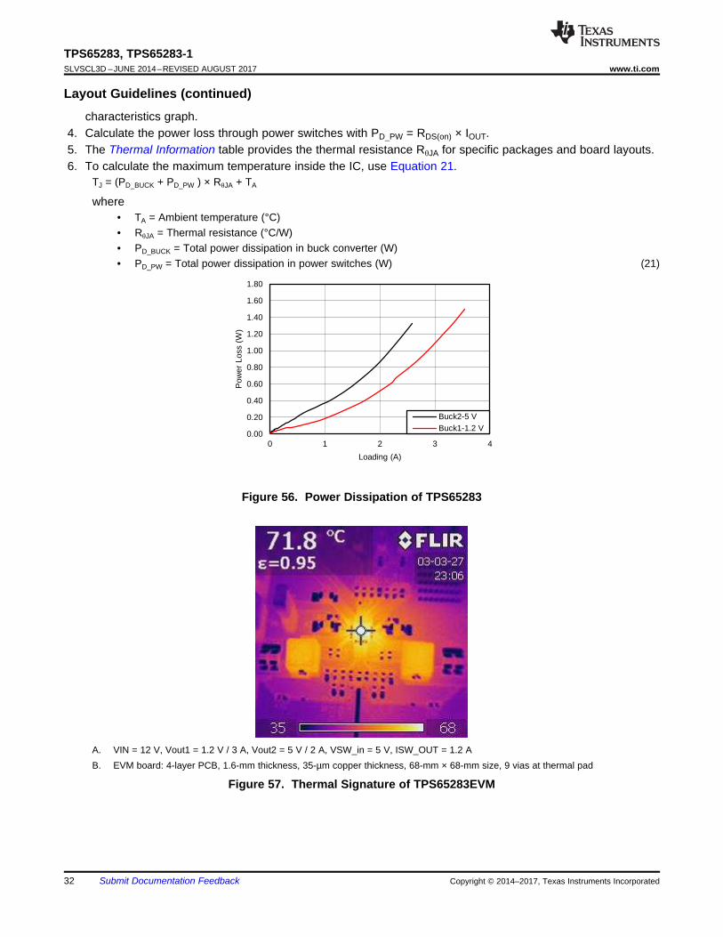
0.00
0.20
0.40
0.60
0.80
1.00
1.20
1.40
1.60
1.80
0 1 2 3 4
Pow
er L
oss
(W)
Loading (A)
Buck2-5 VBuck1-1.2 V
C012
32
TPS65283, TPS65283-1SLVSCL3D –JUNE 2014–REVISED AUGUST 2017 www.ti.com
Submit Documentation Feedback Copyright © 2014–2017, Texas Instruments Incorporated
Layout Guidelines (continued)characteristics graph.
4. Calculate the power loss through power switches with PD_PW = RDS(on) × IOUT.5. The Thermal Information table provides the thermal resistance RθJA for specific packages and board layouts.6. To calculate the maximum temperature inside the IC, use Equation 21.
TJ = (PD_BUCK + PD_PW ) × RθJA + TA
where• TA = Ambient temperature (°C)• RθJA = Thermal resistance (°C/W)• PD_BUCK = Total power dissipation in buck converter (W)• PD_PW = Total power dissipation in power switches (W) (21)
Figure 56. Power Dissipation of TPS65283
A. VIN = 12 V, Vout1 = 1.2 V / 3 A, Vout2 = 5 V / 2 A, VSW_in = 5 V, ISW_OUT = 1.2 AB. EVM board: 4-layer PCB, 1.6-mm thickness, 35-µm copper thickness, 68-mm × 68-mm size, 9 vias at thermal pad
Figure 57. Thermal Signature of TPS65283EVM
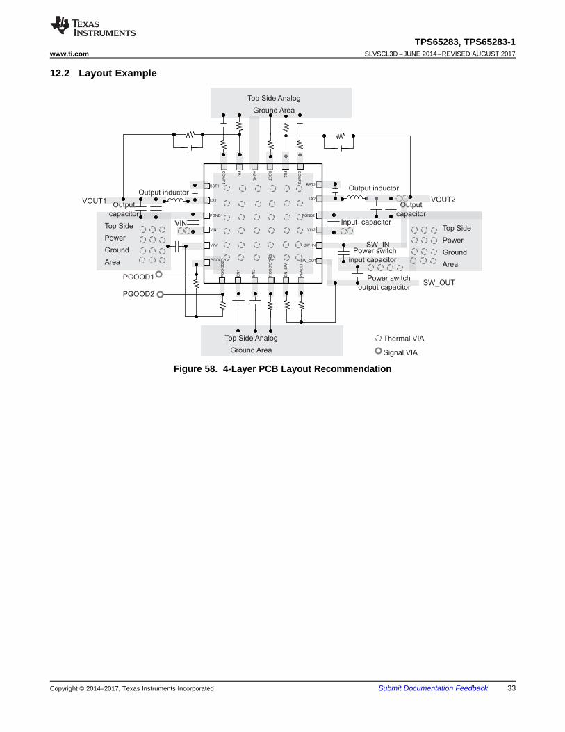
BST1
LX1
PGND1
PG
OO
D2
EN
1
EN
2
RO
SC
/SY
NC
VIN2
LX2
BST2
CO
MP
1
FB
1
AG
ND
RS
ET
Top Side Analog
Ground Area
SW_OUTPGOOD1
Output inductor
Input capacitor
Power switch
output capacitor
Thermal VIA
Signal VIA
VOUT2
VIN
V7V
PGND2
SW_IN
EN
_S
W
nFA
ULT
FB
2
CO
MP
2
VIN1
PGOOD1 SW_OUT
Top Side
Power
Ground
Area
Output
capacitor
Output inductor
Output
capacitor
PGOOD2
VOUT1
Power switch
input capacitor
Top Side
Power
Ground
Area
SW_IN
Top Side Analog
Ground Area
33
TPS65283, TPS65283-1www.ti.com SLVSCL3D –JUNE 2014–REVISED AUGUST 2017
Submit Documentation FeedbackCopyright © 2014–2017, Texas Instruments Incorporated
12.2 Layout Example
Figure 58. 4-Layer PCB Layout Recommendation
34
TPS65283, TPS65283-1SLVSCL3D –JUNE 2014–REVISED AUGUST 2017 www.ti.com
Submit Documentation Feedback Copyright © 2014–2017, Texas Instruments Incorporated
13 Device and Documentation Support
13.1 Documentation Support
13.1.1 Related LinksThe table below lists quick access links. Categories include technical documents, support and communityresources, tools and software, and quick access to sample or buy.
Table 5. Related Links
PARTS PRODUCT FOLDER SAMPLE & BUY TECHNICALDOCUMENTS
TOOLS &SOFTWARE
SUPPORT &COMMUNITY
TPS65283 Click here Click here Click here Click here Click hereTPS65283-1 Click here Click here Click here Click here Click here
13.2 TrademarksPowerPAD is a trademark of Texas Instruments.WEBENCH is a registered trademark of Texas Instruments.
13.3 Electrostatic Discharge CautionThese devices have limited built-in ESD protection. The leads should be shorted together or the device placed in conductive foamduring storage or handling to prevent electrostatic damage to the MOS gates.
13.4 GlossarySLYZ022 — TI Glossary.
This glossary lists and explains terms, acronyms, and definitions.
14 Mechanical, Packaging, and Orderable InformationThe following pages include mechanical, packaging, and orderable information. This information is the mostcurrent data available for the designated devices. This data is subject to change without notice and revision ofthis document. For browser-based versions of this data sheet, refer to the left-hand navigation.
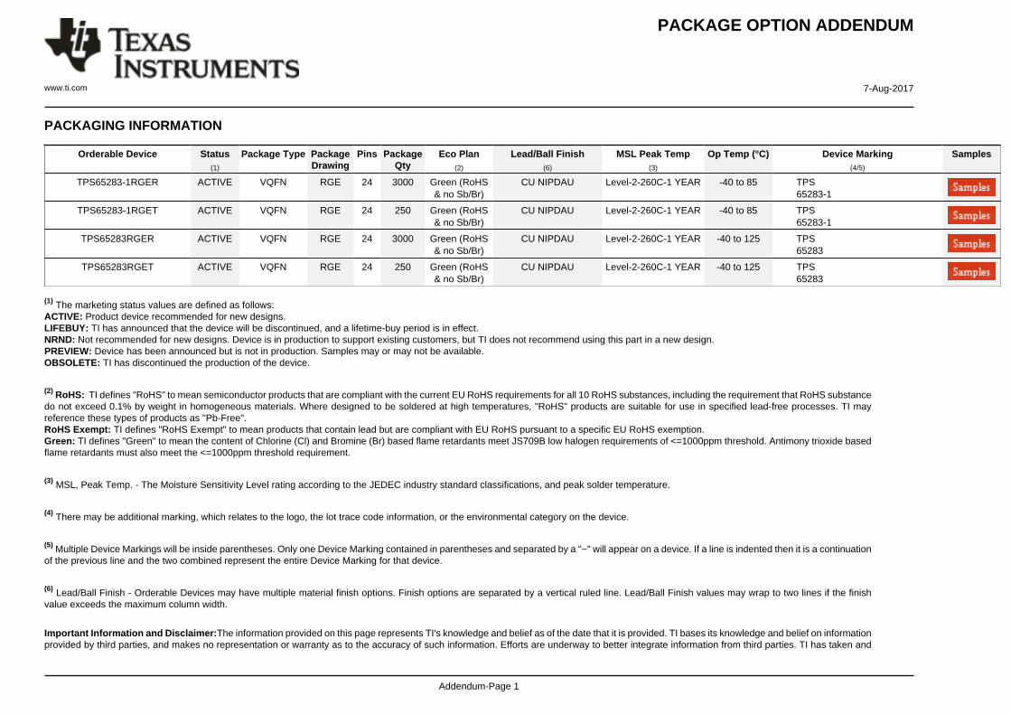
PACKAGE OPTION ADDENDUM
www.ti.com 7-Aug-2017
Addendum-Page 1
PACKAGING INFORMATION
Orderable Device Status(1)
Package Type PackageDrawing
Pins PackageQty
Eco Plan(2)
Lead/Ball Finish(6)
MSL Peak Temp(3)
Op Temp (°C) Device Marking(4/5)
Samples
TPS65283-1RGER ACTIVE VQFN RGE 24 3000 Green (RoHS& no Sb/Br)
CU NIPDAU Level-2-260C-1 YEAR -40 to 85 TPS65283-1
TPS65283-1RGET ACTIVE VQFN RGE 24 250 Green (RoHS& no Sb/Br)
CU NIPDAU Level-2-260C-1 YEAR -40 to 85 TPS65283-1
TPS65283RGER ACTIVE VQFN RGE 24 3000 Green (RoHS& no Sb/Br)
CU NIPDAU Level-2-260C-1 YEAR -40 to 125 TPS65283
TPS65283RGET ACTIVE VQFN RGE 24 250 Green (RoHS& no Sb/Br)
CU NIPDAU Level-2-260C-1 YEAR -40 to 125 TPS65283
(1) The marketing status values are defined as follows:ACTIVE: Product device recommended for new designs.LIFEBUY: TI has announced that the device will be discontinued, and a lifetime-buy period is in effect.NRND: Not recommended for new designs. Device is in production to support existing customers, but TI does not recommend using this part in a new design.PREVIEW: Device has been announced but is not in production. Samples may or may not be available.OBSOLETE: TI has discontinued the production of the device.
(2) RoHS: TI defines "RoHS" to mean semiconductor products that are compliant with the current EU RoHS requirements for all 10 RoHS substances, including the requirement that RoHS substancedo not exceed 0.1% by weight in homogeneous materials. Where designed to be soldered at high temperatures, "RoHS" products are suitable for use in specified lead-free processes. TI mayreference these types of products as "Pb-Free".RoHS Exempt: TI defines "RoHS Exempt" to mean products that contain lead but are compliant with EU RoHS pursuant to a specific EU RoHS exemption.Green: TI defines "Green" to mean the content of Chlorine (Cl) and Bromine (Br) based flame retardants meet JS709B low halogen requirements of <=1000ppm threshold. Antimony trioxide basedflame retardants must also meet the <=1000ppm threshold requirement.
(3) MSL, Peak Temp. - The Moisture Sensitivity Level rating according to the JEDEC industry standard classifications, and peak solder temperature.
(4) There may be additional marking, which relates to the logo, the lot trace code information, or the environmental category on the device.
(5) Multiple Device Markings will be inside parentheses. Only one Device Marking contained in parentheses and separated by a "~" will appear on a device. If a line is indented then it is a continuationof the previous line and the two combined represent the entire Device Marking for that device.
(6) Lead/Ball Finish - Orderable Devices may have multiple material finish options. Finish options are separated by a vertical ruled line. Lead/Ball Finish values may wrap to two lines if the finishvalue exceeds the maximum column width.
Important Information and Disclaimer:The information provided on this page represents TI's knowledge and belief as of the date that it is provided. TI bases its knowledge and belief on informationprovided by third parties, and makes no representation or warranty as to the accuracy of such information. Efforts are underway to better integrate information from third parties. TI has taken and

PACKAGE OPTION ADDENDUM
www.ti.com 7-Aug-2017
Addendum-Page 2
continues to take reasonable steps to provide representative and accurate information but may not have conducted destructive testing or chemical analysis on incoming materials and chemicals.TI and TI suppliers consider certain information to be proprietary, and thus CAS numbers and other limited information may not be available for release.
In no event shall TI's liability arising out of such information exceed the total purchase price of the TI part(s) at issue in this document sold by TI to Customer on an annual basis.
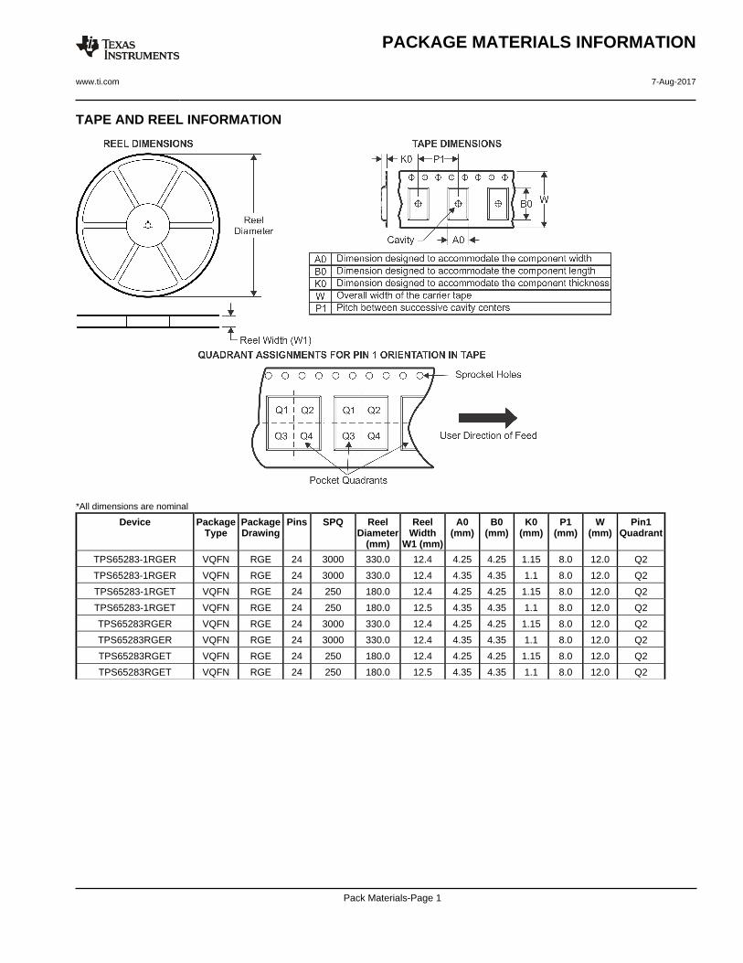
TAPE AND REEL INFORMATION
*All dimensions are nominal
Device PackageType
PackageDrawing
Pins SPQ ReelDiameter
(mm)
ReelWidth
W1 (mm)
A0(mm)
B0(mm)
K0(mm)
P1(mm)
W(mm)
Pin1Quadrant
TPS65283-1RGER VQFN RGE 24 3000 330.0 12.4 4.25 4.25 1.15 8.0 12.0 Q2
TPS65283-1RGER VQFN RGE 24 3000 330.0 12.4 4.35 4.35 1.1 8.0 12.0 Q2
TPS65283-1RGET VQFN RGE 24 250 180.0 12.4 4.25 4.25 1.15 8.0 12.0 Q2
TPS65283-1RGET VQFN RGE 24 250 180.0 12.5 4.35 4.35 1.1 8.0 12.0 Q2
TPS65283RGER VQFN RGE 24 3000 330.0 12.4 4.25 4.25 1.15 8.0 12.0 Q2
TPS65283RGER VQFN RGE 24 3000 330.0 12.4 4.35 4.35 1.1 8.0 12.0 Q2
TPS65283RGET VQFN RGE 24 250 180.0 12.4 4.25 4.25 1.15 8.0 12.0 Q2
TPS65283RGET VQFN RGE 24 250 180.0 12.5 4.35 4.35 1.1 8.0 12.0 Q2
PACKAGE MATERIALS INFORMATION
www.ti.com 7-Aug-2017
Pack Materials-Page 1
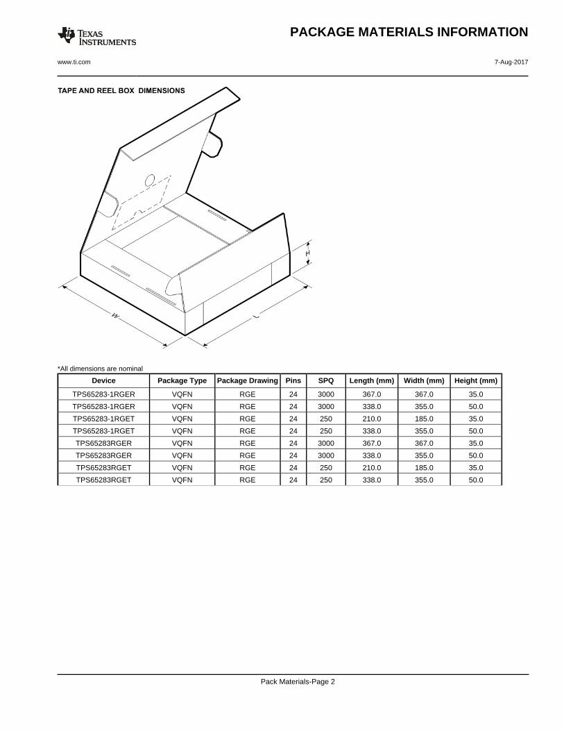
*All dimensions are nominal
Device Package Type Package Drawing Pins SPQ Length (mm) Width (mm) Height (mm)
TPS65283-1RGER VQFN RGE 24 3000 367.0 367.0 35.0
TPS65283-1RGER VQFN RGE 24 3000 338.0 355.0 50.0
TPS65283-1RGET VQFN RGE 24 250 210.0 185.0 35.0
TPS65283-1RGET VQFN RGE 24 250 338.0 355.0 50.0
TPS65283RGER VQFN RGE 24 3000 367.0 367.0 35.0
TPS65283RGER VQFN RGE 24 3000 338.0 355.0 50.0
TPS65283RGET VQFN RGE 24 250 210.0 185.0 35.0
TPS65283RGET VQFN RGE 24 250 338.0 355.0 50.0
PACKAGE MATERIALS INFORMATION
www.ti.com 7-Aug-2017
Pack Materials-Page 2
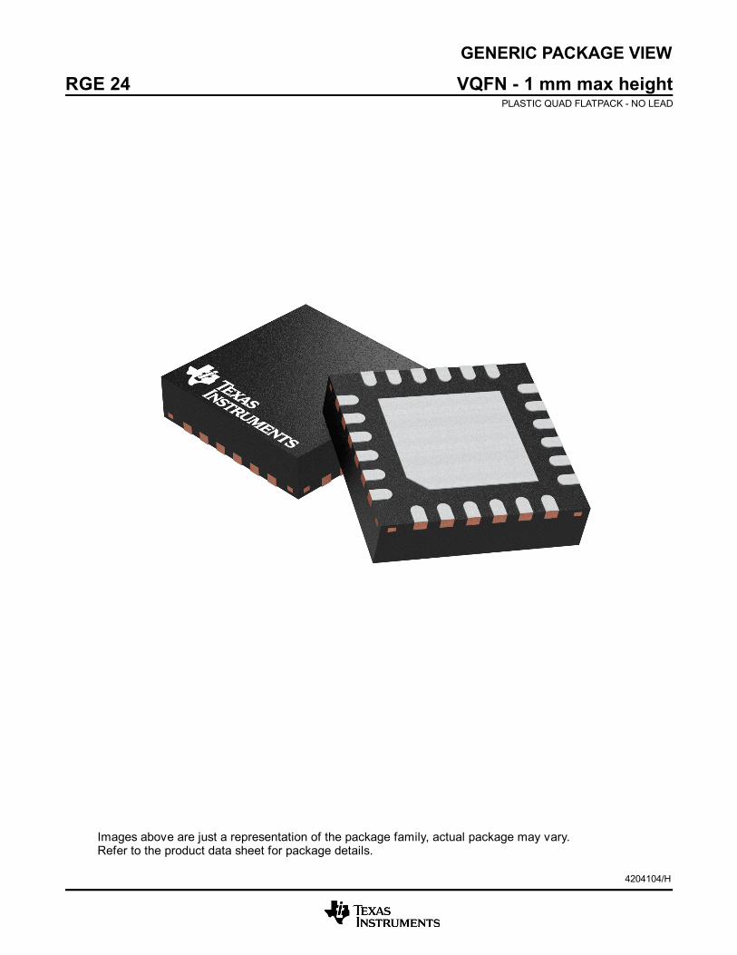
GENERIC PACKAGE VIEW
Images above are just a representation of the package family, actual package may vary.Refer to the product data sheet for package details.
RGE 24 VQFN - 1 mm max heightPLASTIC QUAD FLATPACK - NO LEAD
4204104/H
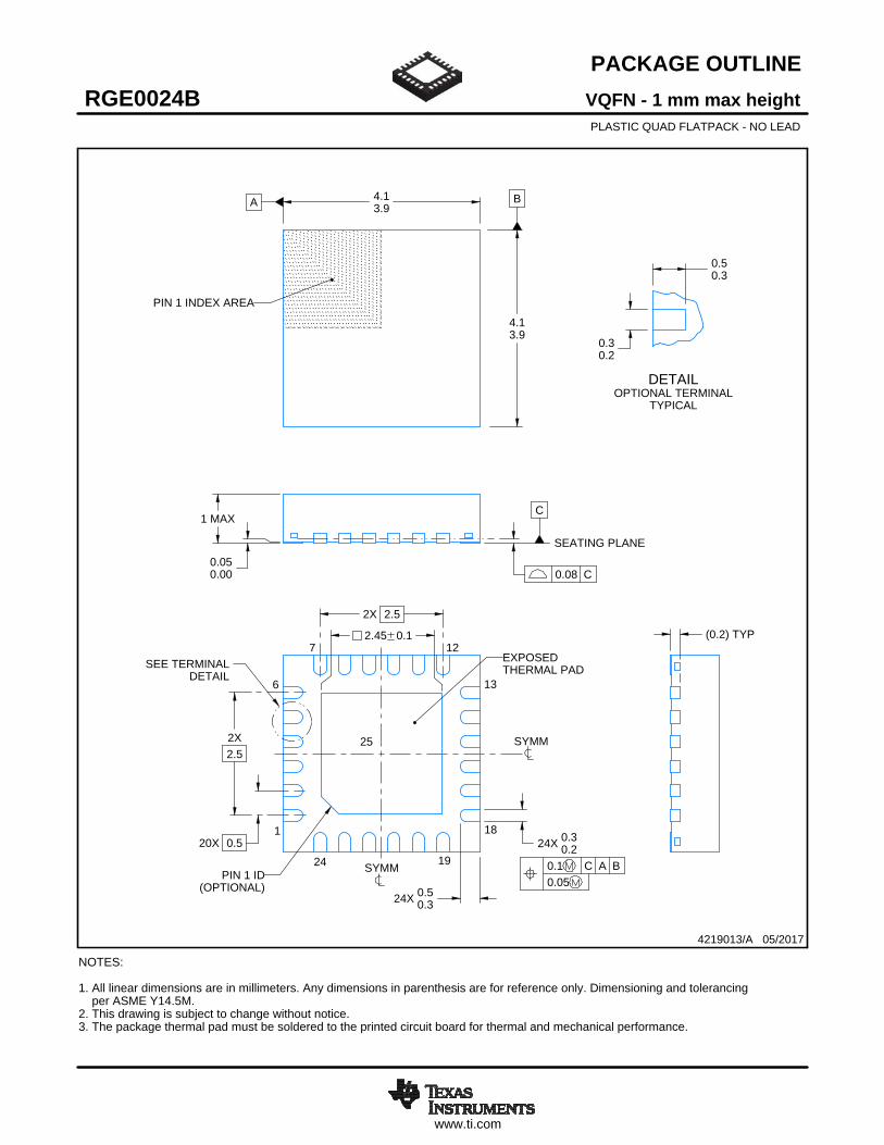
www.ti.com
PACKAGE OUTLINE
C
SEE TERMINALDETAIL
24X 0.30.2
2.45 0.1
24X 0.50.3
1 MAX
(0.2) TYP
0.050.00
20X 0.5
2X2.5
2X 2.5
A 4.13.9
B
4.13.9
0.30.2
0.50.3
VQFN - 1 mm max heightRGE0024BPLASTIC QUAD FLATPACK - NO LEAD
4219013/A 05/2017
PIN 1 INDEX AREA
0.08 C
SEATING PLANE
1
6 13
18
7 12
24 19
(OPTIONAL)PIN 1 ID
0.1 C A B0.05
EXPOSEDTHERMAL PAD
25 SYMM
SYMM
NOTES: 1. All linear dimensions are in millimeters. Any dimensions in parenthesis are for reference only. Dimensioning and tolerancing per ASME Y14.5M. 2. This drawing is subject to change without notice. 3. The package thermal pad must be soldered to the printed circuit board for thermal and mechanical performance.
SCALE 3.000
DETAILOPTIONAL TERMINAL
TYPICAL
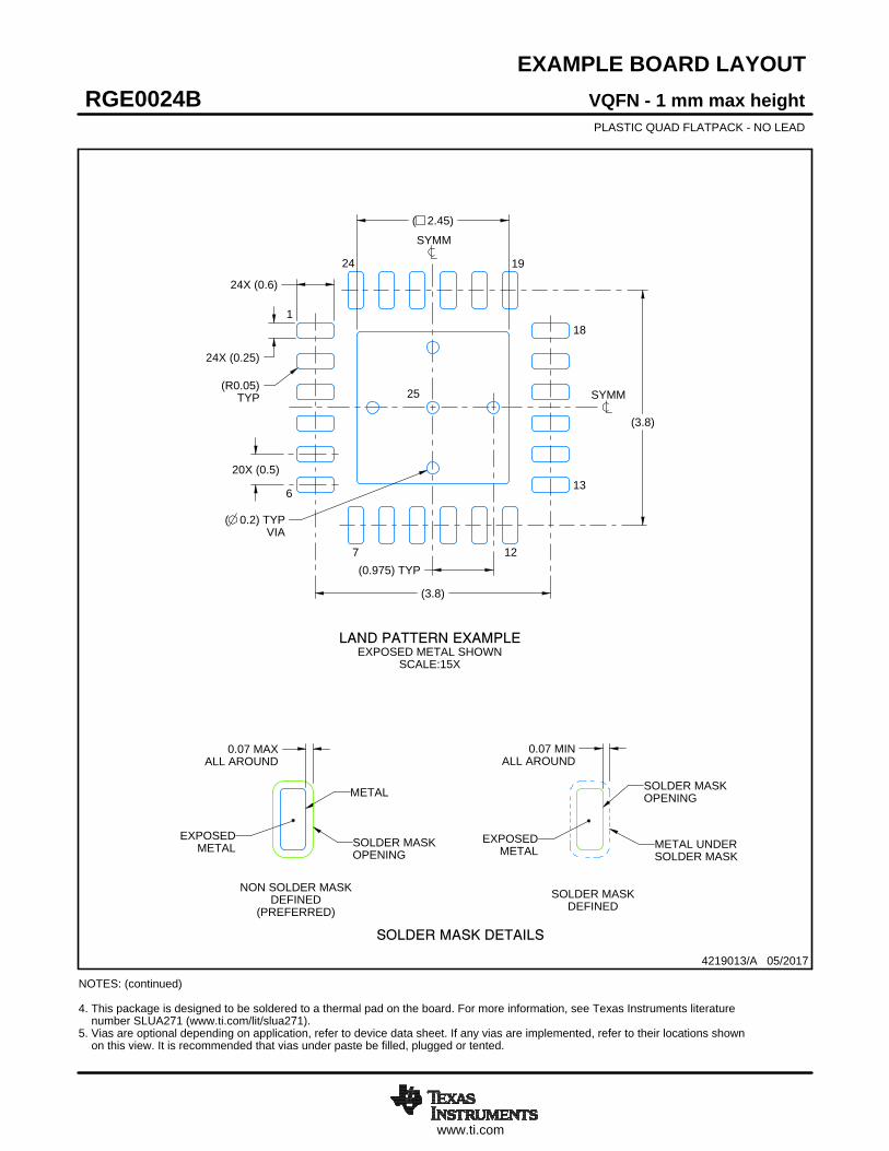
www.ti.com
EXAMPLE BOARD LAYOUT
0.07 MINALL AROUND
0.07 MAXALL AROUND
24X (0.25)
24X (0.6)
( 0.2) TYPVIA
20X (0.5)
(3.8)
(3.8)
( 2.45)
(R0.05)TYP
(0.975) TYP
VQFN - 1 mm max heightRGE0024BPLASTIC QUAD FLATPACK - NO LEAD
4219013/A 05/2017
SYMM
1
6
7 12
13
18
1924
SYMM
LAND PATTERN EXAMPLEEXPOSED METAL SHOWN
SCALE:15X
NOTES: (continued) 4. This package is designed to be soldered to a thermal pad on the board. For more information, see Texas Instruments literature number SLUA271 (www.ti.com/lit/slua271).5. Vias are optional depending on application, refer to device data sheet. If any vias are implemented, refer to their locations shown on this view. It is recommended that vias under paste be filled, plugged or tented.
25
SOLDER MASKOPENING
METAL UNDERSOLDER MASK
SOLDER MASKDEFINED
EXPOSEDMETAL
METAL
SOLDER MASKOPENING
SOLDER MASK DETAILS
NON SOLDER MASKDEFINED
(PREFERRED)
EXPOSEDMETAL
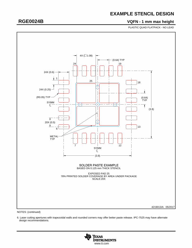
www.ti.com
EXAMPLE STENCIL DESIGN
24X (0.6)
24X (0.25)
20X (0.5)
(3.8)
(3.8)
4X ( 1.08)
(0.64)TYP
(0.64) TYP
(R0.05) TYP
VQFN - 1 mm max heightRGE0024BPLASTIC QUAD FLATPACK - NO LEAD
4219013/A 05/2017
NOTES: (continued) 6. Laser cutting apertures with trapezoidal walls and rounded corners may offer better paste release. IPC-7525 may have alternate design recommendations.
25
SYMM
METALTYP
SOLDER PASTE EXAMPLEBASED ON 0.125 mm THICK STENCIL
EXPOSED PAD 25
78% PRINTED SOLDER COVERAGE BY AREA UNDER PACKAGESCALE:20X
SYMM
1
6
7 12
13
18
1924
IMPORTANT NOTICE
Texas Instruments Incorporated (TI) reserves the right to make corrections, enhancements, improvements and other changes to itssemiconductor products and services per JESD46, latest issue, and to discontinue any product or service per JESD48, latest issue. Buyersshould obtain the latest relevant information before placing orders and should verify that such information is current and complete.TI’s published terms of sale for semiconductor products (http://www.ti.com/sc/docs/stdterms.htm) apply to the sale of packaged integratedcircuit products that TI has qualified and released to market. Additional terms may apply to the use or sale of other types of TI products andservices.Reproduction of significant portions of TI information in TI data sheets is permissible only if reproduction is without alteration and isaccompanied by all associated warranties, conditions, limitations, and notices. TI is not responsible or liable for such reproduceddocumentation. Information of third parties may be subject to additional restrictions. Resale of TI products or services with statementsdifferent from or beyond the parameters stated by TI for that product or service voids all express and any implied warranties for theassociated TI product or service and is an unfair and deceptive business practice. TI is not responsible or liable for any such statements.Buyers and others who are developing systems that incorporate TI products (collectively, “Designers”) understand and agree that Designersremain responsible for using their independent analysis, evaluation and judgment in designing their applications and that Designers havefull and exclusive responsibility to assure the safety of Designers' applications and compliance of their applications (and of all TI productsused in or for Designers’ applications) with all applicable regulations, laws and other applicable requirements. Designer represents that, withrespect to their applications, Designer has all the necessary expertise to create and implement safeguards that (1) anticipate dangerousconsequences of failures, (2) monitor failures and their consequences, and (3) lessen the likelihood of failures that might cause harm andtake appropriate actions. Designer agrees that prior to using or distributing any applications that include TI products, Designer willthoroughly test such applications and the functionality of such TI products as used in such applications.TI’s provision of technical, application or other design advice, quality characterization, reliability data or other services or information,including, but not limited to, reference designs and materials relating to evaluation modules, (collectively, “TI Resources”) are intended toassist designers who are developing applications that incorporate TI products; by downloading, accessing or using TI Resources in anyway, Designer (individually or, if Designer is acting on behalf of a company, Designer’s company) agrees to use any particular TI Resourcesolely for this purpose and subject to the terms of this Notice.TI’s provision of TI Resources does not expand or otherwise alter TI’s applicable published warranties or warranty disclaimers for TIproducts, and no additional obligations or liabilities arise from TI providing such TI Resources. TI reserves the right to make corrections,enhancements, improvements and other changes to its TI Resources. TI has not conducted any testing other than that specificallydescribed in the published documentation for a particular TI Resource.Designer is authorized to use, copy and modify any individual TI Resource only in connection with the development of applications thatinclude the TI product(s) identified in such TI Resource. NO OTHER LICENSE, EXPRESS OR IMPLIED, BY ESTOPPEL OR OTHERWISETO ANY OTHER TI INTELLECTUAL PROPERTY RIGHT, AND NO LICENSE TO ANY TECHNOLOGY OR INTELLECTUAL PROPERTYRIGHT OF TI OR ANY THIRD PARTY IS GRANTED HEREIN, including but not limited to any patent right, copyright, mask work right, orother intellectual property right relating to any combination, machine, or process in which TI products or services are used. Informationregarding or referencing third-party products or services does not constitute a license to use such products or services, or a warranty orendorsement thereof. Use of TI Resources may require a license from a third party under the patents or other intellectual property of thethird party, or a license from TI under the patents or other intellectual property of TI.TI RESOURCES ARE PROVIDED “AS IS” AND WITH ALL FAULTS. TI DISCLAIMS ALL OTHER WARRANTIES ORREPRESENTATIONS, EXPRESS OR IMPLIED, REGARDING RESOURCES OR USE THEREOF, INCLUDING BUT NOT LIMITED TOACCURACY OR COMPLETENESS, TITLE, ANY EPIDEMIC FAILURE WARRANTY AND ANY IMPLIED WARRANTIES OFMERCHANTABILITY, FITNESS FOR A PARTICULAR PURPOSE, AND NON-INFRINGEMENT OF ANY THIRD PARTY INTELLECTUALPROPERTY RIGHTS. TI SHALL NOT BE LIABLE FOR AND SHALL NOT DEFEND OR INDEMNIFY DESIGNER AGAINST ANY CLAIM,INCLUDING BUT NOT LIMITED TO ANY INFRINGEMENT CLAIM THAT RELATES TO OR IS BASED ON ANY COMBINATION OFPRODUCTS EVEN IF DESCRIBED IN TI RESOURCES OR OTHERWISE. IN NO EVENT SHALL TI BE LIABLE FOR ANY ACTUAL,DIRECT, SPECIAL, COLLATERAL, INDIRECT, PUNITIVE, INCIDENTAL, CONSEQUENTIAL OR EXEMPLARY DAMAGES INCONNECTION WITH OR ARISING OUT OF TI RESOURCES OR USE THEREOF, AND REGARDLESS OF WHETHER TI HAS BEENADVISED OF THE POSSIBILITY OF SUCH DAMAGES.Unless TI has explicitly designated an individual product as meeting the requirements of a particular industry standard (e.g., ISO/TS 16949and ISO 26262), TI is not responsible for any failure to meet such industry standard requirements.Where TI specifically promotes products as facilitating functional safety or as compliant with industry functional safety standards, suchproducts are intended to help enable customers to design and create their own applications that meet applicable functional safety standardsand requirements. Using products in an application does not by itself establish any safety features in the application. Designers mustensure compliance with safety-related requirements and standards applicable to their applications. Designer may not use any TI products inlife-critical medical equipment unless authorized officers of the parties have executed a special contract specifically governing such use.Life-critical medical equipment is medical equipment where failure of such equipment would cause serious bodily injury or death (e.g., lifesupport, pacemakers, defibrillators, heart pumps, neurostimulators, and implantables). Such equipment includes, without limitation, allmedical devices identified by the U.S. Food and Drug Administration as Class III devices and equivalent classifications outside the U.S.TI may expressly designate certain products as completing a particular qualification (e.g., Q100, Military Grade, or Enhanced Product).Designers agree that it has the necessary expertise to select the product with the appropriate qualification designation for their applicationsand that proper product selection is at Designers’ own risk. Designers are solely responsible for compliance with all legal and regulatoryrequirements in connection with such selection.Designer will fully indemnify TI and its representatives against any damages, costs, losses, and/or liabilities arising out of Designer’s non-compliance with the terms and provisions of this Notice.
Mailing Address: Texas Instruments, Post Office Box 655303, Dallas, Texas 75265Copyright © 2018, Texas Instruments Incorporated