Embed Size (px)
Citation preview
1SLVUAX8–November 2016Submit Documentation Feedback
Copyright © 2016, Texas Instruments Incorporated
TPS54824EVM-779 8-A, SWIFT™ Regulator Evaluation Module
User's GuideSLVUAX8–November 2016
TPS54824EVM-779 8-A, SWIFT™ RegulatorEvaluation Module
This user’s guide contains information for the TPS54824EVM-779 evaluation module (PWR779) as well asfor the TPS54824 dc/dc converter. Also included are the performance specifications, the schematic, andthe bill of materials for the TPS54824EVM-779.
Contents1 Introduction ................................................................................................................... 2
1.1 Background .......................................................................................................... 21.2 Performance Specification Summary ............................................................................ 21.3 Modifications......................................................................................................... 3
2 Test Setup and Results ..................................................................................................... 42.1 Input/Output Connections.......................................................................................... 42.2 Efficiency............................................................................................................. 52.3 Output Voltage Load Regulation.................................................................................. 72.4 Output Voltage Line Regulation................................................................................... 72.5 Load Transients ..................................................................................................... 82.6 Loop Characteristics................................................................................................ 82.7 Output Voltage Ripple.............................................................................................. 92.8 Input Voltage Ripple .............................................................................................. 102.9 Powering Up ....................................................................................................... 112.10 Powering Down.................................................................................................... 122.11 Start-Up Into Pre-Bias ............................................................................................ 132.12 Hiccup Mode Current Limit....................................................................................... 14
3 Board Layout................................................................................................................ 163.1 Layout............................................................................................................... 16
4 Schematic and Bill of Materials........................................................................................... 194.1 Schematic .......................................................................................................... 194.2 Bill of Materials .................................................................................................... 20
List of Figures
1 TPS54824EVM-779 Efficiency - Cyntec Inductor ....................................................................... 52 TPS54824EVM-779 Low Current Efficiency - Cyntec Inductor........................................................ 53 TPS54824EVM-779 Efficiency - Wurth Electronics 744311100 Inductor ............................................ 64 TPS54824EVM-779 Load Regulation..................................................................................... 75 TPS54824EVM-779 Line Regulation...................................................................................... 76 TPS54824EVM-779 Transient Response ................................................................................ 87 TPS54824EVM-779 Loop Response ..................................................................................... 88 TPS54824EVM-779 Output Ripple, No Load ............................................................................ 99 TPS54824EVM-779 Output Ripple, 8-A Load ........................................................................... 910 TPS54824EVM-779 Input Ripple, No Load............................................................................. 1011 TPS54824EVM-779 Input Ripple, 8-A Load ............................................................................ 1012 TPS54824EVM-779 Start-Up Relative to VIN ........................................................................... 1113 TPS54824EVM-779 Start-Up Relative to Enable ...................................................................... 1114 TPS54824EVM-779 Shutdown Relative to VIN ......................................................................... 12

Introduction www.ti.com
2 SLVUAX8–November 2016Submit Documentation Feedback
Copyright © 2016, Texas Instruments Incorporated
TPS54824EVM-779 8-A, SWIFT™ Regulator Evaluation Module
15 TPS54824EVM-779 Shutdown Relative to Enable .................................................................... 1216 TPS54824EVM-779 Start-Up Into Pre-Bias ............................................................................ 1317 TPS54824EVM-779 Hiccup Mode Current Limit....................................................................... 1418 TPS54824EVM-779 Hiccup Mode Start................................................................................. 1419 TPS54824EVM-779 Hiccup Mode Stop................................................................................. 1520 TPS54824EVM-779 Top-Side Layout ................................................................................... 1721 TPS54824EVM-779 Internal Layer-1 Layout ........................................................................... 1722 TPS54824EVM-779 Internal Layer-2 Layout ........................................................................... 1823 TPS54824EVM-779 Bottom-Side Layout ............................................................................... 1824 TPS54824EVM-779 Schematic .......................................................................................... 19
List of Tables
1 Input Voltage and Output Current Summary ............................................................................. 22 TPS54824EVM-779 Performance Specification Summary ............................................................ 23 TPS54824EVM-779 EVM Connectors and Test Points ................................................................ 44 TPS54824EVM-779 Bill of Materials..................................................................................... 20
TrademarksAll trademarks are the property of their respective owners.
1 Introduction
1.1 BackgroundThe TPS54824 dc/dc converter is a synchronous buck converter designed to provide up to an 8-A output.The input (VIN) is rated for 4.5 V to 17 V. Rated input voltage and output current range for the evaluationmodule are given in Table 1. This evaluation module is designed to demonstrate the small printed-circuit-board areas that may be achieved when designing with the TPS54824 regulator. The RT/CLK pin isconfigured for 700-kHz switching frequency. The high-side and low-side MOSFETs are incorporated insidethe TPS54824 package along with the gate-drive circuitry. The low drain-to-source on-resistance of theMOSFET allows the TPS54824 to achieve high efficiencies and helps keep the junction temperature lowat high output currents. An external divider allows for an adjustable output voltage. Additionally, theTPS54824 provides adjustable soft start and undervoltage lockout inputs and a power good output.
Table 1. Input Voltage and Output Current Summary
EVM Input Voltage Range Output Current RangeTPS54824EVM-779 VIN = 4.5 V to 17 V 0 A to 8 A
1.2 Performance Specification SummaryA summary of the TPS54824EVM-779 performance specifications is provided in Table 2. Specificationsare given for an input voltage of VIN = 12 V and an output voltage of 1.8 V, unless otherwise specified. TheTPS54824EVM-779 is designed and tested for VIN = 4.5 V to 17 V. The ambient temperature is 25°C forall measurements, unless otherwise noted.
Table 2. TPS54824EVM-779 Performance Specification Summary
Specification Test Conditions MIN TYP MAX UnitVIN voltage range 4.5 12 17 VVIN start voltage 4.4 VVIN stop voltage 4 VOutput voltage setpoint 1.8 VOutput current range VIN = 4.5 V to 17 V 0 8 ALoad regulation VIN = 4.5 V to 17 V, IO = 8 A –0.1%
www.ti.com Introduction
3SLVUAX8–November 2016Submit Documentation Feedback
Copyright © 2016, Texas Instruments Incorporated
TPS54824EVM-779 8-A, SWIFT™ Regulator Evaluation Module
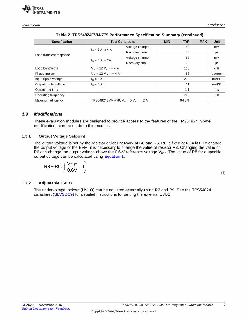
Table 2. TPS54824EVM-779 Performance Specification Summary (continued)Specification Test Conditions MIN TYP MAX Unit
Load transient responseIO = 2 A to 6 A
Voltage change –50 mVRecovery time 75 µs
IO = 6 A to 2AVoltage change 55 mVRecovery time 75 µs
Loop bandwidth VIN = 12 V, IO = 4 A 116 kHzPhase margin VIN = 12 V , IO = 4 A 58 degreeInput ripple voltage IO = 8 A 270 mVPPOutput ripple voltage IO = 8 A 11 mVPPOutput rise time 1.1 msOperating frequency 700 kHzMaximum efficiency TPS54824EVM-779, VIN = 5 V, IO = 2 A 94.3%
1.3 ModificationsThese evaluation modules are designed to provide access to the features of the TPS54824. Somemodifications can be made to this module.
1.3.1 Output Voltage SetpointThe output voltage is set by the resistor divider network of R8 and R6. R6 is fixed at 6.04 kΩ. To changethe output voltage of the EVM, it is necessary to change the value of resistor R8. Changing the value ofR6 can change the output voltage above the 0.6-V reference voltage VREF. The value of R8 for a specificoutput voltage can be calculated using Equation 1.
(1)
1.3.2 Adjustable UVLOThe undervoltage lockout (UVLO) can be adjusted externally using R2 and R9. See the TPS54824datasheet (SLVSDC9) for detailed instructions for setting the external UVLO.

Test Setup and Results www.ti.com
4 SLVUAX8–November 2016Submit Documentation Feedback
Copyright © 2016, Texas Instruments Incorporated
TPS54824EVM-779 8-A, SWIFT™ Regulator Evaluation Module
2 Test Setup and ResultsThis section describes how to properly connect, set up, and use the TPS54824EVM-779 evaluationmodule. The section also includes test results typical for the evaluation module and covers efficiency,output voltage regulation, load transients, loop response, output ripple, input ripple, start-up, and currentlimit modes.
2.1 Input/Output ConnectionsThe TPS54824EVM-779 is provided with input/output connectors and test points as shown in Table 3. Apower supply capable of supplying greater than 5 A must be connected to J1 through a pair of 20-AWGwires or better. The load must be connected to J2 through a pair of 20-AWG wires or better. Themaximum load current capability is 12 A. Wire lengths must be minimized to reduce losses in the wires.Test point TP1 provides a place to monitor the VIN input voltages with TP7 providing a convenient groundreference. TP4 is used to monitor the output voltage with TP9 as the ground reference.
Table 3. TPS54824EVM-779 EVM Connectors and Test Points
Reference Designator FunctionJ1 VIN input voltage connector (see Table 1 for VIN range)J2 VOUT terminal to connect loadJ3 2-pin header for enable. Add shunt to connect EN to ground and disable device.J4 2-pin header for power good resistor pullup connection. Add a shunt to pull up to VOUT.
TP1 VIN test pointTP2 EN test pointTP3 SW node test pointTP4 1.8-V test pointTP5 PGOOD pullup test pointTP6 PGOOD test pointTP7 PGND test pointTP8 SS/TRK test pointTP9 PGND test point
TP10 Test point between voltage divider network and output of TPS54824 converter. Used for loop responsemeasurements.
TP11 PGND test pointTP12 AGND test pointTP13 AGND test pointTP14 PGND test pointTP15 Test point for supplying external CLK for synchronization. C20 and R10 should be populated to use.

Output Current (A)
Effi
cien
cy (
%)
0.001 0.002 0.003 0.005 0.01 0.02 0.03 0.05 0.07 0.1 0.2 0.3 0.40.5 0.7 1 2 3 4 5 6 7 80
10
20
30
40
50
60
70
80
90
100
D004
VIN = 5VVIN = 12VVIN = 17V
Output Current (A)
Effi
cien
cy (
%)
0 1 2 3 4 5 6 7 850
60
70
80
90
100
D001
VIN = 5VVIN = 12VVIN = 17V
www.ti.com Test Setup and Results
5SLVUAX8–November 2016Submit Documentation Feedback
Copyright © 2016, Texas Instruments Incorporated
TPS54824EVM-779 8-A, SWIFT™ Regulator Evaluation Module
2.2 EfficiencyThe efficiency of this EVM peaks at a load current of about 4 A and then decreases as the load currentincreases toward full load. Figure 1 shows the efficiency for the TPS54824EVM-779 at an ambienttemperature of 25°C.
Figure 1. TPS54824EVM-779 Efficiency - Cyntec Inductor
Figure 2 shows the efficiency for the TPS54824EVM-779 using a semi-log scale to more easily showefficiency at lower output currents. The ambient temperature is 25°C.
Figure 2. TPS54824EVM-779 Low Current Efficiency - Cyntec Inductor

Output Current (A)
Effi
cien
cy (
%)
0 1 2 3 4 5 6 7 850
60
70
80
90
100
D002
VIN = 5VVIN = 12VVIN = 17V
Test Setup and Results www.ti.com
6 SLVUAX8–November 2016Submit Documentation Feedback
Copyright © 2016, Texas Instruments Incorporated
TPS54824EVM-779 8-A, SWIFT™ Regulator Evaluation Module
Figure 3 shows the efficiency for the TPS54824EVM-779 with a WE 744311100 inductor. The ambienttemperature is 25°C.
Figure 3. TPS54824EVM-779 Efficiency - Wurth Electronics 744311100 Inductor
The efficiency may be lower at higher ambient temperatures, due to temperature variation in the drain-to-source resistance of the internal MOSFETs.

Input Voltage (V)
Line
Reg
ulat
ion
(%)
4.5 5.5 6.5 7.5 8.5 9.5 10.5 11.5 12.5 13.5 14.5 15.5 16.5 17-0.50
-0.40
-0.30
-0.20
-0.10
0.00
0.10
0.20
0.30
0.40
0.50
D006
IOUT = 0AIOUT = 4AIOUT = 8A
Output Current (A)
Load
Reg
ulat
ion
(%)
0 1 2 3 4 5 6 7 8-0.50
-0.40
-0.30
-0.20
-0.10
0.00
0.10
0.20
0.30
0.40
0.50
D005D006
VIN = 5VVIN = 12VVIN = 17V
www.ti.com Test Setup and Results
7SLVUAX8–November 2016Submit Documentation Feedback
Copyright © 2016, Texas Instruments Incorporated
TPS54824EVM-779 8-A, SWIFT™ Regulator Evaluation Module
2.3 Output Voltage Load RegulationFigure 4 shows the load regulation for the TPS54824EVM-779.
Figure 4. TPS54824EVM-779 Load Regulation
Measurements are given for an ambient temperature of 25°C.
2.4 Output Voltage Line RegulationFigure 5 shows the line regulation for the TPS54824EVM-779.
Figure 5. TPS54824EVM-779 Line Regulation
Frequency (Hz)
Gai
n (d
B)
Pha
se (
Deg
ree)
100 200 300 500 700 1000 2000 3000 5000 10000 2000030000 50000 100000 200000 500000-70 -210
-60 -180
-50 -150
-40 -120
-30 -90
-20 -60
-10 -30
0 0
10 30
20 60
30 90
40 120
50 150
60 180
70 210
D007
Gain (dB)Phase (Deg)
Test Setup and Results www.ti.com
8 SLVUAX8–November 2016Submit Documentation Feedback
Copyright © 2016, Texas Instruments Incorporated
TPS54824EVM-779 8-A, SWIFT™ Regulator Evaluation Module
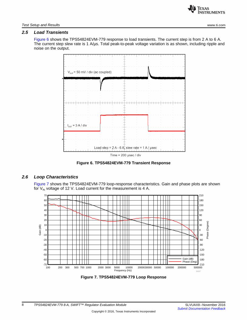
2.5 Load TransientsFigure 6 shows the TPS54824EVM-779 response to load transients. The current step is from 2 A to 6 A.The current step slew rate is 1 A/µs. Total peak-to-peak voltage variation is as shown, including ripple andnoise on the output.
Figure 6. TPS54824EVM-779 Transient Response
2.6 Loop CharacteristicsFigure 7 shows the TPS54824EVM-779 loop-response characteristics. Gain and phase plots are shownfor VIN voltage of 12 V. Load current for the measurement is 4 A.
Figure 7. TPS54824EVM-779 Loop Response

www.ti.com Test Setup and Results
9SLVUAX8–November 2016Submit Documentation Feedback
Copyright © 2016, Texas Instruments Incorporated
TPS54824EVM-779 8-A, SWIFT™ Regulator Evaluation Module
2.7 Output Voltage RippleFigure 8 and Figure 9 show the TPS54824EVM-779 output voltage ripple. The load currents are no loadand 8 A. VIN = 12 V. The ripple voltage is measured directly across TP9 and TP4.
Figure 8. TPS54824EVM-779 Output Ripple, No Load
Figure 9. TPS54824EVM-779 Output Ripple, 8-A Load

Test Setup and Results www.ti.com
10 SLVUAX8–November 2016Submit Documentation Feedback
Copyright © 2016, Texas Instruments Incorporated
TPS54824EVM-779 8-A, SWIFT™ Regulator Evaluation Module
2.8 Input Voltage RippleFigure 10 and Figure 11 show the TPS54824EVM-779 input voltage ripple. The load currents are no loadand 8 A. VIN = 12 V. The ripple voltage is measured directly across TP1 and TP7.
Figure 10. TPS54824EVM-779 Input Ripple, No Load
Figure 11. TPS54824EVM-779 Input Ripple, 8-A Load

www.ti.com Test Setup and Results
11SLVUAX8–November 2016Submit Documentation Feedback
Copyright © 2016, Texas Instruments Incorporated
TPS54824EVM-779 8-A, SWIFT™ Regulator Evaluation Module
2.9 Powering UpFigure 12 and Figure 13 show the start-up waveforms for the TPS54824EVM-779. In Figure 12, the outputvoltage ramps up as soon as the input voltage reaches the UVLO threshold. In Figure 13, the inputvoltage is initially applied and the output is inhibited by pulling EN to GND using an external functiongenerator. When the EN voltage is increased above the enable-threshold voltage, the start-up sequencebegins and the output voltage ramps up to the externally set value of 1.8 V. The input voltage for theseplots is 12 V and the load is 1 Ω. Alternatively, a jumper at J3 to tie EN to GND can also be used. Whenthe jumper is removed, EN is released and the start-up sequence will begin.
Figure 12. TPS54824EVM-779 Start-Up Relative to VIN
Figure 13. TPS54824EVM-779 Start-Up Relative to Enable

Test Setup and Results www.ti.com
12 SLVUAX8–November 2016Submit Documentation Feedback
Copyright © 2016, Texas Instruments Incorporated
TPS54824EVM-779 8-A, SWIFT™ Regulator Evaluation Module
2.10 Powering DownFigure 14 and Figure 15 show the TPS54824EVM-779 shutdown. The input voltage for these plots is 12 Vand the load is 1 Ω.
Figure 14. TPS54824EVM-779 Shutdown Relative to VIN
Figure 15. TPS54824EVM-779 Shutdown Relative to Enable

www.ti.com Test Setup and Results
13SLVUAX8–November 2016Submit Documentation Feedback
Copyright © 2016, Texas Instruments Incorporated
TPS54824EVM-779 8-A, SWIFT™ Regulator Evaluation Module
2.11 Start-Up Into Pre-BiasFigure 16 shows the TPS54824EVM-779 start up into a pre-biased output. The output voltage is pre-biased to 1 V.
Figure 16. TPS54824EVM-779 Start-Up Into Pre-Bias
Test Setup and Results www.ti.com
14 SLVUAX8–November 2016Submit Documentation Feedback
Copyright © 2016, Texas Instruments Incorporated
TPS54824EVM-779 8-A, SWIFT™ Regulator Evaluation Module
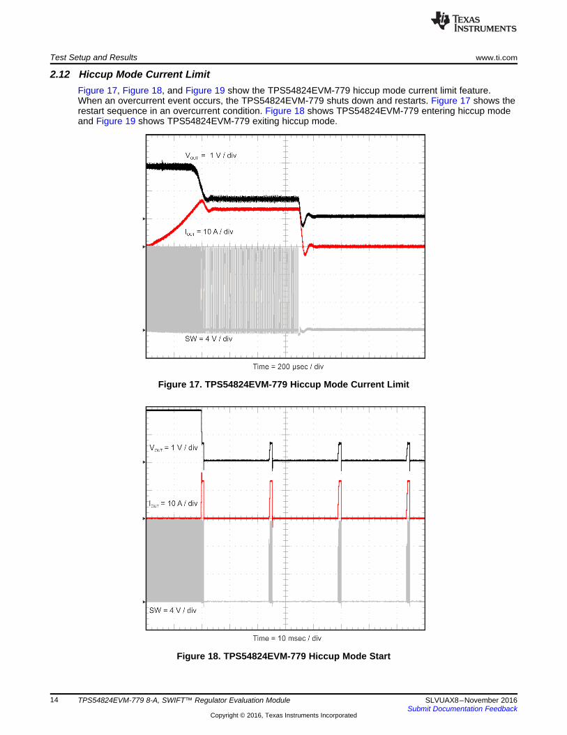
2.12 Hiccup Mode Current LimitFigure 17, Figure 18, and Figure 19 show the TPS54824EVM-779 hiccup mode current limit feature.When an overcurrent event occurs, the TPS54824EVM-779 shuts down and restarts. Figure 17 shows therestart sequence in an overcurrent condition. Figure 18 shows TPS54824EVM-779 entering hiccup modeand Figure 19 shows TPS54824EVM-779 exiting hiccup mode.
Figure 17. TPS54824EVM-779 Hiccup Mode Current Limit
Figure 18. TPS54824EVM-779 Hiccup Mode Start

www.ti.com Test Setup and Results
15SLVUAX8–November 2016Submit Documentation Feedback
Copyright © 2016, Texas Instruments Incorporated
TPS54824EVM-779 8-A, SWIFT™ Regulator Evaluation Module
Figure 19. TPS54824EVM-779 Hiccup Mode Stop
Board Layout www.ti.com
16 SLVUAX8–November 2016Submit Documentation Feedback
Copyright © 2016, Texas Instruments Incorporated
TPS54824EVM-779 8-A, SWIFT™ Regulator Evaluation Module
3 Board LayoutThis section provides a description of the TPS54824EVM-779 board layout and layer illustrations.
3.1 LayoutThe board layout for the TPS54824EVM-779 is shown in Figure 20 through Figure 23. The top-side layerof the EVM is laid out in a manner typical of a user application. The top, bottom, and internal layers are2-oz. copper.
The top layer contains the main power traces for VIN, VOUT, and SW. Also on the top layer areconnections for the remaining pins of the TPS54824 and the majority of the signal traces. The top layerhas dedicated ground plane for quiet analog ground that is connected to the main power ground plane ata single point. The internal layer-1 is a large ground plane and also routes signals to test points. Theinternal layer-2 contains an additional large ground copper area as well as an additional VIN and VOUTcopper fill. The bottom layer is another ground plane with two additional traces for the output voltagefeedback. The top-side ground traces are connected to the bottom and internal ground planes withmultiple vias placed around the board.
The input decoupling capacitors and bootstrap capacitor are all located as close to the IC as possible.Additionally, the voltage set point resistor divider components are kept close to the IC. The voltage dividernetwork ties to the output voltage at the point of regulation, the copper VOUT trace at the TP4 test point. Anadditional input bulk capacitor is used to limit the noise entering the converter from the input supply.Critical analog circuits such as the voltage set point divider, EN resistor, SS/TRK capacitor, RT/CLKresistor, and COMP pin are terminated to the quiet analog ground island on the top layer.

www.ti.com Board Layout
17SLVUAX8–November 2016Submit Documentation Feedback
Copyright © 2016, Texas Instruments Incorporated
TPS54824EVM-779 8-A, SWIFT™ Regulator Evaluation Module
Figure 20. TPS54824EVM-779 Top-Side Layout
Figure 21. TPS54824EVM-779 Internal Layer-1 Layout

Board Layout www.ti.com
18 SLVUAX8–November 2016Submit Documentation Feedback
Copyright © 2016, Texas Instruments Incorporated
TPS54824EVM-779 8-A, SWIFT™ Regulator Evaluation Module
Figure 22. TPS54824EVM-779 Internal Layer-2 Layout
Figure 23. TPS54824EVM-779 Bottom-Side Layout

www.ti.com Schematic and Bill of Materials
19SLVUAX8–November 2016Submit Documentation Feedback
Copyright © 2016, Texas Instruments Incorporated
TPS54824EVM-779 8-A, SWIFT™ Regulator Evaluation Module
4 Schematic and Bill of MaterialsThis section presents the TPS54824EVM-779 schematic and bill of materials.
4.1 SchematicFigure 24 is the schematic for the TPS54824EVM-779.
Figure 24. TPS54824EVM-779 Schematic

Schematic and Bill of Materials www.ti.com
20 SLVUAX8–November 2016Submit Documentation Feedback
Copyright © 2016, Texas Instruments Incorporated
TPS54824EVM-779 8-A, SWIFT™ Regulator Evaluation Module
4.2 Bill of MaterialsTable 4 presents the bill of materials for the TPS54824EVM-779.
Table 4. TPS54824EVM-779 Bill of MaterialsDesignator Qty Value Description Package Reference Part Number Manufacturer
C3, C4 2 10uF CAP, CERM, 10 µF, 35 V, +/- 20%, X5R, 1206 1206 C3216X5R1V106M160AB TDK
C5, C6, C8 3 0.1uF CAP, CERM, 0.1uF, 25V, +/-10%, X7R, 0603 0603 06033C104KAT2A AVX
C7 1 100uF CAP, AL, 100 µF, 50 V, +/- 20%, 0.18 ohm, TH Cap, 10x12.5mm UBT1H101MPD1TD Nichicon
C9, C10, C11, C12 4 47uF CAP, CERM, 47 µF, 6.3 V, +/- 20%, X5R, 1206 1206 GRM31CR60J476ME19L Murata
C16 1 8200pF CAP, CERM, 8200 pF, 25 V, +/- 10%, X7R, 0603 0603 GRM188R71E822KA01D Murata
C17 1 27pF CAP, CERM, 27 pF, 50 V, +/- 5%, C0G/NP0, 0603 0603 GRM1885C1H270JA01D Murata
C18 1 2200pF CAP, CERM, 2200 pF, 25 V, +/- 10%, X7R, 0603 0603 GRM188R71E222KA01D Murata
C19 1 100pF CAP, CERM, 100 pF, 50 V, +/- 5%, C0G/NP0, 0603 0603 885012006057 Wurth Elektronik
J1, J2 2 Terminal Block, 5.08 mm, 2x1, Brass, TH 2x1 5.08 mm Terminal Block ED120/2DS On-Shore Technology
J3, J4 2 Header, 100mil, 2x1, Gold, TH Header, 100mil, 2x1, TH HTSW-102-07-G-S Samtec
L1 1 1uH Inductor, 1 µH, 14.4 A, 0.0064 ohm, SMD 6.95x2.8x6.6mm CMLE063T-1R0MS Cyntec
LBL1 1 Thermal Transfer Printable Labels, 0.650" W x 0.200" H - 10,000per roll
PCB Label 0.650"H x 0.200"W THT-14-423-10 Brady
R1 1 100k RES, 100 k, 5%, 0.1 W, 0603 0603 CRCW0603100KJNEA Vishay-Dale
R2 1 86.6k RES, 86.6 k, 1%, 0.1 W, 0603 0603 CRCW060386K6FKEA Vishay-Dale
R4 1 10 RES, 10, 5%, 0.1 W, 0603 0603 CRCW060310R0JNEA Vishay-Dale
R5 1 9.53k RES, 9.53 k, 1%, 0.1 W, 0603 0603 CRCW06039K53FKEA Vishay-Dale
R6 1 6.04k RES, 6.04 k, 1%, 0.1 W, 0603 0603 CRCW06036K04FKEA Vishay-Dale
R7 1 69.8k RES, 69.8 k, 1%, 0.1 W, 0603 0603 CRCW060369K8FKEA Vishay-Dale
R8 1 12.1k RES, 12.1 k, 1%, 0.1 W, 0603 0603 CRCW060312K1FKEA Vishay-Dale
R9 1 30.9k RES, 30.9 k, 1%, 0.1 W, 0603 0603 CRCW060330K9FKEA Vishay-Dale
SH-J1, SH-J2 2 1x2 Shunt, 100mil, Gold plated, Black Shunt SNT-100-BK-G Samtec
TP1, TP2, TP3, TP4,TP5, TP6, TP7, TP8,TP9, TP10, TP11, TP12,TP13, TP14, TP15
15 Test Point, Miniature, SMT Testpoint_Keystone_Miniature 5015 Keystone
U1 1 4.5-V to 17-V Input, 8-A Synchronous Step-Down VoltageRegulator, RNV0018B (VQFN-HR-18)
RNV0018B TPS54824RNVR Texas Instruments
C1, C2 0 22uF CAP, CERM, 22 µF, 35 V, +/- 20%, X5R, 1206 1206 C3216X5R1V226M160AC TDK
C20 0 47pF CAP, CERM, 47 pF, 50 V, +/- 5%, C0G/NP0, 0603 0603 06035A470JAT2A AVX
FID1, FID2, FID3 0 Fiducial mark. There is nothing to buy or mount. Fiducial N/A N/A
R10 0 2.00k RES, 2.00 k, 1%, 0.1 W, 0603 0603 CRCW06032K00FKEA Vishay-Dale

STANDARD TERMS AND CONDITIONS FOR EVALUATION MODULES1. Delivery: TI delivers TI evaluation boards, kits, or modules, including demonstration software, components, and/or documentation
which may be provided together or separately (collectively, an “EVM” or “EVMs”) to the User (“User”) in accordance with the termsand conditions set forth herein. Acceptance of the EVM is expressly subject to the following terms and conditions.1.1 EVMs are intended solely for product or software developers for use in a research and development setting to facilitate feasibility
evaluation, experimentation, or scientific analysis of TI semiconductors products. EVMs have no direct function and are notfinished products. EVMs shall not be directly or indirectly assembled as a part or subassembly in any finished product. Forclarification, any software or software tools provided with the EVM (“Software”) shall not be subject to the terms and conditionsset forth herein but rather shall be subject to the applicable terms and conditions that accompany such Software
1.2 EVMs are not intended for consumer or household use. EVMs may not be sold, sublicensed, leased, rented, loaned, assigned,or otherwise distributed for commercial purposes by Users, in whole or in part, or used in any finished product or productionsystem.
2 Limited Warranty and Related Remedies/Disclaimers:2.1 These terms and conditions do not apply to Software. The warranty, if any, for Software is covered in the applicable Software
License Agreement.2.2 TI warrants that the TI EVM will conform to TI's published specifications for ninety (90) days after the date TI delivers such EVM
to User. Notwithstanding the foregoing, TI shall not be liable for any defects that are caused by neglect, misuse or mistreatmentby an entity other than TI, including improper installation or testing, or for any EVMs that have been altered or modified in anyway by an entity other than TI. Moreover, TI shall not be liable for any defects that result from User's design, specifications orinstructions for such EVMs. Testing and other quality control techniques are used to the extent TI deems necessary or asmandated by government requirements. TI does not test all parameters of each EVM.
2.3 If any EVM fails to conform to the warranty set forth above, TI's sole liability shall be at its option to repair or replace such EVM,or credit User's account for such EVM. TI's liability under this warranty shall be limited to EVMs that are returned during thewarranty period to the address designated by TI and that are determined by TI not to conform to such warranty. If TI elects torepair or replace such EVM, TI shall have a reasonable time to repair such EVM or provide replacements. Repaired EVMs shallbe warranted for the remainder of the original warranty period. Replaced EVMs shall be warranted for a new full ninety (90) daywarranty period.
3 Regulatory Notices:3.1 United States
3.1.1 Notice applicable to EVMs not FCC-Approved:This kit is designed to allow product developers to evaluate electronic components, circuitry, or software associated with the kitto determine whether to incorporate such items in a finished product and software developers to write software applications foruse with the end product. This kit is not a finished product and when assembled may not be resold or otherwise marketed unlessall required FCC equipment authorizations are first obtained. Operation is subject to the condition that this product not causeharmful interference to licensed radio stations and that this product accept harmful interference. Unless the assembled kit isdesigned to operate under part 15, part 18 or part 95 of this chapter, the operator of the kit must operate under the authority ofan FCC license holder or must secure an experimental authorization under part 5 of this chapter.3.1.2 For EVMs annotated as FCC – FEDERAL COMMUNICATIONS COMMISSION Part 15 Compliant:
CAUTIONThis device complies with part 15 of the FCC Rules. Operation is subject to the following two conditions: (1) This device may notcause harmful interference, and (2) this device must accept any interference received, including interference that may causeundesired operation.Changes or modifications not expressly approved by the party responsible for compliance could void the user's authority tooperate the equipment.
FCC Interference Statement for Class A EVM devicesNOTE: This equipment has been tested and found to comply with the limits for a Class A digital device, pursuant to part 15 ofthe FCC Rules. These limits are designed to provide reasonable protection against harmful interference when the equipment isoperated in a commercial environment. This equipment generates, uses, and can radiate radio frequency energy and, if notinstalled and used in accordance with the instruction manual, may cause harmful interference to radio communications.Operation of this equipment in a residential area is likely to cause harmful interference in which case the user will be required tocorrect the interference at his own expense.
SPACER
SPACER
SPACER
SPACER
SPACER
SPACER
SPACER
SPACER
FCC Interference Statement for Class B EVM devicesNOTE: This equipment has been tested and found to comply with the limits for a Class B digital device, pursuant to part 15 ofthe FCC Rules. These limits are designed to provide reasonable protection against harmful interference in a residentialinstallation. This equipment generates, uses and can radiate radio frequency energy and, if not installed and used in accordancewith the instructions, may cause harmful interference to radio communications. However, there is no guarantee that interferencewill not occur in a particular installation. If this equipment does cause harmful interference to radio or television reception, whichcan be determined by turning the equipment off and on, the user is encouraged to try to correct the interference by one or moreof the following measures:
• Reorient or relocate the receiving antenna.• Increase the separation between the equipment and receiver.• Connect the equipment into an outlet on a circuit different from that to which the receiver is connected.• Consult the dealer or an experienced radio/TV technician for help.
3.2 Canada3.2.1 For EVMs issued with an Industry Canada Certificate of Conformance to RSS-210
Concerning EVMs Including Radio Transmitters:This device complies with Industry Canada license-exempt RSS standard(s). Operation is subject to the following two conditions:(1) this device may not cause interference, and (2) this device must accept any interference, including interference that maycause undesired operation of the device.
Concernant les EVMs avec appareils radio:Le présent appareil est conforme aux CNR d'Industrie Canada applicables aux appareils radio exempts de licence. L'exploitationest autorisée aux deux conditions suivantes: (1) l'appareil ne doit pas produire de brouillage, et (2) l'utilisateur de l'appareil doitaccepter tout brouillage radioélectrique subi, même si le brouillage est susceptible d'en compromettre le fonctionnement.
Concerning EVMs Including Detachable Antennas:Under Industry Canada regulations, this radio transmitter may only operate using an antenna of a type and maximum (or lesser)gain approved for the transmitter by Industry Canada. To reduce potential radio interference to other users, the antenna typeand its gain should be so chosen that the equivalent isotropically radiated power (e.i.r.p.) is not more than that necessary forsuccessful communication. This radio transmitter has been approved by Industry Canada to operate with the antenna typeslisted in the user guide with the maximum permissible gain and required antenna impedance for each antenna type indicated.Antenna types not included in this list, having a gain greater than the maximum gain indicated for that type, are strictly prohibitedfor use with this device.
Concernant les EVMs avec antennes détachablesConformément à la réglementation d'Industrie Canada, le présent émetteur radio peut fonctionner avec une antenne d'un type etd'un gain maximal (ou inférieur) approuvé pour l'émetteur par Industrie Canada. Dans le but de réduire les risques de brouillageradioélectrique à l'intention des autres utilisateurs, il faut choisir le type d'antenne et son gain de sorte que la puissance isotroperayonnée équivalente (p.i.r.e.) ne dépasse pas l'intensité nécessaire à l'établissement d'une communication satisfaisante. Leprésent émetteur radio a été approuvé par Industrie Canada pour fonctionner avec les types d'antenne énumérés dans lemanuel d’usage et ayant un gain admissible maximal et l'impédance requise pour chaque type d'antenne. Les types d'antennenon inclus dans cette liste, ou dont le gain est supérieur au gain maximal indiqué, sont strictement interdits pour l'exploitation del'émetteur
3.3 Japan3.3.1 Notice for EVMs delivered in Japan: Please see http://www.tij.co.jp/lsds/ti_ja/general/eStore/notice_01.page 日本国内に
輸入される評価用キット、ボードについては、次のところをご覧ください。http://www.tij.co.jp/lsds/ti_ja/general/eStore/notice_01.page
3.3.2 Notice for Users of EVMs Considered “Radio Frequency Products” in Japan: EVMs entering Japan may not be certifiedby TI as conforming to Technical Regulations of Radio Law of Japan.
If User uses EVMs in Japan, not certified to Technical Regulations of Radio Law of Japan, User is required by Radio Law ofJapan to follow the instructions below with respect to EVMs:1. Use EVMs in a shielded room or any other test facility as defined in the notification #173 issued by Ministry of Internal
Affairs and Communications on March 28, 2006, based on Sub-section 1.1 of Article 6 of the Ministry’s Rule forEnforcement of Radio Law of Japan,
2. Use EVMs only after User obtains the license of Test Radio Station as provided in Radio Law of Japan with respect toEVMs, or
3. Use of EVMs only after User obtains the Technical Regulations Conformity Certification as provided in Radio Law of Japanwith respect to EVMs. Also, do not transfer EVMs, unless User gives the same notice above to the transferee. Please notethat if User does not follow the instructions above, User will be subject to penalties of Radio Law of Japan.
SPACER
SPACER
SPACER
SPACER
SPACER

【無線電波を送信する製品の開発キットをお使いになる際の注意事項】 開発キットの中には技術基準適合証明を受けていないものがあります。 技術適合証明を受けていないもののご使用に際しては、電波法遵守のため、以下のいずれかの措置を取っていただく必要がありますのでご注意ください。1. 電波法施行規則第6条第1項第1号に基づく平成18年3月28日総務省告示第173号で定められた電波暗室等の試験設備でご使用
いただく。2. 実験局の免許を取得後ご使用いただく。3. 技術基準適合証明を取得後ご使用いただく。
なお、本製品は、上記の「ご使用にあたっての注意」を譲渡先、移転先に通知しない限り、譲渡、移転できないものとします。上記を遵守頂けない場合は、電波法の罰則が適用される可能性があることをご留意ください。 日本テキサス・イ
ンスツルメンツ株式会社東京都新宿区西新宿6丁目24番1号西新宿三井ビル
3.3.3 Notice for EVMs for Power Line Communication: Please see http://www.tij.co.jp/lsds/ti_ja/general/eStore/notice_02.page電力線搬送波通信についての開発キットをお使いになる際の注意事項については、次のところをご覧ください。http://www.tij.co.jp/lsds/ti_ja/general/eStore/notice_02.page
SPACER4 EVM Use Restrictions and Warnings:
4.1 EVMS ARE NOT FOR USE IN FUNCTIONAL SAFETY AND/OR SAFETY CRITICAL EVALUATIONS, INCLUDING BUT NOTLIMITED TO EVALUATIONS OF LIFE SUPPORT APPLICATIONS.
4.2 User must read and apply the user guide and other available documentation provided by TI regarding the EVM prior to handlingor using the EVM, including without limitation any warning or restriction notices. The notices contain important safety informationrelated to, for example, temperatures and voltages.
4.3 Safety-Related Warnings and Restrictions:4.3.1 User shall operate the EVM within TI’s recommended specifications and environmental considerations stated in the user
guide, other available documentation provided by TI, and any other applicable requirements and employ reasonable andcustomary safeguards. Exceeding the specified performance ratings and specifications (including but not limited to inputand output voltage, current, power, and environmental ranges) for the EVM may cause personal injury or death, orproperty damage. If there are questions concerning performance ratings and specifications, User should contact a TIfield representative prior to connecting interface electronics including input power and intended loads. Any loads appliedoutside of the specified output range may also result in unintended and/or inaccurate operation and/or possiblepermanent damage to the EVM and/or interface electronics. Please consult the EVM user guide prior to connecting anyload to the EVM output. If there is uncertainty as to the load specification, please contact a TI field representative.During normal operation, even with the inputs and outputs kept within the specified allowable ranges, some circuitcomponents may have elevated case temperatures. These components include but are not limited to linear regulators,switching transistors, pass transistors, current sense resistors, and heat sinks, which can be identified using theinformation in the associated documentation. When working with the EVM, please be aware that the EVM may becomevery warm.
4.3.2 EVMs are intended solely for use by technically qualified, professional electronics experts who are familiar with thedangers and application risks associated with handling electrical mechanical components, systems, and subsystems.User assumes all responsibility and liability for proper and safe handling and use of the EVM by User or its employees,affiliates, contractors or designees. User assumes all responsibility and liability to ensure that any interfaces (electronicand/or mechanical) between the EVM and any human body are designed with suitable isolation and means to safelylimit accessible leakage currents to minimize the risk of electrical shock hazard. User assumes all responsibility andliability for any improper or unsafe handling or use of the EVM by User or its employees, affiliates, contractors ordesignees.
4.4 User assumes all responsibility and liability to determine whether the EVM is subject to any applicable international, federal,state, or local laws and regulations related to User’s handling and use of the EVM and, if applicable, User assumes allresponsibility and liability for compliance in all respects with such laws and regulations. User assumes all responsibility andliability for proper disposal and recycling of the EVM consistent with all applicable international, federal, state, and localrequirements.
5. Accuracy of Information: To the extent TI provides information on the availability and function of EVMs, TI attempts to be as accurateas possible. However, TI does not warrant the accuracy of EVM descriptions, EVM availability or other information on its websites asaccurate, complete, reliable, current, or error-free.
SPACER
SPACER
SPACER
SPACER
SPACER
SPACER

SPACER6. Disclaimers:
6.1 EXCEPT AS SET FORTH ABOVE, EVMS AND ANY WRITTEN DESIGN MATERIALS PROVIDED WITH THE EVM (AND THEDESIGN OF THE EVM ITSELF) ARE PROVIDED "AS IS" AND "WITH ALL FAULTS." TI DISCLAIMS ALL OTHERWARRANTIES, EXPRESS OR IMPLIED, REGARDING SUCH ITEMS, INCLUDING BUT NOT LIMITED TO ANY IMPLIEDWARRANTIES OF MERCHANTABILITY OR FITNESS FOR A PARTICULAR PURPOSE OR NON-INFRINGEMENT OF ANYTHIRD PARTY PATENTS, COPYRIGHTS, TRADE SECRETS OR OTHER INTELLECTUAL PROPERTY RIGHTS.
6.2 EXCEPT FOR THE LIMITED RIGHT TO USE THE EVM SET FORTH HEREIN, NOTHING IN THESE TERMS ANDCONDITIONS SHALL BE CONSTRUED AS GRANTING OR CONFERRING ANY RIGHTS BY LICENSE, PATENT, OR ANYOTHER INDUSTRIAL OR INTELLECTUAL PROPERTY RIGHT OF TI, ITS SUPPLIERS/LICENSORS OR ANY OTHER THIRDPARTY, TO USE THE EVM IN ANY FINISHED END-USER OR READY-TO-USE FINAL PRODUCT, OR FOR ANYINVENTION, DISCOVERY OR IMPROVEMENT MADE, CONCEIVED OR ACQUIRED PRIOR TO OR AFTER DELIVERY OFTHE EVM.
7. USER'S INDEMNITY OBLIGATIONS AND REPRESENTATIONS. USER WILL DEFEND, INDEMNIFY AND HOLD TI, ITSLICENSORS AND THEIR REPRESENTATIVES HARMLESS FROM AND AGAINST ANY AND ALL CLAIMS, DAMAGES, LOSSES,EXPENSES, COSTS AND LIABILITIES (COLLECTIVELY, "CLAIMS") ARISING OUT OF OR IN CONNECTION WITH ANYHANDLING OR USE OF THE EVM THAT IS NOT IN ACCORDANCE WITH THESE TERMS AND CONDITIONS. THIS OBLIGATIONSHALL APPLY WHETHER CLAIMS ARISE UNDER STATUTE, REGULATION, OR THE LAW OF TORT, CONTRACT OR ANYOTHER LEGAL THEORY, AND EVEN IF THE EVM FAILS TO PERFORM AS DESCRIBED OR EXPECTED.
8. Limitations on Damages and Liability:8.1 General Limitations. IN NO EVENT SHALL TI BE LIABLE FOR ANY SPECIAL, COLLATERAL, INDIRECT, PUNITIVE,
INCIDENTAL, CONSEQUENTIAL, OR EXEMPLARY DAMAGES IN CONNECTION WITH OR ARISING OUT OF THESETERMS ANDCONDITIONS OR THE USE OF THE EVMS PROVIDED HEREUNDER, REGARDLESS OF WHETHER TI HASBEEN ADVISED OF THE POSSIBILITY OF SUCH DAMAGES. EXCLUDED DAMAGES INCLUDE, BUT ARE NOT LIMITEDTO, COST OF REMOVAL OR REINSTALLATION, ANCILLARY COSTS TO THE PROCUREMENT OF SUBSTITUTE GOODSOR SERVICES, RETESTING, OUTSIDE COMPUTER TIME, LABOR COSTS, LOSS OF GOODWILL, LOSS OF PROFITS,LOSS OF SAVINGS, LOSS OF USE, LOSS OF DATA, OR BUSINESS INTERRUPTION. NO CLAIM, SUIT OR ACTION SHALLBE BROUGHT AGAINST TI MORE THAN ONE YEAR AFTER THE RELATED CAUSE OF ACTION HAS OCCURRED.
8.2 Specific Limitations. IN NO EVENT SHALL TI'S AGGREGATE LIABILITY FROM ANY WARRANTY OR OTHER OBLIGATIONARISING OUT OF OR IN CONNECTION WITH THESE TERMS AND CONDITIONS, OR ANY USE OF ANY TI EVMPROVIDED HEREUNDER, EXCEED THE TOTAL AMOUNT PAID TO TI FOR THE PARTICULAR UNITS SOLD UNDERTHESE TERMS AND CONDITIONS WITH RESPECT TO WHICH LOSSES OR DAMAGES ARE CLAIMED. THE EXISTENCEOF MORE THAN ONE CLAIM AGAINST THE PARTICULAR UNITS SOLD TO USER UNDER THESE TERMS ANDCONDITIONS SHALL NOT ENLARGE OR EXTEND THIS LIMIT.
9. Return Policy. Except as otherwise provided, TI does not offer any refunds, returns, or exchanges. Furthermore, no return of EVM(s)will be accepted if the package has been opened and no return of the EVM(s) will be accepted if they are damaged or otherwise not ina resalable condition. If User feels it has been incorrectly charged for the EVM(s) it ordered or that delivery violates the applicableorder, User should contact TI. All refunds will be made in full within thirty (30) working days from the return of the components(s),excluding any postage or packaging costs.
10. Governing Law: These terms and conditions shall be governed by and interpreted in accordance with the laws of the State of Texas,without reference to conflict-of-laws principles. User agrees that non-exclusive jurisdiction for any dispute arising out of or relating tothese terms and conditions lies within courts located in the State of Texas and consents to venue in Dallas County, Texas.Notwithstanding the foregoing, any judgment may be enforced in any United States or foreign court, and TI may seek injunctive reliefin any United States or foreign court.
Mailing Address: Texas Instruments, Post Office Box 655303, Dallas, Texas 75265Copyright © 2016, Texas Instruments Incorporated
spacer

IMPORTANT NOTICE
Texas Instruments Incorporated and its subsidiaries (TI) reserve the right to make corrections, enhancements, improvements and otherchanges to its semiconductor products and services per JESD46, latest issue, and to discontinue any product or service per JESD48, latestissue. Buyers should obtain the latest relevant information before placing orders and should verify that such information is current andcomplete. All semiconductor products (also referred to herein as “components”) are sold subject to TI’s terms and conditions of salesupplied at the time of order acknowledgment.TI warrants performance of its components to the specifications applicable at the time of sale, in accordance with the warranty in TI’s termsand conditions of sale of semiconductor products. Testing and other quality control techniques are used to the extent TI deems necessaryto support this warranty. Except where mandated by applicable law, testing of all parameters of each component is not necessarilyperformed.TI assumes no liability for applications assistance or the design of Buyers’ products. Buyers are responsible for their products andapplications using TI components. To minimize the risks associated with Buyers’ products and applications, Buyers should provideadequate design and operating safeguards.TI does not warrant or represent that any license, either express or implied, is granted under any patent right, copyright, mask work right, orother intellectual property right relating to any combination, machine, or process in which TI components or services are used. Informationpublished by TI regarding third-party products or services does not constitute a license to use such products or services or a warranty orendorsement thereof. Use of such information may require a license from a third party under the patents or other intellectual property of thethird party, or a license from TI under the patents or other intellectual property of TI.Reproduction of significant portions of TI information in TI data books or data sheets is permissible only if reproduction is without alterationand is accompanied by all associated warranties, conditions, limitations, and notices. TI is not responsible or liable for such altereddocumentation. Information of third parties may be subject to additional restrictions.Resale of TI components or services with statements different from or beyond the parameters stated by TI for that component or servicevoids all express and any implied warranties for the associated TI component or service and is an unfair and deceptive business practice.TI is not responsible or liable for any such statements.Buyer acknowledges and agrees that it is solely responsible for compliance with all legal, regulatory and safety-related requirementsconcerning its products, and any use of TI components in its applications, notwithstanding any applications-related information or supportthat may be provided by TI. Buyer represents and agrees that it has all the necessary expertise to create and implement safeguards whichanticipate dangerous consequences of failures, monitor failures and their consequences, lessen the likelihood of failures that might causeharm and take appropriate remedial actions. Buyer will fully indemnify TI and its representatives against any damages arising out of the useof any TI components in safety-critical applications.In some cases, TI components may be promoted specifically to facilitate safety-related applications. With such components, TI’s goal is tohelp enable customers to design and create their own end-product solutions that meet applicable functional safety standards andrequirements. Nonetheless, such components are subject to these terms.No TI components are authorized for use in FDA Class III (or similar life-critical medical equipment) unless authorized officers of the partieshave executed a special agreement specifically governing such use.Only those TI components which TI has specifically designated as military grade or “enhanced plastic” are designed and intended for use inmilitary/aerospace applications or environments. Buyer acknowledges and agrees that any military or aerospace use of TI componentswhich have not been so designated is solely at the Buyer's risk, and that Buyer is solely responsible for compliance with all legal andregulatory requirements in connection with such use.TI has specifically designated certain components as meeting ISO/TS16949 requirements, mainly for automotive use. In any case of use ofnon-designated products, TI will not be responsible for any failure to meet ISO/TS16949.
Products ApplicationsAudio www.ti.com/audio Automotive and Transportation www.ti.com/automotiveAmplifiers amplifier.ti.com Communications and Telecom www.ti.com/communicationsData Converters dataconverter.ti.com Computers and Peripherals www.ti.com/computersDLP® Products www.dlp.com Consumer Electronics www.ti.com/consumer-appsDSP dsp.ti.com Energy and Lighting www.ti.com/energyClocks and Timers www.ti.com/clocks Industrial www.ti.com/industrialInterface interface.ti.com Medical www.ti.com/medicalLogic logic.ti.com Security www.ti.com/securityPower Mgmt power.ti.com Space, Avionics and Defense www.ti.com/space-avionics-defenseMicrocontrollers microcontroller.ti.com Video and Imaging www.ti.com/videoRFID www.ti-rfid.comOMAP Applications Processors www.ti.com/omap TI E2E Community e2e.ti.comWireless Connectivity www.ti.com/wirelessconnectivity
Mailing Address: Texas Instruments, Post Office Box 655303, Dallas, Texas 75265Copyright © 2016, Texas Instruments Incorporated