Embed Size (px)
Citation preview
PH
VIN
GND
BOOT
VSENSECOMP
TPS5401
EN
RT/CLK
SS/TR
PWRGD
CIN
CBOOT
LOUT
COUT
R1
R2C2
C1
R3
RT
CSS
VIN
VOUT
0
10
20
30
40
50
60
70
80
0 0.1 0.2 0.3 0.4
Load Current – A
Eff
icie
nc
y–
%
100
90
0.5
V = 12 V
V = 5 V
f = 700 kHz
IN
OUT
SW
Product
Folder
Sample &Buy
Technical
Documents
Tools &
Software
Support &Community
An IMPORTANT NOTICE at the end of this data sheet addresses availability, warranty, changes, use in safety-critical applications,intellectual property matters and other important disclaimers. PRODUCTION DATA.
TPS5401SLVSAB0B –DECEMBER 2010–REVISED NOVEMBER 2014
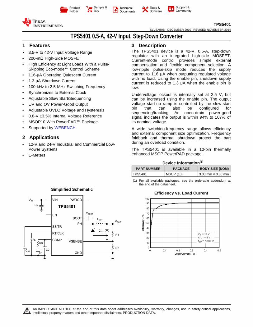
TPS5401 0.5-A, 42-V Input, Step-Down Converter
1
1 Features1• 3.5-V to 42-V Input Voltage Range• 200-mΩ High-Side MOSFET• High Efficiency at Light Loads With a Pulse-
Skipping Eco-mode™ Control Scheme• 116-μA Operating Quiescent Current• 1.3-μA Shutdown Current• 100-kHz to 2.5-MHz Switching Frequency• Synchronizes to External Clock• Adjustable Slow Start/Sequencing• UV and OV Power-Good Output• Adjustable UVLO Voltage and Hysteresis• 0.8-V ±3.5% Internal Voltage Reference• MSOP10 With PowerPAD™ Package• Supported by WEBENCH
2 Applications• 12-V and 24-V Industrial and Commercial Low-
Power Systems• E-Meters
3 DescriptionThe TPS5401 device is a 42-V, 0.5-A, step-downregulator with an integrated high-side MOSFET.Current-mode control provides simple externalcompensation and flexible component selection. Alow-ripple pulse-skip mode reduces the supplycurrent to 116 μA when outputting regulated voltagewith no load. Using the enable pin, shutdown supplycurrent is reduced to 1.3 μA when the enable pin islow.
Undervoltage lockout is internally set at 2.5 V, butcan be increased using the enable pin. The outputvoltage start-up ramp is controlled by the slow-startpin that can also be configured forsequencing/tracking. An open-drain power-goodsignal indicates the output is within 94% to 107% ofits nominal voltage.
A wide switching-frequency range allows efficiencyand external component size optimization. Frequencyfoldback and thermal shutdown protect the partduring an overload condition.
The TPS5401 is available in a 10-pin thermallyenhanced MSOP PowerPAD package.
Device Information(1)
PART NUMBER PACKAGE BODY SIZE (NOM)TPS5401 MSOP (10) 3.00 mm × 3.00 mm
(1) For all available packages, see the orderable addendum atthe end of the datasheet.
Simplified SchematicEfficiency vs. Load Current

2
TPS5401SLVSAB0B –DECEMBER 2010–REVISED NOVEMBER 2014 www.ti.com
Product Folder Links: TPS5401
Submit Documentation Feedback Copyright © 2010–2014, Texas Instruments Incorporated
Table of Contents1 Features .................................................................. 12 Applications ........................................................... 13 Description ............................................................. 14 Revision History..................................................... 25 Pin Configuration and Functions ......................... 36 Specifications......................................................... 4
6.1 Absolute Maximum Ratings ...................................... 46.2 ESD Ratings.............................................................. 46.3 Recommended Operating Conditions....................... 46.4 Thermal Information .................................................. 56.5 Electrical Characteristics........................................... 56.6 Typical Characteristics .............................................. 7
7 Detailed Description ............................................ 117.1 Overview ................................................................. 117.2 Functional Block Diagram ....................................... 127.3 Feature Description................................................. 12
7.4 Device Functional Modes........................................ 238 Application and Implementation ........................ 25
8.1 Application Information............................................ 258.2 Typical Application ................................................. 25
9 Power Supply Recommendations ...................... 3710 Layout................................................................... 37
10.1 Layout Guidelines ................................................. 3710.2 Layout Example .................................................... 3710.3 Estimated Circuit Area .......................................... 38
11 Device and Documentation Support ................. 3811.1 Device Support...................................................... 3811.2 Documentation Support ........................................ 3811.3 Trademarks ........................................................... 3811.4 Electrostatic Discharge Caution............................ 3811.5 Glossary ................................................................ 38
12 Mechanical, Packaging, and OrderableInformation ........................................................... 38
4 Revision HistoryNOTE: Page numbers for previous revisions may differ from page numbers in the current version.
Changes from Revision A (December 2010) to Revision B Page
• Deleted SWIFT™ from the data sheet title............................................................................................................................. 1• Deleted Features: "For SWIFT™ Power Products Documentation, see http://www.ti.com/swift ........................................... 1• Moved the Storage temperature range to the Absolute Maximum Ratings ........................................................................... 4• Changed the Handling Ratings table To: ESD Ratings ......................................................................................................... 4
Changes from Original (December 2010) to Revision A Page
• Added, updated, or renamed the following sections: Device Information Table, Application and Implementation;Power Supply Recommendations; Layout; Device and Documentation Support; Mechanical, Packaging, andOrdering Information .............................................................................................................................................................. 1

1
2
3
4
5 6
7
9
8
10
Thermal Pad(11)
BOOT
VIN
EN
PH
GND
COMP
VSENSE
PWRGD
SS/TR
RT/CLK
3
TPS5401www.ti.com SLVSAB0B –DECEMBER 2010–REVISED NOVEMBER 2014
Product Folder Links: TPS5401
Submit Documentation FeedbackCopyright © 2010–2014, Texas Instruments Incorporated
5 Pin Configuration and Functions
DGQ Package10-Pin MSOP with PowerPAD™
Top View
Pin FunctionsPIN
I/O DESCRIPTIONNAME NO.
BOOT 1 O A bootstrap capacitor is required between BOOT and PH. If the voltage on this capacitor is below theminimum required by the output device, the output is forced to switch off until the capacitor is refreshed.
COMP 8 O Error amplifier output, and input to the output switch current comparator. Connect frequency compensationcomponents to this pin.
EN 3 I Enable pin, internal pullup current source. Pull below 1.2 V to disable. Float to enable. Adjust the inputundervoltage lockout with two resistors.
GND 9 – GroundPH 10 O The source of the internal high-side power MOSFET
PWRGD 6 O An open-drain output; asserts low if output voltage is low due to thermal shutdown, dropout, overvoltage orEN shutdown.
RT/CLK 5 I
Resistor timing and external clock. An internal amplifier holds this pin at a fixed voltage when using anexternal resistor to ground to set the switching frequency. If the pin is pulled above the PLL upper threshold,a mode change occurs and the pin becomes a synchronization input. The internal amplifier is disabled andthe pin is a high-impedance clock input to the internal PLL. If clocking edges stop, the internal amplifier is re-enabled and the mode returns to a resistor-set function.
SS/TR 4 I Slow-start and tracking. An external capacitor connected to this pin sets the output rise time. Because thevoltage on this pin overrides the internal reference, it can be used for tracking and sequencing.
VIN 2 I Input supply voltage, 3.5 V to 42 V.VSENSE 7 I Inverting node of the transconductance (gm) error amplifier.Thermal pad (11) – GND pin must be electrically connected to the thermal pad on the printed circuit board for proper operation.
4
TPS5401SLVSAB0B –DECEMBER 2010–REVISED NOVEMBER 2014 www.ti.com
Product Folder Links: TPS5401
Submit Documentation Feedback Copyright © 2010–2014, Texas Instruments Incorporated
(1) Stresses beyond those listed under Absolute Maximum Ratings may cause permanent damage to the device. These are stress ratingsonly, and functional operation of the device at these or any other conditions beyond those indicated under Recommended OperatingConditions is not implied. Exposure to absolute-maximum-rated conditions for extended periods may affect device reliability.
6 Specifications
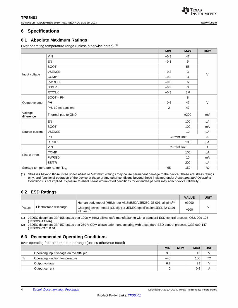
6.1 Absolute Maximum RatingsOver operating temperature range (unless otherwise noted). (1)
MIN MAX UNIT
Input voltage
VIN –0.3 47
V
EN –0.3 5BOOT 55VSENSE –0.3 3COMP –0.3 3PWRGD –0.3 6SS/TR –0.3 3RT/CLK –0.3 3.6
Output voltageBOOT – PH 8
VPH –0.6 47PH, 10-ns transient –2 47
Voltagedifference Thermal pad to GND ±200 mV
Source current
EN 100 μABOOT 100 mAVSENSE 10 μAPH Current limit ART/CLK 100 μA
Sink current
VIN Current limit ACOMP 100 μAPWRGD 10 mASS/TR 200 μA
Storage temperature range, Tstg –65 150 °C
(1) JEDEC document JEP155 states that 1000-V HBM allows safe manufacturing with a standard ESD control process. QSS 009-105(JESD22-A114A)
(2) JEDEC document JEP157 states that 250-V CDM allows safe manufacturing with a standard ESD control process. QSS 009-147(JESD22-C101B.01)
6.2 ESD RatingsVALUE UNIT
V(ESD) Electrostatic dischargeHuman body model (HBM), per ANSI/ESDA/JEDEC JS-001, all pins (1) ±1000
VCharged device model (CDM), per JEDEC specification JESD22-C101,all pins (2) ÷500
6.3 Recommended Operating Conditionsover operating free-air temperature range (unless otherwise noted)
MIN NOM MAX UNITOperating input voltage on the VIN pin 3.5 42 V
TJ Operating junction temperature –40 150 °COutput voltage 0.8 39 VOutput current 0 0.5 A

5
TPS5401www.ti.com SLVSAB0B –DECEMBER 2010–REVISED NOVEMBER 2014
Product Folder Links: TPS5401
Submit Documentation FeedbackCopyright © 2010–2014, Texas Instruments Incorporated
(1) For more information about traditional and new thermal metrics, see the Semiconductor and IC Package Thermal Metrics applicationreport (SPRA953).
6.4 Thermal Information
THERMAL METRIC (1) DGQUNIT
10 PINSRθJA Junction-to-ambient thermal resistance 65.0
°C/W
RθJC(top) Junction-to-case(top) thermal resistance 48.0RθJB Junction-to-board thermal resistance 38.2ψJT Junction-to-top characterization parameter 2.0ψJB Junction-to-board characterization parameter 37.9RθJC(bot) Junction-to-case(bottom) thermal resistance 13.6
6.5 Electrical CharacteristicsTJ = –40°C to 150°C, VIN = 3.5 V to 42 V (unless otherwise noted)
PARAMETER TEST CONDITIONS MIN TYP MAX UNITSUPPLY VOLTAGE (VIN PIN)VIN Operating input voltage 3.5 42 V
Internal undervoltage lockoutthreshold No voltage hysteresis, rising and falling 2.5 V
Shutdown supply current VEN = 0 V 1.3 4μAOperating: nonswitching supply
current VVSENSE = 0.83 V, VIN = 12 V, 25°C 116 136
ENABLE AND UVLO (EN PIN)Enable threshold voltage No voltage hysteresis, rising and falling, 25°C 0.9 1.25 1.55 V
Input currentEnable threshold 50 mV –3.8
μAEnable threshold –50 mV –0.9
Hysteresis current –2.9 μAVOLTAGE REFERENCEVref Voltage reference 0.772 0.8 0.828 VHIGH-SIDE MOSFET
On-resistanceVIN = 3.5 V, VBOOT – VPH = 3 V 300
mΩVIN = 12 V, VBOOT – VPH = 6 V 200 410
ERROR AMPLIFIERInput current 50 nA
gmEA
Error amplifier transconductance –2 μA < ICOMP < 2 μA, VCOMP = 1 V 97 μMhos
Error amplifier transconductanceduring slow-start
–2 μA < ICOMP < 2 μA, VCOMP = 1 V,VVSENSE = 0.4 V 26 μMhos
Error amplifier dc gain VVSENSE = 0.8 V 10,000 V/VError amplifier bandwidth 2700 kHzError amplifier source/sink VCOMP = 1 V, 100 mV overdrive ±7 μA
gmPSCOMP to switch currenttransconductance 1.9 A/V
CURRENT LIMITCurrent limit threshold VIN = 12 V, TJ = 25°C 0.6 0.94 A
THERMAL SHUTDOWNThermal shutdown 182 °C

6
TPS5401SLVSAB0B –DECEMBER 2010–REVISED NOVEMBER 2014 www.ti.com
Product Folder Links: TPS5401
Submit Documentation Feedback Copyright © 2010–2014, Texas Instruments Incorporated
Electrical Characteristics (continued)TJ = –40°C to 150°C, VIN = 3.5 V to 42 V (unless otherwise noted)
PARAMETER TEST CONDITIONS MIN TYP MAX UNITTIMING RESISTOR AND EXTERNAL CLOCK (RT/CLK PIN)
Switching-frequency range using RTmode 100 2500 kHz
fSW Switching frequency RT = 200 kΩ 450 581 720 kHzSwitching-frequency range usingCLK mode 300 2200 kHz
Minimum CLK input pulse width 40 nsRT/CLK high threshold 1.9 2.2 VRT/CLK low threshold 0.5 0.7 VRT/CLK falling edge to PH risingedge delay Measured at 500 kHz with RT resistor in series 60 ns
PLL lock-in time Measured at 500 kHz 100 μsSLOW-START AND TRACKING (SS/TR PIN)
Charge current VSS/TR = 0.4 V 2 μASS/TR-to-VSENSE matching VSS/TR = 0.4 V 45 mVSS/TR-to-reference crossover 98% nominal 1 VSS/TR discharge current (overload) VSENSE = 0 V, VSS/TR = 0.4 V 112 μASS/TR discharge voltage VVSENSE = 0 V 54 mV
POWER GOOD (PWRGD PIN)
VSENSE low thresholdVVSENSE falling 92%
VrefVVSENSE rising 94%
VSENSE high thresholdVVSENSE rising 109%
VrefVVSENSE falling 107%Hysteresis VVSENSE falling 2%Output-high leakage VVSENSE = Vref, VPWRGD = 5.5 V, 25°C 10 nAOn-resistance IPWRGD = 3 mA, VVSENSE < 0.77 V 50 ΩMinimum VIN for defined output VPWRGD < 0.5 V, IPWRGD = 100 μA 0.95 1.5 V

0
500
1000
1500
2000
2500
0 25 50 75 100 125 150 175 200
RT/CLK – Clock Setting Resistance – kW
f–
Sw
itc
hin
g F
req
ue
nc
y–
kH
zS
W
V = 12 V
T = 25°C
IN
J
0
100
200
300
400
500
200 300 400 500 600 700 800 900 1000 1100
RT/CLK – Clock Setting Resistance – kW
f–
Sw
itc
hin
g F
req
ue
nc
y–
kH
zS
W
1200
V = 12 V
T = 25°C
IN
J
0.7
0.8
0.9
1.1
–50 –25 0 25 50 75 100 125 150
Sw
itch
Cu
rre
nt
–A
T – Junction Temperature – °CJ
1
V = 12 VIN
550
570
580
590
600
610
–50 –25 0 25 50 75 100 125 150
f–
Sw
itc
hin
g F
req
ue
nc
y–
kH
zS
W
560
T – Junction Temperature – °CJ
V = 12 V
R = 200 k
IN
TW
0
125
250
375
500
–50 –25 0 25 50 75 100 125 150
T – Junction Temperature – °CJ
r–
Sta
tic
Dra
in-S
ou
rce
On
-Sta
te R
es
ista
nc
e–
mD
S(o
n)
W
V – V = 3 VBOOT PH
V – VBOOT PH
= 6 V
V = 12 VIN
0.784
0.792
0.800
0.808
0.816
–50 –25 0 25 50 75 100 125 150
V–
Vo
lta
ge
Re
fere
nc
e–
Vre
f
T – Junction Temperature – °CJ
V = 12 VIN
7
TPS5401www.ti.com SLVSAB0B –DECEMBER 2010–REVISED NOVEMBER 2014
Product Folder Links: TPS5401
Submit Documentation FeedbackCopyright © 2010–2014, Texas Instruments Incorporated
6.6 Typical Characteristics
Figure 1. On-resistance vs Junction Temperature Figure 2. Voltage Reference vs Junction Temperature
Figure 3. Switch-current Limit vs Junction Temperature Figure 4. Switching Frequency vs Junction Temperature
Figure 5. Switching Frequency vs RT/CLK Resistance High-frequency Range
Figure 6. Switching Frequency vs RT/CLK Resistance Low-frequency Range

–3
–2.5
–2
–1.5
–1
–50 –25 0 25 50 75 100 125 150
I–
SS
/TR
Pin
Ch
arg
e C
urr
en
tA
SS
/TR
m–
T – Junction Temperature °CJ –
V = 12 VIN
–1
–0.95
–0.9
–0.85
–0.8
–50 –25 0 25 50 75 100 125 150
I–
EN
Pin
Cu
rre
nt
AE
Nm
–
T Junction Temperature °CJ – –
V = 12 V
V = Threshold 50 mV
IN
EN–
–4.25
–4
–3.75
–3.5
–3.25
–50 –25 0 25 50 75 100 125 150
I–
EN
Pin
Cu
rre
nt
AE
Nm
–
T Junction Temperature °CJ – –
V = 12 V
V = Threshold + 50 mV
IN
EN
1.1
1.2
1.3
1.4
–50 –25 0 25 50 75 100 125 150
En
ab
le T
hre
sh
old
Vo
lta
ge
–V
T – Junction Temperature – °CJ
V = 12 VIN
50
70
90
110
130
150
–50 –25 0 25 50 75 100 125 150
gm
–E
ATra
ns
co
nd
uc
tan
ce
–A
/Vm
T – Junction Temperature – °CJ
V = 12 VIN
10
20
30
40
–50 –25 0 25 50 75 100 125 150
gm
–E
ATra
ns
co
nd
uc
tan
ce
–A
/Vm
T – Junction Temperature – °CJ
V = 12 VIN
8
TPS5401SLVSAB0B –DECEMBER 2010–REVISED NOVEMBER 2014 www.ti.com
Product Folder Links: TPS5401
Submit Documentation Feedback Copyright © 2010–2014, Texas Instruments Incorporated
Typical Characteristics (continued)
Figure 7. EA Transconductance During Slow-start vsJunction Temperature
Figure 8. EA Transconductance vs Junction Temperature
Figure 9. Enable Threshold Voltage vs JunctionTemperature
Figure 10. EN Pin Current vs Junction Temperature
Figure 11. EN Pin Current vs Junction Temperature Figure 12. SS/TR Charge Current vs Junction Temperature
90
100
110
120
130
140
–50 –25 0 25 50 75 100 125 150
I–
VIN
Su
pp
ly C
urr
en
t–
AV
INm
T – Junction Temperature – °CJ
V = 12 V
V = 0.83 V
IN
VSENSE
90
100
110
120
130
140
0 20 40
I–
VIN
Su
pp
ly C
urr
en
t–
AV
INm
V – Input Voltage – VIN
T = 25 C,
V = 0.83 VJ
VSENSE
o
0
0.5
1
1.5
2
0 10 20 30 40
V – Input Voltage – VIN
I–
Sh
utd
ow
n S
up
ply
Cu
rre
nt
–A
VIN
m
T = 25°CJ
0
0.5
1
1.5
2
–50 –25 0 25 50 75 100 125 150
I–
Sh
utd
ow
n S
up
ply
Cu
rre
nt
–A
VIN
m
T – Junction Temperature – °CJ
V = 12 VIN
0
20
40
60
80
100
0 0.2 0.4 0.6 0.8
V –VSENSE Voltage at VSENSE Pin – V
V = 12 V
T = 25°C
IN
J
% o
f N
om
ina
l f s
w
100
105
110
115
120
–50 –25 0 25 50 75 100 125 150
I–
SS
/TR
Pin
Dis
ch
arg
e C
urr
en
t–
AS
S/T
Rm
T – Junction Temperature – °CJ
V = 12 VIN
9
TPS5401www.ti.com SLVSAB0B –DECEMBER 2010–REVISED NOVEMBER 2014
Product Folder Links: TPS5401
Submit Documentation FeedbackCopyright © 2010–2014, Texas Instruments Incorporated
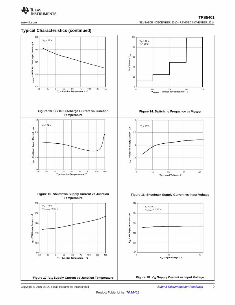
Typical Characteristics (continued)
Figure 13. SS/TR Discharge Current vs JunctionTemperature
Figure 14. Switching Frequency vs VSENSE
Figure 15. Shutdown Supply Current vs JunctionTemperature
Figure 16. Shutdown Supply Current vs Input Voltage
Figure 17. VIN Supply Current vs Junction Temperature Figure 18. VIN Supply Current vs Input Voltage

0
100
200
300
400
500
0 200 400 600 800 1000
V – mVVSENSE
Off
se
t–
mV
V = 12 VIN
T = 25 CJ
o
600
30
35
40
45
50
55
60
–50 –25 0 25 50 75 100 125 150
Off
se
t–
mV
V = 0.2 VSS/TR
V = 12 VIN
T – Junction Temperature – °CJ
1.5
1.8
2
2.3
2.5
–50 –25 0 25 50 75 100 125 150
BO
OT
to
PH
UV
LO
Th
res
ho
ld V
olt
ag
e–
V
T – Junction Temperature – °CJ
2
2.25
2.5
2.75
3
–50 –25 0 25 50 75 100 125 150
Inp
ut
Vo
lta
ge
UV
LO
–V
T – Junction Temperature – °CJ
85
90
95
100
105
110
115
–50 –25 0 25 50 75 100 125 150
PW
RG
D T
hre
sh
old
–%
of
Vre
f
V FallingVSENSE
V RisingVSENSE
V FallingVSENSE
V RisingVSENSE
V = 12 VIN
T – Junction Temperature – °CJ
0
20
40
60
80
100
–50 –25 0 25 50 75 100 125 150
r–
DS
(on)
W
T – Junction Temperature – °CJ
V = 12 VIN
10
TPS5401SLVSAB0B –DECEMBER 2010–REVISED NOVEMBER 2014 www.ti.com
Product Folder Links: TPS5401
Submit Documentation Feedback Copyright © 2010–2014, Texas Instruments Incorporated
Typical Characteristics (continued)
Figure 19. PWRGD On-resistance vs Junction Temperature Figure 20. PWRGD Threshold vs Junction Temperature
Figure 21. Boot to PH UVLO Threshold vs JunctionTemperature
Figure 22. Input Voltage UVLO vs Junction Temperature
Figure 23. SS/TR to VSENSE Offset vs VSENSE Voltage Figure 24. SS/TR to VSENSE Offset vs Temperature

11
TPS5401www.ti.com SLVSAB0B –DECEMBER 2010–REVISED NOVEMBER 2014
Product Folder Links: TPS5401
Submit Documentation FeedbackCopyright © 2010–2014, Texas Instruments Incorporated
7 Detailed Description
7.1 OverviewThe TPS5401 device is a 42-V, 0.5-A, step-down (buck) regulator with an integrated high-side n-channelMOSFET. To improve performance during line and load transients, the device implements a constant-frequency,current-mode control which reduces output capacitance and simplifies external frequency compensation design.The wide switching-frequency range of 100 kHz to 2500 kHz allows for efficiency and size optimization whenselecting the output filter components. The switching frequency is adjusted using a resistor to ground on theRT/CLK pin. The device has an internal phase-lock loop (PLL) on the RT/CLK pin that is used to synchronize thepower-switch turnon to a falling edge of an external system clock.
The TPS5401 device has a default start-up voltage of approximately 2.5 V. The EN pin has an internal pullupcurrent source that can be used to adjust the input voltage undervoltage lockout (UVLO) threshold with twoexternal resistors. In addition, the pullup current provides a default condition. When the EN pin is floating, thedevice operates. The operating current is 116 μA when not switching and under no load. When the device isdisabled, the supply current is 1.3 μA.
The integrated 200-mΩ high-side MOSFET allows for high-efficiency power-supply designs capable of delivering0.5 amperes of continuous current to a load. The TPS5401 reduces the external component count by integratingthe boot recharge diode. The bias voltage for the integrated high-side MOSFET is supplied by a capacitor fromthe BOOT pin to the PH pin. The boot capacitor voltage is monitored by a UVLO circuit and turns the high-sideMOSFET off when the boot voltage falls below a preset threshold. The TPS5401 can operate at high duty cyclesbecause of the boot UVLO. The output voltage can be stepped down to as low as the 0.8-V reference.
The TPS5401 has a power-good comparator (PWRGD) which asserts when the regulated output voltage is lessthan 92% or greater than 109% of the nominal output voltage. The PWRGD pin is an open-drain output whichdeasserts when the VSENSE pin voltage is between 94% and 107% of the nominal output voltage, allowing thepin to transition high when a pullup resistor is used.
The TPS5401 minimizes excessive output overvoltage (OV) transients by taking advantage of the OV power-good comparator. When the OV comparator is activated, the high-side MOSFET is turned off and masked fromturning on until the output voltage is lower than 107%.
The SS/TR (slow-start/tracking) pin is used to minimize inrush currents or provide power-supply sequencingduring power up. A small-value capacitor should be coupled to the pin to adjust the slow-start time. A resistordivider can be coupled to the pin for critical power-supply sequencing requirements. The SS/TR pin is dischargedbefore the output powers up. This discharging ensures a repeatable restart after an overtemperature fault, UVLOfault, or a disabled condition.
The TPS5401 also discharges the slow-start capacitor during overload conditions with an overload recoverycircuit. The overload recovery circuit slow-starts the output from the fault voltage to the nominal regulationvoltage once a fault condition is removed. A frequency-foldback circuit reduces the switching frequency duringstart-up and overcurrent fault conditions to help control the inductor current.

ERROR
AMPLIFIER
Boot
Charge
Boot
UVLO
UVLO
Current
Sense
Oscillator
with PLL
Frequency
Shift
Logic
And
PWM Latch
Slope
Compensation
PWM
Comparator
Minimum
Clamp
Pulse
Skip
Maximum
Clamp
Voltage
Reference
Overload
Recovery
VSENSE
SS/TR
COMP
RT/CLK
PH
BOOT
VIN
Thermal
Shutdown
EN
Enable
Comparator
Shutdown
Logic
Shutdown
Enable
Threshold
TPS5401 Block Diagram
Logic
Shutdown
PWRGD
Shutdown
OV
GND
Thermal
Pad
7
4
8
5
9
11
10
1
236
UV
12
TPS5401SLVSAB0B –DECEMBER 2010–REVISED NOVEMBER 2014 www.ti.com
Product Folder Links: TPS5401
Submit Documentation Feedback Copyright © 2010–2014, Texas Instruments Incorporated
7.2 Functional Block Diagram
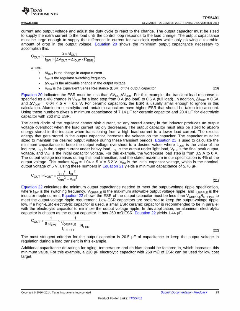
7.3 Feature Description
7.3.1 Fixed Frequency PWM ControlThe TPS5401 uses an adjustable fixed-frequency, peak current mode control. The output voltage is comparedthrough external resistors on the VSENSE pin to an internal voltage reference by an error amplifier which drivesthe COMP pin. An internal oscillator initiates the turnon of the high-side power switch. The error amplifier outputis compared to the high-side power-switch current. When the power-switch current reaches the level set by theCOMP voltage, the power switch is turned off. The COMP pin voltage increases and decreases as the outputcurrent increases and decreases. The device implements a current limit by clamping the COMP pin voltage to amaximum level. The Eco-mode control scheme is implemented with a minimum clamp on the COMP pin.
7.3.2 Slope Compensation Output CurrentThe TPS5401 adds a compensating ramp to the switch current signal. This slope compensation prevents sub-harmonic oscillations. The available peak inductor current remains constant over the full duty-cycle range.

V–
Inp
ut
Vo
lta
ge
–V
IN
I – Output Current – AOUT
V = 3.3 VOUT
4.6
4.8
5
5.2
5.4
5.6
0 0.05 0.10 0.15 0.20
I – Output Current – AOUT
V–
Inp
ut
Vo
lta
ge
–V
IN
V = 5 VOUT
Start
Stop
13
TPS5401www.ti.com SLVSAB0B –DECEMBER 2010–REVISED NOVEMBER 2014
Product Folder Links: TPS5401
Submit Documentation FeedbackCopyright © 2010–2014, Texas Instruments Incorporated
Feature Description (continued)7.3.3 Low-Dropout Operation and Bootstrap Voltage (BOOT)The TPS5401 has an integrated boot regulator, and requires a small ceramic capacitor between the BOOT andPH pins to provide the gate-drive voltage for the high-side MOSFET. The BOOT capacitor is refreshed when thehigh-side MOSFET is off and the low-side diode conducts. The value of this ceramic capacitor should be 0.1 μF.A ceramic capacitor with an X7R or X5R grade dielectric with a voltage rating of 10 V or higher is recommendedbecause of the stable characteristics over temperature and voltage.
To improve dropout, the TPS5401 device is designed to operate at 100% duty cycle as long as the BOOT-to-PHpin voltage is greater than 2.1 V. When the voltage from BOOT to PH drops below 2.1 V, the high-side MOSFETis turned off using an UVLO circuit, which allows the low-side diode to conduct and refresh the charge on theBOOT capacitor. Because the supply current sourced from the BOOT capacitor is low, the high-side MOSFETcan remain on for more switching cycles than are required to refresh the capacitor. Therefore, the effective dutycycle of the switching regulator is high.
The effective duty cycle during dropout of the regulator is mainly influenced by the voltage drops across thepower MOSFET, inductor resistance, low-side diode, and printed circuit board resistance. During operatingconditions in which the input voltage drops and the regulator is operating in continuous conduction mode, thehigh-side MOSFET can remain on for 100% of the duty cycle to maintain output regulation, until the BOOT-to-PHvoltage falls below 2.1 V.
Attention must be taken in maximum-duty-cycle applications which experience extended time periods with lightloads or no load. When the voltage across the BOOT capacitor falls below the 2.1-V UVLO threshold, the high-side MOSFET is turned off, but there may not be enough inductor current to pull the PH pin down to recharge theBOOT capacitor. The high-side MOSFET of the regulator stops switching because the voltage across the BOOTcapacitor is less than 2.1 V. The output capacitor then decays until the difference in the input voltage and outputvoltage is greater than 2.1 V, at which point the BOOT UVLO threshold is exceeded, and the device startsswitching again until the desired output voltage is reached. This operating condition persists until the inputvoltage and/or the load current increases. It is recommended to adjust the VIN stop voltage greater than theBOOT UVLO trigger condition at the minimum load of the application using the adjustable VIN UVLO feature withresistors on the EN pin.
The start and stop voltages for typical 3.3-V and 5-V output applications are shown in Figure 25 and Figure 26.The voltages are plotted versus load current. The start voltage is defined as the input voltage needed to regulatethe output voltage within 3.5%. The stop voltage is defined as the input voltage at which the output drops by 5%or stops switching.
During high-duty-cycle conditions, the inductor current ripple increases while the BOOT capacitor is beingrecharged, resulting in an increase in ripple voltage on the output. This is due to the recharge time of the bootcapacitor being longer than the typical high-side off time, when switching occurs every cycle.
Figure 25. 3.3-V Start/Stop Voltage Figure 26. 5-V Start/Stop Voltage

ENA
START ENA1
VR2
V VI
R1
=
-
+
START STOP
HYS
V VR1
I
-
=
EN
VIN
+
–
TPS5401
R1
R2
IHYS
I
0.9 A
1
m
1.25 V
2.9 Am
OUTV 0.8 VR1 = R2
0.8 V
-æ ö´ ç ÷
è ø
14
TPS5401SLVSAB0B –DECEMBER 2010–REVISED NOVEMBER 2014 www.ti.com
Product Folder Links: TPS5401
Submit Documentation Feedback Copyright © 2010–2014, Texas Instruments Incorporated
Feature Description (continued)7.3.4 Error AmplifierThe TPS5401 has a transconductance amplifier as the error amplifier. The error amplifier compares the VSENSEvoltage to the lower of the SS/TR pin voltage or the internal 0.8-V voltage reference. The transconductance (gm)of the error amplifier is 97 μA/V during normal operation. During the slow-start operation, the transconductance isa fraction of the normal operating gm. When the voltage of the VSENSE pin is below 0.8 V and the device isregulating using the SS/TR voltage, the gm is 26 μA/V.
The frequency compensation components (series resistor and capacitor) are connected between the COMP pinand ground.
7.3.5 Voltage ReferenceThe voltage reference system produces a precise ±3.5% voltage reference over temperature by scaling theoutput of a temperature-stable bandgap circuit.
7.3.6 Adjusting the Output VoltageThe output voltage is set with a resistor divider from the output node to the VSENSE pin. It is recommended touse 1% tolerance or better divider resistors. Start with 10 kΩ for the R2 resistor and use Equation 1 to calculateR1. To improve efficiency at light loads, consider using larger-value resistors. If the values are too high, theregulator becomes more susceptible to noise, and voltage errors from the VSENSE input current becomenoticeable.
(1)
7.3.7 Enabling and Adjusting Undervoltage LockoutThe TPS5401 is disabled when the VIN pin voltage falls below 2.5 V. If an application requires a higherundervoltage lockout (UVLO), use the EN pin as shown in Figure 27 to adjust the input voltage UVLO by usingthe two external resistors. Though it is not necessary to use the UVLO adjust resistors, for operation it is highlyrecommended to provide consistent power-up behavior. The EN pin has an internal pullup current source, I1, of0.9 μA that provides the default condition of the TPS5401 operating when the EN pin floats. Once the EN pinvoltage exceeds the enable threshold voltage (VENA) of 1.25 V, an additional 2.9 μA of hysteresis, IHYS, is added.This additional current facilitates input-voltage hysteresis. Use Equation 2 to calculate R1 which sets the externalhysteresis for the input voltage. Use Equation 3 to calculate R2 which sets the input start voltage.
Figure 27. Adjustable Undervoltage Lockout (UVLO)
(2)
(3)

VEN
VSS/TR
VVSENSE
VOUT
ss ssss
ref
t (ms) I ( A)C (nF) =
V (V) 0.8
m´
´
15
TPS5401www.ti.com SLVSAB0B –DECEMBER 2010–REVISED NOVEMBER 2014
Product Folder Links: TPS5401
Submit Documentation FeedbackCopyright © 2010–2014, Texas Instruments Incorporated
Feature Description (continued)7.3.8 Slow-Start/Tracking Pin (SS/TR)The TPS5401 effectively uses the lower voltage of the internal voltage reference or the SS/TR pin voltage as thepower-supply reference voltage and regulates the output accordingly. A capacitor on the SS/TR pin to groundimplements a slow-start time. The TPS5401 has an internal pullup current source of 2 μA that charges theexternal slow-start capacitor. The calculations for the slow-start time (10% to 90%) are shown in Equation 4. Thevoltage reference (Vref) is 0.8 V and the slow-start current (ISS) is 2 μA. The slow-start capacitor should remainlower than 0.47 μF and greater than 0.47 nF.
(4)
At power up, the TPS5401 does not start switching until the slow-start pin is discharged to less than 40 mV toensure a proper power up; see Figure 28.
Also, during normal operation, the TPS5401 stops switching and SS/TR must be discharged to 40 mV when theVIN UVLO is exceeded, the EN pin is pulled below 1.25 V, or a thermal shutdown event occurs.
The VSENSE voltage follows the SS/TR pin voltage with a 45-mV offset up to 85% of the internal voltagereference. When the SS/TR voltage is greater than 85% of the internal reference voltage, the offset increases asthe effective system reference transitions from the SS/TR voltage to the internal voltage reference (seeFigure 23). The SS/TR voltage ramps linearly until clamped at 1.7 V.
Figure 28. Operation of SS/TR Pin When Starting
7.3.9 Overload Recovery CircuitThe TPS5401 has an overload recovery (OLR) circuit. The OLR circuit slow-starts the output from the overloadvoltage to the nominal regulation voltage once the fault condition is removed. The OLR circuit discharges theSS/TR pin to a voltage slightly greater than the VSENSE pin voltage, using an internal pulldown of 100 μA whenthe error amplifier is changed to a high voltage from a fault condition. When the fault condition is removed, theoutput slow-starts from the fault voltage to nominal output voltage.

VEN1
VPWRGD1
VOUT1
VOUT2
SS /TR
TPS5401
EN
PWRGD
SS/TR
ENPWRGD
16
TPS5401SLVSAB0B –DECEMBER 2010–REVISED NOVEMBER 2014 www.ti.com
Product Folder Links: TPS5401
Submit Documentation Feedback Copyright © 2010–2014, Texas Instruments Incorporated
Feature Description (continued)7.3.10 SequencingMany of the common power-supply sequencing methods can be implemented using the SS/TR, EN and PWRGDpins. The sequential method can be implemented using an open-drain output of a power-on-reset pin of anotherdevice. The sequential method is illustrated in Figure 29 using two TPS5401 devices. The power good is coupledto the EN pin on the TPS5401, which enables the second power supply once the primary supply reachesregulation. If needed, a 1-nF ceramic capacitor on the EN pin of the second power supply provides a 1-ms start-up delay. Figure 30 shows the results of Figure 29.
Figure 29. Schematic for Sequential Start-Up Sequence
Figure 30. Sequential Start-Up Using EN and PWRGD
V , VEN1 EN2
VOUT1
VOUT2
EN
TPS54160
3
SS/TR4
PWRGD6
EN
TPS54160
3
SS/TR4
PWRGD6
TPS5401
TPS5401
17
TPS5401www.ti.com SLVSAB0B –DECEMBER 2010–REVISED NOVEMBER 2014
Product Folder Links: TPS5401
Submit Documentation FeedbackCopyright © 2010–2014, Texas Instruments Incorporated
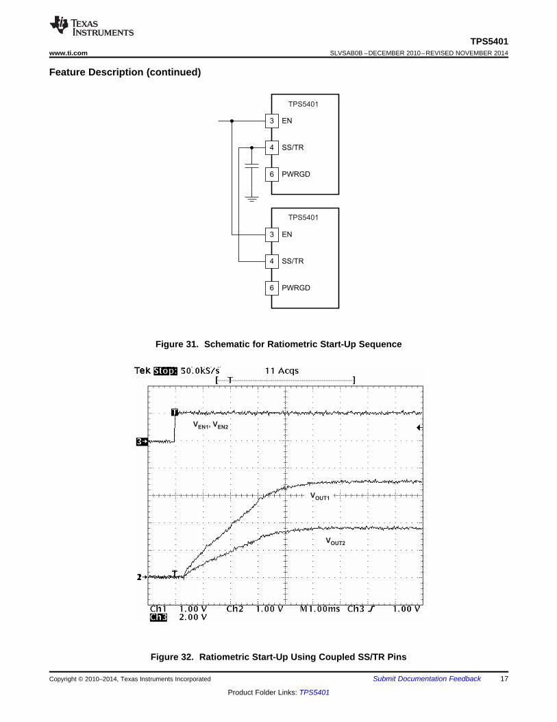
Feature Description (continued)
Figure 31. Schematic for Ratiometric Start-Up Sequence
Figure 32. Ratiometric Start-Up Using Coupled SS/TR Pins
SS /TR
TPS5401
EN
PWRGD
SS / TR
EN
VSENSE
VOUT1
VOUT2
R1
R2
R3
R4
TPS5401
PWRGD
18
TPS5401SLVSAB0B –DECEMBER 2010–REVISED NOVEMBER 2014 www.ti.com
Product Folder Links: TPS5401
Submit Documentation Feedback Copyright © 2010–2014, Texas Instruments Incorporated
Feature Description (continued)Figure 31 shows a method for ratiometric start-up sequence by connecting the SS/TR pins together. Theregulator outputs ramp up and reach regulation at the same time. When calculating the slow-start time, the pullupcurrent source must be doubled in Equation 4. Figure 32 shows the results of Figure 31.
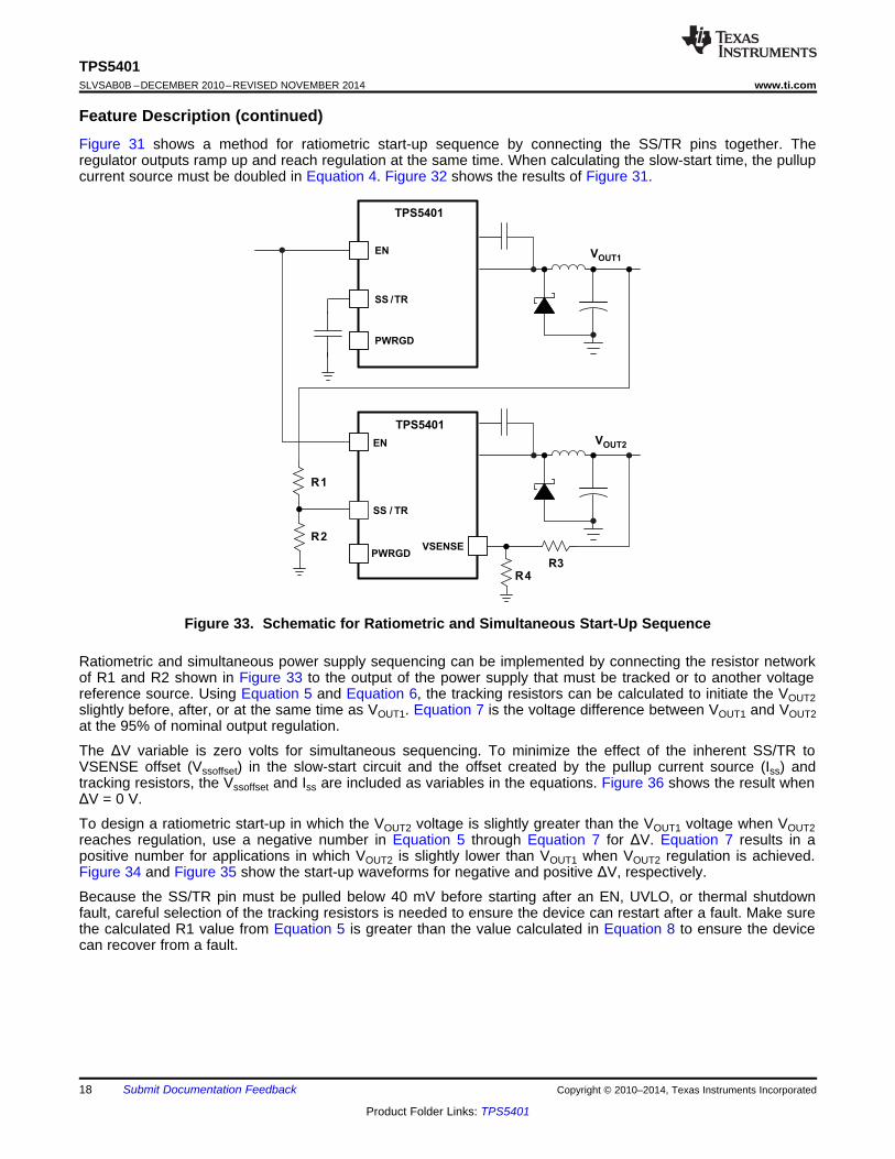
Figure 33. Schematic for Ratiometric and Simultaneous Start-Up Sequence
Ratiometric and simultaneous power supply sequencing can be implemented by connecting the resistor networkof R1 and R2 shown in Figure 33 to the output of the power supply that must be tracked or to another voltagereference source. Using Equation 5 and Equation 6, the tracking resistors can be calculated to initiate the VOUT2slightly before, after, or at the same time as VOUT1. Equation 7 is the voltage difference between VOUT1 and VOUT2at the 95% of nominal output regulation.
The ΔV variable is zero volts for simultaneous sequencing. To minimize the effect of the inherent SS/TR toVSENSE offset (Vssoffset) in the slow-start circuit and the offset created by the pullup current source (Iss) andtracking resistors, the Vssoffset and Iss are included as variables in the equations. Figure 36 shows the result whenΔV = 0 V.
To design a ratiometric start-up in which the VOUT2 voltage is slightly greater than the VOUT1 voltage when VOUT2reaches regulation, use a negative number in Equation 5 through Equation 7 for ΔV. Equation 7 results in apositive number for applications in which VOUT2 is slightly lower than VOUT1 when VOUT2 regulation is achieved.Figure 34 and Figure 35 show the start-up waveforms for negative and positive ΔV, respectively.
Because the SS/TR pin must be pulled below 40 mV before starting after an EN, UVLO, or thermal shutdownfault, careful selection of the tracking resistors is needed to ensure the device can restart after a fault. Make surethe calculated R1 value from Equation 5 is greater than the value calculated in Equation 8 to ensure the devicecan recover from a fault.

VEN
VOUT1
VOUT2
VEN
VOUT1
VOUT2
VEN
VOUT1
VOUT2
OUT1R1 2800 V 180 V> ´ - ´ D
OUT1 OUT2V V VD = -
ref
OUT2 ref
V R1R2 =
V + V V
´
D -
OUT2 ssoffset
ref ss
V + V VR1 = ×
V I
D
19
TPS5401www.ti.com SLVSAB0B –DECEMBER 2010–REVISED NOVEMBER 2014
Product Folder Links: TPS5401
Submit Documentation FeedbackCopyright © 2010–2014, Texas Instruments Incorporated
Feature Description (continued)As the SS/TR voltage becomes more than 85% of the nominal reference voltage, the Vssoffset becomes larger asthe slow-start circuits gradually hand off the regulation reference to the internal voltage reference. The SS/TR pinvoltage must be greater than 1.3 V for a complete handoff to the internal voltage reference as shown inFigure 23.
(5)
(6)
(7)
(8)
Figure 34. Ratiometric Start-Up With VOUT2 Leading VOUT1 Figure 35. Ratiometric Start-Up With VOUT1 Leading VOUT2
Figure 36. Simultaneous Start-Up

T 1.0888SW
206,003R (kΩ)
f (kHz)=
20
TPS5401SLVSAB0B –DECEMBER 2010–REVISED NOVEMBER 2014 www.ti.com
Product Folder Links: TPS5401
Submit Documentation Feedback Copyright © 2010–2014, Texas Instruments Incorporated
Feature Description (continued)7.3.11 Constant Switching Frequency and Timing Resistor (RT/CLK Pin)The switching frequency of the TPS5401 is adjustable over a wide range from approximately 100 kHz to 2500kHz by placing a resistor on the RT/CLK pin. The RT/CLK pin voltage is typically 0.5 V and must have a resistorto ground to set the switching frequency. To determine the timing resistance for a given switching frequency, useEquation 9 or the curves in Figure 5 or Figure 6. To reduce the solution size one would typically set the switchingfrequency as high as possible, but tradeoffs of the supply efficiency, maximum input voltage, and minimumcontrollable on-time should be considered.
The minimum controllable on-time is typically 130 ns and limits the maximum operating input voltage.
The maximum switching frequency is also limited by the frequency-shift circuit. More discussion on the details ofthe maximum switching frequency is located as follows.
(9)
7.3.12 Overcurrent Protection and Frequency ShiftThe TPS5401 implements current-mode control, which uses the COMP pin voltage to turn off the high-sideMOSFET on a cycle-by-cycle basis. Each cycle, the switch current and COMP pin voltage are compared. Whenthe peak switch current intersects the COMP voltage, the high-side switch is turned off. During overcurrentconditions that pull the output voltage low, the error amplifier responds by driving the COMP pin high, increasingthe switch current. The error amplifier output is clamped internally, which functions as a switch-current limit.
To increase the maximum operating switching frequency at high input voltages, the TPS5401 implements afrequency shift. The switching frequency is divided by 8, 4, 2, and 1 as the voltage ramps from 0 to 0.8 volts onthe VSENSE pin.
The device implements a digital frequency shift to enable synchronizing to an external clock during normal start-up and fault conditions. Because the device can only divide the switching frequency by 8, there is a maximuminput voltage limit in which the device operates and still has frequency-shift protection.
During short-circuit events (particularly with high-input-voltage applications), the control loop has a finite minimumcontrollable on-time, and the output has a low voltage. During the switch on-time, the inductor current ramps tothe peak current limit because of the high input voltage and minimum on-time. During the switch off-time, theinductor current would normally not have enough off-time and output voltage to ramp down by the ramp-upamount. The frequency shift effectively increases the off-time, allowing the current to ramp down.
7.3.13 Selecting the Switching FrequencyThe switching frequency that is selected should be the lower value of the two equations, Equation 10 andEquation 11. Use Equation 10 to calculate the maximum switching frequency limitation set by the minimumcontrollable on-time. Setting the switching frequency above this value causes the regulator to skip switchingpulses.
Equation 11 is the maximum switching frequency limit set by the frequency-shift protection. To have adequateoutput short-circuit protection at high input voltages, the switching frequency should be set to be less than thefSW(maxshift) frequency. Equation 11. To calculate the maximum switching frequency in Equation 11, account forthe output voltage decrease from the nominal voltage to 0 volts and the fDIV integer increase from 1 to 8, whichcorresponds to the frequency shift.

10 20 30 40
2500
2000
1500
1000
500
0
f–
Sw
itch
ing
Fre
qu
en
cy
–kH
zS
W
V – Input Voltage – VIN
V = 5 VOUT
Shift
Skip
DIV L dc OUT(sc) dSWshift
on(min) IN L DS(on) d
I R V V
t V I R V
æ ö´ + += ´ ç ÷
ç ÷- ´ +è ø
ff
( )( )
L dc OUT dSW max skip
on(min) IN L dDS on
I R V V1
t V I R V
æ ö´ + +ç ÷= ´ç ÷- ´ +è ø
f
21
TPS5401www.ti.com SLVSAB0B –DECEMBER 2010–REVISED NOVEMBER 2014
Product Folder Links: TPS5401
Submit Documentation FeedbackCopyright © 2010–2014, Texas Instruments Incorporated
Feature Description (continued)In Figure 37, the solid line illustrates a typical safe operating area regarding frequency shift and assumes anoutput voltage of zero volts, an inductor resistance of 0.13 Ω, FET on-resistance of 0.2 Ω, and a diode voltagedrop of 0.5 V. The dashed line is the maximum switching frequency to avoid pulse skipping. Enter theseequations in a spreadsheet or other software or use the WEBENCH design software to determine the switchingfrequency.
where• ton(min) is the minimum controllable on-time• IL is the inductor current• Rdc is the inductor resistance• Vdis the diode voltage drop• VIN is the maximum input voltage• VOUT is the output voltage• RDS(on) is the switch-on resistance (10)
where• ƒDIV is the frequency divide, which equals 1, 2, 4, or 8• VOUT(sc) is the output voltage during short (11)
Figure 37. Maximum Switching Frequency vs. Input Voltage
7.3.14 How to Interface to RT/CLK PinThe RT/CLK pin can be used to synchronize the regulator to an external system clock. To implement thesynchronization feature, connect a square wave to the RT/CLK pin as shown in Figure 38. The square-waveamplitude must transition lower than 0.5 V and higher than 2.2 V on the RT/CLK pin and have an on-time greaterthan 40 ns and an off-time greater than 40 ns. The synchronization frequency range is 300 kHz to 2200 kHz. Therising edge of the PH signal is synchronized to the falling edge of the RT/CLK pin signal.
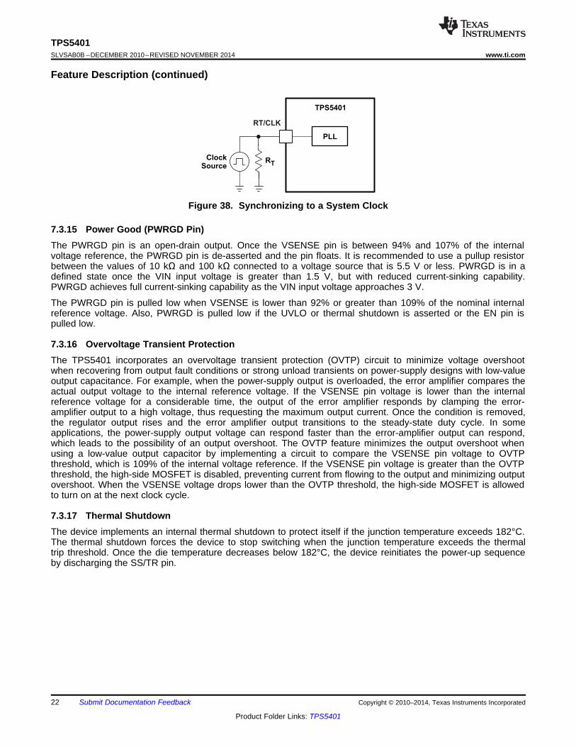
TPS5401
Clock
Source
PLL
RT
RT/CLK
22
TPS5401SLVSAB0B –DECEMBER 2010–REVISED NOVEMBER 2014 www.ti.com
Product Folder Links: TPS5401
Submit Documentation Feedback Copyright © 2010–2014, Texas Instruments Incorporated
Feature Description (continued)
Figure 38. Synchronizing to a System Clock
7.3.15 Power Good (PWRGD Pin)The PWRGD pin is an open-drain output. Once the VSENSE pin is between 94% and 107% of the internalvoltage reference, the PWRGD pin is de-asserted and the pin floats. It is recommended to use a pullup resistorbetween the values of 10 kΩ and 100 kΩ connected to a voltage source that is 5.5 V or less. PWRGD is in adefined state once the VIN input voltage is greater than 1.5 V, but with reduced current-sinking capability.PWRGD achieves full current-sinking capability as the VIN input voltage approaches 3 V.
The PWRGD pin is pulled low when VSENSE is lower than 92% or greater than 109% of the nominal internalreference voltage. Also, PWRGD is pulled low if the UVLO or thermal shutdown is asserted or the EN pin ispulled low.
7.3.16 Overvoltage Transient ProtectionThe TPS5401 incorporates an overvoltage transient protection (OVTP) circuit to minimize voltage overshootwhen recovering from output fault conditions or strong unload transients on power-supply designs with low-valueoutput capacitance. For example, when the power-supply output is overloaded, the error amplifier compares theactual output voltage to the internal reference voltage. If the VSENSE pin voltage is lower than the internalreference voltage for a considerable time, the output of the error amplifier responds by clamping the error-amplifier output to a high voltage, thus requesting the maximum output current. Once the condition is removed,the regulator output rises and the error amplifier output transitions to the steady-state duty cycle. In someapplications, the power-supply output voltage can respond faster than the error-amplifier output can respond,which leads to the possibility of an output overshoot. The OVTP feature minimizes the output overshoot whenusing a low-value output capacitor by implementing a circuit to compare the VSENSE pin voltage to OVTPthreshold, which is 109% of the internal voltage reference. If the VSENSE pin voltage is greater than the OVTPthreshold, the high-side MOSFET is disabled, preventing current from flowing to the output and minimizing outputovershoot. When the VSENSE voltage drops lower than the OVTP threshold, the high-side MOSFET is allowedto turn on at the next clock cycle.
7.3.17 Thermal ShutdownThe device implements an internal thermal shutdown to protect itself if the junction temperature exceeds 182°C.The thermal shutdown forces the device to stop switching when the junction temperature exceeds the thermaltrip threshold. Once the die temperature decreases below 182°C, the device reinitiates the power-up sequenceby discharging the SS/TR pin.

23
TPS5401www.ti.com SLVSAB0B –DECEMBER 2010–REVISED NOVEMBER 2014
Product Folder Links: TPS5401
Submit Documentation FeedbackCopyright © 2010–2014, Texas Instruments Incorporated
Feature Description (continued)
(1) Refer to Simplified Schematic.
7.3.18 Current-Mode Compensation DesignTo simplify design efforts using the TPS5401, the typical designs for common applications are listed in Table 1.For designs using ceramic output capacitors, TI recommends proper derating of ceramic output capacitancewhen conducting the stability analysis because the actual ceramic capacitance drops considerably from thenominal value when the applied voltage increases. Advanced users may see the Detailed Design Procedure infor detailed guidelines or use the WEBENCH tool.
Table 1. Typical Designs (1)
VIN(V)
VOUT(V)
fSW(kHz)
LOUT(µH) COUT
R1(kΩ)
R2(kΩ)
C2(pF)
C1(pF)
R3(kΩ)
7.5 V–35 V 5 700 47 Aluminum, 220 µF/260 mΩ 52.3 10 82 3300 6987.5 V–35 V 5 700 47 Ceramic, 47 µF/10V 52.3 10 5.6 3300 7512 V–42 V 5 700 47 Aluminum, 100 µF/300 mΩ 52.3 10 100 3300 31612 V–42 V 3.3 700 33 Ceramic, 33 µF/10 V 30.9 10 10 3300 478 V–14 V 5 700 33 Ceramic, 47 µF/10 V 52.3 10 5.6 3300 75
7.4 Device Functional Modes
7.4.1 Pulse-Skip Eco-mode Control SchemeThe TPS5401 operates in a pulse-skip Eco-mode control scheme at light load currents to improve efficiency byreducing switching and gate-drive losses. The TPS5401 is designed so that if the output voltage is withinregulation and the peak switch current at the end of any switching cycle is below the pulse-skipping currentthreshold, the device enters the Eco-mode control scheme. This current threshold is the current levelcorresponding to a nominal COMP voltage of 500 mV.
When in the Eco-mode control scheme, the COMP pin voltage is clamped at 500 mV, and the high-sideMOSFET is inhibited. Further decreases in load current or increases in output voltage cannot drive the COMPpin below this clamp voltage level.
Because the device is not switching, the output voltage begins to decay. As the voltage control loopcompensates for the falling output voltage, the COMP pin voltage begins to rise. At this time, the high-sideMOSFET is enabled, and a switching pulse initiates on the next switching cycle. The peak current is set by theCOMP pin voltage. The output voltage recharges the regulated value (see Figure 39); then the peak switchcurrent starts to decrease and eventually falls below the Eco-mode control-scheme threshold, at which time thedevice again enters the Eco-mode control scheme.
For Eco-mode control-scheme operation, the TPS5401 senses peak current, not average or load current, so theload current where the device enters the Eco-mode control scheme is dependent on the output inductor value.For example, the circuit in Figure 40 enters the Eco-mode control scheme at about 20 mA of output current.When the load current is low and the output voltage is within regulation, the device enters a sleep mode anddraws only 116 μA of input quiescent current. The internal PLL remains operating when in sleep mode. Whenoperating at light load currents in the pulse-skip mode, the switching transitions occur synchronously with theexternal clock signal.

V acOUT
IL
VPH
24
TPS5401SLVSAB0B –DECEMBER 2010–REVISED NOVEMBER 2014 www.ti.com
Product Folder Links: TPS5401
Submit Documentation Feedback Copyright © 2010–2014, Texas Instruments Incorporated
Device Functional Modes (continued)
Figure 39. Pulse-Skip Mode Operation

+
25
TPS5401www.ti.com SLVSAB0B –DECEMBER 2010–REVISED NOVEMBER 2014
Product Folder Links: TPS5401
Submit Documentation FeedbackCopyright © 2010–2014, Texas Instruments Incorporated
8 Application and Implementation
NOTEInformation in the following applications sections is not part of the TI componentspecification, and TI does not warrant its accuracy or completeness. TI’s customers areresponsible for determining suitability of components for their purposes. Customers shouldvalidate and test their design implementation to confirm system functionality.
8.1 Application InformationThe TPS5401 is good for the E-meter application. The power supply design is a challenge work to E-meterdesigners because it must get enough output current from a wide input voltage range with a limited input power.For example, in China, a single-phase or three-phase E-meter must work properly with an input AC electricityvoltage range from 0.7 Un to 1.9 Un. Here Un is the phase voltage of 220 V. The input active power limit is 1.5W. A typical power supply design uses a transformer followed by a rectifier bridge to get a low unregulated dcvoltage. Then a voltage regulator generates 5 V for the whole system. Considering the ac transformer has largeinternal dc resistance and the following rectifier has a voltage drop, the output voltage of the rectifier circuit isdifferent between empty load and heavy load. So the input voltage for the voltage regulator within the whole acinput voltage range may have a maximum-to-minimum ratio of 4. In this situation, a linear regulator is not suitabledue to its very low efficiency at high input voltage.
8.2 Typical Application
Figure 40. Typical Application Schematic

1æ ö
-ç ÷è ø
OUT
ref
VR6 = x R7
V
26
TPS5401SLVSAB0B –DECEMBER 2010–REVISED NOVEMBER 2014 www.ti.com
Product Folder Links: TPS5401
Submit Documentation Feedback Copyright © 2010–2014, Texas Instruments Incorporated
Typical Application (continued)8.2.1 Design RequirementsFigure 40 shows a typical TPS5401 application schematic for this requirement. The input range is set to 7.5 V to35 V. With such a wide input voltage range, an inexpensive transformer with high dc resistance can be used tosave total cost.
8.2.2 Detailed Design ProcedureThe following design procedure can be used to select component values for the TPS5401. Alternately, theWEBENCH software may be used to generate a complete design. The WEBENCH software uses an iterativedesign procedure and accesses a comprehensive database of components when generating a design. Thissection presents a simplified discussion of the design process. To begin the design process, a few parametersmust be decided upon. Table 2 lists the parameters the designer needs to know.
Table 2. Design ParametersDESIGN PARAMETER EXAMPLE VALUE
Input voltage range 7.5 V to 35 VOutput voltage 5 V
Input ripple voltage 300 mVOutput ripple voltage 1% of VOUT
Output transient response for 0 to 500-mA load step 4% of VOUT
Maximum output current 500 mA
8.2.2.1 Switching FrequencyThe first step is to decide on a switching frequency for the regulator. Typically, the user may want to choose thehighest switching frequency possible, because this produces the smallest solution size. The high switchingfrequency allows for lower-valued inductors and smaller output capacitors compared to a power supply thatswitches at a lower frequency. Alternatively, the user may choose a lower switching frequency to improveefficiency. At lower switching frequencies, switching losses are minimized. The switching frequency that can beselected is limited by the minimum on-time of the internal power switch, the input voltage, the output voltage, andthe frequency shift limitation.
Equation 10 and Equation 11 must be used to find the maximum switching frequency for the regulator. Choosethe lower value of the two equations. Switching frequencies higher than these values result in pulse skipping orthe lack of overcurrent protection during a short circuit.
The typical minimum on-time, ton(min), is 130 ns for the TPS5401. For this example, the output voltage is 5 V andthe maximum input voltage is 35 V, which allows for a maximum switch frequency up to 1213 kHz when includingthe inductor resistance, on-resistance, and diode voltage in Equation 10. To ensure overcurrent runaway is not aconcern during short circuits in your design, use Equation 11 or the solid curve in Figure 37 to determine themaximum switching frequency. With a maximum input voltage of 35 V, assuming a diode voltage of 0.5 V,inductor resistance of 130 mΩ, switch resistance of 400 mΩ, a current-limit value of 0.94 A, and a short-circuitoutput voltage of 0.1 V, the maximum switching frequency is approximately 1265 kHz. Choosing high frequencycan reduce external component size but results in higher switching loss. To achieve a balanced design, aswitching frequency of 700 kHz is used. To determine the timing resistance for a given switching frequency, useEquation 9 to get a nearest standard resistance of 165 kΩ. The switching frequency is set to 698 kHz by theresistor R3 shown in Figure 40.
8.2.2.2 Output Voltage SetpointThe output voltage of the TPS5401 is externally adjustable using a resistor divider network. In the applicationcircuit of Figure 40, this divider network is comprised of R6 and R7. The relationship of the output voltage to theresistor divider is given by Equation 12:
(12)
Choosing R7 = 10 kΩ, R6 is calculated to be 52.3 kΩ for an output voltage of 5 V.

OUT(max)INRIPPLE
IN SW
I × 0.25V =
C × f
( )IN OUTOUTINRMS OUT
IN IN
V -VVI = I × ×
V V
27
TPS5401www.ti.com SLVSAB0B –DECEMBER 2010–REVISED NOVEMBER 2014
Product Folder Links: TPS5401
Submit Documentation FeedbackCopyright © 2010–2014, Texas Instruments Incorporated
Due to current leakage of the VSENSE pin, the current flowing through the feedback network should be greaterthan 1 μA in order to maintain the output voltage accuracy. This requirement makes the maximum value of R7equal to 800 kΩ. Choosing higher resistor values decreases quiescent current and improve efficiency at lowoutput currents but may introduce noise immunity problems.
8.2.2.3 Input CapacitorThe TPS5401 requires a high-quality ceramic, type X5R or X7R, input decoupling capacitor with at least 3 μF ofeffective capacitance, and in some applications additional bulk capacitance. The effective capacitance includesany dc bias effects. The voltage rating of the input capacitor must be greater than the maximum input voltage.The capacitor must also have a ripple-current rating greater than the maximum input-current ripple of theTPS5401. Use Equation 13 to calculate the input voltage ripple.
The value of a ceramic capacitor varies significantly over temperature and the amount of dc bias applied to thecapacitor. The capacitance variations due to temperature can be minimized by selecting a dielectric material thatis stable over temperature. X5R and X7R ceramic dielectrics are usually selected for power regulator capacitorsbecause they have a high capacitance-to-volume ratio and are fairly stable over temperature. The outputcapacitor must also be selected with the dc bias taken into account. The capacitance value of a capacitordecreases as the dc bias across a capacitor increases.
For this example design, a ceramic capacitor with at least a 60-V voltage rating is required to support themaximum input voltage. Common standard ceramic capacitor voltage ratings include 4 V, 6.3 V, 10 V, 16 V, 25V, 50 V, and 100 V, so a 100-V capacitor should be selected. For this example, two 2.2-μF, 100-V capacitors inparallel have been selected. Table 3 shows a selection of high-voltage capacitors. The input capacitance valuedetermines the input ripple voltage of the regulator. The input voltage ripple can be calculated using Equation 14.
Using the design example values, IOUT(max) = 0.5 A, CIN = 4.4 μF,and fSW = 700 kHz, yields an input voltage rippleof 40.6 mV and a maximum rms input ripple current of 0.25 A when VIN is equal to 10 V, which is 2 times theoutput voltage of 5 V.
(13)
(14)
Table 3. Capacitor TypesVENDOR VALUE (μF) EIA Size VOLTAGE DIELECTRIC COMMENTS
Murata
1 to 2.21210
100 V
X7R
GRM32 series1 to 4.7 50 V
11206
100 VGRM31 series
1 to 2.2 50 V
Vishay
1 to 1.82220
50 V
VJ X7R series1 to 1.2 100 V1 to 3.9
222550 V
1 to 1.8 100 V
TDK
1 to 2.21812
100 VC series C4532
1.5 to 6.8 50 V1. to 2.2
1210100 V
C series C32251 to 3.3 50 V
AVX
1 to 4.71210
50 V
X7R dielectric series1 100 V
1 to 4.71812
50 V1 to 2.2 100 V

RIPPLEL(peak) OUT
II I
2= +
( )2
( )2 IN(max) OUT OUTL(RMS) OUT
IN(max) OUT SW
V V V1I I
12 V L f
æ ö- ´= + ´ç ÷ç ÷´ ´è ø
( )IN(max) OUT OUTLRIPPLE
IN(max) OUT SW
V V VI
V L f
- ´
=
´ ´
IN(min) OUT OUTOUT(max)
IN(min) SW
V V VL
30mA V f
-
= ´
´
IN(max) OUT OUTOUT(min)
OUT IND IN(max) SW
V V VL
I K V f
-
= ´
´ ´
28
TPS5401SLVSAB0B –DECEMBER 2010–REVISED NOVEMBER 2014 www.ti.com
Product Folder Links: TPS5401
Submit Documentation Feedback Copyright © 2010–2014, Texas Instruments Incorporated
8.2.2.4 Output Inductor SelectionTo calculate the minimum value of the output inductor, use Equation 15.
(15)
KIND is a coefficient that represents the amount of inductor ripple current relative to the maximum output current.
The inductor ripple current is filtered by the output capacitor. Therefore, choosing high inductor ripple currentsimpacts the selection of the output capacitor, because the output capacitor must have a ripple-current ratingequal to or greater than the inductor ripple current. In general, the inductor ripple value is at the discretion of thedesigner. However, the following guidelines may be used.
For designs using low-ESR output capacitors such as ceramics, a value as high as KIND = 0.4 may be used.When using higher-ESR output capacitors, KIND = 0.2 yields better results. Because the inductor ripple current ispart of the PWM control system, the TPS5401 requires ripple current that is always greater than 30 mA fordependable operation. In a wide-input voltage regulator, it is best to choose an inductor ripple current on thelarger side. This allows the inductor to still have a measurable ripple current with the input voltage at itsminimum. The maximum value of the input inductance is limited by Equation 16.
(16)
For this design example, use KIND = 0.3, and the minimum inductor value is calculated to be 42 μH. The neareststandard value was chosen: 47 μH. For the output-filter inductor, it is important that the root-mean-square (rms)current and saturation current ratings not be exceeded. The rms and peak inductor current can be found fromEquation 17 to Equation 19.
(17)
(18)
(19)
As the equation set demonstrates, lower ripple currents reduce the output voltage ripple of the regulator butrequire a larger value of inductance. Selecting higher ripple currents increases the output voltage ripple of theregulator but allows for a lower inductance value. The current flowing through the inductor is the inductor ripplecurrent plus the output current. During power up, faults or transient load conditions, the inductor current canincrease above the calculated peak inductor current level. In transient conditions, the inductor current canincrease up to the switch current limit of the device. For this reason, the most conservative approach is to specifyan inductor with a saturation current rating equal to or greater than the switch current limit rather than the peakinductor current. For this design, ILRIPPLE = 0.1303 A, IL(RMS) = 0.501 A and IL(peak) = 0.565 A. The inductor used isa Coilcraft MSS1048-473ML type, with a saturation current rating of 1.44 A and an rms current rating of 1.83 A.
8.2.2.5 Output CapacitorThere are three primary considerations for selecting the value of the output capacitor. The output capacitordetermines the modulator pole, the output voltage ripple, and how the regulator responds to a large change inload current. The output capacitance must be selected based on the most stringent of these three criteria.
The desired response to a large change in the load current is the first criterion. The output capacitor must supplythe load with current when the regulator cannot. This situation occurs if there are desired hold-up times for theregulator where the output capacitor must hold the output voltage above a certain level for a specified amount oftime after the input power is removed. The regulator also is temporarily unable to supply sufficient output currentif there is a large, fast increase in the current needs of the load, such as when transitioning from no load to a fullload. The regulator usually requires two or more clock cycles for the control loop to detect the change in load
OUTORIPPLESW
ESR
LRIPPLE
1 1C
V8 fR
I
> ´
´-
-
> ´
-
2 2
OH OLOUT OUT 2 2
FIN INI
I IC L
V V
( )OUT
OUT
SW OUT OUT ESR
2 IC
f V I R
´ D>
´ D - D ´
29
TPS5401www.ti.com SLVSAB0B –DECEMBER 2010–REVISED NOVEMBER 2014
Product Folder Links: TPS5401
Submit Documentation FeedbackCopyright © 2010–2014, Texas Instruments Incorporated
current and output voltage and adjust the duty cycle to react to the change. The output capacitor must be sizedto supply the extra current to the load until the control loop responds to the load change. The output capacitancemust be large enough to supply the difference in current for two clock cycles while only allowing a tolerableamount of drop in the output voltage. Equation 20 shows the minimum output capacitance necessary toaccomplish this.
where• ΔIOUT is the change in output current• fSW is the regulator switching frequency• ΔVOUT is the allowable change in the output voltage• RESR is the Equivalent Series Resistance (ESR) of the output capacitor (20)
Equation 20 indicates the ESR must be less than ΔVOUT/ΔIOUT. For this example, the transient load response isspecified as a 4% change in VOUT for a load step from 0 A (no load) to 0.5 A (full load). In addition, ΔIOUT = 0.5Aand ΔVOUT = 0.04 × 5 V = 0.2 V. For ceramic capacitors, the ESR is usually small enough to ignore in thiscalculation. Aluminum electrolytic and tantalum capacitors have higher ESR that should be taken into account.Using these numbers gives a minimum capacitance of 7.14 μF for ceramic capacitor and 20.4 µF for electrolyticcapacitor with 260 mΩ ESR.
The catch diode of the regulator cannot sink current, so any stored energy in the inductor produces an outputvoltage overshoot when the load current rapidly decreases. The output capacitor must also be sized to absorbenergy stored in the inductor when transitioning from a high load current to a lower load current. The excessenergy that gets stored in the output capacitor increases the voltage on the capacitor. The capacitor must besized to maintain the desired output voltage during these transient periods. Equation 21 is used to calculate theminimum capacitance to keep the output voltage overshoot to a desired value, where LOUT is the value of theinductor, IOH is the output current under heavy load, IOL is the output under light load, VFIN is the final peak outputvoltage, and VINI is the initial capacitor voltage. For this example, the worst-case load step is from 0.5 A to 0 A.The output voltage increases during this load transition, and the stated maximum in our specification is 4% of theoutput voltage. This makes VFIN = 1.04 × 5 V = 5.2 V. VINI is the initial capacitor voltage, which is the nominaloutput voltage of 5 V. Using these numbers in Equation 21 yields a minimum capacitance of 5.76 μF.
(21)
Equation 22 calculates the minimum output capacitance needed to meet the output-voltage ripple specification,where fSW is the switching frequency, VORIPPLE is the maximum allowable output voltage ripple, and ILRIPPLE is theinductor ripple current. Equation 22 shows the ESR of the output capacitor must be less than VORIPPLE/ILRIPPLE tomeet the output-voltage ripple requirement. Low-ESR capacitors are preferred to keep the output-voltage ripplelow. If a high-ESR electrolytic capacitor is used, a small ESR ceramic capacitor is recommended to be in parallelwith the electrolytic capacitor to minimize the output voltage ripple. In this application, an aluminum electrolyticcapacitor is chosen as the output capacitor. It has 260 mΩ ESR. Equation 22 yields 1.44 µF.
(22)
The most stringent criterion for the output capacitor is 20.5 µF of capacitance to keep the output voltage inregulation during a load transient in this example.
Additional capacitance de-ratings for aging, temperature and dc bias should be factored in, which increases thisminimum value. For this example, a 220 µF electrolytic capacitor with 260 mΩ of ESR can be used for low costtarget.

( ) ( )2
2
IN(max) OUT OUT FD J SW IN(max) FD
DIN(max)
V V I V C f V VP
V
- ´ ´ ´ ´ += +
( )OUT IN(max) OUT
CO(RMS)
IN(max) OUT SW
V V VI
12 V L f
´ -=
´ ´ ´
30
TPS5401SLVSAB0B –DECEMBER 2010–REVISED NOVEMBER 2014 www.ti.com
Product Folder Links: TPS5401
Submit Documentation Feedback Copyright © 2010–2014, Texas Instruments Incorporated
Capacitors generally have limits to the amount of ripple current they can handle without failing or producingexcess heat. An output capacitor that can support the inductor ripple current must be specified. Some capacitordata sheets specify the root-mean-square (rms) value of the maximum ripple current. Equation 23 can be used tocalculate the rms ripple current the output capacitor must support. For this application, Equation 23 yields 37.6mA.
(23)
8.2.2.6 Catch DiodeThe TPS5401 requires an external catch diode between the PH pin and GND. The selected diode must have areverse voltage rating equal to or greater than VIN(MAX). The peak current rating of the diode must be greater thanthe maximum inductor current. The diode should also have a low forward voltage. Schottky diodes are typically agood choice for the catch diode, due to their low forward voltage. The lower the forward voltage of the diode, thehigher the efficiency of the regulator.
Typically, when the voltage and current ratings for the diode are higher, then the forward voltage is higher.Because the design example has an input voltage up to 42 V, a diode with a minimum of 42-V reverse voltage isselected.
For the example design, the B160A Schottky diode is selected for its lower forward voltage, and it comes in alarger package size which has good thermal characteristics over small devices. The typical forward voltage of theB160A is 0.5 V.
The diode must also be selected with an appropriate power rating. The diode conducts the output current duringthe off-time of the internal power switch. The off-time of the internal switch is a function of the maximum inputvoltage, the output voltage, and the switching frequency. The output current during the off-time is multiplied bythe forward voltage of the diode, which equals the conduction losses of the diode. At higher switch frequencies,the ac losses of the diode must be taken into account. The ac losses of the diode are due to the charging anddischarging of the junction capacitance and reverse recovery. Equation 24 is used to calculate the total powerdissipation, conduction losses plus ac losses, of the diode.
The B160A has a junction capacitance (CJ) of 110 pF. Using Equation 24, the selected diode dissipates 0.29 W.This power dissipation, depending on mounting techniques, should produce a 5.9°C temperature rise in the diodewhen the input voltage is 42 V and the load current is 0.5 A.
If the power supply spends a significant amount of time at light load currents or in sleep mode, consider using adiode which has a low leakage current and slightly higher forward voltage drop.
(24)
8.2.2.7 Slow-Start CapacitorThe slow-start capacitor determines the minimum amount of time it takes for the output voltage to reach itsnominal programmed value during power up. This is useful if a load requires a controlled voltage-slew rate. Thisis also used if the output capacitance is large and would require large amounts of current to quickly charge thecapacitor to the output voltage level. The large currents necessary to charge the capacitor may make theTPS5401 reach the current limit, whereas excessive current draw from the input power supply may cause theinput voltage rail to sag. Limiting the output voltage-slew rate solves both of these problems.

Zmod
ESR OUT
1f
2 R Cp
=
´ ´
OUTPmod
OUT OUT
If
2 V Cp
=
´ ´
OUT OUTSS
SSAVG
C V 0.8t
I
´ ´
>
31
TPS5401www.ti.com SLVSAB0B –DECEMBER 2010–REVISED NOVEMBER 2014
Product Folder Links: TPS5401
Submit Documentation FeedbackCopyright © 2010–2014, Texas Instruments Incorporated
The slow-start time must be long enough to allow the regulator to charge the output capacitor up to the outputvoltage without drawing excessive current. Equation 25 can be used to find the minimum slow-start time, tSS,necessary to charge the output capacitor, COUT, from 10% to 90% of the output voltage, VOUT, with an averageslow-start current of ISSAVG. In the example, to charge the 220 μF output capacitor up to 5 V while only allowingthe average input current ISSAVG to be 0.2 A would require a 4.4-ms slow-start time.
(25)
When the slow-start time is known, the slow-start capacitor value can be calculated using Equation 4. For theexample circuit, the slow-start time is set to a value of 3.2 ms, which requires a 0.01-µF capacitor.
8.2.2.8 Bootstrap Capacitor SelectionA 0.1-μF ceramic capacitor must be connected between the BOOT and PH pins for proper operation. It isrecommended to use a ceramic capacitor with X5R or better grade dielectric. The capacitor should have a 10-Vor higher voltage rating.
8.2.2.9 Undervoltage Lockout Set PointThe undervoltage lockout (UVLO) can be adjusted using an external voltage divider on the EN pin of theTPS5401. The UVLO has two thresholds, one for power up when the input voltage is rising and one for powerdown or brownouts when the input voltage is falling. The supply should turn on and start switching once the inputvoltage increases above power-up threshold (enabled). After the regulator starts switching, it should continue todo so until the input voltage falls below the power-down threshold (UVLO stop).
The programmable UVLO and enable voltages are set using a resistor divider between VIN and ground to the ENpin. Equation 2 through Equation 3 can be used to calculate the resistance values necessary. For the exampleapplication, because the minimum input voltage is 7.5 V, when the maximum input voltage is 35 V, the voltage atthe EN pin exceeds the absolute voltage rating of the EN pin. So the UVLO is not set externally in this design.
8.2.2.10 CompensationThe external compensation used with the TPS5401 allows for a wide range of output filter configurations. A largerange of capacitor values and types of dielectric is supported. This design example uses an aluminum electrolyticoutput capacitor. A design example with the ceramic dielectric output capacitors can be found in the TPS54040data sheet (SLVS918). More accurate designs can be found in the WEBENCH software.
The peak-current mode PWM modulator and the output filter generate a pair of power stage pole and zero whichare determined using Equation 26 and Equation 27.
(26)
(27)
P1
C P
1f
2 R Cp
=
´ ´
Z1
C C
1f
2 R Cp
=
´ ´
DCEA0
EA
AR
gm=
P0
O C
1f
2 R Cp
=
´ ´
refDCEA DCEA
OUT
VG = A ×
V
ROCO
RC
CC
CP
Type2A
COMPVSENSE
VOUT
gmEA
Vref
32
TPS5401SLVSAB0B –DECEMBER 2010–REVISED NOVEMBER 2014 www.ti.com
Product Folder Links: TPS5401
Submit Documentation Feedback Copyright © 2010–2014, Texas Instruments Incorporated
A type 2A compensation scheme is recommended for the TPS5401. As RC, CC, CP shown in Figure 41, thecompensation components are chosen to set the desired loop crossover frequency and phase margin for outputfilter components. The type 2A compensation has the following characteristics: a dc gain, a low-frequency pole,and a mid-frequency zero / pole pair.
Figure 41. The Compensation Recommended for the TPS5401
The dc gain is determined by Equation 28:
where• ADCEA is the error amplifier open-loop dc gain. It is 10,000 V/V. (28)
The low-frequency pole is determined by Equation 29:
where• RO is the output resistance of the error amplifier. It can be calculated by Equation 30. (29)
(30)
The mid-frequency zero is determined by Equation 31.
(31)
Additionally, the mid-frequency pole is given by Equation 32.
(32)
P
Zmod
1C =
2 fp ´
C
Pmod
1C =
2 fp ´
CO OUT OUTC
PS ref EA
2 f C VR = ×
gm V gm
p ´ ´
´
33
TPS5401www.ti.com SLVSAB0B –DECEMBER 2010–REVISED NOVEMBER 2014
Product Folder Links: TPS5401
Submit Documentation FeedbackCopyright © 2010–2014, Texas Instruments Incorporated
The first step is to choose the closed-loop crossover frequency fCO. In general, the closed-loop crossoverfrequency could be less than 1/10 of the minimum operating frequency. For the TPS5401, the maximum closed-loop crossover frequency must not be not greater than 40 kHz. For this example, we choose 15-kHz crossoverfrequency. Next, by definition, the magnitude of the loop gain at the crossover frequency is 0 dB. By placing thecompensation zero at the power stage pole, and the mid-compensation pole at the power stage zero, the RC, CCand CP can be approximately calculated by Equation 33 through Equation 35.
(33)
(34)
where• gmPS is the power-stage transconductance. It is 1.9 A/V• gmEA is the error-amplifier transconductance. It is 97 μA/V (35)
For this design, the calculated values are as follows:• R3 = 37.4 kΩ• C6 = 2200 pF• C7 = 22 pF
8.2.2.11 Discontinuous Mode and Eco-mode Control-Scheme BoundaryWith an input voltage of 34 V, the power supply enters discontinuous mode when the output current is less than50 mA. The power supply enters Eco-mode control scheme when the output current is lower than 30 mA.
A(max) J(max) JA TOTT T Pq= - ´
J A JA TOTT T Pq= - ´
TOT CON SW GD SUPP = P + P + P + P
6
SUP INP = 116 10 V-
´ ´
9
GD IN SWP = V 3 10 f-
´ ´ ´
2 9
sw IN OUT SWP = V l 0.25 10 f-
´ ´ ´ ´
2 OUTcon OUT DS(on)
IN
VP = I r
V´ ´
34
TPS5401SLVSAB0B –DECEMBER 2010–REVISED NOVEMBER 2014 www.ti.com
Product Folder Links: TPS5401
Submit Documentation Feedback Copyright © 2010–2014, Texas Instruments Incorporated
8.2.2.12 Power Dissipation EstimateThe following formulas show how to estimate the IC power dissipation under continuous-conduction mode (CCM)operation. These equations should not be used if the device is working in discontinuous-conduction mode(DCM).
The power dissipation of the IC includes conduction loss (PCON), switching loss (Psw), gate-drive loss (PGD), andsupply current (PSUP).
(36)
(37)
(38)
(39)
Therefore, total power dissipation is:
(40)
For a given ambient temperature TA, the junction temperature TJ can be estimated by Equation 41.
where• RθJA is the thermal resistance of the package (°C/W) (41)
For given TJ(max) = 150°C, the maximum allowed ambient temperature can be estimated by Equation 42.
(42)
There are additional power losses in the regulator circuit due to the inductor ac and dc losses, the catch diodeand trace resistance that impact the overall efficiency of the regulator.

PH = 20 V / div
V = 100 mV / div (ac coupled)IN
Inductor Current = 100 mA / div
Time = 1 µsec / div
PH = 20 V div
V = 20 mV / div (ac coupled)OUT
Inductor Current = 100 mA div
Time = 20 usec / div
PH = 20 V div
V = 20 mV / div (ac coupled)OUT
Inductor Current = 100 mA div
Time = 1 usec / div
PH = 20 V div
V = 20 mV / div (ac coupled)OUT
Inductor Current = 100 mA div
Time = 1 usec / div
V = 50 mV / div (ac coupled)OUT
I = 200 mA / divOUT
Time = 200 µsec / div
V = 20 V / divIN
V = 2 V / divOUT
EN = 2 V / div
Time = 5 msec / div
35
TPS5401www.ti.com SLVSAB0B –DECEMBER 2010–REVISED NOVEMBER 2014
Product Folder Links: TPS5401
Submit Documentation FeedbackCopyright © 2010–2014, Texas Instruments Incorporated
8.2.3 Application Curves
Figure 42. Load Transient (100 mA to 350 mA) Figure 43. Start-Up With Input Voltage
Figure 44. Output Ripple, CCM Figure 45. Output Ripple, DCM
Figure 46. Output Ripple, PSM Figure 47. Input Ripple, CCM

−0.10
−0.08
−0.06
−0.04
−0.02
0.00
0.02
0.04
0.06
0.08
0.10
0 0.1 0.2 0.3 0.4 0.5
Re
gu
latio
n -
%
I - Output Current - AOUT
V = 24 VIN
−0.10
−0.08
−0.06
−0.04
−0.02
0.00
0.02
0.04
0.06
0.08
0.10
5 10 15 20 25 30 35
Re
gu
latio
n -
%
V - Input Voltage - VIN
I = 0.25 AOUT
100 1000 10000 100000 1000000−60
−40
−20
0
20
40
60
−180
−120
−60
0
60
120
180
Gain
- d
B
Phase -
°
Frequency - Hz
Gain
Phase
0
10
20
30
40
50
60
70
80
90
100
0.001 0.01 0.1 1
Effic
ien
cy -
%
I - Output Current - AOUT
V = 35 VIN
V = 24 VIN
V = 15 VIN
V = 7.5 VIN
0
10
20
30
40
50
60
70
80
90
100
0 0.1 0.2 0.3 0.4 0.5
Effic
ien
cy -
%
I - Output Current - AOUT
V = 35 VIN
V = 24 VIN
V = 15 VIN V = 7.5 VIN
PH = 20 V div
V = 100 mV / div (ac coupled)OUT
Inductor Current = 100 mA div
Time = 1 usec / div
36
TPS5401SLVSAB0B –DECEMBER 2010–REVISED NOVEMBER 2014 www.ti.com
Product Folder Links: TPS5401
Submit Documentation Feedback Copyright © 2010–2014, Texas Instruments Incorporated
Figure 48. Input Ripple, DCM Figure 49. Efficiency vs Load Current
Figure 50. Light-Load Efficiency Figure 51. Overall Loop-Frequency Response
Figure 52. Regulation vs Load Current Figure 53. Regulation vs Input Voltage

BOOT
VIN
EN
SS/TR
RT/CLK
PH
GND
COMP
VSENSE
PWRGD
Input
Bypass
Capacitor
UVLO
Adjust
Resistors
Slow Start
CapacitorFrequency
Set Resistor
Compensation
NetworkResistor
Divider
Output
Inductor
Output
Capacitor
Vout
Vin
TopsideGround
AreaCatch
Diode
Route Boot CapacitorTrace on another layer toprovide wide path fortopside ground
Thermal VIA
Signal VIA
37
TPS5401www.ti.com SLVSAB0B –DECEMBER 2010–REVISED NOVEMBER 2014
Product Folder Links: TPS5401
Submit Documentation FeedbackCopyright © 2010–2014, Texas Instruments Incorporated
9 Power Supply RecommendationsThe device is designed to operate from an input-voltage supply range between 3.5 V and 42 V. This input supplyshould be well regulated. If the input supply is located more than a few inches from the converter additional bulkcapacitance may be required in addition to the ceramic bypass capacitors. An electrolytic capacitor with a valueof 100 μF is a typical choice.
10 Layout
10.1 Layout GuidelinesLayout is a critical portion of good power-supply design. There are several signal paths that conduct fast-changing currents or voltages that can interact with stray inductance or parasitic capacitance to generate noiseor degrade the power-supply performance. To help eliminate these problems, the VIN pin should be bypassed toground with a low-ESR ceramic bypass capacitor with X5R or X7R dielectric. Care should be taken to minimizethe loop area formed by the bypass capacitor connections, the VIN pin, and the anode of the catch diode. SeeFigure 54 for a PCB layout example. The GND pin should be tied directly to the thermal pad under the IC.
The thermal pad should be connected to any internal PCB ground planes using multiple vias directly under theIC. The PH pin should be routed to the cathode of the catch diode and to the output inductor. Because the PHconnection is the switching node, the catch diode and output inductor should be located close to the PH pins,and the area of the PCB conductor minimized to prevent excessive capacitive coupling. For operation at full ratedload, the top-side ground area must provide adequate heat dissipating area. The RT/CLK pin is sensitive tonoise, so the RT resistor should be located as close as possible to the IC and routed with minimal lengths oftrace. The additional external components can be placed approximately as shown. It may be possible to obtainacceptable performance with alternate PCB layouts; however, this layout has been shown to produce goodresults and is meant as a guideline.
10.2 Layout Example
Figure 54. PCB Layout Example
38
TPS5401SLVSAB0B –DECEMBER 2010–REVISED NOVEMBER 2014 www.ti.com
Product Folder Links: TPS5401
Submit Documentation Feedback Copyright © 2010–2014, Texas Instruments Incorporated
10.3 Estimated Circuit AreaThe estimated printed circuit board area for the components used in the design of Figure 40 is 0.55 in2 (3.55cm2). This area does not include test points or connectors.
11 Device and Documentation Support
11.1 Device Support
11.1.1 Development Support• WEBENCH
11.1.2 Third-Party Products DisclaimerTI'S PUBLICATION OF INFORMATION REGARDING THIRD-PARTY PRODUCTS OR SERVICES DOES NOTCONSTITUTE AN ENDORSEMENT REGARDING THE SUITABILITY OF SUCH PRODUCTS OR SERVICESOR A WARRANTY, REPRESENTATION OR ENDORSEMENT OF SUCH PRODUCTS OR SERVICES, EITHERALONE OR IN COMBINATION WITH ANY TI PRODUCT OR SERVICE.
11.2 Documentation Support
11.2.1 Related Documentation• Semiconductor and IC Package Thermal Metrics (SPRA953).• TPS54040 0.5-A, 42V Step Down DC/DC Converter with Eco-Mode data sheet (SLVS918).
11.3 TrademarksEco-mode, PowerPAD are trademarks of Texas Instruments.All other trademarks are the property of their respective owners.
11.4 Electrostatic Discharge CautionThese devices have limited built-in ESD protection. The leads should be shorted together or the device placed in conductive foamduring storage or handling to prevent electrostatic damage to the MOS gates.
11.5 GlossarySLYZ022 — TI Glossary.
This glossary lists and explains terms, acronyms, and definitions.
12 Mechanical, Packaging, and Orderable InformationThe following pages include mechanical, packaging, and orderable information. This information is the mostcurrent data available for the designated devices. This data is subject to change without notice and revision ofthis document. For browser-based versions of this data sheet, refer to the left-hand navigation.

PACKAGE OPTION ADDENDUM
www.ti.com 2-Aug-2016
Addendum-Page 1
PACKAGING INFORMATION
Orderable Device Status(1)
Package Type PackageDrawing
Pins PackageQty
Eco Plan(2)
Lead/Ball Finish(6)
MSL Peak Temp(3)
Op Temp (°C) Device Marking(4/5)
Samples
TPS5401DGQ ACTIVE MSOP-PowerPAD
DGQ 10 80 Green (RoHS& no Sb/Br)
CU NIPDAUAG Level-1-260C-UNLIM -40 to 150 5401
TPS5401DGQR ACTIVE MSOP-PowerPAD
DGQ 10 2500 Green (RoHS& no Sb/Br)
CU NIPDAUAG Level-1-260C-UNLIM -40 to 150 5401
TPS5401DGQT ACTIVE MSOP-PowerPAD
DGQ 10 250 Green (RoHS& no Sb/Br)
CU NIPDAUAG Level-1-260C-UNLIM -40 to 150 5401
(1) The marketing status values are defined as follows:ACTIVE: Product device recommended for new designs.LIFEBUY: TI has announced that the device will be discontinued, and a lifetime-buy period is in effect.NRND: Not recommended for new designs. Device is in production to support existing customers, but TI does not recommend using this part in a new design.PREVIEW: Device has been announced but is not in production. Samples may or may not be available.OBSOLETE: TI has discontinued the production of the device.
(2) Eco Plan - The planned eco-friendly classification: Pb-Free (RoHS), Pb-Free (RoHS Exempt), or Green (RoHS & no Sb/Br) - please check http://www.ti.com/productcontent for the latest availabilityinformation and additional product content details.TBD: The Pb-Free/Green conversion plan has not been defined.Pb-Free (RoHS): TI's terms "Lead-Free" or "Pb-Free" mean semiconductor products that are compatible with the current RoHS requirements for all 6 substances, including the requirement thatlead not exceed 0.1% by weight in homogeneous materials. Where designed to be soldered at high temperatures, TI Pb-Free products are suitable for use in specified lead-free processes.Pb-Free (RoHS Exempt): This component has a RoHS exemption for either 1) lead-based flip-chip solder bumps used between the die and package, or 2) lead-based die adhesive used betweenthe die and leadframe. The component is otherwise considered Pb-Free (RoHS compatible) as defined above.Green (RoHS & no Sb/Br): TI defines "Green" to mean Pb-Free (RoHS compatible), and free of Bromine (Br) and Antimony (Sb) based flame retardants (Br or Sb do not exceed 0.1% by weightin homogeneous material)
(3) MSL, Peak Temp. - The Moisture Sensitivity Level rating according to the JEDEC industry standard classifications, and peak solder temperature.
(4) There may be additional marking, which relates to the logo, the lot trace code information, or the environmental category on the device.
(5) Multiple Device Markings will be inside parentheses. Only one Device Marking contained in parentheses and separated by a "~" will appear on a device. If a line is indented then it is a continuationof the previous line and the two combined represent the entire Device Marking for that device.
(6) Lead/Ball Finish - Orderable Devices may have multiple material finish options. Finish options are separated by a vertical ruled line. Lead/Ball Finish values may wrap to two lines if the finishvalue exceeds the maximum column width.
Important Information and Disclaimer:The information provided on this page represents TI's knowledge and belief as of the date that it is provided. TI bases its knowledge and belief on informationprovided by third parties, and makes no representation or warranty as to the accuracy of such information. Efforts are underway to better integrate information from third parties. TI has taken and

PACKAGE OPTION ADDENDUM
www.ti.com 2-Aug-2016
Addendum-Page 2
continues to take reasonable steps to provide representative and accurate information but may not have conducted destructive testing or chemical analysis on incoming materials and chemicals.TI and TI suppliers consider certain information to be proprietary, and thus CAS numbers and other limited information may not be available for release.
In no event shall TI's liability arising out of such information exceed the total purchase price of the TI part(s) at issue in this document sold by TI to Customer on an annual basis.

TAPE AND REEL INFORMATION
*All dimensions are nominal
Device PackageType
PackageDrawing
Pins SPQ ReelDiameter
(mm)
ReelWidth
W1 (mm)
A0(mm)
B0(mm)
K0(mm)
P1(mm)
W(mm)
Pin1Quadrant
TPS5401DGQR MSOP-Power PAD
DGQ 10 2500 330.0 12.4 5.3 3.3 1.3 8.0 12.0 Q1
TPS5401DGQR MSOP-Power PAD
DGQ 10 2500 330.0 12.4 5.3 3.4 1.4 8.0 12.0 Q1
TPS5401DGQT MSOP-Power PAD
DGQ 10 250 180.0 12.4 5.3 3.3 1.3 8.0 12.0 Q1
PACKAGE MATERIALS INFORMATION
www.ti.com 3-Aug-2017
Pack Materials-Page 1
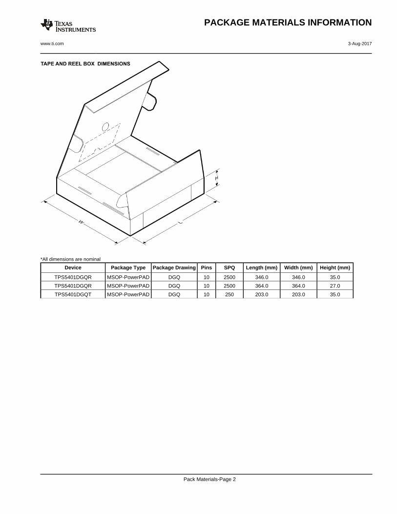
*All dimensions are nominal
Device Package Type Package Drawing Pins SPQ Length (mm) Width (mm) Height (mm)
TPS5401DGQR MSOP-PowerPAD DGQ 10 2500 346.0 346.0 35.0
TPS5401DGQR MSOP-PowerPAD DGQ 10 2500 364.0 364.0 27.0
TPS5401DGQT MSOP-PowerPAD DGQ 10 250 203.0 203.0 35.0
PACKAGE MATERIALS INFORMATION
www.ti.com 3-Aug-2017
Pack Materials-Page 2

IMPORTANT NOTICE
Texas Instruments Incorporated (TI) reserves the right to make corrections, enhancements, improvements and other changes to itssemiconductor products and services per JESD46, latest issue, and to discontinue any product or service per JESD48, latest issue. Buyersshould obtain the latest relevant information before placing orders and should verify that such information is current and complete.TI’s published terms of sale for semiconductor products (http://www.ti.com/sc/docs/stdterms.htm) apply to the sale of packaged integratedcircuit products that TI has qualified and released to market. Additional terms may apply to the use or sale of other types of TI products andservices.Reproduction of significant portions of TI information in TI data sheets is permissible only if reproduction is without alteration and isaccompanied by all associated warranties, conditions, limitations, and notices. TI is not responsible or liable for such reproduceddocumentation. Information of third parties may be subject to additional restrictions. Resale of TI products or services with statementsdifferent from or beyond the parameters stated by TI for that product or service voids all express and any implied warranties for theassociated TI product or service and is an unfair and deceptive business practice. TI is not responsible or liable for any such statements.Buyers and others who are developing systems that incorporate TI products (collectively, “Designers”) understand and agree that Designersremain responsible for using their independent analysis, evaluation and judgment in designing their applications and that Designers havefull and exclusive responsibility to assure the safety of Designers' applications and compliance of their applications (and of all TI productsused in or for Designers’ applications) with all applicable regulations, laws and other applicable requirements. Designer represents that, withrespect to their applications, Designer has all the necessary expertise to create and implement safeguards that (1) anticipate dangerousconsequences of failures, (2) monitor failures and their consequences, and (3) lessen the likelihood of failures that might cause harm andtake appropriate actions. Designer agrees that prior to using or distributing any applications that include TI products, Designer willthoroughly test such applications and the functionality of such TI products as used in such applications.TI’s provision of technical, application or other design advice, quality characterization, reliability data or other services or information,including, but not limited to, reference designs and materials relating to evaluation modules, (collectively, “TI Resources”) are intended toassist designers who are developing applications that incorporate TI products; by downloading, accessing or using TI Resources in anyway, Designer (individually or, if Designer is acting on behalf of a company, Designer’s company) agrees to use any particular TI Resourcesolely for this purpose and subject to the terms of this Notice.TI’s provision of TI Resources does not expand or otherwise alter TI’s applicable published warranties or warranty disclaimers for TIproducts, and no additional obligations or liabilities arise from TI providing such TI Resources. TI reserves the right to make corrections,enhancements, improvements and other changes to its TI Resources. TI has not conducted any testing other than that specificallydescribed in the published documentation for a particular TI Resource.Designer is authorized to use, copy and modify any individual TI Resource only in connection with the development of applications thatinclude the TI product(s) identified in such TI Resource. NO OTHER LICENSE, EXPRESS OR IMPLIED, BY ESTOPPEL OR OTHERWISETO ANY OTHER TI INTELLECTUAL PROPERTY RIGHT, AND NO LICENSE TO ANY TECHNOLOGY OR INTELLECTUAL PROPERTYRIGHT OF TI OR ANY THIRD PARTY IS GRANTED HEREIN, including but not limited to any patent right, copyright, mask work right, orother intellectual property right relating to any combination, machine, or process in which TI products or services are used. Informationregarding or referencing third-party products or services does not constitute a license to use such products or services, or a warranty orendorsement thereof. Use of TI Resources may require a license from a third party under the patents or other intellectual property of thethird party, or a license from TI under the patents or other intellectual property of TI.TI RESOURCES ARE PROVIDED “AS IS” AND WITH ALL FAULTS. TI DISCLAIMS ALL OTHER WARRANTIES ORREPRESENTATIONS, EXPRESS OR IMPLIED, REGARDING RESOURCES OR USE THEREOF, INCLUDING BUT NOT LIMITED TOACCURACY OR COMPLETENESS, TITLE, ANY EPIDEMIC FAILURE WARRANTY AND ANY IMPLIED WARRANTIES OFMERCHANTABILITY, FITNESS FOR A PARTICULAR PURPOSE, AND NON-INFRINGEMENT OF ANY THIRD PARTY INTELLECTUALPROPERTY RIGHTS. TI SHALL NOT BE LIABLE FOR AND SHALL NOT DEFEND OR INDEMNIFY DESIGNER AGAINST ANY CLAIM,INCLUDING BUT NOT LIMITED TO ANY INFRINGEMENT CLAIM THAT RELATES TO OR IS BASED ON ANY COMBINATION OFPRODUCTS EVEN IF DESCRIBED IN TI RESOURCES OR OTHERWISE. IN NO EVENT SHALL TI BE LIABLE FOR ANY ACTUAL,DIRECT, SPECIAL, COLLATERAL, INDIRECT, PUNITIVE, INCIDENTAL, CONSEQUENTIAL OR EXEMPLARY DAMAGES INCONNECTION WITH OR ARISING OUT OF TI RESOURCES OR USE THEREOF, AND REGARDLESS OF WHETHER TI HAS BEENADVISED OF THE POSSIBILITY OF SUCH DAMAGES.Unless TI has explicitly designated an individual product as meeting the requirements of a particular industry standard (e.g., ISO/TS 16949and ISO 26262), TI is not responsible for any failure to meet such industry standard requirements.Where TI specifically promotes products as facilitating functional safety or as compliant with industry functional safety standards, suchproducts are intended to help enable customers to design and create their own applications that meet applicable functional safety standardsand requirements. Using products in an application does not by itself establish any safety features in the application. Designers mustensure compliance with safety-related requirements and standards applicable to their applications. Designer may not use any TI products inlife-critical medical equipment unless authorized officers of the parties have executed a special contract specifically governing such use.Life-critical medical equipment is medical equipment where failure of such equipment would cause serious bodily injury or death (e.g., lifesupport, pacemakers, defibrillators, heart pumps, neurostimulators, and implantables). Such equipment includes, without limitation, allmedical devices identified by the U.S. Food and Drug Administration as Class III devices and equivalent classifications outside the U.S.TI may expressly designate certain products as completing a particular qualification (e.g., Q100, Military Grade, or Enhanced Product).Designers agree that it has the necessary expertise to select the product with the appropriate qualification designation for their applicationsand that proper product selection is at Designers’ own risk. Designers are solely responsible for compliance with all legal and regulatoryrequirements in connection with such selection.Designer will fully indemnify TI and its representatives against any damages, costs, losses, and/or liabilities arising out of Designer’s non-compliance with the terms and provisions of this Notice.
Mailing Address: Texas Instruments, Post Office Box 655303, Dallas, Texas 75265Copyright © 2017, Texas Instruments Incorporated