Embed Size (px)
Citation preview

SW
BOOT
LDRV
PGND
HDRV
VIN
UVLO
PGOOD
VBP
ILIM
TRK
SS
FB
RT
M/S
COMP
AGND
SYNC
VDD
ENABLE
2
3
4
5
6
7
8
9
1 20
19
18
17
16
15
14
13
12
TPS40170
10 11
VOUT
VIN
UDG-09219
70
75
80
85
90
95
100
0 1 2 3 4 5 6
Load Current (A)
Effic
iency (
%)
VIN = 12 V
VIN = 24 V
VIN = 48 V
Product
Folder
Order
Now
Technical
Documents
Tools &
Software
Support &Community
An IMPORTANT NOTICE at the end of this data sheet addresses availability, warranty, changes, use in safety-critical applications,intellectual property matters and other important disclaimers. PRODUCTION DATA.
TPS40170SLUS970B –NOVEMBER 2013–REVISED DECEMBER 2014
TPS40170 4.5 V to 60 V Wide Input Synchronous PWM Buck Controller
1
1 Features1• Wide Input Voltage Range from 4.5 V to 60 V• 600 mV Reference Voltage with 1% Accuracy• Programmable UVLO and Hysteresis• Voltage Mode Control With Voltage Feed Forward• Programmable Frequency Between 100 kHz and
600 kHz• Bi-directional -Frequency Synchronization With
Master/Slave Option• Low-side FET Sensing Overcurrent Protection and
High-Side FET Sensing Short-Circuit ProtectionWith Integrated Thermal Compensation
• Programmable Closed Loop Soft-Start• Supports Pre-Biased Outputs• Thermal Shutdown at 165°C with Hysteresis• Voltage Tracking• Powergood• ENABLE with 1-µA Low Current Shutdown• 8.0-V and 3.3-V LDO Output• Integrated Bootstrap Diode• 20-Pin 3.5 mm × 4.5 mm VQFN (RGY) Package• Create a Custom Design Using the TPS40170
with the WEBENCH Power Designer
2 Applications• POL Modules• Wide Input Voltage, High-Power Density DC - DC
Converters for Industrial, Networking and TelecomEquipment
3 DescriptionTPS40170 is a full-featured, synchronous PWM buckcontroller that operates at an input voltage between4.5 V and 60 V and is optimized for high-powerdensity, high-reliability DC-DC converter applications.The controller implements voltage-mode control withinput voltage feed-forward compensation that enablesinstant response to input voltage change. Theswitching frequency is programmable from 100 kHz to600 kHz.
The TPS40170 has a complete set of systemprotection and monitoring features such asprogrammable undervoltage lockout (UVLO),programmable overcurrent protection (OCP) bysensing the low-side FET, selectable short-circuitprotection (SCP) by sensing the high-side FET andthermal shutdown. The ENABLE pin allows forsystem shutdown in a low-current (1 µA typical)mode. The controller supports pre-biased output,provides an open-drain PGOOD signal, and hasclosed-loop soft-start, output voltage tracking andadaptive dead-time control.
TPS40170 provides accurate output voltageregulation through 1% ensured accuracy.Additionally, the controller implements a novelscheme of bi-directional synchronization with onecontroller acting as the master and other downstreamcontrollers acting as slaves synchronized to themaster in-phase or 180° out-of-phase. Slavecontrollers can be synchronized to an external clockwithin ±30% of the free-running switching frequency.
Device Information(1)
PART NUMBER PACKAGE BODY SIZE (NOM)TPS40170 VQFN (20) 3.50 mm × 4.50 mm
(1) For all available packages, see the orderable addendum atthe end of the datasheet.
Simplified Application Efficiency vs. Load Current

2
TPS40170SLUS970B –NOVEMBER 2013–REVISED DECEMBER 2014 www.ti.com
Product Folder Links: TPS40170
Submit Documentation Feedback Copyright © 2013–2014, Texas Instruments Incorporated
Table of Contents1 Features .................................................................. 12 Applications ........................................................... 13 Description ............................................................. 14 Revision History..................................................... 25 Pin Configuration and Functions ......................... 36 Specifications......................................................... 4
6.1 Absolute Maximum Ratings ...................................... 46.2 Handling Ratings ...................................................... 46.3 Recommended Operating Conditions....................... 46.4 Thermal Information .................................................. 56.5 Electrical Characteristics........................................... 56.6 Typical Characteristics .............................................. 8
7 Detailed Description ............................................ 117.1 Overview ................................................................. 117.2 Functional Block Diagram ....................................... 117.3 Feature Description................................................. 12
7.4 Device Functional Modes........................................ 278 Application and Implementation ........................ 29
8.1 Application Information............................................ 298.2 Typical Application ................................................. 30
9 Power Supply Recommendations ...................... 3710 Layout................................................................... 37
10.1 Layout Guidelines ................................................. 3710.2 Layout Example .................................................... 37
11 Device and Documentation Support ................. 4011.1 Device Support...................................................... 4011.2 Documentation Support ....................................... 4011.3 Trademarks ........................................................... 4011.4 Electrostatic Discharge Caution............................ 4011.5 Glossary ................................................................ 41
12 Mechanical, Packaging, and OrderableInformation ........................................................... 41
4 Revision History
Changes from Revision A (November 2013) to Revision B Page
• Added Handling Ratings table, Feature Description section, Device Functional Modes, Application andImplementation section, Power Supply Recommendations section, Layout section, Device and DocumentationSupport section, and Mechanical, Packaging, and Orderable Information section................................................................ 3
Changes from Original (March 2011) to Revision A Page
• Deleted Ordering Information table. Replaced with Package Option Addenda inserted after the last page of this datasheet. ..................................................................................................................................................................................... 3
• Added clarity to Figure 20..................................................................................................................................................... 16• Added significant clarity to and corrected typographic errors in DESIGN EXAMPLE ......................................................... 32
19
18
17
16
15
14
13
12
1 202
3
4
5
6
7
8
109 11
SW
BOOT
LDRV
PGND
HDRV
VIN
UVLO
PGOOD
VBP
ILIM
TRK
SS
FB
RT
M/S
COMP
AGND
SYNC
VDD
ENABLE
TPS40170
3
TPS40170www.ti.com SLUS970B –NOVEMBER 2013–REVISED DECEMBER 2014
Product Folder Links: TPS40170
Submit Documentation FeedbackCopyright © 2013–2014, Texas Instruments Incorporated
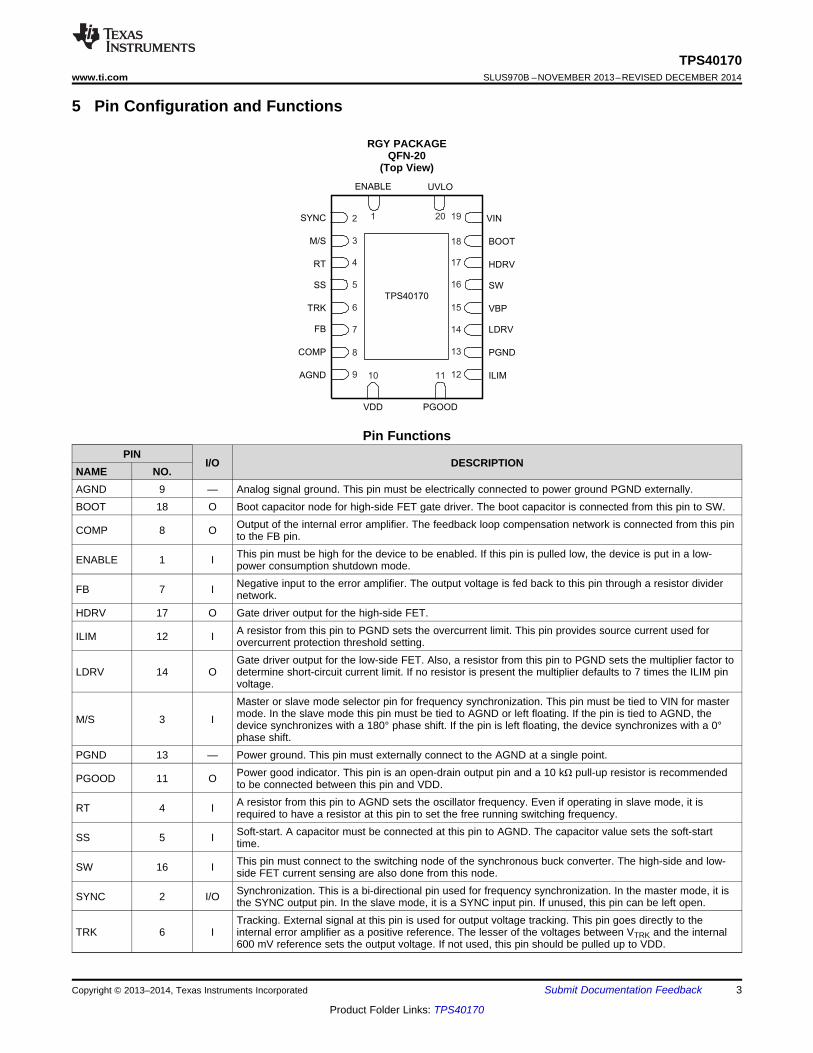
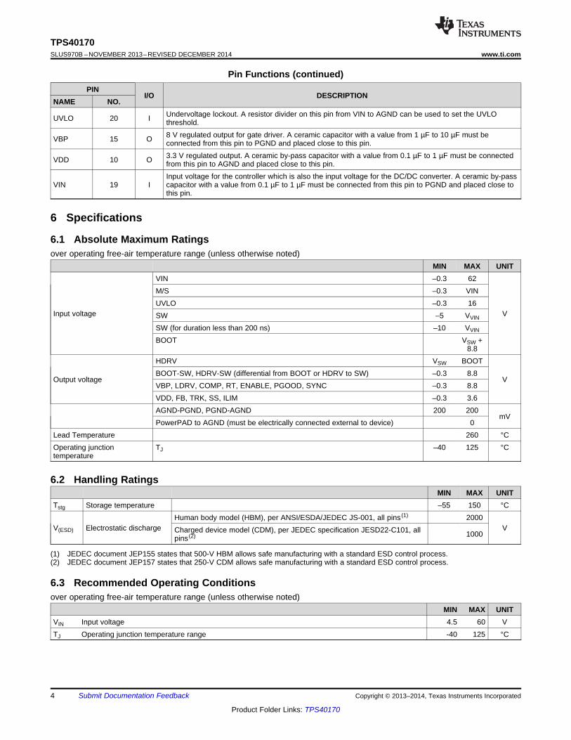
5 Pin Configuration and Functions
RGY PACKAGEQFN-20
(Top View)
Pin FunctionsPIN
I/O DESCRIPTIONNAME NO.AGND 9 — Analog signal ground. This pin must be electrically connected to power ground PGND externally.BOOT 18 O Boot capacitor node for high-side FET gate driver. The boot capacitor is connected from this pin to SW.
COMP 8 O Output of the internal error amplifier. The feedback loop compensation network is connected from this pinto the FB pin.
ENABLE 1 I This pin must be high for the device to be enabled. If this pin is pulled low, the device is put in a low-power consumption shutdown mode.
FB 7 I Negative input to the error amplifier. The output voltage is fed back to this pin through a resistor dividernetwork.
HDRV 17 O Gate driver output for the high-side FET.
ILIM 12 I A resistor from this pin to PGND sets the overcurrent limit. This pin provides source current used forovercurrent protection threshold setting.
LDRV 14 OGate driver output for the low-side FET. Also, a resistor from this pin to PGND sets the multiplier factor todetermine short-circuit current limit. If no resistor is present the multiplier defaults to 7 times the ILIM pinvoltage.
M/S 3 I
Master or slave mode selector pin for frequency synchronization. This pin must be tied to VIN for mastermode. In the slave mode this pin must be tied to AGND or left floating. If the pin is tied to AGND, thedevice synchronizes with a 180° phase shift. If the pin is left floating, the device synchronizes with a 0°phase shift.
PGND 13 — Power ground. This pin must externally connect to the AGND at a single point.
PGOOD 11 O Power good indicator. This pin is an open-drain output pin and a 10 kΩ pull-up resistor is recommendedto be connected between this pin and VDD.
RT 4 I A resistor from this pin to AGND sets the oscillator frequency. Even if operating in slave mode, it isrequired to have a resistor at this pin to set the free running switching frequency.
SS 5 I Soft-start. A capacitor must be connected at this pin to AGND. The capacitor value sets the soft-starttime.
SW 16 I This pin must connect to the switching node of the synchronous buck converter. The high-side and low-side FET current sensing are also done from this node.
SYNC 2 I/O Synchronization. This is a bi-directional pin used for frequency synchronization. In the master mode, it isthe SYNC output pin. In the slave mode, it is a SYNC input pin. If unused, this pin can be left open.
TRK 6 ITracking. External signal at this pin is used for output voltage tracking. This pin goes directly to theinternal error amplifier as a positive reference. The lesser of the voltages between VTRK and the internal600 mV reference sets the output voltage. If not used, this pin should be pulled up to VDD.
4
TPS40170SLUS970B –NOVEMBER 2013–REVISED DECEMBER 2014 www.ti.com
Product Folder Links: TPS40170
Submit Documentation Feedback Copyright © 2013–2014, Texas Instruments Incorporated
Pin Functions (continued)PIN
I/O DESCRIPTIONNAME NO.
UVLO 20 I Undervoltage lockout. A resistor divider on this pin from VIN to AGND can be used to set the UVLOthreshold.
VBP 15 O 8 V regulated output for gate driver. A ceramic capacitor with a value from 1 µF to 10 µF must beconnected from this pin to PGND and placed close to this pin.
VDD 10 O 3.3 V regulated output. A ceramic by-pass capacitor with a value from 0.1 µF to 1 µF must be connectedfrom this pin to AGND and placed close to this pin.
VIN 19 IInput voltage for the controller which is also the input voltage for the DC/DC converter. A ceramic by-passcapacitor with a value from 0.1 µF to 1 µF must be connected from this pin to PGND and placed close tothis pin.
6 Specifications
6.1 Absolute Maximum Ratingsover operating free-air temperature range (unless otherwise noted)
MIN MAX UNIT
Input voltage
VIN –0.3 62
V
M/S –0.3 VINUVLO –0.3 16SW –5 VVIN
SW (for duration less than 200 ns) –10 VVIN
BOOT VSW +8.8
Output voltage
HDRV VSW BOOT
VBOOT-SW, HDRV-SW (differential from BOOT or HDRV to SW) –0.3 8.8VBP, LDRV, COMP, RT, ENABLE, PGOOD, SYNC –0.3 8.8VDD, FB, TRK, SS, ILIM –0.3 3.6AGND-PGND, PGND-AGND 200 200
mVPowerPAD to AGND (must be electrically connected external to device) 0
Lead Temperature 260 °COperating junctiontemperature
TJ –40 125 °C
(1) JEDEC document JEP155 states that 500-V HBM allows safe manufacturing with a standard ESD control process.(2) JEDEC document JEP157 states that 250-V CDM allows safe manufacturing with a standard ESD control process.
6.2 Handling RatingsMIN MAX UNIT
Tstg Storage temperature –55 150 °C
V(ESD) Electrostatic dischargeHuman body model (HBM), per ANSI/ESDA/JEDEC JS-001, all pins (1) 2000
VCharged device model (CDM), per JEDEC specification JESD22-C101, allpins (2) 1000
6.3 Recommended Operating Conditionsover operating free-air temperature range (unless otherwise noted)
MIN MAX UNITVIN Input voltage 4.5 60 VTJ Operating junction temperature range -40 125 °C
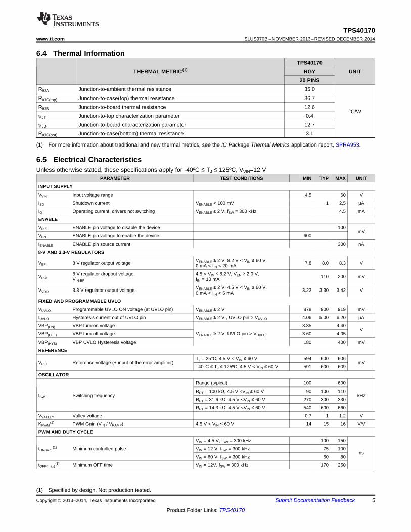
5
TPS40170www.ti.com SLUS970B –NOVEMBER 2013–REVISED DECEMBER 2014
Product Folder Links: TPS40170
Submit Documentation FeedbackCopyright © 2013–2014, Texas Instruments Incorporated
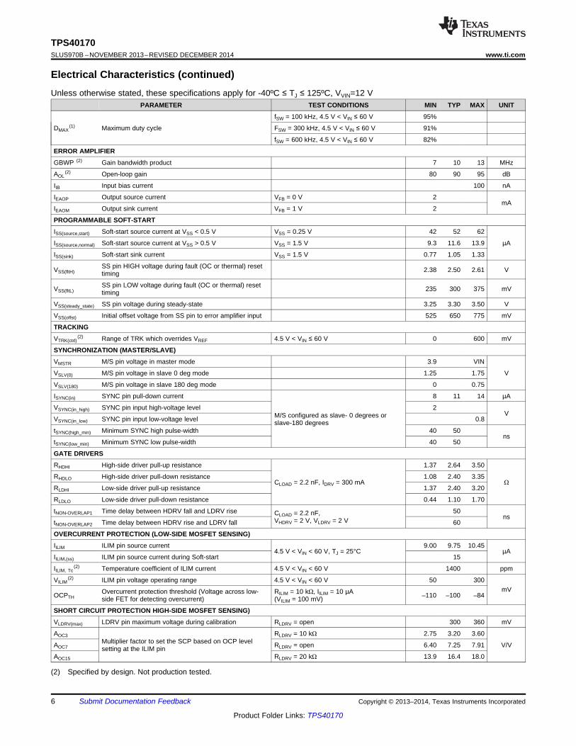
(1) For more information about traditional and new thermal metrics, see the IC Package Thermal Metrics application report, SPRA953.
6.4 Thermal Information
THERMAL METRIC (1)TPS40170
UNITRGY20 PINS
RθJA Junction-to-ambient thermal resistance 35.0
°C/W
RθJC(top) Junction-to-case(top) thermal resistance 36.7RθJB Junction-to-board thermal resistance 12.6ψJT Junction-to-top characterization parameter 0.4ψJB Junction-to-board characterization parameter 12.7RθJC(bot) Junction-to-case(bottom) thermal resistance 3.1
(1) Specified by design. Not production tested.
6.5 Electrical CharacteristicsUnless otherwise stated, these specifications apply for -40ºC ≤ TJ ≤ 125ºC, VVIN=12 V
PARAMETER TEST CONDITIONS MIN TYP MAX UNIT
INPUT SUPPLY
VVIN Input voltage range 4.5 60 V
ISD Shutdown current VENABLE < 100 mV 1 2.5 µA
IQ Operating current, drivers not switching VENABLE ≥ 2 V, fSW = 300 kHz 4.5 mA
ENABLE
VDIS ENABLE pin voltage to disable the device 100mV
VEN ENABLE pin voltage to enable the device 600
IENABLE ENABLE pin source current 300 nA
8-V AND 3.3-V REGULATORS
VBP 8 V regulator output voltage VENABLE ≥ 2 V, 8.2 V < VIN ≤ 60 V,0 mA < IIN < 20 mA 7.8 8.0 8.3 V
VDO8 V regulator dropout voltage,VIN-BP
4.5 < VIN ≤ 8.2 V, VEN ≥ 2.0 V,IIN = 10 mA 110 200 mV
VVDD 3.3 V regulator output voltage VENABLE ≥ 2 V, 4.5 V < VIN ≤ 60 V,0 mA < IIN < 5 mA 3.22 3.30 3.42 V
FIXED AND PROGRAMMABLE UVLO
VUVLO Programmable UVLO ON voltage (at UVLO pin) VENABLE ≥ 2 V 878 900 919 mV
IUVLO Hysteresis current out of UVLO pin VENABLE ≥ 2 V , UVLO pin > VUVLO 4.06 5.00 6.20 µA
VBP(ON) VBP turn-on voltage
VENABLE ≥ 2 V, UVLO pin > VUVLO
3.85 4.40V
VBP(OFF) VBP turn-off voltage 3.60 4.05
VBP(HYS) VBP UVLO Hysteresis voltage 180 400 mV
REFERENCE
VREF Reference voltage (+ input of the error amplifier)TJ = 25°C, 4.5 V < VIN ≤ 60 V 594 600 606
mV–40°C ≤ TJ ≤ 125ºC, 4.5 V < VIN ≤ 60 V 591 600 609
OSCILLATOR
fSW Switching frequency
Range (typical) 100 600
kHzRRT = 100 kΩ, 4.5 V <VIN ≤ 60 V 90 100 110
RRT = 31.6 kΩ, 4.5 V <VIN ≤ 60 V 270 300 330
RRT = 14.3 kΩ, 4.5 V <VIN ≤ 60 V 540 600 660
VVALLEY Valley voltage 0.7 1 1.2 V
KPWM(1) PWM Gain (VIN / VRAMP) 4.5 V < VIN ≤ 60 V 14 15 16 V/V
PWM AND DUTY CYCLE
tON(min)(1) Minimum controlled pulse
VIN = 4.5 V, fSW = 300 kHz 100 150
nsVIN = 12 V, fSW = 300 kHz 75 100
VIN = 60 V, fSW = 300 kHz 50 80
tOFF(max)(1) Minimum OFF time VIN = 12V, fSW = 300 kHz 170 250
6
TPS40170SLUS970B –NOVEMBER 2013–REVISED DECEMBER 2014 www.ti.com
Product Folder Links: TPS40170
Submit Documentation Feedback Copyright © 2013–2014, Texas Instruments Incorporated
Electrical Characteristics (continued)Unless otherwise stated, these specifications apply for -40ºC ≤ TJ ≤ 125ºC, VVIN=12 V
PARAMETER TEST CONDITIONS MIN TYP MAX UNIT
(2) Specified by design. Not production tested.
DMAX(1) Maximum duty cycle
fSW = 100 kHz, 4.5 V < VIN ≤ 60 V 95%
FSW = 300 kHz, 4.5 V < VIN ≤ 60 V 91%
fSW = 600 kHz, 4.5 V < VIN ≤ 60 V 82%
ERROR AMPLIFIER
GBWP (2) Gain bandwidth product 7 10 13 MHz
AOL(2) Open-loop gain 80 90 95 dB
IIB Input bias current 100 nA
IEAOP Output source current VFB = 0 V 2mA
IEAOM Output sink current VFB = 1 V 2
PROGRAMMABLE SOFT-START
ISS(source,start) Soft-start source current at VSS < 0.5 V VSS = 0.25 V 42 52 62
µAISS(source,normal) Soft-start source current at VSS > 0.5 V VSS = 1.5 V 9.3 11.6 13.9
ISS(sink) Soft-start sink current VSS = 1.5 V 0.77 1.05 1.33
VSS(fltH)SS pin HIGH voltage during fault (OC or thermal) resettiming 2.38 2.50 2.61 V
VSS(fltL)SS pin LOW voltage during fault (OC or thermal) resettiming 235 300 375 mV
VSS(steady_state) SS pin voltage during steady-state 3.25 3.30 3.50 V
VSS(offst) Initial offset voltage from SS pin to error amplifier input 525 650 775 mV
TRACKING
VTRK(ctrl)(2) Range of TRK which overrides VREF 4.5 V < VIN ≤ 60 V 0 600 mV
SYNCHRONIZATION (MASTER/SLAVE)
VMSTR M/S pin voltage in master mode 3.9 VIN
VVSLV(0) M/S pin voltage in slave 0 deg mode 1.25 1.75
VSLV(180) M/S pin voltage in slave 180 deg mode 0 0.75
ISYNC(in) SYNC pin pull-down current
M/S configured as slave- 0 degrees orslave-180 degrees
8 11 14 µA
VSYNC(in_high) SYNC pin input high-voltage level 2V
VSYNC(in_low) SYNC pin input low-voltage level 0.8
tSYNC(high_min) Minimum SYNC high pulse-width 40 50ns
tSYNC(low_min) Minimum SYNC low pulse-width 40 50
GATE DRIVERS
RHDHI High-side driver pull-up resistance
CLOAD = 2.2 nF, IDRV = 300 mA
1.37 2.64 3.50
ΩRHDLO High-side driver pull-down resistance 1.08 2.40 3.35
RLDHI Low-side driver pull-up resistance 1.37 2.40 3.20
RLDLO Low-side driver pull-down resistance 0.44 1.10 1.70
tNON-OVERLAP1 Time delay between HDRV fall and LDRV rise CLOAD = 2.2 nF,VHDRV = 2 V, VLDRV = 2 V
50ns
tNON-OVERLAP2 Time delay between HDRV rise and LDRV fall 60
OVERCURRENT PROTECTION (LOW-SIDE MOSFET SENSING)
IILIM ILIM pin source current4.5 V < VIN < 60 V, TJ = 25°C
9.00 9.75 10.45µA
IILIM,(ss) ILIM pin source current during Soft-start 15
IILIM, Tc(2) Temperature coefficient of ILIM current 4.5 V < VIN < 60 V 1400 ppm
VILIM(2) ILIM pin voltage operating range 4.5 V < VIN < 60 V 50 300
mVOCPTH
Overcurrent protection threshold (Voltage across low-side FET for detecting overcurrent)
RILIM = 10 kΩ, IILIM = 10 µA(VILIM = 100 mV) –110 –100 –84
SHORT CIRCUIT PROTECTION HIGH-SIDE MOSFET SENSING)
VLDRV(max) LDRV pin maximum voltage during calibration RLDRV = open 300 360 mV
AOC3Multiplier factor to set the SCP based on OCP levelsetting at the ILIM pin
RLDRV = 10 kΩ 2.75 3.20 3.60
V/VAOC7 RLDRV = open 6.40 7.25 7.91
AOC15 RLDRV = 20 kΩ 13.9 16.4 18.0
7
TPS40170www.ti.com SLUS970B –NOVEMBER 2013–REVISED DECEMBER 2014
Product Folder Links: TPS40170
Submit Documentation FeedbackCopyright © 2013–2014, Texas Instruments Incorporated
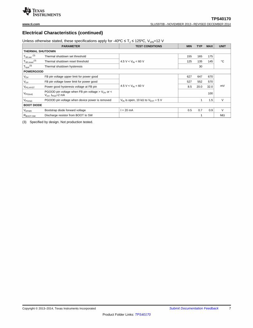
Electrical Characteristics (continued)Unless otherwise stated, these specifications apply for -40ºC ≤ TJ ≤ 125ºC, VVIN=12 V
PARAMETER TEST CONDITIONS MIN TYP MAX UNIT
(3) Specified by design. Not production tested.
THERMAL SHUTDOWN
TSD,set(3) Thermal shutdown set threshold
4.5 V < VIN < 60 V
155 165 175
°CTSD,reset(3) Thermal shutdown reset threshold 125 135 145
Thyst(3) Thermal shutdown hysteresis 30
POWERGOOD
VOV FB pin voltage upper limit for power good
4.5 V < VIN < 60 V
627 647 670
mVVUV FB pin voltage lower limit for power good 527 552 570
VPG,HYST Power good hysteresis voltage at FB pin 8.5 20.0 32.0
VPG(out)PGOOD pin voltage when FB pin voltage > VOV or <VUV, IPGD=2 mA 100
VPG(np) PGOOD pin voltage when device power is removed VIN is open, 10 kΩ to VEXT = 5 V 1 1.5 V
BOOT DIODE
VDFWD Bootstrap diode forward voltage I = 20 mA 0.5 0.7 0.9 V
RBOOT-SW Discharge resistor from BOOT to SW 1 MΩ
0.9
1.0
1.1
1.2
1.3
1.4
−40 −25 −10 5 20 35 50 65 80 95 110 125Temperature (°C)
Shu
tdow
n C
urre
nt (
µA)
VIN = 12 V3.10
3.12
3.14
3.16
3.18
3.20
3.22
3.24
3.26
3.28
−40 −25 −10 5 20 35 50 65 80 95 110 125Junction Temperature (°C)
Ope
ratin
g C
urre
nt (
mA
)
VIN = 12 VfSW = 300 kHz
280
282
284
286
288
290
292
294
296
298
300
302
−40 −25 −10 5 20 35 50 65 80 95 110 125Junction Temperature (°C)
Sw
itchi
ng F
requ
ency
(kH
z)
VIN = 4.5 VVIN = 24 VVIN = 60 V
fSW= 300 kHz554
558
562
566
570
574
578
582
586
590
594
598
602
606
−40 −25 −10 5 20 35 50 65 80 95 110 125Junction Temperature (°C)
Sw
itchi
ng F
requ
ency
(kH
z)
VIN = 4.5 VVIN = 24 VVIN = 60 V
fSW= 600 kHz
598.5
598.8
599.0
599.2
599.5
599.8
600.0
−40 −25 −10 5 20 35 50 65 80 95 110 125Temperature (°C)
Ref
eren
ce V
olta
ge (
mV
)
95.0
95.5
96.0
96.5
97.0
97.5
98.0
98.5
99.0
99.5
100.0
−40 −25 −10 5 20 35 50 65 80 95 110 125Junction Temperature (°C)
Sw
itchi
ng F
requ
ency
(kH
z)
VIN = 4.5 VVIN = 24 VVIN = 60 V
fSW= 100 kHz
8
TPS40170SLUS970B –NOVEMBER 2013–REVISED DECEMBER 2014 www.ti.com
Product Folder Links: TPS40170
Submit Documentation Feedback Copyright © 2013–2014, Texas Instruments Incorporated
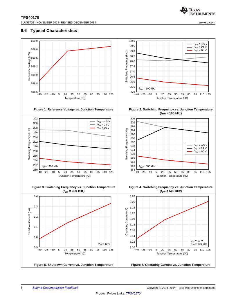
6.6 Typical Characteristics
Figure 1. Reference Voltage vs. Junction Temperature Figure 2. Switching Frequency vs. Junction Temperature(fSW = 100 kHz)
Figure 3. Switching Frequency vs. Junction Temperature(fSW = 300 kHz)
Figure 4. Switching Frequency vs. Junction Temperature(fSW = 600 kHz)
Figure 5. Shutdown Current vs. Junction Temperature Figure 6. Operating Current vs. Junction Temperature
11.60
11.64
11.68
11.72
11.76
11.80
11.84
−40 −25 −10 5 20 35 50 65 80 95 110 125Junction Temperature (°C)
Sof
t−S
tart
Sou
rce
Cur
rent
(µA
)
VSS > 0.5 V51.00
51.25
51.50
51.75
52.00
52.25
52.50
52.75
53.00
−40 −25 −10 5 20 35 50 65 80 95 110 125Junction Temperature (°C)
Sof
t−S
tart
Sou
rce
Cur
rent
(µA
)
VSS < 0.5 V
4.08
4.09
4.10
4.11
4.12
4.13
4.14
4.15
−40 −25 −10 5 20 35 50 65 80 95 110 125Junction Temperature (°C)
VB
P T
urn−
On
Vol
tage
(V
)
275
280
285
290
295
300
305
310
315
320
325
330
−40 −25 −10 5 20 35 50 65 80 95 110 125Junction Temperature (°C)
VB
P U
VLO
Hys
tere
sis
Vol
tage
(m
V)
895.0
895.5
896.0
896.5
897.0
897.5
898.0
−40 −25 −10 5 20 35 50 65 80 95 110 125Junction Temperature (°C)
UV
LO O
n V
olta
ge (
mV
)
4.98
5.00
5.02
5.04
5.06
5.08
5.10
5.12
5.14
5.16
−40 −25 −10 5 20 35 50 65 80 95 110 125Junction Temperature (°C)
UV
LO H
yste
resi
s C
urre
nt (
µA)
9
TPS40170www.ti.com SLUS970B –NOVEMBER 2013–REVISED DECEMBER 2014
Product Folder Links: TPS40170
Submit Documentation FeedbackCopyright © 2013–2014, Texas Instruments Incorporated
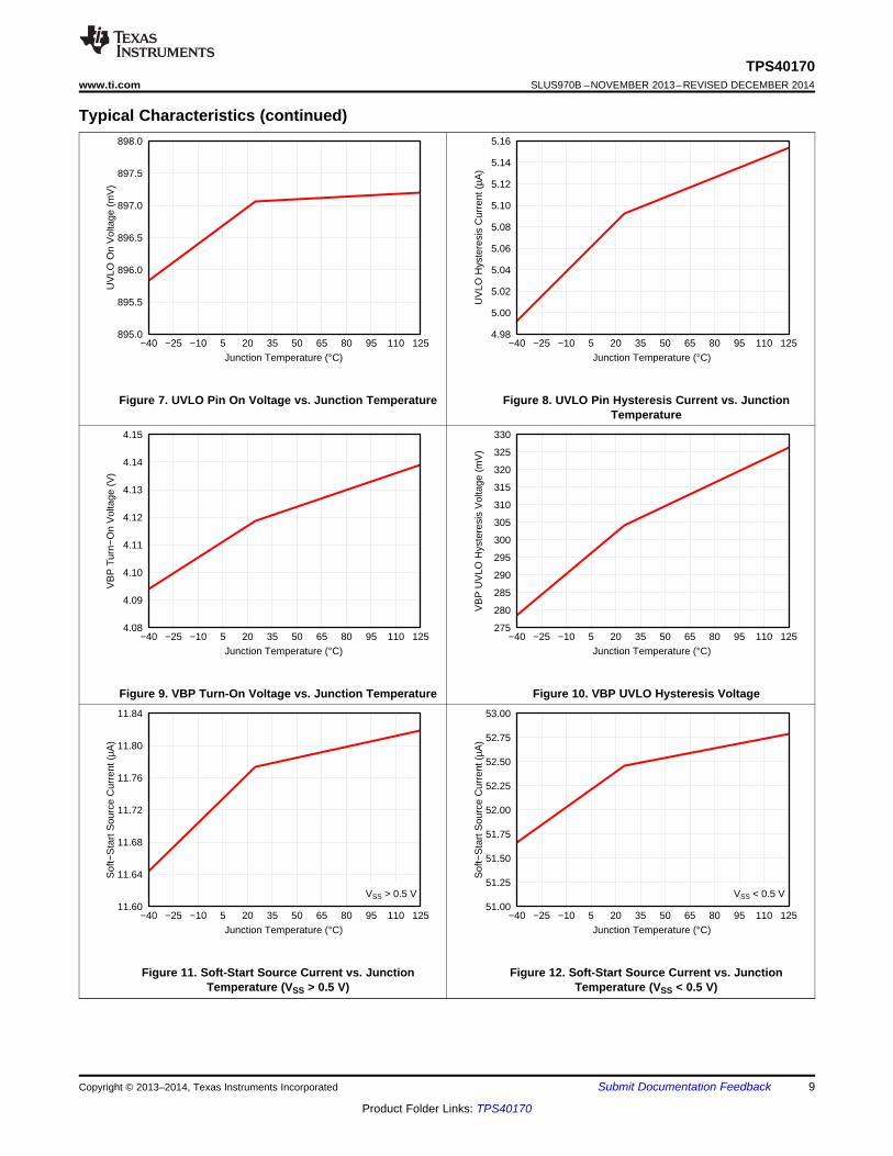
Typical Characteristics (continued)
Figure 7. UVLO Pin On Voltage vs. Junction Temperature Figure 8. UVLO Pin Hysteresis Current vs. JunctionTemperature
Figure 9. VBP Turn-On Voltage vs. Junction Temperature Figure 10. VBP UVLO Hysteresis Voltage
Figure 11. Soft-Start Source Current vs. JunctionTemperature (VSS > 0.5 V)
Figure 12. Soft-Start Source Current vs. JunctionTemperature (VSS < 0.5 V)
525
550
575
600
625
650
675
−40 −25 −10 5 20 35 50 65 80 95 110 125Junction Temperature (°C)
Pow
er G
ood
Thr
esho
ld V
olta
ge (
mV
)
OvervoltageUndervoltage
8.4
8.7
9.0
9.3
9.6
9.9
10.2
10.5
10.8
11.1
−40 −25 −10 5 20 35 50 65 80 95 110 125Junction Temperature (°C)
ILIM
Sou
rce
Cur
rent
(µA
)
614
620
626
632
638
644
650
656
662
668
674
680
−40 −25 −10 5 20 35 50 65 80 95 110 125Junction Temperature (°C)
Sof
t−S
tart
Initi
al O
ffset
Vol
tage
(m
V)
10
TPS40170SLUS970B –NOVEMBER 2013–REVISED DECEMBER 2014 www.ti.com
Product Folder Links: TPS40170
Submit Documentation Feedback Copyright © 2013–2014, Texas Instruments Incorporated
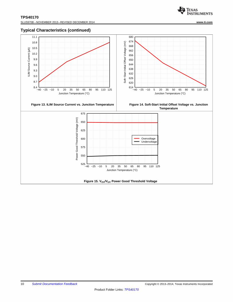
Typical Characteristics (continued)
Figure 13. ILIM Source Current vs. Junction Temperature Figure 14. Soft-Start Initial Offset Voltage vs. JunctionTemperature
Figure 15. VOV/VUV Power Good Threshold Voltage

UDG-09218
1 19 20
8-V
Regulator
3.3-V
Regulator
Input and
Regulators OK
ENABLE VIN UVLO
10VDD
4RT
2SYNC
3M/S
Oscillator
and
Synchronization
Run
+
PWM Logic
Anti-Cross
Conduction
Run
Fault
VIN
+++
TRK Error
Amplifier
6
SSEAMPVREF
FB 7
RunCOMP 8
AGND 9
Over-Temperature
Fault Controller
TJ
CLK
Overcurrent
Fault Controller
VINRun
SW
LDRVCLK
12ILIM
Run
OC_FAULT
Soft-Start
and
Fault Logic
T_FAULTPower Good
Controller
VREF
FB
18 BOOT
17 HDRV
16 SW
15 VBP
14 LDRV
13 PGND
Gate Drivers
VBP
Run
Run
11 PGOOD
5 SS
SSEAMP
CLK
RAMP
TPS40170
VBP
PWM
Comparator
FAULT
FAULT
Reset
Run
Run
11
TPS40170www.ti.com SLUS970B –NOVEMBER 2013–REVISED DECEMBER 2014
Product Folder Links: TPS40170
Submit Documentation FeedbackCopyright © 2013–2014, Texas Instruments Incorporated
7 Detailed Description
7.1 OverviewThe TPS40170 is a synchronous PWM buck controller that accepts a wide range of input voltage from 4.5 V to60 V and features voltage-mode control with input-voltage, feed-forward compensation. The switching frequencyis programmable from 100 kHz to 600 kHz.
The TPS40170 has a complete set of system protections such as programmable undervoltage lockout (UVLO),programmable overcurrent protection (OCP), selectable short-circuit protection (SCP) and thermal shutdown. TheENABLE pin allows for system shutdown in a low-current (1 µA typical) mode. The controller supports pre-biasedoutputs, provides an open-drain PGOOD signal, and has closed loop programmable soft-start, output voltagetracking and adaptive dead time control.
The TPS40170 provides accurate output voltage regulation via 1% specified accuracy.
Additionally, the controller implements a novel scheme of bidirectional synchronization with one controller actingas the master other downstream controllers acting as slaves, synchronized to the master in-phase or 180° out-of-phase. Slave controllers can be synchronized to an external clock within ±30% of the internal switchingfrequency.
7.2 Functional Block Diagram

19
1
9
VIN
ENABLE
Always Active
ISD
= 1 mA
VDIS
TPS40170
+
+
AGND
DISABLE
UDG-09147
12
TPS40170SLUS970B –NOVEMBER 2013–REVISED DECEMBER 2014 www.ti.com
Product Folder Links: TPS40170
Submit Documentation Feedback Copyright © 2013–2014, Texas Instruments Incorporated
7.3 Feature Description
7.3.1 LDO Linear Regulators and EnableThe TPS40170 has two internal low-drop-out (LDO) linear regulators. One has a nominal output voltage of VVBPand is present at the VBP pin. This is the voltage that is mainly used for the gate-driver output. The other linearregulator has an output voltage of VVDD and is present at the VDD pin. This voltage can be used in external low-current logic circuitry. The maximum allowable current drawn from the VDD pin must not exceed 5 mA.
The TPS40170 has a dedicated device enable pin (ENABLE). This simplifies user level interface design becauseno multiplexed functions exist. If the ENABLE pin of the TPS40170 is higher than VEN, then the LDO regulatorsare enabled. To ensure that the LDO regulators are disabled, the ENABLE pin must be pulled below VDIS. Bypulling the ENABLE pin below VDIS, the device is completely disabled and the current consumption is very low(nominally, 1 µA). Both LDO regulators are actively discharged when the ENABLE pin is pulled below VDIS. Afunctionally equivalent circuit to the enable circuitry on the TPS40170 is shown in Figure 16.
Figure 16. TPS40170 Enable Functional Block
The ENABLE pin must not be allowed to float. If the ENABLE function is not needed for the design, then it issuggested that the ENABLE pin be pulled up to VIN by a high value resistor ensuring that the current into theENABLE pin does not exceed 10 µA. If it is not possible to meet this clamp current requirement, then it issuggested that a resistor divider from VIN to GND be used to connect to ENABLE pin. The resistor divider shouldbe such that the ENABLE pin should be higher than VEN and lower than 8 V.
NOTETo avoid potential erroneous behavior of the enable function, the ENABLE signal appliedmust have a minimum slew rate of 20 V/s.
7.3.2 Input Undervoltage Lockout (UVLO)The TPS40170 has both fixed and programmable input undervoltage lockout (UVLO). In order for the device toturn ON, all of the following conditions must be met:• The ENABLE pin voltage must be greater than VEN• The VBP voltage (at VBP pin) must be greater than VBP(on)• The UVLO pin must be greater than VUVLO
In order for the device to turn OFF, any one of the following conditions must be met:• The ENABLE pin voltage must be less than VDIS• The VBP voltage (at VBP pin) must be less than VBP(off)• The UVLO pin must be less than VUVLO
( )= ´
-
UVLO2 1
ON UVLO
VR R
V V
-
=ON OFF
1
UVLO
V VR
I
20
9
UVLO
VUVLO
TPS40170
+
AGND
VIN_OK
UDG-09199
IUVLO
R1
R2
VIN
+
1 nF
13
TPS40170www.ti.com SLUS970B –NOVEMBER 2013–REVISED DECEMBER 2014
Product Folder Links: TPS40170
Submit Documentation FeedbackCopyright © 2013–2014, Texas Instruments Incorporated
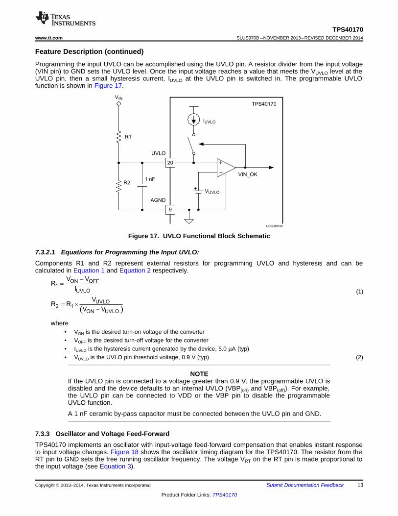
Feature Description (continued)Programming the input UVLO can be accomplished using the UVLO pin. A resistor divider from the input voltage(VIN pin) to GND sets the UVLO level. Once the input voltage reaches a value that meets the VUVLO level at theUVLO pin, then a small hysteresis current, IUVLO at the UVLO pin is switched in. The programmable UVLOfunction is shown in Figure 17.
Figure 17. UVLO Functional Block Schematic
7.3.2.1 Equations for Programming the Input UVLO:Components R1 and R2 represent external resistors for programming UVLO and hysteresis and can becalculated in Equation 1 and Equation 2 respectively.
(1)
where• VON is the desired turn-on voltage of the converter• VOFF is the desired turn-off voltage for the converter• IUVLO is the hysteresis current generated by the device, 5.0 µA (typ)• VUVLO is the UVLO pin threshold voltage, 0.9 V (typ) (2)
NOTEIf the UVLO pin is connected to a voltage greater than 0.9 V, the programmable UVLO isdisabled and the device defaults to an internal UVLO (VBP(on) and VBP(off)). For example,the UVLO pin can be connected to VDD or the VBP pin to disable the programmableUVLO function.
A 1 nF ceramic by-pass capacitor must be connected between the UVLO pin and GND.
7.3.3 Oscillator and Voltage Feed-ForwardTPS40170 implements an oscillator with input-voltage feed-forward compensation that enables instant responseto input voltage changes. Figure 18 shows the oscillator timing diagram for the TPS40170. The resistor from theRT pin to GND sets the free running oscillator frequency. The voltage VRT on the RT pin is made proportional tothe input voltage (see Equation 3).

( )( ) ( ) ( )( )
( ) ( ) ( ) ( )( )
+ ´ +=
´ - ´ -
DS2 LOADOUT min OUT min
SW max
DS1 DS2ON min IN max OUT min
V I R R
f
t V I R R
( )æ ö
= - Wç ÷ç ÷è ø
4
RT
SW
10R 2 k
f
UDG-09200
VCOMP
VIN
RAMP
Minimum OFF Time
VCLK
PWM
t – Time
=IN
RT
PWM
VV
K
14
TPS40170SLUS970B –NOVEMBER 2013–REVISED DECEMBER 2014 www.ti.com
Product Folder Links: TPS40170
Submit Documentation Feedback Copyright © 2013–2014, Texas Instruments Incorporated
Feature Description (continued)
where• KPWM = 15 (3)
The resistor at the RT pin sets the current in the RT pin. The proportional current charges an internal 100-pFoscillator capacitor. The ramp voltage on this capacitor is compared with the RT pin voltage, VRT. Once the rampvoltage reaches VRT, the oscillator capacitor is discharged. The ramp that is generated by the oscillator (which isproportional to the input voltage) acts as voltage feed-forward ramp to be used in the PWM comparator.
The time between the start of the discharging oscillator capacitor and the start of the next charging cycle is fixedat 170 ns (typical). During the fixed discharge time, the PWM output is maintained as OFF. This is the minimumOFF-time of the PWM output.
Figure 18. Feed-Forward Oscillator Timing Diagram
7.3.3.1 Calculating the Timing Resistance (RRT)
where• fSW is the switching frequency in kHz• RRT is the resistor connected from RT pin to GND in kΩ (4)
NOTEThe switching frequency can be adjusted between 100 kHz and 600 kHz. The maximumswitching frequency before skipping pulses is determined by the input voltage, outputvoltage, FET resistances, DCR of the inductor, and the minimum on time of theTPS40170. Use Equation 5 to determine the maximum switching frequency. For furtherdetails, please see application note SLYT293.
´
=
´
SC DS(on)HS
OC DS(on)LS
I RA
I R
´ ´= =
m
OC DS(on) OC DS(on)ILIM
ILIM
I R I RR
I 9.0 A
15
TPS40170www.ti.com SLUS970B –NOVEMBER 2013–REVISED DECEMBER 2014
Product Folder Links: TPS40170
Submit Documentation FeedbackCopyright © 2013–2014, Texas Instruments Incorporated
Feature Description (continued)where
• fSW(max) is the maximum switching frequency• VOUT(min) is the minimum output voltage• VIN(max) is the maximum input voltage• IOUT(min) is the minimum output current• RDS1 is the high-side FET resistance• RDS2 is the low-side FET resistance• and RLOAD is the inductor series resistance (5)
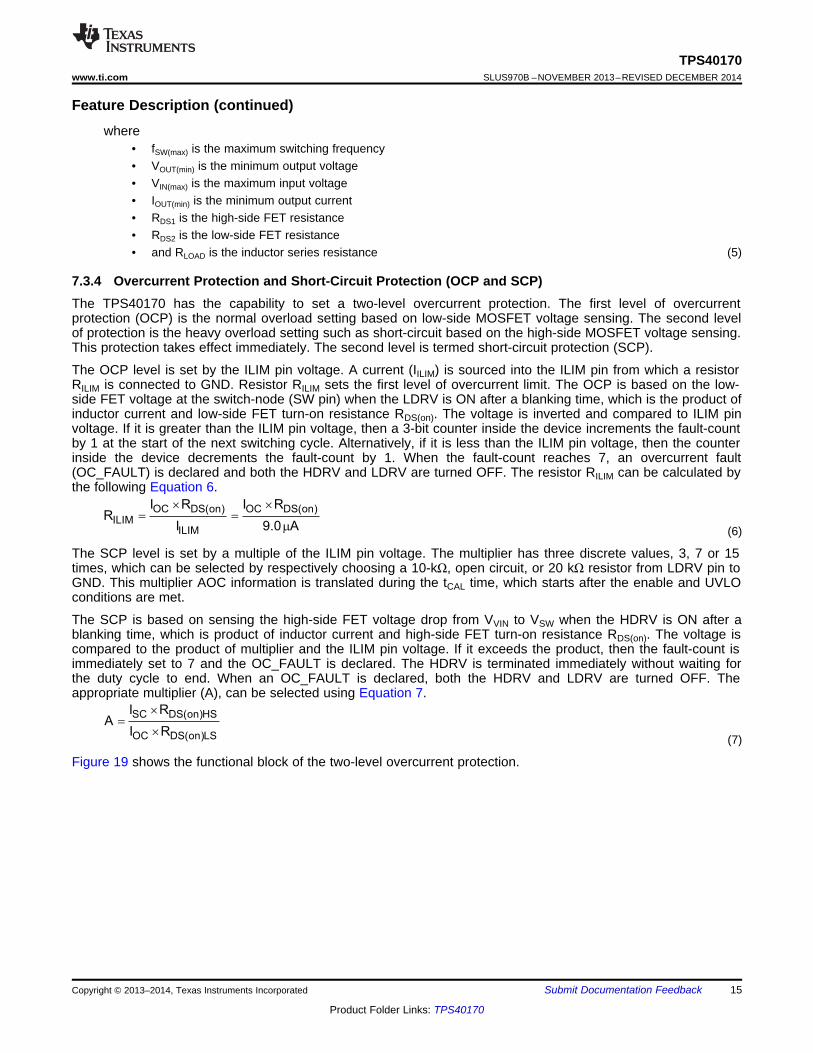
7.3.4 Overcurrent Protection and Short-Circuit Protection (OCP and SCP)The TPS40170 has the capability to set a two-level overcurrent protection. The first level of overcurrentprotection (OCP) is the normal overload setting based on low-side MOSFET voltage sensing. The second levelof protection is the heavy overload setting such as short-circuit based on the high-side MOSFET voltage sensing.This protection takes effect immediately. The second level is termed short-circuit protection (SCP).
The OCP level is set by the ILIM pin voltage. A current (IILIM) is sourced into the ILIM pin from which a resistorRILIM is connected to GND. Resistor RILIM sets the first level of overcurrent limit. The OCP is based on the low-side FET voltage at the switch-node (SW pin) when the LDRV is ON after a blanking time, which is the product ofinductor current and low-side FET turn-on resistance RDS(on). The voltage is inverted and compared to ILIM pinvoltage. If it is greater than the ILIM pin voltage, then a 3-bit counter inside the device increments the fault-countby 1 at the start of the next switching cycle. Alternatively, if it is less than the ILIM pin voltage, then the counterinside the device decrements the fault-count by 1. When the fault-count reaches 7, an overcurrent fault(OC_FAULT) is declared and both the HDRV and LDRV are turned OFF. The resistor RILIM can be calculated bythe following Equation 6.
(6)
The SCP level is set by a multiple of the ILIM pin voltage. The multiplier has three discrete values, 3, 7 or 15times, which can be selected by respectively choosing a 10-kΩ, open circuit, or 20 kΩ resistor from LDRV pin toGND. This multiplier AOC information is translated during the tCAL time, which starts after the enable and UVLOconditions are met.
The SCP is based on sensing the high-side FET voltage drop from VVIN to VSW when the HDRV is ON after ablanking time, which is product of inductor current and high-side FET turn-on resistance RDS(on). The voltage iscompared to the product of multiplier and the ILIM pin voltage. If it exceeds the product, then the fault-count isimmediately set to 7 and the OC_FAULT is declared. The HDRV is terminated immediately without waiting forthe duty cycle to end. When an OC_FAULT is declared, both the HDRV and LDRV are turned OFF. Theappropriate multiplier (A), can be selected using Equation 7.
(7)
Figure 19 shows the functional block of the two-level overcurrent protection.
19
17
16
14
13
12
RLDRV
VIN
HDRV
SW
LDRV
PGND
ILIM
RILIM
IILIM
VDD
R
+
R
+
+
tBLNK
LDRV On
+
tBLNK
HDRV On
3-Bit
State
Machine
Q0
Q1
Q2 CLK
(A x VILIM
)
OC_FAULT
RLDRV
(kW) A
10
OPEN
20
3
7
15
UDG-09198
16
TPS40170SLUS970B –NOVEMBER 2013–REVISED DECEMBER 2014 www.ti.com
Product Folder Links: TPS40170
Submit Documentation Feedback Copyright © 2013–2014, Texas Instruments Incorporated
Feature Description (continued)
Figure 19. OCP and SCP Protection Functional Block Diagram
NOTEBoth OCP and SCP are based on low-side and high-side MOSFET voltage sensing at theSW node. Excessive ringing on the SW node can have negative impact on the accuracy ofOCP and SCP. Adding an RC snubber from the SW node to GND helps minimize thepotential impact.
7.3.5 Soft-Start and Fault-LogicA capacitor from the SS pin to GND defines the SS time, tSS. The TPS40170 enters into soft-start immediatelyafter completion of the overcurrent calibration. The SS pin goes through the device's internal level-shifter circuitbefore reaching one of the positive inputs of the error amplifier. The SS pin must reach approximately 0.65 Vbefore the input to the error amplifier begins to rise above 0 V. To charge the SS pin from 0 V to 0.65 V faster, atthe beginning of the soft-start in addition to the normal charging current, (11.6 µA, typ.), an extra charging current(40.4 µA, typ.) is switched-in to the SS pin. As the SS capacitor reaches 0.5 V, the extra charging current isturned off and only the normal charging current remains. Figure 20 shows the soft-start function block.

5
7
SS
TPS40170
FB
UDG-09202
40.4 µA
R1
VDD
R2
+++
11.6 µA
VREF
FB
TRKSS Error Amplifier
COMP
CSS
VDD
VOUT
Soft-Start Charge/Discharge
Control1.05 µA
SS_EAmp
17
TPS40170www.ti.com SLUS970B –NOVEMBER 2013–REVISED DECEMBER 2014
Product Folder Links: TPS40170
Submit Documentation FeedbackCopyright © 2013–2014, Texas Instruments Incorporated
Feature Description (continued)
Figure 20. Soft-Start Schematic Block
As the SS pin voltage approaches 0.65 V, the positive input to the error amplifier begins to rise (see Figure 21).The output of the error amplifier (the COMP pin) starts rising. The rate of rise of the COMP voltage is mainlylimited by the feedback loop compensation network. Once VCOMP reaches the valley of the PWM ramp, theswitching begins. The output is regulated to the error amplifier input through the FB pin in the feedback loop.Once the FB pin reaches the 600 mV reference voltage, the feedback node is regulated to the reference voltage,VREF. The SS pin continues to rise and is clamped to VDD.
The SS pin is discharged through an internal switch during the following conditions:• Input (VIN) undervoltage lock out UVLO pin less than VUVLO• Overcurrent protection calibration time (tCAL)• VBP less than threshold voltage (VBP(off))
Because it is discharged through an internal switch, the discharging time is relatively fast compared with thedischarging time during the fault restart which is discussed in the Soft-Start During Overcurrent Fault section.

( )+= ´OUT REF
R1 R2V V
R2
( )+= ´OUT SS(EAMP)
R1 R2V V
R2
UDG-09203t – Time
Internal Logic RUN
Clamped at VDD
0.5 V VREF
= 0.6 V
SS
SS_EAMP
tSS
0.65 V
tCAL
1.1 V
VSS
VCOMP
VVALLEY
VOUT
(1)
(2)
18
TPS40170SLUS970B –NOVEMBER 2013–REVISED DECEMBER 2014 www.ti.com
Product Folder Links: TPS40170
Submit Documentation Feedback Copyright © 2013–2014, Texas Instruments Incorporated
Feature Description (continued)
Figure 21. Soft-Start Waveforms
NOTEReferring to Figure 21• (1) VREF dominates the positive input of the error amplifier• (2) SS_EAMP dominates the positive input of the error amplifier
For 0 < VSS_EAMP < VREF
(8)
For VSS_EAMP > VREF
(9)
7.3.5.1 Soft-Start During Overcurrent FaultThe soft-start block also has a role to controls the fault-logic timing. If an overcurrent fault (OC_FAULT) isdeclared, the soft-start capacitor is discharged internally through the device by a small current ISS(sink) (1.05 µA,typ.). Once the SS pin capacitor is discharged to below VSS(flt,low) (300 mV, typ.), the soft-start capacitor beginscharging again. If the fault is persistent, a fault is declared which is determined by the overcurrent protectionstate machine. If the soft-start capacitor is below VSS(flt,high) (2.5 V, typ.), then the soft-start capacitor continues tocharge until it reaches VSS(flt,high) before a discharge cycle is initiated. This ensures that the re-start time-intervalis always constant. Figure 22 shows the restart timing.

» ´RS SSt 2.28 C
=SS
SS
tC
0.09
UDG-09204t – Time
tRS
OC_FAULT
VSS
Persistent FAULT
FAULT SetFAULT Reset
2.5 V
300 mV
19
TPS40170www.ti.com SLUS970B –NOVEMBER 2013–REVISED DECEMBER 2014
Product Folder Links: TPS40170
Submit Documentation FeedbackCopyright © 2013–2014, Texas Instruments Incorporated
Feature Description (continued)
Figure 22. Overcurrent Fault Restart Timing
NOTEFor the feedback to be regulated to the SS_EAMP voltage, the TRK pin must be pulled uphigh directly or through a resistor to VDD.
7.3.5.2 Equations for Soft-Start and Restart TimeThe soft-start time (tSS) is defined as the time taken for the internal SS_EAMP node to go from 0 V to the 0.6 V,VREF voltage. The SS_EAMP starts rising as the SS pin goes beyond 0.65 V. The offset voltage between the SSand the SS_EAMP starts increasing as the SS pin voltage starts rising. Figure 21, shows that the SS time can bedefined as the time taken for the SS pin voltage to change by 1.05 V (see Equation 10).
The restart time (tRS) is defined in Equation 11 as the time taken for the soft-start capacitor (CSS) to dischargefrom 2.5 V to 0.3 V and to then recharge up to 2.5 V.
(10)
where• CSS is the soft-start capacitance in nF• tSS is the soft-start time in ms• tRS is the re-start time in ms (11)
NOTEDuring soft-start (VSS < 2.5 V), the overcurrent protection limit is 1.5 times normalovercurrent protection limit. This allows higher output capacitance to fully charge withoutactivating overcurrent protection.
7.3.6 Over-Temperature FaultFigure 23 shows the over-temperature protection scheme. If the junction temperature of the device reaches thethermal shutdown limit of tSD(set) (165°C, typ) and SS charging is completed, an over-temperature FAULT isdeclared. The soft-start capacitor begins to be discharged. During soft-start discharging period, the PWMswitching is terminated; therefore both HDRV and LDRV are driven low, turning off both MOSFETs.

UDG-09205t – Time
tRS
TS_FAULT
VSS
Persistent FAULT
FAULT SetFAULT Reset
2.5 V
300 mV
20
TPS40170SLUS970B –NOVEMBER 2013–REVISED DECEMBER 2014 www.ti.com
Product Folder Links: TPS40170
Submit Documentation Feedback Copyright © 2013–2014, Texas Instruments Incorporated
Feature Description (continued)The soft-start capacitor begins to charge and over-temperature fault is reset whenever the soft-start capacitor isdischarged below VSS(flt,low) (300 mV, typ.). During each restart cycle, PWM switching is turned on. When SS isfully charged, PWM switching is terminated. These restarts repeat until the temperature of the device has fallenbelow the thermal reset level, tSD(reset) (135°C typ). PWM switching continues and system returns to normalregulation.
Figure 23. Over-Temperature Fault Restart Timing
The soft-start timing during over-temperature fault is the same as the soft-start timing during overcurrent fault.See the Equations for Soft-Start and Restart Time section.
7.3.7 TrackingThe TRK pin is used for output voltage tracking. The output voltage is regulated so that the FB pin equals thelowest of the internal reference voltage (VREF) or the level-shifted SS pin voltage (SSEAMP) or the TRK pinvoltage. Once the TRK pin goes above the reference voltage, then the output voltage is no longer governed bythe TRK pin, but it is governed by the reference voltage.
If the voltage tracking function is used, then it should be noted that the SS pin capacitor must remain connectedas the SS pin and is also used for FAULT timing. For proper tracking using the TRK pin, the tracking voltageshould be allowed to rise only after SSEAMP has exceeded VREF, so that there is no possibility of the TRK pinvoltage being higher than the SSEAMP voltage. From Figure 21, for SSEAMP = 0.6 V, the SS pin voltage is typically1.7 V.
The maximum slew rate on the TRK pin should be determined by the output capacitance and feedback loopbandwidth. A higher slew rate can possibly trip overcurrent protection.
Figure 24 shows the tracking functional block. For SSEAMP voltages greater than TRK pin voltage, the VOUT isgiven by Equation 12 and Equation 13.

æ öæ ö æ ö= -ç ÷ç ÷ ç ÷ç ÷
è ø è øè ø
5 OUT2
6 OUT1
R V1
R V
( )æ ö+= ´ç ÷ç ÷
è ø
3 4
OUT2 REF
3
R RV V
R
( )æ ö+= ´ç ÷ç ÷
è ø
1 2
OUT1 REF
1
R RV V
R
( ) ( ) ( )
( )
æ öæ öç ÷ç ÷ç ÷+æ öæ ö ++ ç ÷è ø´ = ´ Þ = -ç ÷ç ÷ ç ÷ç ÷ ç ÷ æ öç ÷è ø è ø ç ÷ç ÷ç ÷+è øè ø
1
1 23 41 2 5TRK1 TRK2
1 3 6 3
3 4
R
R RR RR R RV V 1
R R R R
R R
7
TPS40170
FB
UDG-09208
R1
R2
+++
VREF
FB
COMP
VOUT
6
TRK
SSEAMP
TRK INTRK
( )+= ´OUT REF
R1 R2V V
R2
( )+= ´OUT TRK
R1 R2V V
R2
21
TPS40170www.ti.com SLUS970B –NOVEMBER 2013–REVISED DECEMBER 2014
Product Folder Links: TPS40170
Submit Documentation FeedbackCopyright © 2013–2014, Texas Instruments Incorporated
Feature Description (continued)
.For 0 V < VTRK < VREF
.
(12)
.For VTRK > VREF
.
(13)
Figure 24. Tracking Functional Block
There are three potential applications for the tracking function.• simultaneous voltage tracking• ratiometric voltage tracking• sequential startup mode
The tracking function configurations and waveforms are shown in Figure 25, Figure 27, and Figure 29respectively.
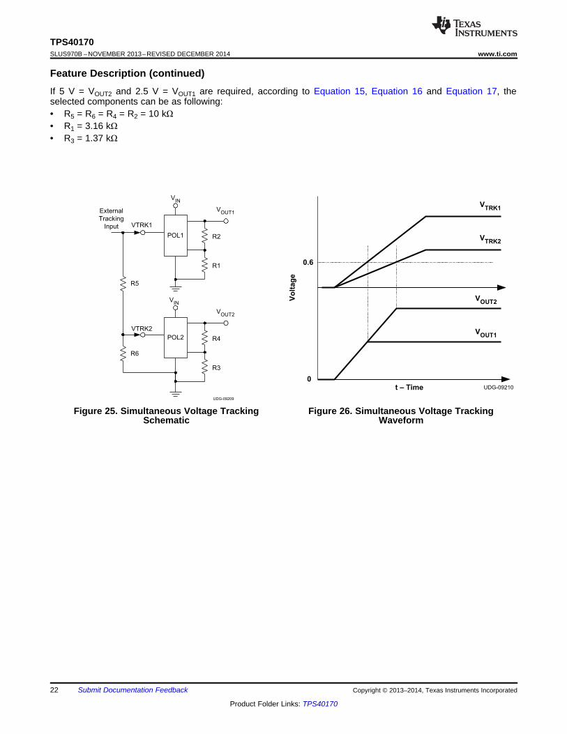
In simultaneous voltage tracking shown in Figure 25, tracking signals, VTRK1 and VTRK2, of two modules, POL1and POL2, start up at the same time and their output voltages VOUT1 initial and VOUT2 initial are approximately thesame during initial startup. Since VTRK1 and VTRK2 are less than VREF (0.6 V, typ), Equation 12 is used. As aresult, components selection should meet Equation 14.
(14)
After the lower output voltage setting reaches output voltage VOUT1 set point, where VTRK1 increases above VREF,the output voltage of the other one (VOUT2) continues increasing until it reaches its own set point, where VTRK2increases above VREF. At that time, Equation 13 is used. As a result, the resistor settings should meetEquation 15 and Equation 16.
(15)
(16)
Equation 14 can be simplified into Equation 17 by replacing with Equation 15 and Equation 16
(17)
UDG-09209
VTRK1
VIN
R2
VOUT1
R1
R5
External
Tracking
Input
VTRK2
VIN
R4
VOUT2
R3
R6
POL1
POL2
0
0.6
Vo
ltag
e
VTRK1
VTRK2
VOUT2
VOUT1
t – Time UDG-09210
22
TPS40170SLUS970B –NOVEMBER 2013–REVISED DECEMBER 2014 www.ti.com
Product Folder Links: TPS40170
Submit Documentation Feedback Copyright © 2013–2014, Texas Instruments Incorporated
Feature Description (continued)If 5 V = VOUT2 and 2.5 V = VOUT1 are required, according to Equation 15, Equation 16 and Equation 17, theselected components can be as following:• R5 = R6 = R4 = R2 = 10 kΩ• R1 = 3.16 kΩ• R3 = 1.37 kΩ
Figure 25. Simultaneous Voltage TrackingSchematic
Figure 26. Simultaneous Voltage TrackingWaveform
UDG-09211
VTRK1
VIN
R2
VOUT1
R1
External
Tracking
Input
VTRK2
VIN
R4
VOUT2
R3
POL1
POL2
0
0.6
Vo
ltag
e
VTRK1
VTRK2
VOUT2
VOUT1
t – Time UDG-09212
23
TPS40170www.ti.com SLUS970B –NOVEMBER 2013–REVISED DECEMBER 2014
Product Folder Links: TPS40170
Submit Documentation FeedbackCopyright © 2013–2014, Texas Instruments Incorporated
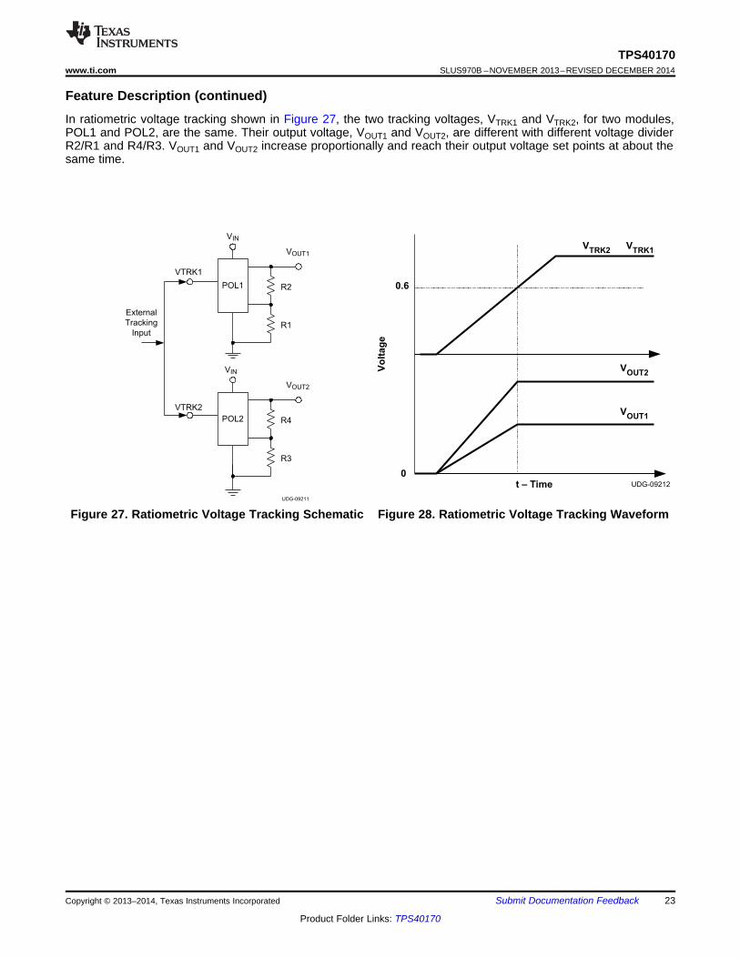
Feature Description (continued)In ratiometric voltage tracking shown in Figure 27, the two tracking voltages, VTRK1 and VTRK2, for two modules,POL1 and POL2, are the same. Their output voltage, VOUT1 and VOUT2, are different with different voltage dividerR2/R1 and R4/R3. VOUT1 and VOUT2 increase proportionally and reach their output voltage set points at about thesame time.
Figure 27. Ratiometric Voltage Tracking Schematic Figure 28. Ratiometric Voltage Tracking Waveform
UDG-09213
PGOOD1
VIN
R2
VOUT1
R1
SS2
VIN
R4
VOUT2
R3
POL1
POL2
CSS
0
Vo
ltag
e
VSS2
, VPGOOD1
VOUT1
VOUT2
VPGOOD2
t – Time UDG-09214
24
TPS40170SLUS970B –NOVEMBER 2013–REVISED DECEMBER 2014 www.ti.com
Product Folder Links: TPS40170
Submit Documentation Feedback Copyright © 2013–2014, Texas Instruments Incorporated
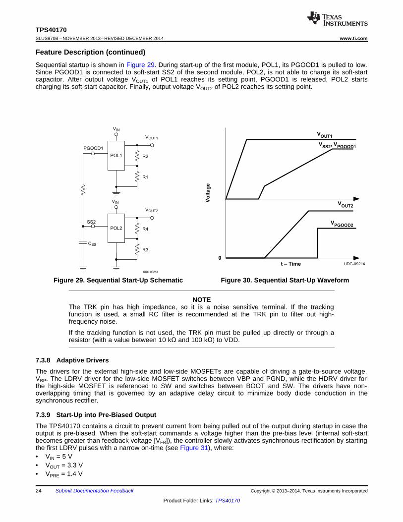
Feature Description (continued)Sequential startup is shown in Figure 29. During start-up of the first module, POL1, its PGOOD1 is pulled to low.Since PGOOD1 is connected to soft-start SS2 of the second module, POL2, is not able to charge its soft-startcapacitor. After output voltage VOUT1 of POL1 reaches its setting point, PGOOD1 is released. POL2 startscharging its soft-start capacitor. Finally, output voltage VOUT2 of POL2 reaches its setting point.
Figure 29. Sequential Start-Up Schematic Figure 30. Sequential Start-Up Waveform
NOTEThe TRK pin has high impedance, so it is a noise sensitive terminal. If the trackingfunction is used, a small RC filter is recommended at the TRK pin to filter out high-frequency noise.
If the tracking function is not used, the TRK pin must be pulled up directly or through aresistor (with a value between 10 kΩ and 100 kΩ) to VDD.
7.3.8 Adaptive DriversThe drivers for the external high-side and low-side MOSFETs are capable of driving a gate-to-source voltage,VBP. The LDRV driver for the low-side MOSFET switches between VBP and PGND, while the HDRV driver forthe high-side MOSFET is referenced to SW and switches between BOOT and SW. The drivers have non-overlapping timing that is governed by an adaptive delay circuit to minimize body diode conduction in thesynchronous rectifier.
7.3.9 Start-Up into Pre-Biased OutputThe TPS40170 contains a circuit to prevent current from being pulled out of the output during startup in case theoutput is pre-biased. When the soft-start commands a voltage higher than the pre-bias level (internal soft-startbecomes greater than feedback voltage [VFB]), the controller slowly activates synchronous rectification by startingthe first LDRV pulses with a narrow on-time (see Figure 31), where:• VIN = 5 V• VOUT = 3.3 V• VPRE = 1.4 V

25
TPS40170www.ti.com SLUS970B –NOVEMBER 2013–REVISED DECEMBER 2014
Product Folder Links: TPS40170
Submit Documentation FeedbackCopyright © 2013–2014, Texas Instruments Incorporated
Feature Description (continued)• fSW = 300 kHz• L = 0.6 µH
It then increments the on-time on a cycle-by-cycle basis until it coincides with the time dictated by (1-D), where Dis the duty cycle of the converter. This scheme prevents the initial sinking of the pre-bias output, and ensuresthat the output voltage (VOUT) starts and ramps up smoothly into regulation and the control loop is given time totransition from pre-biased startup to normal mode operation with minimal disturbance to the output voltage. Thetime from the start of switching until the low-side MOSFET is turned on for the full (1-D) interval is betweenapproximately 20 and 40 clock cycles.
Figure 31. Start-Up Switching Waveform during Pre-Biased Condition
If the output is pre-biased to a voltage higher than the voltage commanded by the reference, then the PWMswitching does not start.
NOTEWhen output is pre-biased at VPRE-BIAS, that voltage also applies to the SW node duringstart-up. When the pre-bias circuitry commands the first few high-side pulses before thefirst low-side pulse is initiated, the gate voltage for the high-side MOSFET is as describedin Equation 18. Alternatively, If pre-bias level is high, it is possible that SCP can be trippeddue to high turn-on resistance of the high-side MOSFET with low gate voltage. Oncetripped, the device resets and then attempts to re-start. The device may not be able tostart up until output is discharged to a lower voltage level by either an active load orthrough feedback resistors.
In the case of a high pre-bias level, a low gate-threshold voltage rated device isrecommended for the high-side MOSFET and increasing the SCP level also helpsalleviate the problem.

UDG-09215
tPGD
t – Time
VUV
VOV
VFB
VPGOOD
Track
VSS
VSS, FLT, HI
VSS, steady-state
VDD
( ) ( )-= - -BP DFWD PRE BIASGATE hsV V V V
26
TPS40170SLUS970B –NOVEMBER 2013–REVISED DECEMBER 2014 www.ti.com
Product Folder Links: TPS40170
Submit Documentation Feedback Copyright © 2013–2014, Texas Instruments Incorporated
Feature Description (continued)
where• VGATE(hs) is the gate voltage for the high-side MOSFET• VBP is the BP regulator output• VDFWD is bootstrap diode forward voltage (18)
7.3.10 Powergood (PGOOD)The TPS40170 provides an indication that the output voltage of the converter is within the specified limits of theregulation as measured at the FB pin. The PGOOD pin is an open-drain signal and pulls low when any conditionexists that would indicate that the output of the supply might be out of regulation. These conditions include:• VFB is not within the PGOOD threshold limits.• Soft-start is active, i.e., SS pin voltage is below VSS,FLT,HIGH limit.• An undervoltage condition exists for the device.• An overcurrent or short-circuit fault is detected.• An over-temperature fault is detected.
Figure 32 shows a situation where no fault is detected during the startup, (the normal PGOOD situation). Itshows that PGOOD goes high tPGD (20 µs, typ.) after all the conditions (listed above) are met.
Figure 32. PGOOD Signal
When there is no power to the device, PGOOD is not able to pull close to GND if an auxiliary supply is used forthe power good indication. In this case, a built-in resistor connected from drain to gate on the PGOOD pull-downdevice allows the PGOOD pin to operate like as a diode to GND.
7.3.11 PGND and AGNDTPS40170 provides separate signal ground (AGND) and power ground (PGND) pins. PGND is primarily used forgate driver ground return. AGND is an internal logic signal ground return. These two ground signals are internallyloosely connected by two anti-parallel diodes. PGND and AGND must be electrically connected externally.

t – Time
VHDRV
VSYNC
Master Mode (SYNC as an output pin)
t – Time
VHDRV
VSYNC
Slave 180 Mode (SYNC as an input pin)
t – Time
VHDRV
VSYNC
Slave 0 Mode (SYNC as an input pin)
UDG-09206
27
TPS40170www.ti.com SLUS970B –NOVEMBER 2013–REVISED DECEMBER 2014
Product Folder Links: TPS40170
Submit Documentation FeedbackCopyright © 2013–2014, Texas Instruments Incorporated
7.4 Device Functional Modes
7.4.1 Frequency SynchronizationThe TPS40170 has three modes.• Master mode: In this mode the master/slave selector pin, (M/S) is connected to VIN. The SYNC pin emits a
stream of pulses at the same frequency as the PWM switching frequency. The pulse stream at the SYNC pinis at 50% duty cycle and the same amplitude as VVBP. Also, the falling edge of the voltage on SYNC pin issynchronized with the rising edge of the HDRV.
• Slave-180° mode: In this mode the M/S pin is connected to GND. The SYNC pin of the TPS40170 accepts asynchronization clock signal, and the HDRV is synchronized with the rising edge of the incomingsynchronization clock.
• Slave-0° mode: In this mode, the M/S pin is left open. The SYNC pin of the TPS40170 accepts asynchronization clock signal, and the HDRV is synchronized with the falling edge of the incomingsynchronization clock.
The two slave modes can be synchronized to an external clock through the SYNC pin. They are shown inFigure 33. The synchronization frequency should be within ±30% of its programmed free running frequency.
Figure 33. Frequency Synchronization Waveforms In Different Modes

VHDRV
VSYNC
Synchronized duration 20-ms transition duration Free running duration .
fS
= SYNC clock frequency fS
= 0.7 x running frequency fS
= free running frequency
SYNC clock pulse missing
UDG-09207
28
TPS40170SLUS970B –NOVEMBER 2013–REVISED DECEMBER 2014 www.ti.com
Product Folder Links: TPS40170
Submit Documentation Feedback Copyright © 2013–2014, Texas Instruments Incorporated
Device Functional Modes (continued)TPS40170 provides a smooth transition for the SYNC clock signal loss at slave mode. In slave mode, asynchronization clock signal is provided externally through the SYNC pin to the device. The switching frequencyis synchronized to the external SYNC clock signal. If for some reason the external clock signal is missing, thedevice switching frequency is automatically overridden by a transition frequency which is 0.7 times itsprogrammed free running frequency. This transition time is approximately 20 μs. After that, the device switchingfrequency is changed to its programmed free running frequency. Figure 34 shows this process.
Figure 34. Transition for Sync Clock Signal Missing (For Slave-180 Mode)
NOTEWhen the device is operating in the master mode with duty ratio around 50%, PWMjittering may occur. Always configure the device into the slave mode by either connectingthe M/S pin to GND or leaving it floating if master mode is not used.
When an external SYNC clock signal is used for synchronization, limit maximum slew rateof the clock signal to 10 V/µs to avoid potential PWM jittering and connect the SYNC pinto the external clock signal via a 5-kΩ resistor.
7.4.2 Operation Near Minimum VIN (VVIN ≤ 4.5 V)The TPS40170 is designed to operate with input voltages above 4.5 V. With voltages below 4.5 V if the EN pin isabove its 600 mV turn on threshold the VDD and VBP internal regulators are active. These regulators willoperate in drop out and output the highest voltage possible for the given VIN. The EN pin voltage must be below100 mV to disable the VDD and VBP regulators. Switching is disabled while the VBP output voltage is below theVBP turn-on voltage of 4.4 V maximum. When there is sufficient VIN voltage to regulate the VBP voltage above4.4 V the final condition for switching to begin is the UVLO pin voltage must be above its 900 mV typicalthreshold. Once all three conditions are met the TPS40170 will begin switching and the soft-start sequence isinitiated. The device starts at the soft-start time determined by the external capacitance at the SS/TR pin. If adesign requires operation near the minimum VIN voltage, due to lower VBP voltage when operating in dropout,lower gate threshold MOSFETs are recommended

29
TPS40170www.ti.com SLUS970B –NOVEMBER 2013–REVISED DECEMBER 2014
Product Folder Links: TPS40170
Submit Documentation FeedbackCopyright © 2013–2014, Texas Instruments Incorporated
8 Application and Implementation
NOTEInformation in the following applications sections is not part of the TI componentspecification, and TI does not warrant its accuracy or completeness. TI’s customers areresponsible for determining suitability of components for their purposes. Customers shouldvalidate and test their design implementation to confirm system functionality.
8.1 Application InformationThe wide input TPS40170 controller can function in a very wide range of applications. The WEBENCH softwareuses an iterative design procedure and accesses a comprehensive database of components when generating adesign. This section presents a simplified discussion of the design process.
8.1.1 Bootstrap ResistorA small resistor in series with the bootstrap capacitor reduces the turn-on speed of the high-side MOSFET,thereby reducing the rising edge ringing of the SW node and reduces short through induced by dv/dt. A bootstrapresistor value that is too large delays the turn-on time of the high-side switch and may trigger an apparent SCPfault.
8.1.2 SW Node Snubber CapacitorObservable voltage ringing at the SW node is caused by fast switching edges and parasitic inductance andcapacitance. If the ringing results in excessive voltage on the SW node, or erratic operation of the converter, anRC snubber may be used to dampen the ringing and ensure proper operation over the full load range. Seedesign example.
8.1.3 Input ResistorThe TPS40170 has a wide input voltage range which allows for the device input to share power source withpower stage input. Power stage switching noise may pollute the device power source if the layout is notadequate in minimizing noise. It may trigger short-circuit fault. If so, adding a small resistor between the deviceinput and power stage input is recommended. This resistor composites an RC filter with the device inputcapacitor and filter out the switching noise from power stage. See R1 in the design example.
8.1.4 LDRV Gate CapacitorPower device selection is important for proper switching operation. If the low-side MOSFET has low gatecapacitance CGS (if CGS<CGD), there is a risk of short-through induced by high dv/dt at switching node (Seereference[1]) during high-side turned-on. If this happens, add a small capacitance between LDRV and GND. Seedesign example.

+
30
TPS40170SLUS970B –NOVEMBER 2013–REVISED DECEMBER 2014 www.ti.com
Product Folder Links: TPS40170
Submit Documentation Feedback Copyright © 2013–2014, Texas Instruments Incorporated
8.2 Typical ApplicationThis example describes the design process for a very wide input (10 V to 60 V) to a regulated 5 V output at aload current of 6 A. The schematic shown in Figure 35 is configured for the design parameters provided inTable 1. Alternatively the WEBENCH software can be used to generate a complete design with the TPS40170.
Figure 35. Typical Design Application
8.2.1 Design Requirements
Table 1. Design RequirementsPARAMETER TEST CONDITIONS MIN NOM MAX UNIT
VIN Input voltage 10 60VVIN(ripple) Input ripple IOUT = 6 A 0.5
VOUT Output voltage 0 A ≤ IOUT ≤ 20 A 4.8 5.0 5.2Line regulation 10 V ≤ VIN ≤ 60 V 0.5%Load regulation 0 A ≤ IOUT ≤ 6 A 0.5%
VRIPPLE Output ripple IOUT = 6 A 100mVVOVER Output overshoot ΔIOUT = 2.5 A 250
VUNDER Output undershoot ΔIOUT = -2.5 A 250IOUT Output current 10 V ≤ VIN ≤ 60 V 0 6 AtSS Soft-start time VIN = 24 V 4 msISCP Short circuit current trip point 8 Aη Efficiency VIN = 24 V, IOUT = 6 A 94%fSW Switching frequency 300 kHz
Size 1.5 in2

31
TPS40170www.ti.com SLUS970B –NOVEMBER 2013–REVISED DECEMBER 2014
Product Folder Links: TPS40170
Submit Documentation FeedbackCopyright © 2013–2014, Texas Instruments Incorporated
8.2.2 Detailed Design Procedure
8.2.2.1 Custom Design with WEBENCH ToolsClick here to create a custom design using the TPS40170 device with the WEBENCH® Power Designer.1. Start by entering your VIN, VOUT and IOUT requirements.2. Optimize your design for key parameters like efficiency, footprint and cost using the optimizer dial and
compare this design with other possible solutions from Texas Instruments.3. WEBENCH Power Designer provides you with a customized schematic along with a list of materials with real
time pricing and component availability.4. In most cases, you will also be able to:
– Run electrical simulations to see important waveforms and circuit performance,– Run thermal simulations to understand the thermal performance of your board,– Export your customized schematic and layout into popular CAD formats,– Print PDF reports for the design, and share your design with colleagues.
5. Get more information about WEBENCH tools at www.ti.com/webench.
8.2.2.2 List of Materials
Table 2. Design Example List of MaterialsREFERENCEDESIGNATOR QTY VALUE DESCRIPTION SIZE PART NUMBER MANUF
C1 4 2.2 µF Capacitor, Ceramic, 100 V, X7R, 15% 1210 Std Std
C6 1 120 µF Capacitor, Aluminum, 63 V, 20%, KZESeries 0.315" KZE63VB121M10X16LL Chemi-con
C7 1 0.1 µF Capacitor, Ceramic, 50 V, X7R, 15% 603 Std Std
C9 2 ea 22 µF10 µF Capacitor, Ceramic, 16 V, X7R, 15% 1210 Std Std
C13 1 8200 pF Capacitor, Ceramic, 50 V, X7R, 15% 603 Std StdC14 1 220 pF Capacitor, Ceramic, 50 V, X7R, 15% 603 Std StdC15 1 47 nF Capacitor, Ceramic, 50 V, X7R, 15% 603 Std StdC16 1 1 µF Capacitor, 1 6V, X7R, 15% 603 Std StdC17 1 1000 pF Capacitor, Ceramic, 50 V, X7R, 15% 603 Std StdC18 1 1 µF Capacitor, Ceramic, 100 V, X7R, 15% 1206 Std StdC19 1 4.7 µF Capacitor, Ceramic, 16 V, X5R, 15% 805 Std StdC21 1 1500 pF Capacitor, Ceramic, 50 V, X7R, 15% 603 Std StdL1 1 8.2 µH Inductor, SMT, 10 A, 16 mΩ 0.51"2 IHLP5050FDER8R2M01 VishayQ1 1 MOSFET, N-channel, 60 V, 50 A, 11 mΩ BSC110N06NS3G InfineonQ2 1 MOSFET, N-channel, 60 V, 50 A, 7.6 mΩ BSC076N06NS3G InfineonR10 1 2.74 kΩ Resistor, Chip, 1/16W, 1% 603 Std R603R4 1 3.83 kΩ Resistor, Chip, 1/16W, 1% 603 Std R603R5 1 10.0 kΩ Resistor, Chip, 1/16W, 1% 603 Std R603R9 1 12.1 kΩ Resistor, Chip, 1/16W, 1% 603 Std R603R11 1 20.0 kΩ Resistor, Chip, 1/16W, 1% 603 Std R603R6 1 22.1 kΩ Resistor, Chip, 1/16W, 1% 603 Std R603R7 1 31.6 kΩ Resistor, Chip, 1/16W, 1% 603 Std R603R2 1 200 kΩ Resistor, Chip, 1/16W, 1% 603 Std R603R13 1 511 kΩ Resistor, Chip, 1/16W, 1% 603 Std R603
U1 IC, 4.5 V - 60 V wide input sync. PWMbuck controller TPS40170RGY Texas
Instruments

( ) ( )= + ´ + = + ´ + =1 1OUT(max) RIPPLE CHARGEL peak 2 2I I I I 6 A 1.86 A 0.08 A 7.01A
( )´ ´ m + ´ m´= = =OUT OUT
CHARGE
SS
5 V 2 22 F 2 10 FV CI 0.08 A
t 4ms
æ ö æ ö- -ç ÷ ç ÷- ´ ´ ´ m ´è ø è ø= = = = W
RIPPLERIPPLE(tot)
RIPPLE(tot) RIPPLE(cap) OUT SWMAX
RIPPLE RIPPLE
I 1.86 AV 100mV
V V 8 C f 8 59 F 300kHzESR 47m
I I 1.86 A
( )( ) ( )´ ´ m
= = = m´ ´
2 2TRAN(max)
OUT minOUT OVER
I L 3 8.2 HC 59 F
V V 5 250mV
( )( )
( )
´´< ´ D = ´ =
- - ´
2
TRANTRAN TRAN TRANUNDER
OUT OUT IN OUT IN OUT OUT
I LI I I LV T
C C V V V V C
( ) ´´< ´ D = ´ =
´
2
TRANTRAN TRAN TRANOVER
OUT OUT OUT OUT OUT
I LI I I LV T
C C V V C
( ) ( )( ) ( ) ( ) ( ) ( ) ( )= + ´ = + ´ = + ´ =2 22 2 2 21 1 1
RIPPLE OUT RIPPLEL rms L avg 12 12 12I I I I I 6 1.86 6.02A
( )
( )
- -» ´ ´ = ´ ´ = m
´ ´
OUTIN max OUT
OUT SWIN max
V V V 1 60 V 5 V 5 V 1L 8.5 H
0.3 I V f 0.3 6 A 60 V 300kHz
32
TPS40170SLUS970B –NOVEMBER 2013–REVISED DECEMBER 2014 www.ti.com
Product Folder Links: TPS40170
Submit Documentation Feedback Copyright © 2013–2014, Texas Instruments Incorporated
8.2.2.3 Select a Switching FrequencyTo maintain acceptable efficiency and meet minimum on-time requirements, a 300 kHz switching frequency isselected.
8.2.2.4 Inductor Selection (L1)Synchronous buck power inductors are typically sized for approximately 20-40% peak-to-peak ripple current(IRIPPLE) Given this target ripple current, the required inductor size can be calculated in Equation 19.
(19)
Selecting a standard 8.2 µH inductor value, solving for IRIPPLE = 1.86 A.
The RMS current through the inductor is approximated by Equation 20.
(20)
8.2.2.5 Output Capacitor Selection (C9)The selection of the output capacitor is typically driven by the output transient response. The Equation 21 andEquation 22 overestimate the voltage deviation to account for delays in the loop bandwidth and can be used todetermine the required output capacitance:
(21)
(22)
If VIN(min) > 2 x VOUT, use overshoot to calculate minimum output capacitance. If VIN(min) < 2 x VOUT, useundershoot to calculate minimum output capacitance.
(23)
With a minimum capacitance, the maximum allowable ESR is determined by the maximum ripple voltage and isapproximated Equation 24.
(24)
Two 1210, 22 µF, 16 V X7R ceramic capacitors plus two 0805 10 µF, 16 V X7R ceramic capacitors are selectedto provide more than 59 µF of minimum capacitance (including tolerance and DC bias derating) and less than47 mΩ of ESR (parallel ESR of approximately 4 mΩ).
8.2.2.6 Peak Current Rating of InductorWith output capacitance, it is possible to calculate the charge current during start-up and determine the minimumsaturation current rating for the inductor. The start-up charging current is approximated in Equation 25.
(25)
(26)
An IHLP5050FDER8R2M01 8.2 µH is selected. This 10-A, 16-mΩ inductor exceeds the minimum inductor ratingsin a 13 mm × 13 mm package.
( ) ( )= - W = - = W » W
4 4
RT
SW
10 10R 2k 2 31.3k 31.6k
f 300kHz
( )- æ ö´= + ´ ´ç ÷
è ø
9 FD OUT GDRIVE SW
DRIVE SW
V I QWJ 10 V f
nCI Q
( ) ( ) ( )( ) ( )--
æ ö= + ´ ´ -ç ÷ Wè ø
23 2 OUT1OUT P P12
IN
VWK 10 I I 1
mV
( ) ( ) ( )( ) ( )--
æ ö= + ´ ´ ç ÷ Wè ø
23 2 OUT1OUT P P12
IN
VWK 10 I I
mV
( ) ( )- æ ö´= ´ + ´ ´ç ÷
è ø
9 IN OUT GDRIVE SW
DRIVE SW
V I QWJ 10 V f
nCI Q
( ) ( )= ´ ´ - = ´ ´ - =LOADRMS cinI I D 1 D 6 A 0.5 (1 0.5) 3.0 A
= = = W+ ´
RIPPLE(esr)MAX 1
LOAD RIPPLE2
V 100mVESR 14.4m
I I 6.93A
´ ´= = = m
´ ´ ´ ´
LOAD OUTIN(min)
RIPPLE(cap) IN SW
I V 6 A 5 VC 25 F
V V f 400mV 10 V 300kHz
33
TPS40170www.ti.com SLUS970B –NOVEMBER 2013–REVISED DECEMBER 2014
Product Folder Links: TPS40170
Submit Documentation FeedbackCopyright © 2013–2014, Texas Instruments Incorporated
8.2.2.7 Input Capacitor Selection (C1, C6)The input voltage ripple is divided between capacitance and ESR. For this design VRIPPLE(cap) = 400 mV andVRIPPLE(ESR) = 100 mV. The minimum capacitance and maximum ESR are estimated by:
(27)
(28)
The RMS current in the input capacitors is estimated in Equation 29.
(29)
To achieve these values, four 1210, 2.2 µF, 100 V, X7R ceramic capacitors plus a 120 µF electrolytic capacitorare combined at the input. This provides a smaller size and overall cost than 10 ceramic input capacitors or anelectrolytic capacitor with the ESR required.
Table 3. Inductor SummaryPARAMETER VALUE UNIT
L Inductance 8.2 µHIL(rms) RMS current (thermal rating) 6.02 AIL(peak) Peak current (saturation rating) 7.01 A
8.2.2.8 MOSFET Switch Selection (Q1, Q2)Using the J/K method for MOSFET optimization, apply Equation 30 through Equation 33.
High-side gate (Q1):
(30)
(31)
Low-side gate (Q2):
(32)
(33)
Optimizing for 300 kHz, 24 V input, 5 V output at 6 A, calculate ratios of 5.9 mΩ/nC and 0.5 mΩ/nC for the high-side and low-side FETS respectively. BSC110N06NS2 (Ratio 1.2) and BSC076N06NS3 (Ratio 0.69) MOSFETSare selected.
8.2.2.9 Timing Resistor (R7)The switching frequency is programmed by the current through RRT to GND. The RRT value is calculated usingEquation 34.
(34)
8.2.2.10 UVLO Programming Resistors (R2, R6)The UVLO hysteresis level is programmed by R2 using Equation 35.
( )= = = W » W
m
OCILIM
OCSET min
V 107.6mVR 12.0k 12.1k
I 9.0 A
( ) ( )( ) ( )= ´ + ´ ´ ´ = ´ + ´ ´ ´ W =1 1OC OCP(min) RIPPLE DS on G22 2
V 1.3 I I 1.25 R (1.3 8 A 1.86 A) 1.25 7.6m 107.6mV
= = = »SS
SS
t 4msC 44nF 47nF
0.09 0.09
( )= = =G1
BOOSTBOOT ripple
Q 25nCC 100nF
V 250mV
( ) ( ) ( ) ( )> = W = W » W
--
UVLO(max)UVLO set UVLO hys
UVLO _ ON(min) UVLO(max)
V 0.919 VR R 200k 22.7k 22.1k
9.0 V 0.919 VV V
( )( ) ( )- -
= = = Wm
UVLO on UVLO off
UVLO hysUVLO
V V 9 V 8 VR 200k
I 5.0 A
34
TPS40170SLUS970B –NOVEMBER 2013–REVISED DECEMBER 2014 www.ti.com
Product Folder Links: TPS40170
Submit Documentation Feedback Copyright © 2013–2014, Texas Instruments Incorporated
(35)
(36)
8.2.2.11 Boot-Strap Capacitor (C7)A bootstrap capacitor with a value between 0.1 µF and 0.22 µF must be placed between the BOOT pin and theSW pin. It should be 10 times higher than MOSFET gate capacitance. To ensure proper charging of the high-side FET gate, limit the ripple voltage on the boost capacitor to less than 250 mV.
(37)
8.2.2.12 VIN Bypass Capacitor (C18)Place a capacitor with a value of 1.0 µF. Select a capacitor with a value from 0.1 µF to 1.0 µF, X5R or betterceramic bypass capacitor for VIN as specified in Recommended Operating Conditions. For this design a 1.0-µF,100-V, X7R capacitor has been selected.
8.2.2.13 VBP Bypass Capacitor (C19)Select a capacitor with a value from 1.0 µF to 10 µF, X5R or better ceramic bypass capacitor for VBP asspecified in Recommended Operating Conditions. It should be at least 10 times higher than the bootstrapcapacitance. For this design a 4.7-µF, 16-V capacitor has been selected.
8.2.2.14 VDD Bypass Capacitor (C16)Select a capacitor with a value between 0.1 µF and 1 µF, X5R or better ceramic bypass capacitor for VDD asspecified in Recommended Operating Conditions. For this design a 1-µF, 16-V capacitor has been selected.
8.2.2.15 SS Timing Capacitor (C15)The soft-start capacitor provides smooth ramp of the error amplifier reference voltage for controlled start-up. Thesoft-start capacitor is selected by using Equation 38.
(38)
8.2.2.16 ILIM Resistor (R9, C17)The TPS40170 use the negative drop across the low-side FET at the end of the "OFF" time to measure theinductor current. Allowing for 30% over the minimum current limit for transient recovery and 20% rise in RDS(on)Q2for self-heating of the MOSFET, the voltage drop across the low-side FET at current limit is given byEquation 39.
(39)
The internal current limit temperature coefficient helps compensate for the MOSFET RDS(on) temperaturecoefficient, so the current limit programming resistor is selected by Equation 40.
(40)
A 1000 pF capacitor is placed in parallel to improve noise immunity of the current limit set-point.
8.2.2.17 SCP Multiplier Selection (R5)The TPS40170 controller uses a multiplier (AOC) to translate the low-side over-current protection into a high-sideRDS(on) pulse-by-pulse short circuit protection. Ensure that Equation 41 is true.

70
75
80
85
90
95
100
0 1 2 3 4 5 6
Load Current (A)
Effic
iency (
%)
VIN = 10 V
VIN = 12 V
VIN = 24 V
VIN = 36 V
VIN = 48 V
VIN = 60 V0.1 1 10 100 1000
−60
−40
−20
0
20
40
60
80
100
−135
−90
−45
0
45
90
135
180
225
Frequency (kHz)
Gai
n (d
B)
Pha
se (
°)GainPhase
( ) ( )´ ´ W
= = = W » W--
FB
OUT FB
V R11 0.600 V 20.0kR10 2.73k 2.74k
5.0 V 0.600 VV V
( )( )
( )
( )
+ ´ + ´ W> ´ = ´ =
W+ ´+ ´
1 1OCP(min) RIPPLE DS on Q12 2
OC 11DS on Q2OCP(min) RIPPLE 22
RI I 8 A 1.86 A 11mA 1.45
R 7.6 m8 A 1.86 AI I
35
TPS40170www.ti.com SLUS970B –NOVEMBER 2013–REVISED DECEMBER 2014
Product Folder Links: TPS40170
Submit Documentation FeedbackCopyright © 2013–2014, Texas Instruments Incorporated
(41)
AOC = 3 is selected as the next greater AOC. The value of R5 is set to 10 kΩ.
8.2.2.18 Feedback Divider (R10, R11)The TPS40170 controller uses a full operational amplifier with an internally fixed 0.6 V reference. The value ofR11 is selected between 10 kΩ and 50 kΩ for a balance of feedback current and noise immunity. With the valueof R11 set to 20 kΩ, the output voltage is programmed with a resistor divider given by Equation 42.
(42)
8.2.2.19 Compensation: (R4, R13, C13, C14, C21)Using the TPS40k Loop Stability Tool for a 60 kHz bandwidth and a 50° phase margin with an R11 value of20.0 kΩ, the following values are obtained. The tool is available from the TI website, SLUC263.• C21 = C1 = 1500 pF• C13 = C2 = 8200 pF• C14 = C3 = 220 pF• R13 = R2 = 511 Ω• R4 = R3 = 3.83 kΩ
8.2.3 Application CurvesFigure 36 shows an input from 10 V to 60 V for an output of 5.0 V at 6 A, efficiency graph for this design.Figure 37 shows an input of 24 V for an output of 5.0 V at 6 A, loop response where VIN = 24V and IOUT = 6A,yielding 58 kHz bandwidth, 51° phase margin. Figure 38 shows the output ripple 20 mV/div, 2 µs/div, 20 MHzbandwidth.
Figure 36. Efficiency vs. Load Current Figure 37. Loop Response

36
TPS40170SLUS970B –NOVEMBER 2013–REVISED DECEMBER 2014 www.ti.com
Product Folder Links: TPS40170
Submit Documentation Feedback Copyright © 2013–2014, Texas Instruments Incorporated
Figure 38. Output Ripple Waveform
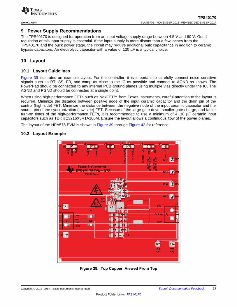
37
TPS40170www.ti.com SLUS970B –NOVEMBER 2013–REVISED DECEMBER 2014
Product Folder Links: TPS40170
Submit Documentation FeedbackCopyright © 2013–2014, Texas Instruments Incorporated
9 Power Supply RecommendationsThe TPS40170 is designed for operation from an input voltage supply range between 4.5 V and 60 V. Goodregulation of this input supply is essential. If the input supply is more distant than a few inches from theTPS40170 and the buck power stage, the circuit may require additional bulk capacitance in addition to ceramicbypass capacitors. An electrolytic capacitor with a value of 120 µF is a typical choice.
10 Layout
10.1 Layout GuidelinesFigure 39 illustrates an example layout. For the controller, it is important to carefully connect noise sensitivesignals such as RT, SS, FB, and comp as close to the IC as possible and connect to AGND as shown. ThePowerPad should be connected to any internal PCB ground planes using multiple vias directly under the IC. TheAGND and PGND should be connected at a single point.
When using high-performance FETs such as NexFET™ from Texas Instruments, careful attention to the layout isrequired. Minimize the distance between positive node of the input ceramic capacitor and the drain pin of thecontrol (high-side) FET. Minimize the distance between the negative node of the input ceramic capacitor and thesource pin of the syncronization (low-side) FET. Becasue of the large gate drive, smaller gate charge, and fasterturn-on times of the high-performance FETs, it is recommended to use a minimum of 4, 10 µF ceramic inputcapacitors such as TDK #C3216X5R1A106M. Ensure the layout allows a continuous flow of the power planes.
The layout of the HPA578 EVM is shown in Figure 39 through Figure 42 for reference.
10.2 Layout Example
Figure 39. Top Copper, Viewed From Top
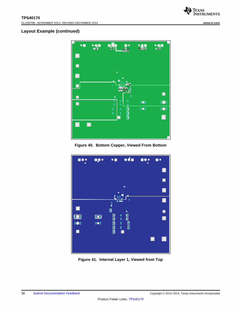
38
TPS40170SLUS970B –NOVEMBER 2013–REVISED DECEMBER 2014 www.ti.com
Product Folder Links: TPS40170
Submit Documentation Feedback Copyright © 2013–2014, Texas Instruments Incorporated
Layout Example (continued)
Figure 40. Bottom Copper, Viewed From Bottom
Figure 41. Internal Layer 1, Viewed from Top
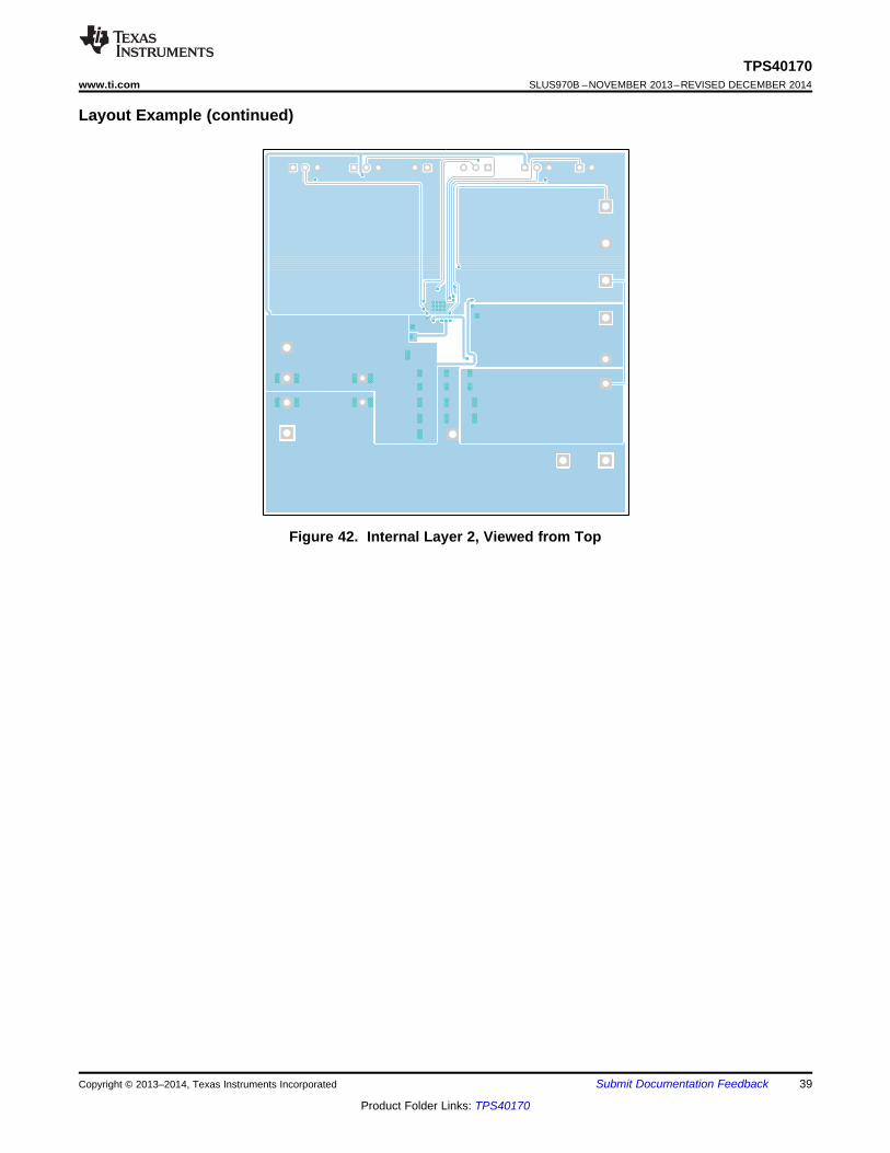
39
TPS40170www.ti.com SLUS970B –NOVEMBER 2013–REVISED DECEMBER 2014
Product Folder Links: TPS40170
Submit Documentation FeedbackCopyright © 2013–2014, Texas Instruments Incorporated
Layout Example (continued)
Figure 42. Internal Layer 2, Viewed from Top
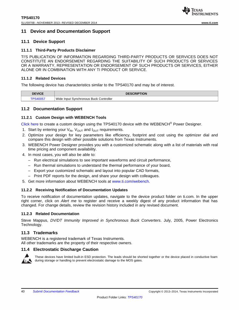
40
TPS40170SLUS970B –NOVEMBER 2013–REVISED DECEMBER 2014 www.ti.com
Product Folder Links: TPS40170
Submit Documentation Feedback Copyright © 2013–2014, Texas Instruments Incorporated
11 Device and Documentation Support
11.1 Device Support
11.1.1 Third-Party Products DisclaimerTI'S PUBLICATION OF INFORMATION REGARDING THIRD-PARTY PRODUCTS OR SERVICES DOES NOTCONSTITUTE AN ENDORSEMENT REGARDING THE SUITABILITY OF SUCH PRODUCTS OR SERVICESOR A WARRANTY, REPRESENTATION OR ENDORSEMENT OF SUCH PRODUCTS OR SERVICES, EITHERALONE OR IN COMBINATION WITH ANY TI PRODUCT OR SERVICE.
11.1.2 Related DevicesThe following device has characteristics similar to the TPS40170 and may be of interest.
DEVICE DESCRIPTIONTPS40057 Wide Input Synchronous Buck Controller
11.2 Documentation Support
11.2.1 Custom Design with WEBENCH ToolsClick here to create a custom design using the TPS40170 device with the WEBENCH® Power Designer.1. Start by entering your VIN, VOUT and IOUT requirements.2. Optimize your design for key parameters like efficiency, footprint and cost using the optimizer dial and
compare this design with other possible solutions from Texas Instruments.3. WEBENCH Power Designer provides you with a customized schematic along with a list of materials with real
time pricing and component availability.4. In most cases, you will also be able to:
– Run electrical simulations to see important waveforms and circuit performance,– Run thermal simulations to understand the thermal performance of your board,– Export your customized schematic and layout into popular CAD formats,– Print PDF reports for the design, and share your design with colleagues.
5. Get more information about WEBENCH tools at www.ti.com/webench.
11.2.2 Receiving Notification of Documentation UpdatesTo receive notification of documentation updates, navigate to the device product folder on ti.com. In the upperright corner, click on Alert me to register and receive a weekly digest of any product information that haschanged. For change details, review the revision history included in any revised document.
11.2.3 Related DocumentationSteve Mappus, DV/DT Immunity Improved in Synchronous Buck Converters. July, 2005, Power ElectronicsTechnology.
11.3 TrademarksWEBENCH is a registered trademark of Texas Instruments.All other trademarks are the property of their respective owners.
11.4 Electrostatic Discharge CautionThese devices have limited built-in ESD protection. The leads should be shorted together or the device placed in conductive foamduring storage or handling to prevent electrostatic damage to the MOS gates.
41
TPS40170www.ti.com SLUS970B –NOVEMBER 2013–REVISED DECEMBER 2014
Product Folder Links: TPS40170
Submit Documentation FeedbackCopyright © 2013–2014, Texas Instruments Incorporated
11.5 GlossarySLYZ022 — TI Glossary.
This glossary lists and explains terms, acronyms, and definitions.
12 Mechanical, Packaging, and Orderable InformationThe following pages include mechanical, packaging, and orderable information. This information is the mostcurrent data available for the designated devices. This data is subject to change without notice and revision ofthis document. For browser-based versions of this data sheet, refer to the left-hand navigation.
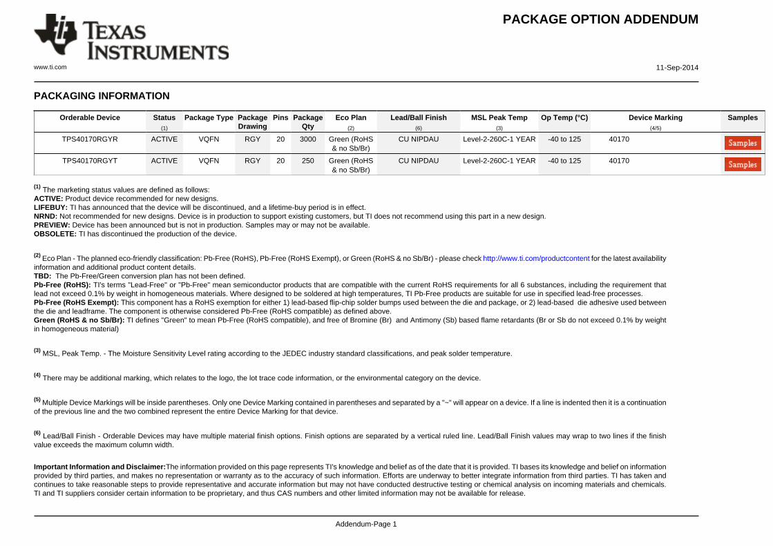
PACKAGE OPTION ADDENDUM
www.ti.com 11-Sep-2014
Addendum-Page 1
PACKAGING INFORMATION
Orderable Device Status(1)
Package Type PackageDrawing
Pins PackageQty
Eco Plan(2)
Lead/Ball Finish(6)
MSL Peak Temp(3)
Op Temp (°C) Device Marking(4/5)
Samples
TPS40170RGYR ACTIVE VQFN RGY 20 3000 Green (RoHS& no Sb/Br)
CU NIPDAU Level-2-260C-1 YEAR -40 to 125 40170
TPS40170RGYT ACTIVE VQFN RGY 20 250 Green (RoHS& no Sb/Br)
CU NIPDAU Level-2-260C-1 YEAR -40 to 125 40170
(1) The marketing status values are defined as follows:ACTIVE: Product device recommended for new designs.LIFEBUY: TI has announced that the device will be discontinued, and a lifetime-buy period is in effect.NRND: Not recommended for new designs. Device is in production to support existing customers, but TI does not recommend using this part in a new design.PREVIEW: Device has been announced but is not in production. Samples may or may not be available.OBSOLETE: TI has discontinued the production of the device.
(2) Eco Plan - The planned eco-friendly classification: Pb-Free (RoHS), Pb-Free (RoHS Exempt), or Green (RoHS & no Sb/Br) - please check http://www.ti.com/productcontent for the latest availabilityinformation and additional product content details.TBD: The Pb-Free/Green conversion plan has not been defined.Pb-Free (RoHS): TI's terms "Lead-Free" or "Pb-Free" mean semiconductor products that are compatible with the current RoHS requirements for all 6 substances, including the requirement thatlead not exceed 0.1% by weight in homogeneous materials. Where designed to be soldered at high temperatures, TI Pb-Free products are suitable for use in specified lead-free processes.Pb-Free (RoHS Exempt): This component has a RoHS exemption for either 1) lead-based flip-chip solder bumps used between the die and package, or 2) lead-based die adhesive used betweenthe die and leadframe. The component is otherwise considered Pb-Free (RoHS compatible) as defined above.Green (RoHS & no Sb/Br): TI defines "Green" to mean Pb-Free (RoHS compatible), and free of Bromine (Br) and Antimony (Sb) based flame retardants (Br or Sb do not exceed 0.1% by weightin homogeneous material)
(3) MSL, Peak Temp. - The Moisture Sensitivity Level rating according to the JEDEC industry standard classifications, and peak solder temperature.
(4) There may be additional marking, which relates to the logo, the lot trace code information, or the environmental category on the device.
(5) Multiple Device Markings will be inside parentheses. Only one Device Marking contained in parentheses and separated by a "~" will appear on a device. If a line is indented then it is a continuationof the previous line and the two combined represent the entire Device Marking for that device.
(6) Lead/Ball Finish - Orderable Devices may have multiple material finish options. Finish options are separated by a vertical ruled line. Lead/Ball Finish values may wrap to two lines if the finishvalue exceeds the maximum column width.
Important Information and Disclaimer:The information provided on this page represents TI's knowledge and belief as of the date that it is provided. TI bases its knowledge and belief on informationprovided by third parties, and makes no representation or warranty as to the accuracy of such information. Efforts are underway to better integrate information from third parties. TI has taken andcontinues to take reasonable steps to provide representative and accurate information but may not have conducted destructive testing or chemical analysis on incoming materials and chemicals.TI and TI suppliers consider certain information to be proprietary, and thus CAS numbers and other limited information may not be available for release.
PACKAGE OPTION ADDENDUM
www.ti.com 11-Sep-2014
Addendum-Page 2
In no event shall TI's liability arising out of such information exceed the total purchase price of the TI part(s) at issue in this document sold by TI to Customer on an annual basis.
OTHER QUALIFIED VERSIONS OF TPS40170 :
• Automotive: TPS40170-Q1
• Enhanced Product: TPS40170-EP
NOTE: Qualified Version Definitions:
• Automotive - Q100 devices qualified for high-reliability automotive applications targeting zero defects
• Enhanced Product - Supports Defense, Aerospace and Medical Applications
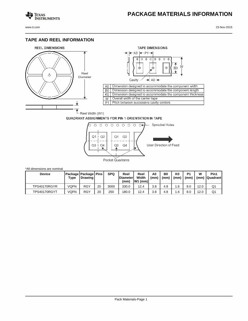
TAPE AND REEL INFORMATION
*All dimensions are nominal
Device PackageType
PackageDrawing
Pins SPQ ReelDiameter
(mm)
ReelWidth
W1 (mm)
A0(mm)
B0(mm)
K0(mm)
P1(mm)
W(mm)
Pin1Quadrant
TPS40170RGYR VQFN RGY 20 3000 330.0 12.4 3.8 4.8 1.6 8.0 12.0 Q1
TPS40170RGYT VQFN RGY 20 250 180.0 12.4 3.8 4.8 1.6 8.0 12.0 Q1
PACKAGE MATERIALS INFORMATION
www.ti.com 23-Nov-2015
Pack Materials-Page 1
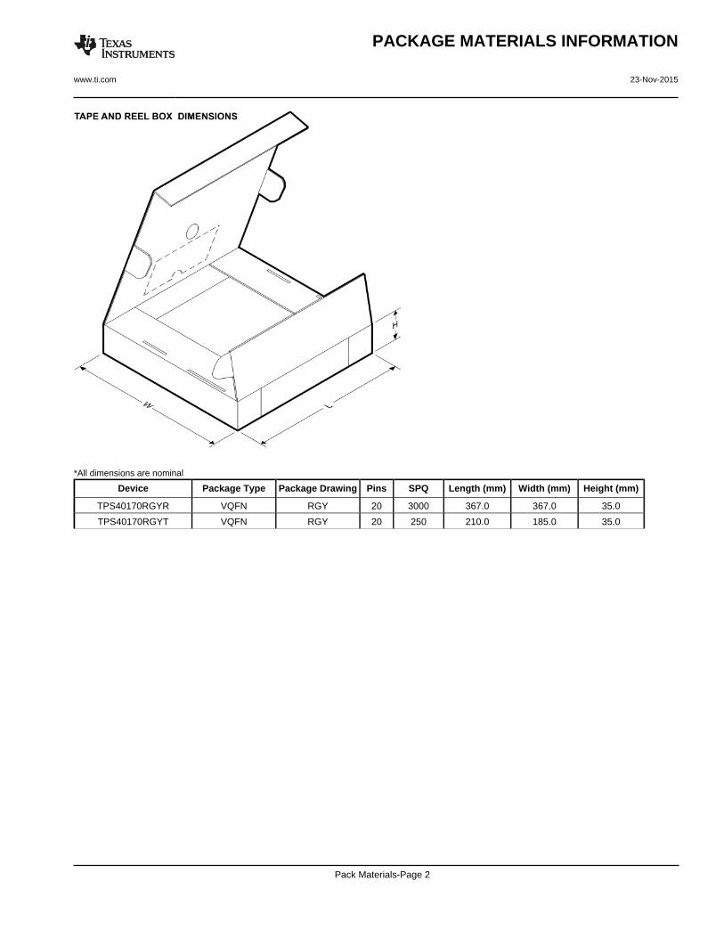
*All dimensions are nominal
Device Package Type Package Drawing Pins SPQ Length (mm) Width (mm) Height (mm)
TPS40170RGYR VQFN RGY 20 3000 367.0 367.0 35.0
TPS40170RGYT VQFN RGY 20 250 210.0 185.0 35.0
PACKAGE MATERIALS INFORMATION
www.ti.com 23-Nov-2015
Pack Materials-Page 2
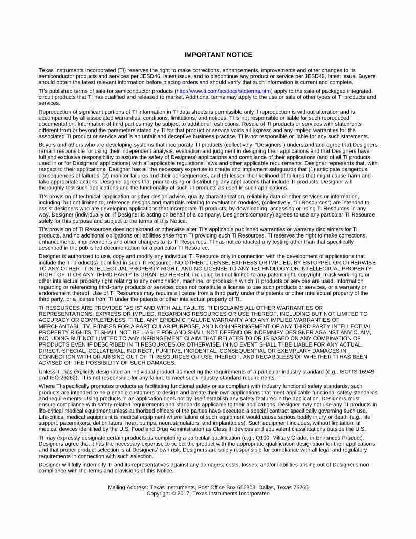
IMPORTANT NOTICE
Texas Instruments Incorporated (TI) reserves the right to make corrections, enhancements, improvements and other changes to itssemiconductor products and services per JESD46, latest issue, and to discontinue any product or service per JESD48, latest issue. Buyersshould obtain the latest relevant information before placing orders and should verify that such information is current and complete.TI’s published terms of sale for semiconductor products (http://www.ti.com/sc/docs/stdterms.htm) apply to the sale of packaged integratedcircuit products that TI has qualified and released to market. Additional terms may apply to the use or sale of other types of TI products andservices.Reproduction of significant portions of TI information in TI data sheets is permissible only if reproduction is without alteration and isaccompanied by all associated warranties, conditions, limitations, and notices. TI is not responsible or liable for such reproduceddocumentation. Information of third parties may be subject to additional restrictions. Resale of TI products or services with statementsdifferent from or beyond the parameters stated by TI for that product or service voids all express and any implied warranties for theassociated TI product or service and is an unfair and deceptive business practice. TI is not responsible or liable for any such statements.Buyers and others who are developing systems that incorporate TI products (collectively, “Designers”) understand and agree that Designersremain responsible for using their independent analysis, evaluation and judgment in designing their applications and that Designers havefull and exclusive responsibility to assure the safety of Designers' applications and compliance of their applications (and of all TI productsused in or for Designers’ applications) with all applicable regulations, laws and other applicable requirements. Designer represents that, withrespect to their applications, Designer has all the necessary expertise to create and implement safeguards that (1) anticipate dangerousconsequences of failures, (2) monitor failures and their consequences, and (3) lessen the likelihood of failures that might cause harm andtake appropriate actions. Designer agrees that prior to using or distributing any applications that include TI products, Designer willthoroughly test such applications and the functionality of such TI products as used in such applications.TI’s provision of technical, application or other design advice, quality characterization, reliability data or other services or information,including, but not limited to, reference designs and materials relating to evaluation modules, (collectively, “TI Resources”) are intended toassist designers who are developing applications that incorporate TI products; by downloading, accessing or using TI Resources in anyway, Designer (individually or, if Designer is acting on behalf of a company, Designer’s company) agrees to use any particular TI Resourcesolely for this purpose and subject to the terms of this Notice.TI’s provision of TI Resources does not expand or otherwise alter TI’s applicable published warranties or warranty disclaimers for TIproducts, and no additional obligations or liabilities arise from TI providing such TI Resources. TI reserves the right to make corrections,enhancements, improvements and other changes to its TI Resources. TI has not conducted any testing other than that specificallydescribed in the published documentation for a particular TI Resource.Designer is authorized to use, copy and modify any individual TI Resource only in connection with the development of applications thatinclude the TI product(s) identified in such TI Resource. NO OTHER LICENSE, EXPRESS OR IMPLIED, BY ESTOPPEL OR OTHERWISETO ANY OTHER TI INTELLECTUAL PROPERTY RIGHT, AND NO LICENSE TO ANY TECHNOLOGY OR INTELLECTUAL PROPERTYRIGHT OF TI OR ANY THIRD PARTY IS GRANTED HEREIN, including but not limited to any patent right, copyright, mask work right, orother intellectual property right relating to any combination, machine, or process in which TI products or services are used. Informationregarding or referencing third-party products or services does not constitute a license to use such products or services, or a warranty orendorsement thereof. Use of TI Resources may require a license from a third party under the patents or other intellectual property of thethird party, or a license from TI under the patents or other intellectual property of TI.TI RESOURCES ARE PROVIDED “AS IS” AND WITH ALL FAULTS. TI DISCLAIMS ALL OTHER WARRANTIES ORREPRESENTATIONS, EXPRESS OR IMPLIED, REGARDING RESOURCES OR USE THEREOF, INCLUDING BUT NOT LIMITED TOACCURACY OR COMPLETENESS, TITLE, ANY EPIDEMIC FAILURE WARRANTY AND ANY IMPLIED WARRANTIES OFMERCHANTABILITY, FITNESS FOR A PARTICULAR PURPOSE, AND NON-INFRINGEMENT OF ANY THIRD PARTY INTELLECTUALPROPERTY RIGHTS. TI SHALL NOT BE LIABLE FOR AND SHALL NOT DEFEND OR INDEMNIFY DESIGNER AGAINST ANY CLAIM,INCLUDING BUT NOT LIMITED TO ANY INFRINGEMENT CLAIM THAT RELATES TO OR IS BASED ON ANY COMBINATION OFPRODUCTS EVEN IF DESCRIBED IN TI RESOURCES OR OTHERWISE. IN NO EVENT SHALL TI BE LIABLE FOR ANY ACTUAL,DIRECT, SPECIAL, COLLATERAL, INDIRECT, PUNITIVE, INCIDENTAL, CONSEQUENTIAL OR EXEMPLARY DAMAGES INCONNECTION WITH OR ARISING OUT OF TI RESOURCES OR USE THEREOF, AND REGARDLESS OF WHETHER TI HAS BEENADVISED OF THE POSSIBILITY OF SUCH DAMAGES.Unless TI has explicitly designated an individual product as meeting the requirements of a particular industry standard (e.g., ISO/TS 16949and ISO 26262), TI is not responsible for any failure to meet such industry standard requirements.Where TI specifically promotes products as facilitating functional safety or as compliant with industry functional safety standards, suchproducts are intended to help enable customers to design and create their own applications that meet applicable functional safety standardsand requirements. Using products in an application does not by itself establish any safety features in the application. Designers mustensure compliance with safety-related requirements and standards applicable to their applications. Designer may not use any TI products inlife-critical medical equipment unless authorized officers of the parties have executed a special contract specifically governing such use.Life-critical medical equipment is medical equipment where failure of such equipment would cause serious bodily injury or death (e.g., lifesupport, pacemakers, defibrillators, heart pumps, neurostimulators, and implantables). Such equipment includes, without limitation, allmedical devices identified by the U.S. Food and Drug Administration as Class III devices and equivalent classifications outside the U.S.TI may expressly designate certain products as completing a particular qualification (e.g., Q100, Military Grade, or Enhanced Product).Designers agree that it has the necessary expertise to select the product with the appropriate qualification designation for their applicationsand that proper product selection is at Designers’ own risk. Designers are solely responsible for compliance with all legal and regulatoryrequirements in connection with such selection.Designer will fully indemnify TI and its representatives against any damages, costs, losses, and/or liabilities arising out of Designer’s non-compliance with the terms and provisions of this Notice.
Mailing Address: Texas Instruments, Post Office Box 655303, Dallas, Texas 75265Copyright © 2017, Texas Instruments Incorporated