Embed Size (px)
Citation preview
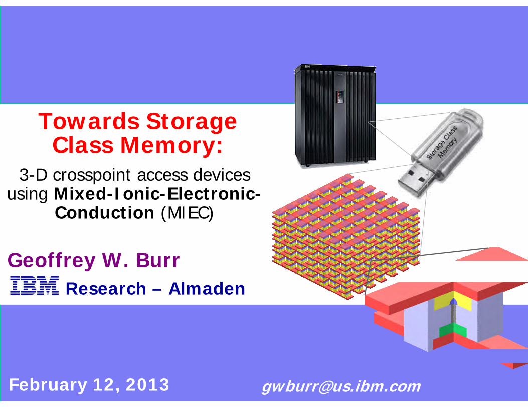
3-D crosspoint access devices using Mixed-Ionic-Electronic-
Conduction (MIEC)
Geoffrey W. Burr
February 12, 2013
Research – Almaden
Towards Storage Class Memory:
Towards SCM: 3-D crosspoint access devices using MIEC
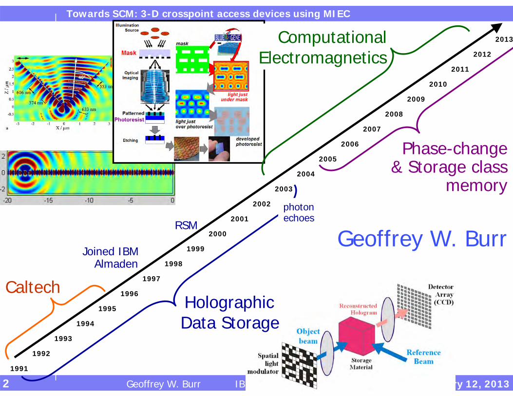
2 Geoffrey W. Burr IBM Research – Almaden February 12, 2013
2012
2013
1994
1995
1996
1997
1998
1999
2000
2001
2002
2003
2004
2005
2006
2007
2008
2009
2010
2011
1993
1991
1992
Caltech
Joined IBMAlmaden
RSM
Holographic Data Storage
ComputationalElectromagnetics
Phase-change& Storage class
memory
Geoffrey W. Burr
photonechoes

Towards SCM: 3-D crosspoint access devices using MIEC
3 Geoffrey W. Burr IBM Research – Almaden February 12, 2013
Outline Motivation
• future server-room power & space demands may require a new technology – Storage Class Memory (SCM) – combining…
the benefits of a solid-state memory (high performance and robustness) the archival capabilities and low cost of conventional HDD
3-D Crosspoint memory• High-density, high-performance Non-Volatile Memory (NVM)
STT-MRAM, RRAM, PCM
• Back-End-Of-the-Line (BEOL)-compatible access device High ON-state current for writing (>10MA/cm2) Low OFF-state leakage (<100pA >107 ON/OFF ratio) Bipolar operation (for RRAM or STT-MRAM)
Access Device based on Mixed-Ionic-Electronic-Conduction
Conclusion• With its combination of low-cost and high-performance,
SCM could impact much more than just the server-room...

Towards SCM: 3-D crosspoint access devices using MIEC
4 Geoffrey W. Burr IBM Research – Almaden February 12, 2013
Power & space in the server roomThe cache/memory/storage hierarchy is rapidly becoming the bottleneck for large systems.
We know how to create MIPS & MFLOPS cheaply and in abundance, but feeding them with data has become
the performance-limiting and most-expensive part of a system (in both $ and Watts).
• 5 million HDD 16,500 sq. ft. !! 22 Megawatts
Extrapolation to 2020(at 70% CGR need
2 GIOP/sec)
R. Freitas and W. Wilcke, Storage Class Memory: the next storage system technology –"Storage Technologies & Systems" special issue
of the IBM Journal of R&D (2008)

Towards SCM: 3-D crosspoint access devices using MIEC
5 Geoffrey W. Burr IBM Research – Almaden February 12, 2013
• 21 million HDD 70,000 sq. ft. !! 93 Megawatts
(at 90% CGR need 8.4G SIO/sec)
…yet critical applications are also undergoing a paradigm shift
Compute-centricparadigm
Typical Examples:
Bottleneck:
Main Focus: Analyze petabytes of data
Storage & I/OSearch and Mining
Analyses of social/terrorist networks
Sensor network processing
Digital media creation/transmission
Environmental & economic modeling
Data-centricparadigm
Solve differential equations
CPU / MemoryComputational Fluid Dynamics
Finite Element Analysis
Multi-body Simulations
(at 90% CGR need 1.7 PB/sec)
• 5.6 million HDD 19,000 sq. ft. !! 25 Megawatts
Extrapolationto 2020
[Freitas:2008]
Towards SCM: 3-D crosspoint access devices using MIEC
6 Geoffrey W. Burr IBM Research – Almaden February 12, 2013
ON-chipmemory
OFF-chipmemory
ON-linestorage
OFF-linestorage
Decreasingco$t
100
108
103
104
105
106
107
109
1010
Get data from DRAM/SCM (60ns)10
1 CPU operations (1ns)Get data from L2 cache (<5ns)
Read or write to DISK (5ms)
Get data from TAPE (40s)
...(in human perspective)
(T x 109)second
minute
hour
day
week
month
year
decade
century
millenium
Access time...(in ns)
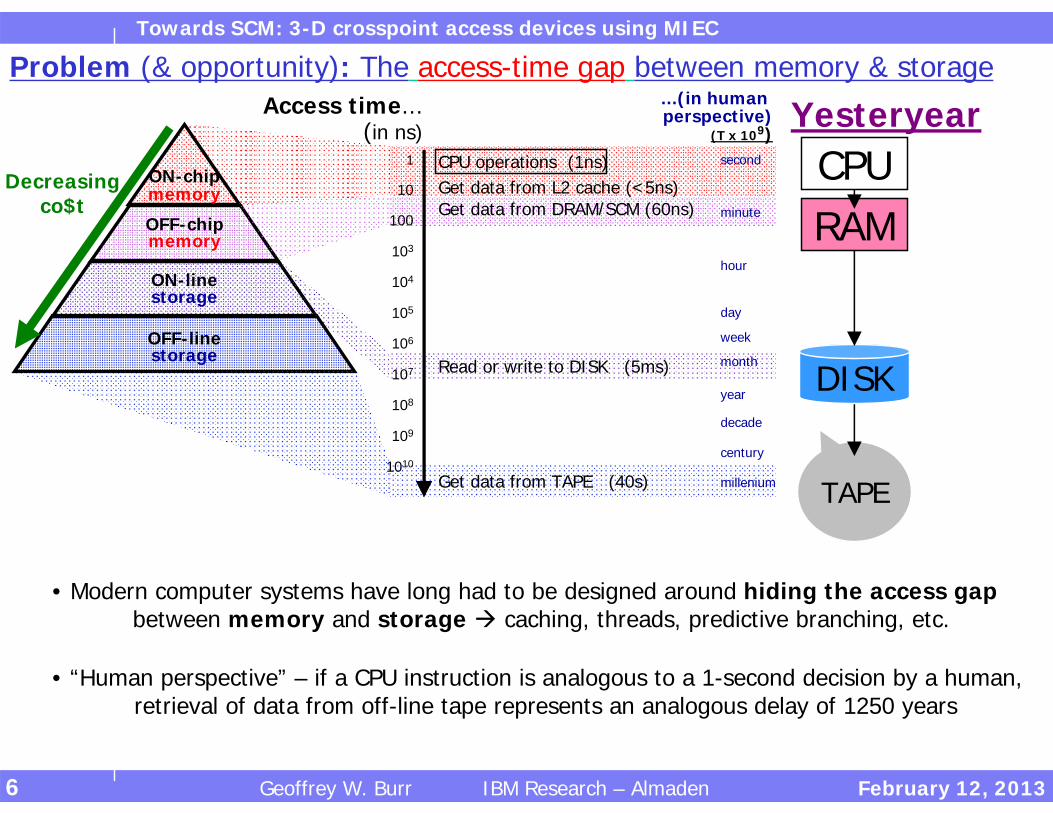
Problem (& opportunity): The access-time gap between memory & storage
TAPE
DISK
RAMCPU
Yesteryear
• Modern computer systems have long had to be designed around hiding the access gap between memory and storage caching, threads, predictive branching, etc.
• “Human perspective” – if a CPU instruction is analogous to a 1-second decision by a human,retrieval of data from off-line tape represents an analogous delay of 1250 years

Towards SCM: 3-D crosspoint access devices using MIEC
7 Geoffrey W. Burr IBM Research – Almaden February 12, 2013
Problem (& opportunity): The access-time gap between memory & storage
• Today, Solid-State Disks based on NAND Flash can offer fast ON-line storage, and storage capacities are increasing as devices scale down to smaller dimensions…
TAPE
DISK
FLASHSSD
RAMCPU
Today
TAPE
DISK
RAMCPU
…but while prices are dropping, the performance gap between memory and storageremains significant, and the already-poor device endurance of Flash is getting worse.
ON-chipmemory
OFF-chipmemory
ON-linestorage
OFF-linestorage
Decreasingco$t
100
108
103
104
105
106
107
109
1010
Get data from DRAM/SCM (60ns)10
1 CPU operations (1ns)Get data from L2 cache (<5ns)
Read or write to DISK (5ms)
Get data from TAPE (40s)
Access time...(in ns)
Write to FLASH, random (1ms)
Read a FLASH device (20 us)
Memory/storage gap
Yesteryear

Towards SCM: 3-D crosspoint access devices using MIEC
8 Geoffrey W. Burr IBM Research – Almaden February 12, 2013
Problem (& opportunity): The access-time gap between memory & storage
Research into new solid-state non-volatile memory candidates – originally motivated by finding a “successor” for NAND Flash –
has opened up several interesting ways to change the memory/storage hierarchy…
Near-future ON-chipmemory
OFF-chipmemory
ON-linestorage
OFF-linestorage
Decreasingco$t
100
108
103
104
105
106
107
109
1010
Get data from DRAM/SCM (60ns)10
1 CPU operations (1ns)Get data from L2 cache (<5ns)
Read or write to DISK (5ms)
Get data from TAPE (40s)
Access time...(in ns)
Write to FLASH, random (1ms)
Read a FLASH device (20 us)
1) Embedded Non-Volatile Memory – low-density, fast ON-chip NVM2) Embedded Storage – low density, slower ON-chip storage
3) M-type Storage Class Memory – high-density, fast OFF- (or ON*)-chip NVM4) S-type Storage Class Memory – high-density, very-near-ON-line storage
TAPE
DISK
RAMCPU
SCM
* ON-chip using 3-D packaging
Memory/storage gap

Towards SCM: 3-D crosspoint access devices using MIEC
9 Geoffrey W. Burr IBM Research – Almaden February 12, 2013
S-type vs. M-type SCM
MemoryController
DRAM
SCMI/OController
SCM
SCM
Disk
StorageController
CPUInternal
External
M-type: Synchronous• Hardware managed• Low overhead• Processor waits• New NVM not Flash• Cached or pooled memory• Persistence (data survives despite component failure or loss of power) requiresredundancy in system architecture
S-type: Asynchronous• Software managed • High overhead• Processor doesn’t wait,
(process-, thread-switching)• Flash or new NVM• Paging or storage• Persistence RAID
~1us read latency

Towards SCM: 3-D crosspoint access devices using MIEC
10 Geoffrey W. Burr IBM Research – Almaden February 12, 2013
2 4 6 8 1010ns
100ns
1ms
10ms
100ms
Rea
d La
tenc
y NAND
DRAM
(Write) Endurance
Cost/bit
Speed (Latency & Bandwidth)
Power!
Memory-typeuses
Storage-typeuses
low co$t
Cell size [F2]
Storage-type vs. memory-type Storage Class Memory
The cost basis of semiconductor processing is well understood – the paths to higher density are 1) shrinking the minimum lithographic pitch F, and 2) storing more bits PER 4F2
F F 4F2
Towards SCM: 3-D crosspoint access devices using MIEC
11 Geoffrey W. Burr IBM Research – Almaden February 12, 2013
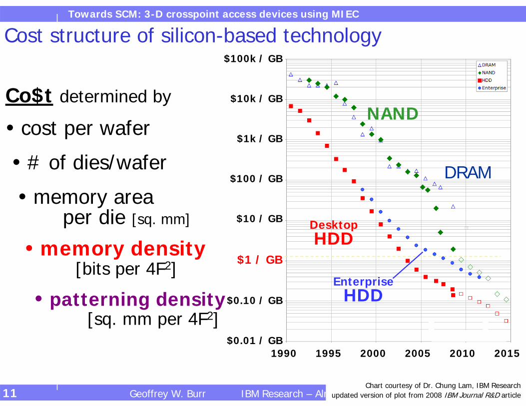
Cost structure of silicon-based technology
Co$t determined by
cost per wafer
# of dies/wafer
memory area per die [sq. mm]
memory density[bits per 4F2]
patterning density[sq. mm per 4F2]
Chart courtesy of Dr. Chung Lam, IBM Researchupdated version of plot from 2008 IBM Journal R&D article
$1 / GB
$10 / GB
$100 / GB
$1k / GB
$10k / GB
$100k / GB
$0.10 / GB
$0.01 / GB
NAND
DesktopHDD
DRAM
1990 1995 2000 2005 2010 2015
EnterpriseHDD

Towards SCM: 3-D crosspoint access devices using MIEC
12 Geoffrey W. Burr IBM Research – Almaden February 12, 2013
Storage Class Memory need 3-D crosspoint arrays
Performance
Cost
NOR FLASH
NAND FLASH
DRAM
SRAM
HDD
STORAGECLASS
MEMORY

Towards SCM: 3-D crosspoint access devices using MIEC
13 Geoffrey W. Burr IBM Research – Almaden February 12, 2013
Outline Motivation
• future server-room power & space demands may require a new technology – Storage Class Memory (SCM) – combining…
the benefits of a solid-state memory (high performance and robustness) the archival capabilities and low cost of conventional HDD
3-D Crosspoint memory• High-density, high-performance Non-Volatile Memory (NVM)
STT-MRAM, RRAM, PCM
• Back-End-Of-the-Line (BEOL)-compatible access device High ON-state current for writing (>10MA/cm2) Low OFF-state leakage (<100pA >107 ON/OFF ratio) Bipolar operation (for RRAM or STT-MRAM)
Access Device based on Mixed-Ionic-Electronic-Conduction
Conclusion• With its combination of low-cost and high-performance,
SCM could impact much more than just the server-room...

Towards SCM: 3-D crosspoint access devices using MIEC
14 Geoffrey W. Burr IBM Research – Almaden February 12, 2013
Storage Class Memory at IBM Almaden2004
2005
2006
2007
2008
2009
2010
2011
2012
IEDM2006
IEDM 2007
VLSI 2007
IEDM 2010
IBM/Macronix/QimondaJoint Project begins
Science 2009JAP 2012
(MRS 2013)

Towards SCM: 3-D crosspoint access devices using MIEC
15 Geoffrey W. Burr IBM Research – Almaden February 12, 2013
2004
2005
2006
2007
2008
2009
2012
IEDM2006
IEDM 2007
VLSI 2007
IEDM 2010
IBM/Macronix/QimondaJoint Project begins
2010
2011
VLSI 2010
VLSI 2011
IEDM2012
Storage Class Memory at IBM Almaden
VLSI 2012

Towards SCM: 3-D crosspoint access devices using MIEC
16 Geoffrey W. Burr IBM Research – Almaden February 12, 2013
Ingredients of crosspoint memory
NVM memory element
plus access device
Generic SCM Array
• Improved FLASH
• Magnetic Spin Torque Transfer STT-RAM Magnetic Racetrack
• Phase Change RAM
• Resistive RAM
2) High-density access device (A.D.)
1) NVM element
• 2-D – silicon transistor or diode
• 3-D higher density per 4F2
• polysilicon diode (but <400oC processing?)
• MIEC A.D. (Mixed Ionic-Electronic Conduction)
• OTS A.D. (Ovonic Threshold Switch)• Conductive oxide tunnel barrier A.D.

Towards SCM: 3-D crosspoint access devices using MIEC
17 Geoffrey W. Burr IBM Research – Almaden February 12, 2013
Limitations of FlashAsymmetric performance
Writes much slower than reads
Program/erase cycleBlock-based, no write-in-place
Data retention and Non-volatilityRetention gets worse as Flash scales down
17
60
200
7
40100
1
10
100
1000
USB disk LapTop Enterprise
MB
/s
Sustained Read Bandwidth Sustained Write Bandwidth
200010000
52000
49
17000
3000
10
100
1000
10000
100000
USB disk LapTop Enterprise
IOPS
Maximum Random Read IOPs Maximum Random Write IOPs
Endurance
• Single level cell (SLC) 105 writes/cell
• Multi level cell (MLC) 104 writes/cell
• Triple level cell (TLC) ~300 writes/cell
Future outlook
• Scaling focussed solely on density
• 3-D schemes exist but are complex

Towards SCM: 3-D crosspoint access devices using MIEC
18 Geoffrey W. Burr IBM Research – Almaden February 12, 2013
STT (Spin-Torque-Transfer) RAM• Controlled switching of free magnetic layer in a magnetic tunnel junction using current, leading to two distinct resistance states
• Inherently very fast almost as fast as DRAM• Much better endurance than Flash or PCM• Radiation-tolerant• Materials are Back-End-Of-the-Line compatible• Simple cell structure reduced processing costs
Strengths
Weaknesses• Achieving low switching current/power is not easy• BEOL temperatures can affect STT-MRAM device stack• Resistance contrast is quite low (2-3x) achieving tight distributions is ultra-critical• High-temperature retention strongly affected by scaling below F~50nm• Tradeoff between fastest switching and switching reliability
Bit Line
Plate Line
Word Line
Outlook: Strong outlook for an Embedded Non-Volatile Memory to replace/augment DRAM.
While near-term prospects for high-density SCM with STT-RAM may seem dim, Racetrack Memory offers hope for using STT concepts to create vertical “shift-register” of domain walls potential densities of 10-100 bits/F2

Towards SCM: 3-D crosspoint access devices using MIEC
19 Geoffrey W. Burr IBM Research – Almaden February 12, 2013
• Very mature (large-scale demos & products)• Industry consensus on material GeSbTe or GST• Large resistance contrast analog states for MLC • Offers much better endurance than Flash• Shown to be highly scalable (still works at ultra-small F) and Back-End-Of-the-Line compatible• Can be very fast (depending on material & doping)
Phase-change RAM Phase Change Material
‘heater’wire
insulator
word line
bit lineaccess device
• Switching between low-resistance crystalline, and high-resistance amorphous phases, controlled through power & duration of electrical pulses
Strengths
Weaknesses• RESET step to high resistance requires melting power-hungry, thermal crosstalk?
To keep switching power down sub-lithographic feature and high-current Access DeviceTo fill small feature ALD or CVD difficult now to replace GST with a better material
Variability in small features broadens resistance distributions• 10-year retention at elevated temperatures can be an issue recrystallization• Device characteristics change over time due to elemental segregation device failure• MLC strongly affected by relaxation of amorphous phase “resistance drift”
Outlook: NOR-replacement products now shipping if yield-learning successful and MLC drift-mitigation and/or 3-D Access Devices can offer high-density (=low-cost), then opportunity for NAND replacement, S-type, and then finally M-type SCM may follow

Towards SCM: 3-D crosspoint access devices using MIEC
20 Geoffrey W. Burr IBM Research – Almaden February 12, 2013
RESET
Resistive RAM Voltage-controlled formation & dissipation of an oxygen-vacancy (or metallic) filament through an otherwise insulating layer
• Good retention at elevated-temperatures• Simple cell structure reduced processing costs• Both fast and ultra-low-current switching have been demonstrated• Some RRAM materials are Back-End-Of-the-Line compatible• Relatively new field high hopes for improved material concepts• Less “gating” Intellectual Property to license• Some RRAM concepts offer co-integrated NVM & Access Device • Numerous ongoing development efforts
Strengths
Weaknesses• Highly immature technology – wide variation in materials hampers cross-industry learning• Demonstrated endurance is slightly better than Flash, but lower than PCM or STT-RAM• Switching reliability an issue, even within single devices, and read disturb can be an issue• An initial high-voltage “forming” step is often required• To attain low RESET switching currents, circuit must constrain current during previous SET• Unipolar and bipolar versions – bipolar typically better in both write margins & endurance,
but then requires an unconventional bipolar-capable Access Device (transistor or diode is out)• High array yield with minimal “outlier” devices not yet demonstrated• Tradeoff between switching speed, long-term retention, and reliability not yet explored
Outlook: Outlook is unclear. Emergence of a strong material candidate offering high array yield & reliability could focus industry efforts considerably. Absent that, many uncertainties remain about prospects for reliable storage & memory products.
Top electrode
Bottom electrode“Forming”
step
SET
oxide
Conductivefilament

Towards SCM: 3-D crosspoint access devices using MIEC
21 Geoffrey W. Burr IBM Research – Almaden February 12, 2013
NVM memory element
plus access device
Generic SCM Array
• Improved FLASH
• Magnetic Spin Torque Transfer STT-RAM Magnetic Racetrack
• Phase Change RAM
• Resistive RAM
2) High-density access device (A.D.)
1) NVM element
• 2-D – silicon transistor or diode
• 3-D higher density per 4F2
• polysilicon diode (but <400oC processing?)
• MIEC A.D. (Mixed Ionic-Electronic Conduction)
• OTS A.D. (Ovonic Threshold Switch)• Conductive oxide tunnel barrier A.D.
Ingredients of crosspoint memory

Towards SCM: 3-D crosspoint access devices using MIEC
22 Geoffrey W. Burr IBM Research – Almaden February 12, 2013
High density 3D Multilayer Crosspoint Memory Array
Effective cell size: 4F2 Effective cell size: 4F2/L
Stack ‘L’ layers in 3D
F = minimum litho. feature size
As a result of the cost-basis of semiconductor manufacturing, memory cost is inversely related to bit density
Since they effectively store more bits per 4F2 footprint,
3D crosspoint arrays a route to low cost memory
(adapted from Burr, EIPBN 2008)

Towards SCM: 3-D crosspoint access devices using MIEC
23 Geoffrey W. Burr IBM Research – Almaden February 12, 2013
Large arrays require an Access Device at each element
Memory Element (PCM, RRAM etc.)
Access Device (Selector)
Apply V
Current ‘sneak path’problem
Access device needed in series with memory element
• Cut off current ‘sneak paths’ that lead to incorrect sensing and wasted power
• Typically diodes used as access devices• Could also use devices with highly non-linear I-V curves
Sense I

Towards SCM: 3-D crosspoint access devices using MIEC
24 Geoffrey W. Burr IBM Research – Almaden February 12, 2013
Requirements for an Access Device for 3D Crosspoint Memory
PCM or RRAM
Access Device
• High ON-state current density>10 MA/cm2 for PCM / RRAM RESET
• Low OFF-state leakage current>107 ON/OFF ratio, andwide low-leakage (< 100pA) voltage zone to accommodate half-selected cells in large arrays
• Back-End process compatible<400C processing to allow 3D stacking
• Bipolar operationneeded for optimum RRAM operation
IBM’s MIEC-based access device satisfies all these criteria

Towards SCM: 3-D crosspoint access devices using MIEC
25 Geoffrey W. Burr IBM Research – Almaden February 12, 2013
100A
1A
100nA
10nA
1nA
100pA
10pA
0.30.1-0.1-0.3-0.5
|Cur
rent
|
AppliedVoltage
[V]1pA
10A
0.5
W
gapoverlap
W
gapoverlap
W=200nmGap=100nmOverlap=250nm
200nminert TEC
80nm BEC
10A
1A
100nA
10nA
1nA
100pA
10pA
1pA
100A
|Cur
rent
|
-1 -0.8 -0.6 -0.4 -0.2 0 0.2 0.4 0.6 0.8
Voltage [V]
MIEC
TEC
ILDBEC
poly-Si series resistor
MIEC
TEC
ILDBEC
poly-Si series resistor
Lateral (bridge) deviceVertical device (scaled TEC)
• Devices fabricated on 4inch wafers• Voltage margin @ 10nA of 0.85V• Suitable (desirable) for bipolar memory elements such as RRAM
MIEC access devices can operate in both polarities(Gopalakrishnan et al, 2010 VLSI Tech. Sym.)
MIEC access devices offer highly nonlinear & Bipolar I-V Curves
Towards SCM: 3-D crosspoint access devices using MIEC
26 Geoffrey W. Burr IBM Research – Almaden February 12, 2013
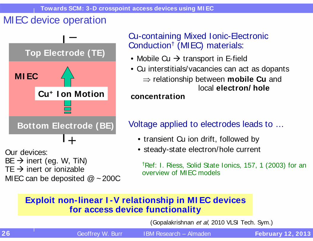
Bottom Electrode (BE)
Top Electrode (TE)
MIEC
Cu+ Ion Motion
Cu-containing Mixed Ionic-Electronic Conduction† (MIEC) materials:• Mobile Cu transport in E-field• Cu interstitials/vacancies can act as dopants
relationship between mobile Cu and local electron/hole
concentration
Voltage applied to electrodes leads to …
• transient Cu ion drift, followed by• steady-state electron/hole currentOur devices:
BE inert (eg. W, TiN)TE inert or ionizableMIEC can be deposited @ ~200C
Exploit non-linear I-V relationship in MIEC devices for access device functionality
(Gopalakrishnan et al, 2010 VLSI Tech. Sym.)
†Ref: I. Riess, Solid State Ionics, 157, 1 (2003) for an overview of MIEC models
MIEC device operation

Towards SCM: 3-D crosspoint access devices using MIEC
27 Geoffrey W. Burr IBM Research – Almaden February 12, 2013
MIEC devices – 200mm wafer integration demonstrated
As-deposited
Post-CMP
TEM x-section
180 nm CMOS Front-End 1T-1MIEC
(1 transistor + 1 MIEC access device)
CMP process for MIEC material with modified commercial Cu slurry
self-aligned MIEC Diode-in-Via (DIV) in a 200 mm wafer process(Shenoy et al, 2011 VLSI Tech. Sym.)

Towards SCM: 3-D crosspoint access devices using MIEC
28 Geoffrey W. Burr IBM Research – Almaden February 12, 2013
MIEC devices support ultra-low leakage currents (needed for successful half- and un-select within large arrays)
Voltage margin @ 10nA of 1.1V~10 pA leakage currents near 0V & wide range with <100pA
(Burr et al, 2012 VLSI Tech. Sym.)

Towards SCM: 3-D crosspoint access devices using MIEC
29 Geoffrey W. Burr IBM Research – Almaden February 12, 2013
Scope
Pulsegenerator
V
t
Current
t50W
100’s of uA pulse currents ON/OFF ratio >107
(Shenoy et al, 2011 VLSI Tech. Sym.)
MIEC devices can supply LARGE driving currents (needed for successful write of power-hungry NVM candidates)

Towards SCM: 3-D crosspoint access devices using MIEC
30 Geoffrey W. Burr IBM Research – Almaden February 12, 2013
Requirements for an Access Device for 3D Crosspoint Memory
PCM or RRAM
Access Device
High ON-state current density>10 MA/cm2 for PCM / RRAM RESET
Low OFF-state leakage current>107 ON/OFF ratio, andwide low-leakage (< 100pA) voltage zone to accommodate half-selected cells in large arrays
Back-End process compatible<400C processing to allow 3D stacking
Bipolar operationneeded for optimum RRAM operation
• variability?• yield?• co-integration with NVM?• turn-ON speed for write?• endurance?• manufacturability?• scalability?
• long-term leakage?• turn-OFF speed?• turn-ON speed for read?

Towards SCM: 3-D crosspoint access devices using MIEC
31 Geoffrey W. Burr IBM Research – Almaden February 12, 2013
5x10 arrays of FET-connected DIVs
• Voltage margin (Vm) ~1.1V • Low inter-device variability
Integrated small arrays of MIEC DIVs with high yield
(Shenoy et al, 2011 VLSI Tech. Sym.)
Multiple MIEC devices can be made with similar characteristics(essential for reading, especially if SNR from the NVM is low)

Towards SCM: 3-D crosspoint access devices using MIEC
32 Geoffrey W. Burr IBM Research – Almaden February 12, 2013
Large Arrays of MIEC have been integrated at 100% yield
100% yield and tight distributions in 512 kbit 1T-1MIEC array(Burr et al, 2012 VLSI Tech. Sym.)

Towards SCM: 3-D crosspoint access devices using MIEC
33 Geoffrey W. Burr IBM Research – Almaden February 12, 2013
Demonstrated > 105 cycles of PCM SET/RESET through stacked MIEC access device
(Burr et al, 2012 VLSI Tech. Sym.)
MIEC has been integrated together with PCM in 200mm process

Towards SCM: 3-D crosspoint access devices using MIEC
34 Geoffrey W. Burr IBM Research – Almaden February 12, 2013
MIEC access device can supply >150uA in 15ns …sufficient to RESET PCM
(Virwani et al, IEDM 2012)
0
100
200
300
400
500
Time
Current[uA]
5 ns/division15ns
a)Increasing pulseamplitude
RESET current [uA]100 150 200 300 400
30nA
100nA
300nA
1uA
Rea
d C
urre
nt@
660m
V
post-SET
RESETPost-
MIEC supports 15ns writes of PCM suitable for M-class SCM

Towards SCM: 3-D crosspoint access devices using MIEC
35 Geoffrey W. Burr IBM Research – Almaden February 12, 2013
OFF current at -0.2V100pA
1nA
10nA
100nA
1A
10A
100A
|Cur
rent
|
ON current >5Asufficient for PCM-read
(Rs~30k Vapplied~ -0.8V)
OFF current at -0.3V
Pulse duration ~2s
100 1000 104 105 106 108 109 1010107
Pulses
80 nm BEC Wide-area ionizable TEC
Testing time-limited!
Low current (memory READ) endurance > 1010 cycles
(Gopalakrishnan et al, 2010 VLSI Tech. Sym.)
MIEC endurance at low current >> 1e10 cycles

Towards SCM: 3-D crosspoint access devices using MIEC
36 Geoffrey W. Burr IBM Research – Almaden February 12, 2013
MIEC endurance at high current is finite leakage increases
DC I-V curves monitored in between 100uA pulses
Leakage current rises …
… and voltage margin shrinks
After many cycles …
High current (memory WRITE) endurance is finite.
(Shenoy et al, 2011 VLSI Tech. Sym.)

Towards SCM: 3-D crosspoint access devices using MIEC
37 Geoffrey W. Burr IBM Research – Almaden February 12, 2013
Endurance depends inversely on current (exponential) and pulse duration
(Shenoy et al, 2011 VLSI Tech. Sym.)
MIEC endurance scales sharply with current (NOT current density)

Towards SCM: 3-D crosspoint access devices using MIEC
38 Geoffrey W. Burr IBM Research – Almaden February 12, 2013
Strong current-dependence of MIEC access device endurance persists across many different device structures
Expect even higher MIEC endurance for RRAM (IPROG/ERASE <100uA)
(Shenoy et al, 2011 VLSI Tech. Sym.)
>108 endurance for sub-45nm-node PCM!( IRESET < 150 A )
MIEC endurance at modest write currents > 1e8
Towards SCM: 3-D crosspoint access devices using MIEC
39 Geoffrey W. Burr IBM Research – Almaden February 12, 2013
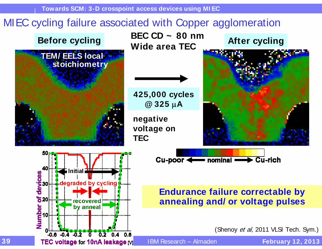
Before cycling After cycling
425,000 cycles @ 325 A
TEM/EELS local stoichiometry
BEC CD ~ 80 nmWide area TEC
negative voltage on TEC
(Shenoy et al, 2011 VLSI Tech. Sym.)
MIEC cycling failure associated with Copper agglomeration
Endurance failure correctable by annealing and/or voltage pulses

Towards SCM: 3-D crosspoint access devices using MIEC
40 Geoffrey W. Burr IBM Research – Almaden February 12, 2013
Requirements for an Access Device for 3D Crosspoint Memory
PCM or RRAM
Access Device
High ON-state current density>10 MA/cm2 for PCM / RRAM RESET
Low OFF-state leakage current>107 ON/OFF ratio, andwide low-leakage (< 100pA) voltage zone to accommodate half-selected cells in large arrays
Back-End process compatible<400C processing to allow 3D stacking
Bipolar operationneeded for optimum RRAM operation
variability? yield? co-integration with NVM? turn-ON speed for write? endurance?• manufacturability?• scalability?
• long-term leakage?• turn-OFF speed?• turn-ON speed for read?

Towards SCM: 3-D crosspoint access devices using MIEC
41 Geoffrey W. Burr IBM Research – Almaden February 12, 2013
Large thermal process budget window Manufacturable deposition
Process optimization for higher Vm
Rapid learning cycles enabled by cAFM
(Burr et al, 2012 VLSI Tech. Sym.)
Short loop process flows on relevant structures
Conductive AFM rapid exploration of processes & materials

Towards SCM: 3-D crosspoint access devices using MIEC
42 Geoffrey W. Burr IBM Research – Almaden February 12, 2013
80nm40nm
1m10A
1A
100nA
10nA
1nA
100pA
|Cur
rent
|
10pA
Vbias-0.50V
-0.35V
-0.30V
-0.25V
Via height:20nm
200 400 600 800
Time [ns]0
0
0.4
0.8
1.2
1.6
Volta
ge [V
]
1000 104 105 106Via height: 40nm
250nm
Via area = CD2 [nm2]
Wide-area Ionizable TEC
19 nm
Current scales well with BEC size over several orders of magnitude
Suggests non-filamentary nature of operation mechanism(Gopalakrishnan et al, 2010 VLSI Tech. Sym.)
Lateral scaling of just BEC size

Towards SCM: 3-D crosspoint access devices using MIEC
43 Geoffrey W. Burr IBM Research – Almaden February 12, 2013
Selector functionality is maintained in fully confined MIEC devices with reduced TEC and BEC size
Voltage margin increased with smaller TEC CD
(Virwani et al, 2012 IEDM)
(Shenoy et al, 2011 VLSI Tech. Sym.)
Consistent with trend seen on earlier devices
Lateral scaling of TEC size (slide 1 of 3)
139nm
89nm
48nm
139nm
Correction to 2012 IEDM

Towards SCM: 3-D crosspoint access devices using MIEC
44 Geoffrey W. Burr IBM Research – Almaden February 12, 2013
Ultra-scaled MIEC access devices can still deliver >100uA pulse currents in both polarities
(Virwani et al, 2012 IEDM)
Lateral scaling of TEC size (slide 2 of 3)

Towards SCM: 3-D crosspoint access devices using MIEC
45 Geoffrey W. Burr IBM Research – Almaden February 12, 2013
No lower limit to lateral scaling has been found so far
(Virwani et al, 2012 IEDM)
Sub-30nm lateral CD MIEC device
Lateral scaling of TEC size (slide 3 of 3)

Towards SCM: 3-D crosspoint access devices using MIEC
46 Geoffrey W. Burr IBM Research – Almaden February 12, 2013
SiN
Si wafer
BECoxide
C-AFMtip
TEC
MIEC dmin
Cumulative distribution plots of 10nA MIEC voltage margin
MIEC devices are well behaved down to 12nm minimum inter-electrode distance (dmin)
(Virwani et al, 2012 IEDM)
Thickness scaling trends

Towards SCM: 3-D crosspoint access devices using MIEC
47 Geoffrey W. Burr IBM Research – Almaden February 12, 2013
Start to see some failures in arrays of MIEC devices with dmin ~12nm Leakage current increases
(Virwani et al, 2012 IEDM)
Thickness scaling trends – failure analysis (slide 1 of 2)

Towards SCM: 3-D crosspoint access devices using MIEC
48 Geoffrey W. Burr IBM Research – Almaden February 12, 2013
Lower limit seen for thickness scaling of this MIEC access device
(Virwani et al, 2012 IEDM)Good
Good
Bad
Use TEM to correlate device failures to MIEC thickness
Thickness scaling trends – failure analysis (slide 2 of 2)

Towards SCM: 3-D crosspoint access devices using MIEC
49 Geoffrey W. Burr IBM Research – Almaden February 12, 2013
Requirements for an Access Device for 3D Crosspoint Memory
PCM or RRAM
Access Device
High ON-state current density>10 MA/cm2 for PCM / RRAM RESET
Low OFF-state leakage current>107 ON/OFF ratio, andwide low-leakage (< 100pA) voltage zone to accommodate half-selected cells in large arrays
Back-End process compatible<400C processing to allow 3D stacking
Bipolar operationneeded for optimum RRAM operation
variability? yield? co-integration with NVM? turn-ON speed for write? endurance? manufacturability? scalability?
• long-term leakage?• turn-OFF speed?• turn-ON speed for read?

Towards SCM: 3-D crosspoint access devices using MIEC
50 Geoffrey W. Burr IBM Research – Almaden February 12, 2013
Novel Mixed-Ionic-Electronic-Conduction (MIEC) Access DeviceStrengths
•High enough ON currents for PCM –cycling of PCM has been demonstrated•Low enough OFF current for large arrays•Very large (>>1e10) endurance for typical 5uA read currents•Voltage margins > 1.5V with tight distributions sufficient for large arrays•CMP process demonstrated•512kBit arrays demonstrated w/ 100% yield•Scalable to <30nm CD, <12nm thickness•Capable of 15ns write, <<1us read
Weaknesses•Maximum voltage across companion NVM during switching must be low (1-2V) influences half-select condition and thus achievable array size•Endurance during NVM programming is strongly dependent on programming current
Gopalakrishnan, VLSI 2010Shenoy, VLSI 2011
Burr, VLSI 2012Virwani, IEDM 2012

Towards SCM: 3-D crosspoint access devices using MIEC
51 Geoffrey W. Burr IBM Research – Almaden February 12, 2013
Competitive Outlook among emerging NVMs
High Speed
Low co$t
Embedded Non-Volatile Memory(low-density, fast ON-chip NVM)
• STT-RAM? CBRAM?
Embedded Storage(low density, slower ON-chip storage)
• NAND? (but complicated process)
• RRAM?/PCM?
Future NOR applications(program code, etc.)
• PCM (but market disappearing)
Future NAND applications(consumer devices, etc.)
• 3-D NAND (but crossover to succeed 20nm conventional NAND may require >50 layers!)
• PCM?/RRAM?
M-type Storage Class Memory(high-density, fast OFF- (or ON*)-chip NVM)
• CBRAM? STT-RAM?• PCM?/RRAM?• Racetrack? (future?)
S-type Storage Class Memory(high-density, very-near-ON-line storage)
1) PCM?/RRAM?2) Racetrack? (future?)
* ON-chip using 3-D packaging

Towards SCM: 3-D crosspoint access devices using MIEC
52 Geoffrey W. Burr IBM Research – Almaden February 12, 2013
DeviceAvailabilityPaths towards SCM
Embedded Storage(low density,
slower ON-chip storage)
S-type SCM(high-density,
near-ON-line storage)
1-10usemerging NVM RRAM? PCM? CBRAM?
* ON-chip using 3-D packaging
M-type SCM(high-density,
fast OFF-(or ON*)-chip NVM)
EmbeddedNon-Volatile Memory(low-density, fast ON-chip NVM)
<<1usemerging NVM STT-RAM? CBRAM?PCM??/RRAM??
Future DRAM (working memory, etc.)
DRAM
Capitalinvestment Applications
3-D NANDNAND Future NAND applications(consumer devices, etc.)
Co$t
unlikely, butpossible path

Towards SCM: 3-D crosspoint access devices using MIEC
53 Geoffrey W. Burr IBM Research – Almaden February 12, 2013
What does the future hold?
• Consumer disk and enterprise tape will persist for the foreseeable future
• Flash will come into its own (in enterprise systems)
• Flash may drive out enterprise disk, and if it doesn’t, SCM will
• When will SCM arrive? That will depend on the path the NAND industry takes after the 16-20nm node…
• 3-D NAND succeeds new NVMs (such as PCM, RRAM, STT-RAM) will developslowly, driven only by SCM/embedded market
• 3-D NAND fails or is late one new NVM will be driven rapidly by NAND market
• If the latter, SCM could become the dominant storage technology by 2020
• The application software stack will be redesigned to utilize SCM-enabled persistent memory

Towards SCM: 3-D crosspoint access devices using MIEC
54 Geoffrey W. Burr IBM Research – Almaden February 12, 2013
For more information & acknowledgements• K. Virwani, G. W. Burr, Rohit S. Shenoy, C. T. Rettner, A. Padilla, T. Topuria, P. M. Rice, G. Ho, R. S. King, K. Nguyen, A. N. Bowers, M. Jurich, M. BrightSky, E. A. Joseph, A. J. Kellock, N. Arellano, B. N. Kurdi and Kailash Gopalakrishnan, “Sub-30nm scaling and high-speed operation of fully-confined Access-Devices for 3-D crosspoint memory based on Mixed-Ionic-Electronic-Conduction (MIEC) Materials,” IEDM Technical Digest, 2.7, (2012).
• Geoffrey W. Burr, Kumar Virwani, R. S. Shenoy, Alvaro Padilla, M. BrightSky, E. A. Joseph, M. Lofaro, A. J. Kellock, R. S. King, K. Nguyen, A. N. Bowers, M. Jurich, C. T. Rettner, B. Jackson, D. S. Bethune, R. M. Shelby, T. Topuria, N. Arellano, P. M. Rice, Bulent N. Kurdi, and K. Gopalakrishnan, “Large-scale (512kbit) integration of Multilayer-ready Access-Devices based on Mixed-Ionic-Electronic-Conduction (MIEC) at 100% yield,” Symposium on VLSI Technology, T5.4, (2012).
• R. S. Shenoy, K. Gopalakrishnan, Bryan Jackson, K. Virwani, G. W. Burr, C. T. Rettner, A. Padilla, Don S. Bethune, R. M. Shelby, A. J. Kellock, M. Breitwisch, E. A. Joseph, R. Dasaka, R. S. King, K. Nguyen, A. N. Bowers, M. Jurich, A. M. Friz, T. Topuria, P. M. Rice, and B. N. Kurdi, “Endurance and Scaling Trends of Novel Access-Devices for Multi-Layer Crosspoint Memory based on Mixed Ionic Electronic Conduction (MIEC) Materials,” Symposium on VLSI Technology, T5B-1, (2011).
• K. Gopalakrishnan, R. S. Shenoy, C. T. Rettner, K. Virwani, Don S. Bethune, R. M. Shelby, G. W. Burr, A. J. Kellock, R. S. King, K. Nguyen, A. N. Bowers, M. Jurich, B. Jackson, A. M. Friz, T. Topuria, P. M. Rice, and B. N. Kurdi, "Highly-Scalable Novel Access Device based on Mixed Ionic Electronic Conduction (MIEC) Materials for High Density Phase Change Memory (PCM) Arrays," Symposium on VLSI Technology, 19.4, (2010).
• G. W. Burr, Matt J. Breitwisch, Michele Franceschini, Davide Garetto, K. Gopalakrishnan, B. Jackson, B. Kurdi, C. Lam, Luis A. Lastras, A. Padilla, Bipin Rajendran, S. Raoux, and R. Shenoy, "Phase change memory technology," Journal of Vacuum Science & Technology B, 28(2), 223-262, (2010).
• G. W. Burr, B. N. Kurdi, J. C. Scott, C. H. Lam, K. Gopalakrishnan, and R. S. Shenoy, "An overview of candidate device technologies for Storage-Class Memory," IBM Journal of Research and Development, 52(4/5), 449 (2008).
• S. Raoux, G. W. Burr, M. J. Breitwisch, C. T. Rettner, Y. Chen, R. M. Shelby, M. Salinga, D. Krebs, S. Chen, H. L. Lung, and C. H. Lam, "Phase-change random access memory — a scalable technology," IBM Journal of Research and Development, 52(4/5), 465,, (2008).
• Rich Freitas and Winfried Wilcke, “Storage Class Memory, the next storage system technology,” IBM Journal of Research and Development, 52(4/5), 439, (2008).
• Yi-Chou Chen, Charlie T. Rettner, Simone Raoux, G. W. Burr, S. H. Chen, R. M. (Bob) Shelby, M. Salinga, W. P. Risk, T. D. Happ, G. M. McClelland, M. Breitwisch, A. Schrott, J. B. Philipp, M. H. Lee, R. Cheek, T. Nirschl, M. Lamorey, C. F. Chen, E. Joseph, S. Zaidi, B. Yee, H. L. Lung, R. Bergmann, and Chung Lam, "Ultra-Thin Phase-Change Bridge Memory Device Using GeSb," IEDM Technical Digest, paper S30P3, (2006).
http://researcher.ibm.com, search for “Burr” or “Storage Class Memory”


![Organic Memory Devices Using C60 and Insulating Polymer Memory...molecular memories have shown promise towards technological feasibility [2]. In contrast, there have been relatively](https://img.pdfslide.us/doc/110x75/5ecb11b7d7384c0f65747665/organic-memory-devices-using-c60-and-insulating-memory-molecular-memories-have.jpg)